Embed Size (px)
DESCRIPTION
Ralink RT3050 RT3052
Citation preview

RT3050/52 Datasheet
Preliminary Revision August 14, 2008
DSR3050/52_V.2.0_081408 -1- Form No.:QS-073-F02 Rev.:1 Kept by: DCC Ret. T ime: 5 Years
Application
802.11 b/g/n AP/Router • NAS
Dual Band Concurrent Router • iNIC
The RT3052 SOC combines Ralink’s 802.11n draft
compliant 2T2R MAC/BBP/RF, a high performance
384MHz MIPS24KEc CPU core, 5-port integrated
10/100 Ethernet switch/PHY, an USB OTG and a
Gigabit Ethernet MAC. With the RT3052, there are
very few external components required for 2.4GHz
11n wireless products. The RT3052 employs Ralink
2nd generation 11n technologies for longer range and
better throughput. The embedded high performance
CPU can process advanced applications effortlessly,
such as routing, security and VOIP. The USB port can
be configured to access external storage for Digital
Home applications. In addition, the RT3052 has rich
hardware interfaces (SPI/I2S/I2C/UART/GMAC) to
enable many possible applications.
Features Embedded 2T2R 2.4G CMOS RF Embedded 802.11n 2T2R MAC/BBP w/MLD
enhancement 300Mbps PHY data rate 1x1/1x2/2x2 modes
20Mhz/40Mhz channel width Legacy and high throughout modes Reverse Data Grant (RDG) support Compressed Block ACK
Up to 256 clients Multiple BSSID (up to 8) WEP64/128, WPA, WPA2 engines QOS - WMM, WMM Power Save
Hardware frame aggregation
International Regulation - 802.11h TPC MIPS 24KEc 384Mhz with 32KB I cache/16KB D
cache
Support 16/32-bit SDR SDRAM (up-to 64M bytes) SDRAM data [31:16] sre pins shared with GPIO Support boot from 8/16-bit parallel NOR type Flash
(up-to 16M bytes))
Support boot from NAND type Flash (up-to 64 M bytes) Support boot from ROM iNIC mode USB2.0 OTG x 1
Embedded a 7-port Ethernet switch and a 5 port 10/100Mbps PHY
Support 5 10/100 UTP ports and one RGMII/MII port for RT3052 only
Hardware NAT, QoS, TCP/UDP/IP Checksum offloading Slow speed I/O : GPIO, I2C, SPI, UART, MDC/MDIO,
JTAG,PCM and I2S
Package and I/O voltage 14mm x 14mm TFBGA-289 Package I/O : 3.3V/2.5V(RGMII), 3.3v I/O
Order Information
Ralink Technology, Corp. (Taiwan) 5th F. No. 36,Taiyuan St, Jhubei City, Hsin-Chu, Taiwan,
R.O.C. Tel: 886-3-560-0868 Fax: 886-3-560-0818
Ralink Technology, Corp. (USA) 20833 Stevens Creek Blvd., Suite 200 Cupertino, CA95014 Tel: (408) 725-8070 Fax: (408)725-8069
http://www.ralinktech.com
Comparison Table
RT3050F RT3052FPackage TFBGA TFBGADimension 14mmx14mm 14mmx14mmBalls 289 289CPU 320 MHz 320/384 MHzCache 16K I-Cache + 16K D-Cache 32K I-Cache + 16K D-CacheSDRAM 16 bit (32MB) 16/32 bit (64MB)NOR Flash 8/16 bit (16MB*2) 8/16 bit (16MB*2)NAND Flash 8bit (32MB) 8bit (32MB)RGMII NO YESUSB 2.0 YES YESTxRx 1x1 2x2Band 2.4 GHz 2.4 GHzPower Consumption 1.9W 2.3W
DeviceFeature
Part Number Temp Range Package
RT3050F -10~550C Green/ RoHS Compliant
TFBGA 289 ball
(14mmx14mm)
RT3052F -10~55 0C Green/ RoHS Compliant
TFBGA 289 ball (14mmx14mm)
RT3050/52 Datasheet
Preliminary Revision August 14, 2008
DSR3050/52_V.2.0_081408 -2- Form No.:QS-073-F02 Rev.:1 Kept by: DCC Ret. T ime: 5 Years
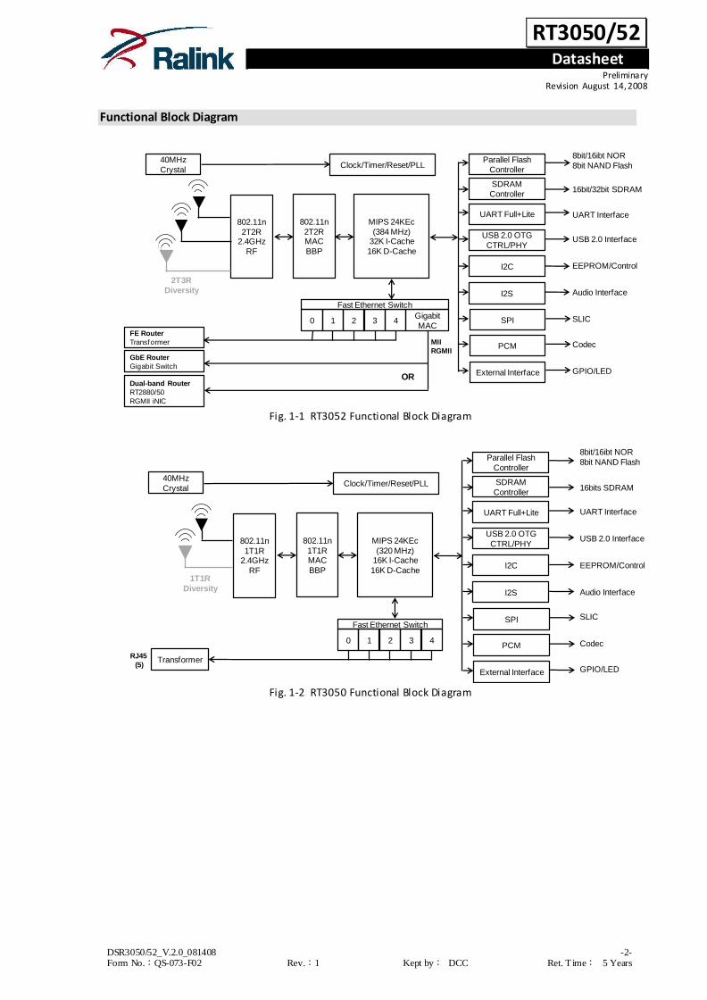
Functional Block Diagram
MIPS 24KEc
(384 MHz)32K I-Cache
16K D-Cache
Clock/Timer/Reset/PLL
802.11n
2T2RMAC
BBP
802.11n
2T2R2.4GHz
RF
2T3R
Diversity
Parallel Flash
Controller
SDRAM
Controller
PCM
SPI
I2S
I2C
USB 2.0 OTG
CTRL/PHY
UART Full+Lite
External Interface
40MHz
Crystal
FE Router
Transformer
8bit/16ibt NOR
8bit NAND Flash
16bit/32bit SDRAM
UART Interface
USB 2.0 Interface
EEPROM/Control
Audio Interface
SLIC
Codec
GPIO/LED
0 1 2 3 4Gigabit
MAC
Fast Ethernet Switch
GbE Router
Gigabit Switch
MII
RGMII
Dual-band Router
RT2880/50
RGMII iNIC
OR
Fig. 1-1 RT3052 Functional Block Diagram
8bit/16ibt NOR
8bit NAND Flash
16bits SDRAM
UART Interface
USB 2.0 Interface
EEPROM/Control
Audio Interface
SLIC
Codec
GPIO/LED
RJ45
(5)
MIPS 24KEc
(320 MHz)16K I-Cache
16K D-Cache
Clock/Timer/Reset/PLL
802.11n
1T1RMAC
BBP
802.11n
1T1R2.4GHz
RF1T1R
Diversity
Parallel Flash
Controller
SDRAM
Controller
0 1 2 3 4
Fast Ethernet Switch
PCM
SPI
I2S
I2C
USB 2.0 OTG
CTRL/PHY
UART Full+Lite
External Interface
40MHz
Crystal
Transformer
Fig. 1-2 RT3050 Functional Block Diagram

RT3050/52 Datasheet
Preliminary Revision August 14, 2008
DSR3050/52_V.2.0_081408 -3- Form No.:QS-073-F02 Rev.:1 Kept by: DCC Ret. T ime: 5 Years
Table of Content
1. Pin Description ..................................................................................................................7
1.1 289-Pins BGA Package Diagram ..................................................................................7
1.1.1 289-Pins BGA Package Diagram for RT3050F ...........................................................7
1.1.2 289-Pins BGA Package Diagram for RT3052F ...........................................................8
1.2 Pin Description ..........................................................................................................9
1.3 Pins Sharing Scheme ................................................................................................17
1.4 Boot strapping Signal description .............................................................................21
2. Maximum Ratings and Operating Conditions .....................................................................22
2.1 Absolute Maximum Ratings......................................................................................22
2.2 Thermal Information................................................................................................22
2.3 Operating Conditions ...............................................................................................22
2.4 Storage Condition ....................................................................................................22
2.5 DC Electrical Characteristics .....................................................................................22
2.6 AC Electrical Characteristics .....................................................................................23
2.6.1 SDRAM Interface .................................................................................................23
2.6.2 Flash/SRAM Interface ..........................................................................................24
2.6.3 RGMII Interface ...................................................................................................25
2.6.4 Power On Sequence ............................................................................................26
3. Function Description........................................................................................................27
3.1 Overview ................................................................................................................27
3.2 Memory Map Summary ...........................................................................................29
3.3 MIPS 24KEc Processor ..............................................................................................31
3.3.1 Features .............................................................................................................31
3.3.2 Block Diagram .....................................................................................................32
3.4 System Control ........................................................................................................33
3.4.1 Features .............................................................................................................33
3.4.2 Block Diagram .....................................................................................................33
3.4.3 Register Description (base: 0x1000.0000) ............................................................33
3.5 Timer ......................................................................................................................38
3.5.1 Features .............................................................................................................38
3.5.2 Block Diagram .....................................................................................................38
3.5.3 Register Description (base: 0x1000.0100) ............................................................38
3.6 Interrupt Controller .................................................................................................42
3.6.1 Features .............................................................................................................42
3.6.2 Block Diagram .....................................................................................................42
3.6.3 Register Description (base: 0x1000.0200) .............................................................42
3.7 UART ......................................................................................................................46
3.7.1 Features .............................................................................................................46
3.7.2 Loop-back control for communications link fault isolation Block Diagram ...............46
3.7.3 Register Description (base: 0x1000.0500) .............................................................46

RT3050/52 Datasheet
Preliminary Revision August 14, 2008
DSR3050/52_V.2.0_081408 -4- Form No.:QS-073-F02 Rev.:1 Kept by: DCC Ret. T ime: 5 Years
3.8 UART Lite ................................................................................................................52
3.8.1 Features .............................................................................................................52
3.8.2 Block Diagram .....................................................................................................52
3.8.3 Register Description (base: 0x1000.0C00) .............................................................52
3.9 Programmable I/O ...................................................................................................57
3.9.1 Features .............................................................................................................57
3.9.2 Block Diagram .....................................................................................................57
3.9.3 Register Description (base: 0x1000.0600) .............................................................57
3.10 I2C Controller ..........................................................................................................64
3.10.1 Features............................................................................................................64
3.10.2 Block Diagram ...................................................................................................64
3.10.3 Register Description (base: 0x1000.0900) ...........................................................64
3.11 SPI Controller ..........................................................................................................68
3.11.1 Features............................................................................................................68
3.11.2 Block Diagram ...................................................................................................68
3.11.3 Register Description (base: 0x1000.0B00) ...........................................................68
3.12 Generic DMA Controller ...........................................................................................71
3.12.1 Features............................................................................................................71
3.12.2 Block Diagram ...................................................................................................71
3.12.3 Register Description (base: 0x10000700) ............................................................71
3.13 PCM Controller ........................................................................................................75
3.13.1 Features............................................................................................................75
3.13.2 Block Diagram ...................................................................................................75
3.13.3 Register Description (base: 0x1000.0400) ...........................................................76
3.14 I2S Controller ..........................................................................................................80
3.14.1 Features............................................................................................................80
3.14.2 Block Diagram ...................................................................................................80
3.14.3 Register Description (base: 0x1000.0A00) ...........................................................81
3.15 Memory Controller ..................................................................................................83
3.15.1 Features............................................................................................................83
3.15.2 Block Diagram ...................................................................................................83
3.15.3 Register Description (base: 0x1000.0300) ...........................................................83
3.16 NAND Flash Controller .............................................................................................88
3.16.1 Features............................................................................................................88
3.16.2 Block Diagram ...................................................................................................88
3.16.3 Register Description (base: 0x1000.0800) ...........................................................88
3.17 Frame Engine ..........................................................................................................91
3.17.1 Features............................................................................................................91
3.17.2 Block Diagram ...................................................................................................92
3.17.3 Register Description (base: 0x1010.0000) ...........................................................95
3.18 Ethernet Switch ..................................................................................................... 111

RT3050/52 Datasheet
Preliminary Revision August 14, 2008
DSR3050/52_V.2.0_081408 -5- Form No.:QS-073-F02 Rev.:1 Kept by: DCC Ret. T ime: 5 Years
3.18.1 Features.......................................................................................................... 111
3.18.2 Block Diagram ................................................................................................. 112
3.18.3 Register Description (base: 0x1011.0000) ......................................................... 113
3.18.4 MII control register.......................................................................................... 127
3.19 USB OTG Controller & PHY ..................................................................................... 130
3.19.1 Features.......................................................................................................... 130
3.19.2 Block Diagram ................................................................................................. 130
3.19.3 Register Description (base: 0x101C.0000) ......................................................... 131
3.20 802.11n 2T2R MAC/BBP ......................................................................................... 180
3.20.1Features .......................................................................................................... 180
3.20.2Block Diagram .................................................................................................. 180
3.20.3Register Description (base: 0x1018.0000) ......................................................... 181
4. Package Physical Dimension ........................................................................................... 233
4.1 TFBGA 289B(14×14×0.94mm)............................................................................ 233
5. Revision History............................................................................................................. 235

RT3050/52 Datasheet
Preliminary Revision August 14, 2008
DSR3050/52_V.2.0_081408 -6- Form No.:QS-073-F02 Rev.:1 Kept by: DCC Ret. T ime: 5 Years
Table of Figures
Fig. 1-1 RT3052 Functional Block Diagram ......................................................................................... 2
Fig. 1-2 RT3050 Functional Block Diagram ......................................................................................... 2
Fig. 1-3-1 RT3052 MII MII PHY .................................................................................................... 18
Fig. 1-3-2 RT3052 RvMII MII MAC ............................................................................................... 19
Fig. 1-3-3 RT3052 RGMII RGMII PHY ........................................................................................... 19
Fig. 1-3-4 RT3052 RGMII RGMII MAC .......................................................................................... 20
Fig. 2-6-1 SDRAM Interface.............................................................................................................. 23
Fig. 2-6-2 Flash/SRAM Interface ...................................................................................................... 24
Fig. 2-6-3 RGMII Interface............................................................................................................... 25
Fig. 2-6-4 Power ON Sequence ........................................................................................................ 26
Fig. 3-1-1 RT3052 Block Diagram...................................................................................................... 27
Fig. 3-1-2 RT3050 Block Diagram...................................................................................................... 27
Fig. 3-3-1 MIPS 24KEc Processor Diagram......................................................................................... 32
Fig. 3-5-1 Timer Block Diagram ........................................................................................................ 38
Fig. 3-6-1 Interrupt Controller Block Diagram ................................................................................... 42
Fig. 3-7-1 UART Block Diagram......................................................................................................... 46
Fig. 3-8-1 UART Lite Block Diagram .................................................................................................. 52
Fig. 3-9-1 Program I/O Block Diagram .............................................................................................. 57
Fig. 3-10-1 I2C controller Block Diagram........................................................................................... 64
Fig. 3-11-1 SPI controller Block Diagram ........................................................................................... 68
Fig. 3-12-1 Generic DMA controller Block Diagram............................................................................ 71
Fig. 3-13-1 PCM Controller Block Diagram ........................................................................................ 75
Fig. 3-14-1 I2S Transmitter Block Diagram ........................................................................................ 80
Fig. 3-14-2 I2S Transmitter .............................................................................................................. 80
Fig. 3-15-1 Flash/SRAM/SDRAM controller Block Diagram ................................................................. 83
Fig. 3-15-2 Flash/SRAM/SDRAM Controller R/W waveform ............................................................... 85
Fig. 3-16-1 NAND Flash Controller Block Diagram ............................................................................. 88
Fig. 3-17-1 Frame Engine Block Diagram........................................................................................... 92
Fig. 3-17-2 PDMA FIFO-like Ring Concept ......................................................................................... 93
Fig. 3-17-3 PDMA TX Descriptor Format ........................................................................................... 94
Fig. 3-17-4 PDMA RX Descriptor Format ........................................................................................... 95
Fig. 3-18-1 Ethernet Switch Block Diagram ..................................................................................... 112
Fig. 3-19-1 1.1 USB OTG Controller & PHY Block Diagram ............................................................... 130
Fig. 3-20-1 802.11n 2T2R MAC/BBP Block Diagram ......................................................................... 180
Fig. 3-20-2 802.11n 2T2R MAC/BBP Register Map........................................................................... 181
Fig. 3-20-3 TX frame Information ................................................................................................... 223
Fig. 3-20-4 TX Descriptor Format ................................................................................................... 224
Fig. 3-20-5 TXWI Format................................................................................................................ 224
Fig. 3-20-6 RX Descriptor Ring........................................................................................................ 226
Fig. 3-20-7 RX Descriptor Format ................................................................................................... 226
Fig. 3-20-8 RXWI Format............................................................................................................... 227

RT3050/52 Datasheet
Preliminary Revision August 14, 2008
DSR3050/52_V.2.0_081408 -7- Form No.:QS-073-F02 Rev.:1 Kept by: DCC Ret. T ime: 5 Years
1. Pin Description
1.1 289-Pins BGA Package Diagram
1.1.1 289-Pins BGA Package Diagram for RT3050F
Top view (left portion) 1 2 3 4 5 6 7 8 9
A RF0_V12A RF0_2G_OUTP RF0_2G_INN RF0_2G_INP PLL_VC_CAP BG_RES_12K LDORF_OUT_V12RF_BB2_V12A ADC_VREFN
B NC GND RF_BB1_V12A VCO_VCO_V12A PLL_DIV_V12A LDOPLL_OUT_V12 LDORF_IN_VX RF0_TSSI_IN ADC_V12A
C NC RF1_V12A GND VCO_LO_V12A PLL_PRE_V12A PLL_X1 PLL_X2 BASE_TRX_IP BASE_TRX_QN
D NC RF0_PA_PE RF0_LO_V12A GND GND BG_V33A NC BASE_TRX_IN BASE_TRX_QP
E NC RF_V33A NC GND GND GND GND GND GND
F DSR_N TXD ANT_TRN WLAN_LED_N GND GND GND GND GND
G CTS_N RTS_N TXD2 ANT_TRNB GND GND GND GND GND
H UPHY_VDDA_V33A UPHY_VRES DCD_N RXD2 SOC_CO_V12D GND GND GND GND
J UPHY_PADP UPHY_PADM RXD DTR_N SOC_IO_V33D GND GND GND GND
K NC NC UPHY_VBUS RIN GND GND GND GND GND
L NC NC UPHY_ID UPHY_VDDL_V12D SOC_CO_V12D GND GND GND GND
M NC NC NC SOC_CO_V12D NC RGMII_IO_V33D RGMII_IO_V33D GND GND
N NC NC NC RGMII_IO_V33D RGMII_IO_V33D EPHY_V33A EPHY_V33A EPHY_V33A EPHY_V33A
P NC NC NC EPHY_REF_RES EPHY_LED3_N EPHY_LED4_N EPHY_LED0_N EPHY_V33A EPHY_V33A
R EPHY_RXN_p0 EPHY_RXP_p0 EPHY_TXP_p1 EPHY_TXN_p1 EPHY_TXP_p3 EPHY_TXN_p3 EPHY_LED1_N EPHY_LED2_N SPI_DIN
T EPHY_TXN_p0 EPHY_RXP_p1 EPHY_RXN_p2 EPHY_TXN_p2 EPHY_RXP_p3 EPHY_RXN_p4 EPHY_TXN_p4 PORST_N SPI_CLK
U EPHY_TXP_p0 EPHY_RXN_p1 EPHY_RXP_p2 EPHY_TXP_p2 EPHY_RXN_p3 EPHY_RXP_p4 EPHY_TXP_p4 SPI_DOUT SPI_EN
Top view (right portion) 10 11 12 13 14 15 16 17
ADC_VREFP ADC_VREF025P ADC_VREF LDODIG_OUT_V12 SRAM_CS_N MA20 MD1 MD6 A
ADC_V12D ADC_VREF025N NC OE_N FLASH_CS_N MD0 MD5 MD4 B
RF0_LNA_PE LDOADC_IN_VX LDODIG_IN_VX WE_N MA21 MD3 MD8 MD9 C
GND LDOADC_OUT_V12 LDO_V33A MA22 SOC_CO_V12D MD2 MD10 MD13 D
GND GND GND SOC_IO_V33D SOC_CO_V12D MD7 MD14 MD15 E
GND GND GND GND SOC_CO_V12D MD11 MA3 MA2 F
GND GND GND GND SOC_CO_V12D MD12 MA1 BPLL_VDD_V12D G
GND GND GND GND SOC_IO_V33D MA4 MA0 BPLL_POC_V33D H
GND GND GND GND SOC_IO_V33D BPLL_DVDD_V12D BPLL_DVDDA_V12D BPLL_AVDD_V12A J
GND GND GND GND SOC_IO_V33D MA5 MA7 MA6 K
GND GND GND GND SOC_IO_V33D SOC_CO_V12D MA9 MA8 L
GND GND GND SOC_IO_V33D SOC_IO_V33D MA15 MA11 MA10 M
SOC_IO_V33D SOC_IO_V33D SOC_IO_V33D SOC_IO_V33D NC MA19 MA13 MA14 N
SOC_CO_V12D SOC_CO_V12D NC NC NC NC MA18 MA12 P
I2C_SCLK JTAG_TDO NC NC NC NC SDRAM_CLK MA17 R
I2C_SD JTAG_TDI JTAG_TRST_N NC NC NC SDRAM_RAS_N MA16 T
GPIO0 JTAG_TMS JTAG_TCLK NC NC NC NC SDRAM_CS_N U
RT3050/52 Datasheet
Preliminary Revision August 14, 2008
DSR3050/52_V.2.0_081408 -8- Form No.:QS-073-F02 Rev.:1 Kept by: DCC Ret. T ime: 5 Years
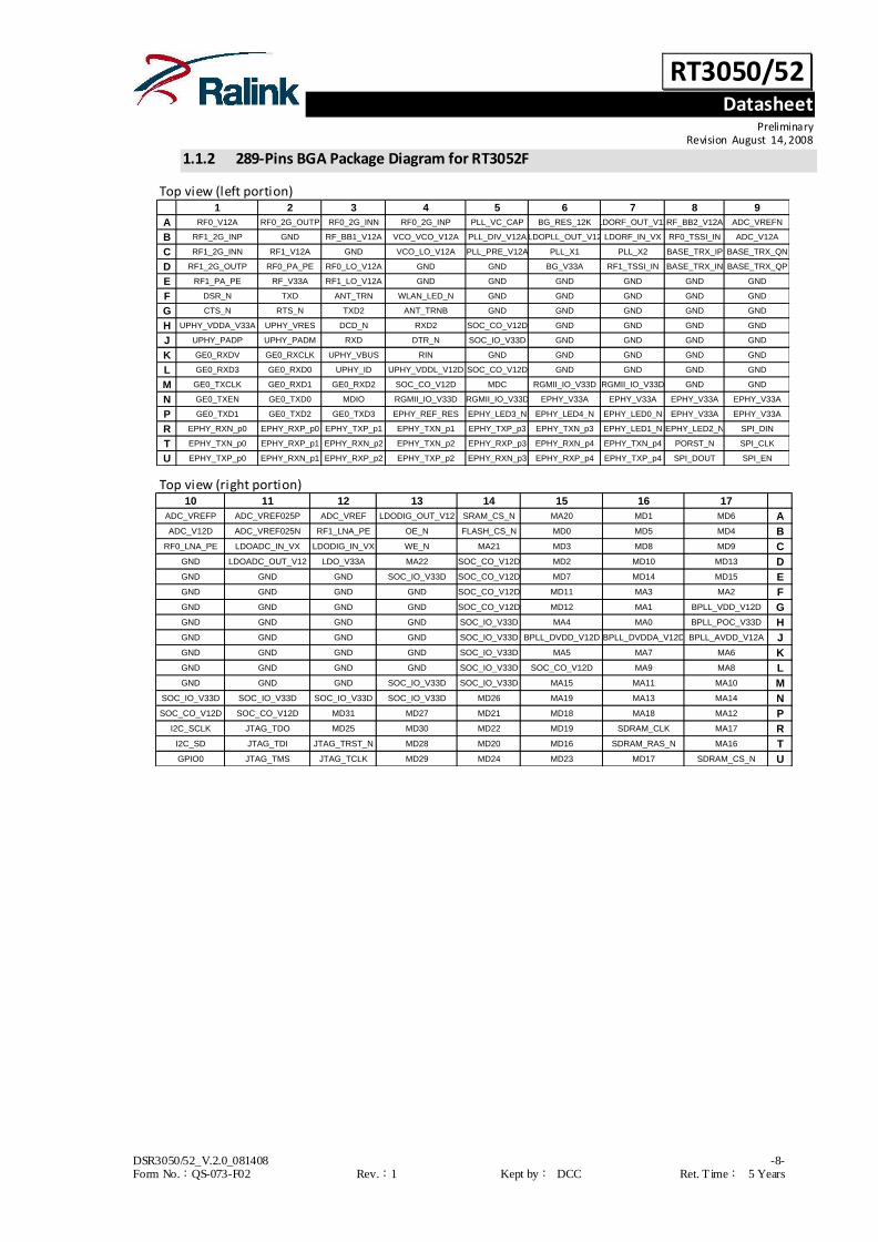
1.1.2 289-Pins BGA Package Diagram for RT3052F
Top view (left portion) 1 2 3 4 5 6 7 8 9
A RF0_V12A RF0_2G_OUTP RF0_2G_INN RF0_2G_INP PLL_VC_CAP BG_RES_12K LDORF_OUT_V12RF_BB2_V12A ADC_VREFN
B RF1_2G_INP GND RF_BB1_V12A VCO_VCO_V12A PLL_DIV_V12A LDOPLL_OUT_V12 LDORF_IN_VX RF0_TSSI_IN ADC_V12A
C RF1_2G_INN RF1_V12A GND VCO_LO_V12A PLL_PRE_V12A PLL_X1 PLL_X2 BASE_TRX_IP BASE_TRX_QN
D RF1_2G_OUTP RF0_PA_PE RF0_LO_V12A GND GND BG_V33A RF1_TSSI_IN BASE_TRX_IN BASE_TRX_QP
E RF1_PA_PE RF_V33A RF1_LO_V12A GND GND GND GND GND GND
F DSR_N TXD ANT_TRN WLAN_LED_N GND GND GND GND GND
G CTS_N RTS_N TXD2 ANT_TRNB GND GND GND GND GND
H UPHY_VDDA_V33A UPHY_VRES DCD_N RXD2 SOC_CO_V12D GND GND GND GND
J UPHY_PADP UPHY_PADM RXD DTR_N SOC_IO_V33D GND GND GND GND
K GE0_RXDV GE0_RXCLK UPHY_VBUS RIN GND GND GND GND GND
L GE0_RXD3 GE0_RXD0 UPHY_ID UPHY_VDDL_V12D SOC_CO_V12D GND GND GND GND
M GE0_TXCLK GE0_RXD1 GE0_RXD2 SOC_CO_V12D MDC RGMII_IO_V33D RGMII_IO_V33D GND GND
N GE0_TXEN GE0_TXD0 MDIO RGMII_IO_V33D RGMII_IO_V33D EPHY_V33A EPHY_V33A EPHY_V33A EPHY_V33A
P GE0_TXD1 GE0_TXD2 GE0_TXD3 EPHY_REF_RES EPHY_LED3_N EPHY_LED4_N EPHY_LED0_N EPHY_V33A EPHY_V33A
R EPHY_RXN_p0 EPHY_RXP_p0 EPHY_TXP_p1 EPHY_TXN_p1 EPHY_TXP_p3 EPHY_TXN_p3 EPHY_LED1_N EPHY_LED2_N SPI_DIN
T EPHY_TXN_p0 EPHY_RXP_p1 EPHY_RXN_p2 EPHY_TXN_p2 EPHY_RXP_p3 EPHY_RXN_p4 EPHY_TXN_p4 PORST_N SPI_CLK
U EPHY_TXP_p0 EPHY_RXN_p1 EPHY_RXP_p2 EPHY_TXP_p2 EPHY_RXN_p3 EPHY_RXP_p4 EPHY_TXP_p4 SPI_DOUT SPI_EN
Top view (right portion) 10 11 12 13 14 15 16 17
ADC_VREFP ADC_VREF025P ADC_VREF LDODIG_OUT_V12 SRAM_CS_N MA20 MD1 MD6 A
ADC_V12D ADC_VREF025N RF1_LNA_PE OE_N FLASH_CS_N MD0 MD5 MD4 B
RF0_LNA_PE LDOADC_IN_VX LDODIG_IN_VX WE_N MA21 MD3 MD8 MD9 C
GND LDOADC_OUT_V12 LDO_V33A MA22 SOC_CO_V12D MD2 MD10 MD13 D
GND GND GND SOC_IO_V33D SOC_CO_V12D MD7 MD14 MD15 E
GND GND GND GND SOC_CO_V12D MD11 MA3 MA2 F
GND GND GND GND SOC_CO_V12D MD12 MA1 BPLL_VDD_V12D G
GND GND GND GND SOC_IO_V33D MA4 MA0 BPLL_POC_V33D H
GND GND GND GND SOC_IO_V33D BPLL_DVDD_V12D BPLL_DVDDA_V12D BPLL_AVDD_V12A J
GND GND GND GND SOC_IO_V33D MA5 MA7 MA6 K
GND GND GND GND SOC_IO_V33D SOC_CO_V12D MA9 MA8 L
GND GND GND SOC_IO_V33D SOC_IO_V33D MA15 MA11 MA10 M
SOC_IO_V33D SOC_IO_V33D SOC_IO_V33D SOC_IO_V33D MD26 MA19 MA13 MA14 N
SOC_CO_V12D SOC_CO_V12D MD31 MD27 MD21 MD18 MA18 MA12 P
I2C_SCLK JTAG_TDO MD25 MD30 MD22 MD19 SDRAM_CLK MA17 R
I2C_SD JTAG_TDI JTAG_TRST_N MD28 MD20 MD16 SDRAM_RAS_N MA16 T
GPIO0 JTAG_TMS JTAG_TCLK MD29 MD24 MD23 MD17 SDRAM_CS_N U

RT3050/52 Datasheet
Preliminary Revision August 14, 2008
DSR3050/52_V.2.0_081408 -9- Form No.:QS-073-F02 Rev.:1 Kept by: DCC Ret. T ime: 5 Years
1.2 Pin Description
Pin Name I/O/IPU/IPD Description
JTAG interfaces : 5 pins
T12 JTAG_TRST_N I, IPU JTAG TRST.
U12 JTAG_TCLK I JTAG TCLK.
U11 JTAG_TMS I JTAG TMS.
T11 JTAG_TDI I JTAG TDI.
R11 JTAG_TDO O JTAG TDO.
UART Lite interface : 2 pins
H4 RXD2 I, IPD UART Lite RXD.
G3 TXD2 O UART Lite TXD.
UART Full interface : 8 pins
J3 RXD I, IPD UART RXD.
K4 RIN I UART RIN.
G1 CTS_N I UART CTS_N.
F1 DSR_N I UART DSR_N.
H3 DCD_N I UART DCD_N.
F2 TXD O UART TXD.
J4 DTR_N O UART DTR.
G2 RTS_N O UART RTS.
SPI interface : 4 pins
R9 SPI_DIN I SPI DIN.
U8 SPI_DOUT O SPI DOUT.
T9 SPI_CLK O SPI Clock.
U9 SPI_EN O SPI Data Enable.
I2C interface : 2 pins
R10 I2C_SCLK O, IPU I2C Clock.
T10 I2C_SD I/O, IPU I2C Data.
GPIO interface : 1 pin
U10 GPIO0 I/O When NAND-flash is applied, this pin should be used as the BUSY/READY pin. Otherwise, it is
dedicated as the GPIO0 Pin
Misc signals : 4 pins
T8 PORST_N I, IPU Power on reset
F4 WLAN_LED_N O WLAN Activity LED
F3 ANT_TRN O Positive signal for antenna T/R switch
G4 ANT_TRNB O Negative signal for antenna T/R switch
5-Port PHY : 26 pins
P4 EPHY_REF_RES I/O Connect to an external resistor to provide accurate bias current
R1 EPHY_RXN_P0 I 10/100 PHY Port #0 RXN
R2 EPHY _RXP_P0 I 10/100 PHY Port #0 RXP
T1 EPHY _TXN_P0 O 10/100 PHY Port #0 TXN
U1 EPHY _TXP_P0 O 10/100 PHY Port #0 TXP
U2 EPHY _RXN_P1 I 10/100 PHY Port #1 RXN
T2 EPHY _RXP_P1 I 10/100 PHY Port #1 RXP
R4 EPHY _TXN_P1 O 10/100 PHY Port #1 TXN
R3 EPHY _TXP_P1 O 10/100 PHY Port #1 TXP
T3 EPHY _RXN_P2 I 10/100 PHY Port #2 RXN
U3 EPHY _RXP_P2 I 10/100 PHY Port #2 RXP
T4 EPHY _TXN_P2 O 10/100 PHY Port #2 TXN
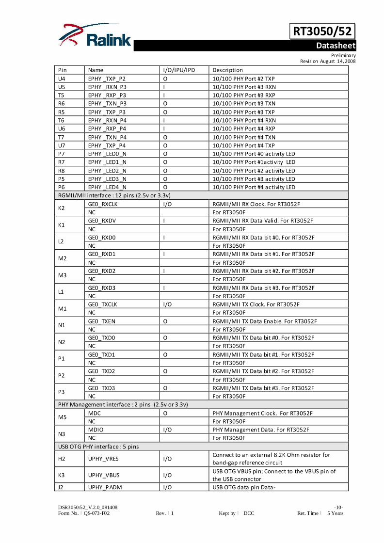
RT3050/52 Datasheet
Preliminary Revision August 14, 2008
DSR3050/52_V.2.0_081408 -10- Form No.:QS-073-F02 Rev.:1 Kept by: DCC Ret. T ime: 5 Years
Pin Name I/O/IPU/IPD Description
U4 EPHY _TXP_P2 O 10/100 PHY Port #2 TXP
U5 EPHY _RXN_P3 I 10/100 PHY Port #3 RXN
T5 EPHY _RXP_P3 I 10/100 PHY Port #3 RXP
R6 EPHY _TXN_P3 O 10/100 PHY Port #3 TXN
R5 EPHY _TXP_P3 O 10/100 PHY Port #3 TXP
T6 EPHY _RXN_P4 I 10/100 PHY Port #4 RXN
U6 EPHY _RXP_P4 I 10/100 PHY Port #4 RXP
T7 EPHY _TXN_P4 O 10/100 PHY Port #4 TXN
U7 EPHY _TXP_P4 O 10/100 PHY Port #4 TXP
P7 EPHY _LED0_N O 10/100 PHY Port #0 activity LED
R7 EPHY _LED1_N O 10/100 PHY Port #1activity LED
R8 EPHY _LED2_N O 10/100 PHY Port #2 activity LED
P5 EPHY _LED3_N O 10/100 PHY Port #3 activity LED
P6 EPHY _LED4_N O 10/100 PHY Port #4 activity LED
RGMII/MII interface : 12 pins (2.5v or 3.3v)
K2 GE0_RXCLK I/O RGMII/MII RX Clock. For RT3052F
NC For RT3050F
K1 GE0_RXDV I RGMII/MII RX Data Valid. For RT3052F
NC For RT3050F
L2 GE0_RXD0 I RGMII/MII RX Data bit #0. For RT3052F
NC For RT3050F
M2 GE0_RXD1 I RGMII/MII RX Data bit #1. For RT3052F
NC For RT3050F
M3 GE0_RXD2 I RGMII/MII RX Data bit #2. For RT3052F
NC For RT3050F
L1 GE0_RXD3 I RGMII/MII RX Data bit #3. For RT3052F
NC For RT3050F
M1 GE0_TXCLK I/O RGMII/MII TX Clock. For RT3052F
NC For RT3050F
N1 GE0_TXEN O RGMII/MII TX Data Enable. For RT3052F
NC For RT3050F
N2 GE0_TXD0 O RGMII/MII TX Data bit #0. For RT3052F
NC For RT3050F
P1 GE0_TXD1 O RGMII/MII TX Data bit #1. For RT3052F
NC For RT3050F
P2 GE0_TXD2 O RGMII/MII TX Data bit #2. For RT3052F
NC For RT3050F
P3 GE0_TXD3 O RGMII/MII TX Data bit #3. For RT3052F
NC For RT3050F
PHY Management interface : 2 pins (2.5v or 3.3v)
M5 MDC O PHY Management Clock. For RT3052F
NC For RT3050F
N3 MDIO I/O PHY Management Data. For RT3052F
NC For RT3050F
USB OTG PHY interface : 5 pins
H2 UPHY_VRES I/O Connect to an external 8.2K Ohm resistor for band-gap reference circuit
K3 UPHY_VBUS I/O USB OTG VBUS pin; Connect to the VBUS pin of the USB connec tor
J2 UPHY_PADM I/O USB OTG data pin Data-

RT3050/52 Datasheet
Preliminary Revision August 14, 2008
DSR3050/52_V.2.0_081408 -11- Form No.:QS-073-F02 Rev.:1 Kept by: DCC Ret. T ime: 5 Years
Pin Name I/O/IPU/IPD Description
J1 UPHY_PADP I/O USB OTG data pin Data+
L3 UPHY_ID I/O USB OTG ID pin. Connect to ID pin on the Mini -type connec t
SDRAM/Flash/SRAM Interface : 62pins
P12 MD31 I/O SDRAM/Flash/SRAM Data bit #31 for RT3052F
NC For RT3050F
R13 MD30 I/O SDRAM/Flash/SRAM Data bit #30 for RT3052F
NC For RT3050F
U13 MD29 I/O SDRAM/Flash/SRAM Data bit #29 for RT3052F
NC For RT3050F
T13 MD28 I/O SDRAM/Flash/SRAM Data bit #28 for RT3052F
NC For RT3050F
P13 MD27 I/O SDRAM/Flash/SRAM Data bit #27 for RT3052F
NC For RT3050F
N14 MD26 I/O SDRAM/Flash/SRAM Data bit #26 for RT3052F
NC For RT3050F
R12 MD25 I/O SDRAM/Flash/SRAM Data bit #25 for RT3052F
NC For RT3050F
U14 MD24 I/O SDRAM/Flash/SRAM Data bit #24 for RT3052F
NC For RT3050F
U15 MD23 I/O SDRAM/Flash/SRAM Data bit #23 for RT3052F
NC For RT3050F
R14 MD22 I/O SDRAM/Flash/SRAM Data bit #22 for RT3052F
NC For RT3050F
P14 MD21 I/O SDRAM/Flash/SRAM Data bit #21 for RT3052F
NC For RT3050F
T14 MD20 I/O SDRAM/Flash/SRAM Data bit #20 for RT3052F
NC For RT3050F
R15 MD19 I/O SDRAM/Flash/SRAM Data bit #19 for RT3052F
NC For RT3050F
P15 MD18 I/O SDRAM/Flash/SRAM Data bit #18 for RT3052F
NC For RT3050F
U16 MD17 I/O SDRAM/Flash/SRAM Data bit #17 for RT3052F
NC For RT3050F
T15 MD16 I/O SDRAM/Flash/SRAM Data bit #16 for RT3052F
NC For RT3050F
E17 MD15 I/O SDRAM/Flash/SRAM Data bit #15
E16 MD14 I/O SDRAM/Flash/SRAM Data bit #14
D17 MD13 I/O SDRAM/Flash/SRAM Data bit #13
G15 MD12 I/O SDRAM/Flash/SRAM Data bit #12
F15 MD11 I/O SDRAM/Flash/SRAM Data bit #11
D16 MD10 I/O SDRAM/Flash/SRAM Data bit #10
C17 MD9 I/O SDRAM/Flash/SRAM Data bit #9
C16 MD8 I/O SDRAM/Flash/SRAM Data bit #8
E15 MD7 I/O SDRAM/NAND or NOR Flash/SRAM Data bit #7
A17 MD6 I/O SDRAM/NAND or NOR Flash/SRAM Data bit #6
B16 MD5 I/O SDRAM/NAND or NOR Flash/SRAM Data bit #5
B17 MD4 I/O SDRAM/NAND or NOR Flash/SRAM Data bit #4
C15 MD3 I/O SDRAM/NAND or NOR Flash/SRAM Data bit #3
D15 MD2 I/O SDRAM/NAND or NOR Flash/SRAM Data bit #2

RT3050/52 Datasheet
Preliminary Revision August 14, 2008
DSR3050/52_V.2.0_081408 -12- Form No.:QS-073-F02 Rev.:1 Kept by: DCC Ret. T ime: 5 Years
Pin Name I/O/IPU/IPD Description
A16 MD1 I/O SDRAM/NAND or NOR Flash/SRAM Data bit #1
B15 MD0 I/O SDRAM/NAND or NOR Flash/SRAM Data bit #0
D13 MA22 I/O Flash/SRAM Address bit #22 This pin is shared with NAND flash CLE
C14 MA21 I/O Flash/SRAM Address bit #21 This pin is shared with NAND flash RE_N
A15 MA20 I/O, IPD Flash/SRAM Address bit #20
This pin is shared with NAND flash WE_N
N15 MA19 I/O,IPD Flash/SRAM Address bit #19 or SDRAM DQM bit#3
P16 MA18 I/O, IPD Flash/SRAM Address bit #18 or SDRAM DQM bit#2
R17 MA17 I/O , IPU Flash/SRAM Address bit #17 or SDRAM DQM bit#1
T17 MA16 I/O , IPD Flash/SRAM Address bit #16 or SDRAM DQM bit#0
M15 MA15 I/O , IPU Flash/SRAM Address bit #15 or SDRAM BA bit#1
N17 MA14 I/O , IPU Flash/SRAM Address bit #14 or SDRAM BA bit#0
N16 MA13 I/O , IPD SDRAM/Flash/SRAM Address bit #13
This pin is shared with NAND flash ALE
P17 MA12 I/O , IPD SDRAM/Flash/SRAM Address bit #12
M16 MA11 I/O , IPD SDRAM/Flash/SRAM Address bit #11
M17 MA10 I/O , IPD SDRAM/Flash/SRAM Address bit #10
L16 MA9 I/O , IPD SDRAM/Flash/SRAM Address bit #9
L17 MA8 I/O , IPD SDRAM/Flash/SRAM Address bit #8
K16 MA7 I/O , IPD SDRAM/Flash/SRAM Address bit #7
K17 MA6 I/O , IPD SDRAM/Flash/SRAM Address bit #6
K15 MA5 I/O , IPD SDRAM/Flash/SRAM Address bit #5
H15 MA4 I/O , IPD SDRAM/Flash/SRAM Address bit #4
F16 MA3 I/O , IPD SDRAM/Flash/SRAM Address bit #3
F17 MA2 I/O , IPD SDRAM/Flash/SRAM Address bit #2
G16 MA1 I/O , IPD SDRAM/Flash/SRAM Address bit #1
H16 MA0 I/O , IPD SDRAM/Flash/SRAM Address bit #0
T16 SDRAM_RAS_N O SDRAM Row Address Select
U17 SDRAM_CS_N O SDRAM Chip Select
R16 SDRAM_CLK O SDRAM Clock
C13 WE_N O Flash/SRAM Write Enable and SDRAM Write
Enable (SDRAM_WE_N)
B13 OE_N O Flash/SRAM Write Output Enable and SDRAM Column Address Select (SDRAM_CAS_N)
B14 FLASH_CS_N O Flash Chip Select or NAND Flash CS_N if boot from NAND is selected.
A14 SRAM_CS_N O SRAM Chip Select
RF interface, related LDO and power pins : 47 pins
A4 RF0_2G_INP I 2.4GHz RX0 input (positive)
A3 RF0_2G_INN I 2.4GHz RX0 input (negative)
A2 RF0_2G_OUTP O 2.4GHz TX0 output (positive)
B1 RF1_2G_INP I 2.4GHz RX1 input (positive) for RT3052F
NC For RT3050F
C1 RF1_2G_INN I 2.4GHz RX1 input (negative)
NC For RT3050F
D1 RF1_2G_OUTP O 2.4GHz TX1 output (positive) for RT3052F
NC For RT3050F
D2 RF0_PA_PE O 0~3.3V control for external PA0 (20mA)

RT3050/52 Datasheet
Preliminary Revision August 14, 2008
DSR3050/52_V.2.0_081408 -13- Form No.:QS-073-F02 Rev.:1 Kept by: DCC Ret. T ime: 5 Years
Pin Name I/O/IPU/IPD Description
E1 RF1_PA_PE O
0~3.3V control for external PA1 (20mA) for RT3052F
NC For RT3050F
C10 RF0_LNA_PE O External LNA0 3.3V power (50mA)
B12 RF1_LNA_PE O External LNA1 3.3V power (50mA) for RT3052F
NC For RT3050F
B8 RF0_TSSI_IN I TX signal strength monitor input0 (0 ~3.3V)
D7 RF1_TSSI_IN I
TX signal strength monitor input1 (0 ~3.3V) for RT3052F
NC For RT3050F
B3 RF_BB1_V12A P 1.2V Supply for analog baseband
A8 RF_BB2_V12A P 1.2V Supply for analog baseband
D3 RF0_LO_V12A P 1.2V Supply for LO & IF
E3 RF1_LO_V12A P 1.2V Supply for LO & IF
A1 RF0_V12A P 1.2V Supply for RF channel 0
C2 RF1_V12A P 1.2V Supply for RF channel 1
E2 RF_V33A P 3.3V supply for PA Enable drivers (40mA)
B4 VCO_VCO_V12A P 1.2V Supply for VCO core
A5 PLL_VC_CAP I/O PLL external loop filter
B10 ADC_V12D P 1.2V supply for ADC digital logics
A12 ADC_VREF I/O Main ADC referenc e voltage
A11 ADC_VREF025P I/O Auxiliary ADC reference voltage (p)
B11 ADC_VREF025N I/O Auxiliary ADC reference voltage (n)
B9 ADC_V12A P 1.2V supply for ADC analog blocks
A10 ADC_VREFP O Auxiliary ADC reference voltage (p)
A9 ADC_VREFN O Auxiliary ADC reference voltage (n)
C9 BASE_TRX_QN I/O Baseband Q 20Mhz debug I/O (negative)
D9 BASE_TRX_QP I/O Baseband Q 20Mhz debug I/O (postive)
D8 BASE_TRX_IN I/O Baseband I 20Mhz debug I/O (negative)
C8 BASE_TRX_IP I/O Baseband I 20Mhz debug I/O (postive)
C12 LDODIG_IN_VX I LDO 1.5-2.0V 600mA input
D12 LDO_V33A P 3.3V supply for LDOs
A13 LDODIG_OUT_V12 O LDO 1.2V 600mA output for digital core
C11 LDOADC_IN_VX I LDO 1.5-2V 200mA input for ADC
D11 LDOADC_OUT_V12 O LDO 1.2V 200mA output for ADC
B7 LDORF_IN_VX I LDO 1.5~2V 300mA input for RF core and PLL
A7 LDORF_OUT_V12 O LDO 1.2V 200mA output for RF core
B6 LDOPLL_OUT_V12 O LDO 1.2V 50mA output for RF PLL
A6 BG_RES_12K I/O External reference resistor (12K ohm)
D6 BG_V33A P 3.3V supply for band gap reference
C6 PLL_X1 I Crystal oscillator input
C7 PLL_X2 O Crystal oscillator output
B5 PLL_DIV_V12A P 1.2V Supply for PLL divider
C5 PLL_PRE_V12A P 1.2V Supply for PLL prescaler
C4 VCO_LO_V12A P 1.2V Supply for VCO output buffer
Other power pins : 39 pins
J15 BPLL_DVDD_V12D P 1.2v PLL digital power supply
J16 BPLL_DVDDA_V12D P 1.2v PLL digital power supply
J17 BPLL_AVDD_V12A P 1.2v PLL analog power supply
H17 BPLL_POC_V33D P 3.3v PLL digital power supply

RT3050/52 Datasheet
Preliminary Revision August 14, 2008
DSR3050/52_V.2.0_081408 -14- Form No.:QS-073-F02 Rev.:1 Kept by: DCC Ret. T ime: 5 Years
Pin Name I/O/IPU/IPD Description
G17 BPLL_VDD_V12D P 1.2v PLL digital power supply
N6 EPHY_V33A P 3.3v 10/100 PHY analog power supply
N7 EPHY_V33 A P 3.3v 10/100 PHY analog power supply
N8 EPHY_V33A P 3.3v 10/100 PHY analog power supply
N9 EPHY_V33A P 3.3v 10/100 PHY analog power supply
P8 EPHY_V33A P 3.3v 10/100 PHY analog power supply
P9 EPHY_V33A P 3.3v 10/100 PHY analog power supply
N4 RGMII_IO_V33D P 2.5v/3.3v RGMII I/O power supply
N5 RGMII_IO_V33D P 2.5v/3.3v RGMII I/O power supply
M6 RGMII_IO_V33D P 2.5v/3.3v RGMII I/O power supply
M7 RGMII_IO_V33D P 2.5v/3.3v RGMII I/O power supply
H1 UPHY_VDDA_V33A P 3.3v USB PHY analog power suppl y
L4 UPHY_VDDL_V12D P 1.2v USB PHY digital power supply
J5 SOC_IO_V33D P 3.3v digital I/O power supply
M4 SOC_CO_V12D P 1.2v digital core power supply
H5 SOC_CO_V12D P 1.2v digital core power supply
L5 SOC_CO_V12D P 1.2v digital core power supply
P10 SOC_CO_V12D P 1.2v digital core power supply
P11 SOC_CO_V12D P 1.2v digital core power supply
D14 SOC_CO_V12D P 1.2v digital core power supply
E14 SOC_CO_V12D P 1.2v digital core power supply
F14 SOC_CO_V12D P 1.2v digital core power supply
G14 SOC_CO_V12D P 1.2v digital core power supply
L15 SOC_CO_V12D P 1.2v digital core power supply
E13 SOC_IO_V33D P 3.3v digital I/O power supply
H14 SOC_IO_V33D P 3.3v digital I/O power supply
J14 SOC_IO_V33D P 3.3v digital I/O power supply
K14 SOC_IO_V33D P 3.3v digital I/O power supply
L14 SOC_IO_V33D P 3.3v digital I/O power supply
M14 SOC_IO_V33D P 3.3v digital I/O power supply
N10 SOC_IO_V33D P 3.3v digital I/O power supply
N11 SOC_IO_V33D P 3.3v digital I/O power supply
N12 SOC_IO_V33D P 3.3v digital I/O power supply
N13 SOC_IO_V33D P 3.3v digital I/O power supply
M13 SOC_IO_V33D P 3.3v digital I/O power supply
Ground pins : 70 pins
B2 GND P Ground pin
C3 GND P Ground pin
D4 GND P Ground pin
D5 GND P Ground pin
D10 GND P Ground pin
E4 GND P Ground pin
E5 GND P Ground pin
E6 GND P Ground pin
E7 GND P Ground pin
E8 GND P Ground pin
E9 GND P Ground pin
E10 GND P Ground pin
E11 GND P Ground pin

RT3050/52 Datasheet
Preliminary Revision August 14, 2008
DSR3050/52_V.2.0_081408 -15- Form No.:QS-073-F02 Rev.:1 Kept by: DCC Ret. T ime: 5 Years
Pin Name I/O/IPU/IPD Description
E12 GND P Ground pin
F5 GND P Ground pin
F6 GND P Ground pin
F7 GND P Ground pin
F8 GND P Ground pin
F9 GND P Ground pin
F10 GND P Ground pin
F11 GND P Ground pin
F12 GND P Ground pin
F13 GND P Ground pin
G5 GND P Ground pin
G6 GND P Ground pin
G7 GND P Ground pin
G8 GND P Ground pin
G9 GND P Ground pin
G10 GND P Ground pin
G11 GND P Ground pin
G12 GND P Ground pin
G13 GND P Ground pin
H6 GND P Ground pin
H7 GND P Ground pin
H8 GND P Ground pin
H9 GND P Ground pin
H10 GND P Ground pin
H11 GND P Ground pin
H12 GND P Ground pin
H13 GND P Ground pin
J6 GND P Ground pin
J7 GND P Ground pin
J8 GND P Ground pin
J9 GND P Ground pin
J10 GND P Ground pin
J11 GND P Ground pin
J12 GND P Ground pin
J13 GND P Ground pin
K5 GND P Ground pin
K6 GND P Ground pin
K7 GND P Ground pin
K8 GND P Ground pin
K9 GND P Ground pin
K10 GND P Ground pin
K11 GND P Ground pin
K12 GND P Ground pin
K13 GND P Ground pin
L6 GND P Ground pin
L7 GND P Ground pin
L8 GND P Ground pin
L9 GND P Ground pin
L10 GND P Ground pin

RT3050/52 Datasheet
Preliminary Revision August 14, 2008
DSR3050/52_V.2.0_081408 -16- Form No.:QS-073-F02 Rev.:1 Kept by: DCC Ret. T ime: 5 Years
Pin Name I/O/IPU/IPD Description
L11 GND P Ground pin
L12 GND P Ground pin
L13 GND P Ground pin
M8 GND P Ground pin
M9 GND P Ground pin
M10 GND P Ground pin
M11 GND P Ground pin
M12 GND P Ground pin
Total: 289 pins
*Note: IPD means internal pull -down; IPU means internal pull -up; P means power.

RT3050/52 Datasheet
Preliminary Revision August 14, 2008
DSR3050/52_V.2.0_081408 -17- Form No.:QS-073-F02 Rev.:1 Kept by: DCC Ret. T ime: 5 Years
1.3 Pins Sharing Scheme
Some pins are shared with GPIO to provide maximum flexibility for system designers. The RT3050/52
provides up to 52(RT3052)/22(RT3050) GPIO pins. Users can configure SYSCFG and GPIOMODE registers in
the System Control block to specify the pin function. Unless it specified explicitly, all the GPIO pins are in
input mode after reset.
RGMII_GPIO_MODE description
Pin Name RGMII_GPIO_MODE=0 RGMII_GPIO_MODE=1
GE0_RXCLK GE0_RXCLK GPIO51
GE0_RXDV GE0_RXDV GPIO50
GE0_RXD0 GE0_RXD0 GPIO49
GE0_RXD1 GE0_RXD1 GPIO48
GE0_RXD2 GE0_RXD2 GPIO47
GE0_RXD3 GE0_RXD3 GPIO46
GE0_TXCLK GE0_TXCLK GPIO45
GE0_TXEN GE0_TXEN GPIO44
GE0_TXD0 GE0_TXD0 GPIO43 GE0_TXD1 GE0_TXD1 GPIO42
GE0_TXD2 GE0_TXD2 GPIO41
GE0_TXD3 GE0_TXD3 GPIO40
SDRAM_GPIO_MODE description
Pin Name SDRAM_GPIO_MODE=0 SDRAM_GPIO_MODE=1
{MD31:MD16} {MD31:MD16} GPIO39~GPIO24
MDIO_GPIO_MODE description
Pin Name MDIO_GPIO_MODE=0 MDIO_GPIO_MODE=1
MDC MDC GPIO23
MDIO MDIO GPIO22
JTAG_GPIO_MODE description
Pin Name JTAG_GPIO_MODE=0 JTAG_GPIO_MODE=1
JTAG_TRST_N JTAG_TRST_N GPIO21
JTAG_TCLK JTAG_TCLK GPIO20
JTAG_TMS JTAG_TMS GPIO19
JTAG_TDI JTAG_TDI GPIO18
JTAG_TDO JTAG_TDO GPIO17
UARTL_GPIO_MODE description
Pin Name UARTL_GPIO_MODE=0 UARTL_GPIO_MODE=1
RXD2 RXD2 GPIO16
TXD2 TXD2 GPIO15
UARTF_SHARE_MODE description
Pin Name
3’b000 UARTF
3’b001 PCM, UARTF
3’b010 PCM, I2S
3’b011 I2S UARTF
3’b100 PCM, GPIO
3’b101 GPIO, UARTF
3’b110 GPIO I2S
3’b111 GPIO
RIN RIN PCMDTX PCMDTX RXD PCMDTX GPIO14 GPIO14 GPIO14
DSR_N DSR_N PCMDRX PCMDRX CTS_N PCMDRX GPIO13 GPIO13 GPIO13
DCD_N DCD_N PCMCLK PCMCLK TXD PCMCLK GPIO12 GPIO12 GPIO12
DTR_N DTR_N PCMFS PCMFS RTS_N PCMFS GPIO11 GPIO11 GPIO11
RXD RXD RXD REFCLK REFCLK REFCLK RXD REFCLK GPIO10
CTS_N CTS_N CTS_N I2SSD I2SSD GPIO9 CTS_N I2SSD GPIO9
TXD TXD TXD I2SWS I2SWS GPIO8 TXD I2SWS GPIO8
RTS_N RTS_N RTS_N I2SCLK I2SCLK GPIO7 RTS_N I2SCLK GPIO7

RT3050/52 Datasheet
Preliminary Revision August 14, 2008
DSR3050/52_V.2.0_081408 -18- Form No.:QS-073-F02 Rev.:1 Kept by: DCC Ret. T ime: 5 Years
SPI_GPIO_MODE description
Pin Name SPI_GPIO_MODE=0 SPI_GPIO_MODE=1
SPI_DIN SPI_DIN GPIO6
SPI_DOUT SPI_DOUT GPIO5
SPI_CLK SPI_CLK GPIO4 SPI_EN SPI_EN GPIO3
I2C_GPIO_MODE description
Pin Name I2C_gpio_mode=0 I2C_gpio_mode=1
I2C_SCLK I2C_SCLK GPIO2
I2C_SD I2C_SD GPIO1
Notes :
1. All given GPIOs are 4mA drive capable.
2. The default direction for GPIO pins are input(i.e. tri -state) except the GPIO pins (GPIO17…GPIO21) s hared
with the JTAG interface. The default value for JTAG_GPIO_MODE is 1.
3. MII, RvMII and RGMII Interfacing Scenarios:
a. RT3052 supports MII/RvMII (Reversed MII) for 10/100Mbps mode and RGMII for
10/100/1000Mbps mode. The operation mode is determined by boot strapping settings (please
refer to the GE0_MODE in the next session).
i . For example, when GE0_MODE is set to 2’b10, reserved MII mode is configured during
the boot strapping. In this mode, TXCLK becomes an output and TXD [3:0]/TXCTL
become inputs; RXCLK becomes an output and RXD [3:0]/RXCTL become outputs.
Please refer to the following application scenarios for better understanding.
RT3052 MII
TXCLK
RXCLK
TXCTL/TXEN
TXD[3:0]
RXCTL/RXDV
RXD[3:0]
MDC
MDIO
MII PHY
MII
GE0_TXCLK
GE0_RXCLK
GE0_TXCTL
GE0_TXD[3:0]
GE0_RXCTL
GE0_RXD[3:0]
MDC
MDIO
Fig. 1-3-1 RT3052 MII MII PHY

RT3050/52 Datasheet
Preliminary Revision August 14, 2008
DSR3050/52_V.2.0_081408 -19- Form No.:QS-073-F02 Rev.:1 Kept by: DCC Ret. T ime: 5 Years
GE0_TXCLK
GE0_RXCLK
GE0_TXCTL
GE0_TXD[3:0]
GE0_RXCTL
GE0_RXD[3:0]
MDC
MDIO
RT3052 RvMII
TXCLK
RXCLK
TXCTL/TXEN
TXD[3:0]
RXCTL/RXDV
RXD[3:0]
MDC
MDIO
MII MAC
RvMII
Fig. 1-3-2 RT3052 RvMII MII MAC
RT3052 RGMII
TXCLK
RXCLK
TXCTL/TXEN
TXD[3:0]
RXCTL/RXDV
RXD[3:0]
MDC
MDIO
RGMII PHY
RGMII
GE0_TXCLK
GE0_RXCLK
GE0_TXCTL
GE0_TXD[3:0]
GE0_RXCTL
GE0_RXD[3:0]
MDC
MDIO
Fig. 1-3-3 RT3052 RGMII RGMII PHY

RT3050/52 Datasheet
Preliminary Revision August 14, 2008
DSR3050/52_V.2.0_081408 -20- Form No.:QS-073-F02 Rev.:1 Kept by: DCC Ret. T ime: 5 Years
RT3052 RGMII
TXCLK
RXCLK
TXCTL/TXEN
TXD[3:0]
RXCTL/RXDV
RXD[3:0]
RGMII MAC
RGMII
GE0_TXCLK
GE0_RXCLK
GE0_TXCTL
GE0_TXD[3:0]
GE0_RXCTL
GE0_RXD[3:0]
MDC
MDIO
MDC
MDIO
Fig. 1-3-4 RT3052 RGMII RGMII MAC

RT3050/52 Datasheet
Preliminary Revision August 14, 2008
DSR3050/52_V.2.0_081408 -21- Form No.:QS-073-F02 Rev.:1 Kept by: DCC Ret. T ime: 5 Years
1.4 Boot strapping Signal description
Pin Name Boot Strapping Signal Name
Description
MA7..MA0 TEST_CODE[7:0] A vec tor to set CHIP operation/testing modes. In normal operation, please use the default value :
8’b00000000
{MA9, MA8} BOOT_FROM 2’b00 : boot from external 16-bit flash (default) 2’b01 : boot from external 8-bit flash 2’b10 : boot from external NAND flash 2’b11 : boot from internal ROM
MA10 CPU_CLK_SEL 1’b0 : Low (320Mhz)
1’b1 : High (384Mhz, default)
MA12 BIG_ENDIAN 0 : Little Endian (default) 1 : Big Endian
MA13 BYPASS_PLL 0 : Do Not Bypass PLL (default) 1: Bypass PLL
MA14 BOOT_ADDR 0 : CPU boots at address 0x1FC00000(default)
1 : CPU boots at address 0x1F000000
{MA17,MA16} GE_MODE Gigabit Port Mode 2’b00 : RGMII Mode (10/100/1000M bps)
2’b01 : MII Mode (10/100 Mbps) 2’b10 : Reversed MII Mode (10/100 Mbps) 2’b11 : Reserve
MA20 INIC_8MB_SDRAM 0 : INIC SDRAM size is 2MB (default) 1 : INIC SDRAM size is 8MB
MA21 INIC_EE_SDRAM 0 : Take INIC SDRAM size from INIC_8MB setting (default)
1 : Take INIC SDRAM size from EEPROM

RT3050/52 Datasheet
Preliminary Revision August 14, 2008
DSR3050/52_V.2.0_081408 -22- Form No.:QS-073-F02 Rev.:1 Kept by: DCC Ret. T ime: 5 Years
2. Maximum Ratings and Operating Conditions
2.1 Absolute Maximum Ratings
Supply Voltage …………………………..…….……………………………………………..…………..… .…………………………… ..….….3.6V
Vcc to Vcc Decouple………………………………………………………………….……………………….………… .…….….. –0.3 to +0.3V
Input, Output or I/O Voltage……..…………………………………..……………………………………...... GND –0.3V to Vcc+0.3V
2.2 Thermal Information
Thermal Resistance θJA (oC/W) in free air for TFBGA (14x14mm) package………………….… ...…….…32.5°C /W
Thermal Resistance θJC (oC/W) in free air for TFBGA (14x14mm) package……….…………..…… ..…….… 6°C /W
Maximum Junction Temperature (Plastic Package) ……….......…………….……..............…… .…… ..…… .…………125°C
Maximum Lead Temp erature (Soldering 10s)………………..……… ..…….....….......……………………….....……….. 300°C
2.3 Operating Conditions
Temperature Range ………………………………....……... ..… ......………..……………………………… ..………........ -10 to 55°C
Core Supply Voltage………………………......……....…….……………… .…………………………...…… ..………….…… 1.2V +/- 5%
I/O Supply Voltage …………………….…………………….......……......………………………….………… ......………. 3.3V +/- 10%
2.4 Storage Condition
The calculated shelf life in sealed bag is 12 months if stored between 0°C and 40°C at less than 90% relative
humidity (RH). After the bag is opened, devices that are subjected to solder reflow or other high temperature
processes must be handled in the following manner: a) Mounted within 168-hours of factory conditions < 30°C /60%RH
b) Storage humidity needs to maintained at <10% RH
c) Backing is necessary if customer expose the component to air over 168 hrs, backing condition: 125°C /
8hrs
2.5 DC Electrical Characteristics
Parameters Sym Conditions Min Typ Max Unit
3.3V Supply Voltage Vcc33 3.0 3.3 3.6 V
1.2V Supply Voltage Vcc12 1.14 1.2 1.26 V
3.3V Current Consumption Icc33 217 mA mA
1.5V Current Consumption Icc12 656 mA mA
2.0V Current Consumption (@transformer center tap)
Icc20 514 mA mA
RT3050/52 Datasheet
Preliminary Revision August 14, 2008
DSR3050/52_V.2.0_081408 -23- Form No.:QS-073-F02 Rev.:1 Kept by: DCC Ret. T ime: 5 Years
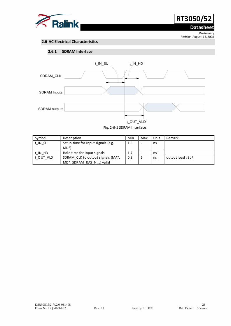
2.6 AC Electrical Characteristics
2.6.1 SDRAM Interface
SDRAM_CLK
SDRAM Inputs
SDRAM outputs
t_IN_SU t_IN_HD
t_OUT_VLD
Fig. 2-6-1 SDRAM Interface
Symbol Description Min Max Unit Remark
t_IN_SU Setup time for Input signals (e.g.
MD*)
1.5 - ns
t_IN_HD Hold time for input signals 1.7 - ns t_OUT_VLD SDRAM_CLK to output signals (MA*,
MD*, SDRAM_RAS_N,…) valid
0.8 5 ns output load : 8pF
RT3050/52 Datasheet
Preliminary Revision August 14, 2008
DSR3050/52_V.2.0_081408 -24- Form No.:QS-073-F02 Rev.:1 Kept by: DCC Ret. T ime: 5 Years
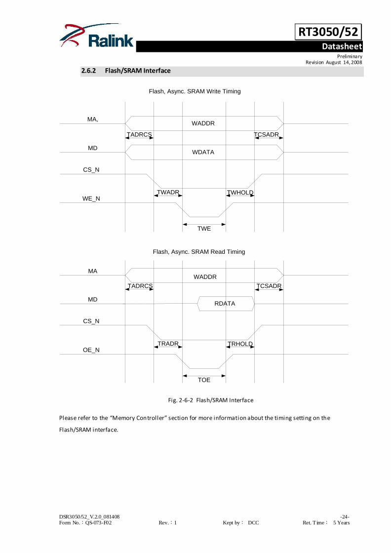
2.6.2 Flash/SRAM Interface
MD
CS_N
WE_N
TADRCS
TWADR
TWE
TWHOLD
TCSADR
MD
CS_N
OE_N
TADRCS
TRADR
TOE
TRHOLD
TCSADR
MA,
WDATA
WADDR
MAWADDR
RDATA
Flash, Async. SRAM Write Timing
Flash, Async. SRAM Read Timing
Fig. 2-6-2 Flash/SRAM Interface
Please refer to the “Memory Controller” section for more information about the timing setting on the
Flash/SRAM interface.
RT3050/52 Datasheet
Preliminary Revision August 14, 2008
DSR3050/52_V.2.0_081408 -25- Form No.:QS-073-F02 Rev.:1 Kept by: DCC Ret. T ime: 5 Years
2.6.3 RGMII Interface
GE0_TXCLK
GE0_TXD/TXCTL
t_TX_SU
t_TX_HD
GE0_RXCLK
GE0_RXD/RXCTL
t_RX_SU
t_RX_HD
Fig. 2-6-3 RGMII Interface
Symbol Description Min Max Unit Remark
t_TX_SU Setup time for output signals (e.g.
GE0_TXD*, GE0_TXEN)
1.2 - ns output load : 5pF
t_TX_HD Hold time for output signals 1.2 - ns output load : 5pF
t_RX_SU Setup time for input signals (e.g. GE0_RXD*, GE0_RXDV)
1.0 - ns
t_RX_HD Hold time for input signals 1.0 - ns
RT3050/52 Datasheet
Preliminary Revision August 14, 2008
DSR3050/52_V.2.0_081408 -26- Form No.:QS-073-F02 Rev.:1 Kept by: DCC Ret. T ime: 5 Years
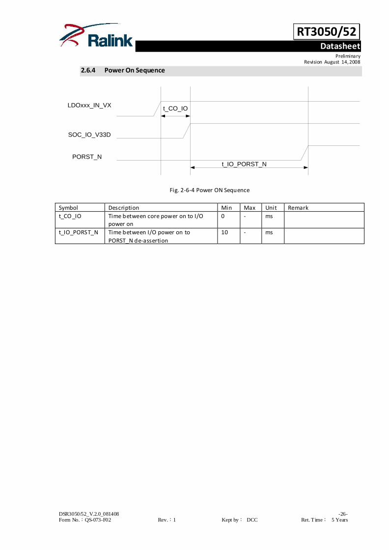
2.6.4 Power On Sequence
LDOxxx_IN_VX
SOC_IO_V33D
PORST_N
t_CO_IO
t_IO_PORST_N
Fig. 2-6-4 Power ON Sequence
Symbol Description Min Max Unit Remark
t_CO_IO Time between core power on to I/O power on
0 - ms
t_IO_PORST_N Time between I/O power on to
PORST_N de-assertion
10 - ms

RT3050/52 Datasheet
Preliminary Revision August 14, 2008
DSR3050/52_V.2.0_081408 -27- Form No.:QS-073-F02 Rev.:1 Kept by: DCC Ret. T ime: 5 Years
3. Function Description
3.1 Overview
The RT3050/52 SOC combines Ralink’s 802.11n compliant 2T2R MAC/BBP/RF, a high performance 384 -MHz
MIPS24KEc CPU core, USB OTG controller/PHY, and 5(FE)+1(GE) port Ethernet switch and a 5 -port
10/100Mbps Ethernet PHY , to enable a multitude of high performance, cost-effective 802.11n applications.
MIPS 24KEc
(384 MHz)32K I-Cache
16K D-Cache
Clock/Timer/Reset/PLL
802.11n
2T2RMAC
BBP
802.11n
2T2R2.4GHz
RF
2T3R
Diversity
Parallel Flash
Controller
SDRAM
Controller
PCM
SPI
I2S
I2C
USB 2.0 OTG
CTRL/PHY
UART Full+Lite
External Interface
40MHz
Crystal
FE Router
Transformer
8bit/16ibt NOR
8bit NAND Flash
16bit/32bit SDRAM
UART Interface
USB 2.0 Interface
EEPROM/Control
Audio Interface
SLIC
Codec
GPIO/LED
0 1 2 3 4Gigabit
MAC
Fast Ethernet Switch
GbE Router
Gigabit Switch
MII
RGMII
Dual-band Router
RT2880/50
RGMII iNIC
OR
Fig. 3-1-1 RT3052 Block Diagram
8bit/16ibt NOR
8bit NAND Flash
16bits SDRAM
UART Interface
USB 2.0 Interface
EEPROM/Control
Audio Interface
SLIC
Codec
GPIO/LED
RJ45
(5)
MIPS 24KEc
(320 MHz)16K I-Cache
16K D-Cache
Clock/Timer/Reset/PLL
802.11n
1T1RMAC
BBP
802.11n
1T1R2.4GHz
RF1T1R
Diversity
Parallel Flash
Controller
SDRAM
Controller
0 1 2 3 4
Fast Ethernet Switch
PCM
SPI
I2S
I2C
USB 2.0 OTG
CTRL/PHY
UART Full+Lite
External Interface
40MHz
Crystal
Transformer
Fig. 3-1-2 RT3050 Block Diagram

RT3050/52 Datasheet
Preliminary Revision August 14, 2008
DSR3050/52_V.2.0_081408 -28- Form No.:QS-073-F02 Rev.:1 Kept by: DCC Ret. T ime: 5 Years
There are 4 bus masters (MIPS 24KEc, Ethernet Switch, USB OTG, and 802.11n MAC/BBP/RF) in the RT3050/52
SoC on a high performance, low latency Rbus, (Ralink Bus). In addition, the RT3050/52 SoC supports lower speed
peripherals such as UART, Timer, GPIO, I2C, SPI, I2S and PCM via a low speed peripheral bus (Pbus).The
Flash/SRAM/SDRAM controller is the only bus slave on the Rbus. It includes an Advanced Memory Scheduler to
arbitrate the requests from bus masters, enhancing the performance of memory access intensive tasks such as
AP/Router packet processing.
The RT3052 has an embedded 5(FE)+1(GE) port Ethernet switch and a 5-port 10/100. Besides the normal L2
switch function, it also embeds Ralink’s patent pending packet processing engine (PPE) to offload AP/Router
packet forwarding tasks such as firewall, NAT, NAPT and layer 2 bridging from the MIPS CPU. It also features a
high performance PDMA (packet DMA) which not only sorts and retrieves packets to and from the SDRAM but
also supports CPU offloading packet functions such as IP/TCP/UDP checksum checking/generation, PPPoE session
ID insertion and VLAN tag insertion. Ralink’s packet processing engine technology enables the RT3052 to perform
at the level of higher MHz CPU’s.
The RT3050/52 SoC embeds Ralink’s market proven 802.11n 2T2R MAC/BBP/RF to provide a 300Mbps PHY rate
on the wireless LAN interface. The MAC design employs a highly efficient DMA engine and hardware data
processing accelerators, which free the CPU for user applications. The 802.11n 2T2R MAC/BBP/RF is designed to
support standards based features in the area of security, quality of service and international regulation resulting
in an enhanced end user experience.

RT3050/52 Datasheet
Preliminary Revision August 14, 2008
DSR3050/52_V.2.0_081408 -29- Form No.:QS-073-F02 Rev.:1 Kept by: DCC Ret. T ime: 5 Years
3.2 Memory Map Summary
Start End Size Description
0000.0000 - 03FF.FFFF 64M SDRAM
0400.0000 - 0FFF.FFFF <<Reserved>>
1000.0000 - 1000.00FF 256 SYSCTL
1000.0100 - 1000.01FF 256 TIMER
1000.0200 - 1000.02FF 256 INTCTL
1000.0300 - 1000.03FF 256 MEM_CTRL (SDRAM & Flash/SRAM)
1000.0400 - 1000.04FF 256 PCM
1000.0500 - 1000.05FF 256 UART
1000.0600 - 1000.06FF 256 PIO
1000.0700 - 1000.07FF 256 Generic DMA
1000.0800 - 1000.08FF 256 NAND Flash Controller
1000.0900 - 1000.09FF 256 I2C
1000.0A00 - 1000.0AFF 256 I2S
1000.0B00 - 1000.0BFF 256 SPI
1000.0C00 - 1000.0CFF 256 UARTLITE
1000.0D00 - 100F.FFFF <<Reserved>>
1010.0000 - 1010.FFFF 64K Frame Engine
1011.0000 - 1011.7FFF 32K Ethernet Switch
1011.8000 1011.9FFF 8K ROM
1011_a000 1011_FFFF <<Reserved>>
1012.0000 - 1012.7FFF 32K <<Reserved>>
1012.8000 1012.FFFF 32K <<Reserved>>
1013.0000 - 1013.7FFF 32K <<Reserved>>
1013.8000 - 1013.FFFF 32K <<Reserved>>
1014.0000 - 1017.FFFF 256K <<Reserved>>
1018.0000 - 101B.FFFF 256K 802.11n MAC/BBP
101C.0000 - 101F.FFFF 256K USB OTG
1020.0000 - 1AFF.FFFF <<Reserved>>
1B00.0000 - 1BFF.FFFF 16MB External SRAM/Flash
1C00.0000 - 1EFF.FFFF <<Reserved>>
1F00.0000 - 1FFF.FFFF
16MB(flash) or 4KB(ram)
or 8KB(rom)
When BOOT_FROM = 2’b00,
up-to 16MB external 16-bit flash is mapped.
When BOOT_FROM = 2’b01,
up-to 8MB external 8-bit flash is mapped.
When BOOT_FROM = 2’b10,
4KB internal boot RAM is mapped for boot from NAND application.
When BOOT_FROM = 2’b11, 8KB internal boot ROM is mapped for iNIC application.
Note :
When boot from NAND option is enabled (set boot strapping signal: BOOT_FROM = 2’b10), the accessing to the
external flash will be remapped to the i nternal 4KB boot SRAM located in USB OTG (0x101E_0000 – 0x101E_3FFF). Accesses to original flash memory region outside of the 4KB boot SRAM are invalid in this boot from NAND mode. The 4KB SRAM is also accessible from 0x101E_0000 – 0x101E_3FFF memory space.

RT3050/52 Datasheet
Preliminary Revision August 14, 2008
DSR3050/52_V.2.0_081408 -30- Form No.:QS-073-F02 Rev.:1 Kept by: DCC Ret. T ime: 5 Years
When the boot from ROM option is enabled (set boot strapping signal: BOOT_FROM = 2’b11), the accessing to
the external flash will be remapped to the internal 8KB boot ROM located in (0x1011_8000 – 0x1011_9FFF).
Accesses to original flash memory region outside of the 8KB boot ROM is invalid in this boot from ROM mode.
The 8KB ROM is also accessible from 0x1011_8000 – 0x1011_9FFF memory space.

RT3050/52 Datasheet
Preliminary Revision August 14, 2008
DSR3050/52_V.2.0_081408 -31- Form No.:QS-073-F02 Rev.:1 Kept by: DCC Ret. T ime: 5 Years
3.3 MIPS 24KEc Processor
3.3.1 Features
8-stage pipeline
32-bit address paths
64-bit data paths to caches and external interface
MIPS32-Compatible Instruction Set
Multiply-Accumulate and Multiply-Subtract Instructions (MADD, MADDU, MSUB, MSUBU)
Targeted Multiply Instruction (MUL)
Zero/One Detect Instructions (CLZ, CLO)
Wait Instruction (WAIT)
Conditional Move Instructions (MOVZ, MOVN)
Prefetch Instruction (PREF)
MIPS32 Enhanced Architecture (Release 2) Features
Vectored interrupts and support for external interrupt controller
Programmable exception vector base
Atomic interrupt enable/disable
GPR shadow registers (optionally, one or three additional shadows can be added to minimize latency
for interrupt handlers)
Bit field manipulation instructions
MIPS32 Privileged Resource Architecture
MIPS DSP ASE
Fractional data types (Q15, Q31)
Saturating arithmetic
SIMD instructions operate on 2x16b or 4x8b simultaneously
3 additional pairs of accumulator registers
Programmable Memory Management Unit
32 dual-entry JTLB with variable page sizes
4-entry ITLB
8-entry DTLB
Optional simple Fixed Mapping Translation (FMT) mechanism
MIPS16e™ Code Compression
16 bit encodings of 32 bit instructions to improve code density
Special PC-relative instructions for efficient loading of addresses and constants
SAVE & RESTORE macro instructions for setting up and tearing down stack fra mes within
subroutines
Improved support for handling 8 and 16 bit datatypes
Programmable L1 Cache Sizes
Instruction cache size : 32KB
Data cache size : 16KB
4-Way Set Associative
Up to 8 outstanding load misses
Write-back and write-through support
32-byte cache line size
RT3050/52 Datasheet
Preliminary Revision August 14, 2008
DSR3050/52_V.2.0_081408 -32- Form No.:QS-073-F02 Rev.:1 Kept by: DCC Ret. T ime: 5 Years
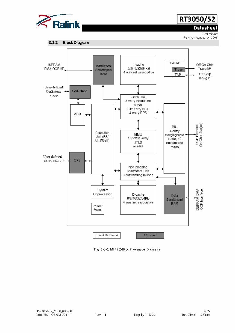
3.3.2 Block Diagram
Fig. 3-3-1 MIPS 24KEc Processor Diagram

RT3050/52 Datasheet
Preliminary Revision August 14, 2008
DSR3050/52_V.2.0_081408 -33- Form No.:QS-073-F02 Rev.:1 Kept by: DCC Ret. T ime: 5 Years
3.4 System Control
3.4.1 Features
Provide read-only chip revision registers
Provide a window to access boot-strapping signals
Support memory remapping configurations
Support software reset to each platform building block
Provide registers to determine GPIO and other peripheral pin muxing schemes
Provide some power-on-reset only test registers for software programmers
Combine miscellaneous registers (such as clock skew control, status register, memo registers,…etc)
3.4.2 Block Diagram
PalmBus Interface
System Ctrl Registers
Boot Strapping Signals GPIO Pin Muxing Scheme
Memory RemapingCPU Rbus Wrapper
Pin Muxing Block
Platform blocksPer Block S/W Reset
Cache Hit/Miss Strobes
Some Misc. registersPPCI, PCM, ...
System Control Block
To/From MIPS
Fig. 3-4-1 System Control Block Diagram
3.4.3 Register Description (base: 0x1000.0000)
CHIPID0_3: Chip ID ASCII Character 0-3 (offset: 0x00)
Bits Type Name Description Initial value
31:24 RO CHIP_ID3 ASCII CHIP Name Identification Character 3 8’h30 (‘0’)
23:16 RO CHIP_ID2 ASCII CHIP Name Identification Character 2 8’h 33 (‘3’)
15:8 RO CHIP_ID1 ASCII CHIP Name Identification Character 1 8’h 54 (‘T’)
7:0 RO CHIP_ID0 ASCII CHIP Name Identification Character 0 8’h 52 (‘R’)
CHIPID4_7: Chip Name ASCII Character 4-7 (offset: 0x04)
Bits Type Name Description Initial value
31:24 RO CHIP_ID7 ASCII CHIP Name Identification Character 7 8’h 20 (‘ ‘) 23:16 RO CHIP_ID6 ASCII CHIP Name Identification Character 6 8’h 20 (‘ ’)
15:8 RO CHIP_ID5 ASCII CHIP Name Identification Character 5 8’h 32 (‘2’)
7:0 RO CHIP_ID4 ASCII CHIP Name Identification Character 4 8’h 35 (‘5’)
SYSCFG: System Configuration Register (offset: 0x10)
Bits Type Name Description Initial value
31:30 - - Reserved 2’b0
29 RO INIC_EE_SDRAM 0: Don’t care EEPROM SDRAM configuration for iNIC 1: Take SDRAM configuration for iNIC form EEPROM if
available Bootstrap

RT3050/52 Datasheet
Preliminary Revision August 14, 2008
DSR3050/52_V.2.0_081408 -34- Form No.:QS-073-F02 Rev.:1 Kept by: DCC Ret. T ime: 5 Years
Note: There is no special H/W function related to the setting of this bit. That means the firmware could use it for
other purposes (as a general purpose bootstrapping).
28 RO INIC_8MB_SDRAM
0: SDRAM configuration is 2MB for iNIC
1: SDRAM configuration is 8MB for iNIC Note : There is no special H/W function related to the setting of this bit. That means the firmware could use it for
other purposes (as a general purpose bootstrapping).
Bootstrap
27:26 - - Reserved 2’b0
25:24 RO GE0_MODE
Gigabit Port Mode
2’b00 : RGMII Mode (10/100/1000M bps) 2’b01 : MII Mode (10/100 Mbps) 2’b10 : Reversed MI I Mode (10/100 Mbps)
2’b11 : Reserved
2’b00
23 - - Reserved 1’b0
22 RO BOOT_ADDR 0 : CPU boots at address 0x1FC00000
1 : CPU boots at address 0x1F000000 1’b0
21 RO- BYPASS_PLL 0: Not bypass PLL 1: Bypass PLL
Bootstrap
20 RO BIG_ENDIAN 0: Little endian 1: Big endian
Bootstrap
19 - - Reserved 1’b0
18 RO CPU_CLK_SEL 0: 320Mhz 1: 384 Mhz
Note : System clock is 1/3 of the CPU CLK
Bootstrap
17:16 RO BOOT_FROM
2’b00 : boot from external 16-bit flash (default) 2’b01 : boot from external 8-bit flash 2’b10 : boot from external NAND flash 2’b11 : boot from internal ROM
Bootstrap
15:8 R/W TEST_CODE[7:0]
Probe signals selection
Default value is from bootstrap and can by modify by software
Bootstrap
7:4 - - Reserved 7’b0
3:2 WO SRAM_CS_MODE
2’b00: Normal SRAM chip select output (active low) 2’b01: Watch dog reset output (active low for 3 system clocks)
2’b10: BT coexistence signal “WLAN_ACT” output 2’b11: Reserved.
Note : These two bits are write only. The read value is always 2’b00.
2’b00
1 - - Reserved 1’b0
0 WO SDRAM_CLK_DRV
1’b0 : 8mA SDRAM_CLK driving 1’b1 : 12mA SDRAM_CLK driving
Note : This bit is write only. The read value is always 1’b0.
1’b0
Reserved register (offset: 0x14)
Bits Type Name Description Initial value
31:0 - - Reserved 32’b0
TESTSTAT: Firmware Test Status Register (offset: 0x18)
Bits Type Name Description Initial value
31:0 R/W TSETSTAT[31:0] Firmware Test Status Note: This register is reset only by power on reset.
32’b0

RT3050/52 Datasheet
Preliminary Revision August 14, 2008
DSR3050/52_V.2.0_081408 -35- Form No.:QS-073-F02 Rev.:1 Kept by: DCC Ret. T ime: 5 Years
TESTSTAT2:Firmware Test Status Register 2 (offset: 0x1C)
Bits Type Name Description Initial value
31:0 R/W TSETSTAT2[31:0] Firmware Test Status 2 Note: This register is reset only by power on reset.
32’b0
Reserved register (offset: 0x20)
Bits Type Name Description Initial value
31:0 - - Reserved 32’b0
Reserved register (offset: 0x24)
Bits Type Name Description Initial value
31:0 - - Reserved 32’b0
Reserved register (offset: 0x28)
Bits Type Name Description Initial value
31:0 - - Reserved 32’b0
CLKCFG0: Clock Configuration Register 0 (offset: 0x2C)
Bits Type Name Description Initial value
31:30 R/W SDRAM_CLK_SKEW
0 : zero delay 1: delay 1ns 2 : delay 2ns 3 : delay 3ns
2’b01
29:0 - - Reserved 30’b0
CLKCFG1: Clock Configuration Register 1 (offset: 0x30)
Bits Type Name Description Initial value
31 - - Reserved 1’b0
30 R/W PBUS_DIV2 0 : Pbus clock is running at the same frequency as System
clock 1 : Pbus clock is running at 1/2 frequency of System clock
1’b0
29:19 - - Reserved 11’b0
18 R/W OTG_CLK_EN 0 : USB OTG clock is gated
1 : USB OTG clock is enabled 1’b1
17:16 - - Reserved 2’b0
15 R/W I2S_CLK_EN 0 : I2S clock is gated 1 : I2S clock is enabled
1’b0
14 R/W I2S_CLK_SEL I2S reference select 1’b0 : internal 15.625Mhz reference clock 1’b1 : external reference clock
1’b0
13:8 R/W I2S_CLK_DIV
I2S clock divider The source of this divider comes from two sources. One is
from REF_CLK (see 2.2 Pin sharing scheme-UARTF share mode ) and the other is from internal 15.625 Mhz reference clock.
The I2S clock divider will divide the referenc e clock by (I2S_CLK_DIV+1). The final I2S_CLK is obtained from the divided reference clock or external REF_CLK clock, depending on I2S_CLK_SEL
setting.
6’h28
7 R/W PCM_CLK_EN 0 : PCM clock is gated 1 : PCM clock is enabled
1’b0
6 R/W PCM_CLK_SEL PCM reference select 1’b0 : internal 15.625Mhz reference clock 1’b1 : external reference clock
1’b0
RT3050/52 Datasheet
Preliminary Revision August 14, 2008
DSR3050/52_V.2.0_081408 -36- Form No.:QS-073-F02 Rev.:1 Kept by: DCC Ret. T ime: 5 Years
5:0 R/W PCM_CLK_DIV
PCM clock divider The source of this divider comes from two places. One is
from REF_CLK (see 2.2 Pin sharing scheme-UARTF share mode) and the other is from internal 15.625Mhz reference clock. The PCM clock divider will divide the referenc e clock by
(PCM_CLK_DIV+1). The final PCM_CLK is obtained from the divided reference clock or external REF_CLK clock depending on the PCM_CLK_SEL setting.
6’h3c
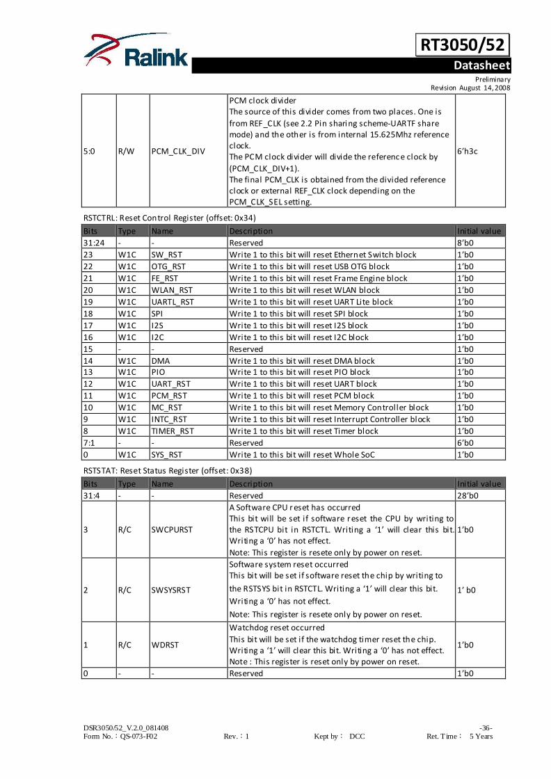
RSTCTRL: Reset Control Register (offset: 0x34)
Bits Type Name Description Initial value
31:24 - - Reserved 8’b0
23 W1C SW_RST Write 1 to this bit will reset Ethernet Switch block 1’b0
22 W1C OTG_RST Write 1 to this bit will reset USB OTG block 1’b0
21 W1C FE_RST Write 1 to this bit will reset Frame Engine block 1’b0
20 W1C WLAN_RST Write 1 to this bit will reset WLAN block 1’b0
19 W1C UARTL_RST Write 1 to this bit will reset UART Lite block 1’b0
18 W1C SPI Write 1 to this bit will reset SPI block 1’b0
17 W1C I2S Write 1 to this bit will reset I2S block 1’b0
16 W1C I2C Write 1 to this bit will reset I2C block 1’b0
15 - - Reserved 1’b0
14 W1C DMA Write 1 to this bit will reset DMA block 1’b0 13 W1C PIO Write 1 to this bit will reset PIO block 1’b0
12 W1C UART_RST Write 1 to this bit will reset UART block 1’b0
11 W1C PCM_RST Write 1 to this bit will reset PCM block 1’b0
10 W1C MC_RST Write 1 to this bit will reset Memory Controller block 1’b0
9 W1C INTC_RST Write 1 to this bit will reset Interrupt Controller block 1’b0
8 W1C TIMER_RST Write 1 to this bit will reset Timer block 1’b0
7:1 - - Reserved 6’b0
0 W1C SYS_RST Write 1 to this bit will reset Whole SoC 1’b0
RSTSTAT: Reset Status Register (offset: 0x38)
Bits Type Name Description Initial value
31:4 - - Reserved 28’b0
3 R/C SWCPURST
A Software CPU reset has occurred This bit will be set if software reset the CPU by writing to the RSTCPU bit in RSTCTL. Writing a ‘1’ will clear this bit. Writing a ‘0’ has not effect.
Note: This register is resete only by power on reset.
1’b0
2 R/C SWSYSRST
Software system reset occurred This bit will be set if software reset the chip by writing to
the RSTSYS bit in RSTCTL. Writing a ‘1’ will clear this bit.
Writing a ‘0’ has not effect.
Note: This register is resete only by power on reset.
1’ b0
1 R/C WDRST
Watchdog reset occurred
This bit will be set if the watchdog timer reset the chip. Writing a ‘1’ will clear this bit. Writing a ‘0’ has not effect. Note : This register is reset only by power on reset.
1’b0
0 - - Reserved 1’b0
RT3050/52 Datasheet
Preliminary Revision August 14, 2008
DSR3050/52_V.2.0_081408 -37- Form No.:QS-073-F02 Rev.:1 Kept by: DCC Ret. T ime: 5 Years
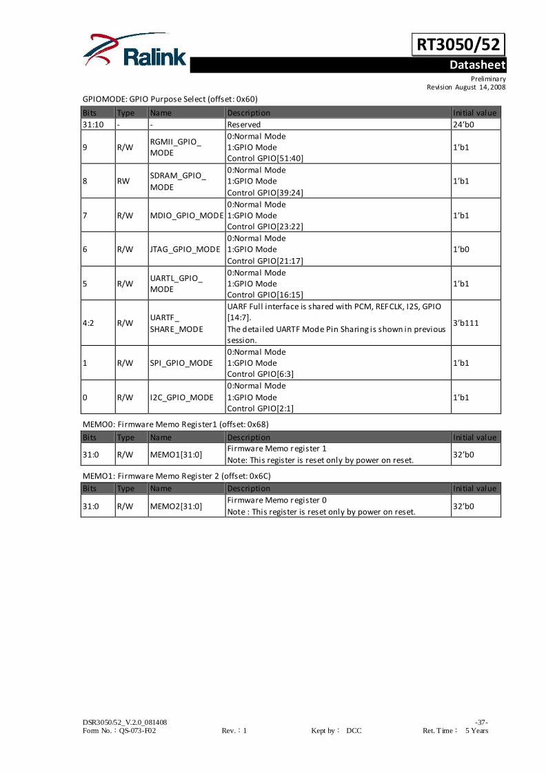
GPIOMODE: GPIO Purpose Select (offset: 0x60)
Bits Type Name Description Initial value
31:10 - - Reserved 24’b0
9 R/W RGMII_GPIO_ MODE
0:Normal Mode 1:GPIO Mode Control GPIO[51:40]
1’b1
8 RW SDRAM_GPIO_
MODE
0:Normal Mode 1:GPIO Mode
Control GPIO[39:24]
1’b1
7 R/W MDIO_GPIO_MODE 0:Normal Mode 1:GPIO Mode Control GPIO[23:22]
1’b1
6 R/W JTAG_GPIO_MODE 0:Normal Mode 1:GPIO Mode
Control GPIO[21:17]
1’b0
5 R/W UARTL_GPIO_ MODE
0:Normal Mode 1:GPIO Mode Control GPIO[16:15]
1’b1
4:2 R/W UARTF_
SHARE_MODE
UARF Full interface is shared with PCM, REFCLK, I2S, GPIO [14:7].
The detailed UARTF Mode Pin Sharing is shown in previous session.
3’b111
1 R/W SPI_GPIO_MODE 0:Normal Mode 1:GPIO Mode Control GPIO[6:3]
1’b1
0 R/W I2C_GPIO_MODE
0:Normal Mode
1:GPIO Mode Control GPIO[2:1]
1’b1
MEMO0: Firmware Memo Register1 (offset: 0x68)
Bits Type Name Description Initial value
31:0 R/W MEMO1[31:0] Firmware Memo register 1
Note: This register is reset only by power on reset. 32’b0
MEMO1: Firmware Memo Register 2 (offset: 0x6C)
Bits Type Name Description Initial value
31:0 R/W MEMO2[31:0] Firmware Memo register 0
Note : This register is reset only by power on reset. 32’b0

RT3050/52 Datasheet
Preliminary Revision August 14, 2008
DSR3050/52_V.2.0_081408 -38- Form No.:QS-073-F02 Rev.:1 Kept by: DCC Ret. T ime: 5 Years
3.5 Timer
3.5.1 Features
Independent clock pre-scale for each timer
Independent interrupts for each timer
Two General-purpose timers
Periodic mode
Free-running mode
Time-out mode
Second timer may be used as watchdog timer
Watchdog timer resets system on time-out
3.5.2 Block Diagram
Fig. 3-5-1 Timer Block Diagram
3.5.3 Register Description (base: 0x1000.0100)
TMRSTAT: Timer Status Register (offset: 0x00)
Bits Type Name Description Initial value
31:6 - - Reserved 26’b0
5 W TMR1RST
Timer 1 Reset Writing a ‘1’ to this bit will reset the Timer 1 to 0xFFFF if in
free-running mode, or the value specified in the TMR1LOAD
register in all other modes.
Writing a ‘0’ to this bit has no effect. Reading this bit will return a ‘0’.
1’b0
4 W TMR0RST
Timer 0 Reset
Writing a ‘1’ to this bit will reset Timer 0 to 0xFFFF if in free-running mode, or the value specified in the
1’b0
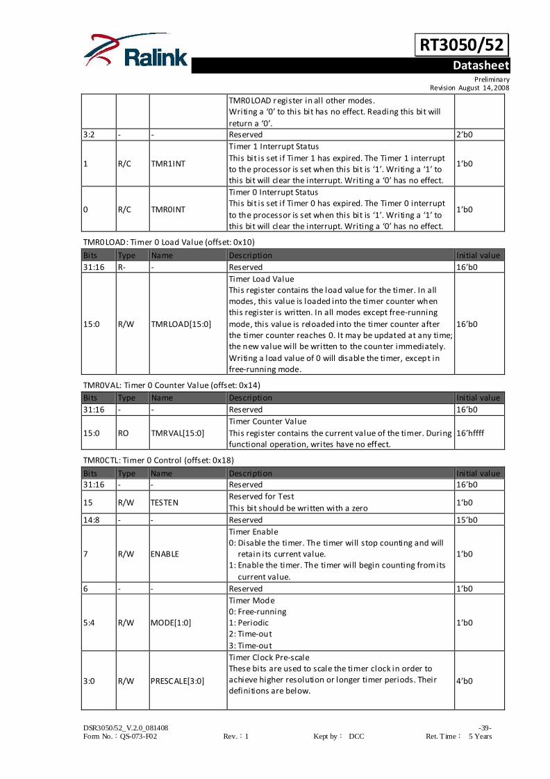
RT3050/52 Datasheet
Preliminary Revision August 14, 2008
DSR3050/52_V.2.0_081408 -39- Form No.:QS-073-F02 Rev.:1 Kept by: DCC Ret. T ime: 5 Years
TMR0LOAD register in all other modes. Writing a ‘0’ to this bit has no effect. Reading this bit will
return a ‘0’. 3:2 - - Reserved 2’b0
1 R/C TMR1INT
Timer 1 Interrupt Status
This bit is set if Timer 1 has expired. The Timer 1 interrupt to the processor is set when this bit is ‘1’. Writing a ‘1’ to this bit will clear the interrupt. Writing a ‘0’ has no effect.
1’b0
0 R/C TMR0INT
Timer 0 Interrupt Status This bit is set if Timer 0 has expired. The Timer 0 interrupt
to the processor is set when this bit is ‘1’. Writing a ‘1’ to this bit will clear the interrupt. Writing a ‘0’ has no effect.
1’b0
TMR0LOAD: Timer 0 Load Value (offset: 0x10)
Bits Type Name Description Initial value
31:16 R- - Reserved 16’b0
15:0 R/W TMRLOAD[15:0]
Timer Load Value This register contains the load value for the timer. In all modes, this value is loaded into the timer counter when this register is written. In all modes except free-running
mode, this value is reloaded into the timer counter after the timer counter reaches 0. It may be updated at any time; the new value will be written to the counter immediately.
Writing a load value of 0 will disable the timer, except in free-running mode.
16’b0
TMR0VAL: Timer 0 Counter Value (offset: 0x14)
Bits Type Name Description Initial value
31:16 - - Reserved 16’b0
15:0 RO TMRVAL[15:0]
Timer Counter Value
This register contains the current value of the timer. During functional operation, writes have no effect.
16’hffff
TMR0CTL: Timer 0 Control (offset: 0x18)
Bits Type Name Description Initial value 31:16 - - Reserved 16’b0
15 R/W TESTEN Reserved for Test
This bit should be written with a zero 1’b0
14:8 - - Reserved 15’b0
7 R/W ENABLE
Timer Enable 0: Disable the timer. The timer will stop counting and will
retain its current value. 1: Enable the timer. The timer will begin counting from its
current value.
1’b0
6 - - Reserved 1’b0
5:4 R/W MODE[1:0]
Timer Mode 0: Free-running 1: Periodic 2: Time-out
3: Time-out
1’b0
3:0 R/W PRESCALE[3:0]
Timer Clock Pre-scale These bits are used to scale the timer clock in order to achieve higher resolution or longer timer periods. Their definitions are below.
4’b0

RT3050/52 Datasheet
Preliminary Revision August 14, 2008
DSR3050/52_V.2.0_081408 -40- Form No.:QS-073-F02 Rev.:1 Kept by: DCC Ret. T ime: 5 Years
Value Timer Clock Frequency
0 1
2 3 .
. 14 15
System clock System clock / 4
System clock / 8 System clock / 16 .
System clock / 32768 System clock /65536
Note: The pre-scale value should not be changed unless the timer is disabled.
TMR1LOAD: Timer 1 Load Value (offset: 0x20)
Bits Type Name Description Initial value
31:16 - - Reserved 16’b0
15:0 R/W TMRLOAD[15:0]
Timer Load Value This register contains the load value for the timer. In all modes, this value is loaded into the timer counter when
this register is written. In all modes except free-running mode, this value is reloaded into the timer counter after the timer counter reaches 0. It may be updated at any time; the new value will be written to the counter immediately.
Writing a load value of 0 will disable the timer, except in free-running mode.
16’b0
TMR1VAL: Timer 1 Counter Value (offset: 0x24)
Bits Type Name Description Initial value
31:16 - - Reserved 16’b0
15:0 RO TMRVAL[15:0] Timer Counter Value This register contains the current value of the timer. During functional operation, writes have no effect.
16’hffff
TMR1CTL: Timer 1 Control (offset: 0x28)
Bits Type Name Description Initial value
31:16 - - Reserved 16’b0
15 R/W TESTEN Reserved for Test This bit should be written with a zero
1’b0
14:8 - - Reserved 7’b0
7 R/W ENABLE
Timer Enable 0: Disable the timer. The timer will stop counting and will
retain its current value.
1: Enable the timer. The timer will begin counting from its current value.
1’b0
6 - - Reserved 1’b0
5:4 R/W MODE[1:0]
Timer Mode 0: Free-running 1: Periodic
2: Time-out 3: Watchdog
1’b0
2:0 R/W PRESCALE[3:0]
Timer Clock Pre-scale These bits are used to scale the timer clock in order to achieve higher resolution or longer timer periods. Their
definitions are below.
3’b0
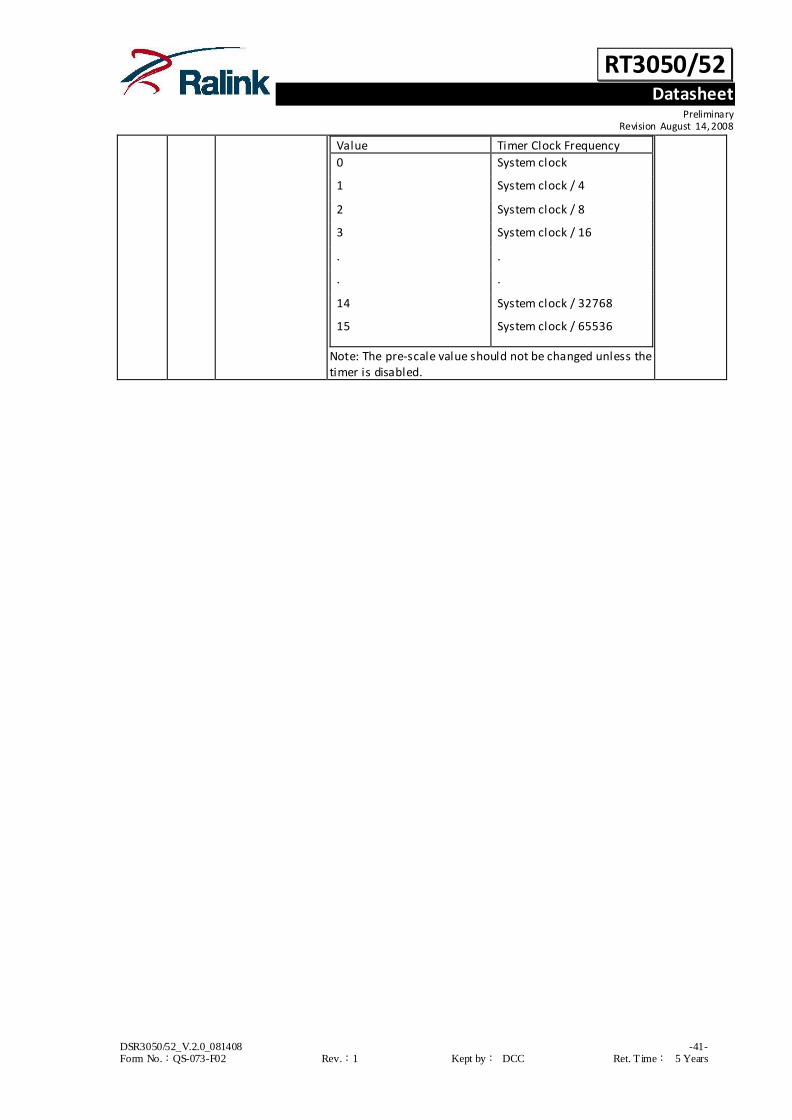
RT3050/52 Datasheet
Preliminary Revision August 14, 2008
DSR3050/52_V.2.0_081408 -41- Form No.:QS-073-F02 Rev.:1 Kept by: DCC Ret. T ime: 5 Years
Value Timer Clock Frequency
0 System clock
1 System clock / 4
2 System clock / 8
3 System clock / 16
. .
. .
14 System clock / 32768
15 System clock / 65536
Note: The pre-scale value should not be changed unless the timer is disabled.

RT3050/52 Datasheet
Preliminary Revision August 14, 2008
DSR3050/52_V.2.0_081408 -42- Form No.:QS-073-F02 Rev.:1 Kept by: DCC Ret. T ime: 5 Years
3.6 Interrupt Controller
3.6.1 Features
Support a central point for interrupt aggregation for platform related blocks
Separated interrupt enable and disable registers
Support global disable function
2-level Interrupt priority selection
Each interrupt source can be directed to IRQ#0 or IRQ#1
Note : RT3052 supports MIPS 24KEc’s vector interrupt mechanism.
There are 6 hardware interrupts supported by MIPS 24KEc. The interrupt allocation is shown below:
MIPS H/W interrupt pins Connect to Remark
HW_INT#5 Timer interrupt Highest priority
HW_INT#4 802.11n NIC
HW_INT#3 Frame Engine
HW_INT#2 Reserved
HW_INT#1 Other high priority interrupts (IRQ#1)
HW_INT#0 Other low priority interrupts (IRQ#0) Lowest priority
3.6.2 Block Diagram
Interrupt MaskingInterrupt
Priority Selection
PalmBus interface
Interrupts
(from platform blocks)
PalmBus
(To/From MIPS)
MIPS 4KEcInterrupt Controller
IRQ0 (low-pri)
IRQ1 (hi-pri)
IRQ from PCI Host/Dev
Frame Engine (Gigabit NIC)
802.11n NIC (Embedded WLAN MAC/BBP)
INT#0
INT#1
INT#4
INT#3
INT#5
MIPS Timer INT
Fig. 3-6-1 Interrupt Controller Block Diagram
3.6.3 Register Description (base: 0x1000.0200)
IRQ0STAT: Interrupt Type 0 Status after Enable Mask (offset: 0x00)
Bits Type Name Description Initial value 31:19 - - Reserved 13’b0
18 RO OTG OTG interrupt status after mask 1’b0
17 RO ESW Ethernet switch interrupt status after mask 1’b0
16 - - Reserved 1’b0
15:13 - - Reserved 3’b0
12 RO UARTLITE UARTLITE interrupt status after mask 1’b0
11 RO - Reserved 1’b0
10 RO I2S I2S interrupt status after mask 1’b0
9 RO PC MIPS performance counter interrupt status after mask 1’b0
8 RO NAND NAND flash controller interrupt status after mask 1’b0

RT3050/52 Datasheet
Preliminary Revision August 14, 2008
DSR3050/52_V.2.0_081408 -43- Form No.:QS-073-F02 Rev.:1 Kept by: DCC Ret. T ime: 5 Years
7 RO DMA DMA interrupt status after mask 1’b0
6 RO PIO PIO interrupt status after mask 1’b0
5 RO UART UART interrupt status after mask
4 RO PCM PCM interrupt status after mask 1’b0
3 RO ILL_ACC Illegal access interrupt status after mask 1’b0
2 RO WDTIMER Watch dog timer interrupt status after mask 1’b0
1 RO TIMER0 Timer 0 interrupt status after mask 1’b0
0 RO SYSCTL System control interrupt status after mask 1’b0
These bits are set if the corresponding interrupt is asserted from the source and with following two conditions
The interrupt is not masked (bit not set in the INTDIS register)
The interrupt type is set to INT0 (in the INTTYPE register).
Note that write to these bits are ignored and each bit cannot be simultaneously active in both the IRQ0STAT and
IRQ1STAT registers.
IRQ1STAT: Interrupt Type 1 Status after Enable Mask (offset: 0x04)
Bits Type Name Description Initial value
31:19 - - Reserved 13’b0
18 RO OTG OTG interrupt status after mask 1’b0
17 RO ESW Ethernet switch interrupt status after mask 1’b0
16 - - Reserved 1’b0
15:13 - - Reserved 3’b0
12 RO UARTLITE UARTLITE interrupt status after mask 1’b0
11 - - Reserved 1’b0
10 RO I2S I2S interrupt status after mask 1’b0 9 RO PC MIPS performance counter interrupt status after mask 1’b0
8 RO NAND NAND flash controller interrupt status after mask 1’b0
7 RO DMA DMA interrupt status after mask 1’b0
6 RO PIO PIO interrupt status after mask 1’b0
5 RO UART UART interrupt status after mask 1’b0
4 RO PCM PCM interrupt status after mask 1’b0
3 RO ILL_ACC Illegal access interrupt status after mask 1’b0
2 RO WDTIMER Watch dog timer interrupt status after mask 1’b0
1 RO TIMER0 Timer 0 interrupt status after mask 1’b0
0 RO SYSCTL System control interrupt status after mask 1’b0
These bits are set if the corresponding interrupt is asserted from the source and with following two conditions
The interrupt is not masked (bit not set in the INTDIS register)
The interrupt type is set to INT1 (in the INTTYPE register).
Note that writing to these bits is ignored and each bit cannot be simultaneously active in both the IRQ0STAT and
IRQ1STAT registers.
INTTYPE: Interrupt Type (offset: 0x20)
Bits Type Name Description Initial value
31:19 - - Reserved 13’b0
18 R/W OTG OTG interrupt status type 1’b0
17 R/W ESW Ethernet switch interrupt status type 1’b0
16 - - Reserved 1’b0
15:13 - - Reserved 3’b0
12 R/W UARTLITE UARTLITE interrupt status type 1’b0
11 - - Reserved 1’b0
10 R/W I2S I2S interrupt status type 1’b0
9 R/W PC MIPS performance counter interrupt status type 1’b0
8 R/W NAND NAND flash controller interrupt status type 1’b0

RT3050/52 Datasheet
Preliminary Revision August 14, 2008
DSR3050/52_V.2.0_081408 -44- Form No.:QS-073-F02 Rev.:1 Kept by: DCC Ret. T ime: 5 Years
7 R/W DMA DMA interrupt status after type 1’b0
6 R/W PIO PIO interrupt status after type 1’b0
5 R/W UART UART interrupt status type 1’b0
4 R/W PCM PCM interrupt status type 1’b0
3 R/W ILL_ACC Illegal access interrupt status type 1’b0
2 R/W WDTIMER Watch dog timer interrupt status type 1’b0
1 R/W TIMER0 Timer 0 interrupt status type 1’b0
0 R/W SYSCTL System control interrupt status type 1’b0
These bits control whether an interrupt is IRQ0 or IRQ1. The interrupt type may be changed at any time; if the
interrupt type is changed while the interrupt is active, the interrupt is immediately redirected.
INTRAW: Raw Interrupt Status before Enable Mask (offset: 0x30)
Bits Type Name Description Initial value
31:19 - - Reserved 13’b0
18 RO OTG OTG interrupt status before mask 1’b0
17 RO ESW Ethernet switch interrupt status before mask 1’b0 16 - - Reserved 1’b0
15:13 - - Reserved 3’b0
12 RO UARTLITE UARTLITE interrupt status before mask 1’b0
11 RO - Reserved 1’b0
10 RO I2S I2S interrupt status before r mask 1’b0
9 RO PC MIPS performance counter interrupt status before mask 1’b0
8 RO NAND NAND flash controller interrupt status before mask 1’b0
7 RO DMA DMA interrupt status before mask 1’b0
6 RO PIO PIO interrupt status before mask 1’b0
5 RO UART UART interrupt status before mask
4 RO PCM PCM interrupt status before mask 1’b0
3 RO ILL_ACC Illegal access interrupt status before mask 1’b0
2 RO WDTIMER Watch dog timer interrupt status before mask 1’b0
1 RO TIMER0 Timer 0 interrupt status before mask 1’b0
0 RO SYSCTL System control interrupt status before mask 1’b0
These bits are set if the corresponding interrupt is asserted from the source. The status bit is set if the interrupt is
active, even if it is masked, and regardless of the interrupt type. This provides a single-access snapshot of all
active interrupts for implementation of a polling system.
INTENA: Interrupt Enable (offset: 0x34)
Bits Type Name Description Initial value
31 R/W GLOBAL
Global interrupt enable
Writing a ‘1’ to this bit allows interrupt masking to be performed based on each interrupt’s individual enable mask. A read returns the global status (‘1’ if enabled).
1’b0
30:19 - - Reserved 12’b0
18 R/W OTG OTG interrupt status after mask 1’b0
17 R/W ESW Ethernet switch interrupt status after mask 1’b0
16 - - Reserved 1’b0
15:13 - - Reserved 3’b0
12 R/W UARTLITE UARTLITE interrupt status after mask 1’b0
11 - - Reserved 1’b0
10 R/W I2S I2S interrupt enable 1’b0
9 R/W PC MIPS performance counter interrupt enable 1’b0
8 RW NAND NAND flash controller interrupt enable 1’b0
7 RW DMA DMA interrupt enable 1’b0
6 RW PIO PIO interrupt enable 1’b0

RT3050/52 Datasheet
Preliminary Revision August 14, 2008
DSR3050/52_V.2.0_081408 -45- Form No.:QS-073-F02 Rev.:1 Kept by: DCC Ret. T ime: 5 Years
5 RW UART UART interrupt enable 1’b0
4 RW PCM PCM interrupt enable 1’b0
3 RW ILL_ACC Illegal access interrupt enable 1’b0
2 RW WDTIMER Watch dog timer interrupt enable 1’b0
1 RW TIMER0 Timer 0 interrupt enable 1’b0
0 RW SYSCTL System control interrupt enable 1’b0
Writing a ‘1’ to these bits (except the GLOBAL bit) will enable the mask for the corresponding interrupt. The
interrupt is asserted and the bit is set in the IRQ0STAT or IRQ1STAT registers if an interrupt is enabled. Writes of
'0' are ignored. Reading either the INTENA or INTDIS register will return the current mask, where an interrupt is
masked (disabled) if the bit is ‘zero’, and unmasked (enabled) if the bit is ‘one’.
INTDIS: Interrupt Disable (offset: 0x38)
Bits Type Name Description Initial value
31 R/W GLOBAL
Global interrupt disable Writing a ‘1’ to this bit allows interrupt masking to be
performed based on each interrupt’s individual Disable mask. A read returns the global status (‘1’ if Disabled).
1’b0
30:19 - - Reserved 12’b0
18 R/W OTG OTG interrupt disable 1’b0
17 R/W ESW Ethernet switch interrupt disable 1’b0
16 - - Reserved 1’b0
15:13 - - Reserved 3’b0
12 R/W UARTLITE UARTLITE interrupt s disable 1’b0
11 - - Reserved 1’b0
10 R/W I2S I2S interrupt disable 1’b0 9 R/W PC MIPS performance counter interrupt disable 1’b0
8 RW NAND NAND flash controller interrupt disable 1’b0
7 RW DMA DMA interrupt disable 1’b0
6 RW PIO PIO interrupt disable 1’b0
5 RW UART UART interrupt disable 1’b0
4 RW PCM PCM interrupt disable 1’b0
3 RW ILL_ACC Illegal access interrupt disable 1’b0
2 RW WDTIMER Watch dog timer interrupt disable 1’b0
1 RW TIMER0 Timer 0 interrupt disable 1’b0
0 RW SYSCTL System control interrupt enable 1’b0
Writing a ‘1’ to these bits (except the GLOBAL bit) will disable the mask for the corresponding interrupt. The
interrupt is asserted and the bit is set in the IRQ0STAT or IRQ1STAT registers if an interrupt is enabled. Writing '0'
is ignored. Reading either the INTENA or INTDIS register will return the current mask, where an interrupt is
masked (disabled) if the bit is ‘zero’, and unmasked (enabled) if the bit is ‘one’.
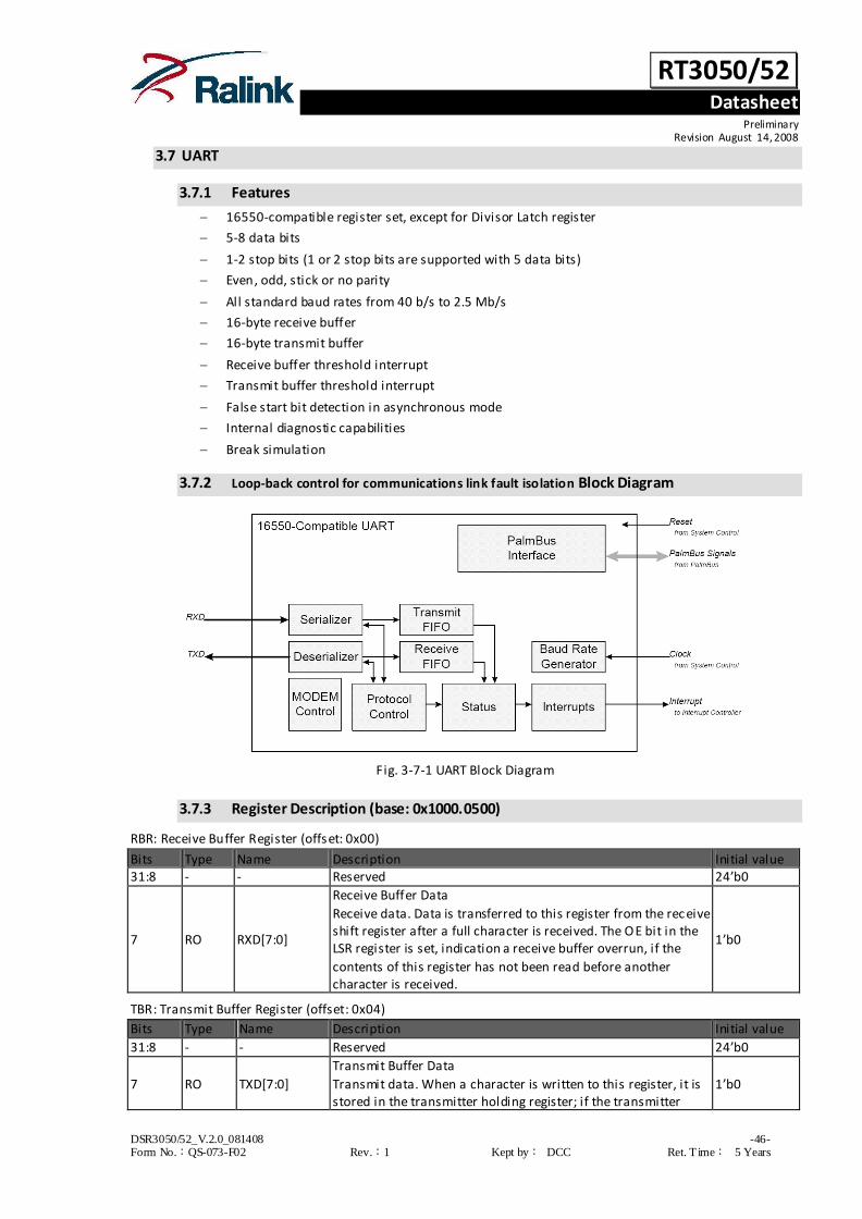
RT3050/52 Datasheet
Preliminary Revision August 14, 2008
DSR3050/52_V.2.0_081408 -46- Form No.:QS-073-F02 Rev.:1 Kept by: DCC Ret. T ime: 5 Years
3.7 UART
3.7.1 Features
16550-compatible register set, except for Divisor Latch register
5-8 data bits
1-2 stop bits (1 or 2 stop bits are supported with 5 data bits)
Even, odd, stick or no parity
All standard baud rates from 40 b/s to 2.5 Mb/s
16-byte receive buffer
16-byte transmit buffer
Receive buffer threshold interrupt
Transmit buffer threshold interrupt
False start bit detection in asynchronous mode
Internal diagnostic capabilities
Break simulation
3.7.2 Loop-back control for communications link fault isolation Block Diagram
Fig. 3-7-1 UART Block Diagram
3.7.3 Register Description (base: 0x1000.0500)
RBR: Receive Buffer Register (offset: 0x00)
Bits Type Name Description Initial value 31:8 - - Reserved 24’b0
7 RO RXD[7:0]
Receive Buffer Data
Receive data. Data is transferred to this register from the rec eive shift register after a full character is received. The OE bit in the LSR register is set, indication a receive buffer overrun, if the
contents of this register has not been read before another character is received.
1’b0
TBR: Transmit Buffer Register (offset: 0x04)
Bits Type Name Description Initial value
31:8 - - Reserved 24’b0
7 RO TXD[7:0]
Transmit Buffer Data
Transmit data. When a character is written to this register, it is stored in the transmitter holding register; if the transmitter
1’b0
RT3050/52 Datasheet
Preliminary Revision August 14, 2008
DSR3050/52_V.2.0_081408 -47- Form No.:QS-073-F02 Rev.:1 Kept by: DCC Ret. T ime: 5 Years
register is empty, the character is moved to the transmitter register, starting transmission.
IER: Interrupt Enable Register (offset: 0x08)
Bits Type Name Description Initial value
31:4 - - Reserved 28’b0
3 R/W EDSSI
Enable Modem Interrupt 1: modem status (DCD, RI, DSR, CTS, DDCD, TERI, DDSR, and
DCTS) interrupts.
0: Disable modem status (DCD, RI, DSR, CTS, DDCD, TERI, DDSR, and DCTS) interrupts.
1’b0
2 R/W ELSI Enable Receiver Line Status Interrupt 1: Enable line status (OE, PE, FE, and BI) interrupts. 0: Disable line status (OE, PE, FE, and BI) interrupts.
1’b0
1 R/W ETBEI
Enable Transmitter Buffer Line Status Interrupt 1: Enable transmit buffer empty (THRE) interrupt. 0: Disable transmit buffer empty (THRE) interrupt.
1’b0
0 R/W ERBFI Enable Receiver Buffer Empty Interrupt 1: Enable data ready (DR) or character time-out interrupt. 0: Disable data ready (DR) or character time-out interrupt.
1’b0
IIR: Interrupt Identification Register (offset: 0x0C)
Bits Type Name Description Initial value
31:8 - - Reserved 24’b0
7:6 RO FIFOENA[1:0]
FIFOs Enabled FIFOs Enabled. These bits reflect the FIFO enable bit setting in
the FIFO Control Register. When the FIFO enable bit is set, both of these bits will be set high to a value of ‘11’. When the FIFO enable bit is cleared, both of these bits will be set low to a value of ’00’.
1’b0
5:4 - - Reserved 2’b0
3:1 RO INTID[2:0]
Interrupt Identifier Interrupt ID. These bits provide a snapshot of the interrupt
type, and may be used as the offset into an interrupt vector table. The interrupt encoding is given below.
ID Priority Type Source
7 6 5 4
3 2 1
0
1 2 3
Undefined Undefined Undefined Undefined
Receiver Line Status Receiver Buffer Full
Transmit buffer Empty Undefined
OE,PE,FE,BI DR THRE
If more than one category of interrupt is asserted, only the highest priority ID will be given. The li ne and Modem status
interrupts are cleared by reading the corresponding status register (LSR, MSR). The Rec eive Buffer Full interrupt will be cleared when all of the data is read from the receiver buffer. The Transmitter Buffer empty will be cleared when data is
written to the TBR register. See also “Interrupt Priorities”.
3’b1

RT3050/52 Datasheet
Preliminary Revision August 14, 2008
DSR3050/52_V.2.0_081408 -48- Form No.:QS-073-F02 Rev.:1 Kept by: DCC Ret. T ime: 5 Years
0 RO INTPEND Interrupt Pending 0: An interrupt bit is set and is not masked.
1: No interrupts are pending.
1’b0
FCR: FIFO Control Register (offset: 0x10)
Bits Type Name Description Initial value
31:8 - - Reserved 24’b0
7:6 R/W RXTRIG[1:0]
Receiver Trigger Level The data ready interrupt (DR) will be asserted when the
receiver buffer depth is equal to the number of characters
programmed in the trigger register. The trigger level
encoding is as follows:
RXTRIG Trigger Level
0 1 2
3
1 4 8
14
Note: This register is not used if the receive FIFO is disabled.
2’b0
5:4 R/W TXTRIG[1:0]
Transmitter Trigger Level The THRE interrupt will be asserted if the transmitter buffer depth is less than or equal to the number of characters programmed in the trigger register. The trigger level encoding is
as follows:
TXTRIG Trigger Level
0 1 2 3
1 4 8 12
2’b0
3 R/W DMAMODE Enable DMA transfers This bit is writeable and readable, but has no other hardware
function.
1’b0
2 W TXRST
Transmitter Reset
Writing a '1' to this bit will clear the transmit FIFO and reset the transmitter status. The shift register is not cleared.
1’b0
1 W RXRST Receive Reset Writing a '1' to this bit will clear the receive FIFO and reset the
receiver status. The shift register is not cleared.
1’b0
0 R/W FIFOENA
0: The Transmit and Receive FIFOs have the effective depth of one character.
1: The Transmit and Receive FIFOs are enabled. Note: The FIFO status and data are automatically cleared when this bit is changed.
1’b0
LCR: Line Control Register (offset: 0x 14, 0x00000000, 0xffffff00, 00)
Bits Type Name Description Initial value
31:8 - - Reserved 24’b0
7 R/W DLAB Divisor Latch Access Bit This bit has no functionality, and is retained for compatibil ity only
2’b0
6 R/W SETBRK
Set Break Condition 0: Normal functionality.
1: Force TXD pin to '0'. Transmitter otherwise operates normally.
2’b0

RT3050/52 Datasheet
Preliminary Revision August 14, 2008
DSR3050/52_V.2.0_081408 -49- Form No.:QS-073-F02 Rev.:1 Kept by: DCC Ret. T ime: 5 Years
5 R/W FORCEPAR
Force Parity Bit 0: Normal functionality.
1: If even parity is selected, the (transmitted and checked) parity is forced to '0'; if odd parity is selected, the (transmitted and checked) parity if forced to '1'.
1’b0
4 R/W EPS
Even Parity Select 0: Odd parity selected (checksum, including parity is '1').
1: Even parity selected (checksum, including parity is '0'). Note: This bit is ignored if the PEN bit is '0'.
1’b0
3 R/W PEN Parity Enable 0: Parity is not transmitted or checked. 1: Parity is generated (transmit), and checked (receive).
1’b0
2 R/W STB
Stop Bit Select
0: 1 stop bit is transmitted and received. 1: 1.5 stop bits are transmitted and received if WLS is '0'; 2 stop bits are transmitted and received if WLS is '1', '2', or '3'.
1’b0
1:0: R/W WLS[1:0]
Word Length Select 0: Each character is 5 bits in length
1: Each character is 6 bits in length 2: Each character is 7 bits in length 3: Each character is 8 bits in length
2’b0
MCR: Modem Control Register (offset: 0x18)
Bits Type Name Description Initial value
31:5 - - Reserved 24’b0
4 R/W LOOP
Loop-back Mode Enable 0: Normal Operation. 1: The UART is put into loop-back mode, used for self-test: The
TXD pin is driven high; the TXD signal connections are made internally
Signal Wrapped back through…
TXD RXD
DTRN DSRN
RTSN CTSN
OUT1N RIN OUT2N DCDN
1’b0
3 R/W OUT2
Out2 Value 0: OUT2N pin is driven to a high level.
1: OUT2N pin is driven to a low level. Note: This bit is only functional in loop-back mode.
0
2 R/W OUT1
Out1 Value 0: OUT1N pin is driven to a high level. 1: OUT1N pin is driven to a low level.
Note: This bit is only functional in loop-back mode.
0
1 R/W RTS Out1 Value 0: RTSN pin is driven to a high level. 1: RTSN pin is driven to a low level.
1’b0
0 R/W DTR Reserved 0: DTRN pin is driven to a high level.
1: DTRN pin is driven to a low level.
1’b0
LSR: Line Status Register (offset: 0x1C)
Bits Type Name Description Initial value
31:8 - - Reserved 24’b0

RT3050/52 Datasheet
Preliminary Revision August 14, 2008
DSR3050/52_V.2.0_081408 -50- Form No.:QS-073-F02 Rev.:1 Kept by: DCC Ret. T ime: 5 Years
7 R/C ERINFIFO The FIFO contains data which had a parity or framing error This bit is set when the FIFO contains data that was received
with a parity error, framing error or break condition.
1’b0
6 R/C TEMT
Transmitter Empty
This bit is set when the transmitter shift register is empty, it will clear as soon as data is written to the TBR register.
1’b0
5 R/C THRE Transmitter Holding Register Empty This bit is set when the transmitter holding register is empty, it
will clear as soon as data is written to the TBR register.
1’b0
4 R/C BI
Break Interrupt
This bit is set if a break is received, that is when the RXD signal is at a low state for more than one character transmission time (from start bit to stop bit). Under this condition, a single 'zero' is
received.
1’b0
3 R/C FE
Framing Error This bit is set if a valid stop bit is not detected. If a framing error occurs, the receiver will attempt to re-synchronize by sampling the Start Bit twice and then takes the data.
1’b0
2 R/C PE
Parity Error
This bit is set if the received parity is different from the expected value.
1’b0
1 R/C OE
Overrun Error This bit is set when a receive overrun occurs. This will happen if a character is received before the previous character has been
read by firmware.
1’b0
0 R/C DR
Data Ready This bit is set when a character is received, and has been transferred in to the rec eiver buffer register. This bit will reset when all the characters are read from the receiver buffer
register.
1’b0
MSR: Modem Status Register (offset: 0x20)
Bits Type Name Description Initial value
31:8 - - Reserved 24’b0
7 R/C DCD Data Carrier Detect This bit is set when the DCDN (Data Carrier Detect) pin is at a
low value.
1’b0
6 R/C RI Ring Indicator This bit is set when the RIN (Ring Indicator) pin is at a low value.
1’b0
5 R/C DSR Data Set Ready This bit is set when the DSRN (Data Set Ready) pin is at a low value.
1’b0
4 R/C CTS
Clear to Send
This bit is set when the CTSN (Clear to Send) pin is at a low value.
1’b0
3 R/C DDCD Delta Data Carrier Detect This bit is set when the DCDN (Data Carrier Detect) pin changes.
1’b0
2 R/C TERI Trailing Edge Ring Indicator This bit is set when the RIN (Ring Indicator) pin changes from a
low to a high value.
1’b0
1 R/C DDSR Delta Data Set Ready This bit is set when the DSRN (Data Set Ready) pin changes.
1’b0
0 R/C DCTS Delta Clear to Send This bit is set when the CTSN (Clear to Send) pin changes.
1’b0
RT3050/52 Datasheet
Preliminary Revision August 14, 2008
DSR3050/52_V.2.0_081408 -51- Form No.:QS-073-F02 Rev.:1 Kept by: DCC Ret. T ime: 5 Years
SCRATCH: Scratch Register (offset: 0x24)
Bits Type Name Description Initial value
31:8 - - Reserved 24’b0
7:0 R/W SCRATCH[7:0]
Scratch This register is defined as a scratch register in 16550 applications. It has no hardware function, and is retained for compatibility only.
8’b0
DL: Clock Divider Divisor Latch (offset: 0x28)
Bits Type Name Description Initial value
31:16 - - Reserved 16’b0
15:0 R/W DL[15:0]
Divisor Latch This register is used in the clock divider to generate the baud
clock. The baud rate (transfer rate in bits per second) is defined as:
Baud rate = system clock frequency / (CLKDIV * 16).
Note: In a standard 16550 implementation, this register is accessible as two 8-bit halves only. In this implementation, the DL register is accessible as a single 16-bit entity only.
16’h0001
DLLO: Clock Divider Divisor Latch Low (offset: 0x2C)
Bits Type Name Description Initial value
31:8 - - Reserved 24’b0
7:0 R/W DLLO[7:0]
This register is the equivalent to the lower 8 bits of the DL register. It is provided for16550 compatibility. Note: In a standard 16550 implementation, this register is
accessible as two 8-bit halves only. For convenience, the divisor latch is accessible as a single 16-bit entity via the DL register.
8’b1
DLHI: Clock Divider Divisor Latch High (offset: 0x30)
Bits Type Name Description Initial value
31:8 - - Reserved 24’b0
7:0 R/W DLHI[7:0]
This register is the equivalent to the upper 8 bits of the DL
register. It is provided for 16550 compatibility. Note: In a standard 16550 implementation, this register is accessible as two 8-bit halves only. For convenience, the divisor
latch is accessible as a single 16-bit entity via the DL register.
8’b0

RT3050/52 Datasheet
Preliminary Revision August 14, 2008
DSR3050/52_V.2.0_081408 -52- Form No.:QS-073-F02 Rev.:1 Kept by: DCC Ret. T ime: 5 Years
3.8 UART Lite
3.8.1 Features
2-pin UART
16550-compatible register set, except for Divisor Latch register
5-8 data bits
1-2 stop bits (1 or 2 stop bits are supported with 5 data bits)
Even, odd, stick or no parity
All standard baud rates from 40 b/s to 2.5 Mb/s
16-byte receive buffer
16-byte transmit buffer
Receive buffer threshold interrupt
Transmit buffer threshold interrupt
False start bit detection in asynchronous mode
Internal diagnostic capabilities
Break simulation
Loop-back control for communications link fault isolation
3.8.2 Block Diagram
Fig. 3-8-1 UART Lite Block Diagram
3.8.3 Register Description (base: 0x1000.0C00)
RBR: Receive Buffer Register (offset: 0x00)
Bits Type Name Description Initial value
31:8 - - Reserved 24’b0
7:0 RO RXD[7:0]
Receive Buffer Data
Receive data. Data is transferred to this register from the receive shift register after a full character is received. The OE bit in the LSR register is set, indication a receive buffer
overrun, if the contents of this register has not been read before another character is received.
8’b0
TBR: Transmit Buffer Register (offset: 0x04)
Bits Type Name Description Initial value 31:8 - - Reserved 24’b0
7:0 RO TXD[7:0]
Transmit Buffer Data
Transmit data. When a character is written to this register, it is stored in the transmitter holding register; if the transmitter register is empty, the character is moved to the transmitter
register, starting transmission.
8’b0

RT3050/52 Datasheet
Preliminary Revision August 14, 2008
DSR3050/52_V.2.0_081408 -53- Form No.:QS-073-F02 Rev.:1 Kept by: DCC Ret. T ime: 5 Years
IER : Interrupt Enable Register (offset: 0x08)
Bits Type Name Description Initial value
31:3 - - Reserved 29’b0
2 R/W ELSI Enable Receiver Line Status Interrupt 1: Enable line status (OE, PE, FE, and BI) interrupts. 0: Disable line status (OE, PE, FE, and BI) interrupts.
1’b0
1 R/W ETBEI Enable Transmitter Buffer Line Status Interrupt 1: Enable transmit buffer empty (THRE) interrupt.
0: Disable transmit buffer empty (THRE) interrupt.
1’b0
0 R/W ERBFI Enable Receiver Buffer Empty Interrupt 1: Enable data ready (DR) or character time-out interrupt. 0: Disable data ready (DR) or character time-out interrupt.
1’b0
IIR: Interrupt Identification Register (offset: 0x0C)
Bits Type Name Description Initial value
31:8 - - Reserved 24’b0
7:6 RO FIFOENA [1 :0]
FIFOs Enabled FIFOs Enabled. These bits reflect the FIFO enable bit setting in the FIFO Control Register. When the FIFO enable bit is set,
both of these bits will be set high to a value of ‘11’. When the FIFO enable bit is cleared, both of these bits will be set low to a value of ’00’.
1’b0
5:4 - - Reserved 2’b0
3:1 RO INTID[2:0]
Interrupt Identifier Interrupt ID. These bits provide a snapshot of the interrupt
type, and may be used as the offset into an interrupt vector table. The interrupt encoding is given below.
ID Priority Type Source
7 6 5
4 3 2
1 0
1 2
3 4
Undefined Undefined Undefined
Undefined Receiver Line Status Receiver Buffer Full
Transmit buffer Empty
Modem Status
OE,PE,FE,BI
DR
THRE DCTD,DDSR, RI,
DCD
If more than one category of interrupt is asserted, only the highest priority ID will be given. The line and Modem status
interrupts are cleared by reading the corresponding status register (LSR, MSR). The Rec eive Buffer Full interrupt will be cleared when all of the data is read from the receiver buffer. The Transmitter Buffer empty will be cleared when data is
written to the TBR register. See also “Interrupt Priorities”.
3’b0
0 RO INTPEND Interrupt Pending 0: An interrupt bit is set and is not masked. 1: No interrupts are pending.
1’b0
FCR: FIFO Control Register (offset: 0x10)
Bits Type Name Description Initial value
31:8 - - Reserved 24’b0
7:6
R/W
RXTRIG [1:0]
Receiver Trigger Level
The data ready interrupt (DR) will be asserted when the receiver buffer depth is equal to the number of characters
2’b0

RT3050/52 Datasheet
Preliminary Revision August 14, 2008
DSR3050/52_V.2.0_081408 -54- Form No.:QS-073-F02 Rev.:1 Kept by: DCC Ret. T ime: 5 Years
programmed in the trigger register. The trigger level encoding is as follows:
RXTRIG Trigger Level
0 1
2 3
1 4
8 14
Note: This register is not used if the receive FIFO is disabled.
5:4 R/W TXTRIG[1:0]
Transmitter Trigger Level The THRE interrupt will be asserted if the transmitter buffer depth is less than or equal to the number of characters
programmed in the trigger register. The trigger level encoding is as follows:
TXTRIG Trigger Level
0 1 2
3
1 4 8
12
2’b0
3 R/W DMAMODE
Enable DMA transfers
This bit is writeable and readable, but has no other hardware function.
1’b0
2 W TXRST Transmitter Reset Writing a '1' to this bit will clear the transmit FIFO and reset the transmitter status. The shift register is not cleared.
1’b0
1 W RXRST
Receive Reset
Writing a '1' to this bit will clear the receive FIFO and reset the receiver status. The shift register is not cleared.
1’b0
0 R/W FIFOENA
0: The Transmit and Receive FIFOs have the effective depth of one character.
1: The Transmit and Receive FIFOs are enabled.
Note: The FIFO status and data are automatically cleared when this bit is changed.
1’b0
LCR: Line Control Register (offset: 0x14)
Bits Type Name Description Initial value
31:8 - - Reserved 24’b0
7 R/W DLAB Divisor Latch Access Bit This bit has no functionality, and is retained for compatibil ity only
2’b0
6 R/W SETBRK
Set Break Condition 0: Normal functionality.
1: Force TXD pin to '0'. Transmitter otherwise operates normally.
2’b0
5 R/W FORCEPAR
Force Parity Bit 0: Normal functionality. 1: If even parity is selected, the (transmitted and checked)
parity is forced to '0'; if odd parity is selected, the (transmitted and checked) parity if forced to '1'.
1’b0
4 R/W EPS
Even Parity Select 0: Odd parity selected (checksum, including parity is '1').
1: Even parity selected (checksum, including parity is '0'). Note: This bit is ignored if the PEN bit is '0'.
1’b0
3 R/W PEN Parity Enable 0: Parity is not transmitted or checked.
1’b0

RT3050/52 Datasheet
Preliminary Revision August 14, 2008
DSR3050/52_V.2.0_081408 -55- Form No.:QS-073-F02 Rev.:1 Kept by: DCC Ret. T ime: 5 Years
1: Parity is generated (transmit), and checked (receive).
2 R/W STB
Stop Bit Select 0: 1 stop bit is transmitted and received. 1: 1.5 stop bits are transmitted and received if WLS is '0'; 2
stop bits are transmitted and received if WLS is '1', '2', or '3'.
1’b0
1:0: R/W WLS[1:0]
Word Length Select 0: Each character is 5 bits in length 1: Each character is 6 bits in length
2: Each character is 7 bits in length 3: Each character is 8 bits in length
2’b0
MCR: Modem Control Register (offset: 0x18)
Bits Type Name Description Initial value
31:5 - - Reserved 24’b0
4 R/W LOOP
Loop-back Mode Enable
0: Normal Operation. 1: The UART is put into loop-back mode, used for self-test: The
TXD pin is driven high; the TXD signal are connected to RXD internally.
1’b0
3:0 RO - Reserved 7’b0
LSR: Line Status Register (offset: 0x1C)
Bits Type Name Description Initial value
31:8 - - Reserved 24’b0
7 R/C ERINFIFO The FIFO contains data which had a parity or framing error This bit is set when the FIFO contains data that was received
with a parity error, framing error or break condition.
2’b0
6 R/C TEMT
Transmitter Empty
This bit is set when the transmitter shift register is empty, it will clear as soon as data is written to the TBR register.
1’b0
5 R/C THRE Transmitter Holding Register Empty This bit is set when the transmitter holding register is empty, it will clear as soon as data is written to the TBR register.
1’b0
4 R/C BI
Break Interrupt
This bit is set if a break is received, that is when the RXD signal is at a low state for more than one character transmission time (from start bit to stop bit). Under this condition, a single
'zero' is received.
1’b0
3 R/C FE
Framing Error
This bit is set if a valid stop bit is not detected. If a framing error occurs, the receiver will attempt to re-synchronize by sampling the Start Bit twice and then takes the data.
1’b0
2 R/C PE
Parity Error
This bit is set if the received parity is different from the expected value.
1’b0
1 R/C OE
Overrun Error This bit is set when a receive overrun occurs. This will happen if a character is received before the previous character has
been read by firmware.
1’b0
0 R/C DR
Data Ready This bit is set when a character is received, and has been transferred in to the rec eiver buffer register. This bit will reset when all the characters are read from the receiver buffer
register.
1’b0

RT3050/52 Datasheet
Preliminary Revision August 14, 2008
DSR3050/52_V.2.0_081408 -56- Form No.:QS-073-F02 Rev.:1 Kept by: DCC Ret. T ime: 5 Years
DL: Clock Divider Divisor Latch (offset: 0x28)
Bits Type Name Description Initial value
31:16 - - Reserved 16’b0
15:0 R/W DL[15:0]
Divisor Latch This register is used in the clock divider to generate the baud clock. The baud rate (transfer rate in bits per second) is defined as:
Baud rate = system clock frequency / (CLKDIV * 16).
Note: In standard 16550 implementation, this register is
accessible as two 8-bit halves only. In this implementation, the DL
register is accessible as a single 16-bit entity only.
16’h0001
DLLO: Clock Divider Divisor Latch Low (offset: 0x2C)
Bits Type Name Description Initial value
31:8 - - Reserved 24’b0
7:0 R/W DLLO[7:0]
This register is the equivalent to the lower 8 bits of the DL register. It is provided for 16550 compatibility. Note: In a standard 16550 implementation, this register is
accessible as two 8-bit halves only. For convenience, the divisor latch is accessible as a single 16-bit entity via the DL register.
8’b1
DLHI:Clock Divider Divisor Latch High (offset: 0x30)
Bits Type Name Description Initial value
31:8 - - Reserved 24’b0
7:0 R/W DLHI[7:0]
This register is the equivalent to the upper 8 bits of the DL register. It
is provided for 16550 compatibility.
Note: In a standard 16550 implementation, this register is
accessible as two 8-bit halves only. For convenience, the divisor latch is accessible as a single 16-bit entity via the DL register.
8’b0
IFCTL:Interface Control (offset: 0x34)
Bits Type Name Description Initial value
31:1 - - Reserved 31’b0
0 R/W IFCTL
Open Collector Mode Control. This register controls if the UART Lite TXD output functions in open collector mode or is
always driven. When set to ‘0’, the output is always driven with the value of the transmit data signal. When set to a ‘1’, the TXD output functions in open collector mode, where the TXD output is either driven low (when the transmit data
output is active low) or tri -stated (when the transmit data output is active high.
1’b0

RT3050/52 Datasheet
Preliminary Revision August 14, 2008
DSR3050/52_V.2.0_081408 -57- Form No.:QS-073-F02 Rev.:1 Kept by: DCC Ret. T ime: 5 Years
3.9 Programmable I/O
3.9.1 Features
Support 52 programmable I/Os
Parameterized numbers of independent inputs, outputs, and inputs
Independent polarity controls for each pin
Independently masked edge detect interrupt on any input transition
Programmable I/O pins are shared pin with SDRAM, PCI, MDIO, JTAG, UART-Lite, UART, SPI, PCM and
I2C.
3.9.2 Block Diagram
Fig. 3-9-1 Program I/O Block Diagram
3.9.3 Register Description (base: 0x1000.0600)
GPIO23_00_INT: Programmed I/O Interrupt Status (offset: 0x00)
Bits Type Name Description Initial value
31:24 - - Reserved 8’b0
23:0 R/C PIOINT[23:0]
A PIOINT bit is set when its corresponding PIO pin changes value
and the edge for that pin is enabled via the PIORMSK or PIOFMSK register. A pin must be set as an input in the PIODIR register to generate an interrupt. All bits are cleared by writing “1” to either this register or the PIOEDGE register.
Note: Changes to the PIO pins can only be detected when the clock is running.
24’b0
GPIO23_00_EDGE: Programmed I/O Edge Status (offset: 0x04)
Bits Type Name Description Initial value
31:24 - - Reserved 8’b0
23:0 R/C PIOEDGE[23:0]
The PIOEDGE bits have different meanings depending on whether the interrupt for that pin is enabled via the PIORMSK or PIOFMSK register. If the interrupt is enabled, upon getting an interrupt condition (the corresponding PIOINT bit will be set), the PIOEDGE
bit will be ‘1’ if a rising edge triggered the interrupt, or ‘0’ if a falling edge triggered the interrupt. If the interrupt is masked (disabled), the PIOEDGE bit will be set on either a rising or falling edge and remain set until cleared by firmware. Bits
corresponding to pins that are not set as inputs will never be set. All bits are cleared by writing “1” to either this register or the
24’b0

RT3050/52 Datasheet
Preliminary Revision August 14, 2008
DSR3050/52_V.2.0_081408 -58- Form No.:QS-073-F02 Rev.:1 Kept by: DCC Ret. T ime: 5 Years
PIOINT register. Note: Changes to the PIO pins can only be detected when the
clock is running.
GPIO23_00_RENA: Programmed I/O Rising Edge Interrupt Enable (offset: 0x08)
Bits Type Name Description Initial value
31:24 - - Reserved 8’b0
23:0 R/W PIORENA[23:0]
Rising edge mask for individual Programmed I/O pin The bits in this register enable the PIO interrupt to be set when
the data on the corresponding PIO pin transitions from a ‘0’ to a ‘1’, i .e. a rising edge. A ‘1’ wi ll allow the interrupt to be set; a ‘0’ will not allow the interrupt so that it will not be set. Note: Edge detection is done after the polarity is adjusted
according to the PIOPOL register.
24’b0
GPIO23_00_FENA: Programmed I/O Falling Edge Interrupt Enable (offset: 0x0C)
Bits Type Name Description Initial value
31:24 - - Reserved 8’b0
23:0 R/W PIOFMASK [23:0]
Falling edge mask for individual Programmed I/O pin
The bits in this register enable the PIO interrupt to be set when the data on the corresponding PIO pin transitions from a ‘1’ to a ‘0’, i .e. a falling edge. A ‘1’ will allow the interrupt to be set; a ‘0’ will not allow the interrupt so that it will not be set.
Note: Edge detection is done after the polarity is adjusted according to the PIOPOL register.
24’b0
GPIO23_00_DATA: Programmed I/O Data (offset: 0x20)
Bits Type Name Description Initial value
31:24 - - Reserved 8’b0
23:0 R/W PIODATA[23:0]
Data Pin for Program I/O These bits are used for driving or sensing static signals on the PIO pins. To drive a value onto a PIO pin, the corresponding bit in the PIODIR register must be set. If the corresponding direction bit is
set, the value written to the bit in the PIODATA register will be driven at the pin. A read of this register returns the value of the signals currently on the PIO pins. Note: The value of any bit in this register will be inverted with
respect to the pin if the corresponding bit in the PIOPOL register is set, both in input and output modes. Note: The values read from the PIO pins are not synchronized;
the user should be sure that the data will not be changing when this register is read, or should be aware that the bits which are not static at that time may be inaccurate.
24’b0
GPIO23_00_DIR: Programmed I/O Direction (offset: 0x24)
Bits Type Name Description Initial value
31:24 - - Reserved 8’b0
23:0 R/W PIODIR[23:0]
Program I/O Pin Direction These bits are used for selecting the data direction of the PIO pins. To configure any pin as an output, the corresponding bit should be set to ‘1’; to configure any pin as an input, the
corresponding bit should be set to ‘0’. The value driven onto the PIO pins, are controlled by the PIOPOL, and PIODATA registers.
24’b0

RT3050/52 Datasheet
Preliminary Revision August 14, 2008
DSR3050/52_V.2.0_081408 -59- Form No.:QS-073-F02 Rev.:1 Kept by: DCC Ret. T ime: 5 Years
GPIO23_00_POL: Programmed I/O Pin Polarity (offset: 0x28)
Bits Type Name Description Initial value
31:24 - - Reserved 8’b0
23:0 R/W PIOPOL[23:0]
Program I/O Pin Polarity These bits are used for controlling the polarity of the data driven
on or read from the PIO pins. To invert the polarity of the data at
any PIO pin, the corresponding bit should be set to ‘1’; a value of
‘0’ will not modify the pin data.
Note: The polarity controls affect both input and output modes.
24’b0
GPIO23_00_SET: Set PIO Data Bit (offset: 0x2C)
Bits Type Name Description Initial value
31:24 - - Reserved 8’b0
23:0 R/C PIOSET[23:0]
These bits are used for setting bits in the PIODATA output register.
Writing a ‘1’ will set the corresponding bit in the PIODATA register. Writing a ‘0’ will have no effect.
24’b0
GPIO23_00_RESET: Clear PIO Data bit (offset: 0x30)
GPIO23_00_TOG: Toggle PIO Data bit (offset: 0x34)
GPIO39_24_INT:Program I/O Interrupt (offset: 0x38)
Bits Type Name Description Initial value
31:16 - - Reserved 16’b0
15:0 R/C PIOINT[15:0]
A PIOINT bit is set when its corresponding PIO pin changes value
and the edge for that pin is enabled via the PIORMSK or PIOFMSK register. A pin must be set as an input in the PIODIR register to generate an interrupt. All bits are cleared by writing “1” to either this register or the PIOEDGE register.
Note: Changes to the PIO pins can only be detected when the clock is running.
16’b0
GPIO39_24_EDGE:Program I/O Edge Status (offset: 0x3c)
Bits Type Name Description Initial value
31:16 - - Reserved 16’b0
15:0 R/C PIOEDGE [15:0]
The PIOEDGE bits have different meanings depending on whether the interrupt for that pin is enabled via the PIORMSK or PIOFMSK register. If the interrupt is enabled, upon getting
an interrupt condition (the corresponding PIOINT bit will be set), the PIOEDGE bit will be ‘1’ if a rising edge triggered the interrupt, or ‘0’ if a falling edge triggered the interrupt. If the interrupt is masked (disabled), the PIOEDGE bit will be set on
either a rising or fall ing edge and remain set until cleared by firmware. Bits corresponding to pins that are not set as inputs
16’b0
Bits Type Name Description Initial value
31:24 - - Reserved 8’b0
23:0 R/C PIORESET[23:0] These bits are used for clearing bits in the PIODATA output register. Writing a ‘1’ will clear the corresponding bit in the PIODATA register. Writing a ‘0’ will have no effect.
24’b0
Bits Type Name Description Initial value
31:24 - - Reserved 8’b0
23:0 R/C PIOTOG[23:0] These bits are used for toggling bits in the PIODATA output register. Writing a ‘1’ will invert the corresponding bit in the PIODATA r egister. Writing a ‘0’ will have no effect.
24’b0

RT3050/52 Datasheet
Preliminary Revision August 14, 2008
DSR3050/52_V.2.0_081408 -60- Form No.:QS-073-F02 Rev.:1 Kept by: DCC Ret. T ime: 5 Years
will never be set. All bits are cleared by writing “1” to either this register or the PIOINT register.
Note: Changes to the PIO pins can only be detected when the clock is running.
GPIO39_24_RENA:Program I/O Rising Edge Interrupt Enable (offset: 0x40)
Bits Type Name Description Initial value
31:16 - - Reserved 16’b0
15:0 R/W PIORENA[15:0]
Rising edge mask for individual Programmed I/O pin The bits in this register enable the PIO interrupt to be set when
the data on the corresponding PIO pin transitions from a ‘0’ to a ‘1’, i .e. a rising edge. A ‘1’ will allow the interrupt to be set; a ‘0’ will not allow the interrupt so that it will not be set. Note: Edge detection is done after polarity is adjusted according
to the PIOPOL register.
16’b0
GPIO39_24_FENA:Program I/O Falling Edge Interrupt Enable(offset: 0x44)
Bits Type Name Description Initial value
31:16 - - Reserved 16’b0
15:0 R/W PIOFENA[15:0]
Falling edge mask for individual Programmed I/O pin The bits in this register enable the PIO interrupt to be set when the data on the corresponding PIO pin transitions from a ‘1’ to a
‘0’, i .e. a falling edge. A ‘1’ will allow the interrupt to be set; a ‘0’ will not allow the interrupt so that it will not be set.
Note: Edge detection is done after polarity is adjusted according to the PIOPOL register.
16’b0
GPIO39_24_DATA:Program I/O Data (offset: 0x48 )
Bits Type Name Description Initial value
31:16 - - Reserved 16’b0
15:0 R/W PIODATA[15:0]
Data Pin for Program I/O These bits are used for driving or sensing static signals on the
PIO pins. To drive a value onto a PIO pin, the corresponding bit in the PIODIR register must be set. If the corresponding direction bit is set, the value written to the bit in the PIODATA register will
be driven at the pin. A read of this register returns the value of the signals currently on the PIO pins. Note: The value of any bit in this register will be inverted with respect to the pin if the corresponding bit in the PIOPOL register
is set, both in input and output modes. Note: The values read from the PIO pins are not synchronized; the user should be sure that the data will not be changing when
this register is read, or should be aware that the bits which are not static at that time may be inaccurate.
16’b0
GPIO39_24_DIR:Program I/O Direction (offset: 0x4c)
Bits Type Name Description Initial value
31:16 - - Reserved 16’b0
15:0 R/W PIODATA[15:0]
Program I/O Pin Direction These bits are used for selecting the data direction of the PIO
pins. To configure any pin as an output, the corresponding bit should be set to ‘1’; to configure any pin as an input, the corresponding bit should be set to ‘0’. The value driven onto the PIO pins, are controlled by the PIOPOL, and PIODATA registers.
16’b0

RT3050/52 Datasheet
Preliminary Revision August 14, 2008
DSR3050/52_V.2.0_081408 -61- Form No.:QS-073-F02 Rev.:1 Kept by: DCC Ret. T ime: 5 Years
GPIO39_24_POL:Program I/O Pin Polarity (offset: 0x50)
Bits Type Name Description Initial value
31:16 - - Reserved 16’b0
15:0 R/W PIOPOL[15:0]
Program I/O Pin Polarity
These bits are used for controlling the polarity of the data driven
on or read from the PIO pins. To invert the polarity of the data
at any PIO pin, the corresponding bit should be set to ‘1’; a
value of ‘0’ will not modify the pin data.
Note: The polarity controls affect both input and output modes.
16’b0
GPIO39_24_SET:Set PIO Data Bit (offset: 0x54)
Bits Type Name Description Initial value
31:16 - - Reserved 16’b0
15:0 R/C PIOSET[15:0] These bits are used for clearing bits in the PIODATA output register. Writing a ‘1’ will clear the corresponding bit in the PIODATA register. Writing a ‘0’ will have no effect.
16’b0
GPIO39_24_RESET:Clear PIO Data bit [39:24](offset: 0x58)
Bits Type Name Description Initial value
31:16 - - Reserved 16’b0
15:0 R/C PIORESET[15:0]
These bits are used for setting bits in the PIODATA output
register. Writing a ‘1’ will set the corresponding bit in the PIODATA register. Writing a ‘0’ will have no effect.
16’b0
GPIO39_24_TOG:Toggle PIO Data bit (offset: 0x5c)
Bits Type Name Description Initial value
31:16 - - Reserved 16’b0
15:0 R/C PIOTOG[15:0] These bits are used for toggling bits in the PIODATA output register. Writing a ‘1’ will invert the corresponding bit in the
PIODATA register. Writing a ‘0’ will have no effect.
16’b0
GPIO51_40_INT:Program I/O Interrupt Status (offset: 0x60)
Bits Type Name Description Initial value
31:12 - - Reserved 20’b0
11:0 R/C PIOINT[11:0]
A PIOINT bit is set when its corresponding PIO pin changes value and the edge for that pin is enabled via the PIORMSK or PIOFMSK register. A pin must be set as an input in the PIODIR register to
generate an interrupt. All bits are cleared by writing “1” to either this register or the PIOEDGE register. Note: Changes to the PIO pins can only be detected when the clock is running.
12’b0
GPIO51_40_EDGE:Program I/O Edge Status (offset: 0x64)
Bits Type Name Description Initial value
23:12 - - Reserved 20’b0
11:0 R/C PIOEDGE[11:0]
The PIOEDGE bits have different meanings depending on whether the interrupt for that pin is enabled via the PIORMSK or PIOFMSK register. If the interrupt is enabled, upon getting an interrupt condition (the corresponding PIOINT bit will be set),
the PIOEDGE bit will be ‘1’ if a rising edge triggered the interrupt, or ‘0’ if a falling edge triggered the interrupt. If the interrupt is masked (disabled), the PIOEDGE bit will be set on
either a rising or fall ing edge and remain set until cleared by firmware. Bits corresponding to pins that are not set as inputs will never be set. All bits are cleared by writing “1” to either this register or the PIOINT register.
12’b0

RT3050/52 Datasheet
Preliminary Revision August 14, 2008
DSR3050/52_V.2.0_081408 -62- Form No.:QS-073-F02 Rev.:1 Kept by: DCC Ret. T ime: 5 Years
Note: Changes to the PIO pins can only be detected when the clock is running.
GPIO51_40_RENA:Program I/O Rising Edge Interrupt Enable (offset: 0x68)
Bits Type Name Description Initial value
23:12 - - Reserved 20’b0
11:0 R/W PIORENA[11:0]
Rising edge mask for individual Programmed I/O pin
The bits in this register enable the PIO interrupt to be set when the data on the corresponding PIO pin transitions from a ‘0’ to a ‘1’, i .e. a rising edge. A ‘1’ will allow the interrupt to be set; a ‘0’
will not allow the interrupt so that it will not be set. Note: Edge detection is done after polarity is adjusted according to the PIOPOL register.
12’b0
GPIO51_40_FENA:Program I/O Falling Edge Interrupt Enable (offset: 0x6C)
Bits Type Name Description Initial value
23:12 - - Reserved 20’b0
11:0 R/W PIORENA[11:0]
Falling edge mask for individual Programmed I/O pin
The bits in this register enable the PIO interrupt to be set when the data on the corresponding PIO pin transitions from a ‘1’ to a ‘0’, i .e. a falling edge. A ‘1’ will allow the interrupt to be set; a ‘0’ will not allow the interrupt so that it will not be set.
Note: Edge detection is done after polarity is adjusted according to the PIOPOL register.
12’b0
GPIO51_40_DATA:Program I/O Data (offset: 0x70 )
Bits Type Name Description Initial value
23:12 - - Reserved 20’b0
11:0 R/W PIODATA[11:0]
Data Pin for Program I/O These bits are used for driving or sensing static signals on the PIO pins. To drive a value onto a PIO pin, the corresponding bit in the PIODIR register must be set. If the corresponding direction
bit is set, the value written to the bit in the PIODATA register will be driven at the pin. A read of this register returns the value of the signals currently on the PIO pins.
Note: The value of any bit in this register will be inverted with respect to the pin if the corresponding bit in the PIOPOL register is set, both in input and output modes. Note: The values read from the PIO pins are not synchronized;
the user should be sure that the data will not be changing when this register is read, or should be aware that the bits which are not static at that time may be inaccurate.
12’b0
GPIO51_40_DIR:Program I/O Direction (offset: 0x74)
Bits Type Name Description Initial value 23:12 - - Reserved 20’b0
11:0 R/W PIODIR [11:0]
Program I/O Pin Direction
These bits are used for selecting the data direction of the PIO pins. To configure any pin as an output, the corresponding bit should be set to ‘1’; to configure any pin as an input, the
corresponding bit should be set to ‘0’. The value driven onto the PIO pins, are controlled by the PIOPOL, and PIODATA registers.
12’b0
GPIO51_40_POL:Program I/O Pin Polarity(offset: 0x78)
Bits Type Name Description Initial value
23:12 - - Reserved 20’b0
RT3050/52 Datasheet
Preliminary Revision August 14, 2008
DSR3050/52_V.2.0_081408 -63- Form No.:QS-073-F02 Rev.:1 Kept by: DCC Ret. T ime: 5 Years
11:0 R/W PIOPOL [11:0]
Program I/O Pin Polarity These bits are used for controlling the polarity of the data driven
on or read from the PIO pins. To invert the polarity of the data at any
PIO pin, the corresponding bit should be set to ‘1’; a value of ‘0’
will not modify the pin data.
Note: The polarity controls affect both input and output modes.
12’b0
GPIO51_40_SET:Set PIO Data Bit (offset: 0x7C)
Bits Type Name Description Initial value
23:12 - - Reserved 20’b0
11:0 R/C PIOSET [11:0]
These bits are used for clearing bits in the PIODATA output
register. Writing a ‘1’ will clear the corresponding bit in the PIODATA register. Writing a ‘0’ will have no effect.
12’b0
GPIO51_40_RESET:Clear PIO Data bit (offset: 0x80)
Bits Type Name Description Initial value
23:12 - - Reserved 20’b0
11:0 R/C PIORESET [11:0] These bits are used for setting bits in the PIODATA output register. Writing a ‘1’ will set the corresponding bit in the
PIODATA register. Writing a ‘0’ will have no effect.
12’b0
GPIO51_40_TOG:Toggle PIO Data bit (offset: 0x84)
Bits Type Name Description Initial value
23:12 - - Reserved 20’b0
11:0 R/C PIOTOG [11:0] These bits are used for toggling bits in the PIODATA output register. Writing a ‘1’ will invert the corresponding bit in the PIODATA register. Writing a ‘0’ will have no effect.
12’b0

RT3050/52 Datasheet
Preliminary Revision August 14, 2008
DSR3050/52_V.2.0_081408 -64- Form No.:QS-073-F02 Rev.:1 Kept by: DCC Ret. T ime: 5 Years
3.10 I2C Controller
3.10.1 Features
Two I2C Host Controllers
Programmable I2C bus clock rate
Supports the Synchronous Inter Integrated Circuits (I2C) serial protocol
Bi-directional data transfer
Programmable address width up to 8 bits
Sequential byte read or write capability
Device address and data address can be transmitted for device, page and address selection
Supports Standard mode and Fast mode
3.10.2 Block Diagram
Fig. 3-10-1 I2C controller Block Diagram
3.10.3 Register Description (base: 0x1000.0900)
CONFIG: I2C Configuration Register (offset: 0x00)
Bits Type Name Description Initial value
31:8 - - Reserved 24’b0
7:5 R/W ADDRLEN [2 :0]
Address Length The value written to this register plus one will indicate the number of address bits to be transferred from the I2C ADDR register. Program ‘0’ for a 1-bit address, ‘1’ for a 2-bit address,
etc.)
3’b0
4:2 R/W DEVADLEN [2:0]
Device Address Length The value written to this register plus one indicates the number of device address bits to be transferred from the DEVADDR register. This field should be programmed to ‘6’ for
compliance with I2C bus protocol.
3’b0

RT3050/52 Datasheet
Preliminary Revision August 14, 2008
DSR3050/52_V.2.0_081408 -65- Form No.:QS-073-F02 Rev.:1 Kept by: DCC Ret. T ime: 5 Years
1 R/W ADDRDIS
0: Normal transfers will occur with the address being Transmitted, followed by read or write data.
1: The controller will read or write serial data without transferring the address.
1’b0
0 R/W DEVADDIS
0: The device address will be transmitted before the data address.
1: The controller will not transfer the device address.
Note: if this bit is set, the ADDRDIS bit is ignored, and an address is always transmitted. Note: most I2C slave devices require a device address to be
transmitted; this bit should typically be set to ‘0’.
1’b0
CLKDIV: I2C Clock Divisor Register (offset: 0x04)
Bits Type Name Description Initial value
31:16 - - Reserved 16’b0
15:0 R/W CLKDIV[15:0]
Clock Divisor The value written to this register is used to generate the I2C
bus SCLK signal by applying the following equation: SCLK frequency = pb_clk frequency / ( 2 x CLKDIV ) Note: pb_clk frequency = 1/3 CPU clock frequency Note: Only values of 8 and above are valid.
Note: Due to synchronization between the I2C internal clock and the system clock, the exact equation is actually SCLK frequency = pb_clk frequency / ((2 x CLKDIV) + 5).
For most systems, CLKDIV is usually programmed to very larger numbers since the system clock frequency should be orders of magnitude faster than the I2C bus clock. These results in the synchronization errors being insignificant and
the exact equation approximating the simpler one given above.
16’b0
DEVADDR: I2C Device Address Register (offset: 0x08)
Bits Type Name Description Initial value
31:7 - - Reserved 25’b0
6:0 R/W DEVADDR[6:0] I2C Device Address This value is transmitted as the device address, if DEVADDIS bit in the CONFIG register is not set to ‘1 ’.
7’b0
ADDR: I2C Address Register (offset: 0x0c)
Bits Type Name Description Initial value
31:8 - - Reserved 24’b0
7:0 R/W ADDR[7:0] I2C Address These bits store the 8-bits of address to be sent to the external I2C slave devices when the ADDRDIS bit is ‘0’.
8’b0
DATAOUT: I2C Data Out Register (offset: 0x10)
Bits Type Name Description Initial value
31:8 - - Reserved 24’b0
7:0 R/W DATAOUT [7:0] I2C Data Out These bits store the 8-bits of data to be written to the external I2C slave devices during a write transfer.
8’b0
DATAIN: I2C Data In Register (offset: 0x14)
Bits Type Name Description Initial value
31:8 - - Reserved 24’b0
RT3050/52 Datasheet
Preliminary Revision August 14, 2008
DSR3050/52_V.2.0_081408 -66- Form No.:QS-073-F02 Rev.:1 Kept by: DCC Ret. T ime: 5 Years
7:0 RO DATAIN[7:0]
I2C Data In These bits store the 8-bits of data received from the external
I2C slave devices during a read transaction. The DATARDY bit in the STATUS register is set to ‘1’ when data is valid in this register.
8’b0
STATUS: I2C Status Register (offset: 0x18)
Bits Type Name Description Initial value
31:5 - - Reserved 27’b0
4 RO STARTERR
Start Overflow Error This bit is set when the STARTXFR register is written and a transfer is in progress. When this occurs, the write to the
STARTXFR register is ignored. This bit is automatically cleared if firmware writes to the STARTXFR register when the BUSY bit cleared.
1’b0
3 RO ACKERR
I2C Acknowledge Error Detect This bit is set when the Host controller di d not receive a proper
acknowledge from the I2C slave device after the transmission of a device address, address, or data out. This bit is automatically cleared when firmware writes to the STARTXFR
register.
1’b0
2 RO DATARDY
I2C Data Ready for Read This bit indicates that the receive buffer contains valid data. It is set when data is received from an I2C slave device and is transferred from the interface shift register to the DATAIN
register. This bit is automatically cleared when firmware reads the DATAIN register.
1’b0
1 RO SDOEMPTY
I2C Serial Data Out Register Empty This bit indicates that the transmit data buffer is empty. It is cleared when the DATAOUT register is written to by software, and set to ‘1’ when transmit data is transferred from the
DATAOUT register to the interface shift register. Firmware may write to the DATAOUT register when this bit is ‘1’.
1’b1
0 RO BUSY
I2C State Machine Busy This bit is ‘1’ when the I2C interface is active, and ‘0’ when it is idle. Firmware may initiate an I2C transfer when this bit is ‘0’,
and should not modify any I2C host controller registers while it is ‘1’.
1’b0
STARTXFR: I2C Transfer Start Register (offset: 0x1C)
Bits Type Name Description Initial value
31:2 - - Reserved 30’b0
1 R/W NODATA
Initiate transfer without transferring data When this register is written with this bit set, an address -only transaction is initiated. If DEVADDIS is ‘0’, the device address,
direction, address and stop condition are transmitted to the I2C slave device. If DEVADDIS is ‘1’, the address and stop condition are transmitted to the I2C slave device. This bit should be written with a ‘0’ for normal I2C bus accesses.
Note: ADDRDIS is ignored if this bit is set for a transaction.
1’b0
0 R/W RWDIR
Read/Write Direction When this register is written with this bit set, a read transaction is initiated; when written with this bit reset, a write transaction
is initiated. Note: this bit is shifted out to the I2C slave device after the
1’b0

RT3050/52 Datasheet
Preliminary Revision August 14, 2008
DSR3050/52_V.2.0_081408 -67- Form No.:QS-073-F02 Rev.:1 Kept by: DCC Ret. T ime: 5 Years
device address; if DEVADDIS is ‘1’, this bit is not shifted out to the device.
BYTECNT: I2C Byte Counter Register (offset: 0x20)
Bits Type Name Description Initial value
31:6 - - Reserved 26’b0
5:0 R/W BYTCNT[5:0]
Byte Count used for sequential reads/writes The value written to this register plus one indicates the
number of data bytes to be written to or read from the external I2C slave device. If its value is non-zero, multiple sequential read or write cycles will be issued with a single address (and/or device address).
6’b0

RT3050/52 Datasheet
Preliminary Revision August 14, 2008
DSR3050/52_V.2.0_081408 -68- Form No.:QS-073-F02 Rev.:1 Kept by: DCC Ret. T ime: 5 Years
3.11 SPI Controller
3.11.1 Features
Supports SPI master operations
Programmable clock polarity
Programmable interface clock rate
Programmable bit ordering
Firmware-controlled SPI enable
Programmable payload (address + data) length
3.11.2 Block Diagram
Fig. 3-11-1 SPI control ler Block Diagram
3.11.3 Register Description (base: 0x1000.0B00)
SPISTAT: SPI Interface Status (offset: 0x00)
Bits Type Name Description Initial value
31:2 - - Reserved 30’b0
0 RO BUSY
SPI transfer in progress 0: The SPI interface is inactive.
1: An SPI transfer is in progress.
Note: This bit must be ‘0’ before initiating a transfer. Any
attempt to start a data transfer will be ignored if this bit is a ‘1’.
1’b0
SPICFG: SPI Interface Configuration (offset: 0x10)
Bits Type Name Description Initial value
31:9 - - Reserved 23’b0
8 R/W MSBFIRST
Bit transfer order
0: LSB bits of data sent/received first. 1: MSB bits of data sent/received first. Note: This bit applies to both the command and data.
1’b1
7 - - Reserved 1’b0
6 R/W SPICLKPOL
SPI clock default state 0: The default state of the SPICLK is logic ‘0’. 1: The default state of the SPICLK is logic ‘1’. Note: This bit is ignored if the SPI interface block is a slave
(SPISLAVE bit is set).
1’b0
5 R/W RXCKEDGE SPI clock default state 0: Data is captured on the rising edge of the SPICLK signal. 1: Data is captured on the falling edge of the SPICLK signal.
1’b0

RT3050/52 Datasheet
Preliminary Revision August 14, 2008
DSR3050/52_V.2.0_081408 -69- Form No.:QS-073-F02 Rev.:1 Kept by: DCC Ret. T ime: 5 Years
4 R/W TXCKEDGE SPI clock default state 0: Data is transmitted on the rising edge of the SPICLK signal.
1: Data is transmitted on the falling edge of the SPICLK signal.
1’b0
3 R/W HIZSPI
Tri-state all SPI pin 0: SPICLK and SPIENA pin are driven. 1: SPICLK and SPIENA pin are tri -stated.
Note: This bit overrides all normal functionality.
1’b0
2:0 R/W SPICLK[2:0]
SPI clock divide control (the rate in following table should be change in the future)
0: SPICLK rate is system clock rate/ 2 1: SPICLK rate is system clock rate / 4 2: SPICLK rate is system clock rate / 8 3: SPICLK rate is system clock rate / 16
4: SPICLK rate is system clock rate / 32 5: SPICLK rate is system clock rate / 64 6: SPICLK rate is system clock rate / 128 7: SPICLK is disabled
3’b0
SPICTL: SPI Interface Control (offset: 0x14)
Bits Type Name Description Initial value
31:4 - - Reserved 28’b0
3 R/W HIZSDO
Tri-state data out 0: The SPIDO pin remains driven after the cycle is complete. 1: The SPIDO pin is tri -stated after the cycle is complete.
Note: This bit applies to write transfers only; for read transfers the SPIDO pin is tri -stated during the transfer.
1’b0
2 W STARTWR
Start SPI write transfer When this bit is written with a ‘1’, the contents of the SPIDATA register are transferred to the SPI slave device. Writing a ’0’ to
this register has no effect. Note: The BUSY bit in the SPISTAT register is set when this bit is set and is cleared when the data transfer is complete. This bit is
only meaningful if the SPI interface block is configured as a master.
1’b0
1 W STARTRD
When this bit is written with a ‘1’, a read from the SPI slave is
started; the read data is placed in the SPIDATA regi ster. Writing
a ’0’ to this register has no effect.
Note: The BUSY bit in the SPISTAT register is set when a this bit is
set and is cleared when the data transfer is complete. This bit is
only meaningful if the SPI interface block is configured as a
master.
1’b0
0 R/W SPIENA 0: The SPIENA pin is negated. 1: The SPIENA pin is asserted.
1’b0
SPIDATA: SPI Interface Data (offset: 0x20)
Bits Type Name Description Initial value
31:8 - - Reserved 24’b0
7:0 R/W SPIDATA[7:0]
This register is used for command/data transfers on the SPI interface. The use of this register is given below: Write: the bits to be transferred are written here, including both
command and data bits. If values are transmitted MSB (most
significant bit) first, the command is placed in the upper bits and
the data in the lower bits. Bit 0 of the data is written to SPIDATA
8’b0

RT3050/52 Datasheet
Preliminary Revision August 14, 2008
DSR3050/52_V.2.0_081408 -70- Form No.:QS-073-F02 Rev.:1 Kept by: DCC Ret. T ime: 5 Years
[0];bit 0 of the command follows the MSB of the data. If data is
transmitted LSB (least significant bit) first, the command is placed
in the lower bits and the data is placed in the upper bits.
Read: the command bits are written here. Bit 0 of the command is written to SPIDATA[0]. When the transfer is complete, the data
transferred from the slave may be read from the lower bits of this register.

RT3050/52 Datasheet
Preliminary Revision August 14, 2008
DSR3050/52_V.2.0_081408 -71- Form No.:QS-073-F02 Rev.:1 Kept by: DCC Ret. T ime: 5 Years
3.12 Generic DMA Controller
3.12.1 Features
Support 8 DMA channels
Support 8 DMA requests
Programmable hardware channel priority
Programmable DMA Burst Size (1,2,4,8,16 burst transfer)
Support 32 bit wide transaction
Big-endian and Little-endian support
Support memory to memory, memory to peripheral, peripheral to memory, peripheral to
peripheral transfers.
Interrupts for each channel. They also can be masked, independently.
Each channel transaction can be masked temporarily by the software, and rel eased by the
hardware automatically.
3.12.2 Block Diagram
DMA Engine
RbusMaster
RbusMaster
Arbiter
Pbus Slave
Ch0
Ch7
Mux
InterruptController
Rbus Interface (Master)
Pbus Interface (Slave)
Rbus Interface(Master)
DMA Interface
Interrupt Interface
Fig. 3-12-1 Generic DMA controller Block Diagram
3.12.3 Register Description (base: 0x10000700)
GDMASAn: GDMA Channel n Source Address (offset: 0x00, 0x10, 0x20, 0x3 0, 0x40, 0x50, 0x60, 0x70 ) (n:0~7)
Bits Type Name Description Initial value
31:0 R/W CHANNEL SOURCE ADDRESS
Channel Source Address: This register contains the source address information
32’b0
GDMADAn: GDMA Channel n Destination Address (offset: 0x04, 0x14, 0x24, 0x34, 0x44, 0x54, 0x64, 0x74 ) (n:0~7)
Bits Type Name Description Initial value
31:0 R/W
CHANNEL
DESTINATION ADDRESS
Channel Destination Address:
This register contains the destination address information 32’b0

RT3050/52 Datasheet
Preliminary Revision August 14, 2008
DSR3050/52_V.2.0_081408 -72- Form No.:QS-073-F02 Rev.:1 Kept by: DCC Ret. T ime: 5 Years
GDMACT0n: GDMA Channel n Control Register 0 (offset: 0x08, 0x18, 0x28, 0x38, 0x48, 0x58, 0x68, 0x78)
Bits Type Name Description Initial value
31:16 R/W Transfer Count These registers contain the number of the data bytes needed to be transfer.
12’b0
15:12 R/W
Source
DMA
Request
The value represents the source DMA request.
‘b0000: DMA_REQ0 ‘b0001: DMA_REQ1 (NAND-flash) ‘b0010: DMA_REQ2 (I2S)
‘b0011: DMA_REQ3 (PCM0-RX) ‘b0100: DMA_REQ4 (PCM1-RX) ‘b0101: DMA_REQ5 (PCM0-TX) ‘b0110: DMA_REQ6 (PCM1-TX)
‘b0111: DMA_REQ7 ‘b1000: The source of the transfer is memory
4’b0
11:8 R/W Destination
DMA Request
The value represents the destination DMA request. ‘b0000: DMA_REQ0 ‘b0001: DMA_REQ1 (NAND-flash) ‘b0010: DMA_REQ2 (I2S)
‘b0011: DMA_REQ3 (PCM0-RX) ‘b0100: DMA_REQ4 (PCM1-RX) ‘b0101: DMA_REQ5 (PCM0-TX)
‘b0110: DMA_REQ6 (PCM1-TX) ‘b0111: DMA_REQ7 ‘b1000: The destination of the transfer is memory
4’b0
7 R/W Source Burst
Mode
The value represents the source burst mode
‘b0: incremental mode ‘b1: fix mode
1’b0
6 R/W Destination Burst Mode
The value represents the destination burst mode ‘b0: incremental mode ‘b1: fix mode
1’b0
5:3 R/W Burst Size
The number of the transfer for burst transaction.
‘b000: 1 transfer ‘b001: 2 transfer ‘b010: 4 transfer
‘b011: 8 transfer ‘b100: 16 transfer others: undefined
3’b0
2 R/W Transmit Done
Interrupt Enable
Transmit done interrupt enable. ‘b1:Enable
‘b0:Disable
1’b0
1 R/W Channel Enable
Enable the channel ‘b1: Enable ‘b0: Disable
This bit will be de-asserted by the hardware when the transaction is done.
1’b0
0 R/W Hardware/Software Mode Select
Hardware/Software Mode Select ‘b1: Software Mode
‘b0: Hardware Mode In software mode, the data transfer will start when the Channel Enable bit is set. In hardware mode, the data transfer will start when the DMA
Request is asserted.
1’b0

RT3050/52 Datasheet
Preliminary Revision August 14, 2008
DSR3050/52_V.2.0_081408 -73- Form No.:QS-073-F02 Rev.:1 Kept by: DCC Ret. T ime: 5 Years
GDMACT1n: GDMA Channel n Control Register 1 (offset: 0x0C, 0x1C, 0x2C, 0x3C, 0x4C, 0x5C, 0x6C, 0x7C)
Bits Type Name Description Initial value
31:5 -- - Reserved --
4 R/W
Channel Unmasked
Interrupt Enable
Channel unmasked interrupt enabl e. ‘b1:Enable ‘b0:Disable When this bit is set, an interrupt will be asserted when the
hardware wants to clear the Channel Mask bit and the Channel Mask bit is 0 originally.
1’b0
3:1 R/W Next Unmasked
Channel
The value represents the next unmasked channel . When the transaction is done, the hardware will clear the Channel Mask bit of the next unmasked channel.
‘b000: Channel 0 ‘b001: Channel 1 ‘b010: Channel 2 ‘b011: Channel 3
‘b100: Channel 4 ‘b101: Channel 5 ‘b110: Channel 6
‘b111: Channel 7
If the hardware doesn’t need to clear any Channel Mask bit,
these bits must be set to their own channel.
4’b0
0 R/W Channel Mask
Channel Mask
‘b1: This channel is masked ‘b0: This channel is not masked When this channel mask is set, the GDMA transaction will not start until this bit is clear by the hardware.
1’b0
GDMAISTS: GDMA Interrupt Status Register (offset: 0x80)
Bits Type Name Description Initial value
31:24 - - Reserved -
23:16 R/W1C Unmasked Interrupt Status
This register contains the unmasked interrupt status. This bit will be set when the hardware wants to clear the Channel Mask bit and the Channel Mask bit is 0 originally.
Bit23~bit16 is for channel 7 ~ channel 0, respectively.
8’b0
15:8 - - Reserved -
7:0 R/W1C Transmit Done Interrupt Status
This register contains the transmit-done interrupt status. Bit7~bit0 is for channel 7 ~ channel 0, respectively.
8’b0
GDMASSTS: GDMA Signal Status Register (offset: 0x84)
Bits Type Name Description Initial value
31:24 - - Reserved -
23:16 R GDMA Request Signal Status
This register contains the GDMA Request Signals status Bit7~bit0 is for GDMA_REQ7 ~ GDMA_REQ0, respectively.
8’b0
15:8 R GDMA ACK
Signal Status
This register contains the GDMA ACK signals status
Bit7~bit0 is for GDMA_ACK7 ~ GDMA_ACK0, respectively. 8’b0
7:0 R GDMA Finish
Signal Status
This register contains the GDMA Finish signals status
Bit7~bit0 is for GDMA_Finish7 ~ GDMA_Finish0, respectively. 8’b0
GDMAGCT: GDMA Global Control Register (offset: 0x88)
Bits Type Name Description Initial value
31:1 - - Reserved -

RT3050/52 Datasheet
Preliminary Revision August 14, 2008
DSR3050/52_V.2.0_081408 -74- Form No.:QS-073-F02 Rev.:1 Kept by: DCC Ret. T ime: 5 Years
0 R/W Arbitration Selection
Select the channel arbitration method. 1’b0: Channel 0 has the highest priority. Channel 1~ Channel7 are
round-robin. 1’b1: Channel 0 doesn’t have the highest priority.
Channel0~Channel7 are round-robin.
1’b0

RT3050/52 Datasheet
Preliminary Revision August 14, 2008
DSR3050/52_V.2.0_081408 -75- Form No.:QS-073-F02 Rev.:1 Kept by: DCC Ret. T ime: 5 Years
3.13 PCM Controller
3.13.1 Features
PCM module provides PBUS interface for register configuration and data transfer
Two clock sources are reserved for PCM circuit. (From internal clock generator, int_pcm_clk,
and from external clock source, ext_pcm_clk)
PCM module can drive a clock out to external codec (out_clk_freq = int_pcm_clk/n, n =
configurable by register, 1<=n<=64).
2 channels PCM are available. 4~128 slots are configurable.
Each channel supports a-law(8-bits)/u-law(8-bits)/raw-PCM(16-bits) transfer.
Hardware converter of a-lawraw-16 and u-law raw-16 are implemented in design.
Support long/short FSYNC.
All signals are driven by rising edge and latched by fall ing edge.
Last bit of DTX will be tri-stated on falling edge.
Begin of slot is configurable by 10 bits registers each channel.
32 bytes FIFO are available for each channel
3.13.2 Block Diagram
Fig. 3-13-1 PCM Controller Block Diagram
Two clocks domains are partitioned in this design. PCM converter (ulawraw-16bit and alawraw-16bit) are
implemented in PCM mxDmx. The threshold of FIFO is configurable.
As the threshold reachs, PCM will (a) trigger the DMA interface to notify external DMA engine to transfer data.
(b) trigger the interrupts to host.
The interrupt sources include :
- threshold is reached
- FIFO under run or overrun.
- fault is detected at DMA interface.
Pbus Itf
RFIFO (32 bytes)
TFIFO (32 bytes)
RFIFO (32 bytes)
TFIFO (32 bytes)
CH1
PCM csr
PBUS
PCM IF
SYS clock domain PCM clock domain
PCM module
GDMA Itf CH0
a/ulaw a/ulaw
RT3050/52 Datasheet
Preliminary Revision August 14, 2008
DSR3050/52_V.2.0_081408 -76- Form No.:QS-073-F02 Rev.:1 Kept by: DCC Ret. T ime: 5 Years
The A-law and u-law converter is implemented base on ITU-G.711 A-law and u-law table. In this design, support
a-law/u-law(8-bits) linear PCM(16-bits) only. A-law u-law isn’t available now.
The data-flow from codec to PCM-controller (RX-flow) is shown as below: PCM-controller latches the data from DRX at indicated time slot and then writes it to FIFO. If FIFO full, the d ata
will be lost.
As the RX-FIFO reach the threshold, two actions may be taken
As DMA_ENA=1, DMA_REQ will be asserted to request a burst transfer. And it will re-check the FIFO threshold
after DMA_END is asserted by GDMA. (GDMA should be configured before channel is enabled.)
Assert the Interrupt source to notify HOST. HOST can check RFIFO_AVAIL information then get back the data from
FIFO.
The data-flow from PCM-controller to codec (TX-flow) is shown as below:
After GDMA is configured, software should configure and enable the PCM channel.
The empty FIFO should
As DMA_ENA=1, DMA_REQ will be triggered to request a burst transfer. And it will re-check the FIFO threshold
after DMA_END is asserted by GDMA (a burst is completed.).
Assert the Interrupt source to notify HOST. HOST will write down the data to TX-FIFO. After that, HOST will
recheck TFIFO_EMPTY information then write more data if available.
NOTICE: As DMA_ENA=1, the burst size of GDMA should less than the threshold value.
3.13.3 Register Description (base: 0x1000.0400)
GLB_CFG: GLB_CFG Register (offset: 0x00)
Bits Type Name Description Initial value
31 RW PCM_EN PCM enable, 1: enable 0: disable, all FSM and control register of PCM_mxDmx will be
clear to default value.
0
30 RW DMA_EN DMA enable
1: enable DMA interface, transfer data with DMA 0: disable DMA interface, transfer data with software.
0
29:23 - - Reserved 0
22:20 RW RFF_THRES RXFIFO threshold, As threshold reach, host/dma will be notified to fi ll FIFO. (unit = word) It should be >2 and <6
As data in FIFO under the threshold, interrupt & DMA will be triggered.
4
19 - - Reserved 0
18:16 RW TFF_THRES TXFIFO threshold, As threshold reach, host/dma will be notified to fi ll FIFO. (unit = word) It should be >2 and <6.
As data in FIFO over the threshold, interrupt & DMA will be triggered.
4
15:10 - - Reserved 0
9 RW CH1-TX_EN Channel-1 TX enable 0
8 RW CH0-TX_EN Channel-0 TX enable 0
7:2 - - Reserved 0
1 RW CH1-RX_EN Channel-1 RX enable 0
0 RW CH0-RX_EN Channel-0 RX enable 1: enable 0:disable
0

RT3050/52 Datasheet
Preliminary Revision August 14, 2008
DSR3050/52_V.2.0_081408 -77- Form No.:QS-073-F02 Rev.:1 Kept by: DCC Ret. T ime: 5 Years
PCM_CFG: PCM_CFG Register (offset: 0x04)
Bits Type Name Description Initial value
31 RW EXT_CLK_EN PCM_CLK is generated by external source. 1: PCM_CLK is provided by external
0: PCM_CLK is generated by internal clock divider
0
30 RW CLKOUT_EN
Enable the PCM_CLK_OUT 1: PCM_CLK_OUT should be free run 0: PCM_CLK_OUT should be pull -low forever.
(NOTE: Normally, the register should be asserted to ‘1’. And it should be asserted after divider cfg & divider clock enable)
0
29:28 - - Reserved
27 RW EXT_FSYNC FSYNC is provided by external. 1: FSYNC is provided by external 0: FSYNC is generated by internal circuit.
0
26 RW LONG_FSYNC
FSYNC mode:
1: long FSYNC 0: short FSYNC
0
25 RW FSYNC_POL Polarity of FSYNC 1: FSYNC is high active 0: FSYNC is low active
1
24 RW DRX_TRI
Tristate the DRX as fall edge as LSB bit.
1: Tristate the DRX 0: non- Tristate the DRX
1
23:3 - - Reserved 0
2:0 RW SLOT_MODE
How many slot each PCM frame 0: 4 slots, PCM clock out/in should be 256KHz.
1: 8 slots, PCM clock out/in should be 512KHz. 2:16 slots, PCM clock out/in should be 1.024MHz. 3:32 slots, PCM clock out/in should be 2.048MHz. 4:64 slots, PCM clock out/in should be 4.096MHz.
5:128 slots, PCM clock out/in should be 8.192MHz. other: reserved. Note: When using the external cl ock, the frequency clock should
be equal to PCM_clock out. Otherwise, the PCM_CLKin should be 8.192 MHz.
0
INT_STATUS: INT_STATUS Register (offset: 0x08)
Bits Type Name Description Initial value
31:16 RO - Reserved 0
15 RW CH1T_DMA_ FAULT
Found any fault of the CH1-TX’s DMA signals. (Write ‘1’ to clear) 0
14 RW CH1T_OVRUN The FIFO of CH1-TX overrun(Write ‘1’ to clear)
13 RW CH1T_UNRUN The FIFO of CH1-TX underrun(Write ‘1’ to clear) 0
12 RW CH1T_THRES The FIFO of CH1-TX lower than the defined threshol d. (Write ‘1’
to clear)
0
11 RW CH1R_DMA_ FAULT
Found any fault of the CH1-RX’s DMA signals. (Write ‘1’ to clear) 0
10 RW CH1R_OVRUN The FIFO of CH1-RX overrun(Write ‘1’ to clear)
9 RW CH1R_UNRUN The FIFO of CH1-RX underrun(Write ‘1’ to clear) 0
8 RW CH1R_THRES The FIFO of CH1-RX lower than the defined threshold. (Write ‘1’ to clear)
0
7 RW CH0T_DMA_ FAULT
Found any fault of the CH0-TX’s DMA signals. (Write ‘1’ to clear) 0
6 RW CH0T_OVRUN The FIFO of CH0-TX overrun(Write ‘1’ to clear)

RT3050/52 Datasheet
Preliminary Revision August 14, 2008
DSR3050/52_V.2.0_081408 -78- Form No.:QS-073-F02 Rev.:1 Kept by: DCC Ret. T ime: 5 Years
5 RW CH0T_UNRUN The FIFO of CH0-TX underrun(Write ‘1’ to clear) 0
4 RW CH0T_THRES The FIFO of CH0-TX lower than the defined threshold. (Write ‘1’ to clear)
0
3 RW CH0R_DMA_FAULT
Found any fault of the CH0-RX’s DMA signals. (Write ‘1’ to clear) 0
2 RW CH0R_OVRUN The FIFO of CH0-RX overrun(Write ‘1’ to clear)
1 RW CH0R_UNRUN The FIFO of CH0-RX underrun(Write ‘1’ to clear) 0
0 RW CH0R_THRES The FIFO of CH0-RX lower than the defined threshold. (Write ‘1’
to clear)
0
INT_EN: INT_EN Register (offset: 0x0c)
Bits Type Name Description Initial value
31:16 RO - Reserved 0
15 RW INT15_EN Enable INT_STATUS[15] 0
14 RW INT14_EN Enable INT_STATUS[14] 0
13 RW INT13_EN Enable INT_STATUS[13] 0
12 RW INT12_EN Enable INT_STATUS[12] 0
11 RW INT11_EN Enable INT_STATUS[11] 0
10 RW INT10_EN Enable INT_STATUS[10] 0
9 RW INT9_EN Enable INT_STATUS[9] 0
8 RW INT8_EN Enable INT_STATUS[8] 0
7 RW INT7_EN Enable INT_STATUS[7] 0
6 RW INT6_EN Enable INT_STATUS[6] 0
5 RW INT5_EN Enable INT_STATUS[5] 0
4 RW INT4_EN Enable INT_STATUS[4] 0
3 RW INT3_EN Enable INT_STATUS[3] 0
2 RW INT2_EN Enable INT_STATUS[2] 0
1 RW INT1_EN Enable INT_STATUS[1] 0
0 RW INT0_EN Enable INT_STATUS[0] 0
FF_STATUS: FF_STATUS Register (offset: 0x10)
Bits Type Name Description Initial value
31:16 - - Reserved 0
15:12 RO CH1RFF_AVCNT CH1, Available FIFO space can be read (unit=word) 0
11:8 RO CH1TFF_EPCNT CH1, Available FIFO space can be written (unit=word) 8
7:4 RO CH0RFF_AVCNT CH0, Available FIFO space can be read (unit=word) 0
3:0 RO CH0TFF_EPCNT CH0, Available FIFO space can be written (unit=word) 8
CH0_CFG: CH0_CFG Register (offset: 0x020)
Bits Type Name Description Initial value
31 RW LBK_EN Loopback enable
1: loopback (Asyn-TXFIFODTXDRXAsyn-RXFIFO) 0: normal mode
0
30 RW EXT_LBK_EN External loopback enable 1: external loopback enable
(Ext-CodecDRXDTXExt-Codec) 0: normal mode
0
29:28 RW CMP_MODE Compress type select 0: disable HW converter, l inear raw-data (16-bits)
1: disable HW converter, A-law or U-law (8-bits) 2: enable HW converter, raw-data(16-bits) U-law mode (8-
bits) 3: enable HW converter, raw-data(16-bits) A-law mode (8-
bits)
0
RT3050/52 Datasheet
Preliminary Revision August 14, 2008
DSR3050/52_V.2.0_081408 -79- Form No.:QS-073-F02 Rev.:1 Kept by: DCC Ret. T ime: 5 Years
27:10 - - Reserved 0
9:0 RW TS_START Timeslot Starting location 1
CH1_CFG: CH1_CFG Register (offset: 0x24)
Bits Type Name Description Initial value
31 RW LBK_EN Loopback enable 1: loopback
(Asyn-TXFIFODTXDRXAsyn-RXFIFO)
0: normal mode
0
30 RW EXT_LBK_EN External loopback enable 1: external loopback enable
(Ext-CodecDRXDTXExt-Codec) 0: normal mode
0
29:28 RW CMP_MODE Compress type select
0: disable HW converter, l inear raw-data (16-bits) 1: disable HW converter, A-law or U-law (8-bits) 2: enable HW converter, raw-data(16-bits) U-law mode (8-
bits)
3: enable HW converter, raw-data(16-bits) A-law mode (8-bits)
0
27:10 - - Reserved
9:0 RW TS_START Timeslot Starting location 1
RSV_REG16: RSV_REG16 Register (offset: 0x30)
Bits Type Name Description Initial value
31:16 - - Reserved 0
15:0 RW SPARE_REG Spare Register for future 0
CH0_FIFO: CH0_FIFO Register (offset: 0x80)
Bits Type Name Description Initial value
31:0 RW CH0_FIFO FIFO access point 0
CH1_FIFO: : CH1_FIFO Register (offset:0x84)
Bits Type Name Description Initial value
31:0 RW CH1_FIFO FIFO access point 0
PCM initialization flow:
Step #1: Set PCM_CFG
Step #2: Set CH0/1_CFG
Step #3: Write PCM data to FIFO CH0/1_FIFO
Step #4: Set GLB_CFG to enable the PCM and channel.
Step #5: Monitor FF_STATUS to receive/transmit the other PCM data.

RT3050/52 Datasheet
Preliminary Revision August 14, 2008
DSR3050/52_V.2.0_081408 -80- Form No.:QS-073-F02 Rev.:1 Kept by: DCC Ret. T ime: 5 Years
3.14 I2S Controller
3.14.1 Features
I2S transmitter, which can be configured as master or slave.
Support 16-bit data, sample rate 48Khz
Support stereo audio data transfer.
32 bytes FIFO are available for data transmission.
Support GDMA access
3.14.2 Block Diagram
The block diagram of I2S Transmitter is shown as below
CPU
PBUS CTRL GDMAParallel-to-
serial converter
FIFO
SDRAM
Async interface
RB
US
RBUS
RBUS
RB
US
PBUS
SD
WS
SCLK
I2S DesignCSR
Fig. 3-14-1 I2S Transmitter Block Diagram
The I2S interface consists of two separate cores, a transmitter and a receiver. Both can operate in either master
or slave mode. Here we will design only the transmitter in master or slave mode.
I2S signal timing:
Fig. 3-14-2 I2S Transmitter
Serial data is transmitted in 2’s complement with the MSB first. The transmitter always sends the MSB of the next
word one clock period after the WS changes. Serial data sent by the transmitter may be synchronized with either
the trailing (HIGH-to-LOW) or the leading (LOW-to-HIGH) edge of the clock signal. However, the serial data must
RT3050/52 Datasheet
Preliminary Revision August 14, 2008
DSR3050/52_V.2.0_081408 -81- Form No.:QS-073-F02 Rev.:1 Kept by: DCC Ret. T ime: 5 Years
be latched into the receiver on the leading edge of the serial clock signal, and so there are s ome restrictions
when transmitting data that is synchronized with the leading edge.
The word select line indicates the channel being transmitted:
• WS = 0 ; channel 1 (left);
• WS = 1 ; channel 2 (right).
WS may change either on a trailing or leading edge of the serial clock, but it doesn’t need to be symmetrical. In
the slave, this signal is latched on the leading edge of the clock signal. The WS line changes one clock period
before the MSB is transmitted. This allows the slave transmitter to derive synchronous timing of the serial data
that will be set up for transmission. Furthermore, it enables the receiver to store the previous word and clear the
input for the next Word.
3.14.3 Register Description (base: 0x1000.0A00)
I2S_CFG: I2S Configuration Register (offset: 0x00)
Bits Type Name Description Initial value
31 RW I2S_EN I2S enable, 1: enable
0: disable, all control registers of I2S will be clear to default value.
0
30 RW DMA_EN GDMA access enable 1: DMA enable 0: host enable
0
29:9 - - Reserved
8 RW CLK_OUT_DIS Disable I2S clock pad to drive divider clock 1: I2S clock out pin be input PAD. 0: I2S clock out pin drive clock-signal to external Component.
(NOTE: Normally, the register should be asserted to ‘0’. And it should be asserted after dividor cfg & dividor clock enable)
1
7 - - Reserved 0
6:4 RW FF_THRES FIFO threshold, As threshold reach, host/dma will notify to fill FIFO. (Unit = word)
It should be >2 and <6
4
3 RW CH_SWAP Channel swap control 0: No swapping 1: Swap CH0 and CH1
0
2 RW CH1_OFF Channel 1 ON/OFF control 0: Channel 1 is ON
1: Channel 1 is OFF
0
1 RW CH0_OFF Channel 0 ON/OFF control 0: Channel 0 is ON 1: Channel 0 is OFF
0
0 RW SLAVE_EN I2S transmitter as master or slave. 1: as slave, I2S_CLK_IN is provided by external. 0: as master, I2S_CLK_IN is provided by internal circuit
0
INT_STATUS: Interrupt Status Register (offset: 0x04)
Bits Type Name Description Initial value
31:4 RO - Reserved 0
3 RW DMA_FAULT Found any fault of the GDMA signals. (Write ‘1’ to clear) 0
2 RW OVRUN The FIFO is overflow (Write ‘1’ to clear) 0
1 RW UNRUN The FIFO is underflow (Write ‘1’ to clear) 0
0 RW THRES The FIFO is lower than the defined threshold. (Write ‘1’ to clear) 0

RT3050/52 Datasheet
Preliminary Revision August 14, 2008
DSR3050/52_V.2.0_081408 -82- Form No.:QS-073-F02 Rev.:1 Kept by: DCC Ret. T ime: 5 Years
INT_EN: Interrupt Enable Register (offset: 0x08)
Bits Type Name Description Initial value
31:4 RO - Reserved 0
3 RW INT3_EN Enable INT_STATUS[3] 0
2 RW INT2_EN Enable INT_STATUS[2] 0
1 RW INT1_EN Enable INT_STATUS[1] 0
0 RW INT0_EN Enable INT_STATUS[0] 0
FF_STATUS: FIFO Status Register (offset: 0xc)
Bits Type Name Description Initial value
31:8 - - Reserved 0
7:4 RO AVCNT Available FIFO space can be read (Unit=word)
0
3:0 RO EPCNT Available FIFO space can be written
(Unit=word)
8
FIFO_WREG: FIFO Write Register (offset: 0x10)
Bits Type Name Description Initial value
31:0 W FIFO_WDATA Write data buffer 0

RT3050/52 Datasheet
Preliminary Revision August 14, 2008
DSR3050/52_V.2.0_081408 -83- Form No.:QS-073-F02 Rev.:1 Kept by: DCC Ret. T ime: 5 Years
3.15 Memory Controller
3.15.1 Features
Support 2 SDRAM(16b/32b) chip selects
Support 2 Flash(SRAM)(8/16b) chip selects with independent timing parameters
Support 64MB/SDRAM per chip select
Support 32MB/Flash(SRAM) per chip select
Support SDRAM transaction overlapping by early active and hidden pre-charge
Support user SDRAM Init commands
Support 4 banks per SDRAM chip select
SDRAM burst length: 4 (fixed)
Support Wrap-4 transfer
Support Bank-Raw-Column and Raw-Bank-Column address mapping
3.15.2 Block Diagram
SDRAM Controller
Flash/SRAM Controller
PINMux
Scheduler
External I/O PinsFrom Bus Masters
Fig. 3-15-1 Flash/SRAM/SDRAM controller Block Diagram
3.15.2.1 SDRAM Initialization Sequence
SDRAMs require an initialization sequence before they are ready for reading and writing. The
initialization sequence is described below. Step #1: setting SDRAM related timing in SDRAM_CFG0
Step#2: setting SDRAM size and refresh time in SDRAM_CFG1
register with
SDRAM_INIT_START = 1
Step#3: Read SDRAM_INIT_DONE in SDRAM_CFG1 register
Step#4: if SDRAM_INIT_DONE !=1, go to Step#3, else SDRAM
initialization sequence finished
3.15.3 Register Description (base: 0x1000.0300)
SDRAM_CFG0: SDRAM Configuration 0 (offset: 0x00)
Bits Type Name Description Initial value
31 RO ALWAYS_ONE Use as an identification for Rbus controller 1’b1
30-29 - - Reserved 2’b00
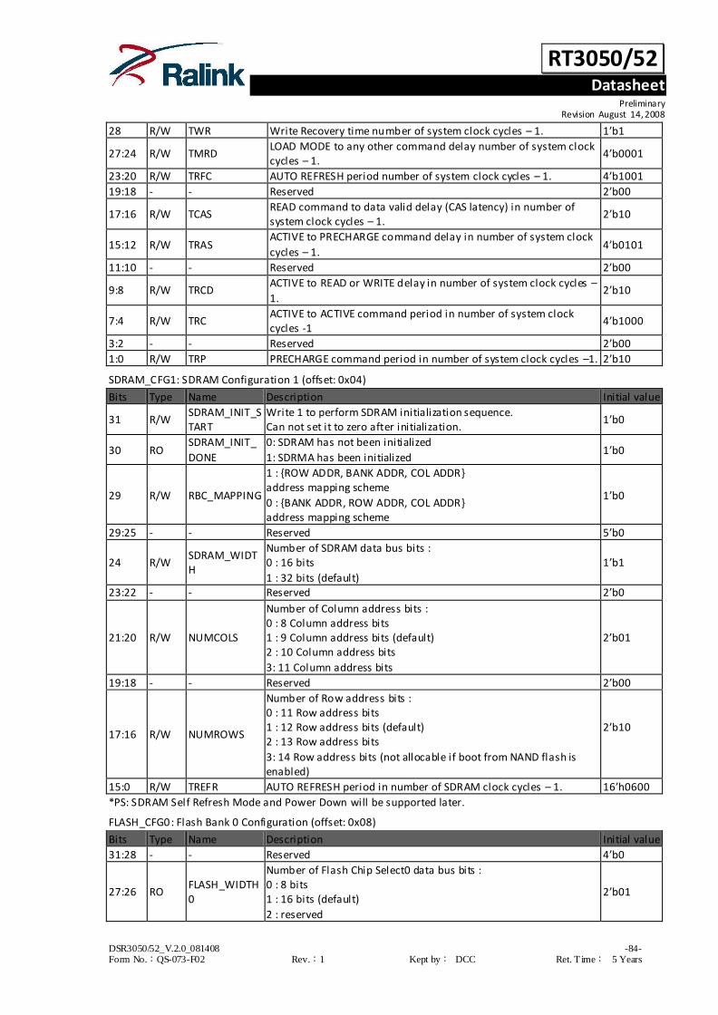
RT3050/52 Datasheet
Preliminary Revision August 14, 2008
DSR3050/52_V.2.0_081408 -84- Form No.:QS-073-F02 Rev.:1 Kept by: DCC Ret. T ime: 5 Years
28 R/W TWR Write Recovery time number of system clock cycles – 1. 1’b1
27:24 R/W TMRD LOAD MODE to any other command delay number of system clock cycles – 1.
4’b0001
23:20 R/W TRFC AUTO REFRESH period number of system clock cycles – 1. 4’b1001
19:18 - - Reserved 2’b00
17:16 R/W TCAS READ command to data valid delay (CAS latency) in number of system clock cycles – 1.
2’b10
15:12 R/W TRAS ACTIVE to PRECHARGE command delay in number of system clock
cycles – 1. 4’b0101
11:10 - - Reserved 2’b00
9:8 R/W TRCD ACTIVE to READ or WRITE delay in number of system clock cycles –
1. 2’b10
7:4 R/W TRC ACTIVE to ACTIVE command period in number of system clock cycles -1
4’b1000
3:2 - - Reserved 2’b00
1:0 R/W TRP PRECHARGE command period in number of system clock cycles –1. 2’b10
SDRAM_CFG1: SDRAM Configuration 1 (offset: 0x04)
Bits Type Name Description Initial value
31 R/W SDRAM_INIT_START
Write 1 to perform SDRAM initialization sequence. Can not set it to zero after initialization.
1’b0
30 RO SDRAM_INIT_
DONE
0: SDRAM has not been initialized
1: SDRMA has been initialized 1’b0
29 R/W RBC_MAPPING
1 : {ROW ADDR, BANK ADDR, COL ADDR} address mapping scheme
0 : {BANK ADDR, ROW ADDR, COL ADDR} address mapping scheme
1’b0
29:25 - - Reserved 5’b0
24 R/W SDRAM_WIDTH
Number of SDRAM data bus bits : 0 : 16 bits
1 : 32 bits (default)
1’b1
23:22 - - Reserved 2’b0
21:20 R/W NUMCOLS
Number of Column address bits : 0 : 8 Column address bits 1 : 9 Column address bits (default) 2 : 10 Column address bits
3: 11 Column address bits
2’b01
19:18 - - Reserved 2’b00
17:16 R/W NUMROWS
Number of Row address bits : 0 : 11 Row address bits 1 : 12 Row address bits (default) 2 : 13 Row address bits
3: 14 Row address bits (not allocable if boot from NAND flash is enabled)
2’b10
15:0 R/W TREFR AUTO REFRESH period in number of SDRAM clock cycles – 1. 16’h0600
*PS: SDRAM Self Refresh Mode and Power Down will be supported later.
FLASH_CFG0: Flash Bank 0 Configuration (offset: 0x08)
Bits Type Name Description Initial value
31:28 - - Reserved 4’b0
27:26 RO FLASH_WIDTH0
Number of Flash Chip Select0 data bus bits : 0 : 8 bits 1 : 16 bits (default)
2 : reserved
2’b01

RT3050/52 Datasheet
Preliminary Revision August 14, 2008
DSR3050/52_V.2.0_081408 -85- Form No.:QS-073-F02 Rev.:1 Kept by: DCC Ret. T ime: 5 Years
3 : reserved Note : This value is from boot strapping.
25 - - Reserved 1’b0
24 R/W CSADR0 Address hold time from Chip Select in number of system clock cycles
1’b1
23:22 - - Reserved 2’b0
21:20 R/W TWHOLD0 Chip select and Data hold time from Write Enable in number of system clock cycles
2’b01
19:18 - - Reserved 2’b0
17:16 R/W TRHOLD0 Chip select hold time from Output Enable in number of system clock cycles
2’b01
15:12 R/W TWE0 Write Enable duration in number of system clock cycles 4’b1111
11:8 R/W TOE0 Output Enable duration in number of system clock cycles 4’b1111
7:6 R/W TRADR0 Read address setup in number of system clock cycles 2’b10
5:4 R/W TWADR0 Write address setup in number of system clock cycles 2’b10
3:2 - - Reserved 2’b0
1:0 R/W TADRCS0 Address setup time prior to Chip Select in number of system clock cycles
2’b01
*PS: Flash_Width0 (8/16/32 bits) is configured by power on pin capture.
Note: Total of width specified by TADRCS + TWADR/TRADR + TWE/TOE + TWHOLD/TRHOLD + TCSADR may not be
fewer than 3 clock cycles.
MD
CS_N
WE_N
TADRCS
TWADR
TWE
TWHOLD
TCSADR
MD
CS_N
OE_N
TADRCS
TRADR
TOE
TRHOLD
TCSADR
MA,
WDATA
WADDR
MAWADDR
RDATA
Flash, Async. SRAM Write Timing
Flash, Async. SRAM Read Timing
Fig. 3-15-2 Flash/SRAM/SDRAM Controller R/W waveform
Note : Total of width specified by TADRCS + TWADR/TRADR + TWE/TOE + TWHOLD/TRHOLD + TCSADR may not
be fewer than 3 clock cycles
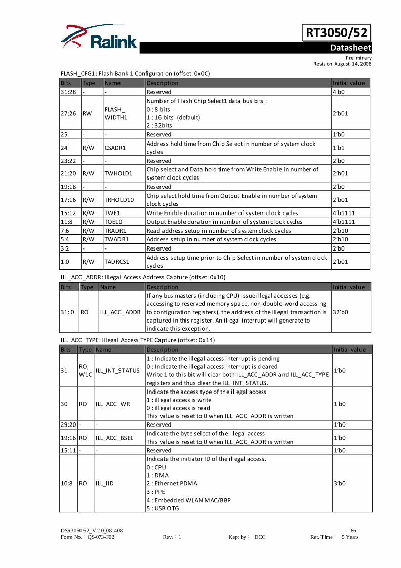
RT3050/52 Datasheet
Preliminary Revision August 14, 2008
DSR3050/52_V.2.0_081408 -86- Form No.:QS-073-F02 Rev.:1 Kept by: DCC Ret. T ime: 5 Years
FLASH_CFG1: Flash Bank 1 Configuration (offset: 0x0C)
Bits Type Name Description Initial value
31:28 - - Reserved 4’b0
27:26 RW FLASH_ WIDTH1
Number of Flash Chip Select1 data bus bits : 0 : 8 bits 1 : 16 bits (default) 2 : 32bits
2’b01
25 - - Reserved 1’b0
24 R/W CSADR1 Address hold time from Chip Select in number of system clock cycles
1’b1
23:22 - - Reserved 2’b0
21:20 R/W TWHOLD1 Chip select and Data hold time from Write Enable in number of system clock cycles
2’b01
19:18 - - Reserved 2’b0
17:16 R/W TRHOLD10 Chip select hold time from Output Enable in number of system clock cycles
2’b01
15:12 R/W TWE1 Write Enable duration in number of system clock cycles 4’b1111
11:8 R/W TOE10 Output Enable duration in number of system clock cycles 4’b1111
7:6 R/W TRADR1 Read address setup in number of system clock cycles 2’b10
5:4 R/W TWADR1 Address setup in number of system clock cycles 2’b10
3:2 - - Reserved 2’b0
1:0 R/W TADRCS1 Address setup time prior to Chip Select in number of system clock cycles
2’b01
ILL_ACC_ADDR: Illegal Access Address Capture (offset: 0x10)
Bits Type Name Description Initial value
31: 0 RO ILL_ACC_ADDR
If any bus masters (including CPU) issue illegal accesses (e.g. accessing to reserved memory space, non-double-word accessing
to configuration registers), the address of the illegal transaction is captured in this register. An illegal interrupt will generate to indicate this exception.
32’b0
ILL_ACC_TYPE: Illegal Access TYPE Capture (offset: 0x14)
Bits Type Name Description Initial value
31 RO, W1C
ILL_INT_STATUS
1 : Indicate the illegal access interrupt is pending 0 : Indicate the illegal access interrupt is cleared Write 1 to this bit will clear both ILL_ACC_ADDR and ILL_ACC_TYPE
registers and thus clear the ILL_INT_STATUS.
1’b0
30 RO ILL_ACC_WR
Indicate the access type of the illegal access 1 : il legal access is write 0 : il legal access is read This value is reset to 0 when ILL_ACC_ADDR is written
1’b0
29:20 - - Reserved 1’b0
19:16 RO ILL_ACC_BSEL Indicate the byte select of the illegal access
This value is reset to 0 when ILL_ACC_ADDR is written 1’b0
15:11 - - Reserved 1’b0
10:8 RO ILL_IID
Indicate the initiator ID of the illegal access. 0 : CPU 1 : DMA 2 : Ethernet PDMA
3 : PPE 4 : Embedded WLAN MAC/BBP 5 : USB OTG
3’b0

RT3050/52 Datasheet
Preliminary Revision August 14, 2008
DSR3050/52_V.2.0_081408 -87- Form No.:QS-073-F02 Rev.:1 Kept by: DCC Ret. T ime: 5 Years
6-7 : Reserved This value is reset to 0 when ILL_ACC_ADDR is written
7:0 RO ILL_ACC_LEN Indicate the access size of the illegal access. The unit is byte
This value is reset to 0 when ILL_ACC_ADDR is written. 8’b0

RT3050/52 Datasheet
Preliminary Revision August 14, 2008
DSR3050/52_V.2.0_081408 -88- Form No.:QS-073-F02 Rev.:1 Kept by: DCC Ret. T ime: 5 Years
3.16 NAND Flash Controller
3.16.1 Features
Supports boot from NAND flash memory.
Supports read / erase / page program NAND flash memory.
Hardware ECC engine. (Hardware generating and software correcting)
The internal 4Kbytes boot buffer can be used for another application after booting.
Only supports NAND flash memory with 512-bytes page size and 8-bits data.
Indirect access for special command.
Configurable write protect register.
Little / bit ending operation.
3.16.2 Block Diagram
Boot Buffer
(4KB)
Control State
Machine
Registers /
Data Buffer
ECC
Encoder /
Decoder
NAND Flash
Interface
PBus
CLE
ALE
nCE
nWE
R/nB
I/O 0~7
GDMA
System
Reg
PCI
Arbitor
Buffer Control
Fig. 3-16-1 NAND Flash Controller Block Diagram
3.16.3 Register Description (base: 0x1000.0800)
CTRL: NAND Flash Control Register (offset: 0x00)
Bits Type Name Description Initial value
31:24 - - Reserved
23:16 RW TWAITB Dummy time period to wait busy signal = clock * (TWAIT+1) 0
15:12 RW THOLD Hold time duration = clock * (THOLD+1) 0
11:8 RW TPERIOD Period time duration = clock * (TPERIOD+1) 0
7:4 RW TSETUP Setup time duration = clock * (TSETUP+1) 0
3:2 RW BURST_SIZE 0: 1 DW 1: 2 DW 2: 4 DW 3: 8 DW
0
1 RW DBUF_CLR Clear data buffer 0
0 RW WP Write protect 0

RT3050/52 Datasheet
Preliminary Revision August 14, 2008
DSR3050/52_V.2.0_081408 -89- Form No.:QS-073-F02 Rev.:1 Kept by: DCC Ret. T ime: 5 Years
TRANS_CFG: Transfer Control Register (offset: 0x04)
Bits Type Name Description Initial value
31:30 - - Reserved
29:20 RW BNUM_DATA Byte number of data to be transferred 528
19 - - Reserved
18:16 RW BNUM_ADDR Byte number of address Note: maximum number is 4
3
15:14 - - Reserved
13:12 RW BNUM_CMD3 Byte number of command 3 0
11:10 RW BNUM_CMD2 Byte number of command 2 0
9:8 RW BNUM_CMD1 Byte number of command 1 1
7 RW RESPB_DATA Respect busy signal after data phase 0
6 RW RESPB_ADDR Respect busy signal after address phase 0
5 RW RESPB_CMD3 Respect busy signal after command 3 phase 0
4 RW RESPB_CMD2 Respect busy signal after command 2 phase 0
3 RW ECC_ENA ECC enable 0: disable 1: enable
Note: In read transfer, HW ECC check function will be active. In write transfer, HW ECC generate function will be active.
0
2 RW DMA_ENA Issue a request to generic DMA when data read/write. 0: CPU will get/put data from/to data buffer. 1: GDMA will get/put data from/to data buffer.
0
1 RW WR_TRANS The transfer is read / write.
0: read 1: write
0
0 WC KICK_TRANS Kick the a NAND flash transfer 0: no transfer 1: kick a transfer
Note: this bit will auto clear
0
CMD1: Command #1 Register (offset: 0x08)
Bits Type Name Description Initial value
31:24 - - Reserved
23:16 RW CMD1_BYTE3 3rd
byte of command 1 0
15:8 RW CMD1_BYTE2 2nd
byte of command 1 0
7:0 RW CMD1_BYTE1 1st
byte of command 1 0
CMD2: Command #2 Register (offset: 0x0C)
Bits Type Name Description Initial value
31:24 - - Reserved
23:16 RW CMD2_BYTE3 3rd
byte of command 2 0
15:8 RW CMD2_BYTE2 2nd
byte of command 2 0
7:0 RW CMD2_BYTE1 1st
byte of command 2 0
CMD3: Command #3 Register (offset: 0x10)
Bits Type Name Description Initial value
31:24 - - Reserved
23:16 RW CMD3_BYTE3 3rd
byte of command 3 0
15:8 RW CMD3_BYTE2 2nd
byte of command 3 0
7:0 RW CMD3_BYTE1 1st
byte of command 3 0
ADDR: Address Register (offset: 0x14)
Bits Type Name Description Initial value
31:24 RW ADD_BYTE4 4th
byte of address

RT3050/52 Datasheet
Preliminary Revision August 14, 2008
DSR3050/52_V.2.0_081408 -90- Form No.:QS-073-F02 Rev.:1 Kept by: DCC Ret. T ime: 5 Years
23:16 RW ADD_BYTE3 3rd
byte of address 0
15:8 RW ADD_BYTE2 2nd
byte of address 0
7:0 RW ADD_BYTE1 1st
byte of address 0
DATA: Data Register (offset: 0x18)
Bits Type Name Description Initial value
31:0 RW DATA Data for read / write 0
ECC_ENC: ECC Encode Register (offset: 0x1C)
Bits Type Name Description Initial value
31:24 - - Reserved -
23:16 R ENC_BYTE2 3rd
byte of ECC encode 0
15:8 R ENC_BYTE1 2nd
byte of ECC encode 0
7:0 R ENC_BYTE0 1st
byte of ECC encode 0
STATUS: Status Register (offset: 0x20)
Bits Type Name Description Initial value
31:17 - - Reserved -
16:8 R DEC_BYTE ECC decode fail byte address 0
7 - - Reserved
6:4 R DEC_BIT ECC decode fail bit address 0
3 - - Reserved
2 R ND_RB_N NAND flash ready 0: busy 1: ready
1
1 R DEC_ERR ECC decode check status
0: no error 1: correctable error or ecc error
0
0 R BUSY NAND flash controller is in busy. 0: idle 1: busy
0
INT_STATUS (offset: 0x0c, default: 0x00)
Bits Type Name Description Initial value
31:8 - - Reserved -
7 W1C RX_KICK_ERR Rx buffer not empty at host kick 0 6 W1C TX_KICK_ERR Tx buffer not empty at host kick 0
5 W1C RX_TRAS_ERR Rx buffer not empty at transfer done 0
4 W1C TX_TRAS_ERR Tx buffer not empty at transfer done 0
3 W1C ECC_ERR ECC error 0
2 W1C RX_BUF_RDY Rx buffer read ready 0
1 W1C TX_BUF_RDY Tx buffer write ready 0
0 W1C ND_DONE Transfer done 0

RT3050/52 Datasheet
Preliminary Revision August 14, 2008
DSR3050/52_V.2.0_081408 -91- Form No.:QS-073-F02 Rev.:1 Kept by: DCC Ret. T ime: 5 Years
3.17 Frame Engine
3.17.1 Features
Wire-speed (1000Mbps) Ethernet LAN/WAN NAT/NAPT routing
L1-L7(content aware) policy table
QoS support for multimedia traffic
Support per flow/rule accounting/rate limiting
Checksum/VLAN/PPPoE offload
3.17.1.1 Network Interfaces
One 10/100/1000Mbps Ethernet MACs with RGMII/MII interfaces
One Scatter-Gather packet DMA with Rbus master interface
One special port for packet processing engine
3.17.1.2 PSE (Packet Switch Engine) Features
Four external ports and one special PPE port (for packet bridging/routing)
Efficient page-based buffer management
QoS-aware queue management
Supports 4 output queues/virtual WAN/LAN port
WRR/Strict priority scheduling
Egress rate limiting/shaping
Non-blocking, wire-speed packet switching
Flow control for no-packet-loss guarantee
Emulated multicast support (can mirror a TX packet to CPU)
Checksum offload, VLAN & PPPOE header insertion (by CDMA)
Auto-Padding for sub-64B packets
3.17.1.3 PPE Features
Supports 512 policy rules for ACL, accounting and rate limiting.
The policy rules can base on pre-route/post-route L1-L7 headers & contents (up-to 16 bytes)
DDoS avoidance by rate limiting
Supports stateful packet filtering (SPI)
Supports IPv4 NAT/NAPT routing
Supports 1/2/4/8/16K IPv4 NAPT flows
Supports virtual server, port-triggering & port forwarding
Supports any kind of IPv4 NAT(NAPT, Twice NAT)
Supports 16 PPPoE sessions
Supports cone-NAT, port-restricted NAT & Symmetric NAT
Supports per rule or per flow accounting or rate l imiting
Patent-pending Flow Offloading technology for flexible/high performance packet L3/L4 packet
processing
Supports double VLAN tagging (Q-in-Q)
Support VID Swapping
Support multi-WAN load balancing with H/W S/W cooperation
PS : All the PPE features mentioned above require software porting to enable.

RT3050/52 Datasheet
Preliminary Revision August 14, 2008
DSR3050/52_V.2.0_081408 -92- Form No.:QS-073-F02 Rev.:1 Kept by: DCC Ret. T ime: 5 Years
3.17.1.4 QoS Related Features
Packets can be classified based on L1-L7 headers/content
Supports 4 TX queues
Supports WRR scheduling for the two virtual WAN and LAN ports
Supports egress rate limiting for each network port
Powerful buffer reservation scheme to reserve packet buffer resources for multi -media traffic.
3.17.1.5 Packet DMA (PDMA) Features
Supports 4 TX descriptor rings and one RX descriptor ring
Scatter/Gather DMA
Delayed interrupt
Configurable 4/8/16 32-bit word burst length
3.17.2 Block Diagram
PSE(Packet Switching Engine)
PPE(Packet Processing Engine)
GDMA 1 (LAN)GDMA2 (WAN)
CDMA
PDMA
Embedded Swithc (1 GE + 5 FE ports)
High Speed Bus
Slow Bus
Ingress ParsingEgress Schedule/Egress Rate Limiting
Checksum Offload
Scatter/GatheringDMA
NAT/NAPT/SPI/FirewallRate Limiting/Accounting
Generic Packet Switch Fabric
CPU port (Port #0)
Fig. 3-17-1 Frame Engine Block Diagram

RT3050/52 Datasheet
Preliminary Revision August 14, 2008
DSR3050/52_V.2.0_081408 -93- Form No.:QS-073-F02 Rev.:1 Kept by: DCC Ret. T ime: 5 Years
3.17.2.1 PDMA FIFO-like Ring Concept
Fig. 3-17-2 PDMA FIFO-like Ring Concept
3
1 0
Byte 0 Byte 1 Byte 2 Byte 3
ICO : IP checksum offload enable
UDP : UDP checksum offload enable
TCO : TCP checksum offload enable
PN : Destination port Number
(0 : CPU, 1 : GDMA #1, 2: GDMA #2,
3-5 : Reserved, 6 : PPE, 7 : Discard )
QN : Destination Queue Number
UDF : User define field
INSP : Insert PPPoE header
SIDX : PPPoE Session index
INSV : Insert VLAN tag
VPRI : VLAN priority tag to be inserted
VIDX : VLAN ID Index
SDP : Segment Data Pointer
SDL : Segment Data Length
LS : Last Segment
DDONE : DMA Done. Indicate DMA
has transfer the segment pointed by
this TX descriptor
Burst : when set, the scheduler can
not hand-over to other TS queues.
Should go on to transmit the next
packet
SDL0[13:0]
T
C
O
U
C
O
I
C
O
SDP0[30:0]
D
D
O
N
E
L
S
0
QN
[2:0]
PN
[2:0]00 VIDX[3:0]
I
N
S
V
I
N
S
P
SIDX[3:0]The DWORD is
called TXINFO
SDP1[30:0]
SDL1[13:0]
L
S
1
VPRI
[2:0]5'00000 0 0
U
D
F
B
U
R
S
T

RT3050/52 Datasheet
Preliminary Revision August 14, 2008
DSR3050/52_V.2.0_081408 -94- Form No.:QS-073-F02 Rev.:1 Kept by: DCC Ret. T ime: 5 Years
3.17.2.2 PDMA Descriptor Format
Fig. 3-17-3 PDMA TX Descriptor Format
RX_DONE_INT(j)
RX_DMA_BUSY
RX_DMA_EN
TX_CRLS_IDX(i)*
(points to non-released TSD)
RX_CALC_IDX(j)
(points to non- allocated FSD)
(points to non- received DMA FSD)
(points to non- received CPU FSD)
TX_DTX_IDX(i)
(points to non transmitted DMA TSD)
(points to non- transmitted CPU TSD) RX
_M
AX_C
NT
TX_
MA
X_C
NT
Tx _ pkt # l Tx _ pkt # k Tx _ pkt # j
Tx _ pkt # i
TX_DMA
Rx _ pkt # a
Rx _ pkt # b
Rx _ pkt # c
RX_DMA
Rx _ pkt # d
TX_Driver
TX_Driver
( i = 0 - 3 ) ( j = 0 )
PDMA / Frame Engine
Software Driver
TX_CTX_IDX(i)
RX_CRX_IDX(j)
RX_DRX_IDX(j)
TX_DMA_EN
TX_DMA_BUSY
TX_DMNE_INT(i)
PDMA_DLY_INT
Note1: TX_CRLSIDX(i) and RX_CRXIDX(i) are not in PDMA hardware they are resident in CPUs Local memory
Note2:
TXQ0: GE Mac low queue RXQ0: For GE MAC receive TXQ1: GE Mac high queue

RT3050/52 Datasheet
Preliminary Revision August 14, 2008
DSR3050/52_V.2.0_081408 -95- Form No.:QS-073-F02 Rev.:1 Kept by: DCC Ret. T ime: 5 Years
Fig. 3-17-4 PDMA RX Descriptor Format
3.17.3 Register Description (base: 0x1010.0000)
3.17.3.1 Register Description -GE Port (base: 0x1010.0000)
MDIO_ACCESS: MDIO Access (offset: 0x00)
Bits Type Name Description Initial value
31 WSC MD_CMD_TRG
MDIO command trigger. This bit is cleared by hardware after
command is completed. 1 : Read/write operation ongoing 0 : Read/write operation complete
1’b0
30 WO MD_WR
When set, this bit tells the PHY that this will be a Write operation using MD_DATA register. If this bit is not set, this will
be a Read operation, placing the data in MD_DATA register. 1 : Write operation. 0 : Read operation.
1’b0
29 - - Reserved 1’b0
28:24 R/W MD_PHY_ADDR Address of PHY device 5’b0
23:21 - - Reserved 3’b0
20:16 R/W MD_REG_ADDR Register addresses within PHY device 5’b0
15:0 R/W MD_DATA PHY register read/write data 16’b0
MDIO_CFG1:Reserved (offset: 0x04)
FE_GLO_CFG: Frame Engine Global Configuration (offset: 0x08)
Bits Type Name Description Initial value
31:16 R/W EXT_VLAN Extended VLAN type 16’h8100
15:8 R/W US_CYC_CNT 1us timer count in unit of clock cycle. For example, if frame
engine is running at 133MHz, set this register to 8’d132. 8’d132
7:4 R/W L2_SPACE L2 space. Unit is 8 bytes 4’h8
3:0 - - Reserved 1’b0
3
1 0
Byte 0
Byte 1 Byte 2 Byte 3
SDP0 : Segment Data Pointer for hdr (if hp_sep_en=1) or the
whole pkt (if hp_sep_en = 0)
SDP1 : Segment Data Pointer for payload (valid when hp_seg_len!=0)
SDL0 : RXWI + Packet hdr length (ifhp_seg_len!=0), or RXWI + Pkt len (if
hp_seg_len!=0)
SDL1 : =payload length (if hp_seg_len!=0)
DDONE : DMA Done. Indicate DMA
has received the segments
pointed by this RX descriptor
SDL0[13:0]
SDP0[31:0]
L
S
0
The DWORD is
called RXINFO
SDP1[31:0]
D
D
O
N
E
Byte 3
SDL1[13:0]10
IPFVLD : IPv4 & (Hlen==5)
L4FVLD : IPFVLD & No IP frag & (TCP|UDP)
IPF : IP Checksum Fail
L4F : L4 Checksum Fail
AIS : Assist Info Select
AI : Assist Info
Par_Rlt(AIS=0) : Parser Result form Port
CPU_Reason (AIS=1) : CPU reason from PPE to CPU
FVLD : FOE_Entry valid
L
4
F
I
P
F
I
P
F
V
L
D
L
4
F
V
L
D
FOE_Entry[13:0]
F
V
L
D
AI
(Par_Rlt[7:0]/CPU_Rea
son[7:0)
SP
[2:0]
A
I
S
0

RT3050/52 Datasheet
Preliminary Revision August 14, 2008
DSR3050/52_V.2.0_081408 -96- Form No.:QS-073-F02 Rev.:1 Kept by: DCC Ret. T ime: 5 Years
FE_RST_GLO: Frame Engine Global Reset (offset: 0x0C)
Bits Type Name Description Initial value
31:16 RC FC_DROP_CNT Flow control drop packet count. 16’b0
15:1 - - Reserved 15’b0
0 WO PSE_RESET PSE reset Write 1 to reset PSE Write 0 to disable reset PSE
1’b0
FE_INT_STATUS: Frame Engine Interrupt Status (offset: 0x10)
Bits Type Name Description Initial value
31 R/W CNT_PPE_AF PPE Counter Table Almost Full Write 1 to clear the interrupt. Read to get the raw interrupt status
1’b0
30 - - Reserved 1’b0
29 R/W CNT_GDM_AF GDMA 1 &2 Counter Table Almost Full Write 1 to clear the interrupt.
Read to get the raw interrupt status
1’b0
28:25 - - Reserved 4’b0
26 R/W PSE_P2_FC PSE port2 (GDMA 2) flow control asserted. Write 1 to clear the interrupt. Read to get the raw interrupt status
1’b0
25 R/W GDM_CRC_DROP GDMA 1 & 2 discard a packet due to CRC error Write 1 to clear the interrupt.
Read to get the raw interrupt status
1’b0
24 R/W PSE_BUF_DROP
PSE discards a packet due to buffer sharing limitation (flow control) Write 1 to clear the interrupt. Read to get the raw interrupt status
1’b0
23 R/W GDM_OTHER_DROP
GDMA 1 & 2 discard a packet due to other reason (e.g. too
short, too long, FIFO overflow, checksum error,.., etc.) Write 1 to clear the interrupt. Read to get the raw interrupt status
1’b0
22 R/W PSE_P1_FC PSE port1 (GDMA 1) flow control asserted. Write 1 to clear the interrupt.
Read to get the raw interrupt status
1’b0
21 R/W PSE_P0_FC PSE port0 (CDMA) flow control asserted. Write 1 to clear the interrupt. Read to get the raw interrupt status
1’b0
20 R/W PSE_FQ_EMPTY
PSE free Q empty threshold reached & forced drop condition occurred.
Write 1 to clear the interrupt. Read to get the raw interrupt status
1’b0
17 R/W TX_COHERENT TX_DMA finds data coherent event when checking ddone bit. Write 1 to clear the interrupt. Read to get the raw interrupt status
1’b0
16 R/W RX_COHERENT
RX_DMA finds data coherent event when checking ddone bit.
Write 1 to clear the interrupt. Read to get the raw interrupt status
1’b0
15:12 - - Reserved 4’b0
11 R/W TX_DONE_INT3 Tx queue#3 packet transmit interrupt Write 1 to clear the interrupt. Read to get the raw interrupt status
1’b0
10 R/W TX_DONE_INT2 Tx queue#2 packet transmit interrupt
Write 1 to clear the interrupt. 1’b0

RT3050/52 Datasheet
Preliminary Revision August 14, 2008
DSR3050/52_V.2.0_081408 -97- Form No.:QS-073-F02 Rev.:1 Kept by: DCC Ret. T ime: 5 Years
Read to get the raw interrupt status
9 R/W TX_DONE_INT1 Tx queue#1 packet transmit interrupt Write 1 to clear the interrupt. Read to get the raw interrupt status
1’b0
8 R/W TX_DONE_INT0
Tx queue#0 packet transmit interrupt
Write 1 to clear the interrupt. Read to get the raw interrupt status
1’b0
7:3 - - Reserved 5’b0
2 R/W RX_DONE_INT0 Packet receive interrupt. Write 1 to clear the interrupt. Read to get the raw interrupt status
1’b0
1 R/W TX_DLY_INT
Delayed version of TX_DONE_INT0 and TX_DONE_INT1. Write 1
to clear the interrupt. Read to get the raw interrupt status
1’b0
0 R/W RX_DLY_INT Delayed version of RX_DONE_INT0. Write 1 to clear the interrupt. Read to get the raw interrupt status
1’b0
FE_INT_ENABLE: Frame Engine Interrupt Enable (offset: 0x14)
Bits Type Name Description Initial value
31 R/W CNT_PPE_AF PPE Counter Table Almost Full 1 : Enable the interrupt 0 : Disable the interrupt
1’b0
30 - - Reserved 1’b0
29 R/W CNT_GDM_AF GDMA 1 & 2 Counter Table Almost Full Write 1 to clear the interrupt.
Read to get the raw interrupt status
1’b0
28:27 - - Reserved 2’b0
26 R/W PSE_P2_FC
PSE port2 (GDMA2) flow control asserted.
1 : Enable the interrupt 0 : Disable the interrupt
1’b0
25 - - Reserved 1’b0
24 R/W PSE_BUF_DROP
PSE discards a packet due to buffer sharing limitation (flow control) 1 : Enable the interrupt
0 : Disable the interrupt
1’b0
23 R/W GDM_OTHER_ DROP
GDMA 1 & 2 discard a packet due to other reason (e.g. too short, too long, FIFO overflow, checksum error,.., etc.) 1 : Enable the interrupt 0 : Disable the interrupt
1’b0
22 R/W PSE_P1_FC
PSE port1 (GDMA1) flow control asserted.
1 : Enable the interrupt 0 : Disable the interrupt
1’b0
21 R/W PSE_P0_FC PSE port0 (CDMA) flow control asserted. 1 : Enable the interrupt 0 : Disable the interrupt
1’b0
20 R/W PSE_FQ_EMPTY
PSE free Q empty threshold reached & forced drop condition
occurred. 1 : Enable the interrupt 0 : Disable the interrupt
1’b0
19-18 - - Reserved 2’b0
17 R/W TX_COHERENT TX_DMA finds data coherent event when checking ddone bit. 1 : Enable the interrupt
0 : Disable the interrupt
1’b0

RT3050/52 Datasheet
Preliminary Revision August 14, 2008
DSR3050/52_V.2.0_081408 -98- Form No.:QS-073-F02 Rev.:1 Kept by: DCC Ret. T ime: 5 Years
16 R/W RX_COHERENT
RX_DMA finds data coherent event when checking ddone bit.
1 : Enable the interrupt 0 : Disable the interrupt
1’b0
15:12 - - Reserved 4’b0
11 R/W TX_DONE_INT3 Tx queue#3 packet transmit interrupt 1 : Enable the interrupt 0 : Disable the interrupt
1’b0
10 R/W TX_DONE_INT2
Tx queue#2 packet transmit interrupt
1 : Enable the interrupt 0 : Disable the interrupt
1’b0
9 R/W TX_DONE_INT1 Tx queue#1 packet transmit interrupt 1 : Enable the interrupt 0 : Disable the interrupt
1’b0
8 R/W TX_DONE_INT0 Tx queue#0 packet transmit interrupt 1 : Enable the interrupt 0 : Disable the interrupt
1’b0
7:3 - - Reserved 5’b0
2 R/W RX_DONE_INT0 Packet receives interrupt. 1 : Enable the interrupt 0 : Disable the interrupt
1’b0
1 R/W TX_DLY_INT Delayed version of TX_DONE_INT0 and 1 : Enable the interrupt
0 : Disable the interrupt 1’b0
0 R/W RX_DLY_INT Delayed version of RX_DONE_INT0. 1 : Enable the interrupt 0 : Disable the interrupt
1’b0
MDIO_CFG2:Reserved (offset: 0x 18)
FOE_TS_T: Time Stamp (offset: 0x1C)
Bits Type Name Description Initial value
31:24 R PSE_FQ_PCNT PSE free Q page count 8’hff
23:16 - - Reserved 8’b0
15:0 R/W FOE_TS_T Time stamp Note: Time Stamp unit is 1 sec.
16’b0
3.17.3.2 Register Description – GDMA 1 & 2 (base: 0x1010.0020)
GDMA_FWD_CFG: GDMA Forwarding Configuration (offset: 0x00)
Bits Type Name Description Initial value
31:24 - - Reserved 8’b0
23 R/W GDM_DROP_256B
A Special mode to drop packets with payload > 256 bytes. 0 : Drop packets according to standard Ethernet frame length
limitation. 1 : Drop packets with payload >256 bytes
1’b0
22 R/W GDM_ICS_EN IPv4 header checksum check enable 1’b1
21 R/W GDM_TCS_EN TCP checksum check enable 1’b1
20 R/W GDM_UCS_EN UDP checksum check enable 1’b1
19 R/W - Reserved 1’b0
18 R/W GDM_DISPAD 0 : Enable GDMA 1 & 2 Tx padding function. 1 : Disable GDMA 1 & 2 Tx padding function.
1’b0
17 R/W GDM_DISCRC 0 : Enable GDMA 1 & 2 Tx CRC generation. 1 : Disable GDMA 1 & 2 Tx CRC generation.
1’b0
16 R/W GDM_STRPCRC 0 : Disable GDMA 1 & 2 automatic Rx CRC stripping 1 : Enable GDMA 1 & 2 automatic Rx CRC stripping
1’b1
15 - - Reserved 1’b0

RT3050/52 Datasheet
Preliminary Revision August 14, 2008
DSR3050/52_V.2.0_081408 -99- Form No.:QS-073-F02 Rev.:1 Kept by: DCC Ret. T ime: 5 Years
14:12 R/W GDM_UFRC_P
GDMA1 & 2 My MAC uni -cast frames destination port 3’d0 : CPU
3’d1 : GDMA1 3’d2 : GDMA2 3’d6 : PPE 3’d7 : Discard
Others: Reserved
3’b111
11 - - Reserved 1’b0
10:8 R/W GDM_BFRC_P
GDMA1 & 2 broadcast MAC address frames destination port 3’d0 : CPU 3’d1 : GDMA1 3’d2 : GDMA2
3’d6 : PPE 3’d7 : Discard Others: Reserved
3’b111
7 - - Reserved 1’b0
6:4 R/W GDM_MFRC_P
GDMA1 & 2 multi -cast MAC address frames destination port 3’d0 : CPU
3’d1 : GDMA1 3’d2 : GDMA2 3’d6 : PPE 3’d7 : Discard
Others: Reserved
3’b111
3 - - Reserved 1’b0
2:0 R/W GDM_OFRC_P
GDMA1 & 2 other MAC address frames destination port 3’d0 : CPU 3’d1 : GDMA1 3’d2 : GDMA2
3’d6 : PPE 3’d7 : Discard Others: Reserved
3’b111
GDMA1_SCH_CFG: GDMA1 Scheduling Configuration (offset: 0x04)
Bits Type Name Description Initial value
31:26 - - Reserved 7’b0
25:24 R/W GDM1_SCH_MOD
2’b00 : WRR
2’b01 : Strict Priority, Q3>Q2>Q1>Q0 2’b10 : Mixed, Q3>WRR(Q2,Q1,Q0) 2’b11 : Reserved
2’b00
23:15 - - Reserved 1’b0
14:12 R/W GDM1_WT_Q3
Q3’s weight
3’d0 : weight = 1 3’d1 : weight = 2 3’d2 : weight = 4 3’d3 : weight = 8
3’d4 : weight = 16
3’b011
11 - - Reserved 1’b0
10:8 R/W GDM1_WT_Q2
Q2’s weight
3’d0 : weight = 1 3’d1 : weight = 2 3’d2 : weight = 4 3’d3 : weight = 8
3’d4 : weight = 16
3’b010
7 - - Reserved 1’b0

RT3050/52 Datasheet
Preliminary Revision August 14, 2008
DSR3050/52_V.2.0_081408 -100- Form No.:QS-073-F02 Rev.:1 Kept by: DCC Ret. T ime: 5 Years
6:4 R/W GDM1_WT_Q1
Q1’s weight 3’d0 : weight = 1
3’d1 : weight = 2 3’d2 : weight = 4 3’d3 : weight = 8 3’d4 : weight = 16
3’b001
3 - - Reserved 1’b0
2:0 R/W GDM1_WT_Q0
Q0’s weight
3’d0 : weight = 1 3’d1 : weight = 2 3’d2 : weight = 4 3’d3 : weight = 8
3’d4 : weight = 16
3’b0
GDMA1_SHPR_CFG: GDMA1 Output Shaper Configuration (offset: 0x08)
Bits Type Name Description Initial value
31:25 - - Reserved 7’b0
24 R/W GDM1_SHPR_EN GDMA1 output shaper enable. 0 : Disable 1 : Enable
1’b0
23:16 R/W GDM1_BK_SIZE GDMA1 output shaper maximum bucket size. Unit is 1kB. 8’b0
15:14 - - Reserved 2’b0
13:0 R/W GDM1_TK_RATE GDMA1 output shaper token rate. Unit is 8B/ms. 14’b0
GDMA_MAC_ADRL: GDMA 1 & 2 MAC Address LSB (offset: 0x0C)
Bits Type Name Description Initial value
31:0 R/W GDM1_MY_MAC_L GDMA 1 & 2 MAC address bit 31-0 32’b0
GDMA_MAC_ADRH: GDMA 1 & 2 MAC Address MSB (offset: 0x10)
Bits Type Name Description Initial value
31:16 - - Reserved 16’b0
15:0 R/W GDM1_MY_MAC_H
GDMA 1 & 2 MAC address bit 47-32 16’b0
3.17.3.3 Register Description - PSE (base: 0x1010.0040)
PSE_FQ_CFG: PSE_FQ_CFG Register (offset:0x00)
Bits Type Name Description Initial value
31:24 R/W FQ_MAX_PCNT Maximum free Q page count. Please reset PSE after re-programming this register.
8’h80
23:16 R/W FQ_FC_RLS Free Q flow control release threshold. 8’h50
15:8 R/W FQ_FC_ASRT Free Q flow control assertion threshold. 8’h40
7:0 R/W FQ_FC_DROP
Free Q empty threshold. If one input port is FC asserted and
this threshold is reached, PSE will drop any new coming frame from this port.
8’h00
CDMA_FC_CFG: CDMA_FC_CFG Register (offset:0x04)
Bits Type Name Description Initial value
31:29 - - Reserved 3’b0
28 R/W P0_SHARING Allows high priority Q to share low priority Q’s reserved pages. 1: enable
0: disable
1’b1

RT3050/52 Datasheet
Preliminary Revision August 14, 2008
DSR3050/52_V.2.0_081408 -101- Form No.:QS-073-F02 Rev.:1 Kept by: DCC Ret. T ime: 5 Years
27:24 R/W P0_HQ_DEF
Bit map definition of high priority Q. ‘1’ presents high priority Q, and ‘0’ presents low priority Q.
bit 27: Q3 priority definition bit 26: Q2 priority definition bit 25: Q1 priority definition bit 24: Q0 priority definition
4’b1100
23:16 R/W P0_HQ_RESV Reserved page count for high priority Q. 8’h10
15:8 R/W P0_LQ_RESV Reserved page count for low priority Q. 8’h10
7:0 R/W P0_IQ_ASRT Virtual input Q FC assertion threshold. 8’h10
GDMA1_FC_CFG: GDMA1_FC_CFG Register (offset:0x08)
Bits Type Name Description Initial value
31:29 - - Reserved 3’b0
28 R/W P1_SHARING
Allows high priority Q to share low priority Q’s reserved pages.
1: enable 0: disable
1’b1
27:24 R/W P1_HQ_DEF
Bit map definition of high priority Q. ‘1’ presents high priority Q, and ‘0’ presents low priority Q. bit 27: Q3 priority definition
bit 26: Q2 priority definition bit 25: Q1 priority definition bit 24: Q0 priority definition
4’b1100
23:16 R/W P1_HQ_RESV Reserved page count for high priority Q. 8’h10
15:8 R/W P1_LQ_RESV Reserved page count for low priority Q. 8’h10
7:0 R/W P1_IQ_ASRT Virtual input Q FC assertion threshold. 8’h10
GDMA2_FC_CFG: GDMA2_FC_CFG Register (offset:0x0C)
Bits Type Name Description Initial value
31:29 - - Reserved 3’b0
28 R/W P2_SHARING Allows high priority Q to share low priority Q’s reserved pages. 1: enable 0: disable
1’b1
27:24 R/W P2_HQ_DEF
Bit map definition of high priority Q. ‘1’ presents high priority Q, and ‘0’ presents low priority Q.
bit 27: Q3 priority definition bit 26: Q2 priority definition bit 25: Q1 priority definition bit 24: Q0 priority definition
4’b1100
23:16 R/W P2_HQ_RESV Reserved page count for high priority Q. 8’h10
15:8 R/W P2_LQ_RESV Reserved page count for low priority Q. 8’h10
7:0 R/W P2_IQ_ASRT Virtual input Q FC assertion threshold. 8’h10
CDMA_OQ_STA: CDMA_OQ_STA Register (offset:0x10)
Bits Type Name Description Initial value
31:24 RO P0_OQ3_PCNT CDMA output Q3 page count. 8’b0
23:16 RO P0_OQ2_PCNT CDMA output Q2 page count. 8’b0
15:8 RO P0_OQ1_PCNT CDMA output Q1 page count. 8’b0
7:0 RO P0_OQ0_PCNT CDMA output Q0 page count. 8’b0
GDMA1_OQ_STA: GDMA1_OQ_STA Register (offset:0x14)
Bits Type Name Description Initial value
31:24 RO P1_OQ3_PCNT GDMA1 output Q3 page count. 8’b0
23:16 RO P1_OQ2_PCNT GDMA1 output Q2 page count. 8’b0
15:8 RO P1_OQ1_PCNT GDMA1 output Q1 page count. 8’b0
7:0 RO P1_OQ0_PCNT GDMA1 output Q0 page count. 8’b0

RT3050/52 Datasheet
Preliminary Revision August 14, 2008
DSR3050/52_V.2.0_081408 -102- Form No.:QS-073-F02 Rev.:1 Kept by: DCC Ret. T ime: 5 Years
GDMA2_OQ_STA: GDMA2_OQ_STA Register (offset:0x18)
Bits Type Name Description Initial value
31:24 RO P2_OQ3_PCNT GDMA2 output Q3 page count. 8’b0
23:16 RO P2_OQ2_PCNT GDMA2 output Q2 page count. 8’b0
15:8 RO P2_OQ1_PCNT GDMA2 output Q1 page count. 8’b0
7:0 RO P2_OQ0_PCNT GDMA2 output Q0 page count. 8’b0
PSE_IQ_STA: PSE_IQ_STA Register (offset:0x1C)
Bits Type Name Description Initial value
31:24 RO P6_OQ0_PCNT PPE output Q0 page count. 8’b0
23:16 RO P2_IQ_PCNT GDMA2 virtual input Q page count. 8’b0
15:8 RO P1_IQ_PCNT GDMA1 virtual input Q page count. 8’b0
7:0 RO P0_IQ_PCNT CDMA virtual input Q page count. 8’b0
3.17.3.4 Register Description – GDMA2 (base: 0x1010.0060)
GDMA2_FWD_CFG: Reserved (offset: 0x00)
GDMA2_SCH_CFG: GDMA2 Scheduling Configuration (offset: 0x04)
Bits Type Name Description Initial value
31:26 - - Reserved 7’b0
25:24 R/W GDM2_SCH_MOD
2’b00 : WRR 2’b01 : Strict Priority, Q3>Q2>Q1>Q0
2’b10 : Mixed, Q3>WRR(Q2,Q1,Q0) 2’b11 : Reserved
2’b00
23:15 - - Reserved 1’b0
14:12 R/W GDM2_WT_Q3
Q3’s weight 3’d0 : weight = 1 3’d1 : weight = 2
3’d2 : weight = 4 3’d3 : weight = 8 3’d4 : weight = 16
3’b011
11 - - Reserved 1’b0
10:8 R/W GDM2_WT_Q2
Q2’s weight 3’d0 : weight = 1
3’d1 : weight = 2 3’d2 : weight = 4 3’d3 : weight = 8
3’d4 : weight = 16
3’b010
7 - - Reserved 1’b0
6:4 R/W GDM2_WT_Q1
Q1’s weight
3’d0 : weight = 1 3’d1 : weight = 2 3’d2 : weight = 4
3’d3 : weight = 8 3’d4 : weight = 16
3’b001
3 - - Reserved 1’b0
2:0 R/W GDM2_WT_Q0
Q0’s weight 3’d0 : weight = 1 3’d1 : weight = 2
3’d2 : weight = 4 3’d3 : weight = 8 3’d4 : weight = 16
3’b0

RT3050/52 Datasheet
Preliminary Revision August 14, 2008
DSR3050/52_V.2.0_081408 -103- Form No.:QS-073-F02 Rev.:1 Kept by: DCC Ret. T ime: 5 Years
GDMA2_SHPR_CFG: GDMA2 Output Shaper Configuration (offset: 0x08)
Bits Type Name Description Initial value
31:25 - - Reserved 7’b0
24 R/W GDM2_SHPR_EN GDMA2 output shaper enable. 0 : Disable
1 : Enable
1’b0
23:16 R/W GDM2_BK_SIZE GDMA2 output shaper maximum bucket size. Unit is 1kB. 8’b0
15:14 - - Reserved 2’b0
13:0 R/W GDM2_TK_RATE GDMA2 output shaper token rate. Unit is 8B/ms. 14’b0
3.17.3.5 Register Description - CPU Port (base:0x1010.0080)
CDMA_CSG_CFG: CDMA_CSG_CFG Register (offset: 0x00)
Bits Type Name Description Initial value
31:16 R/W INS_VLAN_ Inserted VLAN type 16’h8100
15:3 - - Reserved 13’b0
2 R/W ICS_GEN_EN IPv4 header checksum generation enable 1’b0
1 R/W TCS_GEN_EN TCP checksum generation enable 1’b0
0 R/W UCS_GEN_EN UDP checksum generation enable 1’b0
CDMA_SCH_CFG: CDMA_SCH_CFG Register (offset: 0x04)
Bits Type Name Description Initial value
31:26 - - Reserved 6’b0
25:24 R/W CDM_SCH_MOD
2’b00: WRR 2’b01: Strict Priority, Q3>Q2>Q1>Q0 2’b10: Mixed, Q3>WRR(Q2,Q1,Q0)
2’b11: Reserved
2’b00
23:15 - - Reserved 9’b0
14:12 R/W CDM_WT_Q3
Q3’s weight
3’d0: weight = 1 3’d1: weight = 2 3’d2: weight = 4
3’d3: weight = 8 3’d4: weight = 16
3’b011
11 - - Reserved 1’b0
10:8 R/W CDM_WT_Q2
Q2’s weight 3’d0: weight = 1 3’d1: weight = 2
3’d2: weight = 4 3’d3: weight = 8 3’d4: weight = 16
3’b010
7 - - Reserved 1’b0
6:4 R/W CDM_WT_Q1
Q1’s weight 3’d0: weight = 1
3’d1: weight = 2 3’d2: weight = 4 3’d3: weight = 8 3’d4: weight = 16
3’b001
3 - - Reserved 1’b0
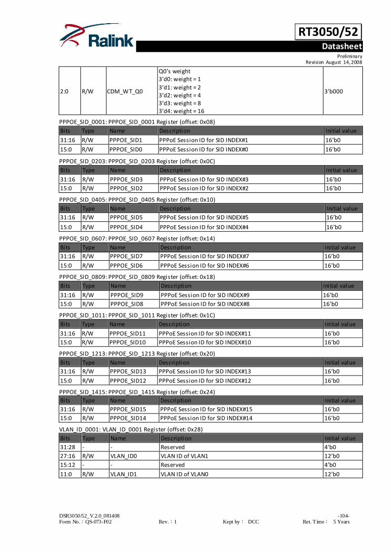
RT3050/52 Datasheet
Preliminary Revision August 14, 2008
DSR3050/52_V.2.0_081408 -104- Form No.:QS-073-F02 Rev.:1 Kept by: DCC Ret. T ime: 5 Years
2:0 R/W CDM_WT_Q0
Q0’s weight 3’d0: weight = 1
3’d1: weight = 2 3’d2: weight = 4 3’d3: weight = 8 3’d4: weight = 16
3’b000
PPPOE_SID_0001: PPPOE_SID_0001 Register (offset: 0x08)
Bits Type Name Description Initial value
31:16 R/W PPPOE_SID1 PPPoE Session ID for SID INDEX#1 16’b0
15:0 R/W PPPOE_SID0 PPPoE Session ID for SID INDEX#0 16’b0
PPPOE_SID_0203: PPPOE_SID_0203 Register (offset: 0x0C)
Bits Type Name Description Initial value
31:16 R/W PPPOE_SID3 PPPoE Session ID for SID INDEX#3 16’b0
15:0 R/W PPPOE_SID2 PPPoE Session ID for SID INDEX#2 16’b0
PPPOE_SID_0405: PPPOE_SID_0405 Register (offset: 0x10)
Bits Type Name Description Initial value
31:16 R/W PPPOE_SID5 PPPoE Session ID for SID INDEX#5 16’b0
15:0 R/W PPPOE_SID4 PPPoE Session ID for SID INDEX#4 16’b0
PPPOE_SID_0607: PPPOE_SID_0607 Register (offset: 0x14)
Bits Type Name Description Initial value
31:16 R/W PPPOE_SID7 PPPoE Session ID for SID INDEX#7 16’b0
15:0 R/W PPPOE_SID6 PPPoE Session ID for SID INDEX#6 16’b0
PPPOE_SID_0809: PPPOE_SID_0809 Register (offset: 0x18)
Bits Type Name Description Initial value
31:16 R/W PPPOE_SID9 PPPoE Session ID for SID INDEX#9 16’b0
15:0 R/W PPPOE_SID8 PPPoE Session ID for SID INDEX#8 16’b0
PPPOE_SID_1011: PPPOE_SID_1011 Register (offset: 0x1C)
Bits Type Name Description Initial value
31:16 R/W PPPOE_SID11 PPPoE Session ID for SID INDEX#11 16’b0
15:0 R/W PPPOE_SID10 PPPoE Session ID for SID INDEX#10 16’b0
PPPOE_SID_1213: PPPOE_SID_1213 Register (offset: 0x20)
Bits Type Name Description Initial value
31:16 R/W PPPOE_SID13 PPPoE Session ID for SID INDEX#13 16’b0
15:0 R/W PPPOE_SID12 PPPoE Session ID for SID INDEX#12 16’b0
PPPOE_SID_1415: PPPOE_SID_1415 Register (offset: 0x24)
Bits Type Name Description Initial value
31:16 R/W PPPOE_SID15 PPPoE Session ID for SID INDEX#15 16’b0
15:0 R/W PPPOE_SID14 PPPoE Session ID for SID INDEX#14 16’b0
VLAN_ID_0001: VLAN_ID_0001 Register (offset: 0x28)
Bits Type Name Description Initial value
31:28 - - Reserved 4’b0
27:16 R/W VLAN_ID0 VLAN ID of VLAN1 12’b0
15:12 - - Reserved 4’b0
11:0 R/W VLAN_ID1 VLAN ID of VLAN0 12’b0

RT3050/52 Datasheet
Preliminary Revision August 14, 2008
DSR3050/52_V.2.0_081408 -105- Form No.:QS-073-F02 Rev.:1 Kept by: DCC Ret. T ime: 5 Years
VLAN_ID_0203: VLAN_ID_0203 Register (offset: 0x2C)
Bits Type Name Description Initial value
31:28 - - Reserved 4’b0
27:16 R/W VLAN_ID2 VLAN ID of VLAN2 12’b0
15:12 - - Reserved 4’b0
11:0 R/W VLAN_ID3 VLAN ID of VLAN3 12’b0
VLAN_ID_0405: VLAN_ID_0405 Register (offset: 0x30)
Bits Type Name Description Initial value
31:28 - - Reserved 4’b0
27:16 R/W VLAN_ID4 VLAN ID of VLAN4 12’b0
15:12 - - Reserved 4’b0
11:0 R/W VLAN_ID5 VLAN ID of VLAN5 12’b0
VLAN_ID_0607: VLAN_ID_0607 Register (offset: 0x34)
Bits Type Name Description Initial value
31:28 - - Reserved 4’b0
27:16 R/W VLAN_ID6 VLAN ID of VLAN6 12’b0
15:12 - - Reserved 4’b0
11:0 R/W VLAN_ID7 VLAN ID of VLAN7 12’b0
VLAN_ID_0809: VLAN_ID_0809 Register (offset: 0x38)
Bits Type Name Description Initial value
31:28 - - Reserved 4’b0
27:16 R/W VLAN_ID8 VLAN ID of VLAN8 12’b0
15:12 - - Reserved 4’b0
11:0 R/W VLAN_ID9 VLAN ID of VLAN9 12’b0
VLAN_ID_1011: VLAN_ID_1011 Register (offset: 0x3C)
Bits Type Name Description Initial value
31:28 - - Reserved 4’b0
27:16 R/W VLAN_ID10 VLAN ID of VLAN10 12’b0
15:12 - - Reserved 4’b0
11:0 R/W VLAN_ID11 VLAN ID of VLAN11 12’b0
VLAN_ID_1213: VLAN_ID_1213 Register (offset: 0x40)
Bits Type Name Description Initial value
31:28 - - Reserved 4’b0
27:16 R/W VLAN_ID12 VLAN ID of VLAN12 12’b0
15:12 - - Reserved 4’b0
11:0 R/W VLAN_ID13 VLAN ID of VLAN13 12’b0
VLAN_ID_14_15: VLAN_ID_14_15 Register (offset: 0x44)
Bits Type Name Description Initial value
31:28 - - Reserved 4’b0
276 R/W VLAN_ID_14 VLAN ID of VLAN14 12’b0
15:12 - - Reserved 4’b0
110 R/W VLAN_ID_15 VLAN ID of VLAN15 12’b0

RT3050/52 Datasheet
Preliminary Revision August 14, 2008
DSR3050/52_V.2.0_081408 -106- Form No.:QS-073-F02 Rev.:1 Kept by: DCC Ret. T ime: 5 Years
3.17.3.6 Register Description - PDMA (base: 0x1010.0100)
PDMA_GLO_CFG: PDMA_GLO_CFG Register (offset:0x00)
Bits Type Name Description Initial value 31:30 - - Reserved 2’b0
29:16 R/W HDR_SEG_LEN
Specify the header segment size in byte to support RX header/
payload scattering function, when set to a non-zero value.
When set to zero, the header/payload scattering feature is disabled.
14’b0
15:8 - - Reserved 8’b0
7 - - Reserved 1’b0
6 R/W TX_WB_DDONE 0 :Disable TX_DMA writing back DDONE into TXD 1 : Enable TX_DMA writing back DDONE into TXD
1’b1
5:4 R/W PDMA_BT_SIZE
Define the burst size of PDMA 0 : 4 DWORD (16bytes)
1 : 8 DWORD (32 bytes) 2 : 16 DWORD (64 bytes) 3 : Reserved
2’d2
3 RO RX_DMA_BUSY 1 : RX_DMA is busy 0 : RX_DMA is not busy
1’b0
2 R/W RX_DMA_EN
1 : Enable RX_DMA
0 : Disable RX_DMA (when disabled, RX_DMA will finish the current receiving packet, then stop.)
1’b0
1 RO TX_DMA_BUSY 1 : TX_DMA is busy 0 : TX_DMA is not busy
1’b0
0 R/W TX_DMA_EN 1 : Enable TX_DMA 0 : Disable TX_DMA (when disabled, TX_DMA will finish the
current sending packet, then stop.)
1’b0
PDMA_RST_IDX: PDMA_RST_IDX Register (offset:0x04)
Bits Type Name Description Initial value
31:17 - - Reserved 15’b0
16 W1C RST_DRX_IDX0 Write 1 to reset to RX_DRX_IDX0 to 0 1’b0
15:4 - - Reserved 12’b0
3 W1C RST_DTX_IDX3 Write 1 to reset to TX_DTX_IDX3 to 0 1’b0
2 W1C RST_DTX_IDX2 Write 1 to reset to TX_DTX_IDX2 to 0 1’b0
1 W1C RST_DTX_IDX1 Write 1 to reset to TX_DTX_IDX1 to 0 1’b0
0 W1C RST_DTX_IDX0 Write 1 to reset to TX_DTX_IDX0 to 0 1’b0
PDMA_SCH_CFG: PDMA_SCH_CFG Register (offset: 0x08)
Bits Type Name Description Initial value
31:26 - - Reserved 7’b0
25:24 R/W PDM_SCH_MOD
2’b00: WRR 2’b01: Strict Priority, Q3>Q2>Q1>Q0 2’b10: Mixed, Q3>WRR(Q2,Q1,Q0) 2’b11: Reserved
2’b00
23:15 - - Reserved 1’b0
14:12 R/W PDM_WT_Q3
Q1’s weight
3’d0: weight = 1 3’d1: weight = 2 3’d2: weight = 4 3’d3: weight = 8
3’d4: weight = 16
3’b011
11 - - Reserved 1’b0

RT3050/52 Datasheet
Preliminary Revision August 14, 2008
DSR3050/52_V.2.0_081408 -107- Form No.:QS-073-F02 Rev.:1 Kept by: DCC Ret. T ime: 5 Years
10:8 R/W PDM_WT_Q2
Q0’s weight 3’d0: weight = 1
3’d1: weight = 2 3’d2: weight = 4 3’d3: weight = 8 3’d4: weight = 16
3’b010
7 - - Reserved 1’b0
6:4 R/W PDM_WT_Q1
Q1’s weight
3’d0: weight = 1 3’d1: weight = 2 3’d2: weight = 4 3’d3: weight = 8
3’d4: weight = 16
3’b001
3 - - Reserved 1’b0
2:0 R/W PDM_WT_Q0
Q0’s weight 3’d0: weight = 1 3’d1: weight = 2 3’d2: weight = 4
3’d3: weight = 8 3’d4: weight = 16
3’b000
DLY_INT_CFG: DLY_INT_CFG Register (offset: 0x0C)
Bits Type Name Description Initial value
31 RW TXDLY_INT_EN 1: Enable TX delayed interrupt mechanism. 0: Disable TX delayed interrupt mechanism.
1’b0
30:24 RW TXMAX_PINT
Specified Max # of pended interrupts.
When the # of pended interrupts equal or grater than the value specified here or interrupt pending time reach the limit (See bellow), an Final TX_DLY_INT is generated.
Set to 0 will disable this feature
7’b0
23:16 RW TXMAX_PTIME
Specified Max pending time for the internal TX_DONE_INT0 and
TX_DONE_INT1. When the pending time equal or greater TXMAX
_PTIME x 20us or the # of pended TX _DONE_INT0 and TX_DONE_INT1
equal or greater than TXMAX_PINT (see above), an Final TX_DLY
_INT is generated
Set to 0 will disable this feature
8’b0
15 RW RXDLY_INT_EN 1: Enable RX delayed interrupt mechanism.
0: Disable RX delayed interrupt mechanism. 1’b0
14:8 RW RXMAX_PINT
Specified Max # of pended interrupts. When the # of pended interrupts equal or grater than the value specified here or interrupt pending time reach the limit (See bellow), an Final RX_DLY_INT is generated.
Set to 0 will disable this feature
7’b0
7:0 RW RXMAX_PTIME
Specified Max pending time for the internal RX_DONE_INT. When the pending time equal or grater RXMAX_PTIME x 20us or,
the # of pended RX_DONE_INT equal or grater than RXMAX_PCNT (see above), an Final RX_DLY_INT is generated
Set to 0 will disable this feature.
8’b0
TX_BASE_PTR0: TX_BASE_PTR0 Register (offset: 0x10)
Bits Type Name Description Initial value
31:0 R/W TX_BASE_PTR0 Point to the base address of TX_Ring0 (4-DWORD aligned address)
32’b0
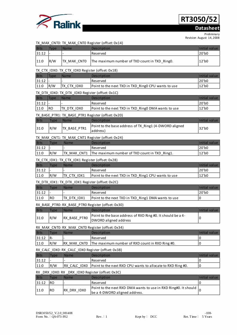
RT3050/52 Datasheet
Preliminary Revision August 14, 2008
DSR3050/52_V.2.0_081408 -108- Form No.:QS-073-F02 Rev.:1 Kept by: DCC Ret. T ime: 5 Years
TX_MAX_CNT0: TX_MAX_CNT0 Register (offset: 0x14)
Bits Type Name Description Initial value
31:12 - - Reserved 20’b0
11:0 R/W TX_MAX_CNT0 The maximum number of TXD count in TXD_Ring0. 12’b0
TX_CTX_IDX0: TX_CTX_IDX0 Register (offset: 0x18)
Bits Type Name Description Initial value
31:12 - - Reserved 20’b0
11:0 R/W TX_CTX_IDX0 Point to the next TXD in TXD_Ring0 CPU wants to use 12’b0
TX_DTX_IDX0: TX_DTX_IDX0 Register (offset: 0x1C)
Bits Type Name Description Initial value
31:12 - - Reserved 20’b0
11:0 RO TX_DTX_IDX0 Point to the next TXD in TXD_Ring0 DMA wants to use 12’b0
TX_BASE_PTR1: TX_BASE_PTR1 Register (offset: 0x20)
Bits Type Name Description Initial value
31:0 R/W TX_BASE_PTR1 Point to the base address of TX_Ring1 (4-DWORD aligned address)
32’b0
TX_MAX_CNT1: TX_MAX_CNT1 Register (offset: 0x24)
Bits Type Name Description Initial value
31:12 - - Reserved 20’b0
11:0 R/W TX_MAX_CNT1 The maximum number of TXD count in TXD_Ring1. 12’b0
TX_CTX_IDX1: TX_CTX_IDX1 Register (offset: 0x28)
Bits Type Name Description Initial value
31:12 - - Reserved 20’b0
11:0 R/W TX_CTX_IDX1 Point to the next TXD in TXD_Ring1 CPU wants to use 12’b0
TX_DTX_IDX1: TX_DTX_IDX1 Register (offset: 0x2C)
Bits Type Name Description Initial value
31:12 - - Reserved 20’b0
11:0 RO TX_DTX_IDX1 Point to the next TXD in TXD_Ring1 DMA wants to use 0
RX_BASE_PTR0: RX_BASE_PTR0 Register (offset: 0x30)
Bits Type Name Description Initial value
31:0 R/W RX_BASE_PTR0 Point to the base address of RXD Ring #0. It should be a 4-DWORD aligned address
0
RX_MAX_CNT0: RX_MAX_CNT0 Register (offset: 0x34)
Bits Type Name Description Initial value
31:12 R- - Reserved 0
11:0 R/W RX_MAX_CNT0 The maximum number of RXD count in RXD Ring #0. 0
RX_CALC_IDX0: RX_CALC_IDX0 Register (offset: 0x38)
Bits Type Name Description Initial value
31:12 - - Reserved 0
11:0 R/W RX_CALC_IDX0 Point to the next RXD CPU wants to allocate to RXD Ring #0. 0
RX _DRX_IDX0: RX _DRX_IDX0 Register (offset: 0x3C)
Bits Type Name Description Initial value
31:12 RO - Reserved 0
11:0 RO RX_DRX_IDX0 Point to the next RXD DMA wants to use in RXD Ring#0. It should be a 4-DWORD aligned address.
0

RT3050/52 Datasheet
Preliminary Revision August 14, 2008
DSR3050/52_V.2.0_081408 -109- Form No.:QS-073-F02 Rev.:1 Kept by: DCC Ret. T ime: 5 Years
TX_BASE_PTR2: TX_BASE_PTR2 Register (offset: 0x40)
Bits Type Name Description Initial value
31:0 R/W TX_BASE_PTR2 Point to the base address of TX_Ring2 (4-DWORD aligned address)
32’b0
TX_MAX_CNT2: TX_MAX_CNT2 Register (offset: 0x44)
Bits Type Name Description Initial value
31:12 - - Reserved 20’b0
11:0 R/W TX_MAX_CNT2 The maximum number of TXD count in TXD_Ring2. 12’b0
TX_CTX_IDX2: TX_CTX_IDX2 Register (offset:0x48)
Bits Type Name Description Initial value
31:12 - - Reserved 20’b0
11:0 R/W TX_CTX_IDX2 Point to the next TXD in TXD_Ring2 CPU wants to use 12’b0
TX_DTX_IDX2: TX_DTX_IDX2 Register (offset: 0x4C)
Bits Type Name Description Initial value
31:12 - - Reserved 20’b0
11:0 RO TX_DTX_IDX2 Point to the next TXD in TXD_Ring2 DMA wants to use 0
TX_BASE_PTR3: TX_BASE_PTR3 Register (offset: 0x50)
Bits Type Name Description Initial value
31:0 R/W TX_BASE_PTR3 Point to the base address of TX_Ring3 (4-DWORD aligned
address) 32’b0
TX_MAX_CNT3: TX_MAX_CNT3 Register (offset: 0x54)
Bits Type Name Description Initial value
31:12 - - Reserved 20’b0
11:0 R/W TX_MAX_CNT3 The maximum number of TXD count in TXD_Ring3. 12’b0
TX_CTX_IDX3: TX_CTX_IDX3 Register (offset: 0x58)
Bits Type Name Description Initial value
31:12 - - Reserved 20’b0
11:0 R/W TX_CTX_IDX3 Point to the next TXD in TXD_Ring3 CPU wants to use 12’b0
TX_DTX_IDX3: TX_DTX_IDX3 Register (offset: 0x5C)
Bits Type Name Description Initial value
31:12 - - Reserved 20’b0
11:0 RO TX_DTX_IDX3 Point to the next TXD in TXD_Ring3 DMA wants to use 0
PDMA_FC_CFG: PDMA_FC_CFG Register (offset: 0xF0)
Bits Type Name Description Initial value
31:30 - - Reserved 2’b0
29:24 R/W PDM_FC_DEF_Q3
Q3 flow control pause condition Bit[5]: pause Q3 when PSE P2 high Q full
Bit[4]: pause Q3 when PSE P2 low Q full Bit[3]: pause Q3 when PSE P1 high Q full Bit[2]: pause Q3 when PSE P1 low Q full
Bit[1]: pause Q3 when PSE P0 high Q full Bit[0]: pause Q3 when PSE P0 low Q ful l
6’b111111
23:22 - - Reserved 2’b0
21:16 R/W PDM_FC_DEF_Q2
Q2 flow control pause condition Bit[5]: pause Q2 when PSE P2 high Q full Bit[4]: pause Q2 when PSE P2 low Q full
Bit[3]: pause Q2 when PSE P1 high Q full Bit[2]: pause Q2 when PSE P1 low Q full Bit[1]: pause Q2 when PSE P0 high Q full
6’b111111

RT3050/52 Datasheet
Preliminary Revision August 14, 2008
DSR3050/52_V.2.0_081408 -110- Form No.:QS-073-F02 Rev.:1 Kept by: DCC Ret. T ime: 5 Years
Bit[0]: pause Q2 when PSE P0 low Q full
15:14 - - Reserved 2’b0
13:8 R/W PDM_FC_DEF_Q1
Q1 flow control pause condition Bit[5]: pause Q1 when PSE P2 high Q full
Bit[4]: pause Q1 when PSE P2 low Q full Bit[3]: pause Q1 when PSE P1 high Q full Bit[2]: pause Q1 when PSE P1 low Q full
Bit[1]: pause Q1 when PSE P0 high Q full Bit[0]: pause Q1 when PSE P0 low Q full
6’b111111
7:6 - - Reserved 2’b0
5:0 R/W PDM_FC_DEF_Q0
Q0 flow control pause condition Bit[5]: pause Q0 when PSE P2 high Q full
Bit[4]: pause Q0 when PSE P2 low Q full Bit[3]: pause Q0 when PSE P1 high Q full Bit[2]: pause Q0 when PSE P1 low Q full Bit[1]: pause Q0 when PSE P0 high Q full
Bit[0]: pause Q0 when PSE P0 low Q full
6’b111111
3.17.3.7 Register Description – Frame Engine Counters (base: 0x1010.0400)
Counter & Meter Table
0x000 PPE_AC_BCNT0 PPE Accounting Group #0 Byte Counter
0x004 PPE_AC_PCNT0 PPE Accounting Group #0 Packet Counter
… …
0x1F8 PPE_AC_BCNT63 PPE Accounting Group #63Byte Counter
0x1FC PPE_AC_PCNT63 PPE Accounting Group #63 Packet Counter
0x200 PPE_MTR_CNT0 -
… -
0x2FC PPE_MTR_CNT63 -
0x300 GDMA_TX_GBCNT0 Transmit good byte count for GDMA port#1&2
0x304 GDMA_TX_GPCNT0 Transmit good pkt count for GDMA port#1&2 (not including flow control frames)
0x308 GDMA_TX_SKIPCNT0 Transmit skip count for GDMA port#1&2
0x30C GDMA_TX_COLCNT0 Transmit collision count for GDMA port#1&2
0x310 – 0x31C
Reserved -
0x320 GDMA_RX_GBCNT0 Received good byte count for GDMA port#1&2
0x324 GDMA_RX_GPCNT0 Received good pkt count for GDMA port#1&2 (not including flow control frames)
0x328 GDMA_RX_OERCNT0 Received overflow error pkt count for GDMA port#1&2
0x32C GDMA_RX_FERCNT0 Received FCS error pkt count for GDMA port#1&2
0x330 GDMA_RX_SERCNT0 Received too short error pkt count for GDMA port#1&2
0x334 GDMA_RX_LERCNT0 Received too long error pkt count for GDMA port#1&2
0x338 GDMA_RX_CERCNT0 Received ip/tcp/udp checksum error pkt count for GDMA port#1&2
0x33C Reserved -

RT3050/52 Datasheet
Preliminary Revision August 14, 2008
DSR3050/52_V.2.0_081408 -111- Form No.:QS-073-F02 Rev.:1 Kept by: DCC Ret. T ime: 5 Years
3.18 Ethernet Switch
3.18.1 Features
Support IEEE 802.3 full duplex flow control
5 10/100Mbps PHY + 1 10/100/1000Mbps RGMII/MII/Reverse MII
Support Spanning Tree port states
Support 1K-MAC address table with direct or XOR hash
QoS
Four priorities queues per port
Packet classification based on incoming port, IEEE 802.1p or IP ToS/DSCP
Strict-Priority Queue (PQ) and Weighted Round Robin (WRR)
VLAN
Port Base VLAN
Double VLAN tagging
802.1q tag VLAN
16 VIDs
MAC address table read and write-able
MAC security – Locking a MAC address to a incoming port
MAC clone support – hash with VID
IGMP support
Broadcast storm prevention

RT3050/52 Datasheet
Preliminary Revision August 14, 2008
DSR3050/52_V.2.0_081408 -112- Form No.:QS-073-F02 Rev.:1 Kept by: DCC Ret. T ime: 5 Years
3.18.2 Block Diagram
DMA
MAC
DMA
MAC
DMA
MAC
DMA
MAC
DMA
MAC
GDMA
GMAC
5 ports FE PHY
P0 P1 P2 P3 P4
Link table
LinkManagement
Data buffer
DataManagement
Address table
AddressManagement
Bridge
GDMA
P6(G1)
Frame Engine
P5(G0)
Fig. 3-18-1 Ethernet Switch Block Diagram

RT3050/52 Datasheet
Preliminary Revision August 14, 2008
DSR3050/52_V.2.0_081408 -113- Form No.:QS-073-F02 Rev.:1 Kept by: DCC Ret. T ime: 5 Years
3.18.3 Register Description (base: 0x1011.0000)
ISR: Interrupt Status Register (offset: 0x00)
Bits Type Name Description Initial value
31:30 RO - Reserved 3’b0
29 RO WATCHDOG1_TMR_EXPIRED
P5 no transmit paqcket alert.
This bit indicating that P5 don’t transmit packet for 3 seconds when P5 need to transmit packet.
1’b0
28 R/W WATCHDOG0_TMR
_EXPIRED
Abnormal Alert
This bit indicating that global queue block counts is less than buf_starvation_th for 3 seconds. Write one clear.
1’b0
27 R/W HAS_INTRUDER Intruder Alert This bit indicating that an unsecured packet is coming into
a secured port. Write one clear.
1’b0
26 R/W PORT_ST_CHG Port status change Any port from link status change. Write one clear.
1’b0
25 R/W BC_STORM
BC storm
The device is undergoing broadcast storm. Write one clear.
1’b0
24 R/W MUST_DROP_LAN
Queue exhausted
The global queue is used up and all packets are dropped. Write one clear.
1’b0
23 R/W GLOBAL_QUE_ FULL
Global Queue Full. Write one clear.
1’b0
22:21 RO - Reserved 2’b0
20 R/W LAN_QUE_FULL[6] Port6 out queue full. Write one clear. 1’b0
19 R/W LAN_QUE_FULL[5] Port5 out queue full. Write one clear. 1’b0
18 R/W LAN_QUE_FULL[4] Port4 out queue full. Write one clear. 1’b0
17 R/W LAN_QUE_FULL[3] Port3 out queue full. Write one clear. 1’b0
16 R/W LAN_QUE_FULL[2] Port2 out queue full. Write one clear. 1’b0
15 R/W LAN_QUE_FULL[1] Port1 out queue full. Write one clear. 1’b0
14 R/W LAN_QUE_FULL[0] Port0 out queue full. Write one clear. 1’b0
13:0 RO - Reserved 14’b0
IMR: Interrupt Mask Register (offset: 0x04)
Bits Type Name Description Initial value
31 RO - Reserved 1’b0
30 R/W SW_INT_MASK_30 Reserved 1’b1
29 R/W SW_INT_MASK_29 Reserved 1’b1
28 R/W SW_INT_MASK_28 Abnormal Alert This bit indicating that global queue block counts is less than buf_starvation_th for 3 seconds. Write one clear.
1’b1
27 R/W SW_INT_MASK_27 Intruder Alert This bit indicating that an unsecured packet is coming into a secured port.
1’b1
26 R/W SW_INT_MASK_26 Port status change Any port from link status change
1’b1
25 R/W SW_INT_MASK_25 BC storm The device is undergoing broadcast storm
1’b1
24 R/W SW_INT_MASK_24 Queue exhausted The global queue is used up and all packets are dropped
1’b1
23 R/W SW_INT_MASK_23 Shared queue full 1’b1
22 R/W SW_INT_MASK_22 Reserved 1’b1

RT3050/52 Datasheet
Preliminary Revision August 14, 2008
DSR3050/52_V.2.0_081408 -114- Form No.:QS-073-F02 Rev.:1 Kept by: DCC Ret. T ime: 5 Years
21 R/W SW_INT_MASK_21 Reserved 1’b1
20 R/W SW_INT_MASK_20 port6 queue full 1’b1
19 R/W SW_INT_MASK_19 port5 queue full 1’b1
18 R/W SW_INT_MASK_18 port4 queue full 1’b1
17 R/W SW_INT_MASK_17 port3 queue full 1’b1
16 R/W SW_INT_MASK_16 port2 queue full 1’b1
15 R/W SW_INT_MASK_15 port1 queue full 1’b1
14 R/W SW_INT_MASK_14 port0 queue full 1’b1
13 R/W SW_INT_MASK_13 Reserved 1’b1
12 R/W SW_INT_MASK_12 Reserved 1’b1
11 R/W SW_INT_MASK_11 Reserved 1’b1
10 R/W SW_INT_MASK_10 Reserved 1’b1
9 R/W SW_INT_MASK_9 Reserved 1’b1
8 R/W SW_INT_MASK_8 Reserved 1’b1
7 R/W SW_INT_MASK_7 Reserved 1’b1
6 R/W SW_INT_MASK_6 Reserved 1’b1
5 R/W SW_INT_MASK_5 Reserved 1’b1
4 R/W SW_INT_MASK_4 Reserved 1’b1
3 R/W SW_INT_MASK_3 Reserved 1’b1
2 R/W SW_INT_MASK_2 Reserved 1’b1
1 R/W SW_INT_MASK_1 Reserved. 1’b1
0 R/W SW_INT_MASK_0 Reserved 1’b1
FCT0: Flow Control Threshold 0 (offset:0x08)
Bits Type Name Description Initial value
31:24 R/W FC_RLS_TH Flow Control Release Threshold Flow control is off when the global queue block counts is greater than the threshold
8’d255
23:16 R/W FC_SET_TH
Flow Control Set Threshold
Flow control will be checked when global queue block counts is less than the threshold
8’d200
15:8 R/W DROP_RLS_TH
Drop Release Threshold
Packets will stop dropping when the global queue block counts is greater than the threshold
8’d110
7:0 R/W DROP_SET_TH
Drop Set Threshold
Packets will start dropping when the global queue block counts is less than the threshold.
8’d90
FCT1: Flow Control Threshold 1 (B + 0C)
Bits Type Name Description Initial value
31:8 RO - Reserved 24’d0
7:0 R/W PORT_TH Per_Port_Th
Per port out queue threshold.
8’d20
PFC0: Priority flow control – 0 (offset: 0x10)
Bits Type Name Description Initial value
31:28 - - Reserved 4’d0
27:24 R/W MTCC_LMT MTCC LIMIT
Back-off count limit. 4’d15
23:16 R/W TURN_OFF_FC Turn off FC When Receiving High Packet Auto-turn-off FC when the programmed ports receive priority packet 0: disable
8’d0

RT3050/52 Datasheet
Preliminary Revision August 14, 2008
DSR3050/52_V.2.0_081408 -115- Form No.:QS-073-F02 Rev.:1 Kept by: DCC Ret. T ime: 5 Years
15:12 R/W VO_NUM
The proportional number of WRR after transmit
exactly the number of packets then proceed to next queue, If equal to 0, force to unlimited mode
4’d0
11:8 R/W CL_NUM The proportional number of WRR after transmit exactly the number of packet then proceed to next
queue.
4’d0
7:4 R/W BE_NUM The proportional number of WRR after transmit exactly the number of packet then proceed to next
queue.
4’d0
3:0 R/W BK_NUM The proportional number of WRR after transmit exactly the number of packet then proceed to next queue.
4’d0
PFC1: Priority Flow control –1 (offset: 0x14)
Bits Type Name Description Initial value
31 R/W P6_USE_Q1_EN Port6 only use q1 enable 1’d0
30:24 R/W EN_TOS[7:0] Port6 ~ port0 TOS_en. 0: disable 7’d0
23:16 R/O EN_VLAN Enable per port VLAN ID and priority check.0: disable. 8’d0
15:14 R/W - Reserved 2’b01
13:12 R/W PORT_PRI6 Port priority By setting this register to force per port’s default priority.
2’b01
11:10 R/W PORT_PRI5 Port priority By setting this register to force per port’s default priority.
2’b01
9:8 R/W PORT_PRI4 Port priority By setting this register to force per port’s default priority.
2’b01
7:6 R/W PORT_PRI3 Port priority
By setting this register to force per port’s default priority. 2’b01
5:4 R/W PORT_PRI2 Port priority By setting this register to force per port’s default priority.
2’b01
3:2 R/W PORT_PRI1 Port priority
By setting this register to force per port’s default priority. 2’b01
1:0 R/W PORT_PRI0 Port priority By setting this register to force per port’s default priority.
2’b01
PFC2: Priority flow control –2 (offset: 0x18)
Bits Type Name Description Initial value
31:24 R/W PRI_TH_VO
Voice Threshold – Highest Priority
The minimum per port out queue can store high packet block count
8’d3
23:16 R/W PRI_TH_CL Control Load Threshold The minimum per port out queue can store low packet
block count
8’d3
15:8 R/W PRI_TH_BE Best Effort threshold The minimum per port out queue can store low packet
block count
8’d3
7:0 R/W PRI_TH_BK Background Threshold – Lowest Priority The minimum per port out queue can store low packet block count
8’d3
GQS0: Global Queue Status – 0 (offset: 0x1C)
Bits Type Name Description Initial value
31:9 RO - Reserved 23’d0
8:0 RO EMPTY_CNT Global Queue Block Counts The number of block count left in queue
9’h16b

RT3050/52 Datasheet
Preliminary Revision August 14, 2008
DSR3050/52_V.2.0_081408 -116- Form No.:QS-073-F02 Rev.:1 Kept by: DCC Ret. T ime: 5 Years
GQS1: Global Queue Status – 1 (offset: 0x20)
Bits Type Name Description Initial value
31:24 RO OUTQUE_FULL_VO Congested Voice Queue The corresponding congested low queue
8’d0
23:16 RO OUTQUE_FULL_CL Congested Control Load Queue
The corresponding congested low queue 8’d0
15:8 RO OUTQUE_FULL_BE Congested Best Effort Queue The corresponding congested low queue
8’d0
7:0 RO OUTQUE_FULL_BK Congested Background Queue The corresponding congested low queue
8’d0
ATS: Address Table Search (offset: 0x24)
Bits Type Name Description Initial value
31:3 RO - Reserved 29’b0
2 RO AT_LKUP_IDLE Address Lookup Idle 1’b0
1 R/W SEARCH_NXT_ ADDR
Search For The Next Address (Self_Clear) 1’b0
0 R/W BEGIN_SEARCH_ ADDR
Start Searching The Address Table (Self_Clear) 1’b0
ATS0: Address Table Status 0 (offset: 0x28)
Bits Type Name Description Initial value
31:22 RO HASH_ADD_LU Address table lookup address 10’d0
21:19 RO - Reserved 3’d0
18:12 RO R_PORT MAP Port map The MAC existing in the bit =1.
7’d0
11 RO - Reserved -
10:7 RO R_VID Member set index 4’d0
6:4 RO R_AGE_FIELD Aging field 3’d0
3 RO - Reserved -
2 RO R_MC_INGRESS MC Ingress 1’b0
1 RO AT_TABLE_END Search to the end of address table 1’b0
0 RO SEARCH_RDY Data is ready (read clear) 1’b0
ATS1: Address Table Status 1 (offset: 0x2C)
Bits Type Name Description Initial value
31:16 - Reserved 16’b0
15:0 RO MAC_AD_SER0 Read MAC address [15:0] 16’bx
ATS2: Address Table Status 2 (offset: 0x30)
Bits Type Name Description Initial value
31:0 RO MAC_AD_SER1 Read MAC address [47:16] 32’b0
WMAD0: WT_MAC_AD0 (offset: 0x34)
Bits Type Name Description Initial value
31:22 RO HASH_ADD_CFG Address table configuration address 10’d0
21:19 RO - Reserved 3’d0
19 RO AT_CFG_IDLE Address table configuration SM idle 1’b1
18:12 R/W W_PORT_MAP Write Port Map Number 7’b0
11 R/W - Reserved
10:7 R/W W_INDEX Write Member Set Index 4’b0
6:4 R/W W_AGE_FIELD Write aging field, 111 : static address, 000 :not used. 001~110:used
3’b0
3 R/W - Reserved
2 R/W W_MC_INGRESS Write Mc_Ingress Bit 1’b0

RT3050/52 Datasheet
Preliminary Revision August 14, 2008
DSR3050/52_V.2.0_081408 -117- Form No.:QS-073-F02 Rev.:1 Kept by: DCC Ret. T ime: 5 Years
1 RO W_MAC_DONE MAC Write Done
1: MAC address write OK, (read_clear) 1’b0
0 R/W W_MAC_CMD MAC Address Write Command 1: the MAC write data is ready and write to MAC table now, self_clear
1’b0
WMAD1: WT_MAC_AD1 (offset: 0x38)
Bits Type Name Description Initial value
31:16 RO - Reserved 16’b0
15:0 R/W W_MAC_15_0 Write MAC address [15:0] 16’h0
WMAD2: WT_MAC_AD2 (offset: 0x3C)
Bits Type Name Description Initial value
31:0 R/W W_MAC_47_16 Write MAC address [47:16] 32’b0
PVIDC0: PVID Configuration 0 (offset: 0x40)
Bits Type Name Description Initial value
31:24 RO - Reserved 8’d0
23:12 R/W P1_PVID Port1 PVID setting 12’d1
11:0 R/W P0_PVID Port0 PVID setting 12’d1
PVIDC1: PVID Configuration 1 (offset: 0x44)
Bits Type Name Description Initial value
31:24 RO - Reserved 8’d0
23:12 R/W P3_PVID Port3 PVID setting 12’d1
11:0 R/W P2_PVID Port2 PVID setting 12’d1
PVIDC2: PVID Configuration 2 (offset: 0x48)
Bits Type Name Description Initial value
31:24 RO - Reserved 8’d0
23:12 R/W P5_PVID Port5 PVID setting 12’d1
11:0 R/W P4_PVID Port4 PVID setting 12’d1
PVIDC3: PVID Configuration 3 (offset: 0x4C)
Bits Type Name Description Initial value
31:12 RO - Reserved 20’d0
11:0 R/W P6_PVID Port6 PVID setting 12’d1
VLANI0: VLAN Identifier 0 (offset: 0x50)
Bits Type Name Description Initial value
31:24 RO - Reserved 8’d0
23:12 R/W VID1 VLAN field Identifier for VLAN 1 12’d2
11:0 R/W VID0 VLAN field Identifier for VLAN 0 12’d1
VLANI1: VLAN Identifier 1 (offset: 0x54)
Bits Type Name Description Initial value
31:24 RO - Reserved 8’d0
23:12 R/W VID3 VLAN field Identifier for VLAN 3 12’d4
11:0 R/W VID2 VLAN field Identifier for VLAN 2 12’d3
VLANI2: VLAN Identifier 2 (offset: 0x58)
Bits Type Name Description Initial value
31:24 RO - Reserved 8’d0
23:12 R/W VID5 VLAN field Identifier for VLAN 5 12’d6
11:0 R/W VID4 VLAN field Identifier for VLAN 4 12’d5
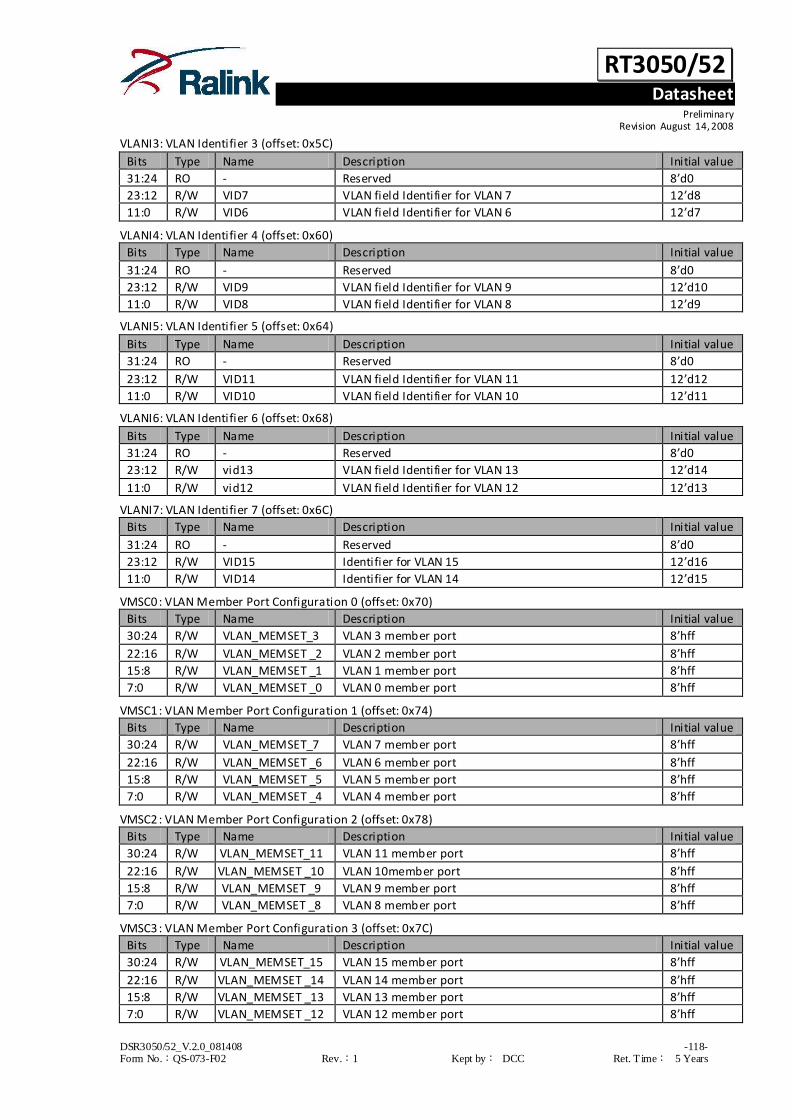
RT3050/52 Datasheet
Preliminary Revision August 14, 2008
DSR3050/52_V.2.0_081408 -118- Form No.:QS-073-F02 Rev.:1 Kept by: DCC Ret. T ime: 5 Years
VLANI3: VLAN Identifier 3 (offset: 0x5C)
Bits Type Name Description Initial value
31:24 RO - Reserved 8’d0
23:12 R/W VID7 VLAN field Identifier for VLAN 7 12’d8
11:0 R/W VID6 VLAN field Identifier for VLAN 6 12’d7
VLANI4: VLAN Identifier 4 (offset: 0x60)
Bits Type Name Description Initial value
31:24 RO - Reserved 8’d0
23:12 R/W VID9 VLAN field Identifier for VLAN 9 12’d10
11:0 R/W VID8 VLAN field Identifier for VLAN 8 12’d9
VLANI5: VLAN Identifier 5 (offset: 0x64)
Bits Type Name Description Initial value
31:24 RO - Reserved 8’d0
23:12 R/W VID11 VLAN field Identifier for VLAN 11 12’d12
11:0 R/W VID10 VLAN field Identifier for VLAN 10 12’d11
VLANI6: VLAN Identifier 6 (offset: 0x68)
Bits Type Name Description Initial value
31:24 RO - Reserved 8’d0
23:12 R/W vid13 VLAN field Identifier for VLAN 13 12’d14
11:0 R/W vid12 VLAN field Identifier for VLAN 12 12’d13
VLANI7: VLAN Identifier 7 (offset: 0x6C)
Bits Type Name Description Initial value
31:24 RO - Reserved 8’d0
23:12 R/W VID15 Identifier for VLAN 15 12’d16
11:0 R/W VID14 Identifier for VLAN 14 12’d15
VMSC0: VLAN Member Port Configuration 0 (offset: 0x70)
Bits Type Name Description Initial value
30:24 R/W VLAN_MEMSET_3 VLAN 3 member port 8’hff
22:16 R/W VLAN_MEMSET _2 VLAN 2 member port 8’hff
15:8 R/W VLAN_MEMSET _1 VLAN 1 member port 8’hff
7:0 R/W VLAN_MEMSET _0 VLAN 0 member port 8’hff
VMSC1: VLAN Member Port Configuration 1 (offset: 0x74)
Bits Type Name Description Initial value
30:24 R/W VLAN_MEMSET_7 VLAN 7 member port 8’hff
22:16 R/W VLAN_MEMSET _6 VLAN 6 member port 8’hff
15:8 R/W VLAN_MEMSET _5 VLAN 5 member port 8’hff
7:0 R/W VLAN_MEMSET _4 VLAN 4 member port 8’hff
VMSC2: VLAN Member Port Configuration 2 (offset: 0x78)
Bits Type Name Description Initial value
30:24 R/W VLAN_MEMSET_11 VLAN 11 member port 8’hff
22:16 R/W VLAN_MEMSET _10 VLAN 10member port 8’hff
15:8 R/W VLAN_MEMSET _9 VLAN 9 member port 8’hff
7:0 R/W VLAN_MEMSET _8 VLAN 8 member port 8’hff
VMSC3: VLAN Member Port Configuration 3 (offset: 0x7C)
Bits Type Name Description Initial value
30:24 R/W VLAN_MEMSET_15 VLAN 15 member port 8’hff
22:16 R/W VLAN_MEMSET _14 VLAN 14 member port 8’hff
15:8 R/W VLAN_MEMSET _13 VLAN 13 member port 8’hff
7:0 R/W VLAN_MEMSET _12 VLAN 12 member port 8’hff

RT3050/52 Datasheet
Preliminary Revision August 14, 2008
DSR3050/52_V.2.0_081408 -119- Form No.:QS-073-F02 Rev.:1 Kept by: DCC Ret. T ime: 5 Years
POA: Port Ability (offset: 0x80)
Bits Type Name Description Initial value
31 RO G1_LINK Port 6 Link 1=up, 0=down
1’b0
30 RO G0_LINK Port 5 Link
1=up, 0=down 1’b0
29:25 RO LINK Port 4 ~ port 0 Link 1=up, 0=down
5’b0
24:23 RO G1_XFC
Flow Control of Port 6 1x = full duplex and tx flow control ON x1= full duplex and rx flow control ON 00 = flow control off
(after AN or forced)
2’b0
22:21 RO G0_XFC
Flow Control of Port 5 1x = full duplex and tx flow control ON x1 = full duplex and rx flow control ON
00 = flow control off (after AN or forced)
2’b0
20:16 RO XFC
Flow Control of PHY port
1 = full duplex and 802.3x flow control ON (after AN or forced)
5’b0
15:9 RO DUPLEX Port6 ~ port0 Duplex, 1= full duplex, 0=half duplex
7’h00
8:7 RO G1_SPD MII port Speed: 10: 1GHz, 01: 100M, 00: 10M
2’b0
6:5 RO G0_SPD MII port Speed:
10: 1GHz, 01: 100M, 00: 10M 2’b0
4:0 RO SPEED Port4 ~ port0 Speed: 1=100M, 0=10M
5’b0
FPA: Force Port4 ~ Port0 Ability (offset: 0x84)
Bits Type Name Description Initial value
31:27 R/W FORCE_MODE Port4 ~ port 0 force mode 5’d0
26:22 R/W FORCE_LNK Port 4 ~ port 0 PHY Link
1=up, 0=down 5’b0
21 RO - Reserved 1’d0
20:16 R/W FORCE_XFC Port 4 ~ port 0 Flow control of PHY port
1 = full duplex and 802.3x flow control ON 5’d0
15:13 RO - Reserved 3’d0
12:8 R/W FORCE_DPX Port4 ~ port0 Duplex, 1= full duplex, 0=half duplex
5’d0
7:5 RO - Reserved 3’d0
4:0 R/W FORCE_SPD Port4 ~ port0 Speed: 1=100M, 0=10M
5’b0
PTS: Port Status (offset: 0x88)
Bits Type Name Description Initial value
31:10 RO - Reserved 22’b0
9 RO G1_TXC_STATUS Port 6 TXC status port 6 TXC status, 1= error, no TXC
1’b0
8 RO G0_TXC_STATUS Port 5 TXC status
port 5 TXC status, 1= error, no TXC 1’b0
7 RO - Reserved 1’b0

RT3050/52 Datasheet
Preliminary Revision August 14, 2008
DSR3050/52_V.2.0_081408 -120- Form No.:QS-073-F02 Rev.:1 Kept by: DCC Ret. T ime: 5 Years
6:0 RO SECURED_ST
Security Status
1= has intruder coming if turn on the SA_secured mode, read clear
7’b0
SOCPC: SoC Port Control (offset: 0x8C)
Bits Type Name Description Initial value
31:26 RO - Reserved 6’b0
25 R/W CRC_PADDING
CRC padding from CPU
If this bit = 1, all packet from CPU will not append CRC and let LAN/WAN port to re-calculate ans attach CRC.
1’b1
24:23 RO - Reserved 2’b0
22:16 R/W DISBC2C PU When this bit = 1, broadcast packets from LAN/WAN
port(s) will not forward to CPU. 7’h7f
15 RO - Reserved 1’b0
14:8 R/W DISMC2C PU When this bit =1, multicast packets from ports will not
forward to CPU. 7’h7f
7 RO - Reserved 1’b0
6:0 R/W DISUN2C PU When this bit is =1 , unknown packets from port(s) will not forward to CPU
7’h7f
POC1: Port Control 0 (offset: 0x90)
Bits Type Name Description Initial value
31:30 R/W HASH_ADDR_SHIFT Address table hashing algorithm option for member set index
2’b0
29 R/W DIS_GMII_PORT_1 Disable port 6 1: port disable (if dumb mode, default = 0)
1’b1
28 R/W DIS_GMII_PORT_0 Disable port 5 1: port disable (if dumb mode, default = 0)
1’b1
27:23 R/W DIS_PORT Disable phy port 1: port disable (if dumb mode, default = 0)
5’h1f
22:16 R/W DISRMC2 CPU 1: disable RMC packet to cpu 7’h0
15 RO - Reserved 1’b0
14:8 R/W EN_FC Enable pause flow control
enable 802.3x flow control 7’h7f
7 RO - Reserved 1’b0
6:0 R/W Reserved Enable back pressure 1: enable back pressure (but need to qualify BP_mode)
7’h7f
POC1: Port Control 1 (offset: 0x94)
Bits Type Name Description Initial value
31:23 RO - Reserved 9’d0
22:16 R/W BLOCKING_STATE 0 : normal state 1 : blocking state, forwarding rmc packet to cpu(need programming address table
7’d0
15 RO - Reserved 1’d0
14:8 R/W DIS_LRNING Disable SA learning 0: enable SA learn
7’b0
7 RO - Reserved 1’d0
6:0 R/W SA_SECURED _PORT
SA secured mode 0: don’t care SA match, 1: the packets’ SA need match, otherwise discard the
packets Note:1. have to set dis_learn and sa_secured at the same
time.
7’b0
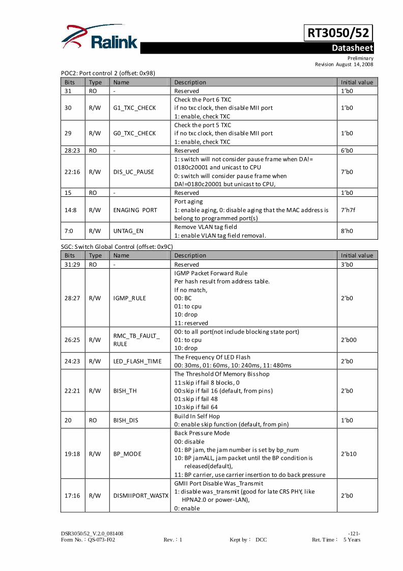
RT3050/52 Datasheet
Preliminary Revision August 14, 2008
DSR3050/52_V.2.0_081408 -121- Form No.:QS-073-F02 Rev.:1 Kept by: DCC Ret. T ime: 5 Years
POC2: Port control 2 (offset: 0x98)
Bits Type Name Description Initial value
31 RO - Reserved 1’b0
30 R/W G1_TXC_CHECK Check the Port 6 TXC if no txc clock, then disable MII port
1: enable, check TXC
1’b0
29 R/W G0_TXC_CHECK Check the port 5 TXC if no txc clock, then disable MII port
1: enable, check TXC
1’b0
28:23 RO - Reserved 6’b0
22:16 R/W DIS_UC_PAUSE
1: switch will not consider pause frame when DA!= 0180c20001 and unicast to CPU
0: switch will consider pause frame when DA!=0180c20001 but unicast to CPU,
7’b0
15 RO - Reserved 1’b0
14:8 R/W ENAGING PORT
Port aging
1: enable aging, 0: disable aging that the MAC address is belong to programmed port(s)
7’h7f
7:0 R/W UNTAG_EN Remove VLAN tag field
1: enable VLAN tag field removal. 8’h0
SGC: Switch Global Control (offset: 0x9C)
Bits Type Name Description Initial value
31:29 RO - Reserved 3’b0
28:27 R/W IGMP_RULE
IGMP Packet Forward Rule Per hash result from address table.
If no match, 00: BC 01: to cpu 10: drop
11: reserved
2’b0
26:25 R/W RMC_TB_FAULT_ RULE
00: to all port(not include blocking state port) 01: to cpu 10: drop
2’b00
24:23 R/W LED_FLASH_TIME The Frequency Of LED Flash 00: 30ms, 01: 60ms, 10: 240ms, 11: 480ms
2’b0
22:21 R/W BISH_TH
The Threshold Of Memory Bisshop
11:skip if fail 8 blocks, 0 00:skip if fail 16 (default, from pins) 01:skip if fail 48 10:skip if fail 64
2’b0
20 RO BISH_DIS Build In Self Hop 0: enable skip function (default, from pin)
1’b0
19:18 R/W BP_MODE
Back Pressure Mode
00: disable 01: BP jam, the jam number is set by bp_num 10: BP jamALL, jam packet until the BP condition is
released(default),
11: BP carrier, use carrier insertion to do back pressure
2’b10
17:16 R/W DISMIIPORT_WASTX
GMII Port Disable Was_Transmit 1: disable was_transmit (good for late CRS PHY, l ike HPNA2.0 or power-LAN),
0: enable
2’b0

RT3050/52 Datasheet
Preliminary Revision August 14, 2008
DSR3050/52_V.2.0_081408 -122- Form No.:QS-073-F02 Rev.:1 Kept by: DCC Ret. T ime: 5 Years
15:12 R/W BP_JAM_CNT
Back Pressure Jam Number
the consecutive jam time when back pressure, default 10 packet jam then one no-jam
4’b1010
11 R/W DISABLE TX BACKOFF Disable The Collision Back Off Timer 1: re-transmit immediately after collision,
1’b0
10:9 R/W ADDRESS_HASH_ALG
MAC Address Hashing Algorithm 00: direct mode, using last 10-bit as hashing address 01: XOR48 mode
10: XOR32 mode, 11:reserved
2’b0
8 R/W DIS_PKT_TX_ABORT 1: Disable collision 16 packet abort and late collision abort 0: enable both abort
1’b1
7:6 R/W PKT_MAX_LEN Maximum Packet Length
00: 1536, 01: 1518, 10: 1522, 11: reserved 2’b0
5:4 R/W BC_STORM_PREV Broadcast Storm Prevention 00: disable , BC will be blocked, if (01: 64 , 10: 48, 11: 32) BC blocks in queue
2’b0
3:0 R/W AGING INTERVAL Aging Timer 0000: disable age, 1xxx: fast age 0001: 300sec, 0010: 600 …… 0111: 38400sec
4’d1
STRT: Switch Reset (offset: 0xA0)
Bits Type Name Description Initial value
31:0 WO Reset_SW Reset switch engine, data, address, link memory , cpu
port and ahb interface when write. 32’b0
LEDP0: LED Port0 (offset: 0xA4)
Bits Type Name Description Initial value
31:4 RO - Reserved 28’d0
3:0 RW P0_LED
port0 LED state, default = link/activity 4’b0000: link
4’b0001: 100M speed 4’b0010: duplex 4’b0011: activity
4’b0100: collision 4’b0101: link/activity 4’b0110: duplex/collsion 4’b0111: 10M speed/activity
4’b1000: 100M speed/activity
4’b0101
LEDP1: LED Port 1 (offset: 0xA8)
Bits Type Name Description Initial value
31:4 RO - Reserved 28’b0
3:0 RW P1_LED Port1 LED state, default = l ink/activity 4’b0101
LEDP2: LED Port2 (offset: 0xAC)
Bits Type Name Description Initial value
31:4 RO - Reserved 28’b0
3:0 RW P2_LED Port2 LED state, default = l ink/activity 4’b0101
LEDP3: LED Port3 (offset: 0xB0)
Bits Type Name Description Initial value
31:4 RO - Reserved 28’b0
3:0 RW P3_LED Port3 LED state, default = l ink/activity 4’b0101

RT3050/52 Datasheet
Preliminary Revision August 14, 2008
DSR3050/52_V.2.0_081408 -123- Form No.:QS-073-F02 Rev.:1 Kept by: DCC Ret. T ime: 5 Years
LEDP4: LED Port4 (offset: 0xB4)
Bits Type Name Description Initial value
31:4 RO - Reserved 28’b0
3:0 RW P4_LED Port4 LED state, default = l ink/activity 4’b0101
WDTR: Watch Dog trigger Reset (offset: 0xB8)
Bits Type Name Description Initial value
31:8 RO - Reserved 24’b0
7:0 RW BUF_STARV_TH Buffer starvation threshold Switch will interrupt CPU when the global queue block counts is less than the threshold for 3 seconds.
8’d30
DES: Debug Signal (offset: 0xBC)
Bits Type Name Description Initial value
31:16 RO - Reserved 16’b0
15:0 RO DEBUG_SIGNAL Port 5 debug signal 16’b0
PCR0: PHY Control Register 0 (offset: 0xC0)
Bits Type Name Description Initial value
31:16 RW WT_NWAY_DATA The data be written into the PHY 17’b0
15 RO - Reserved 1’b0
14 RW RD_PHY_CMD Read command, self_clear 1’b0
13 RW WT_PHY_CMD Write command, self_clear 1’b0
12:8 RW CPU_PHY_REG_ ADDR
PHY register address 5’b0
7:5 RO - Reserved 3’b0
4:0 RW CPU_PHY_ADDR PHY address 5’b0
PCR1: PHY control register 1 (offset: 0xC4)
Bits Type Name Description Initial value
31:16 RO RD_DATA The Read Data 15’b0
15:2 RO - Reserved 14’b0
1 RO RD_RDY Read operation is complete and data is ready, read clear 1’b0
0 RO WT_DONE Write operation is done, read clear 1’b0
FPA : Force Port 5 ~Port 6 ability (offset:0xC8)
Bits Type Name Description Initial value
31:30 RO - Reserved 2’b0
29 R/W AP_EN Port 5 Auto polling enable 1’b0
28:24 R/W EXT_PHY_ADDR_BASE Port 5 External phy base address 5’d5
23:22 R/W G0_RXCLK_SKEW_SEL Port 5 rxclock skew selection 2’d01
21:20 R/W G0_TXCLK_SKEW_SEL Port 5 txclock skew selection 2’d01
19 RO - Reserved 1’d0
18 R/W TURBO_MII_MODE Port 5 turbo MII mode enable 1’b0
17:16 R/O - Reserved 2’b0
15 R/W RGMII_3_3V Port 5 pad 3.3v enable 1’b0
14 R/O - Reserved 1’b0
13 R/W FORCE_RGMII_LINK1 Force port 6 link 1’b0
12 R/W FORCE_ RGMII_LINK0 Force port 5 link 1’b0
11 R/W FORCE_ RGMII_EN1 Force port 6 enable 1’b0
10 R/W FORCE_ RGMII_EN0 Force port 5 enable 1’b0
9:8 R/W FORCE_ RGMII_XFC1 Force port 6 flow control ability 1x: for tx, x1: for rx
2’b11
7:6 R/W FORCE_ RGMII_XFC0 Force port 5 flow control ability 2’b0

RT3050/52 Datasheet
Preliminary Revision August 14, 2008
DSR3050/52_V.2.0_081408 -124- Form No.:QS-073-F02 Rev.:1 Kept by: DCC Ret. T ime: 5 Years
1x: for tx, x1: for rx
5 R/W FORCE_ RGMII_DPX1 Force port 6 duplex 1’b1
4 R/W FORCE_ RGMII_DPX0 Force port 5 duplex 1’b0
3:2 R/W FORCE_ RGMII_SPD1 Force port 6 speed
1x: 1GMhz, 01: 100MHz, 00: 10MHz 2’b10
1:0 R/W FORCE_ RGMII_SPD0 Force port 5 speed 1x: 1GMhz, 01: 100MHz, 00: 10MHz
2’b0
FCT2: Flow Control Threshold 2 (offset: 0xCC)
Bits Type Name Description Initial value
31:18 RO - Reserved 14’d0
17:13 R/W MUST_DROP_RLS_ TH
If the global queue pointer higher than the threshold. The must drop condition will be released.
5’d5
12:8 R/W MUST_DROP_SET_ TH
If the global queue pointer reach must drop. All incoming packets have to be dropped.
5’d3
7:6 RO - Reserved 2’b0
5:0 R/W MC_PER_PORT_TH MC packets per port threshold. 6’d12
QSS0: Queue_Status_0 (offset: 0x D0)
Bits Type Name Description Initial value
31:24 RO - Reserved 8’b0
23:15 RO BE_CNT_R Link control best effort block counter monitor 9’b0
14:5 RO BK_CNT_R Link control background block counter monitor 10’b0
4:0 R/W SEE_CNT_PORT_ SEL
Link control see port counter selection control 5’b0
QSS1: Queue_Status_1 (offset: 0x D4)
Bits Type Name Description Initial value
31:18 RO - Reserved 14’b0
17:9 RO VO_CNT_R Link control best effort block counter monitor 9’b0
8:0 RO CL_CNT_R Link control background block counter monitor 9’b0
DEC: Debug Control (offset: 0x D8)
Bits Type Name Description Initial value
31:24 R/W BRIDGE IPG Bridge IPG byte count 8’d64
23:6 RO - Reserved 18’d0
5:3 R/W DEBUG_SW_PORT_SEL
Port 5 debug selection control 3’b0
2:0 RO - Reserved 3’d0
MTI: Memory Test Information (offset: 0xDC)
Bits Type Name Description Initial value
31:16 RO - Reserved 16’b0
15:7 RO SKIP_BLOCKS Skip block counter 9’bx
6 RO SW_MEM_TEST_ DONE
Switch memory test done 1’bx
5 RO LK_RAM_TEST_
DONE Link ram test done 1’bx
4 RO LK_RAM_TEST_ FAIL
Link ram test fail 1’bx
3 RO AT_RAM_TEST_ DONE
Address table ram test done 1’bx
2 RO AT_RAM_TEST_ FAIL
Address table ram test fail 1’bx
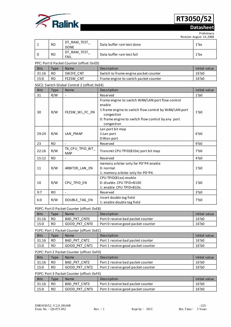
RT3050/52 Datasheet
Preliminary Revision August 14, 2008
DSR3050/52_V.2.0_081408 -125- Form No.:QS-073-F02 Rev.:1 Kept by: DCC Ret. T ime: 5 Years
1 RO DT_RAM_TEST_
DONE Data buffer ram test done 1’bx
0 RO DT_RAM_TEST_ FAIL
Data buffer ram test fail 1’bx
PPC: Port 6 Packet Counter (offset: 0xE0)
Bits Type Name Description Initial value
31:16 RO SW2FE_CNT Switch to frame engine packet counter 16’b0
15:0 RO FE2SW_CNT Frame engine to switch packet counter 16’b0
SGC2: Switch Global Control 2 (offset: 0xE4)
Bits Type Name Description Initial value
31 R/W - Reserved 1’b0
30 R/W FE2SW_WL_FC_EN
Frame engine to switch WAN/LAN port flow control enable
1:frame engine to switch flow control by WAN/LAN port congestion
0: frame engine to switch flow control by any port congestion
1’b0
29:24 R/W LAN_PMAP Lan port bit map 1:Lan port 0:Wan port
6’b0
23 RO - Reserved 9’b0
22:16 R/W TX_CPU_TPID_BIT_ MAP
Transmit CPU TPID(810x) port bit map 7’b0
15:12 RO - Reserved 4’b0
11 R/W ARBITER_LAN_EN memory arbiter only for P0~P4 enable 0: normal 1: memory arbiter only for P0~P4.
1’b0
10 R/W CPU_TPID_EN
CPU TPID(81xx) enable
0: disable. CPU TPID=8100 1: enable. CPU TPID=810x.
1’b0
9:7 RO - Reserved 3’b0
6:0 R/W DOUBLE_TAG_EN Insert double tag field 1: enable double tag field
7’b0
P0PC: Port 0 Packet Counter (offset: 0xE8)
Bits Type Name Description Initial value
31:16 RO BAD_PKT_CNT0 Port 0 receive bad packet counter 16’b0
15:0 RO GOOD_PKT_CNT0 Port 0 receive good packet counter 16’b0
P1PC: Port 1 Packet Counter (offset: 0xEC)
Bits Type Name Description Initial value
31:16 RO BAD_PKT_CNT1 Port 1 receive bad packet counter 16’b0
15:0 RO GOOD_PKT_CNT1 Port 1 receive good packet counter 16’b0
P2PC: Port 2 Packet Counter (offset: 0xF0)
Bits Type Name Description Initial value
31:16 RO BAD_PKT_CNT2 Port 2 receive bad packet counter 16’b0
15:0 RO GOOD_PKT_CNT2 Port 2 receive good packet counter 16’b0
P3PC: Port 3 Packet Counter (offset: 0xF4)
Bits Type Name Description Initial value
31:16 RO BAD_PKT_CNT3 Port 3 receive bad packet counter 16’b0
15:0 RO GOOD_PKT_CNT3 Port 3 receive good packet counter 16’b0

RT3050/52 Datasheet
Preliminary Revision August 14, 2008
DSR3050/52_V.2.0_081408 -126- Form No.:QS-073-F02 Rev.:1 Kept by: DCC Ret. T ime: 5 Years
P4PC: Port 4 packet counter (offset: 0xF8)
Bits Type Name Description Initial value
31:16 RO BAD_PKT_CNT4 Port 4 receive bad packet counter 16’b0
15:0 RO GOOD_PKT_CNT4 Port 4 receive good packet counter 16’b0
P5PC: Port 5 packet counter (offset: 0xFC)
Bits Type Name Description Initial value
31:16 RO BAD_PKT_CNT5 Port 5 receive bad packet counter 16’b0
15:0 RO GOOD_PKT_CNT5 Port 5 receive good packet counter 16’b0
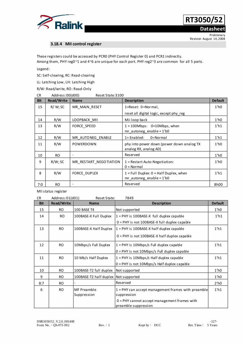
RT3050/52 Datasheet
Preliminary Revision August 14, 2008
DSR3050/52_V.2.0_081408 -127- Form No.:QS-073-F02 Rev.:1 Kept by: DCC Ret. T ime: 5 Years
3.18.4 MII control register
These registers could be accessed by PCR0 (PHY Control Register 0) and PCR1 indirectly.
Among them, PHY reg0~1 and 4~6 are unique for each port. PHY reg2~3 are common for all 5 ports.
Legend:
SC: Self-clearing, RC: Read-clearing
LL: Latching Low, LH: Latching High
R/W: Read/write, RO: Read-Only
CR Address: 00(d00) Reset State:3100
Bit Read/Write Name Description Default
15 R/ W; SC MR_MAIN_RESET 1=Reset: 0=Normal,
reset all digital logic, except phy_reg
1’h0
14 R/W LOOPBACK_MII Mii loop back 1’h0
13 R/W FORCE_SPEED 1 = 100Mbps: 0=10Mbps, when
mr_autoneg_enable = 1’b0
1’h1
12 R/W MR_AUTONEG_ENABLE 1= Enabled: 0=Normal 1’h1
11 R/W POWERDOWN phy into power down (power down analog TX analog RX, analog AD)
1’h0
10 RO - Reserved 1’h0
9 R/W; SC MR_RESTART_NEGOTIATION 1 = Restart Auto-Negotiation: 0 = Normal
1’h0
8 R/W FORCE_DUPLEX 1 = Full Duplex: 0 = Half Duplex, when mr_autoneg_enable = 1’b0
1’h1
7:0 RO - Reserved 8h00
MII status register
CR Address: 01(d01) Reset State: 7849
Bit Read/Write Name Description Default
15 RO 100 BASE T4 Not supported 1’h0
14 RO 100BASE-X Full Duplex 1 = PHY is 100BASE-X full duplex capable
0 = PHY is not 100BASE-X full duplex capable
1’h1
13 RO 100BASE-X Half Duplex 1 = PHY is 100BASE-X half duplex capable
0 = PHY is not 100BASE-X half duplex capable
1’h1
12 RO 10Mbps/s Full Duplex 1 = PHY is 10Mbps/s Full duplex capable
0 = PHY is not 10Mbps/s Full duplex capable
1’h1
11 RO 10 Mb/s Half Duplex 1 = PHY is 10Mbps/s Half duplex capable
0 = PHY is not 10Mbps/s Half duplex capable
1’h1
10 RO 100BASE-T2 full duplex Not supported 1’h0
9 RO 100BASE-T2 half duplex Not supported 1’h0
8:7 RO - Reserved 2’h0
6 RO MF Preamble Suppression
1 = PHY can accept management frames with preamble suppression
0 = PHY cannot accept management frames with preamble suppression
1’h1
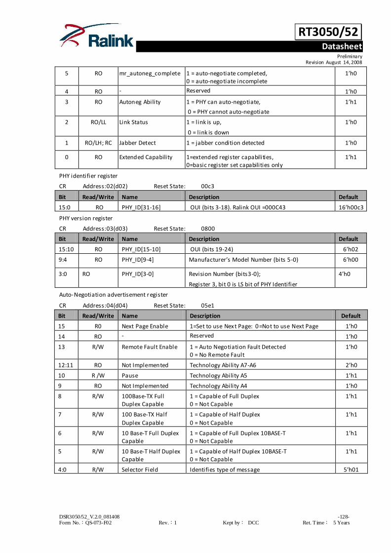
RT3050/52 Datasheet
Preliminary Revision August 14, 2008
DSR3050/52_V.2.0_081408 -128- Form No.:QS-073-F02 Rev.:1 Kept by: DCC Ret. T ime: 5 Years
5 RO mr_autoneg_complete 1 = auto-negotiate completed, 0 = auto-negotiate incomplete
1’h0
4 RO - Reserved 1’h0
3 RO Autoneg Ability 1 = PHY can auto-negotiate,
0 = PHY cannot auto-negotiate
1’h1
2 RO/LL Link Status 1 = l ink is up,
0 = l ink is down
1’h0
1 RO/LH; RC Jabber Detect 1 = jabber condition detected 1’h0
0 RO Extended Capability 1=extended register capabilities, 0=basic register set capabilities only
1’h1
PHY identifier register
CR Address: 02(d02) Reset State: 00c3
Bit Read/Write Name Description Default
15:0 RO PHY_ID[31-16] OUI (bits 3-18). Ralink OUI =000C43 16’h00c3
PHY version register
CR Address: 03(d03) Reset State: 0800
Bit Read/Write Name Description Default
15:10 RO PHY_ID[15-10] OUI (bits 19-24) 6’h02
9:4 RO PHY_ID[9-4] Manufacturer’s Model Number (bits 5-0) 6’h00
3:0 RO PHY_ID[3-0] Revision Number (bits3-0);
Register 3, bit 0 is LS bit of PHY Identifier
4’h0
Auto-Negotiation advertisement register
CR Address: 04(d04) Reset State: 05e1
Bit Read/Write Name Description Default
15 R0 Next Page Enable 1=Set to use Next Page: 0=Not to use Next Page 1’h0
14 RO - Reserved 1’h0
13 R/W Remote Fault Enable 1 = Auto Negotiation Fault Detected 0 = No Remote Fault
1’h0
12:11 RO Not Implemented Technology Ability A7-A6 2’h0
10 R /W Pause Technology Ability A5 1’h1
9 RO Not Implemented Technology Ability A4 1’h0
8 R/W 100Base-TX Full Duplex Capable
1 = Capable of Full Duplex 0 = Not Capable
1’h1
7 R/W 100 Base-TX Half
Duplex Capable
1 = Capable of Half Duplex
0 = Not Capable
1’h1
6 R/W 10 Base-T Full Duplex Capable
1 = Capable of Full Duplex 10BASE-T 0 = Not Capable
1’h1
5 R/W 10 Base-T Half Duplex Capable
1 = Capable of Half Duplex 10BASE-T 0 = Not Capable
1’h1
4:0 R/W Selector Field Identifies type of message 5’h01

RT3050/52 Datasheet
Preliminary Revision August 14, 2008
DSR3050/52_V.2.0_081408 -129- Form No.:QS-073-F02 Rev.:1 Kept by: DCC Ret. T ime: 5 Years
Auto-Negotiation Link partner (LP) ability register
CR Address: 05(d05) Reset State: 0000
Bit Read/Write Name Description Default
15 R O Next Page 1=Link Partner is requesting Next Page function
0=Base Page is requested.
1’h0
14 R O Acknowledge 1= Link partner acknowledge Received Successfully
0 =Not Rec eived
1’h0
13 R O Remote Fault 1 = Auto Negotiation Fault Detected
0 = No Remote Fault
1’h0
12:1
1
R O Not implemented Technology Ability A7-A6 2’h0
10 R O Pause Technology Ability A5 1’h0
9 R O Not Implemented Technology Ability A4 1’h0
8 R O 100Base-TX Full Duplex Capable
1 = Capable
0 = Not Capable
1’h0
7 R O 100 Base-TX Half Duplex Capable
1 = Capable
0 = Not Capable
1’h0
6 R O 10 Base-T Full Duplex Capable
1 = Capable
0 = Not Capable
1’h0
5 R O 10 Base-T Half Duplex
Capable
1 = Capable
0 = Not Capable
1’h0
4:0 RO Selector Field Identifies type of message 5’h00
Auto-Negotiation expansion register
CR Address: 06(d06) Reset State: 0000
Bit R/W/Type Name Description Default
15:5 RO RESERVED No Meaning 11’h0
4 RO/LH; RC Parallel Detection Fault 1 = Local Device Parallel Detection Fault
0 = No fault detected
1’h0
3 RO
Link Partner Next Page
Able
1 = Link Partner is Next Page Able
0 = Link Partner is not Next Page Able
1’h0
2 RO mr_np_able 1 = Local device is Next Page Able
0 = Local device is not Next Page Able
1’h0
1 RO/LH; RC
Page Received 1 = A New Page has been rec eived
0 = A New Page has not been received
1’h0
0 RO
Link Partner Auto-negotiation Able
1 = Link Partner is Auto-negotiation able 0 = Link Partner is not Auto-negotiation able
1’h0

RT3050/52 Datasheet
Preliminary Revision August 14, 2008
DSR3050/52_V.2.0_081408 -130- Form No.:QS-073-F02 Rev.:1 Kept by: DCC Ret. T ime: 5 Years
3.19 USB OTG Controller & PHY
3.19.1 Features
Support USB Host/Device Dual mode
Complies with the On-The-Go Supplement to the USB 2.0 Specification (Revision 1.0a)
Operates in High-Speed (HS, 480-Mbps), Full-Speed (FS, 12-Mbps) and Low-Speed (LS, 1.5-Mbps)
modes
Supports up to 4 bidirectional endpoints, including control endpoint 0
Supports up to 4 host channels.
Supports a generic root hub
Includes automatic ping capabilities
Supports Internal DMA modes
Includes USB power management features
Includes power-saving features (clock gating, two power rails for advanced power management)
Supports packet-based, Dynamic FIFO memory allocation for endpoints for small FIFOs , and flexible,
efficient use of RAM provides support to change an endpointís FIFO memory size during transfers
3.19.2 Block Diagram
Fig. 3-19-1 1.1 USB OTG Controller & PHY Block Diagram

RT3050/52 Datasheet
Preliminary Revision August 14, 2008
DSR3050/52_V.2.0_081408 -131- Form No.:QS-073-F02 Rev.:1 Kept by: DCC Ret. T ime: 5 Years
3.19.3 Register Description (base: 0x101C.0000)
GOTGCTL: OTG Control and Status Register (offset: 0x000)
Bits Type Name Description Mode Initial value
31:20 - - Reserved - 12’h0
19 RO BsesVld
B-Session Valid Indicates the Device mode transceiver status. • 1’b0: B-session is not valid.
• 1’b1: B-session is valid.
In OTG mode, you can use this bit to determine if the
device is connected or disconnected.
Device only
1’b0
18 RO AsesVld
A-Session Valid Indicates the Host mode transceiver status. • 1’b0: A-session is not valid
• 1’b1: A-session is valid
Host
only 1’b0
17 RO DbncTime
Long/Short Debounc e Time
Indicates the debounc e time of a detected connection. • 1’b0: Long debounc e time, used for physical
connections (100 ms + 2.5 μs) •1’b1: Short debounce time, used for soft
connections (2.5 μs)
Host only
1’b0
16 RO ConIDSts
Connector ID Status
Indicates the connector ID status on a connect event. • 1’b0: The DWC_otg core is in A-Device mode
• 1’b1: The DWC_otg core is in B-Device mode
Host and Device
1’b0
15:12 - - Reserved - 4’b0
11 R/W DevHNPEn
Device HNP Enabled The application sets this bit when it successfully receives a SetFeature.SetHNPEnable command from
the connected USB host. • 1’b0: HNP is not enabled in the application
• 1’b1: HNP is enabled in the application
Device only
1’b0
10 R/W HstSetHNPEn
Host Set HNP Enable The application sets this bit when it has successfully enabled HNP (using the SetFeature.SetHNPEnable
command) on the connected device. • 1’b0: Host Set HNP is not enabled
• 1’b1: Host Set HNP is enabled
Host
only
1’b0
9 R/W HNPReq
HNP Request The application sets this bit to initiate an HNP request to the connected USB host. The application can clear this bit by writing a 0 when the Host
Negotiation Success Status Change bit in the OTG Interrupt register (GOTGINT.HstNegSucStsChng) is set. The core clears this bit when the HstNegSucStsChng
bit is cleared. • 1’b0: No HNP request
• 1’b1: HNP request
Device only
1’b0
8 RO HstNegScs Host Negotiation Success The core sets this bit when host negotiation is successful. The
Device only
1’b0
RT3050/52 Datasheet
Preliminary Revision August 14, 2008
DSR3050/52_V.2.0_081408 -132- Form No.:QS-073-F02 Rev.:1 Kept by: DCC Ret. T ime: 5 Years
core clears this bit when the HNP Request (HNPReq)
bit in this register is set. • 1’b0: Host negotiation failure
• 1’b1: Host negotiation success
7:2 - - Reserved - 4’h0
1 R/W SesReq
Session Request The application sets this bit to initiate a session request on the USB.
The application can clear this bit by writing a 0 when the Host Negotiation Success Status Change bit in the OTG Interrupt register (GOTGINT.HstNegSucStsChng)
is set. The core clears this bit when the HstNegSucStsChng bit is cleared. If you use the USB 1.1 Full -Speed Serial Transceiver
interface to initiate the session request, the application must wait until the VBUS discharges to 0.2 V, after the B-Session Valid bit in this register (GOTGCTL.BSesVld) is cleared. This discharge time
varies between different PHYs and can be obtai ned from the PHY vendor. • 1’b0: No session request
• 1’b1: Session request
Device only
1’b0
0 RO SesReqScs
Session Request Success The core sets this bit when a session request
initiation is successful. • 1’b0: Session request failure
• 1’b1: Session request success
Device
only
1’b0
GOTGCTL: OTG Interrupt Register (offset: 0x004)
Bits Type Name Description Mode Initial value
31:20 - - Reserved - 12’h0
19 R_SS_WC
DbnceDone
Debounce Done The core sets this bit when the debounce is completed after the device connect.
The application can start driving USB reset after seeing this interrupt. This bit is only valid when the HNP Capable or SRP Capable bit is set in the Core USB Configuration register (GUSBCFG.HNPCap or
GUSBCFG.SRPCap, respectively).
Host only
1’b0
18 R_SS_WC
ADevTOUTChg A-Device Timeout Change The core sets this bit to indicate that the A-device has timed out while waiting for the B-device to connect.
Host and Device
1’b0
17 R_SS_WC
HstNegDet Host Negotiation Detected The core sets this bit when it detects a host negotiation request on the USB.
Host and Device
1’b0
16:10 - - Reserved - 7’b0
9 R_SS_
WC
HstNegSucSt
sChng
Host Negotiation Success Status Change The core sets this bit on the success or failure of a USB host negotiation request.
The application must read the Host Negotiation Success bit of the OTG Control and Status register (GOTGCTL.HstNegScs) to check for success or failure.
Host
and Device
1’b0

RT3050/52 Datasheet
Preliminary Revision August 14, 2008
DSR3050/52_V.2.0_081408 -133- Form No.:QS-073-F02 Rev.:1 Kept by: DCC Ret. T ime: 5 Years
8 R_SS_WC
SesReqSucStsChng
Session Request Success Status Change
The core sets this bit on the success or failure of a session request. The application must read the Session Request Success bit in the OTG Control and Status register
(GOTGCTL.SesReqScs) to check for success or failure.
Host and Device
1’b0
7:3 - - Reserved - 6’h0
2 R_SS_
WC SesEndDet
Session End Detected
The core sets this bit when the utmiotg_bvalid signal is deasserted.
Host
and Device
1’b0
1:0 - - Reserved - 2’h0
GAHBCFG: Core AHB Configuration Register (offset: 0x008)
Bits Type Name Description Mode Initial value
31:9 - - Reserved - 22’h0
8 R/W PTxFEmpLvl
Periodic TxFIFO Empty Level Indicates when the Periodic TxFIFO Empty Interrupt bit in the Core Interrupt register (GINTSTS.PTxFEmp) is triggered. This bit is used only in Slave mode. • 1’b0: GINTSTS.PTxFEmp interrupt indicates that
the Periodic TxFIFO is half empty • 1’b1: GINTSTS.PTxFEmp interrupt indicates that
the Periodic TxFIFO is completely empty
Host only
1’b0
7 R/W NPTxFEmpLvl
Non-Periodic TxFIFO Empty Level This bit is used only in Slave mode.
In host mode and with Shared FIFO with device mode, this bit indicates when the Non-Periodic TxFIFO Empty Interrupt bit in the Core Interrupt register (GINTSTS. NPTxFEmp) is triggered.
With dedicated FIFO in device mode, this bit indicates when IN endpoint Transmit FIFO empty interrupt (DIEPINTn.TxFEmp) istriggered.
Host mode and with Shared FIFO with device mode: • 1’b0: GINTSTS.NPTxFEmp interrupt indicates that
the Non-Periodic TxFIFO is half empty • 1’b1: GINTSTS.NPTxFEmp interrupt indicates that
the Non-Periodic TxFIFO is completely empty Dedicated FIFO in device mode : • 1’b0: DIEPINTn.TxFEmp interrupt indicates that the
IN Endpoint TxFIFO is half empty • 1’b1: DIEPINTn.TxFEmp interrupt indicates that the
IN Endpoint TxFIFO is completely empty
Host
and Device
1’b0
6 - - Reserved - 1’b0
5 R/W DMAEn
DMA Enable • 1’b0: Core operates in Slave mode
• 1’b1: Core operates in a DMA mode
This bit is always 0 when Slave-Only mode has been selected for the Architecture in coreConsultant (parameter OTG_ARCHITECTURE = 0).
Host
and Device
1’b0

RT3050/52 Datasheet
Preliminary Revision August 14, 2008
DSR3050/52_V.2.0_081408 -134- Form No.:QS-073-F02 Rev.:1 Kept by: DCC Ret. T ime: 5 Years
4:1 R/W HBstLen
Burst Length/Type
This field is used in both External and Internal DMA modes. In External DMA mode, these bits appear on dma_burst[3:0] ports, which can be used by an external wrapper to interface the External DMA
Controller interface to Synopsys DW_ahb_dmac or ARM PrimeCell. External DMA Mode—defines the DMA burst length
in terms of 32-bit words: • 4’b0000: 1 word
• 4’b0001: 4 words
• 4’b0010: 8 words
• 4’b0011: 16 words
• 4’b0100: 32 words
• 4’b0101: 64 words
• 4’b0110: 128 words
• 4’b0111: 256 words
• Others: Reserved
Internal DMA Mode—AHB Master burst type: • 4’b0000 Single
• 4’b0001 INCR
• 4’b0011 INCR4
• 4’b0101 INCR8
• 4’b0111 INCR16
• Others: Reserved
Host
and Device
4’b0
0 R/W GlblIntrMsk
Global Interrupt Mask
The application uses this bit to mask or unmask the interrupt line assertion to itself. Irrespective of this bit’s setting, the interrupt status registers are
updated by the core. •1’b0: Mask the interrupt assertion to the
application. •1’b1: Unmask the interrupt assertion to the
application.
Host
and Device
1’b0
GUSBCFG: Core USB Configuration Register (offset: 0x00C)
Bits Type Name Description Mode Initial value
31 R/W Corrupt Tx packet
Corrupt Tx packet This bit is for debug purposes only. Never set this bit
to 1.
Host and
Device
1’b0
30 R/W ForceDevMode
Force Device Mode Writing a 1 to this bit will force the core to device mode irrespective of utmiotg_iddig input pin. • 1’b0 : Normal Mode.
• 1’b1 : Force Device Mode.
After setting the force bit, the application must wait
at least 25 ms before the change to take effect. When the simulation is in scale down mode, waiting for 500 us is sufficient.
Host and Device
1’b0

RT3050/52 Datasheet
Preliminary Revision August 14, 2008
DSR3050/52_V.2.0_081408 -135- Form No.:QS-073-F02 Rev.:1 Kept by: DCC Ret. T ime: 5 Years
29 R/W ForceHstMode
Writing a 1 to this bit will force the core to host
mode irrespective of utmiotg_iddig input pin. • 1’b0 : Normal Mode.
• 1’b1 : Force Host Mode.
After setting the force bit, the application must wait at least 25 ms before the change to take effect. When the simulation is in scale down mode, waiting for 500 us is sufficient.
Host and
Device
1’b0
28:23 - - Reserved - 6’h0
22 R/W TermSelDLPulse
ULPI External VBUS Indicator This bit indicates to the ULPI PHY to use an external
VBUS over-current indicator. • 1’b0: PHY uses internal VBUS valid comparator.
• 1’b1: PHY uses external VBUS valid comparator.
(Valid only when RTL parameter OTG_HSPHY _INTERFACE = 2 or 3)
Device Only
1’b0
21 R/W ULPIExtVbusIndicator
ULPI External VBUS Indicator This bit indicates to the ULPI PHY to use an external
VBUS over-current indicator. • 1’b0: PHY uses internal VBUS valid comparator.
• 1’b1: PHY uses external VBUS valid comparator.
(Valid only when RTL parameter OTG_ HSPHY_ INTERFACE = 2 or 3)
Host Only
1’b0
20 R/W ULPIExtVbusDrv
ULPI External VBUS Drive This bit selects between internal or external supply
to drive 5V on VBUS, in ULPI PHY. • 1’b0: PHY drives VBUS using internal charge pump
(default). • 1’b1: PHY drives VBUS using external supply.
(Valid only when RTL parameter OTG_ HSPHY_ INTERFACE = 2 or 3)
Host Only
1’b0
19 R/W ULPIClkSusM
ULPI Clock SuspendM This bit sets the ClockSuspendM bit in the Interface Control register on the ULPI PHY. This bit applies only in serial or carkit modes. • 1’b0: PHY powers down internal clock during
suspend. • 1’b1: PHY does not power down internal clock.
(Valid only when RTL parameter OTG_ HSPHY_ INTERFACE = 2 or 3)
Host
and Device
1’b0
18 R/W ULPIAutoRes
ULPI Auto Resume This bit sets the AutoResume bit in the Interface
Control register on the ULPI PHY. • 1’b0: PHY does not use AutoResume feature.
• 1’b1: PHY uses AutoResume feature.
(Valid only when RTL parameter OTG_HSPHY _ INTERFACE = 2 or 3)
Host and Device
1’b0

RT3050/52 Datasheet
Preliminary Revision August 14, 2008
DSR3050/52_V.2.0_081408 -136- Form No.:QS-073-F02 Rev.:1 Kept by: DCC Ret. T ime: 5 Years
17 R/W ULPIFsLs
ULPI FS/LS Selec
The application uses this bit to select the FS/LS serial interface for the ULPI PHY. This bit is valid only when the FS serial transceiver is selected on the ULPI PHY. • 1’b0: ULPI interface
• 1’b1: ULPI FS/LS serial interface
(Valid only when RTL parameters OTG_HSPHY_INTERFACE = 2 or 3 and
OTG_FSPHY_INTERFACE = 1, 2, or 3)
Host
and Device
1’b0
16 RO/R_W
OtgI2CSel
UTMIFS or I C Interface Selec The application uses this bit to select the I2C interface. • 1’b0: UTMI USB 1.1 Full -Speed interface for OTG
signals • 1’b1: I2C interface for OTG signals
This bit is writable only if I2C and UTMIFS were specified for Enable I2C Interface? in coreConsultant (parameter OTG_I2C_INTERFACE = 2). Otherwise,
reads return 0.
Host and
Device
1’b0
15 R/W PhyLPwrClkSel
PHY Low-Power Clock Select Selects either 480-MHz or 48-MHz (low-power) PHY
mode. In FS and LS modes, the PHY can usually operate on a 48-MHz clock to save power. • 1’b0: 480-MHz Internal PLL clock
• 1’b1: 48-MHz External Clock
In 480 MHz mode, the UTMI interface operates at either 60 or 30-MHz, depending upon whether 8- or 16-bit data width is selected. In 48-MHz mode, the
UTMI interface operates at 48 MHz in FS mode and at either 48 or 6 MHz in LS mode (depending on the PHY vendor). This bit drives the utmi_fsls_low_power core output
signal, and is valid only for UTMI+ PHYs.
Host and Device
1’b0
14 - - Reserved - 1’b0
13:10 R/W USBTrdTim
USB Turnaround Time
Sets the turnaround time in PHY clocks. Specifies the response time for a MAC request to the Packet FIFO Controller (PFC) to fetch data from the
DFIFO (SPRAM). This must be programmed to • 4’h5: When the MAC interface is 16-bit UTMI+ .
• 4’h9: When the MAC interface is 8-bit UTMI+ .
Note: The values above are calculated for the minimum AHB fr equency of 30 MHz. USB turnaround time is critical for certification where long cables and
5-Hubs are used, so if you need the AHB to run at less than 30 MHz, and if USB turnaround time is not critical, these bits can be programmed to a larger value. See “Choosing the Value of GUSBCFG.
USBTrdTim” on page 411.
Device
only 4’h5

RT3050/52 Datasheet
Preliminary Revision August 14, 2008
DSR3050/52_V.2.0_081408 -137- Form No.:QS-073-F02 Rev.:1 Kept by: DCC Ret. T ime: 5 Years
9 RO/R
_W HNPCap
HNP-Capable
The application uses this bit to control the DWC_otg core’s HNP capabilities. • 1’b0: HNP capability is not enabled.
• 1’b1: HNP capability is enabled.
This bit is writable only if an HNP mode was specified for Mode of Operation in coreConsultant (parameter OTG_MODE). Otherwise, reads return 0.
Host and
Device
1’b0
8 RO/R_W
SRPCap
SRP-Capable The application uses this bit to control the DWC_otg core SRP capabilities. If the core operates as a non-SRP-capable B-device, it cannot request the
connected A-device (host) to activate VBUS and start a session. • 1’b0: SRP capability is not enabled.
• 1’b1: SRP capability is enabled.
This bit is writable only if an SRP mode was specified for Mode of Operation in coreConsultant (parameter OTG_MODE). Otherwise, reads return 0.
Host and Device
1’b0
7 R/W DDRSel
ULPI DDR Select The application uses this bit to select a Single Data Rate (SDR) or Double Data Rate (DDR) or ULPI interface. • 1’b0: Single Data Rate ULPI Interface, with 8-bit-
wide data bus • 1’b1: Double Data Rate ULPI Interface, with 4-bit-
wide data bus
Host
and Device
1’b0
6 WO/R_W
PHYSel
USB 2.0 High-Speed PHY or USB 1 .1 Full-Speed Serial Transceiver Select The application uses this bit to select either a high-
speed UTMI+ or ULPI PHY, or a full -speed transceiver. • 1’b0: USB 2.0 high-speed UTMI+ or ULPI PHY
• 1’b1: USB 1.1 full -speed serial transceiver
If a USB 1.1 Full -Speed Serial Transceiver interface was not selected in coreConsultant (parameter
OTG_FSPHY_INTERFACE = 0), this bit is always 0, with Write Only access. If a high-speed PHY interface was not selected in coreConsultant (parameter OTG_HSPHY_INTERFACE
= 0), this bit is always 1, with Write Only access. If both interface types were selected in coreConsultant (parameters have non-zero values),
the application uses this bit to select which interface is active, and access is Read and Write.
Host and
Device
1’b0

RT3050/52 Datasheet
Preliminary Revision August 14, 2008
DSR3050/52_V.2.0_081408 -138- Form No.:QS-073-F02 Rev.:1 Kept by: DCC Ret. T ime: 5 Years
5 WO/R
_W FSIntf
Full-Speed Serial Interface Select
The application uses this bit to select either a unidirectional or bidirectional USB 1.1 full -speed serial transceiver interface. • 1’b0: 6-pin unidirectional full -speed serial
interface • 1’b1: 3-pin bidirectional full -speed serial interface
If a USB 1.1 Full -Speed Serial Transceiver interface
was not selected in coreConsultant (parameter OTG_FSPHY_INTERFACE = 0), this bit is always 0, with Write Only access.
If a USB 1.1 FS interface was selected in core Consultant (parameter OTG_FSPHY_INTERFACE ! = 0), then the application can set this bit to select between the 3- and 6-pin interfaces, and access is
Read and Write.
Host and
Device
1’b0
4 RO/R
_W
ULPI_UTMI_
Sel
ULPI or UTMI+ Select The application uses this bit to select either a UTMI+ interface or ULPI Interface. • 1’b0: UTMI+ Interface
• 1’b1: ULPI Interface
This bit is writable only if UTMI+ and ULPI was
specified for High-Speed PHY Interface(s) in coreConsultant configuration (parameter OTG_HSPHY_INTERFACE = 3). Otherwise, reads
return either 0 or 1, depending on the interface selected using the OTG_HSPHY_INTERFACE parameter.
Host
and Device
1’b0
3 RO/R_W
PHYIf
PHY Interface
The application uses this bit to configure the core to support a UTMI+ PHY with an 8- or 16-bit interface. When a ULPI PHY is chosen, this must be set to 8-bit mode. • 1’b0: 8 bits
• 1’b1: 16 bits
This bit is writable only if UTMI+ and ULPI were
selected in coreConsultant configuration (parameter OTG_HSPHY_DWIDTH = 3). Otherwise, this bit returns the value for the power-on interface selected
during configuration.
Host and Device
1’b0

RT3050/52 Datasheet
Preliminary Revision August 14, 2008
DSR3050/52_V.2.0_081408 -139- Form No.:QS-073-F02 Rev.:1 Kept by: DCC Ret. T ime: 5 Years
2:0 R/W TOutCal
HS/FS Timeout Calibration
The number of PHY clocks that the application programs in this field is added to the high-speed/full-speed interpacket timeout duration in the core to account for any additional delays introduced by the
PHY. This can be required, because the delay introduced by the PHY in generating the linestate condition can vary from one PHY to another.
The USB standard timeout value for high-speed operation is 736 to 816 (inclusive) bit times. The USB standard timeout value for full -speed operation is 16 to 18 (inclusive) bit times.
The application must program this field based on the speed of enumeration. The number of bit times added per PHY clock are: High-speed operation: • One 30-MHz PHY clock = 16 bit times
• One 60-MHz PHY clock = 8 bit times
Full-speed operation: • One 30-MHz PHY clock = 0.4 bit times
• One 60-MHz PHY clock = 0.2 bit times
• One 48-MHz PHY clock = 0.25 bit times
Host and Device
3’h0
GRSTCTL: Core Reset Register (offset: 0x010)
Bits Type Name Description Mode Initial value
31 R/O AHBIdle AHB Master Idle Indicates that the AHB Master State Machine is in the IDLE condition.
Host and Device
1’b1
30 R/O DMAReq DMA Request Signal Indicates that the DMA request is in progress. Used for debug.
Host and Device
1’b0
29:11 - - Reserved - 19’h0

RT3050/52 Datasheet
Preliminary Revision August 14, 2008
DSR3050/52_V.2.0_081408 -140- Form No.:QS-073-F02 Rev.:1 Kept by: DCC Ret. T ime: 5 Years
10:6 R/W TxFNum
TxFIFO Number
This is the FIFO number that must be flushed using the TxFIFO Flush bit. This field must not be changed until the core clears the TxFIFO Flush bit. • 5’h0:
- Non-periodic TxFIFO flush in Host mode - Non-periodic TxFIFO flush in device mode when in shared FIFO operation
- Tx FIFO 0 flush in device mode when in dedicated FIFO mode
• 5’h1:
- Periodic TxFIFO flush in Host mode - Periodic TxFIFO 1 flush in Device mode when in shared FIFO operation - TXFIFO 1 flush in device mode when in dedicated
FIFO mode • 5’h2:
- Periodic TxFIFO 2 flush in Device mode when in
shared FIFO operation - TXFIFO 2 flush in device mode when in dedicated FIFO mode
... •5’hF:
- Periodic TxFIFO 15 flush in Device mode when in shared FIFO operation
- TXFIFO 15 flush in device mode when in dedicated FIFO mode
• 5’h10: Flush all the transmit FIFOs in device or
host mode.
Host and Device
5’h0
5 R_WS_SC
TxFFlsh
TxFIFO Flush This bit selectively flushes a single or all transmit FIFOs, but cannot do so if the core is in the midst of a
transaction. The application must write this bit only after checking that the core is neither writing to the TxFIFO nor reading from the TxFIFO. Verify using these registers: • Read—NAK Effective Interrupt ensures the core is
not reading from the FIFO •Write—GRSTCTL.AHBIdle ensures the core is
not writing anything to the FIFO. Flushing is normally recommended when FIFOs are reconfigured or when switching between Shared FIFO and Dedicated Transmit FIFO operation. FIFO flushing
is also recommended during device endpoint disable. The application must wait until the core clears this bit before performing any operations. This bit takes eight
clocks to clear, using the slower clock of phy_clk or hclk.
Host and Device
1’b0
RT3050/52 Datasheet
Preliminary Revision August 14, 2008
DSR3050/52_V.2.0_081408 -141- Form No.:QS-073-F02 Rev.:1 Kept by: DCC Ret. T ime: 5 Years
4 R_WS_SC
RxFFlsh
RxFIFO Flush The application can flush the entire RxFIFO using this bit, but must first ensure that the core is not in the
middle of a transaction. The application must only write to this bit after checking that the core is neither reading from the
RxFIFO nor writing to the RxFIFO. The application must wait until the bit is cleared before performing any other operations. This bit requires 8 clocks (slowest of PHY or AHB clock) to
clear.
Host and Device
1’b0
3 R_WS_SC
INTknQFlsh
IN Token Sequence Learning Queue Flush This bit is valid only if OTG_EN_DED_TX_FIFO = 0. The application writes this bit to flush the IN
Token Sequence Learning Queue.
Device only
1’b0
2 R_WS_SC
FrmCntrRst
Host Frame Counter Reset
The application writes this bit to reset the (micro) frame number counter inside the core. When the (micro)frame counter is reset, the subsequent SOF sent out by the core has a (micro)
frame number of 0.
Host only 1’b0
1 R_WS_SC
HSftRst
HClk Soft Reset The application uses this bit to flush the control logic in the AHB Clock domain. Only AHB Clock Domain
pipelines are reset. • FIFOs are not flushed with this bit.
• All state machines in the AHB clock domain are
reset to the Idle state after terminating the transactions on the AHB, following the protocol.
• CSR control bits used by the AHB clock domain
state machines are cleared. • To clear this interrupt, status mask bits that control
the interrupt status and are generated by the
AHB clock domain state machine are cleared. • Because interrupt status bits are not cleared,
the application can get the status of any core events that occurred after it setthis bit.
This is a self-clearing bit that the core clears after all necessary logic is reset in the core. This can take several clocks, depending on the core’s current
state.
Host and Device
1’b0

RT3050/52 Datasheet
Preliminary Revision August 14, 2008
DSR3050/52_V.2.0_081408 -142- Form No.:QS-073-F02 Rev.:1 Kept by: DCC Ret. T ime: 5 Years
0 R_WS
_SC CSftRst
Core Soft Reset
Resets the hclk and phy_clock domains as follows: • Clears the interrupts and all the CSR registers
except the following register bits:
- PCGCCTL.RstPdwnModule - PCGCCTL.GateHclk - PCGCCTL.PwrClmp - PCGCCTL.StopPPhyLPwrClkSelclk
- GUSBCFG.PhyLPwrClkSel - GUSBCFG.DDRSel - GUSBCFG.PHYSel -GUSBCFG.FSIntf
- GUSBCFG.ULPI_UTMI_Sel - GUSBCFG.PHYIf - HCFG.FSLSPclkSel
- DCFG.DevSpd -GGPIO
• All module state machines (except the AHB Slave
Unit) are reset to the IDLE state, and all the
transmit FIFOs and the receive FIFO are flushed. • Any transactions on the AHB Master are
terminated as soon as possible, after
gracefully completing the last data phase of an AHB transfer. Any transactions on the USB are terminated immediately.
The application can write to this bit any time it
wants to reset the core. This is a self-clearing bit and the core clears this bit after all the necessary logic is reset in the core, which can take several clocks,
depending on the current state of the core. Onc e this bit is cleared software must wait at least 3 PHY clocks before doing any access to the PHY domain (synchronization delay). Software must also must
check that bit 31 of this register is 1 (AHB Master is IDLE) before starting any operation.Typically software reset is used during software development and also
when you dynamically change the PHY selection bits in the USB configuration registers listed above. When you change the PHY, the corresponding clock for the PHY is selected and used in the PHY domain. Once a
new clock is selected, the PHY domain has to be reset for proper operation.
Host
and Device
1’b0
GINTSTS: Core Interrupt Register (offset: 0x014)
Bits Type Name Description Mode Initial value
31 R_SS_WC
WkUpInt
Resume/Remote Wakeup Detected Interrupt In Device mode, this interrupt is asserted when a
resume is detected on the USB. In Host mode, this interrupt is asserted when a remote wakeup is detec ted on the USB. For more information on how to use this interrupt,
see “Partial Power-Down and Clock Gating Programming Model” on page 417.
Host and Device
1’b0
30 R_SS_ SessReqInt Session Request/New Session Detected Interrupt Host 1’b0

RT3050/52 Datasheet
Preliminary Revision August 14, 2008
DSR3050/52_V.2.0_081408 -143- Form No.:QS-073-F02 Rev.:1 Kept by: DCC Ret. T ime: 5 Years
WC In Host mode, this interrupt is asserted when a
session request is detected from the device. In Device mode, this interrupt is asserted when the utmiotg_bvalid signal goes high. For more information on how to use this interrupt,
see “Partial Power-Down and Clock Gating Programming Model” on page 417.
and
Device
29 R_SS_
WC DisconnInt
Disconnect Detected Interrupt
Asserted when a device disconnect is detected.
Host
Only 1’b0
28 R_SS_WC
ConIDStsChng Connector ID Status Change The core sets this bit when there is a change in connector ID status.
Host and Device
1’b0
27 - - Reserved - 1’b0
26 RO PTxFEmp
Periodic TxFIFO Empty Asserted when the Periodic Transmit FIFO is either half or completely empty and there is space for at
least one entry to be written in the Periodic Request Queue. The half or completely empty status is determined by the Periodic TxFIFO Empty Level
bit in the Core AHB Configuration register (GAHBCFG.PTxFEmpLvl).
Host only
1’b1
25 RO HChInt
Host Channels Interrupt The core sets this bit to indicate that an interrupt is
pending on one of the channels of the core (in Host mode). The application must read the Host All Channels
Interrupt (HAINT) register to determine the exact number of the channel on which the interrupt occurred, and then read the corresponding Host Channel-n Interrupt (HCINTn) register to determine
the exact cause of the interrupt. The application must clear the appropriate status bit in the HCINTn register to clear this bit.
Host only
1’b0
24 RO PrtInt
Host Port Interrupt
The core sets this bit to indicate a change in port status of one of the DWC_otg core ports in Host mode. The application must read the Host Port
Control and Status (HPRT) register to determine the exact event that caused this interrupt. The application must clear the appropriate status bit in the Host Port Control and Status register to clear
this bit.
Host
only 1’b0
23 - - Reserved - 1’b0
22 R_SS_
WC FetSusp
Data Fetch Suspended This interrupt is valid only in DMA mode. This
interrupt indicates that the core has stopped fetching data for IN endpoints due to the unavailability of TxFIFO space or Request Queue
space. This interrupt is used by the application for an endpoint mismatch algorithm. For example, after detecting an endpoint mismatch,
the application:
Device
only 1’b0

RT3050/52 Datasheet
Preliminary Revision August 14, 2008
DSR3050/52_V.2.0_081408 -144- Form No.:QS-073-F02 Rev.:1 Kept by: DCC Ret. T ime: 5 Years
• Sets a global non-periodic IN NAK handshake
• Disables In endpoints
• Flushes the FIFO
• Determines the token sequenc e from the IN
Token Sequence Learning Queue • Re-enables the endpoints
• Clears the global non-periodic IN NAK handshake
If the global non-periodic IN NAK is cleared, the core has not yet fetched data for the IN endpoint, and the
IN token is received: the core generates an “IN token received when FIFO empty” interrupt. The OTG then sends the host a NAK response. To avoid this scenario, the
application can check the GINTSTS. FetSusp interrupt, which ensures that the FIFO is full before clearing a global NAK handshake.
Alternatively, the application can mask the “IN token received when FIFO empty” interrupt when clearing a global IN NAK handshake.
21 R_SS_
WC incomplP
Incomplete Periodic Transfer
In Host mode, the core sets this interrupt bit when there are incomplete periodic transactions still pending which are scheduled for the current microframe.
Incomplete Isochronous OUT Transfer (incompISOOUT)
The Device mode, the core sets this interrupt to indicate that there is at least one isochronous OUT endpoint on which the transfer is not completed in the current microframe.
This interrupt is asserted along with the End of Periodic Frame Interrupt (EOPF) bit in this register.
Host
only
Device only
1’b0
20 R_SS_WC
incompISOIN
Incomplete Isochronous IN Transfer The core sets this interrupt to indicate that there is
at least one isochronous IN endpoint on which the transfer is not completed in the current microframe. This interrupt is asserted along with the End of
Periodic Frame Interrupt (EOPF) bit in this register
Device only
1’b0
19 RO OEPInt
OUT Endpoints Interrupt The core sets this bit to indicate that an interrupt is pending on one of the OUT endpoints of the core (in
Device mode). The application must read the Device All Endpoints Interrupt (DAINT) register to determine the exact number of the OUT endpoint on which the interrupt
occurred, and then read the corresponding Device OUT Endpoint-n Interrupt (DOEPINTn) register to determine the exact cause of the
interrupt. The application must clear the appropriate status bit in the corresponding DOEPINTn register to clear this bit.
Device
only 1’b0

RT3050/52 Datasheet
Preliminary Revision August 14, 2008
DSR3050/52_V.2.0_081408 -145- Form No.:QS-073-F02 Rev.:1 Kept by: DCC Ret. T ime: 5 Years
18 RO IEPInt
IN Endpoints Interrupt
The core sets this bit to indicate that an interrupt is pending on one of the IN endpoints of the core (in Device mode). The application must read the Device All Endpoints
Interrupt (DAINT) register to determine the exact number of the IN endpoint on which the interrupt occurred, and then read the corresponding
Device IN Endpoint-n Interrupt (DIEPINTn) register to determine the exact cause of the interrupt. The application must clear the appropriate status bit in the corresponding DIEPINTn register to clear this bit.
Device only
1’b0
17 R_SS_
WC EPMis
Endpoint Mismatch Interrupt Note: This interrupt is valid only in shared FIFO operation. Indicates that an IN token has been received for a
non-periodic endpoint, but the data for another endpoint is present in the top of the Non-periodic Transmit FIFO and the IN endpoint mismatch count
programmed by the application has expired.
Device
only 1’b0
16 - - Reserved - 1’b0
15 R_SS_WC
EOPF
End of Periodic Frame Interrupt Indicates that the period specified in the Periodic
Frame Interval field of the Device Configuration register (DCFG.PerFrInt) has
been reached in the current microframe.
Device only
1’b0
14 R_SS_
WC ISOOutDrop
Isochronous OUT Packet Dropped Interrupt The core sets this bit when it fails to write an isochronous OUT packet into the RxFIFO because
the RxFIFO doesn’t have enough space to accommodate a maximum packet size packet for the isochronous OUT endpoint.
Device
only 1’b0
13 R_SS_WC
EnumDone
Enumeration Done
The core sets this bit to indicate that speed enumeration is complete. The application must read the Device Status (DSTS) register to obtain the
enumerated speed.
Device only
1’b0
12 R_SS_WC
USBRst USB Reset The core sets this bit to indicate that a reset is detected on the USB.
Device only
1’b0
11 R_SS_WC
USBSusp
USB Suspend The core sets this bit to indicate that a suspend was detected on the USB. The core enters the Suspended state when there is no activity on the
phy_line_state_i signal for an extended period of time.
Device only
1’b0
10 R_SS_
WC ErlySusp
Early Suspend
The core sets this bit to indicate that an Idle state has been detected on the USB for 3 ms.
Device
only 1’b0
9 R_SS_
WC I2CINT
I2C Interrupt The core sets this interrupt when I2C access is
completed on the
Host and
Device
1’b0

RT3050/52 Datasheet
Preliminary Revision August 14, 2008
DSR3050/52_V.2.0_081408 -146- Form No.:QS-073-F02 Rev.:1 Kept by: DCC Ret. T ime: 5 Years
I2C interface.
This field is used only if the I2C interface was enabled in coreConsultant (parameter OTG_I2C_INTERFACE = 1). Otherwise, reads return 0.
8 R_SS_WC
ULPICKINT
ULPI Carkit Interrupt
This field is used only if the Carkit interface was enabled in coreConsultant (parameter OTG_ULPI_CARKIT = 1).
Otherwise, reads return 0. The core sets this interrupt when a ULPI Carkit interrupt is received. The core’s PHY sets ULPI Carkit interrupt in UART o
Audio mode. I2C Carkit Interrupt (I2CCKINT) This field is used only if the I2C interface was enabled in coreConsultant (parameter OTG_I2C_INTERFACE =
1). Otherwise, reads return 0. The core sets this interrupt when a Carkit interrupt is
received The core’s PHY sets the I2C Carkit interrupt in Audio mode.
Host and Device
1’b0
7 RO GOUTNakEff
Global OUT NAK Effec tive
Indicates that the Set Global OUT NAK bit in the Device Control register (DCTL.SGOUTNak), set by the application, has taken effect in the core. This bit can
be cleared by writing the Clear Global OUT NAK bit in the Device Control register (DCTL.CGOUTNak).
Device only
1’b0
6 RO GINNakEff
Global IN Non-periodic NAK Effec tive Indicates that the Set Global Non-periodic IN NAK bit
in the Device Control register (DCTL.SGNPInNak), set by the application, has taken effect in the core. That is, the core has sampled the Global IN NAK bit set by the application. This bit can be cleared by clearing
the Clear Global Non-periodic IN NAK bit in the Device Control register (DCTL.CGNPInNak). This interrupt does not necessarily mean that a NAK
handshake is sent out on the USB. The STALL bit takes precedence over the NAK bit.
Device
only 1’b0
5 RO NPTxFEmp
Non-periodic TxFIFO Empty This interrupt is valid only when
OTG_EN_DED_TX_FIFO = 0. This interrupt is asserted when the Non-periodic TxFIFO is either half or completely empty, and there is space for at least one entry to be written to the
Non-periodic Transmit Request Queue. The half or completely empty status is determined by the Non-periodic TxFIFO Empty Level bit in the Core AHB
Configuration register (GAHBCFG.NPTxFEmpLvl).
Host and
Device
1’b1
4 RO RxFLvl RxFIFO Non-Empty Indicates that there is at least one packet pending to be read from the RxFIFO.
Host and Device
1’b0
3 R_SS_WC
Sof Start of (micro)Frame In Host mode, the core sets this bit to indicate that
Host and
1’b0

RT3050/52 Datasheet
Preliminary Revision August 14, 2008
DSR3050/52_V.2.0_081408 -147- Form No.:QS-073-F02 Rev.:1 Kept by: DCC Ret. T ime: 5 Years
an SOF (FS),
micro-SOF (HS), or Keep-Alive (LS) is transmitted on the USB. The application must write a 1 to this bit to clear the interrupt.
In Device mode, in the core sets this bit to indicate that an SOF token has been rec eived on the USB. The application can read the Device Status register to
get the current (micro)frame number . This interrupt is seen only when the core is operating at either HS or FS.
Device
2 RO OTGInt
OTG Interrupt
The core sets this bit to indicate an OTG protocol event. The application must read the OTG Interrupt Status (GOTGINT) register to determine the exact event that caused this interrupt.
The application must clear the appropriate status bit in the GOTGINT register to clear this bit.
Host and Device
1’b0
1 R_SS_
WC ModeMis
Mode Mismatch Interrupt
The core sets this bit when the application is trying to access: • A Host mode register, when the core is operating
in Device mode • A Device mode register, when the core is
operating in Host Mode The register access is completed on the AHB with an OKAY
response, but is ignored by the core internally and doesn’t affect the operation of the core.
Host
and Device
1’b0
0 RO CurMod
Current Mode of Operation Indicates the current mode of operation. • 1’b0: Device mode
• 1’b1: Host mode
Host
and Device
1’b0
GINTMSK: Core Interrupt Mask Register (offset: 0x018)
Bits Type Name Description Mode Initial value
31 R/W WkUpIntMsk Resume/Remote Wakeup Detected Interrupt Mask Host and
Device 1’b0
30 R/W SessReqIntM
sk
Session Request/New Session Detected Interrupt
Mask
Host and
Device 1’b0
29 R/W DisconnIntMsk Disconnect Detected Interrupt Mask Host and
Device 1’b0
28 R/W ConIDStsChn
gMsk Connector ID Status Change Mask
Host and
Device 1’b0
27 - - Reserved - 1’b0
26 R/W PTxFEmpMsk Periodic TxFIFO Empty Mask Host
only 1’b0
25 R/W HChIntMsk Host Channels Interrupt Mask Host only
1’b0
24 R/W PrtIntMsk Host Port Interrupt Mask Host
only 1’b0
23 - - Reserved - 1’b0
22 R/W FetSuspMsk Data Fetch Suspended Mask Device
only 1’b0
RT3050/52 Datasheet
Preliminary Revision August 14, 2008
DSR3050/52_V.2.0_081408 -148- Form No.:QS-073-F02 Rev.:1 Kept by: DCC Ret. T ime: 5 Years
21 R/W Incomplpmsk
Incomplete Periodic Transfer Mask
Incomplete Isochronous OUT Transfer Mask (incompISOOUTMsk)
Host
only
Device
only
1’b0
20 R/W Incompisoinmsk
Incomplete Isochronous IN Transfer Mask Device only
1’b0
19 R/W OEPIntMsk OUT Endpoints Interrupt Mask Device
only 1’b0
18 R/W IEPIntMsk IN Endpoints Interrupt Mask Device only
1’b0
17 R/W EPMisMsk Endpoint Mismatch Interrupt Mask Device only
1’b0
16 - - Reserved 1’b0
15 R/W EOPFMsk End of Periodic Frame Interrupt Mask Device
only 1’b0
14 R/W ISOOutDropMsk
Isochronous OUT Packet Dropped Interrupt Mask Device only
1’b0
13 R/W EnumDoneMsk
Enumeration Done Mask Device only
1’b0
12 R/W USBRstMsk USB Reset Mask Device only
1’b0
11 R/W USBSuspMsk USB Suspend Mask Device only
1’b0
10 R/W ErlySuspMsk Early Suspend Mask Device only
1’b0
9 R/W I2CIntMsk I2C Interrupt Mask Host and
Device 1’b0
8 R/W ULPICKINTMsk
I2CCKINTMsk
ULPI Carkit Interrupt Mask
I2C Carkit Interrupt Mask
Host and
Device 1’b0
7 R/W GOUTNakEffMsk
Global OUT NAK Effec tive Mask Device
only 1’b0
6 R/W GINNakEffM
sk Global Non-periodic IN NAK Effec tive Mask
Device
only 1’b0
5 R/W NPTxFEmpMsk
Non-periodic TxFIFO Empty Mask Host and
Device 1’b0
4 R/W RxFLvlMsk Receive FIFO Non-Empty Mask Host and
Device 1’b0
3 R/W SofMsk Start of (micro)Frame Mask Host and
Device 1’b0
2 R/W OTGIntMsk OTG Interrupt Mask Host and
Device 1’b0
1 R/W ModeMisMsk Mode Mismatch Interrupt Mask Host and
Device 1’b0
0 - - Reserved - 1’b0
GRXSTSR/GRXSTSP: Rec eive Status Debug Read/Status Read and Pop Registers (offset: 0x0 18)
Bits Type Name Description Mode Initial value
31:20 Reserved Resume/Remote Wakeup Detected Interrupt Mask - 11’h0
20:17 RO PktSts
Packet Status
Indicates the status of the rec eived packet • 4’b0010: IN data packet received
• 4’b0011: IN transfer completed (triggers an
interrupt)
- 4’b0

RT3050/52 Datasheet
Preliminary Revision August 14, 2008
DSR3050/52_V.2.0_081408 -149- Form No.:QS-073-F02 Rev.:1 Kept by: DCC Ret. T ime: 5 Years
• 4’b0101: Data toggle error (triggers an interrupt)
• 4’b0111: Channel halted (triggers an interrupt)
• Others: Reserved
16:15 R/W DPID
Data PID
Indicates the Data PID of the rec eived packet • 2’b00: DATA0
• 2’b10: DATA1
• 2’b01: DATA2
•2’b11: MDATA
- 2’b0
14:4 RO BCnt
Byte Count
Indicates the byte count of the received IN data packet.
- 11’h0
3:0 RO ChNum Channel Number Indicates the channel number to which the current
received packet belongs.
- 4’h0
GRXSTSR/GRXSTSP: Device Mode Receive Status Debug Read/Status Read and Pop Registers
Bits Type Name Description Mode Initial value
31:25 - - Reserved - 7’h0
24:21 RO FN
Frame Number This is the least significant 4 bits of the (micro)frame
number in which the packet is received on the USB. This field is supported only when isochronous OUT endpoints are supported.
- 4’h0
20:17 RO PktSts
Packet Status Indicates the status of the rec eived packet • 4’b0001: Global OUT NAK (triggers an interrupt)
• 4’b0010: OUT data packet received
• 4’b0011: OUT transfer completed (triggers an
interrupt) • 4’b0100: SETUP transaction completed (triggers
an interrupt) • 4’b0110: SETUP data packet received
• Others: Reserved
- 4’h0
16:15 RO DPID
Data PID Indicates the Data PID of the rec eived OUT data packet • 2’b00: DATA0
• 2’b10: DATA1
• 2’b01: DATA2
•2’b11: MDATA
- 2’b0
16:4 RO BCnt Byte Count Indicates the byte count of the received data packet.
- 11’h0
3:0 RO EPNum Endpoint Number Indicates the endpoint number to which the current received packet belongs.
- 4’h0
GRXFSIZ: Receive FIFO Size Register(offset: 0x024)
Bits Type Name Description Mode Initial value
31:16 - - Reserved - 16’h0
15:0 RO RxFDep
RxFIFO Depth
This value is in terms of 32-bit words. • Minimum value is 16
• Maximum value is 32,768
- User- selected

RT3050/52 Datasheet
Preliminary Revision August 14, 2008
DSR3050/52_V.2.0_081408 -150- Form No.:QS-073-F02 Rev.:1 Kept by: DCC Ret. T ime: 5 Years
The power-on reset value of this register is specified
as the Largest Rx Data FIFO Depth (parameter OTG_ RX_DFIFO_DEPTH) during coreConsultant configuration. If Enable Dynamic FIFO Sizing? was deselected in
coreConsultant (parameter OTG_DFIFO_DYNAMIC = 0), these flops are optimized, and reads return the power-on value.
If Enable Dynamic FIFO Sizing? was selected in coreConsultant (parameter OTG_DFIFO_DYNAMIC = 1), you can write a new value in this field. You can write a new value in this field.
Programmed values must not exceed the power-on value set in coreConsultant.
GNPTXFSIZ: Non-Periodic Transmit FIFO Size Register (offset: 0x028)
Bits Type Name Description Mode Initial value
31:16 RO/R_W
NPTxFDep
Non-periodic TxFIFO Depth For host mode, this field is always valid.
For Device mode, this field is valid only when OTG_EN_DED_TX_FIFO = 0 This value is in terms of 32-bit words. Minimum value is 16
Maximum value is 32,768 The power-on reset value of this register is specified as the Largest Non-periodic Tx Data FIFO Depth
(parameter OTG_TX_NPERIO_DFIFO_DEPTH when OTG_EN_DED_TX_FIFO = 0. parameter OTG_TX_HNPERIO_DFIFO_DEPTH when OTG_EN_DED_TX_FIFO = 1) during coreConsultant
configuration. If Enable Dynamic FIFO Sizing? was deselected in coreConsultant (parameter OTG_DFIFO_DYNAMIC = 0), these flops are optimized, and reads return the
power-on value. If Enable Dynamic FIFO Sizing? was selected in coreConsultant (parameter OTG_DFIFO_DYNAMIC =
1), you can write a new value in this field. Programmed values must not exceed the power-on value set in coreConsultant. IN Endpoint TxFIFO 0 Depth (INEPTxF0Dep)
This field is valid only for Device mode and when OTG_EN_DED_TX_FIFO = 1 This value is in terms of 32-bit words.
Minimum value is 16 Maximum value is 32,768 The power-on reset value of this register is specified as the Largest IN Endpoint FIFO 0 Depth (parameter OTG_TX_DINEP_DFIFO_DEPTH_0) during
coreConsultant configuration. If Enable Dynamic FIFO Sizing? was deselected in coreConsultant (parameter OTG_DFIFO_DYNAMIC = 0), these flops are optimized, and reads return the
power-on value. If Enable Dynamic FIFO Sizing? was selected in coreConsultant (parameter OTG_DFIFO_DYNAMIC =
- User- selected

RT3050/52 Datasheet
Preliminary Revision August 14, 2008
DSR3050/52_V.2.0_081408 -151- Form No.:QS-073-F02 Rev.:1 Kept by: DCC Ret. T ime: 5 Years
1), you can write a new value in this field.
Programmed values must not exceed the power-on value set in coreConsultant.
15:0 RO/R
_W NPTxFStAddr
Non-periodic Transmit RAM Start Address For host mode, this field is always valid.
For Device mode, this field is valid only when OTG_EN_DED_TX_FIFO = 0 This field contains the memory start address for Non-
periodic Transmit FIFO RAM. The power-on reset value of this register is specified as the Largest Rx Data FIFO Depth (parameter OTG_RX_DFIFO_DEPTH) during coreConsultant
configuration. If Enable Dynamic FIFO Sizing? was deselected in coreConsultant (parameter OTG_DFIFO_DYNAMIC = 0), these flops are optimized, and reads return the
power-on value. If Enable Dynamic FIFO Sizing? was selected in coreConsultant (parameter OTG_DFIFO_DYNAMIC =
1), you can write a new value in this field. Programmed values must not exceed the power-on value set in coreConsultant. IN Endpoint FIFO0 Transmit RAM Start Address
(INEPTxF0StAddr) This field is valid only for Device mode and when OTG_EN_DED_TX_FIFO = 1
This field contains the memory start address for IN Endpoint Transmit FIFO# 0. The power-on reset value of this register is specified as the Largest Rx Data FIFO Depth (parameter
OTG_RX_DFIFO_DEPTH) during coreConsultant configuration. OTG_RX_DFIFO_DEPTH If Enable Dynamic FIFO Sizing? was deselected in
coreConsultant (parameter OTG_DFIFO_DYNAMIC = 0), these flops are optimized, and reads return the power-on value.
If Enable Dynamic FIFO Sizing? was selected in coreConsultant (parameter OTG_DFIFO_DYNAMIC = 1), you can write a new value in this field. Programmed values
must not exceed the power-on value set in coreConsultant.
- User-
selected
GNPTXSTS: Non-Periodic Transmit FIFO/Queue Status Register (offset: 0x02C)
Bits Type Name Description Mode Initial value
31 RO - Reserved - 1’b0
30:24 RO NPTxQTop
Top of the Non-periodic Transmit Request Queue Entry in the Non-periodic Tx Request Queue that is currently being processed by the MAC. • Bits [30:27]: Channel/endpoint number
• Bits [26:25]:
- 2’b00: IN/OUT token
- 2’b01: Zero-length transmit packet (device
- 7’h0

RT3050/52 Datasheet
Preliminary Revision August 14, 2008
DSR3050/52_V.2.0_081408 -152- Form No.:QS-073-F02 Rev.:1 Kept by: DCC Ret. T ime: 5 Years
IN/host OUT)
- 2’b10: PING/CSPLIT token - 2’b11: Channel halt command
• Bit [24]: Terminate (last entry for selected
channel/endpoint)
23:16 RO NPTxQSpcAvail
Non-periodic Transmit Request Queue Space Available Indicates the amount of free space available in the
Non-periodic Transmit Request Queue. This queue holds both IN and OUT requests in Host mode. Device mode has only IN requests. • 8’h0: Non -periodic Transmit Request Queue is full
• 8’h1: 1 location available
• 8’h2: 2 locations available
• n: n locations available (0 ≤ n ≤ 8)
• Others: Reserved
- User- selected
15:0 RO NPTxFSpcAvail
Non-periodic TxFIFO Space Avail Indicates the amount of free space available in the Non-periodic TxFIFO. Values are in terms of 32-bit words. • 16’h0: Non-periodic TxFIFO is full
• 16’h1: 1 word available
• 16’h2: 2 words available
• 16’hn: n words available (where 0 ≤ n ≤ 32,768)
• 16’h8000: 32,768 words available
• Others: Reserved
- User- selected
GI2CCTL:I2C Access Register (offset: 0x030)
Bits Type Name Description Mode Initial value
31 R_WS
_SC BsyDne
I2C Busy/Done The application sets this bit to 1’b1 to start a request on the I2C interface. When the transfer is complete, the core deasserts this bit to 1’b0. As long as the bit
is set, indicating that the I2C interface is busy, the application cannot start another request on the interface.
- 1’b0
30 R/W RW
Read/Write Indicator Indicates whether a read or write register transfer must be performed on the interface. Read/write bursting is not supported for registers. • 1’b1: Read
• 1’b0: Write
- 1’b0
29 - - Reserved - 1’b0
28 R/W I2CDatSe0
I2C DatSe0 USB Mode Selects the address of the I2C Slave on the USB 1.1
full-speed serial transceiver that the core uses for OTG signaling. • 2’b00: 7’h2C
• 2’b01: 7’h2D
• 2’b10: 7’h2E
•2’b11: 7’h2F
- 1’b1
27:26 R/W I2CDevAdr I2C Device Address - 2’b0

RT3050/52 Datasheet
Preliminary Revision August 14, 2008
DSR3050/52_V.2.0_081408 -153- Form No.:QS-073-F02 Rev.:1 Kept by: DCC Ret. T ime: 5 Years
Selects the address of the I C Slave on the USB 1.1
full-speed serial transceiver that the core uses for OTG signaling. • 2’b00: 7’h2C
• 2’b01: 7’h2D
• 2’b10: 7’h2E
•2’b11: 7’h2F
25 R/W I2CSuspCtl
I2C Suspend Control Selects how Suspend is connected to a full -speed transceiver in I2C mode. 1’b0: Use the dedicated utmi_suspend_n pin
1’b1: Use an I2C write to program the Suspend bit in the PHY register
- 1’b0
24 RO Ack
I2C ACK
Indicates whether an ACK response was received from the I2C Slave. This bit is valid when BsyDne is cleared by the core, after application has initiated an I2C access. • 1’b0: NAK
• 1’b1: ACK
- 1’b1
23 R/W I2CEn
I2C Enable
Enables the I2C Master to initiate I2C transactions on the I2C interface.
- 1’b0
22:16 R/W Addr
I2C Address This is the 7-bit I2C device address used by software
to access any external I2C Slave, including the I2C Slave on a USB 1.1 OTG full -speed serial transceiver. Software can change this address to access different
I2C Slaves.
- 7’h0
15:8 R/W RegAddr I2C Register Addr This field programs the address of the register to be read from or written to.
- 8’h00
7:0 R/W RWData
I2C Read/Write Data After a register read operation, this field holds the read data for the application. During a write operation, the application can use this register to
program the write data to be written to a register. During writes, this field holds the write data.
- 8’h00
GPVNDCTL: PHY Vendor Control Register (offset: 0x034)
Bits Type Name Description Mode Initial value
31 R_WS
_SC DisUlpiDrvr
Disable ULPI Drivers This field is used only if the Carkit interface was
enabled in coreConsultant (parameter OTG_ULPI_ CARKIT = 1). Otherwise, reads return 0. The application sets this bit when it has finished
processing the ULPI Carkit Interrupt (GINTSTS. ULPICKINT). When set, the DWC_otg core disables drivers for output signals and masks input signal for the ULPI interface. DWC_otg clears this bit before
enabling the ULPI interface.
- 1’b0
30:28 - - Reserved - 3’h0
27 R_SS_WC_
VStsDone VStatus Done The core sets this bit when the vendor control access
- 1’b0
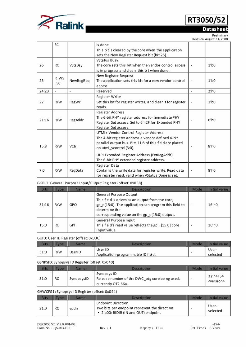
RT3050/52 Datasheet
Preliminary Revision August 14, 2008
DSR3050/52_V.2.0_081408 -154- Form No.:QS-073-F02 Rev.:1 Kept by: DCC Ret. T ime: 5 Years
SC is done.
This bit is cleared by the core when the application sets the New Register Request bit (bit 25).
26 RO VStsBsy VStatus Busy The core sets this bit when the vendor control access
is in progress and clears this bit when done.
- 1’b0
25 R_WS_SC
NewRegReq New Register Request The application sets this bit for a new vendor control
access.
- 1’b0
24:23 - - Reserved - 2’h0
22 R/W RegWr
Register Write
Set this bit for register writes, and clear it for register reads.
- 1’b0
21:16 R/W RegAddr
Register Address
The 6-bit PHY register address for immediate PHY Register Set access. Set to 6’h2F for Extended PHY Register Set access.
- 6’h0
15:8 R/W VCtrl
UTMI+ Vendor Control Register Address
The 4-bit register address a vendor defined 4-bit parallel output bus. Bits 11:8 of this field are placed on utmi_vcontrol[3:0].
ULPI Extended Register Address (ExtRegAddr) The 6-bit PHY extended register address.
- 8’h0
7:0 R/W RegData Register Data Contains the write data for register write. Read data for register read, valid when VStatus Done is set.
- 8’h0
GGPIO: General Purpose Input/Output Register (offset: 0x038)
Bits Type Name Description Mode Initial value
31:16 R/W GPO
General Purpose Output
This field is driven as an output from the core, gp_o[15:0]. The application can program this field to determine the corresponding value on the gp_o[15:0] output.
- 16’h0
15:0 RO GPI General Purpose Input This field’s read value reflects the gp_i*15:0+ core input value.
- 16’h0
GUID: User ID Register (offset: 0x03C)
Bits Type Name Description Mode Initial value
31:0 R/W UserID User ID Application-programmable ID field.
- User- selected
GSNPSID: Synopsys ID Register (offset: 0x040)
Bits Type Name Description Mode Initial value
31:0 RO SynopsysID Synopsys ID Release number of the DWC_otg core being used,
currently OT2.66a.
- 32’h4F54 <version>
GHWCFG1: Synopsys ID Register (offset: 0x044)
Bits Type Name Description Mode Initial value
31:0 RO epdir
Endpoint Direction Two bits per endpoint represent the direction. • 2’b00: BIDIR (IN and OUT) endpoint
- User- selected

RT3050/52 Datasheet
Preliminary Revision August 14, 2008
DSR3050/52_V.2.0_081408 -155- Form No.:QS-073-F02 Rev.:1 Kept by: DCC Ret. T ime: 5 Years
• 2’b01: IN endpoint
• 2’b10: OUT endpoint
•2’b11: Reserved
Bits [31:30]: Endpoint 15 direction
Bits [29:28]: Endpoint 14 direction ... Bits [3:2]: Endpoint 1 direction
Bits[1:0]: Endpoint 0 direction (always BIDIR) (coreConsultant parameter: OTG_EP_DIR_n).
GHWCFG2: User HW Config2 Register (offset: 0x048)
Bits Type Name Description Mode Initial value
31 - - Reserved - 1’b0
30:26 RO TknQDepth
Device Mode IN Token Sequence Learning Queue Depth Range: 0 –30 (coreConsultant parameter:
OTG_TOKEN_QUEUE_DEPTH)
- User- selected
25:24 RO PTxQDepth
Host Mode Periodic Request Queue Depth • 2’b00: 2
• 2’b01: 4
• 2’b10: 8
• Others: Reserved
(coreConsultant parameter: OTG_PERIO_TX_QUEUE_DEPTH)
- User- selected
23:22 RO NPTxQDepth
Non-periodic Request Queue Depth • 2’b00: 2
• 2’b01: 4
• 2’b10: 8
• Others: Reserved
(coreConsultant parameter: OTG_NPERIO_TX_QUEUE_DEPTH)
- User- selected
21:20 - - Reserved - 2’b0
19 RO DynFifoSizing
Dynamic FIFO Sizing Enabled • 1’b0: No
• 1’b1: Yes
(coreConsultant parameter: OTG_DFIFO_DYNAMIC)
- User- selected
18 RO PerioSupport
Periodic OUT Channels Supported in Host Mode • 1’b0: No
• 1’b1: Yes
(coreConsultant parameter: OTG_EN_PERIO_HOST)
- User- selected
17:14 RO NumHstChnl
Number of Host Channels Indicates the number of host channels supported by the core in Host mode. The range of this field is 0–15:
0 specifies 1 channel, 15 specifies 16 channels. (coreConsultant parameter: OTG_NUM_HOST _
CHAN)
- User-
selected
13:10 RO NumDevEps
Number of Device Endpoints
Indicates the number of device endpoints supported by the core in Device mode in addition to control endpoint 0. The range of this field is 1–15. (coreConsultant parameter: OTG_NUM_EPS)
- User- selected

RT3050/52 Datasheet
Preliminary Revision August 14, 2008
DSR3050/52_V.2.0_081408 -156- Form No.:QS-073-F02 Rev.:1 Kept by: DCC Ret. T ime: 5 Years
9:8 RO FSPhyType
Full-Speed PHY Interface Type • 2’b00: Full -speed interface not supported
• 2’b01: Dedicated full -speed interface
• 2’b10: FS pins shared with UTMI+ pins
• 2’b11: FS pins shared with ULPI pins
(coreConsultant parameter: OTG_FSPHY_ INTERFACE)
- User- selected
7:6 RO HSPhyType
High-Speed PHY Interface Type • 2’b00: High-Speed interface not supported
• 2’b01: UTMI+
• 2’b10: ULPI
• 2’b11: UTMI+ and ULPI
(coreConsultant parameter: OTG_HSPHY_
INTERFACE)
- User-
selected
5 RO SingPnt
Point-to-Point • 1’b0: Multi -point application
• 1’b1: Single-point application
(coreConsultant parameter: OTG_SINGLE_ POINT)
- User- selected
4:3 RO OtgArch
Architecture • 2’b00: Slave-Only
• 2’b01: External DMA
• 2’b10: Internal DMA
• Others: Reserved
(coreConsultant parameter:OTG_ ARCHITECTURE )
- User- selected
2:0 RO OtgMode
Mode of Operation • 3’b000: HNP- and SRP-Capable OTG (Host &
Device) • 3’b001: SRP-Capable OTG (Host & Device)
• 3’b010: Non-HNP and Non-SRP Capable OTG
(Host &Device) • 3’b011: SRP-Capable Device
• 3’b100: Non-OTG Device
• 3’b101: SRP-Capable Host
• 3’b110: Non-OTG Host
• Others: Reserved
(coreConsultant parameter: OTG_MODE)
- User- selected
GHWCFG3: User HW Config3 Register (offset: 0x04C)
Bits Type Name Description Mode Initial value
31:16 RO DfifoDepth
DFIFO Depth This value is in terms of 32-bit words. • Minimum value is 32
• Maximum value is 32,768
(coreConsultant parameter: OTG_DFIFO_DEPTH)
- User- Selected
15:12 - - Reserved - 4’b0
11 RO RstType
Reset Style for Clocked always Blocks in RTL • 1’b0: Asynchronous reset is used in the core
• 1’b1: Synchronous reset is used in the core
(coreConsultant parameter: OTG_SYNC_RESET_ TYPE)
- User- selected
10 RO OptFeature Optional Features Removed Indicates whether the User ID register, GPIO
- User- selected

RT3050/52 Datasheet
Preliminary Revision August 14, 2008
DSR3050/52_V.2.0_081408 -157- Form No.:QS-073-F02 Rev.:1 Kept by: DCC Ret. T ime: 5 Years
interface ports, and SOF toggle and counter
ports were removed for gate count optimization by enabling Remove Optional Features? during coreConsultant configuration. • 1’b0: No
• 1’b1: Yes
(coreConsultant parameter: OTG_RM_OPT_FEATURES)
9 RO VndctlSupt
Vendor Control Interface Support • 1’b0: Vendor Control Interface is not available
on the core. • 1’b1: Vendor Control Interface is available.
(coreConsultant parameter: OTG_VENDOR_CTL_ INTERFACE)
- User-
selected
8 RO I2CIntSel
I2C Selection • 1’b0: I2C Interface is not available on the
core. • 1’b1: I2C Interface is available on the core.
(coreConsultant parameter: OTG_I2C_ INTERFACE)
- User- selected
7 RO OtgEn
OTG Function Enabled
The application uses this bit to indicate the DWC_otg core’s OTG capabilities. • 1’b0: Not OTG capable
• 1’b1: OTG Capable
(coreConsultant parameter: OTG_MODE)
- 1’b1
6:4 RO PktSizeWidth
Width of Transfer Size Counters • 4’b0000: 11 bits
• 4’b0001: 12 bits
... • 4’b1000: 19 bits
• Others: Reserved
(coreConsultant parameter: OTG_TRANS_ COUNT_WIDTH)
- User- selected
3:0 RO XferSizeWidth
Width of Transfer Size Counters • 4’b0000: 11 bits
• 4’b0001: 12 bits
... • 4’b1000: 19 bits
• Others: Reserved
(coreConsultant parameter: OTG_TRANS_ COUNT_WIDTH)
- User- selected
GHWCFG4: User HW Config4 Register (offset: 0x050)
Bits Type Name Description Mode Initial value
31:30 - - Reserved - 2’h0
29:26 RO INEps
Number of Device Mode IN Endpoints Including Control Endpoints Range 0 -15 • 0 : 1 IN Endpoint
• 1 : 2 IN Endpoints
• ....
- User Specified

RT3050/52 Datasheet
Preliminary Revision August 14, 2008
DSR3050/52_V.2.0_081408 -158- Form No.:QS-073-F02 Rev.:1 Kept by: DCC Ret. T ime: 5 Years
15 : 16 IN Endpoints
25 RO DedFifoMode
Enable Dedicated Transmit FIFO for device IN Endpoints • 1’b0 : Dedicated Transmit FIFO Operation not
enabled. • 1’b1 : Dedicated Transmit FIFO Operation
enabled.
(coreConsultant parameter : OTG_EN_DED_ TX_FIFO)
- User Selected
24 RO SessEndFltr
“session_end” Filter Enabled
• 1’b0: No fi lter
• 1’b1: Filter
(coreConsultant parameter: OTG_EN_
SESSIONEND_FILTER)
- User-
Selected
23 RO BValidFltr
“b_valid” Filter Enabled
• 1’b0: No fi lter
• 1’b1: Filter
(coreConsultant parameter: OTG_EN_B_VALID_ FILTER)
- User- Selected
22 RO AValidFltr
“a_valid” Filter Enabled
• 1’b0: No fi lter
• 1’b1: Filter
(coreConsultant parameter: OTG_EN_A_VALID_ FILTER)
- User- Selected
21 RO VBusValidFltr
“vbus_valid” Filter Enabled
• 1’b0: No fi lter
• 1’b1: Filter
(coreConsultant parameter: OTG_EN_
VBUSVALID_FILTER)
- User- Selected
20 RO IddgFltr
“iddig” Filter Enable
• 1’b0: No fi lter
• 1’b1: Filter
(coreConsultant parameter: OTG_EN_IDDIG_ FILTER)
- User- Selected
19:16 RO NumCtlEps
Number of Device Mode Control Endpoints in
Addition to Endpoint 0 Range: 0-15 (coreConsultant parameter: OTG_NUM_CRL_
EPS)
- User- Selected
15:14 RO PhyDataWidth
UTMI+ PHY/ULPI-to-Internal UTMI+ Wrapper Data Width When a ULPI PHY is used, an internal wrapper
converts ULPI to UTMI+ . • 2’b00: 8 bits
• 2’b01: 16 bits
• 2’b10: 8/16 bits, software selectable
• Others: Reserved
(coreConsultant parameter: OTG_HSPHY_ DWIDTH)
- User- Selected
13:6 - - Reserved - 8’h0
5 RO AhbFreq Minimum AHB Fr equency Less Than 60 MHz - User-
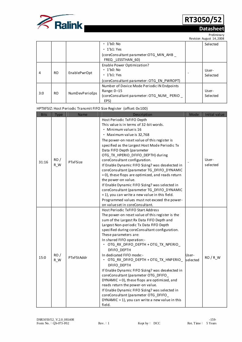
RT3050/52 Datasheet
Preliminary Revision August 14, 2008
DSR3050/52_V.2.0_081408 -159- Form No.:QS-073-F02 Rev.:1 Kept by: DCC Ret. T ime: 5 Years
• 1’b0: No
• 1’b1: Yes
(coreConsultant parameter:OTG_MIN_AHB _ FREQ _LESSTHAN_60)
Selected
4 RO EnablePwrOpt
Enable Power Optimization? • 1’b0: No
• 1’b1: Yes
(coreConsultant parameter: OTG_EN_PWROPT)
- User- Selected
3:0 RO NumDevPerioEps
Number of Device Mode Periodic IN Endpoints Range: 0 –15 (coreConsultant parameter: OTG_NUM_ PERIO _
EPS)
User- Selected
HPTXFSIZ: Host Periodic Transmit FIFO Size Register (offset: 0x100)
Bits Type Name Description Mode Initial value
31:16 RO /
R_W PTxFSize
Host Periodic TxFIFO Depth This value is in terms of 32-bit words. • Minimum value is 16
• Maximum value is 32,768
The power-on reset value of this register is
specified as the Largest Host Mode Periodic Tx Data FIFO Depth (parameter OTG_TX_HPERIO_DFIFO_DEPTH) during coreConsultant configuration.
If Enable Dynamic FIFO Sizing? was deselected in coreConsultant (parameter TG_DFIFO_DYNAMIC = 0), these flops are optimized, and reads return the power-on value.
If Enable Dynamic FIFO Sizing? was selected in coreConsultant (parameter TG_DFIFO_DYNAMIC = 1), you can write a new value in this field.
Programmed values must not exceed the power-on value set in coreConsultant.
- User-
selected
15:0 RO / R_W
PTxFStAddr
Host Periodic TxFIFO Start Address The power-on reset value of this register is the
sum of the Largest Rx Data FIFO Depth and Largest Non-periodic Tx Data FIFO Depth specified during coreConsultant configuration. These parameters are:
In shared FIFO operation:- • OTG_RX_DFIFO_DEPTH + OTG_TX_NPERIO_
DFIFO_DEPTH
In dedicated FIFO mode:- • OTG_RX_DFIFO_DEPTH + OTG_TX_HNPERIO_
DFIFO_DEPTH
If Enable Dynamic FIFO Sizing? was deselected in coreConsultant (parameter OTG_DFIFO_ DYNAMIC = 0), these flops are optimized, and reads return the power-on value.
If Enable Dynamic FIFO Sizing? was selected in coreConsultant (parameter OTG_DFIFO_ DYNAMIC = 1), you can write a new value in this field.
User- selected
RO / R_W

RT3050/52 Datasheet
Preliminary Revision August 14, 2008
DSR3050/52_V.2.0_081408 -160- Form No.:QS-073-F02 Rev.:1 Kept by: DCC Ret. T ime: 5 Years
Programmed values must not exceed the power-
on value set in coreConsultant.
DPTXFSIZn: Device Periodic Transmit FIFO-n Size Register
FIFO_number : 1 ≤ n ≤ 15, (Offset: 104h + (FIFO_number - 1) * 04hh)
Bits Type Name Description Mode Initial value
31:16 RO DPTxFSize
Device Periodic TxFIFO Size
This value is in terms of 32-bit words. • Minimum value is 4
• Maximum value is 768
The value of this register is the Largest Device Mode Periodic Tx Data FIFO Depth (parameter OTG_TX_DPERIO_DFIFO_DEPTH_n), as specified during coreConsultant configuration.
- User-
selected
15:0 RO / R_W
PTxFStAddr
Host Periodic TxFIFO Start Address The power-on reset value of this register is the sum of the Largest Rx Data
FIFO Depth and Largest Non-periodic Tx Data FIFO Depth specified during coreConsultant configuration. These parameters are:
In shared FIFO operation:- • OTG_RX_DFIFO_DEPTH + OTG_TX_NPERIO_
DFIFO_DEPTH
In dedicated FIFO mode:- • OTG_RX_DFIFO_DEPTH + OTG_TX_HNPERIO_
DFIFO_DEPTH If Enable Dynamic FIFO Sizing? was deselected in
coreConsultant (parameter OTG_DFIFO_DYNAMIC = 0), these flops are optimized, and
reads return the power-on value. If Enable Dynamic FIFO Sizing? was selected in coreConsultant (parameter OTG_DFIFO_DYNAMIC = 1), you can write a new
value in this field. Programmed values must not exceed the power-on value set in coreConsultant.
- User- selected
DIEPTXFn: Device IN Endpoint Transmit Fifo Size Register
FIFO_number : 1 ≤ n ≤ 15
(Offset: 104h + (FIFO_number ñ 1) * 04h)
Bits Type Name Description Mode Initial value
31:16 RO / R_W
INEPnTxFDep
IN Endpoint TxFIFO Depth This value is in terms of 32-bit words. Minimum value is 16 Maximum value is 32,768 The power-on reset value of this register is
specified as the Largest IN Endpoint FIFO number Depth (parameter OTG_TX_DINEP_ DFIFO_DEPTH_n) during coreConsultant
configuration (0<n< = 15). If Enable Dynamic FIFO Sizing? was deselected in coreConsultant (parameter OTG_DFIFO_ DYNAMIC = 0), these flops are optimized, and
- User- selected

RT3050/52 Datasheet
Preliminary Revision August 14, 2008
DSR3050/52_V.2.0_081408 -161- Form No.:QS-073-F02 Rev.:1 Kept by: DCC Ret. T ime: 5 Years
reads return the power-on value.
If Enable Dynamic FIFO Sizing? was selected in coreConsultant (parameter OTG_DFIFO_DYNAMIC = 1), you can write a new value in this field. Programmed values must not
exceed the power-on value set in coreConsultant.
15:0 RO / R_W
INEPnTxFStAddr
IN Endpoint FIFOn Transmit RAM Start Address
This field contains the memory start address for IN endpoint Transmit FIFOn (0<n< = 15). The power-on reset value of this register is specified as the Largest Rx Data FIFO Depth
(parameter OTG_RX_DFIFO_DEPTH) during coreConsultant configuration. OTG_RX_DFIFO_DEPTH + SUM 0 to n – 1 (OTG_DINEP_TXFIFO_DEPTH_n)
For example start address of IN endpoint FIFO 1 is OTG_RX_DFIFO_DEPTH + OTG_DINEP_ TXFIFO _DEPTH_0
The start address of IN endpoint FIFO 2 is OTG_RX_DFIFO_DEPTH + OTG_DINEP_TXFIFO _DEPTH_0 + OTG_DINEP_TXFIFO_DEPTH_1 If Enable Dynamic FIFO Sizing? was deselected in
coreConsultant (parameter OTG_DFIFO_DYNAMIC = 0), these flops are optimized, and reads return the power-on value.
If Enable Dynamic FIFO Sizing? was selected in coreConsultant (parameter OTG_DFIFO_DYNAMIC = 1), and you have programmed a new value for RxFIFO depth, you
can write that value in this field. Programmed values must not exceed the power-on value set in coreConsultant.
- User- selected
DIEPTXFn: Device IN Endpoint Transmit Fifo Size Register
FIFO_number : 1 ≤ n ≤ 15
(Offset: 104h + (FIFO_number ñ 1) * 04h)
Bits Type Name Description Mode Initial value
31:16 RO /
R_W INEPnTxFDep
IN Endpoint TxFIFO Depth This value is in terms of 32-bit words. Minimum value is 16 Maximum value is 32,768 The power-on reset value of this register is specified as the
Largest IN Endpoint FIFO number Depth (parameter TG_TX_DINEP_DFIFO_DEPTH_n) during coreConsultant configuration (0<n< = 15). If Enable Dynamic FIFO Sizing? was deselected in
coreConsultant (parameter OTG_DFIFO_ DYNAMIC = 0), these flops are optimized, and reads return the power-on value.
If Enable Dynamic FIFO Sizing? was selected in coreConsultant (parameter OTG_DFIFO_ DYNAMIC = 1), you can write a new value in this field. Programmed values must not exceed the
power-on value set in coreConsultant.
- User-
selected

RT3050/52 Datasheet
Preliminary Revision August 14, 2008
DSR3050/52_V.2.0_081408 -162- Form No.:QS-073-F02 Rev.:1 Kept by: DCC Ret. T ime: 5 Years
15:0 RO / R_W
INEPnTxFStAddr
IN Endpoint FIFOn Transmit RAM Start Address
This field contains the memory start address for IN endpoint Transmit FIFOn (0<n< = 15). The power-on reset value of this register is specified as the Largest Rx Data FIFO Depth
(parameter OTG_RX_DFIFO_DEPTH) during coreConsultant configuration. OTG_RX_DFIFO_DEPTH + SUM 0 to n – 1
(OTG_DINEP_TXFIFO_DEPTH_n) For example start address of IN endpoint FIFO 1 is OTG_RX_DFIFO_DEPTH + OTG_DINEP_TXFIFO_DEPTH_0
The start address of IN endpoint FIFO 2 is OTG_RX_DFIFO_DEPTH + OTG_DINEP_TXFIFO_DEPTH_0 + OTG_DINEP_TXFIFO_DEPTH_1
If Enable Dynamic FIFO Sizing? was deselected in coreConsultant (parameter OTG_DFIFO_ DYNAMIC = 0), these flops are optimized, and
reads return the power-on value. If Enable Dynamic FIFO Sizing? was selected in coreConsultant (parameter OTG_DFIFO_ DYNAMIC= 1), and you have programmed a new
value for RxFIFO depth, you can write that value in this field. Programmed values must not exceed the power-on value set in
coreConsultant.
- User- selected
HCFG: Host Configuration Register (offset: 0x400)
Bits Type Name Description Mode Initial value
31:3 - - Reserved - 30’h0
2 R/W FSLSSupp
FS- and LS-Only Support
The application uses this bit to control the core’s enumeration speed. Using this bit, the application can make the core enumerate as a FS host, even if the connected device supports
HS traffic. Do not make changes to this field after initial programming. • 1’b0: HS/FS/LS, based on the maximum speed
supported by the connected device
• 1’b1: FS/LS-only, even if the connected device can support HS
- 1’b0
1:0 R/W FSLSPclkSel
FS/LS PHY Clock Select
When the core is in FS Host mode • 2’b00: PHY clock is running at 30/60 MHz
• 2’b01: PHY clock is running at 48 MHz
• Others: Reserved
When the core is in LS Host mode • 2’b00: PHY clock is running at 30/60 MHz.
When the UTMI+/ULPI PHY Low Power mode is not selected, use 30/60 MHz. • 2’b01: PHY clock is running at 48 MHz. When
the UTMI+ PHY Low Power mode is selected, use
48MHz if the PHY supplies a 48 MHz clock during
- 2’b0
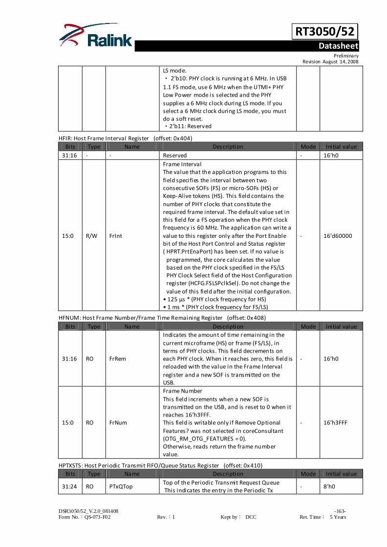
RT3050/52 Datasheet
Preliminary Revision August 14, 2008
DSR3050/52_V.2.0_081408 -163- Form No.:QS-073-F02 Rev.:1 Kept by: DCC Ret. T ime: 5 Years
LS mode. • 2’b10: PHY clock is running at 6 MHz. In USB
1.1 FS mode, use 6 MHz when the UTMI+ PHY Low Power mode is selected and the PHY
supplies a 6 MHz clock during LS mode. If you select a 6 MHz clock during LS mode, you must do a soft reset. •2’b11: Reserved
HFIR: Host Frame Interval Register (offset: 0x404)
Bits Type Name Description Mode Initial value
31:16 - - Reserved - 16’h0
15:0 R/W FrInt
Frame Interval The value that the application programs to this
field specifies the interval between two consecutive SOFs (FS) or micro-SOFs (HS) or Keep-Alive tokens (HS). This field contains the
number of PHY clocks that constitute the required frame interval. The default value set in this field for a FS operation when the PHY clock frequency is 60 MHz. The application can write a
value to this register only after the Port Enable bit of the Host Port Control and Status register ( HPRT.PrtEnaPort) has been set. If no value is
programmed, the core calculates the value based on the PHY clock specified in the FS/LS PHY Clock Select field of the Host Configuration register (HCFG.FSLSPclkSel). Do not change the
value of this field after the initial configuration. • 125 μs * (PHY clock frequency for HS) • 1 ms * (PHY clock frequency for FS/LS)
- 16’d60000
HFNUM: Host Frame Number/Frame Time Remaining Register (offset: 0x408)
Bits Type Name Description Mode Initial value
31:16 RO FrRem
Indicates the amount of time remaining in the
current microframe (HS) or frame (FS/LS), in terms of PHY clocks. This field decrements on each PHY clock. When it reaches zero, this field is reloaded with the value in the Frame Interval
register and a new SOF is transmitted on the USB.
- 16’h0
15:0 RO FrNum
Frame Number
This field increments when a new SOF is transmitted on the USB, and is reset to 0 when it reaches 16’h3FFF. This field is writable only if Remove Optional
Features? was not selected in coreConsultant (OTG_RM_OTG_FEATURES = 0). Otherwise, reads return the frame number value.
- 16’h3FFF
HPTXSTS: Host Periodic Transmit FIFO/Queue Status Register (offset: 0x410)
Bits Type Name Description Mode Initial value
31:24 RO PTxQTop Top of the Periodic Transmit Request Queue This indicates the entry in the Periodic Tx
- 8’h0
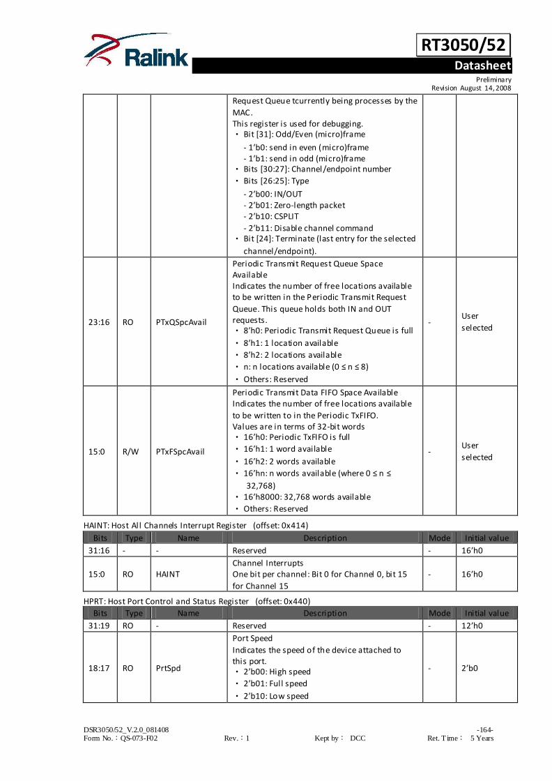
RT3050/52 Datasheet
Preliminary Revision August 14, 2008
DSR3050/52_V.2.0_081408 -164- Form No.:QS-073-F02 Rev.:1 Kept by: DCC Ret. T ime: 5 Years
Request Queue tcurrently being processes by the
MAC. This register is used for debugging. • Bit [31]: Odd/Even (micro)frame
- 1’b0: send in even (micro)frame - 1’b1: send in odd (micro)frame
• Bits [30:27]: Channel/endpoint number
• Bits [26:25]: Type
- 2’b00: IN/OUT - 2’b01: Zero-length packet - 2’b10: CSPLIT
- 2’b11: Disable channel command • Bit [24]: Terminate (last entry for the selected
channel/endpoint).
23:16 RO PTxQSpcAvail
Periodic Transmit Request Queue Space Available Indicates the number of free locations available to be written in the Periodic Transmit Request
Queue. This queue holds both IN and OUT requests. • 8’h0: Periodic Transmit Request Queue is full
• 8’h1: 1 location available
• 8’h2: 2 locations available
• n: n locations available (0 ≤ n ≤ 8)
• Others: Reserved
- User
selected
15:0 R/W PTxFSpcAvail
Periodic Transmit Data FIFO Space Available Indicates the number of free locations available
to be written to in the Periodic TxFIFO. Values are in terms of 32-bit words • 16’h0: Periodic TxFIFO is full
• 16’h1: 1 word available
• 16’h2: 2 words available
• 16’hn: n words available (where 0 ≤ n ≤
32,768) • 16’h8000: 32,768 words available
• Others: Reserved
- User
selected
HAINT: Host Al l Channels Interrupt Register (offset: 0x414)
Bits Type Name Description Mode Initial value
31:16 - - Reserved - 16’h0
15:0 RO HAINT Channel Interrupts One bit per channel: Bit 0 for Channel 0, bit 15
for Channel 15
- 16’h0
HPRT: Host Port Control and Status Register (offset: 0x440)
Bits Type Name Description Mode Initial value
31:19 RO - Reserved - 12’h0
18:17 RO PrtSpd
Port Speed
Indicates the speed of the device attached to this port. • 2’b00: High speed
• 2’b01: Full speed
• 2’b10: Low speed
- 2’b0

RT3050/52 Datasheet
Preliminary Revision August 14, 2008
DSR3050/52_V.2.0_081408 -165- Form No.:QS-073-F02 Rev.:1 Kept by: DCC Ret. T ime: 5 Years
•2’b11: Reserved
16:13 R/W PrtTstCtl
Port Test Control The application writes a nonzero value to this field to put the port into a Test mode, and the
corresponding pattern is signaled on the port. • 4’b0000: Test mode disabled
• 4’b0001: Test_J mode
• 4’b0010: Test_K mode
• 4’b0011: Test_SE0_NAK mode
• 4’b0100: Test_Packet mode
• 4’b0101: Test_Force_Enable
• Others: Reserved
- 4’h0
12 R_W_SC
PrtPwr
Port Power The application uses this field to control power to this port, and the core clears this bit on an overcurrent condition. • 1’b0: Power off
• 1’b1: Power on
- 1’b0
11:10 RO PrtLnSts
Port Line Status
Indicates the current logic level USB data lines • Bit [10]: Logic level of D+
• Bit [11]: Logic level of D–
- 2’b0
9 - - Reserved - 1’b0
8 R/W PrtRst
Port Reset When the application sets this bit, a reset
sequence is started on this port. The application must time the reset period and clear this bit after the reset
sequence is complete. • 1’b0: Port not in reset
• 1’b1: Port in reset
The application must leave this bit set for at least a minimum duration mentioned below to start a reset on the port. The application can leave it set for another 10 ms in addition to the required
minimum duration, before clearing the bit, even though there is no maximum limit set by the USB standard. • High speed: 50 ms
• Full speed/Low speed: 10 ms
- 1’b0
7 R_WS_SC
PrtSusp
Port Suspend
The application sets this bit to put this port in Suspend mode. The core only stops sending SOFs when this is set. To stop the PHY clock, the application must set
the Port Clock Stop bit, which asserts the suspend input pin of the PHY. The read value of this bit reflects the current suspend status of the port. This bit is cleared by
the core after a remote wakeup signal is detected or the application sets the Port Reset bit or Port Resume bit in this register or the
- 1’b0

RT3050/52 Datasheet
Preliminary Revision August 14, 2008
DSR3050/52_V.2.0_081408 -166- Form No.:QS-073-F02 Rev.:1 Kept by: DCC Ret. T ime: 5 Years
Resume/Remote Wakeup Detected Interrupt bit
or Disconnect Detected Interrupt bit in the Core Interrupt register (GINTSTS.WkUpInt or GINTSTS.DisconnInt, respectively). • 1’b0: Port not in Suspend mode
• 1’b1: Port in Suspend mode
6 R_W_SS_SC
PrtRes
Port Resume The application sets this bit to drive resume
signaling on the port. The core continues to drive the resume signal until the application clears this bit.
If the core detects a USB remote wakeup sequence, as indicated by the Port Resume/Remote Wakeup Detected Interrupt bit of the Core Interrupt register(GINTSTS.WkUpInt),
the core starts driving resume signaling without application intervention and clears this bit when it detects a disconnect condition. The read value of this bit indicates whether the core is currently
driving resume signaling. • 1’b0: No resume driven
• 1’b1: Resume driven
- 1’b0
5 R_SS_WC
PrtOvrCurrChng
Port Overcurrent Change The core sets this bit when the status of the Port Overcurrent Active bit (bit 4) in this register
changes.
- 1’b0
4 RO PrtOvrCurrAct
Port Overcurrent Active Indicates the overcurrent condition of the port. • 1’b0: No overcurrent condition
• 1’b1: Overcurrent condition
- 1’b0
3 R_SS_
WC PrtEnChng
Port Enable/Disable Change The core sets this bit when the status of the Port
Enable bit [2] of this register changes.
- 1’b0
2 R_SS_SC_W
C
PrtEna
Port Enable A port is enabled only by the core after a reset sequence, and is disabled by an overcurrent
condition, a disconnect condition, or by the application clearing this bit. The application cannot set this bit by a register write. It can only
clear it to disable the port. This bit does not trigger any interrupt to the application. • 1’b0: Port disabled
• 1’b1: Port enabled
- 1’b0
1 R_SS_WC
PrtConnDet
Port Connect Detected The core sets this bit when a device connection is detected to trigger an interrupt to the
application using the Host Port Interrupt bit of the Core Interrupt register (GINTSTS.PrtInt). The application must write a 1 to this bit to clear
the interrupt.
- 1’b0
0 RO PrtConnSts
Port Connect Status • 0: No device is attached to the port.
• 1: A device is attached to the port. 1’b0

RT3050/52 Datasheet
Preliminary Revision August 14, 2008
DSR3050/52_V.2.0_081408 -167- Form No.:QS-073-F02 Rev.:1 Kept by: DCC Ret. T ime: 5 Years
HCCHARn: Host Channel -n Characteristics Register
Channel_number: 0 ≤ n ≤ 15
(Offset: 500h + (Channel_number * 20h))
Bits Type Name Description Mode Initial value
31 R_WS_SC
ChEna
Channel Enable This field is set by the application and cleared by
the OTG host • 1’b0: Channel disabled
• 1’b1: Channel enabled
- 1’b0
30 R_WS
_SC ChDis
Channel Disable The application sets this bit to stop transmitting/receiving data on a channel, even before the transfer for that channel is complete.
The application must wait for the Channel Disabled interrupt before treating the channel as disabled.
- 1’b0
29 R/W OddFrm
Odd Frame This field is set (reset) by the application to indicate that the OTG host must perform a transfer in an odd (micro)frame. This field is
applicable for only periodic (isochronous and interrupt) transactions. • 1’b0: Even (micro)frame
• 1’b1: Odd (micro)frame
- 1’b0
28:22 R/W DevAddr Device Address This field selects the specific device serving as the data source or sink.
- 7’h0
21:20 R/W MC/ EC
Multi Count/ / Error Count When the Spl it Enable bit of the Host Channel -n Split Control register (HCSPLTn.SpltEna) is reset
(1’b0), this field indicates to the host the number of transactions that must be executed per microframe for this periodic endpoint. For non periodic transfers, this field is used only in DMA
mode, and specifies the number packets to be fetched for this channel before the internal DMA engine changes arbitration. • 2’b00: Reserved This field yields undefined
results. • 2’b01: 1 transaction
• 2’b10: 2 transactions to be issued for this
endpoint per microframe • 2’b11: 3 transactions to be issued for this
endpoint per microframe When HCSPLTn.SpltEna is set (1’b1), this field indicates the number of immediate retries to be performed for a periodic split transactions on
transaction errors. This field must be set to at least 2’b01.
- 2’b0
19:18 R/W EPType
Endpoint Type Indicates the transfer type selected. • 2’b00: Control
- 2’b0

RT3050/52 Datasheet
Preliminary Revision August 14, 2008
DSR3050/52_V.2.0_081408 -168- Form No.:QS-073-F02 Rev.:1 Kept by: DCC Ret. T ime: 5 Years
• 2’b01: Isochronous
• 2’b10: Bulk
• 2’b11: Interrupt
17 R/W LSpdDev
Low-Speed Device
This field is set by the application to indicate that this channel is communicating to a low-speed device.
- 1’b0
16 - - Reserved - 1’b0
15 R/W EPDir
Endpoint Direction Indicates whether the transaction is IN or OUT. • 1’b0: OUT
• 1’b1: IN
- 1’b0
14:11 R/W EPNum
Endpoint Number
Indicates the endpoint number on the device serving as the data source or sink.
- 4’h0
10:0 R/W MPS Maximum Packet Size Indicates the maximum packet size of the
associated endpoint.
- 11’h0
HCSPLTn: Host Channel -n Split Control Register
Channel_number: 0 ≤ n ≤ 15
(Offset: 504h + (Channel_number * 20h))
Bits Type Name Description Mode Initial value
31 R/W SpltEna Split Enable The application sets this field to indicate that this
channel is enabled to perform split transactions.
- 1’b0
30:17 - - Reserved - 14’h0
16 R/W CompSplt Do Complete Split The application sets this field to request the OTG host to perform a complete split transaction.
- 1’b0
15:14 R/W XactPos
Transaction Position
This field is used to determine whether to send all, first, middle, or last payloads with each OUT transaction. • 2’b11: All. This is the entire data payload is of
this transaction (which is less than or equal to 188 bytes).
• 2’b10: Begin. This is the first data payload of
this transaction (which is larger than 188 bytes).
• 2’b00: Mid. This is the middle payload of this
transaction (which is larger than 188 bytes). • 2’b01: End. This is the last payload of this
transaction (which is larger than 188 bytes).
- 2’h0
13:7 R/W HubAddr Hub Address This field holds the device address of the transaction translator’s hub.
- 7’h0
6:0 R/W PrtAddr
Port Address
This field is the port number of the recipient transaction translator.
- 7’h0

RT3050/52 Datasheet
Preliminary Revision August 14, 2008
DSR3050/52_V.2.0_081408 -169- Form No.:QS-073-F02 Rev.:1 Kept by: DCC Ret. T ime: 5 Years
HCINTn: Host Channel -n Interrupt Register
Channel_number: 0 ≤ n ≤ 15
(Offset: 508h + (Channel_number * 20h))
Bits Type Name Description Mode Initial value
31:11 - - Reserved - 21’h0
10 R_SS_WC
DataTglEr Data Toggle Error - 1’b0
9 R_SS_
WC FrmOvrun Frame Overrun - 1’b0
8 R_SS_WC
BblErr Babble Error - 1’b0
7 R_SS_WC
XactErr
Transaction Error
Indicates one of the following errors occurred on the USB. • CRC check failure • Timeout
• Bit stuff error •False EOP
- 1’b0
6 R_SS_
WC NYET NYET Response Received Interrupt - 1’b0
5 R_SS_WC
ACK ACK Response Received/Transmitted Interrupt - 1’b0
4 R_SS_
WC NAK NAK Response Received Interrupt - 1’b0
3 R_SS _WC
STALL STALL Response Rec eived Interrupt - 1’b0
2 R_SS_WC
AHBErr
AHB Error This is generated only in Internal DMA mode when there is an AHB error during AHB read/write. The application can read the
corresponding channel’s DMA address register to get the error address.
- 1’b0
1 R_SS_
WC ChHltd
Channel Halted Indicates the transfer completed abnormally
either because of any USB transaction error or in response to disable request by the application.
- 1’b0
0 R_SS_
WC XferCompl
Transfer Completed
Transfer completed normally without any errors. - 1’b0
HCINTMSKn: Host Channel -n Interrupt Mask Register
Channel_number: 0 ≤ n ≤ 15
(Offset: 50Ch + (Channel_number * 20h))
Bits Type Name Description Mode Initial value
31:11 - - Reserved - 21’h0
10 R/W DataTglErrMsk Data Toggle Error Mask - 1’b0
9 R/W FrmOvrunMsk Frame Overrun Mask - 1’b0
8 R/W BblErrMsk Babble Error Mask - 1’b0
7 R/W XactErrMsk Transaction Error Mask - 1’b0
6 R/W NyetMsk NYET Response Received Interrupt Mask - 1’b0
5 R/W AckMsk ACK Response Received/Transmitted Interrupt Mask
- 1’b0

RT3050/52 Datasheet
Preliminary Revision August 14, 2008
DSR3050/52_V.2.0_081408 -170- Form No.:QS-073-F02 Rev.:1 Kept by: DCC Ret. T ime: 5 Years
4 R/W NakMsk NAK Response Received Interrupt Mask - 1’b0
3 R/W StallMsk STALL Response Rec eived Interrupt Mask - 1’b0
2 R/W AHBErrMsk AHB Error Mask - 1’b0
1 R/W ChHltdMsk Channel Halted Mask - 1’b0
0 R/W XferComplMsk Transfer Completed Mask - 1’b0
HCTSIZn: Host Channel -n Interrupt Mask Register
Channel_number: 0 ≤ n ≤ 15
(Offset: 510h + (Channel_number * 20h))
Bits Type Name Description Mode Initial value
31 R/W DoPng Setting this field to 1 directs the host to do PING
protocol - 1’h0
30:29 R/W Pid
PID The application programs this field with the type
of PID to use for the initial transaction. The host maintains this field for the rest of the transfer. • 2’b00: DATA0 • 2’b01: DATA2
• 2’b10: DATA1 • 2’b11: MDATA (non-control)/SETUP (control)
- 2’b0
28:19 R/W PktCnt
Packet Count This field is programmed by the application with
the expected number of packets to be transmitted (OUT) or received (IN). The host decrements this count on every
successful transmission or reception of an OUT/IN packet. Once this count reaches zero, the application is interrupted to indicate normal completion.
The width of this counter is specified as Width of Packet Counters during coreConsultant configuration (parameter OTG_PACKET_
COUNT_WIDTH).
- 10’b0
18:0 R/W XferSize
Transfer Size For an OUT, this field is the number of data bytes the host sends during the transfer.
For an IN, this field is the buffer size that the application has Reserved for the transfer. The application is expected to program this field as an integer multiple of the maximum packet size
for IN transactions (periodic and non-periodic). The width of this counter is specified as Width of Transfer Size Counters during coreConsultant
configuration (parameter OTG_TRANS_ COUNT_WIDTH).
- 19’b0
HCDMAn: Host Channel -n DMA Address Register
Channel_number: 0 ≤ n ≤ 15
(Offset: 514h + (Channel_number * 20h))
Bits Type Name Description Mode Initial value
31:0 R/W DMAAddr DMA Address This field holds the start address in the external
memory from which the data for the endpoint
- 32’h0

RT3050/52 Datasheet
Preliminary Revision August 14, 2008
DSR3050/52_V.2.0_081408 -171- Form No.:QS-073-F02 Rev.:1 Kept by: DCC Ret. T ime: 5 Years
must be fetched or to which it must be stored.
This register is incremented on every AHB transaction.
DCFG: Device Configuration Register (offset: 0x800)
Bits Type Name Description Mode Initial value
31:23 - - Reserved - 9’h0
22:18 R/W EPMisCnt
IN Endpoint Mismatch Count This field is valid only in shared FIFO operation. The application programs this filed with a count
that determines when the core generates an Endpoint Mismatch interrupt (GINTSTS.EPMis). The core loads this value into an internal counter and decrements it. The counter is reloaded
whenever there is a match or when the counter expires. The width of this counter depends on the depth of the Token Queue.
- 5’h8
17:13 - - Reserved - 5’h0
12:11 R/W PerFrInt
Periodic Frame Interval Indicates the time within a (micro)frame at
which the application must be notified using the End Of Periodic Frame Interrupt. This can be used to determine if all the isochronous traffic for that (micro)frame is complete.
• 2’b00: 80% of the (micro)frame interval • 2’b01: 85% • 2’b10: 90%
• 2’b11: 95%
- 2’h0
10:4 R/W DevAddr
Device Address The application must program this field after every SetAddress control command.
- 7’h0
3 - - Reserved - 1’b0
2 R/W NZStsOUTHShk
Non-Zero-Length Status OUT Handshake
The application can use this field to select the handshake the core sends on receiving a nonzero-length data packet during the OUT transaction of a control transfer’s Status stage.
• 1’b1: Send a STALL handshake on a nonzero- length status OUT transaction and do not send
the rec eived OUT packet to the application.
• 1’b0: Send the rec eived OUT packet to the application (zero-length or nonzero-length)
and send a handshake based on the NAK and STALL bits for the endpoint in the Device
Endpoint Control register.
- 1’b0
1:0 R/W DevSpd
Device Speed Indicates the speed at which the application requires the core to enumerate, or the
maximum speed the application can support. However, the actual bus speed is determined only after the chirp sequence is completed, and
is based on the speed of the USB host to which the core is connected. See “Device Initialization” on page 297 for details.
- 2’b0

RT3050/52 Datasheet
Preliminary Revision August 14, 2008
DSR3050/52_V.2.0_081408 -172- Form No.:QS-073-F02 Rev.:1 Kept by: DCC Ret. T ime: 5 Years
• 2’b00: High speed (USB 2.0 PHY clock is 30
MHz or 60 MHz) • 2’b01: Full speed (USB 2.0 PHY clock is 30 MHz
or 60 MHz) • 2’b10: Low speed (USB 1.1 transceiver clock is
6 MHz). If you select 6 MHz LS mode, you must do a soft reset
. • 2’b11: Full speed (USB 1.1 transceiver clock is
48 MHz)
DCTL: Device Control Register (offset: 0x804)
Bits Type Name Description Mode Initial value
31:12 - - Reserved - 20’h0
11 R/W PWROnPrgDone
Power-On Programming Done
The application uses this bit to indicate that register programming is completed after a wake-up from Power Down mode. For more
information, see “Device Mode Suspend and Resume With Partial Power-Down” on page 422.
- 1’b0
10 WO CGOUTNak Clear Global OUT NAK A write to this field clears the Global OUT NAK.
- 1’b0
9 WO SGOUTNak
Set Global OUT NAK A write to this field sets the Global OUT NAK. The application uses this bit to send a NAK handshake on all OUT endpoints.
The application must set the this bit only after making sure that the Global OUT NAK Effective bit in the Core Interrupt Register
(GINTSTS.GOUTNakEff) is cleared.
- 1’b0
8 WO CGNPInNak Clear Global Non-periodic IN NAK A write to this field clears the Global Non-periodic IN NAK.
- 1’b0
7 WO SGNPInNak
Set Global Non-periodic IN NAK A write to this field sets the Global Non-periodic IN NAK. The application uses this bit to send a NAK
handshake on all non-periodic IN endpoints. The core can also set this bit when a timeout condition is detected on a non-periodic endpoint
in shared FIFO operation. The application must set this bit only after making sure that the Global IN NAK Effective bit in the Core Interrupt Register
(GINTSTS.GINNakEff) is cleared.
- 1’b0
6:4 R/W TstCtl
Test Control • 3’b000: Test mode disabled
• 3’b001: Test_J mode • 3’b010: Test_K mode • 3’b011: Test_SE0_NAK mode • 3’b100: Test_Packet mode
• 3’b101: Test_Force_Enable • Others: Reserved
- 3’b0
3 RO GOUTNakSts Global OUT NAK Status • 1’b0: A handshake is sent based on the FIFO
- 1’b0

RT3050/52 Datasheet
Preliminary Revision August 14, 2008
DSR3050/52_V.2.0_081408 -173- Form No.:QS-073-F02 Rev.:1 Kept by: DCC Ret. T ime: 5 Years
Status and the NAK and STALL bit settings.
• 1’b1: No data is written to the RxFIFO, irrespective of space availability. Sends a NAK handshake on all packets, except on SETUP transactions.
All isochronous OUT packets are dropped.
2 RO GNPINNakSts
Global Non-periodic IN NAK Status • 1'b0: A handshake is sent out based on the
data availability in the transmit FIFO. • 1'b1: A NAK handshake is sent out on all non-
periodic IN endpoints, irrespective of the data availability in the transmit FIFO.
- 1’b0
1 R/W SftDiscon
Soft Disconnect The application uses this bit to signal the DWC_otg core to do a soft disconnect. As long as this bit is set, the host does not see that the
device is connected, and the device does not receive signals on the USB. The core stays in the disconnected state until the application clears
this bit. The minimum duration for which the core must keep this bit set is specified in Table 5-45. • 1’b0: Normal operation. When this bit is
cleared after a soft disconnect, the core drives the phy_opmode_o signal on the UTMI+ to 2’b00, which generates a device connect
event to the USB host. When the device is reconnected, the USB host restarts device enumeration.
• 1’b1: The core drives the phy_opmode_o
signal on the UTMI+ to 2’b01, which generates a device disconnect event to the USB host.
- 1’b0
0 R/W RmtWkUpSig
Remote Wakeup Signaling
When the application sets this bit, the core initiates remote signaling to wake up the USB host.
The application must set this bit to instruct the core to exit the Suspend state. As specified in the USB 2.0 specification, the application must clear this bit 1–15 ms after setting it.
- 1’b0
DSTS: Device Status Register (offset: 0x808)
Bits Type Name Description Mode Initial value
31:22 - - Reserved - 10’h0
21:8 RO SOFFN
Frame or Microframe Number of the Received
SOF When the core is operating at high speed, this field contains a microframe number. When the core is operating at full or low speed, this field
contains a frame number.
- 14’h0
7:4 - - Reserved - 4’h0
3 RO ErrticErr Erratic Error The core sets this bit to report any erratic errors
- 1’b0
RT3050/52 Datasheet
Preliminary Revision August 14, 2008
DSR3050/52_V.2.0_081408 -174- Form No.:QS-073-F02 Rev.:1 Kept by: DCC Ret. T ime: 5 Years
(phy_rxvalid_i/ phy_rxvldh_i or phy_rxactive_i is
asserted for at least 2 ms, due to PHY error) seen on the UTMI+ . Due to erratic errors, the DWC_otg core goes into Suspended state and an interrupt is
generated to the application with Early Suspend bit of the Core Interrupt register (GINTSTS.ErlySusp). If the early suspend is
asserted due to an erratic error, the application can only perform a soft disconnect recover
2:1 RO EnumSpd
Enumerated Speed Indicates the speed at which the DWC_otg core
has come up after speed detection through a chirp sequence. • 2’b00: High speed (PHY clock is running at 30
or 60 MHz)
• 2’b01: Full speed (PHY clock is running at 30 or 60 MHz)
• 2’b10: Low speed (PHY clock is running at 6
MHz) • 2’b11: Full speed (PHY clock is running at 48
MHz) Low speed is not supported for devices using a UTMI+ PHY.
- 2’h01
0 RO SuspSts
Suspend Status In Device mode, this bit is set as long as a Suspend condition is detected on the USB. The
core enters the Suspended state when there is no activity on the phy_line_state_i signal for an extended period of time. The core comes out of the suspend:
• When there is any activity on the phy_line_state_i signal
• When the application writes to the Remote Wakeup Signaling bit in the Device Control
register (DCTL.RmtWkUpSig).
- 1’b0
DIEPMSK: Device IN Endpoint Common Interrupt Mask Register (offset: 0x810)
Bits Type Name Description Mode Initial value
31:9 - - Reserved - 23’h0
8 R/W TxfifoUndrnMsk Fifo Underrun Mask - 1’b0
7 R/W - Reserved - 1’b0
6 R/W INEPNakEffMsk IN Endpoint NAK Effective Mask - 1’b0
5 R/W INTknEPMisMsk IN Token received with EP Mismatch Mask - 1’b0
4 R/W INTknTXFEmpMsk IN Token Received When TxFIFO Empty Mask - 1’b0
3 R/W
TimeOUTMsk Timeout Condition Mask (Non-isochronous endpoints)
- 1’b0
2 R/W AHBErrMsk AHB Error Mask - 1’b0
1 R/W EPDisbldMsk Endpoint Disabled Interrupt Mask - 1’b0
0 R/W XferComplMsk Transfer Completed Interrupt Mask - 1’b0
DOEPMSK: Device OUT Endpoint Common Interrupt Mask Register (offset: 0x814)
Bits Type Name Description Mode Initial value
31:9 - - Reserved - 23’h0

RT3050/52 Datasheet
Preliminary Revision August 14, 2008
DSR3050/52_V.2.0_081408 -175- Form No.:QS-073-F02 Rev.:1 Kept by: DCC Ret. T ime: 5 Years
8 R/W OutPktErrMsk OUT Packet Error Mask - 1’b0
7 - - Reserved - 1’b0
6 R/W Back2BackSETup Back-to-Back SETUP Packets Received Mask Applies to control OUT endpoints only.
- 1’b0
5 - - Reserved - 1’b0
4 R/W OUTTknEPdisMsk OUT Token Received when Endpoint Disabled Mask Applies to control OUT endpoints only.
- 1’b0
3 R/W SetUPMsk SETUP Phase Done Mask Applies to control endpoints only.
- 1’b0
2 R/W AHBErrMsk AHB Error - 1’b0
1 R/W EPDisbldMsk Endpoint Disabled Interrupt Mask - 1’b0
0 R/W XferComplMsk Transfer Completed Interrupt Mask - 1’b0
DAINT: Device All Endpoints Interrupt Register (offset: 0x818)
Bits Type Name Description Mode Initial value
31:16 RO OutEPInt OUT Endpoint Interrupt Bits One bit per OUT endpoint: Bit 16 for OUT endpoint 0, bit 31 for OUT endpoint 15
- 16’h0
15:0 RO InEpInt IN Endpoint Interrupt Bits One bit per IN Endpoint: Bit 0 for IN endpoint 0, bit 15 for endpoint 15
- 16’h0
DAINTMSK: Device Endpoints Interrupt Mask Register (offset: 0x81c)
Bits Type Name Description Mode Initial value
31:16 R/W OutEpMsk
OUT EP Interrupt Mask Bits
One per OUT Endpoint: Bit 16 for OUT EP 0, bit 31 for OUT EP 15
- 16’h0
15:0 R/W (InEpMsk IN EP Interrupt Mask Bits One bit per IN Endpoint: Bit 0 for IN EP 0, bit 15
for IN EP 15
- 16’h0
DTKNQR1:Device IN Token Sequence Learning Queue Read Register 1(offset: 0x820)
Bits Type Name Description Mode Initial value
31:8 RO EPTkn
Endpoint Token Four bits per token represent the endpoint number of the token:
• Bits *31:28+: Endpoint number of Token 5 • Bits *27:24+: Endpoint number of Token 4 ....... • Bits *15:12+: Endpoint number of Token 1
• Bits *11:8+: Endpoint number of Token 0
- 24’h0
7 RO WrapBit Wrap Bit This bit is set when the write pointer wraps. It is
cleared when the learning queue is cleared.
- 1’b0
6:5 RO - Reserved - 2’h0
4:0 RO INTknWPtr IN Token Queue Write Pointer - 5’h0
DTKNQR2:Device IN Token Sequence Learning Queue Register 2 (offset: 0x824)
Bits Type Name Description Mode Initial value
31:0 RO EPTkn
Endpoint Token Four bits per token represent the endpoint
number of the token: • Bits *31:28+: Endpoint number of Token 13 • Bits *27:24+: Endpoint number of Token 12
- 32’h0

RT3050/52 Datasheet
Preliminary Revision August 14, 2008
DSR3050/52_V.2.0_081408 -176- Form No.:QS-073-F02 Rev.:1 Kept by: DCC Ret. T ime: 5 Years
.......
• Bits *7:4+: Endpoint number of Token 7 • Bits *3:0+: Endpoint number of Token 6
DTKNQR3:Device IN Token Sequence Learning Queue Register 3 (offset: 0x0830)
Bits Type Name Description Mode Initial value
31:0 RO EPTkn
Endpoint Token Four bits per token represent the endpoint
number of the token: • Bits *31:28+: Endpoint number of Token 21 • Bits *27:24+: Endpoint number of Token 20 .......
• Bits *7:4+: Endpoint number of Token 15 • Bits *3:0+: Endpoint number of Token 14
- 32’h0
DTKNQR4:Device IN Token Sequence Learning Queue Register 4 (offset: 0x0834)
Bits Type Name Description Mode Initial value
31:0 RO EPTkn
Endpoint Token
Four bits per token represent the endpoint number of the token: • Bits *31:28+: Endpoint number of Token 29 • Bits *27:24+: Endpoint number of Token 28
....... • Bits *7:4+: Endpoint number of Token 23 • Bits *3:0+: Endpoint number of Token 22
- 32’h0
DVBUSDIS: Device VBUS Discharge Time Register (offset: 0x0828)
Bits Type Name Description Mode Initial value
31:16 - - Reserved - 16’h0
15:0 R/W DVBUSDis
Device VBUS Discharge Time Specifies the VBUS discharge time after VBUS
pulsing during SRP. This value equals: VBUS discharge time in PHY clocks / 1, 024
The value you use depends whether the PHY is operating at 30 MHz (16-bit data width) or 60
MHz (8-bit data width). Depending on your VBUS load, this value can need adjustment.
-
30 MHz:
16’h0B8F 60 MHz:
16’h17D7
DVBUSPULSE: Device VBUS Pulsing Time Register (offset: 0x082c)
Bits Type Name Description Mode Initial value
31:12 - - Reserved - 20’h0
11:0 R/W DVBUSPulse
Device VBUS Pulsing Time Specifies the VBUS pulsing time during SRP. This value equals: VBUS pulsing time in PHY clocks /
1, 024 The value you use depends whether the PHY is operating at 30 MHz (16-bit data width) or 60
MHz (8-bit data width).
-
30 MHz: 12’h2C6
60 MHz: 12’h5B8
DTHRCTL:Device Threshold Control Register (offset: 0x830)
Bits Type Name Description Mode Initial value
31:28 - - Reserved - 4'b0
27 R/W ArbPrkEn
Arbiter Parking Enable
This bit controls internal DMA arbiter parking for IN endpoints. When thresholding is enabled and
- 1’b1

RT3050/52 Datasheet
Preliminary Revision August 14, 2008
DSR3050/52_V.2.0_081408 -177- Form No.:QS-073-F02 Rev.:1 Kept by: DCC Ret. T ime: 5 Years
this bit is set to one, then the arbiter parks on
the IN endpoint for which there is a token received on the USB. This is done to avoid getting into underrun conditions. By default the parking is enabled.
26 - - Reserved - 1’b1
25:17 R/W RxThrLen
Receive Threshold Length
This field specifies Receive thresholding size in DWORDS. This field also specifies the amount of data received on the USB before the core can start
transmitting on the AHB. The threshold length has to be at least eight DWORDS.
The recommended value for ThrLen is to be the same as the programmed AHB Burst Length (GAHBCFG.HBstLen).
- 9’h8
16 R/W RxThrEn
Receive Threshold Enable
When this bit is set, the core enables thresholding in the receive direction.
- 1’b0
15:11 - - Reserved - 5'b0
10:2 R/W TxThrLen
Transmit Threshold Length This field specifies Transmit thresholding size in DWORDS.
This field specifies the amount of data in bytes to be in the corresponding endpoint transmit FIFO, before the core can start transmit on the USB. The threshold length has to be at least eight
DWORDS. This field controls both isochronous and non-isochronous IN endpoint thresholds. The recommended value for ThrLen is to be the
same as the programmed AHB Burst Length (GAHBCFG.HBstLen).
- 9’h8
1 R/W ISOThrEn ISO IN Endpoints Threshold Enable. When this bit is set, the core enables
thresholding for isochronous IN endpoints.
- 1’b0
0 R/W NonISOThrEn Non-ISO IN Endpoints Threshold Enable. When this bit is set, the core enables thresholding for Non Isochronous IN endpoints.
- 1’b0
DIEPEMPMSK: Device IN Endpoint FIFO Empty Interrupt Mask Register (offset: 0x834)
Bits Type Name Description Mode Initial value
31:16 RO - Reserved - 16’h0
15:0 R/W InEpTxfEmpMsk
IN EP Tx FIFO Empty Interrupt Mask Bits
These bits acts as mask bits for DIEPINTn. TxFEmp interrupt One bit per IN Endpoint: Bit 0 for IN EP 0, bit 15 for IN EP 15
- 16’h0
DIEPCTL0 :Device Control IN Endpoint 0 Control Register (offset: 0x900)
Bits Type Name Description Mode Initial value
31 R/WS
/SC EPEna
Endpoint Enable
Indicates that data is ready to be transmitted on the endpoint. The core clears this bit before setting any of the following interrupts on this
- 1’b0

RT3050/52 Datasheet
Preliminary Revision August 14, 2008
DSR3050/52_V.2.0_081408 -178- Form No.:QS-073-F02 Rev.:1 Kept by: DCC Ret. T ime: 5 Years
endpoint:
• Endpoint Disabled • Transfer Completed
30 R/WS
/SC EPDis
Endpoint Disable The application sets this bit to stop transmitting
data on an endpoint, even before the transfer for that endpoint is complete. The application must wait for the Endpoint Disabled interrupt
before treating the endpoint as disabled. The core clears this bit before setting the Endpoint Disabled Interrupt. The application must set this bit only if Endpoint Enable is already set for this
endpoint.
- 1’b0
29:28 - - Reserved - 2’b0
27 WO SNAK
Set NAK A write to this bit sets the NAK bit for the endpoint. Using this bit, the application can control the transmission of NAK handshakes on
an endpoint. The core can also set this bit for an endpoint after a SETUP packet is received on that endpoint.
- 1’b0
26 WO CNAK
Clear NAK
A write to this bit clears the NAK bit for the endpoint.
- 1’b0
25:22 R/W TxFNum
TxFIFO Number
• For Shared FIFO operation, this value is always set to 0, indicating that control IN endpoint 0 data is always written in the Non-Periodic Transmit FIFO.
• For Dedicated FIFO operation, this value is set to the FIFO number that is assigned to IN Endpoint 0.
- 4’h0
21 R/WS
/SC Stall
STALL Handshake
The application can only set this bit, and the core clears it, when a SETUP token is received for this endpoint. If a NAK bit, Global Non-periodic IN
NAK, or Global OUT NAK is set along with this bit, the STALL bit takes priority.
- 1’b0
20 - - Reserved - 1’b0
19:18 RO EPType Endpoint Type Hardcoded to 00 for control.
- 2’h0
17 RO NAKSts
NAK Status
Indicates the following: • 1’b0: The core is transmitting non-NAK
handshakes based on the FIFO status • 1’b1: The core is transmitting NAK handshakes
on this endpoint. When this bit is set, either by the application or core, the core stops transmitting data, even if
there is data available in the TxFIFO. Irrespective of this bit’s setting, the core always responds to SETUP data packets with an ACK handshake.
- 1’b0
16 - - Reserved - 1’b0
RT3050/52 Datasheet
Preliminary Revision August 14, 2008
DSR3050/52_V.2.0_081408 -179- Form No.:QS-073-F02 Rev.:1 Kept by: DCC Ret. T ime: 5 Years
15 RO USBActEP
USB Active Endpoint
This bit is always set to 1, indicating that control endpoint 0 is always active in all configurations and interfaces.
- 1’b1
14:11 R/W NextEp
Next Endpoint
Applies to non-periodic IN endpoints only. Indicates the endpoint number to be fetched after the data for the current endpoint is
fetched. The core can access this field, even when the Endpoint Enable (EPEna) bit is not set. This field is not valid in Slave mode. Note: This field is valid only for Shared FIFO
operations.
- 4’b0
10:2 - - Reserved - 9’h0
1:0 R/W MPS
Maximum Packet Size Applies to IN and OUT endpoints. The application must program this field with the maximum packet size for the current logical
endpoint. • 2’b00: 64 bytes • 2’b01: 32 bytes • 2’b10: 16 bytes
• 2’b11: 8 bytes
- 2’h0

RT3050/52 Datasheet
Preliminary Revision August 14, 2008
DSR3050/52_V.2.0_081408 -180- Form No.:QS-073-F02 Rev.:1 Kept by: DCC Ret. T ime: 5 Years
3.20 802.11n 2T2R MAC/BBP
3.20.1 Features
1x1/1x2/2x1/2x2 modes.
300MHz PHY Rate Support.
Legacy and High Throughput Modes.
20MHz/40MHz bandwidth.
Reverse Direction Data Flow and Frame Aggregation
WEP 64/128, WPA, WPA2 Support
QoS – WMM, WMM-PS
Wake on Wireless LAN
Multiple BSSID Support
International Regulation - 802.11d +h
Cisco CCX V1.0 V2.0 V3.0 Compliance
Bluetooth Co-existence
Low Power with Advanced Power Management
3.20.2 Block Diagram
WPDMA SEC PBF MAC
BBP/
ADC/
DAC
WMM
SCH
Rbus
PalmBus
CSR
Packet
BufferSEC
Tables
Fig. 3-20-1 802.11n 2T2R MAC/BBP Block Diagram

RT3050/52 Datasheet
Preliminary Revision August 14, 2008
DSR3050/52_V.2.0_081408 -181- Form No.:QS-073-F02 Rev.:1 Kept by: DCC Ret. T ime: 5 Years
Fig. 3-20-2 802.11n 2T2R MAC/BBP Register Map
3.20.3 Register Description (base: 0x1018.0000)
3.20.3.1 Register Description - SCH/WPDMA (base: 1018.0000)
INT_STATUS: INT_STATUS Register (offset: 0x0200)
Bits Type Name Description Initial value
31:21 - - Reserved 0
20 R/W RADAR_INT BBP radar detection interrupt 0
19:18 - - Reserved 0
17 R/W TX_COHERENT TX_DMA finds data coherent event when checking ddone bit. Write 1 to clear the interrupt.
Read to get the raw interrupt status
0
16 R/W RX_COHERENT RX_DMA finds data coherent event when checking ddone bit. Write 1 to clear the interrupt.
0
MAC search table(800h)
Program memory (2000h)
MAC register (800h)
Reserved(200h)
CIS (100h)
Beacon frame (800h)
NULL frame (100h)
distributed register
SRAM (8KB)
SCH/WPDMA register (200h) 0200 h
0400 h
1000 h
1800 h
2000 h
0000 h
Packet buffer (8000 h)
8000 h
SYS/PBF/FCE/MISC register (400h)
FCE table (1000h)
4000 h MAC key table (2600h)
SRAM (32KB)
SRAM (16KB)
0800 h Reserved (800h)
SRAM (2KB)
RT3050/52 Datasheet
Preliminary Revision August 14, 2008
DSR3050/52_V.2.0_081408 -182- Form No.:QS-073-F02 Rev.:1 Kept by: DCC Ret. T ime: 5 Years
Read to get the raw interrupt status
15 R/W MAC_INT_4 MAC interrupt 4 : GP timer interrupt 0
14 R/W MAC_INT_3 MAC interrupt 3 : Auto wakeup interrupt 0
13 R/W MAC_INT_2 MAC interrupt 2 : TX status interrupt 0
12 R/W MAC_INT_1 MAC interrupt 1 : Pre-TBTT interrupt 0
11 R/W MAC_INT_0 MAC interrupt 0 : TBTT interrupt 0
10 RO TX_RX_COHERENT
When TX_COHERENT or RX_COHERENT is on, this bit is set 0
9 R/W MCU_CMD_INT MCU command interrupt 0
8 R/W TX_DONE_INT5 TX Queue#5 packet transmit interrupt Write 1 to clear the interrupt.
0
7 R/W TX_DONE_INT4 TX Queue#4 packet transmit interrupt Write 1 to clear the interrupt.
Read to get the raw interrupt status
0
6 R/W TX_DONE_INT3 TX Queue#3 packet transmit interrupt Write 1 to clear the interrupt. Read to get the raw interrupt status
0
5 R/W TX_DONE_INT2 TX Queue#2 packet transmit interrupt Write 1 to clear the interrupt.
Read to get the raw interrupt status
0
4 R/W TX_DONE_INT1 TX Queue#1 packet transmit interrupt Write 1 to clear the interrupt. Read to get the raw interrupt status
0
3 R/W TX_DONE_INT0 TX Queue#0 packet transmit interrupt Write 1 to clear the interrupt.
Read to get the raw interrupt status
0
2 R/W RX_DONE_INT RX packet receive interrupt Write 1 to clear the interrupt. Read to get the raw interrupt status
0
1 R/W TX_DLY_INT Summary of the whole WPDMA TX related interrupts Write 1 to clear the interrupt.
Read to get the raw interrupt status
0
0 R/W RX_DLY_INT
Summary of the whole WPDMA RX related interrupts Write 1
to clear the interrupt. Read to get the raw interrupt status
0
INT_MASK: INT_MASK Register (offset: 0x0204)
Bits Type Name Description Initial value
31:18 - - Reserved 0
20 R/W RADAR_INT_EN Enable for BBP radar detection interrupt 1: Enable the interrupt 0: Disable the interrupt
0
19:18 - - Reserved 0
17 R/W TX_COHERENT_EN
Enable for TX_DMA data coherent interrupt 1: Enable the interrupt 0: Disable the interrupt
0
16 R/W RX_COHERENT_
EN
Enable for RX_DMA data coherent interrupt
1: Enable the interrupt 0: Disable the interrupt
0
14 R/W MAC_INT4_EN MAC interrupt 4 : GP timer interrupt 0
14 R/W MAC_INT3_EN MAC interrupt 3 : Auto wakeup interrupt 0
13 R/W MAC_INT2_EN MAC interrupt 2 : TX status interrupt 0

RT3050/52 Datasheet
Preliminary Revision August 14, 2008
DSR3050/52_V.2.0_081408 -183- Form No.:QS-073-F02 Rev.:1 Kept by: DCC Ret. T ime: 5 Years
12 R/W MAC_INT1_EN MAC interrupt 1 : Pre-TBTT interrupt 0
11 R/W MAC_INT0_EN MAC interrupt 0 : TBTT interrupt 0
10 - - Reserved 0
9 R/W MCU_CMD_INT_
MSK
MCU command interrupt enable
1 : Enable the interrupt 0 : Disable the interrupt
0
8 R/W TX_DONE_INT_MSK5
TX Queue#5 packet transmit interrupt 1 : Enable the interrupt 0 : Disable the interrupt
0
7 R/W TX_DONE_INT_
MSK4
TX Queue#4 packet transmit interrupt
1 : Enable the interrupt 0 : Disable the interrupt
0
6 R/W TX_DONE_INT_MSK 3
TX Queue#3 packet transmit interrupt 1 : Enable the interrupt 0 : Disable the interrupt
0
5 R/W TX_DONE_INT_
MSK 2
TX Queue#2 packet transmit interrupt
1 : Enable the interrupt 0 : Disable the interrupt
0
4 R/W TX_DONE_INT_MSK 1
TX Queue#1 packet transmit interrupt 1 : Enable the interrupt 0 : Disable the interrupt
0
3 R/W TX_DONE_INT_
MSK 0
TX Queue#0 packet transmit interrupt
1 : Enable the interrupt 0 : Disable the interrupt
0
2 R/W RX_DONE_INT_MSK
RX packet receive interrupt 1 : Enable the interrupt 0 : Disable the interrupt
0
1 R/W TX_DLY_INT_
MSK
Summary of the whole WPDMA TX related interrupts
1 : Enable the interrupt 0 : Disable the interrupt
0
0 R/W RX_ DLY_INT_ MSK
Summary of the whole WPDMA RX related interrupts 1 : Enable the interrupt 0 : Disable the interrupt
0
WPDMA_GLO_CFG: WPDMA_GLO_CFG Register (offset: 0x0208)
Bits Type Name Description Initial value
31:16 - - Reserved 0
15:8 HDR_SEG_LEN
Specify the header segment size in byte to support RX
header/payload scattering function, when set to a non-zero value. When set to zero, the header/payload scattering feature is
disabled.
8’b0
7 R/W BIG_ENDIAN
The endian mode selection. DMA applies the endian rule to convert payload and TX/RX information. DMA won’t apply endian rule to register or descriptor. 1: big endian. 0: little endian.
0
6 R/W TX_WB_DDONE 0 :Disable TX_DMA writing back DDONE into TXD
1 : Enable TX_DMA writing back DDONE into TXD 1’b1
5:4 R/W WPDMA_BT_SIZE
Define the burst size of WPDMA 0 : 4 DWORD (16bytes) 1 : 8 DWORD (32 bytes) 2 : 16 DWORD (64 bytes)
3 : 32 DWORD (128 bytes)
2’d2
RT3050/52 Datasheet
Preliminary Revision August 14, 2008
DSR3050/52_V.2.0_081408 -184- Form No.:QS-073-F02 Rev.:1 Kept by: DCC Ret. T ime: 5 Years
3 RO RX_DMA_BUSY 1 : RX_DMA is busy 0 : RX_DMA is not busy
0
2 R/W RX_DMA_EN 1 : Enable RX_DMA 0 : Disable RX_DMA (when disabled, RX_DMA will finish the
current receiving packet, then stop.)
0
1 RO TX_DMA_BUSY 1 : TX_DMA is busy 0 : TX_DMA is not busy
0
0 R/W TX_DMA_EN 1 : Enable TX_DMA 0 : Disable TX_DMA (when disabled, TX_DMA will finish the current sending packet, then stop.)
0
WPDMA_RST_IDX: WPDMA_RST_IDX Regi ster (offset: 0x020C)
Bits Type Name Description Initial Value
31:17 - - Reserved 1’b0
16 W1C RST_DRX_IDX0 Write 1 to reset to RX_DMARX_IDX0 to 0 1’b0
15:6 - - Reserved 1’b0
5 W1C RST_DTX_IDX3 Write 1 to reset to TX_DMATX_IDX5 to 0 1’b0
4 W1C RST_DTX_IDX2 Write 1 to reset to TX_DMATX_IDX4 to 0 1’b0 3 W1C RST_DTX_IDX3 Write 1 to reset to TX_DMATX_IDX3 to 0 1’b0
2 W1C RST_DTX_IDX2 Write 1 to reset to TX_DMATX_IDX2 to 0 1’b0
1 W1C RST_DTX_IDX1 Write 1 to reset to TX_DMATX_IDX1 to 0 1’b0
0 W1C RST_DTX_IDX0 Write 1 to reset to TX_DMATX_IDX0 to 0 1’b0
DELAY_INT_CFG: DELAY_INT_CFG Register (offset: 0x0210)
Bits Type Name Description Initial Value
31 RW TXDLY_INT_EN 1: Enable TX delayed interrupt mechanism. 0: Disable TX delayed interrupt mechanism.
1’b0
30:24 RW TXMAX_PINT
Specified Max # of pended interrupts. When the # of pended interrupts equal or greater than the value specified here or interrupt pending time reach the limit
(See below), a Final TX_DLY_INT is generated.
Set to 0 will disable pending interrupt count check
7’b0
23:16 RW TXMAX_PTIME
Specified Max pending time for the internal TX_DONE_INT0-5.
When the pending time equal or greater TXMAX_PTIME x 20us or the # of pended TX_DONE_INT0-5 equal or greater than TXMAX_PINT (see above), an Fi nal TX_DLY_INT is generated
Set to 0 will disable pending interrupt time check
8’b0
15 RW RXDLY_INT_EN 1: Enable RX delayed interrupt mechanism. 0: Disable RX delayed interrupt mechanism.
1’b0
14:8 RW RXMAX_PINT
Specified Max # of pended interrupts.
When the # of pended interrupts equal or greater than the
value specified here or interrupt pending time reach the limit
(See below), a Final RX_DLY_INT is generated.
Set to 0 will disable pending interrupt count check
7’b0
7:0 RW RXMAX_PTIME
Specified Max pending time for the internal RX_DONE_INT.
When the pending time equal or greater RXMAX_PTIME x 20us
or , the # of pended RX_DONE_INT equal or greater than
RXMAX_PCNT (see above), an Final RX_DLY_INT is generated
Set to 0 will disable pending interrupt time check
8’b0

RT3050/52 Datasheet
Preliminary Revision August 14, 2008
DSR3050/52_V.2.0_081408 -185- Form No.:QS-073-F02 Rev.:1 Kept by: DCC Ret. T ime: 5 Years
WMM_AIFSN_CFG: WMM_AIFSN_CFG Register (offset: 0x0214)
Bits Type Name Description Initial Value
31:16 - - Reserved 16’b0
15:12 RW AIFSN3 WMM parameter AIFSN3 4’h0
11:8 RW AIFSN2 WMM parameter AIFSN2 4’h0 7:4 RW AIFSN1 WMM parameter AIFSN1 4’h0
3:0 RW AIFSN0 WMM parameter AIFSN0 4’h0
WMM_CWMIN_CFG: WMM_CWMIN_CFG Register (offset: 0x0218)
Bits Type Name Description Initial Value
31:16 - - Reserved 16’b0
15:12 RW CW_MIN3 WMM parameter Cw_min3 4’h0
11:8 RW CW_MIN2 WMM parameter Cw_min2 4’h0
7:4 RW CW_MIN1 WMM parameter Cw_min1 4’h0 3:0 RW CW_MIN0 WMM parameter Cw_min0 4’h0
WMM_CWMAX_CFG: WMM_CWMAX_CFG Register (offset: 0x021C)
Bits Type Name Description Initial Value
31:16 - - Reserved 16’b0
15:12 RW CW_MAX3 WMM parameter Cw_max3 4’h0
11:8 RW CW_MAX2 WMM parameter Cw_max2 4’h0
7:4 RW CW_MAX1 WMM parameter Cw_max1 4’h0
3:0 RW CW_MAX0 WMM parameter Cw_max0 4’h0
WMM_TXOP0_CFG: WMM_TXOP0_CFG Register (offset: 0x0220)
Bits Type Name Description Initial Value
31:16 RW TXOP1 WMM parameter TXOP1 16’h0
15:0 RW TXOP0 WMM parameter TXOP0 16’h0
WMM_TXOP1_CFG: WMM_TXOP1_CFG Register (offset: 0x0224)
Bits Type Name Description Initial Value
31:16 RW TXOP3 WMM parameter TXOP3 16’h0
15:0 RW TXOP2 WMM parameter TXOP2 16’h0
TX_BASE_PTR0: TX_BASE_PTR0 Register (offset: 0x0230)
Bits Type Name Description Initial Value
31:0 R/W TX_BASE_PTR0 Point to the base address of TX_Ring0 (4-DWORD aligned address)
0
TX_MAX_CNT0: TX_MAX_CNT0 Register (offset: 0x0234)
Bits Type Name Description Initial Value
31:12 - - Reserved 20’b0
11:0 R/W TX_MAX_CNT0 The maximum number of TXD count in TXD_Ring0. 0
TX_CTX_IDX0: TX_CTX_IDX0 Register (offset: 0x0238)
Bits Type Name Description Initial Value
31:12 - - Reserved 20’b0
11:0 R/W TX_CTX_IDX0 Point to the next TXD CPU wants to use 0
TX_DTX_IDX0: TX_DTX_IDX0 Register (offset: 0x023C)
Bits Type Name Description Initial Value
31:12 - - Reserved 20’b0
11:0 RO TX_DTX_IDX0 Point to the next TXD DMA wants to use 0

RT3050/52 Datasheet
Preliminary Revision August 14, 2008
DSR3050/52_V.2.0_081408 -186- Form No.:QS-073-F02 Rev.:1 Kept by: DCC Ret. T ime: 5 Years
TX_BASE_PTR1 (offset:0x0240,default :0x00000000)
TX_MAX_CNT1 (offset:0x0244,default :0x00000000)
TX_CTX_IDX1 (offset:0x0248,default :0x00000000)
TX_DTX_IDX1 (offset:0x024C,default :0x00000000)
TX_BASE_PTR2 (offset:0x0250,default :0x00000000)
TX_MAX_CNT2 (offset:0x0254,default :0x00000000)
TX_CTX_IDX2 (offset:0x0258,default :0x00000000)
TX_DTX_IDX2 (offset:0x025C,default :0x00000000)
TX_BASE_PTR3 (offset:0x0260,default :0x00000000)
TX_MAX_CNT3 (offset:0x0264,default :0x00000000)
TX_CTX_IDX3 (offset:0x0268,default :0x00000000)
TX_DTX_IDX3 (offset:0x026C,default :0x00000000)
TX_BASE_PTR4 (offset:0x0270,default :0x00000000)
TX_MAX_CNT4 (offset:0x0274,default :0x00000000)
TX_CTX_IDX4 (offset:0x0278,default :0x00000000)
TX_DTX_IDX4 (offset:0x027C,default :0x00000000)
TX_BASE_PTR5 (offset:0x0280,defaul t :0x00000000)
TX_MAX_CNT5 (offset:0x0284,default :0x00000000)
TX_CTX_IDX5 (offset:0x0288,default :0x00000000)
TX_DTX_IDX5 (offset:0x028C,default :0x00000000)
RX_BASE_PTR: RX_BASE_PTR Register (offset: 0x0290)
Bits Type Name Description Initial Value
31:0 R/W RX_BASE_PTR0 Point to the base address of RXD Ring. It should be a 4-DWORD aligned address
0
RX_MAX_CNT: RX_MAX_CNT Register (offset: 0x0294)
Bits Type Name Description Initial Value
31:12 - - Reserved 0
11:0 R/W RX_MAX_CNT0 The maximum number of RXD count in RXD Ring #0. 0
RX_CALC_IDX: RX_CALC_IDX Register (offset: 0x0298)
Bits Type Name Description Initial Value
31:12 - - Reserved 0
11:0 R/W RX_CALC_IDX0 Point to the next RXD CPU wants to allocate to RXD Ring #0. 0
FS _DRX_IDX: FS _DRX_IDX Register (offset: 0x029C)
Bits Type Name Description Initial Value
31:12 - - Reserved 0
11:0 R/W RX_DRX_IDX0 Point to the next RXD DMA wants to use in FDS Ring#0. It should be a 4-DWORD aligned address.
0
US_CYC_CNT: US_CYC_CNT Register (offset: 0x02A4)
Bits Type Name Description Initial Value
31:25 - - Reserved 0
24 R/W TEST_EN Test mode enable 0

RT3050/52 Datasheet
Preliminary Revision August 14, 2008
DSR3050/52_V.2.0_081408 -187- Form No.:QS-073-F02 Rev.:1 Kept by: DCC Ret. T ime: 5 Years
23:16 R/W TEST_SEL Test mode selection 8’hf0
15:9 - - Reserved 0
8 R/W BT_MODE_EN Blue-tooth mode enable 0
7:0 RW US_CYC_CNT
Clock cycle count in 1us. It’s dependent on the system clock rate.
For system clock rate = 125Mhz, set 8’h7D For system clock rate = 133Mhz, set 8’h85
8’h21
3.20.3.2 Register Description - PBF (base: 1018.0000)
SYS_CTRL: SYS_CTRL Register (offset: 0x0400)
Bits Type Name Description Initial Value
31:17 - - Reserved 0
18 - - Reserved 0 16 R/W HST_PM_SEL Host program ram write selection. 0
15 Reserved
14 R/W CAP_MODE
Packet buffer capture mode.
0: packet buffer in normal mode. 1: packet buffer in BBP capture mode.
0
13 - - Reserved 1
12 R/W CLKSELECT MAC/PBF clock source selection. 0: from PLL 1: from 40MHz clock input
0
11 R/W PBF_CLKEN PBF clock enable. 0
10 R/W MAC_CLK_EN MAC clock enable. 0
9 R/W DMA_CLK_EN DMA clock enable. 0
8 - - Reserved 0
7 R/W MCU_READY MCU ready. 8051 writes ‘1’ to this bit to inform host internal MCU is ready.
0
6:5 - - Reserved 0
4 R/W ASY_RESET ASYNC interface reset. Write ‘1’ to this bit will put ASYNC
into reset state. 0
3 R/W PBF_RESET PBF hardware reset. Write ‘1’ to this bit will put PBF into
reset state. 0
2 R/W MAC_RESET MAC hardware reset. Write ‘1’ to this bit will put MAC into reset state.
0
1 R/W DMA_RESET DMA hardware reset. Write ‘1’ to this bit will put DMA into reset state.
0
0 W1C MCU_RESET MCU hardware reset. This bit will be auto-cleared after several clock cycles.
0
HOST_CMD: HOST_CMD Register (offset: 0x0404)
Bits Type Name Description Initial Value
31:0 R/W HST_CMD Host command code. Host write this register will trigger interrupt to 8051.
0
PBF_CFG: PBF_CFG Register (offset: 0x0408)
Bits Type Name Description Initial Value
31:24 - - Reserved 0
23:21 R/W TX1Q_NUM Queue depth of Tx1Q. The maximum number is 7. 3’h7
20:16 R/W TX2Q_NUM Queue depth of Tx2Q. The maximum number is 20. 5’h14
15 R/W NULL0_MODE HCCA NULL0 frame auto mode. In this mode, In this mode, NULL0 frame will be automatically transmitted if TXQ1 is
0

RT3050/52 Datasheet
Preliminary Revision August 14, 2008
DSR3050/52_V.2.0_081408 -188- Form No.:QS-073-F02 Rev.:1 Kept by: DCC Ret. T ime: 5 Years
enabled but empty. After NULL0 frame transmitted, TXQ1 will be disabled.
0: disable 1: enable
14 R/W NULL1_MODE
HCCA NULL1 frame auto mode. In this mode, all TXQ (0/1/2) will be disabled after NULL1 frame transmitted. 0: disable
1: enable
0
13 R/W RX_DROP_MODE
Rx drop mode. When set, PBF will drop Rx packet before into DMA. 0: normal mode 1: drop mode
0
12 R/W TX0Q_MODE
Tx0Q operation mode.
0: auto mode 1: manual mode
0
11 R/W TX1Q_MODE Tx1Q operation mode. 0: auto mode 1: manual mode
0
10 R/W TX2Q_MODE
Tx2Q operation mode.
0: auto mode 1: manual mode
0
9 R/W RX0Q_MODE Rx0Q operation mode. 0: auto mode 1: manual mode
0
8 R/W HCCA_MODE
HCCA auto mode. In this mode, TXQ1 will be enabled when
CF-POLL arriving. 0: disable 1: enable
0
7:5 - - Reserved 0
4 R/W TX0Q_EN Tx0Q enable 0: disable
1: enable
1
3 R/W TX1Q_EN
Tx1Q enable
0: disable 1: enable
0
2 R/W TX2Q_EN Tx2Q enable 0: disable
1: enable
1
1 R/W RX0Q_EN
Rx0Q enable
0: disable 1: enable
1
0 - - Reserved 0
MAX_PCNT: MAX_PCNT Register (offset: 0x040C)
Bits Type Name Description Initial Value
31:24 R/W MAX_TX0Q_PCNT Maximum buffer page count of Tx0Q. 8’h1f
23:16 R/W MAX_TX1Q_PCNT Maximum buffer page count of Tx1Q. 8’h3f
15:8 R/W MAX_TX2Q_PCNT Maximum buffer page count of Tx2Q. 8’h9f
7:0 R/W MAX_RX0Q_PCNT Maximum buffer page count of Rx0Q. 8’h9f
BUF_CTRL: BUF_CTRL Register (offset: 0x0410)
Bits Type Name Description Initial Value
31:12 - - Reserved 0
11 W1C WRITE_TX0Q Manual write Tx0Q. 0
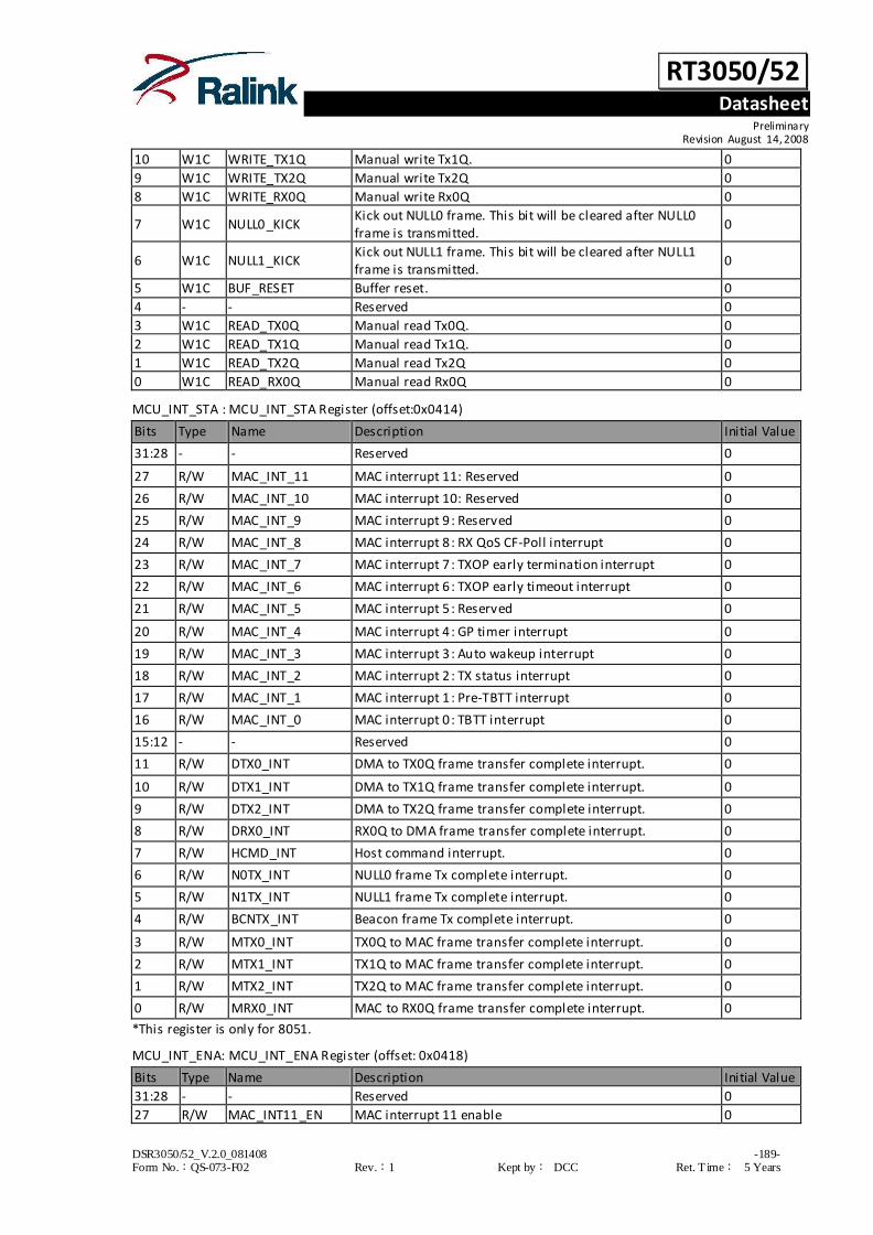
RT3050/52 Datasheet
Preliminary Revision August 14, 2008
DSR3050/52_V.2.0_081408 -189- Form No.:QS-073-F02 Rev.:1 Kept by: DCC Ret. T ime: 5 Years
10 W1C WRITE_TX1Q Manual write Tx1Q. 0
9 W1C WRITE_TX2Q Manual write Tx2Q 0
8 W1C WRITE_RX0Q Manual write Rx0Q 0
7 W1C NULL0_KICK Kick out NULL0 frame. This bit will be cleared after NULL0 frame is transmitted.
0
6 W1C NULL1_KICK Kick out NULL1 frame. This bit will be cleared after NULL1 frame is transmitted.
0
5 W1C BUF_RESET Buffer reset. 0
4 - - Reserved 0
3 W1C READ_TX0Q Manual read Tx0Q. 0
2 W1C READ_TX1Q Manual read Tx1Q. 0
1 W1C READ_TX2Q Manual read Tx2Q 0
0 W1C READ_RX0Q Manual read Rx0Q 0
MCU_INT_STA : MCU_INT_STA Register (offset:0x0414)
Bits Type Name Description Initial Value
31:28 - - Reserved 0
27 R/W MAC_INT_11 MAC interrupt 11: Reserved 0
26 R/W MAC_INT_10 MAC interrupt 10: Reserved 0
25 R/W MAC_INT_9 MAC interrupt 9 : Reserved 0
24 R/W MAC_INT_8 MAC interrupt 8 : RX QoS CF-Poll interrupt 0
23 R/W MAC_INT_7 MAC interrupt 7 : TXOP early termination interrupt 0
22 R/W MAC_INT_6 MAC interrupt 6 : TXOP early timeout interrupt 0
21 R/W MAC_INT_5 MAC interrupt 5 : Reserved 0
20 R/W MAC_INT_4 MAC interrupt 4 : GP timer interrupt 0
19 R/W MAC_INT_3 MAC interrupt 3 : Auto wakeup interrupt 0
18 R/W MAC_INT_2 MAC interrupt 2 : TX status interrupt 0
17 R/W MAC_INT_1 MAC interrupt 1 : Pre-TBTT interrupt 0
16 R/W MAC_INT_0 MAC interrupt 0 : TBTT interrupt 0
15:12 - - Reserved 0
11 R/W DTX0_INT DMA to TX0Q frame transfer complete interrupt. 0
10 R/W DTX1_INT DMA to TX1Q frame transfer complete interrupt. 0
9 R/W DTX2_INT DMA to TX2Q frame transfer complete interrupt. 0
8 R/W DRX0_INT RX0Q to DMA frame transfer complete interrupt. 0
7 R/W HCMD_INT Host command interrupt. 0
6 R/W N0TX_INT NULL0 frame Tx complete interrupt. 0
5 R/W N1TX_INT NULL1 frame Tx complete interrupt. 0
4 R/W BCNTX_INT Beacon frame Tx complete interrupt. 0
3 R/W MTX0_INT TX0Q to MAC frame transfer complete interrupt. 0
2 R/W MTX1_INT TX1Q to MAC frame transfer complete interrupt. 0
1 R/W MTX2_INT TX2Q to MAC frame transfer complete interrupt. 0
0 R/W MRX0_INT MAC to RX0Q frame transfer complete interrupt. 0
*This register is only for 8051.
MCU_INT_ENA: MCU_INT_ENA Register (offset: 0x0418)
Bits Type Name Description Initial Value
31:28 - - Reserved 0
27 R/W MAC_INT11_EN MAC interrupt 11 enable 0

RT3050/52 Datasheet
Preliminary Revision August 14, 2008
DSR3050/52_V.2.0_081408 -190- Form No.:QS-073-F02 Rev.:1 Kept by: DCC Ret. T ime: 5 Years
26 R/W MAC_INT10_EN MAC interrupt 10 enable 0
25 R/W MAC_INT9_EN MAC interrupt 9 enable 0
24 R/W MAC_INT8_EN MAC interrupt 8 enable 0
23 R/W MAC_INT7_EN MAC interrupt 7 enable 0
22 R/W MAC_INT6_EN MAC interrupt 6 enable 0
21 R/W MAC_INT5_EN MAC interrupt 5 enable 0
20 R/W MAC_INT4_EN MAC interrupt 4 enable 0
19 R/W MAC_INT3_EN MAC interrupt 3 enable 0
18 R/W MAC_INT2_EN MAC interrupt 2 enable 0 17 R/W MAC_INT1_EN MAC interrupt 1 enable 0
16 R/W MAC_INT0_EN MAC interrupt 0 enable 0
15:12 - - Reserved 0
11 R/W DTX0_INT_EN DMA to TX0Q frame transfer complete interrupt enable. 0
10 R/W DTX1_INT_EN DMA to TX1Q frame transfer complete interrupt enable. 0
9 R/W DTX2_INT_EN DMA to TX2Q frame transfer complete interrupt enable. 0
8 R/W DRX0_INT_EN RX0Q to DMA frame transfer complete interrupt enable. 0
7 R/W HCMD_INT_EN Host command interrupt enable. 0
6 R/W N0TX_INT_EN NULL0 frame Tx complete interrupt enable. 0
5 R/W N1TX_INT_EN NULL1 frame Tx complete interrupt enable. 0
4 R/W BCNTX_INT_EN Beacon frame Tx complete interrupt enable. 0
3 R/W MTX0_INT_EN TX0Q to MAC frame transfer complete interrupt enable. 0
2 R/W MTX1_INT_EN TX1Q to MAC frame transfer complete interrupt enable. 0
1 R/W MTX2_INT_EN TX2Q to MAC frame transfer complete interrupt enable. 0
0 R/W MRX0_INT_EN MAC to RX0Q frame transfer complete interrupt enable. 0
*This register is only for 8051.
TX0Q_IO: TX0Q_IO Register (offset: 0x041C)
Bits Type Name Description Initial Value
31:16 - - Reserved 0
15:0 R/W TX0Q_IO TX0Q IO port. This register is used in manual mode. 0
TX1Q_IO: TX1Q_IO Register (offset: 0x0420)
Bits Type Name Description Initial Value
31:16 - - Reserved 0
15:0 R/W TX1Q_IO TX1Q IO port. This register is used in manual mode. 0
TX2Q_IO: TX2Q_IO Register (offset: 0x0424)
Bits Type Name Description Initial Value
31:16 - - Reserved 0
15:0 R/W TX2Q_IO TX2Q IO port. This register is used in manual mode. 0
RX0Q_IO: RX0Q_IO Register (offset: 0x0428)
Bits Type Name Description Initial Value
31:16 - - Reserved 0
15:0 R/W RX0Q_IO RX0Q IO port. This register is used in manual mode. 0
BCN_OFFSET0: BCN_OFFSET0 Register (offset: 0x042C)
Bits Type Name Description Initial Value
31:24 R/W BCN3_OFFSET Beacon #3 address offset in shared memory. Unit is 64 byte. 8’hec 23:16 R/W BCN2_OFFSET Beacon #2 address offset in shared memory. Unit is 64 byte. 8’he8
15:8 R/W BCN1_OFFSET Beacon #1 address offset in shared memory. Unit is 64 byte. 8’he4
7:0 R/W BCN0_OFFSET Beacon #0 address offset in shared memory. Unit is 64 byte. 8’he0
BCN_OFFSET1: BCN_OFFSET1 Register (offset: 0x0430)
Bits Type Name Description Initial Value
31:24 R/W BCN7_OFFSET Beacon #7 address offset in shared memory. Unit is 64 byte. 8’hfc

RT3050/52 Datasheet
Preliminary Revision August 14, 2008
DSR3050/52_V.2.0_081408 -191- Form No.:QS-073-F02 Rev.:1 Kept by: DCC Ret. T ime: 5 Years
23:16 R/W BCN6_OFFSET Beacon #6 address offset in shared memory. Unit is 64 byte. 8’hf8
15:8 R/W BCN5_OFFSET Beacon #5 address offset in shared memory. Unit is 64 byte. 8’hf4
7:0 R/W BCN4_OFFSET Beacon #4 address offset in shared memory. Unit is 64 byte. 8’hf0
TXRXQ_STA: TXRXQ_STA Register (offset: 0x0434)
Bits Type Name Description Initial Value
31:24 RO RX0Q_STA RxQ status 8’h22
23:16 RO TX2Q_STA Tx2Q status 8’h02
15:8 RO TX1Q_STA Tx1Q status 8’h02
7:0 RO TX0Q_STA Tx0Q status 8’h02
TXRXQ_PCNT: TXRXQ_PCNT Register (offset: 0x0438)
Bits Type Name Description Initial Value
31:24 RO RX0Q_PCNT Page count in RxQ 8’h00
23:16 RO TX2Q_PCNT Page count in Tx2Q 8’h00
15:8 RO TX1Q_PCNT Page count in Tx1Q 8’h00
7:0 RO TX0Q_PCNT Page count in Tx0Q 8’h00
PBF_DBG: PBF_DBG Register (offset: 0x043C)
Bits Type Name Description Initial Value
31:8 - - Reserved 0
7:0 RO FREE_PCNT Free page count 8’hFE
CAP_CTRL: CAP_CTRL Register (offset: 0x0440)
Bits Type Name Description Initial Value
31 R/W CAP_ADC_FEQ Data source. 0: data from the ADC output
1: Data from the FEQ output
0
30 WC CAP_START
Data capture start 0: No action 1: Start data capture (cleared automatically after capture finished)
0
29 W1C MAN_TRIG Manual capture trigger 0
28:16 R/W TRIG_OFFSET Starting address offset before trigger point. 13’h140
15:13 - - Reserved 0
12:0 RO START_ADDR Starting address of captured data. 13’h000
3.20.3.3 Register Description – RF CFG (base: 1018.0000)
RF_CSR_CFG: RF_CSR_CFG Register (offset: 0x0500)
Bits Type Name Description Init Value
31:18 R - Reserved 0 17 R/W1 RF_CSR_KICK Write – kick RF register read/write
0: do nothing 1: kick read/write process
Read – Polling RF register read/write 0: idle 1: busy
0
16 R/W RF_CSR_WR 0: read 1: write 0
15:13 R Reserved 0
12:8 R/W TESTCSR_RFACC_REGNUM
RF register ID 0 for R0, 1 for R1 and so on.
0
7:0 R/W RF_CSR_DATA Write – DATA written to RF Read – DATA read from RF
0
RF_SETTING: RF_SETTING Register (offset: 0x0504)
Bits Type Name Description Init Value
31:26 R - Reserved 0

RT3050/52 Datasheet
Preliminary Revision August 14, 2008
DSR3050/52_V.2.0_081408 -192- Form No.:QS-073-F02 Rev.:1 Kept by: DCC Ret. T ime: 5 Years
25 R/W TEST_RF_PA_PE_G1 RF_PA_PE_G0 value for Rx path 1 in test mode 0
24 R/W TEST_RF_DC_CAL_EN1 RF_DC_CAL_EN value for Rx path 1 in test mode 0
23 R - Reserved
22:21 R/W TEST_RF_LNA1 RF_LNA value for Rx path 1 in test mode 0
20:16 R/W TEST_RF_VGA1 RF VGA value for Rx path 1 in test mode 0
15:13 R - Reserved
12 R/W TESTCSR_RF_PE RF_PE value in test mode 0
11 R/W TESTCSR_RF_TR RF_TR value in test mode 0
10 R/W TEST_RF_LDO123_PE LDO123_PE value in test mode 0 9 R/W TEST_RF_PA_PE_G0 RF_PA_PE_G0 value for Rx path 0 in test mode 0
8 R/W TEST_RF_DC_CAL_EN0 RF_DC_CAL_EN value for Rx path 0 in test mode 0
7 R - Reserved
6:5 R/W TEST_RF_LNA0 RF_LNA value for Rx path 0 in test mode 0
4:0 R/W TEST_RF_VGA0 RF VGA value for Rx path 0 in test mode 0
RF_TEST_CONTROL: RF_TEST_CONTROL Register (offset: 0x0508)
Bits Type Name Description Init Value
31:1 R - Reserved 0
0 R/W BYPASS_RF When set, RF control signals come from RF_SETTING
instead of MAC/BBP in normal operation mode
0
3.20.3.4 Register Description - MAC (base: 1018.0000)
ASIC_VER_ID: ASIC_VER_ID Register (offset: 0x1000)
Bits Type Name Description Initial value
31:16 R VER_ID ASIC version ID 16’h2860
15:0 R REV_ID ASIC reversion ID 16’h0101
MAC_SYS_CTRL: MAC_SYS_CTRL Register (offset: 0x1004)
Bits Type Name Description Initial value
31:8 - - Reserved 0
7 R/W RX_TS_EN
Write 32-bit hardware RX timestamp instead of (RXWI->RSSI), and write (RXWI->RSSI) instead of (RXWI->SNR).
Note: For QA RX sniffer mode only.
1: enable
0: disable
0
6 R/W WLAN_HALT_EN
Enable external WLAN halt control signal
1: enable
0: disable
0
5 R/W PBF_LOOP_EN
Packet buffer loop back enable (TX->RX)
1: enable
0: disable
0
4 R/W CONT_TX_TEST
Continuous TX production test; override MAC_RX_EN, MAC_TX_EN
1: enable
0: disable
0
3 R/W MAC_RX_EN
MAC RX enable
1: enable
0: disable
0
2 R/W MAC_TX_EN MAC TX enable 0

RT3050/52 Datasheet
Preliminary Revision August 14, 2008
DSR3050/52_V.2.0_081408 -193- Form No.:QS-073-F02 Rev.:1 Kept by: DCC Ret. T ime: 5 Years
1: enable
0: disable
1 R/W BBP_HRST
BBP hard-reset
1: BBP in reset state
0: BBP in normal state
Note: Whole BBP including BBP registers will be reset.
1
0 R/W MAC_SRST
MAC soft-reset
1: MAC in reset state
0: MAC in normal state
Note: MAC registers and tables will NOT be reset.
1
Note: MAC hard-reset is outside the scope of MAC registers.
MAC_ADDR_DW0: MAC_ADDR_DW0 Register (offset: 0x1008)
Bits Type Name Description Initial value
31:24 R/W MAC_ADDR_3 MAC address byte3 0
23:16 R/W MAC_ADDR_2 MAC address byte2 0
15:8 R/W MAC_ADDR_1 MAC address byte1 0
7:0 R/W MAC_ADDR_0 MAC address byte0 0
MAC_ADDR_DW1: MAC_ADDR_DW1 Register (offset: 0x100C)
Bits Type Name Description Initial value
31:16 - - Reserved 0
15:8 R/W MAC_ADDR_5 MAC address byte5 0
7:0 R/W MAC_ADDR_4 MAC address byte4 0
Note: Byte0 is the first byte on network. Its LSB bit is the first bit on network. For a MAC address captured on the
network with order 00:01:02:03:04:05, byte0=00, byte1=01 etc.
MAC_BSSID_DW0: MAC_BSSID_DW0 Register (offset: 0x1010)
Bits Type Name Description Initial value
31:24 R/W BSSID_3 BSSID byte3 0
23:16 R/W BSSID_2 BSSID byte2 0
15:8 R/W BSSID_1 BSSID byte1 0
7:0 R/W BSSID_0 BSSID byte0 0
MAC_BSSID_DW1: MAC_BSSID_DW1 Register (offset: 0x1014)
Bits Type Name Description Initial value
31:21 - - Reserved 0
20:18 R/W MULTI_BCN_NUM
Multiple BSSID Beacon number
0: one back-off beacon
1-7: SIFS-burst beacon count
0
17:16 R/W MULTI_BSSID_MODE
Multiple BSSID mode
In multiple-BSSID AP mode, BSSID shall be the same as MAC_ADDR, that is, this device owns multiple MAC_ADDR in this mode.
The multiple MAC_ADDR/BSSID are distinguished by [bit2: bit0] of byte5.
0

RT3050/52 Datasheet
Preliminary Revision August 14, 2008
DSR3050/52_V.2.0_081408 -194- Form No.:QS-073-F02 Rev.:1 Kept by: DCC Ret. T ime: 5 Years
0: 1-BSSID mode (BSS index = 0)
1: 2-BSSID mode (byte5.bit0 as BSS index)
2: 4-BSSID mode (byte5.bit1:0 as BSS index)
3: 8-BSSID mode (byte5.bit2:0 as BSS index)
15:8 R/W BSSID_5 BSSID byte5 0
7:0 R/W BSSID_4 BSSID byte4 0
MAX_LEN_CFG: MAX_LEN_CFG Register (offset: 0x1018)
Bits Type Name Description Initial value
31:20 - - Reserved 0
19:16 R/W MIN_MPDU_LEN Minimum MPDU length (unit: bytes)
MAC will drop the MPDU if the length is less than this limitation. Applied only in MAC RX.
10
15:14 - - Reserved 0
13:12 R/W MAX_PSDU_LEN Maximum PSDU length (power factor)
0: 2^13 = 8K bytes
1: 2^14 = 16K bytes
2: 2^15 = 32K bytes
3: 2^16 = 64K bytes
MAC will NOT generate A-MPDU with length greater than this limitation. Applied only in MAC TX.
0
11:0 R/W MAX_MPDU_LEN Maximum MPDU length (unit: bytes)
MAC will drop the MPDU if the length is greater than this limitation. Applied only in MAC RX.
4095
BBP_CSR_CFG: BBP_CSR_CFG Register (offset: 0x101C)
Bits Type Name Description Initial value
31:20 - - Reserved 0
19 R/W BBP_RW_MODE
BBP Register R/W mode
1: parallel mode
0: serial mode
1
18 R/W BBP_PAR_DUR
BBP Register parallel R/W pulse width
0: pulse width = 62.5ns
1: pulse width = 112.5ns
Note: Please set BBP_PAR_DUR=1 in 802.11J mode.
0
17 R/W BBP_CSR_KICK
Write - kick BBP register read/write
0: do nothing 1: kick read/write process
Read - Polling BBP register read/write progress
0: idle, 1: busy
0
16 R/W BBP_CSR_RW 0: Write
1: Read 0
15:8 R/W BBP_ADDR BBP register ID
0 for R0, 1 for R1, and so on. 0
7:0 R/W BBP_DATA Write - Data written to BBP
Read - Data read from BBP 0

RT3050/52 Datasheet
Preliminary Revision August 14, 2008
DSR3050/52_V.2.0_081408 -195- Form No.:QS-073-F02 Rev.:1 Kept by: DCC Ret. T ime: 5 Years
RF_CSR_CFG0: RF_CSR_CFG0 Register (offset: 0x1020)
Bits Type Name Description Initial value
31 R/W RF_REG_CTRL Write: 1 - RF_REG0/1/2 to RF chip
Read: 0 – idle, 1 - busy 0
30 R/W RF_LE_SEL
RF_LE selection
0:RF_LE0 activate
1:RF_LE1 activate
0
29 R/W RF_LE_STBY
RF_LE standby mode
0: RF_LE is high when standby
1: RF_LE is low when standby
0
28:24 R/W RF_REG_WIDTH RF register bit width
Default: 22 22
23:0 R/W RF_REG_0 RF register0 ID and content 0
RF_CSR_CFG1: RF_CSR_CFG1 Register (offset: 0x1024)
Bits Type Name Description Initial value
31:25 - - Reserved 0
24 R/W RF_DUR
Gap between BB_CONTROL_RF and RF_LE
0: 3 system clock cycle (37.5usec)
1: 5 system clock cycle (62.5usec)
0
23:0 R/W RF_REG_1 RF register1 ID and content 0
RF_CSR_CFG2: RF_CSR_CFG2 Register (offset: 0x1028)
Bits Type Name Description Initial value
31:24 - - Reserved 0
23:0 R/W RF_REG_2 RF register2 ID and content 0
Note: Software should make sure the first bit (MSB in the specified bit number) written to RF is 0 for RF chip
mode selection)
LED_CFG: LED_CFG Register (offset: 0x102C)
Bits Type Name Description Initial value
31 - - Reserved 0
30 R/W LED_POL
LED polarity
0: active low
1: active high
0
29:28 R/W Y_LED_MODE
Yellow LED mode
0: off
1: blinking upon TX
2: periodic slow blinking
3: always on
0
27:26 R/W G_LED_MODE
Green LED mode
0: off
1: blinking upon TX
2: periodic slow blinking
3: always on
2
25:24 R/W R_LED_MODE
Red LED mode
0: off
1: blinking upon TX
1

RT3050/52 Datasheet
Preliminary Revision August 14, 2008
DSR3050/52_V.2.0_081408 -196- Form No.:QS-073-F02 Rev.:1 Kept by: DCC Ret. T ime: 5 Years
2: periodic slow blinking
3: always on
23:22 - - Reserved 0
21:16 R/W SLOW_BLK_TIME Slow blinking period (unit: 1sec) 3
15:8 R/W LED_OFF_TIME TX blinking off period (unit: 1ms) 30
7:0 R/W LED_ON_TIME TX blinking on period (unit: 1ms) 70
AMPDU_MAX_LEN_20M1S: AMPDU_MAX_LEN_20M1S Register (offset: 0x1030)
Bits Type Name Description Initial value
31:28 R/W AMPDU_MAX_BW20_MCS7 Maximum AMPDU for BW20 MCS7* 7
27:24 R/W AMPDU_MAX_BW20_MCS6 Maximum AMPDU for BW20 MCS6* 7
23:20 R/W AMPDU_MAX_BW20_MCS5 Maximum AMPDU for BW20 MCS5* 7
19:16 R/W AMPDU_MAX_BW20_MCS4 Maximum AMPDU for BW20 MCS4* 7
15:12 R/W AMPDU_MAX_BW20_MCS3 Maximum AMPDU for BW20 MCS3* 7
11:08 R/W AMPDU_MAX_BW20_MCS2 Maximum AMPDU for BW20 MCS2* 7
07:04 R/W AMPDU_MAX_BW20_MCS1 Maximum AMPDU for BW20 MCS1* 7
03:00 R/W AMPDU_MAX_BW20_MCS0 Maximum AMPDU for BW20 MCS0* 7
Note1*: 0-2: 2K bytes, 3: 4K bytes, 4: 8K, 5: 16K, 6: 32K, 7: 64K
Note2: The value applied together with 0x1018 MAX_PSDU_LEN.
AMPDU_MAX_LEN_20M2S: AMPDU_MAX_LEN_20M2S Register (offset: 0x1034)
Bits Type Name Description Initial value
31:28 R/W AMPDU_MAX_BW20_MCS15 Maximum AMPDU for BW20 MCS15* 7
27:24 R/W AMPDU_MAX_BW20_MCS14 Maximum AMPDU for BW20 MCS14* 7
23:20 R/W AMPDU_MAX_BW20_MCS13 Maximum AMPDU for BW20 MCS13* 7
19:16 R/W AMPDU_MAX_BW20_MCS12 Maximum AMPDU for BW20 MCS12* 7
15:12 R/W AMPDU_MAX_BW20_MCS11 Maximum AMPDU for BW20 MCS11* 7
11:08 R/W AMPDU_MAX_BW20_MCS10 Maximum AMPDU for BW20 MCS10* 7
07:04 R/W AMPDU_MAX_BW20_MCS9 Maximum AMPDU for BW20 MCS9* 7
03:00 R/W AMPDU_MAX_BW20_MCS8 Maximum AMPDU for BW20 MCS8* 7
Note1*: 0-2: 2K bytes, 3: 4K bytes, 4: 8K, 5: 16K, 6: 32K, 7: 64K
Note2: The value applied together with 0x1018 MAX_PSDU_LEN.
AMPDU_MAX_LEN_40M1S: AMPDU_MAX_LEN_40M1S Register (offset: 0x1038)
Bits Type Name Description Initial value
31:28 R/W AMPDU_MAX_BW40_MCS7 Maximum AMPDU for BW40 MCS7* 7
27:24 R/W AMPDU_MAX_BW40_MCS6 Maximum AMPDU for BW40 MCS6* 7
23:20 R/W AMPDU_MAX_BW40_MCS5 Maximum AMPDU for BW40 MCS5* 7
19:16 R/W AMPDU_MAX_BW40_MCS4 Maximum AMPDU for BW40 MCS4* 7
15:12 R/W AMPDU_MAX_BW40_MCS3 Maximum AMPDU for BW40 MCS3* 7
11:08 R/W AMPDU_MAX_BW40_MCS2 Maximum AMPDU for BW40 MCS2* 7
07:04 R/W AMPDU_MAX_BW40_MCS1 Maximum AMPDU for BW40 MCS1* 7
03:00 R/W AMPDU_MAX_BW40_MCS0 Maximum AMPDU for BW40 MCS0* 7
Note1*: 0-2: 2K bytes, 3: 4K bytes, 4: 8K, 5: 16K, 6: 32K, 7: 64K
Note2: The value applied together with 0x1018 MAX_PSDU_LEN.
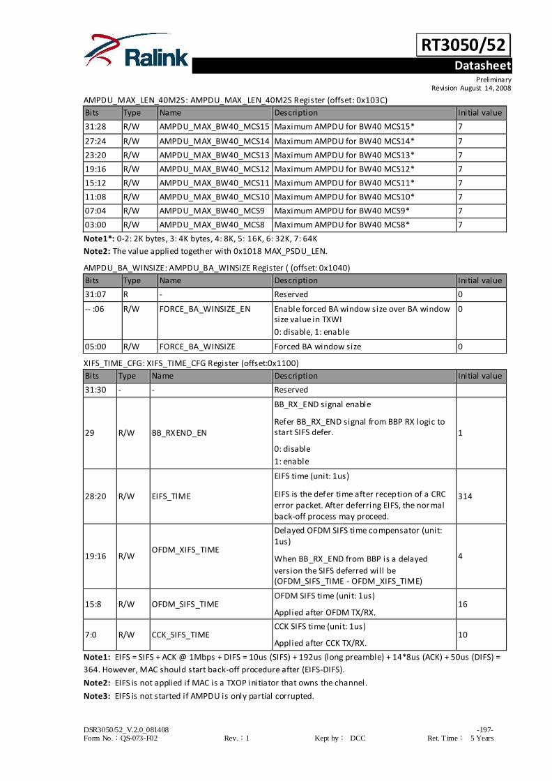
RT3050/52 Datasheet
Preliminary Revision August 14, 2008
DSR3050/52_V.2.0_081408 -197- Form No.:QS-073-F02 Rev.:1 Kept by: DCC Ret. T ime: 5 Years
AMPDU_MAX_LEN_40M2S: AMPDU_MAX_LEN_40M2S Register (offset: 0x103C)
Bits Type Name Description Initial value
31:28 R/W AMPDU_MAX_BW40_MCS15 Maximum AMPDU for BW40 MCS15* 7
27:24 R/W AMPDU_MAX_BW40_MCS14 Maximum AMPDU for BW40 MCS14* 7
23:20 R/W AMPDU_MAX_BW40_MCS13 Maximum AMPDU for BW40 MCS13* 7
19:16 R/W AMPDU_MAX_BW40_MCS12 Maximum AMPDU for BW40 MCS12* 7
15:12 R/W AMPDU_MAX_BW40_MCS11 Maximum AMPDU for BW40 MCS11* 7
11:08 R/W AMPDU_MAX_BW40_MCS10 Maximum AMPDU for BW40 MCS10* 7
07:04 R/W AMPDU_MAX_BW40_MCS9 Maximum AMPDU for BW40 MCS9* 7
03:00 R/W AMPDU_MAX_BW40_MCS8 Maximum AMPDU for BW40 MCS8* 7
Note1*: 0-2: 2K bytes, 3: 4K bytes, 4: 8K, 5: 16K, 6: 32K, 7: 64K
Note2: The value applied together with 0x1018 MAX_PSDU_LEN.
AMPDU_BA_WINSIZE: AMPDU_BA_WINSIZE Register ( (offset: 0x1040)
Bits Type Name Description Initial value
31:07 R - Reserved 0
-- :06 R/W FORCE_BA_WINSIZE_EN Enable forced BA window size over BA window size value in TXWI
0: disable, 1: enable
0
05:00 R/W FORCE_BA_WINSIZE Forced BA window size 0
XIFS_TIME_CFG: XIFS_TIME_CFG Register (offset:0x1100)
Bits Type Name Description Initial value
31:30 - - Reserved
29 R/W BB_RXEND_EN
BB_RX_END signal enable
Refer BB_RX_END signal from BBP RX logic to start SIFS defer.
0: disable
1: enable
1
28:20 R/W EIFS_TIME
EIFS time (unit: 1us)
EIFS is the defer time after reception of a CRC error packet. After deferring EIFS, the normal back-off process may proceed.
314
19:16 R/W OFDM_XIFS_TIME
Delayed OFDM SIFS time compensator (unit: 1us)
When BB_RX_END from BBP is a delayed
version the SIFS deferred will be (OFDM_SIFS_TIME - OFDM_XIFS_TIME)
4
15:8 R/W OFDM_SIFS_TIME OFDM SIFS time (unit: 1us)
Applied after OFDM TX/RX. 16
7:0 R/W CCK_SIFS_TIME CCK SIFS time (unit: 1us)
Applied after CCK TX/RX. 10
Note1: EIFS = SIFS + ACK @ 1Mbps + DIFS = 10us (SIFS) + 192us (long preamble) + 14*8us (ACK) + 50us (DIFS) =
364. However, MAC should start back-off procedure after (EIFS-DIFS).
Note2: EIFS is not applied if MAC is a TXOP i nitiator that owns the channel.
Note3: EIFS is not started if AMPDU is only partial corrupted.

RT3050/52 Datasheet
Preliminary Revision August 14, 2008
DSR3050/52_V.2.0_081408 -198- Form No.:QS-073-F02 Rev.:1 Kept by: DCC Ret. T ime: 5 Years
Caution: It is recommended that both (CCK_SIFS_TIME) and (OFDM_SIFS_TIME) are no less than TX/RX transition
time. If the SIFS value is not long enough, a SIFS burst transmission may be replaced with a PIFS burst one.
BKOFF_SLOT_CFG: BKOFF_SLOT_CFG Register (offset: 0x1104)
Bits Type Name Description Initial value
31:12 - - Reserved 0
11:8 R/W CC_DELAY_TIME
Channel clear delay (unit: 1-us)
This value specified the TX guard time after channel is clear.
2
7:0 R/W SLOT_TIME
Slot time (unit: 1-us)
This value specified the slot boundary after deferring SIFS time.
Note: Default 20us is for 11b/g. 11a and 11g-short-slot-mode is 9us.
20
NAV_TIME_CFG: NAV_TIME_CFG Register (offset: 0x1108)
Bits Type Name Description Initial value
31 WC NAV_UPD
NAV timer manual update command
0: Do nothing
1: Update NAV timer with NAV_UPD_VAL
0
30:16 R/W NAV_UPD_VAL NAV timer manual update value (unit: 1us) 0
15 R/W NAV_CLR_EN
NAV timer auto-clear enable
When enabled, MAC will auto clear NAV timer after the reception of CF-End frame from previous NAV holder STA.
0: disable
1: enable
1
14:0 R NAV_TIMER
NAV timer (unit: 1us)
The timer is set by other STA and will auto countdown to zero. The STA who set the NAV timer is called the NAV holder. When NAV timer is nonzero, MAC will not send any packet.
0
CH_TIME_CFG: CH_TIME_CFG Register (offset: 0x110C)
Bits Type Name Description Initial value
31:5 - - Reserved 0
4 R/W EIFS_AS_CH_BUSY
Count EIFS as channel busy
0: disable
1: enable
1
3 R/W NAV_AS_CH_BUSY
Count NAV as channel busy
0: disable
1: enable
1
2 R/W RX_AS_CH_BUSY
Count RX busy as channel busy
0: disable
1: enable
1
1 R/W TX_AS_CH_BUSY
Count TX busy as channel busy
0: disable
1: enable
1

RT3050/52 Datasheet
Preliminary Revision August 14, 2008
DSR3050/52_V.2.0_081408 -199- Form No.:QS-073-F02 Rev.:1 Kept by: DCC Ret. T ime: 5 Years
0 R/W CH_STA_TIMER_EN
Channel statistic timer enable
0: disable
1: enable
0
PBF_LIFE_TIMER: PBF_LIFE_TIMER Register (offset: 0x1110)
Bits Type Name Description Initial value
31:0 R PBF_LIFE_TIMER TX/RX MPDU timestamp timer (free run)
Unit: 1us 0
BCN_TIME_CFG: BCN_TIME_CFG Register (offset: 0x1114)
Bits Type Name Description Initial value
31:24 R/W TSF_INS_COMP
TSF insertion compensation value (unit: 1us)
When inserting TSF, add this value with local TSF timer as the TX timestamp.
0
23:21 - - Reserved 0
20 R/W BCN_TX_EN
BEACON frame TX enable
When enabled, MAC sends BEACON frame at TBTT interrupt.
0: disable
1: enable
0
19 R/W TBTT_TIMER_EN
TBTT timer enable
When enabled, TBTT interrupt will be issued periodically with period specified in (BCN_INTVAL).
0: disable
1: enable
0
18:17 R/W TSF_SYNC_MODE
Local 64-bit TSF timer synchronization mode
00: disable
01: (STA infra-structure mode) Upon the reception of
BEACON frame from associated BSS, local TSF is always updated with remote TSF.
10: (STA ad-hoc mode) Upon the reception of BEACON frame from associated BSS, local TSF is updated with remote TSF only if the remote TSF is greater than local TSF.
11: (AP mode) SYNC with nobody
0
16 R/W TSF_TIMER_EN
Local 64-bit TSF timer enable
When enabled, TSF timer will re-start from zero.
0: disable
1: enable
0
15:0 R/W BCN_INTVAL
BEACON interval (unit: 64us)
This value specified the interval between
Maximum beacon interval is about 4sec.
1600
TBTT_SYNC_CFG: TBTT_SYNC_CFG Register (offset: 0x1118)
Bits Type Name Description Initial value
31:24 - - Reserved 0
23:20 R/W BCN_CWMIN Beacon transmission CWMIN after TBTT interrupt (unit: 4

RT3050/52 Datasheet
Preliminary Revision August 14, 2008
DSR3050/52_V.2.0_081408 -200- Form No.:QS-073-F02 Rev.:1 Kept by: DCC Ret. T ime: 5 Years
slot)
19:16 R/W BCN_AIFSN Beacon transmission AIFSN after TBTT interrupt (unit: slot)
2
15:8 R/W BCN_EXP_WIN
Beacon expecting window duration (unit: 64us)
The window starts from TBTT interrupt. The phase of “TBTT interrupt train” will NOT be adjusted by the beacon arrived within the window.
32
7:0 R/W TBTT_ADJUST
IBSS mode TBTT phase adaptive adjustment step (unit: 1us), default value is 16us.
In IBSS mode (Ad hoc), if consecutive TX beacon failures
(or consecutive success) happened, TBTT timer will adjust it phase to meet the external Ad hoc TBTT time.
16
TSF_TIMER_DW0: TSF_TIMER_DW0 Register (offset: 0x111C)
Bits Type Name Description Initial value
31:0 R TSF_TIMER_DW0 Local TSF timer LSB 32 bits (unit: 1us) 0
TSF_TIMER_DW1: TSF_TIMER_DW1 Register (offset: 0x1120)
Bits Type Name Description Initial value
31:0 R TSF_TIMER_DW1 Local TSF timer MSB 32 bits (unit: 1us) 0
TBTT_TIMER: TBTT_TIMER _DW0 Register (offset: 0x1124)
Bits Type Name Description Initial value
31:17 - - Reserved 0
16:0 R TBTT_TIMER
TBTT Timer (unit: 32us)
The time remains till next TBTT.
When TBTT_TIMER_EN is enabled, the timer will down count from BCN_INTVAL to zero.
When TBTT_TIMER_EN is disabled, the timer will stay in zero.
0
INT_TIMER_CFG: INT_TIMER_CFG Register (offset: 0x1128)
Bits Type Name Description Initial value
31:16 R/W GP_TIMER Period of general purpose interrupt timer
(Unit: 64us) 0
15:0 R/W PRE_TBTT_TIMER
Pre-TBTT interrupt time (unit: 64us)
The value specified the interrupt timing before TBTT interrupt.
0
INT_TIMER_EN: INT_TIMER_EN Register (offset: 0x112C)
Bits Type Name Description Initial value
31:2 - - Reserved 0
1 R/W GP_TIMER_EN
Periodic general purpose interrupt timer enable
0: disable
1: enable
0
0 R/W PRE_TBTT_INT_EN
Pre-TBTT interrupt enable
0: disable
1: enable
0

RT3050/52 Datasheet
Preliminary Revision August 14, 2008
DSR3050/52_V.2.0_081408 -201- Form No.:QS-073-F02 Rev.:1 Kept by: DCC Ret. T ime: 5 Years
CH_IDLE_STA: CH_IDLE_STA Register (offset: 0x1130)
Bits Type Name Description Initial value
31:0 RC CH_IDLE_TIME Channel idle time
Unit: 1us 0
In application, the channel busy time can be derived by the equation:
CH_BUSY_TIME = host polling period – CH_IDLE_TIME.
Reserved: Reserved Register (offset: 0x1134)
Bits Type Name Description Initial value
31:0 RC Reserved Reserved 0
MAC_STATUS_REG: MAC_STATUS_REG Register (offset: 0x1200)
Bits Type Name Description Initial value
31:2 - - Reserved 0
1 R RX_STATUS
RX status
0: Idle
1: Busy
0
0 R TX_STATUS
TX status
0: Idle
1: Busy
0
PWR_PIN_CFG: PWR_PIN_CFG Register (offset: 0x1204)
Bits Type Name Description Initial value
31:4 - - Reserved 0
3 R/W IO_ADDA_PD AD/DA power down 0
2 R/W IO_PLL_PD PLL power down 0
1 R/W IO_RA_PE RA_PE 1
0 R/W IO_RF_PE RF_PE 1
AUTO_WAKEUP_CFG: AUTO_WAKEUP _CFG Register (offset:0x1208)
Bits Type Name Description Initial value
31:16 - - Reserved 0
15 R/W AUTO_WAKEUP_EN
Auto wakeup interrupt enable
Auto wakeup interrupt will be issued after #(SLEEP_TBTT_NUM) TBTTs’ at WAKEUP_LEAD_TIME before the target wakeup TBTT.
0: disable
1: enable
Note: Please make sure TBTT_TIMER_EN is enabled.
0
14:8 R/W SLEEP_TBTT_NUM Number of sleeping TBTT 0
7:0 R/W WAKEUP_LEAD_TIME
Auto wakeup lead time (unit: 1TU=1024us) 20
3.20.3.5 MAC TX configuration registers (base: 1018.0000)
EDCA_AC0_CFG (BE): EDCA_AC0_CFG (BE) Register (offset: 0x1300)
Bits Type Name Description Initial value
31:20 - - Reserved 0
19:16 R/W AC0_CWMAX AC0 CWMAX (unit: power of 2) 7
15:12 R/W AC0_CWMIN AC0 CWMIN (unit: power of 2) 3

RT3050/52 Datasheet
Preliminary Revision August 14, 2008
DSR3050/52_V.2.0_081408 -202- Form No.:QS-073-F02 Rev.:1 Kept by: DCC Ret. T ime: 5 Years
11:8 R/W AC0_AIFSN AC0 AIFSN (unit: # of slot time) 2
7:0 R/W AC0_TXOP AC0 TXOP limit (unit: 32us) 0
EDCA_AC1_CFG (BK): EDCA_AC1_CFG (BK) Register (offset: 0x1304)
Bits Type Name Description Initial value
31:20 - - Reserved 0
19:16 R/W AC1_CWMAX AC1 CWMAX (unit: power of 2) 7
15:12 R/W AC1_CWMIN AC1 CWMIN (unit: power of 2) 3
11:8 R/W AC1_AIFSN AC1 AIFSN (unit: # of slot time) 2
7:0 R/W AC1_TXOP AC1 TXOP limit (unit: 32us) 0
EDCA_AC2_CFG (VI): EDCA_AC2_CFG (VI) Register (offset: 0x1308)
Bits Type Name Description Initial value
31:20 - - Reserved 0
19:16 R/W AC2_CWMAX AC2 CWMAX (unit: power of 2) 7
15:12 R/W AC2_CWMIN AC2 CWMIN (unit: power of 2) 3
11:8 R/W AC2_AIFSN AC2 AIFSN (unit: # of slot time) 2
7:0 R/W AC2_TXOP AC2 TXOP limit (unit: 32us) 0
EDCA_AC3_CFG (VO): EDCA_AC3_CFG (VO) Register (offset: 0x130C)
Bits Type Name Description Initial value
31:20 - - Reserved 0
19:16 R/W AC3_CWMAX AC3 CWMAX (unit: power of 2) 7
15:12 R/W AC3_CWMIN AC3 CWMIN (unit: power of 2) 3
11:8 R/W AC3_AIFSN AC3 AIFSN (unit: # of slot time) 2
7:0 R/W AC3_TXOP AC3 TXOP limit (unit: 32us) 0
EDCA_TID_AC_MAP: EDCA_TID_AC_MAP Register (offset: 0x1310)
Bits Type Name Description Initial value
31:16 - - Reserved 0
15:14 R/W TID7_AC_MAP AC value as TID=7 3
13:12 R/W TID6_AC_MAP AC value as TID=6 3
11:10 R/W TID5_AC_MAP AC value as TID=5 2
9:8 R/W TID4_AC_MAP AC value as TID=4 2
7:6 R/W TID3_AC_MAP AC value as TID=3 0
5:4 R/W TID2_AC_MAP AC value as TID=2 1
3:2 R/W TID1_AC_MAP AC value as TID=1 1
1:0 R/W TID0_AC_MAP AC value as TID=0 0
Note: default according 802.11e Table 20.23—User priority to Access Category mappings.
TX_PWR_CFG_0: TX_PWR_CFG_0 Register (offset: 0x1314, default: 0x6666_6666)
Bits Type Name Description Initial value
31:24 R/W TX_PWR_OFDM_12 TX power for OFDM 12M/18M 0x66
23:16 R/W TX_PWR_OFDM_6 TX power for OFDM 6M/9M 0x66
15:8 R/W TX_PWR_CCK_5 TX power for CCK5.5M/11M 0x66
7:0 R/W TX_PWR_CCK_1 TX power for CCK1M/2M 0x66

RT3050/52 Datasheet
Preliminary Revision August 14, 2008
DSR3050/52_V.2.0_081408 -203- Form No.:QS-073-F02 Rev.:1 Kept by: DCC Ret. T ime: 5 Years
TX_PWR_CFG_1: TX_PWR_CFG_1 Register (offset: 0x1318)
Bits Type Name Description Initial value
31:24 R/W TX_PWR_MCS_2 TX power for HT MCS=2,3 0x66
23:16 R/W TX_PWR_MCS_0 TX power for HT MCS=0,1 0x66
15:8 R/W TX_PWR_OFDM_48 TX power for OFDM 48M/54M 0x66
7:0 R/W TX_PWR_OFDM_24 TX power for OFDM 24M/36M 0x66
TX_PWR_CFG_2: TX_PWR_CFG_2 Register (offset: 0x131C)
Bits Type Name Description Initial value
31:24 R/W TX_PWR_MCS_10 TX power for HT MCS=10,11 0x66
23:16 R/W TX_PWR_MCS_8 TX power for HT MCS=8,9 0x66
15:8 R/W TX_PWR_MCS_6 TX power for HT MCS=6,7 0x66
7:0 R/W TX_PWR_MCS_4 TX power for HT MCS=4,5 0x66
TX_PWR_CFG_3: TX_PWR_CFG_3 Register (offset: 0x1320)
Bits Type Name Description Initial value
31:24 R/W - Reserved 0x66
23:16 R/W - Reserved 0x66
15:8 R/W TX_PWR_MCS_14 TX power for HT MCS=14,15 0x66
7:0 R/W TX_PWR_MCS_12 TX power for HT MCS=12,13 0x66
TX_PWR_CFG_4: TX_PWR_CFG_4 Register (offset: 0x1324)
Bits Type Name Description Initial value
31:16 - - Reserved 0
15:8 R/W - Reserved 0x66
7:0 R/W - Reserved 0x66
TX_PIN_CFG: TX_PIN_CFG Register (offset: 0x1328)
Bits Type Name Description Initial value
31:20 - - Reserved 0
19 R/W TRSW_POL TRSW_EN polarity 0
18 R/W TRSW_EN TRSW_EN enable 1
17 R/W RFTR_POL RF_TR polarity 0
16 R/W RFTR_EN RF_TR enable 1
15 R/W LNA_PE_G1_POL LNA_PE_G1 polarity 0
14 R/W LNA_PE_A1_POL LNA_PE_A1 polarity 0
13 R/W LNA_PE_G0_POL LNA_PE_G0 polarity 0
12 R/W LNA_PE_A0_POL LNA_PE_A0 polarity 0
11 R/W LNA_PE_G1_EN LNA_PE_G1 enable 1
10 R/W LNA_PE_A1_EN LNA_PE_A1 enable 1
9 R/W LNA_PE_G0_EN LNA_PE_G0 enable 1
8 R/W LNA_PE_A0_EN LNA_PE_A0 enable 1
7 R/W PA_PE_G1_POL PA_PE_G1 polarity 0
6 R/W PA_PE_A1_POL PA_PE_A1 polarity 0
5 R/W PA_PE_G0_POL PA_PE_G0 polarity 0
4 R/W PA_PE_A0_POL PA_PE_A0 polarity 0
3 R/W PA_PE_G1_EN PA_PE_G1 enable 1

RT3050/52 Datasheet
Preliminary Revision August 14, 2008
DSR3050/52_V.2.0_081408 -204- Form No.:QS-073-F02 Rev.:1 Kept by: DCC Ret. T ime: 5 Years
2 R/W PA_PE_A1_EN PA_PE_A1 enable 1
1 R/W PA_PE_G0_EN PA_PE_G0 enable 1
0 R/W PA_PE_A0_EN PA_PE_A0 enable 1
TX_BAND_CFG: TX_BAND_CFG Register (offset: 0x132C)
Bits Type Name Description Initial value
31:3 - - Reserved 0
2 R/W 5G_BAND_SEL_N 5G band selection PIN (complement of 5G_BAND_SEL_P) 1
1 R/W 5G_BAND_SEL_P 5G band selection PIN 0
0 R/W TX_BAND_SEL 0: use lower 40Mhz band in 20Mhz TX
1: use upper 40Mhz band in 20Mhz TX 0
Note1: TX_BAND_SEL is effective only when TX/RX bandwidth control register R4 of BBP is set to 40Mhz.
TX_SW_CFG0: TX_SW_CFG0 Register (offset: 0x1330)
Bits Type Name Description Initial value
31:24 R/W DLY_RFTR_EN Delay of RF_TR assertion 0x0
23:16 R/W DLY_TRSW_EN Delay of TR_SW assertion 0x4
15:8 R/W DLY_PAPE_EN Delay of PA_PE assertion 0x8
7:0 R/W DLY_TXPE_EN Delay of TX_PE assertion 0xC
Note1: The timing unit is 0.25us.
Note2: SIFS_TIME should compensate with DLY_TXPE_EN.
TX_SW_CFG1: TX_SW_CFG1 Register (offset: 0x1334)
Bits Type Name Description Initial value
31:24 - - Reserved 0
23:16 R/W DLY_RFTR_DIS Delay of RF_TR de-assertion 0xC
15:8 R/W DLY_TRSW_DIS Delay of TR_SW de-assertion 0x8
7:0 R/W DLY_PAPE_DIS Delay of PA_PE de-assertion 0x8
Note1: The timing unit is 0.25us.
Note2: The delay is started from TX_END event of BBP.
Note3: TX_PE is de-asserted automatically as last data byte passed to BBP.
TX_SW_CFG2: TX_SW_CFG2 Register (offset: 0x1338)
Bits Type Name Description Initial value
31:24 R/W DLY_LNA_EN Delay of LNA* assertion 0x0
23:16 R/W DLY_LNA_DIS Delay of LNA* de-assertion 0xC
15:8 R/W DLY_DAC_EN Delay of DAC_PE assertion 0x4
7:0 R/W DLY_DAC_DIS Delay of DAC_PE de-assertion 0x8
Note1: The timing unit is 0.25us.
Note 2: LNA* includes LNA_A0, LNA_A1, LNA_G0, LNA_G1.
TXOP_THRES_CFG: TXOP_THRES_CFG Register (offset: 0x133C)
Bits Type Name Description Initial value
31:24 R/W TXOP_REM_THRES
Remaining TXOP threshold, unit: 32us
As the remaining TXOP is less than the threshold, the TXOP is passed silently.
0
23:16 R/W CF_END_THRES CF-END threshold, unit: 32us
As the remaining TXOP is greater than the threshold, the 0
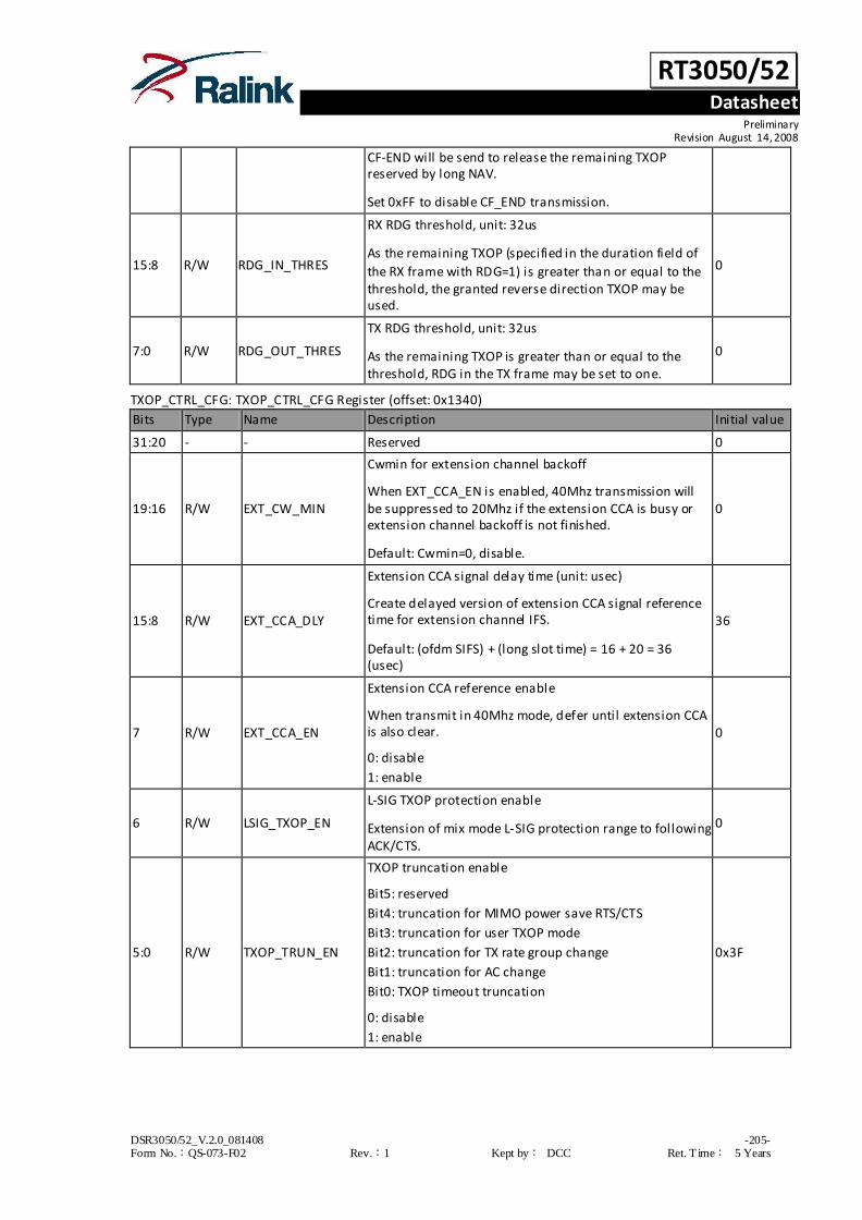
RT3050/52 Datasheet
Preliminary Revision August 14, 2008
DSR3050/52_V.2.0_081408 -205- Form No.:QS-073-F02 Rev.:1 Kept by: DCC Ret. T ime: 5 Years
CF-END will be send to release the remaining TXOP reserved by long NAV.
Set 0xFF to disable CF_END transmission.
15:8 R/W RDG_IN_THRES
RX RDG threshold, unit: 32us
As the remaining TXOP (specified in the duration field of
the RX frame with RDG=1) is greater than or equal to the threshold, the granted reverse direction TXOP may be used.
0
7:0 R/W RDG_OUT_THRES
TX RDG threshold, unit: 32us
As the remaining TXOP is greater than or equal to the threshold, RDG in the TX frame may be set to one.
0
TXOP_CTRL_CFG: TXOP_CTRL_CFG Register (offset: 0x1340)
Bits Type Name Description Initial value
31:20 - - Reserved 0
19:16 R/W EXT_CW_MIN
Cwmin for extension channel backoff
When EXT_CCA_EN is enabled, 40Mhz transmission will be suppressed to 20Mhz if the extension CCA is busy or extension channel backoff is not finished.
Default: Cwmin=0, disable.
0
15:8 R/W EXT_CCA_DLY
Extension CCA signal delay time (unit: usec)
Create delayed version of extension CCA signal reference time for extension channel IFS.
Default: (ofdm SIFS) + (long slot time) = 16 + 20 = 36 (usec)
36
7 R/W EXT_CCA_EN
Extension CCA reference enable
When transmit in 40Mhz mode, defer until extension CCA is also clear.
0: disable
1: enable
0
6 R/W LSIG_TXOP_EN
L-SIG TXOP protection enable
Extension of mix mode L-SIG protection range to following ACK/CTS.
0
5:0 R/W TXOP_TRUN_EN
TXOP truncation enable
Bit5: reserved
Bit4: truncation for MIMO power save RTS/CTS
Bit3: truncation for user TXOP mode
Bit2: truncation for TX rate group change
Bit1: truncation for AC change
Bit0: TXOP timeout truncation
0: disable
1: enable
0x3F

RT3050/52 Datasheet
Preliminary Revision August 14, 2008
DSR3050/52_V.2.0_081408 -206- Form No.:QS-073-F02 Rev.:1 Kept by: DCC Ret. T ime: 5 Years
TX_RTS_CFG: TX_RTS_CFG Register (offset: 0x1344)
Bits Type Name Description Initial value
31:24 - - Reserved 0
24 R/W RTS_FBK_EN RTS rate fallback enable 0
23:8 R/W RTS_THRES
RTS threshold (unit: byte)
MPDU or AMPDU with length greater than RTS threshold will be protected with RTS/CTS exchange at the beginning of the TXOP.
65535
7:0 R/W RTS_RTY_LIMIT Auto RTS retry l imit 7
TX_TIMEOUT_CFG: TX_TIMEOUT_CFG Register (offset: 0x1348)
Bits Type Name Description Initial value
31:24 - - Reserved 0
23:16 R/W TXOP_TIMEOUT
TXOP timeout value for TXOP truncation
Unit: 1usec
Note: It is recommended that (SLOT_TIME) > (TXOP_TIMEOUT) > (RX_ACK_TIMEOUT)
Default: For 20us long slot time.
15
15:8 R/W RX_ACK_TIMEOUT
RX ACK/CTS timeout value for TX procedure
Unit: 1usec
Note: It is recommended that (SLOT_TIME) > (TXOP_TIMEOUT) > (RX_ACK_TIMEOUT)
Default: For 20us long slot time.
10
7:4 R/W MPDU_LIFE_TIME
TX MPDU expiration time
Expiration time = 2^(9+MPDU_LIFE_TIME) us
Default value is 2^(9+9) ~= 256ms
9
3:0 - - Reserved 0
TX_RTY_CFG: TX_RTY_CFG Register (offset: 0x134C)
Bits Type Name Description Initial value
31 - - Reserved 0
30 R/W TX_AUTOFB_EN
TX retry PHY rate auto fallback enable
0: disable
1: enable
0
29 R/W AGG_RTY_MODE
Aggregate MPDU retry mode
0: expired by retry l imit
1: expired by MPDU life timer
1
28 R/W NAG_RTY_MODE
Non-aggregate MPDU retry mode
0: expired by retry l imit
1: expired by MPDU life timer
0
27:16 R/W LONG_RTY_THRES
Long retry threshold
MPDU with length over this threshold is applied with long retry l imit.
3000
15:8 R/W LONG_RTY_LIMIT Long retry l imit 4
7:0 R/W SHORT_RTY_LIMIT Short retry l imit 7
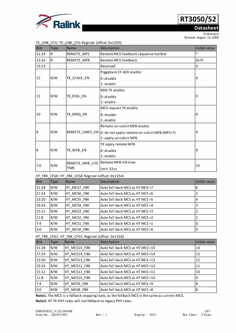
RT3050/52 Datasheet
Preliminary Revision August 14, 2008
DSR3050/52_V.2.0_081408 -207- Form No.:QS-073-F02 Rev.:1 Kept by: DCC Ret. T ime: 5 Years
TX_LINK_CFG: TX_LINK_CFG Register (offset: 0x1350)
Bits Type Name Description Initial value
31:24 R REMOTE_MFS Remote MCS feedback sequence number *
23:16 R REMOTE_MFB Remote MCS feedback 0x7F
15:13 - - Reserved 0
12 R/W TX_CFACK_EN
Piggyback CF-ACK enable
0: disable
1: enable
0
11 R/W TX_RDG_EN
RDG TX enable
0: disable
1: enable
0
10 R/W TX_MRQ_EN
MCS request TX enable
0: disable
1: enable
0
9 R/W REMOTE_UMFS_EN
Remote un-solicit MFB enable
0: do not apply remote un-solicit MFB (MFS=7)
1: apply un-solicit MFB
0
8 R/W TX_MFB_EN
TX apply remote MFB
0: disable
1: enable
0
7:0 R/W REMOTE_MFB_LITETIME
Remote MFB life time
Unit: 32us 32
HT_FBK_CFG0: HT_FBK_CFG0 Register (offset: 0x1354)
Bits Type Name Description Initial value
31:28 R/W HT_MCS7_FBK Auto fall back MCS as HT MCS =7 6
27:24 R/W HT_MCS6 _FBK Auto fall back MCS as HT MCS =6 5
23:20 R/W HT_MCS5_FBK Auto fall back MCS as HT MCS =5 4
19:16 R/W HT_MCS4_FBK Auto fall back MCS as HT MCS =4 3
15:12 R/W HT_MCS3_FBK Auto fall back MCS as HT MCS =3 2
11:8 R/W HT_MCS2_FBK Auto fall back MCS as HT MCS =2 1
7:4 R/W HT_MCS1_FBK Auto fall back MCS as HT MCS =1 0
3:0 R/W HT_MCS0_FBK Auto fall back MCS as HT MCS =0 0
HT_FBK_CFG1: HT_FBK_CFG1 Register (offset: 0x1358)
Bits Type Name Description Initial value
31:28 R/W HT_MCS15_FBK Auto fall back MCS as HT MCS =15 14
27:24 R/W HT_MCS14_FBK Auto fall back MCS as HT MCS =14 13
23:20 R/W HT_MCS13_FBK Auto fall back MCS as HT MCS =13 12
19:16 R/W HT_MCS12_FBK Auto fall back MCS as HT MCS =12 11
15:12 R/W HT_MCS11_FBK Auto fall back MCS as HT MCS =11 10
11:8 R/W HT_MCS10_FBK Auto fall back MCS as HT MCS =10 9
7:4 R/W HT_MCS9_FBK Auto fall back MCS as HT MCS =9 8
3:0 R/W HT_MCS8_FBK Auto fall back MCS as HT MCS =8 8
Note1. The MCS is a fallback stopping state, as the fallback MCS is the same as current MCS.
Note2. HT TX PHY rates will not fallback to legacy PHY rates.

RT3050/52 Datasheet
Preliminary Revision August 14, 2008
DSR3050/52_V.2.0_081408 -208- Form No.:QS-073-F02 Rev.:1 Kept by: DCC Ret. T ime: 5 Years
LG_FBK_CFG0: LG_FBK_CFG0 Register (offset: 0x135C)
Bits Type Name Description Initial value
31:28 R/W OFDM7_FBK Auto fall back MCS as previous TX rate is OFDM 54Mbps. 14
27:24 R/W OFDM6_FBK Auto fall back MCS as previous TX rate is OFDM 48Mbps. 13
23:20 R/W OFDM5_FBK Auto fall back MCS as previous TX rate is OFDM 36Mbps. 12
19:16 R/W OFDM4_FBK Auto fall back MCS as previous TX rate is OFDM 24Mbps. 11
15:12 R/W OFDM3_FBK Auto fall back MCS as previous TX rate is OFDM 18Mbps. 10
11:8 R/W OFDM2_FBK Auto fall back MCS as previous TX rate is OFDM 12Mbps. 9
7:4 R/W OFDM1_FBK Auto fall back MCS as previous TX rate is OFDM 9Mbps. 8
3:0 R/W OFDM0_FBK Auto fall back MCS as previous TX rate is OFDM 6Mbps. 8
LG_FBK_CFG1: LG_FBK_CFG1 Register (offset: 0x1360)
Bits Type Name Description Initial value
31:16 - - Reserved 0
15:12 R/W CCK3_FBK Auto fall back MCS as previous TX rate is CCK 11Mbps. 2
11:8 R/W CCK2_FBK Auto fall back MCS as previous TX rate is CCK 5.5Mbps. 1
7:4 R/W CCK1_FBK Auto fall back MCS as previous TX rate is CCK 2Mbps. 0
3:0 R/W CCK0_FBK Auto fall back MCS as previous TX rate is CCK 1Mbps. 0
Note1. Bit3 of each legacy fallback rate is selection of OFDM/CCK. 0=CCK, 1=OFDM.
CCK_PROT_CFG: CCK_PROT_CFG Register (offset: 0x1364)
Bits Type Name Description Initial value
31:27 - - Reserved 0
26 R/W CCK_RTSTH_EN
RTS threshold enable on CCK TX
0: disable
1: enable
0
25:20 R/W CCK_TXOP_ALLOW
CCK TXOP allowance
(0: disallow, 1: allow)
Bit25: allow GF-40 TX
Bit24: allow GF-20 TX
Bit23: allow MM-40 TX
Bit22: allow MM-20 TX
Bit21: allow OFDM TX
Bit20: allow CCK TX
1
19:18 R/W CCK_PROT_NAV
TXOP protection type for CCK TX
0: None
1: Short NAV protection
2: Long NAV protection
3: Reserved (None)
0
17:16 R/W CCK_PROT_CTRL
Protection control frame type for CCK TX
0: None
1: RTS/CTS
2: CTS-to-self
3: Reserved (None)
0
15:0 R/W CCK_PROT_RATE
Protection control frame rate for CCK TX
(Including RTS/CTS-to-self/CF-END)
Default: CCK 11M
0x0003

RT3050/52 Datasheet
Preliminary Revision August 14, 2008
DSR3050/52_V.2.0_081408 -209- Form No.:QS-073-F02 Rev.:1 Kept by: DCC Ret. T ime: 5 Years
OFDM_PROT_CFG: OFDM_PROT_CFG Register (offset: 0x1368)
Bits Type Name Description Initial value
31:27 - - Reserved 0
26 R/W OFDM_RTSTH_EN
RTS threshold enable on OFDM TX
0: disable
1: enable
0
25:20 R/W OFDM_PROT_TXOP
OFDM TXOP allowance
(0: disallow, 1: allow)
Bit25: allow GF-40 TX
Bit24: allow GF-20 TX
Bit23: allow MM-40 TX
Bit22: allow MM-20 TX
Bit21: allow OFDM TX
Bit20: allow CCK TX
2
19:18 R/W OFDM_PROT_NAV
TXOP protection type for OFDM TX
0: None
1: Short NAV protection
2: Long NAV protection
3: Reserved (None)
0
17:16 R/W OFDM_PROT_CTRL
Protection control frame type for OFDM TX
0: None
1: RTS/CTS
2: CTS-to-self
3: Reserved (None)
0
15:0 R/W OFDM_PROT_RATE
Protection control frame rate for OFDM TX
(Including RTS/CTS-to-self/CF-END)
Default: CCK 11M
0x0003
MM20_PROT_CFG: MM20_PROT_CFG Register (offset: 0x136C)
Bits Type Name Description Initial value
31:27 - - Reserved 0
26 R/W MM20_RTSTH_EN
RTS threshold enable on MM20 TX
0: disable
1: enable
0
25:20 R/W MM20_PROT_TXOP
MM20 TXOP allowance
(0: disallow, 1: allow)
Bit25: allow GF-40 TX
Bit24: allow GF-20 TX
Bit23: allow MM-40 TX
Bit22: allow MM-20 TX
Bit21: allow OFDM TX
Bit20: allow CCK TX
4
19:18 R/W MM20_PROT_NAV
TXOP protection type for MM20 TX
0: None
1: Short NAV protection
2: Long NAV protection
3: Reserved (None)
0
17:16 R/W MM20_PROT_CTRL Protection control frame type for MM20 TX 0

RT3050/52 Datasheet
Preliminary Revision August 14, 2008
DSR3050/52_V.2.0_081408 -210- Form No.:QS-073-F02 Rev.:1 Kept by: DCC Ret. T ime: 5 Years
0: None
1: RTS/CTS
2: CTS-to-self
3: Reserved (None)
15:0 R/W MM20_PROT_RATE
Protection control frame rate for MM20 TX
(Including RTS/CTS-to-self/CF-END)
Default: OFDM 24M
0x4004
MM40_PROT_CFG: MM40_PROT_CFG Register (offset: 0x1370)
Bits Type Name Description Initial value
31:27 - - Reserved 0
26 R/W MM40_RTSTH_EN
RTS threshold enable on MM40 TX
0: disable
1: enable
0
25:20 R/W MM40_PROT_TXOP
MM40 TXOP allowance
(0: disallow, 1: allow)
Bit25: allow GF-40 TX
Bit24: allow GF-20 TX
Bit23: allow MM-40 TX
Bit22: allow MM-20 TX
Bit21: allow OFDM TX
Bit20: allow CCK TX
8
19:18 R/W MM40_PROT_NAV
TXOP protection type for MM40 TX
0: None
1: Short NAV protection
2: Long NAV protection
3: Reserved (None)
0
17:16 R/W MM40_PROT_CTRL
Protection control frame type for MM40 TX
0: None
1: RTS/CTS
2: CTS-to-self
3: Reserved (None)
0
15:0 R/W MM40_PROT_RATE
Protection control frame rate for MM40 TX
(Including RTS/CTS-to-self/CF-END)
Default: duplicate OFDM 24M
0x4084
GF20_PROT_CFG: GF20_PROT_CFG Register (offset: 0x1374)
Bits Type Name Description Initial value
31:27 - - Reserved 0
26 R/W GF20_RTSTH_EN
RTS threshold enable on GF20 TX
0: disable
1: enable
0
25:20 R/W GF20_PROT_TXOP
GF20 TXOP allowance
(0: disallow, 1: allow)
Bit25: allow GF-40 TX
Bit24: allow GF-20 TX
Bit23: allow MM-40 TX
Bit22: allow MM-20 TX
Bit21: allow OFDM TX
16

RT3050/52 Datasheet
Preliminary Revision August 14, 2008
DSR3050/52_V.2.0_081408 -211- Form No.:QS-073-F02 Rev.:1 Kept by: DCC Ret. T ime: 5 Years
Bit20: allow CCK TX
19:18 R/W GF20_PROT_NAV
TXOP protection type for GF20 TX
0: None
1: Short NAV protection
2: Long NAV protection
3: Reserved (None)
0
17:16 R/W GF20_PROT_CTRL
Protection control frame type for GF20 TX
0: None
1: RTS/CTS
2: CTS-to-self
3: Reserved (None)
0
15:0 R/W GF20_PROT_RATE
Protection control frame rate for GF20 TX
(Including RTS/CTS-to-self/CF-END)
Default: OFDM 24M
0x4004
GF40_PROT_CFG: GF40_PROT_CFG Register (offset: 0x1378)
Bits Type Name Description Initial value
31:27 - - Reserved 0
26 R/W GF40_RTSTH_EN
RTS threshold enable on GF40 TX
0: disable
1: enable
0
25:20 R/W GF40_PROT_TXOP
GF40 TXOP allowance
(0: disallow, 1: allow)
Bit25: allow GF-40 TX
Bit24: allow GF-20 TX
Bit23: allow MM-40 TX
Bit22: allow MM-20 TX
Bit21: allow OFDM TX
Bit20: allow CCK TX
16
19:18 R/W GF40_PROT_NAV
TXOP protection type for GF40 TX
0: None
1: Short NAV protection
2: Long NAV protection
3: Reserved (None)
0
17:16 R/W GF40_PROT_CTRL
Protection control frame type for GF40 TX
0: None
1: RTS/CTS
2: CTS-to-self
3: Reserved (None)
0
15:0 R/W GF40_PROT_RATE
Protection control frame rate for GF40 TX
(Including RTS/CTS-to-self/CF-END)
Default: duplicate OFDM 24M
0x4084
EXP_CTS_TIME: EXP_CTS_TIME Register (offset: 0x137C)
Bits Type Name Description Initial value
31 - - Reserved 0
30:16 R/W EXP_OFDM_CTS_
TIME
Expected time for OFDM CTS response (unit: 1us)
56

RT3050/52 Datasheet
Preliminary Revision August 14, 2008
DSR3050/52_V.2.0_081408 -212- Form No.:QS-073-F02 Rev.:1 Kept by: DCC Ret. T ime: 5 Years
Used for outgoing NAV setting.
Default: SIFS + 6Mbps CTS
15 R - Reserved 0
14:0 R/W EXP_CCK_CTS_TIME
Expected time for CCK CTS response (unit: 1us)
Used for outgoing NAV setting.
Default: SIFS + 1Mbps CTS
314
EXP_ACK_TIME: EXP_ACK_TIME Register (offset: 0x1380)
Bits Type Name Description Initial value
31 - - Reserved 0
30:16 R/W EXP_OFDM_ACK_TIME
Expected time for OFDM ACK response (unit: 1us)
Used for outgoing NAV setting.
Default: SIFS + 6Mbps ACK preamble
36
15 - - Reserved 0
14:0 R/W EXP_CCK_ACK_TIME
Expected time for OFDM ACK response (unit: 1us)
Used for outgoing NAV setting.
Default: SIFS + 1Mbps ACK preamble
202
3.20.3.6 MAC RX configuration registers (base: 1018.0000)
RX_FILTR_CFG: RX_FILTR_CFG Register (offset: 0x1400)
Bits Type Name Description Initial value
31:17 - - Reserved 0
16 R/W DROP_CTRL_RSV Drop reserve control subtype 1
15 R/W DROP_BAR Drop BAR 0
14 R/W DROP_BA Drop BA 1
13 R/W DROP_PSPOLL Drop PS-Poll 0
12 R/W DROP_RTS Drop RTS 1
11 R/W DROP_CTS Drop CTS 1
10 R/W DROP_ACK Drop ACK 1
9 R/W DROP_CFEND Drop CF-END 1
8 R/W DROP_CFACK Drop CF-END + CF-ACK 1
7 R/W DROP_DUPL Drop duplicated frame 1
6 R/W DROP_BC Drop broadcast frame 0
5 R/W DROP_MC Drop multicast frame 0
4 R/W DROP_VER_ERR Drop 802.11 version error frame 1
3 R/W DROP_NOT_MYBSS Drop frame that is not my BSSID 1
2 R/W DROP_UC_NOME Drop not to me unicast frame 1
1 R/W DROP_PHY_ERR Drop physical error frame 1
0 R/W DROP_CRC_ERR Drop CRC error frame 1
Note: 1 : enable, 0: disable.
AUTO_RSP_CFG: AUTO_RSP_CFG Register (offset: 0x1404)
Bits Type Name Description Initial value
31:8 - - Reserved 0

RT3050/52 Datasheet
Preliminary Revision August 14, 2008
DSR3050/52_V.2.0_081408 -213- Form No.:QS-073-F02 Rev.:1 Kept by: DCC Ret. T ime: 5 Years
7 R/W CTRL_PWR_BIT Power bit value in control frame 0
6 R/W BAC_ACK_POLICY BA frame -> BAC -> Ack policy bit value 0
5 - - Reserved 0
4 R/W CCK_SHORT_EN
CCK short preamble auto response enable
0: disable
1: enable
0
3 R/W CTS_40M_REF
In duplicate legacy CTS response mode, refer to extension CCA to decide duplicate or not.
0: disable
1: enable
0
2 R/W CTS_40M_MODE
Duplicate legacy CTS response mode
0: disable
1: enable
0
1 R/W BAC_ACKPOLICY_EN
BAC ACK policy bit enable
0: disable; don’t care this bit
1: enable; no BA auto responding upon reception of BAR with no ACK policy
1
0 R/W AUTO_RSP_EN Auto responder enable 1
LEGACY_BASIC_RATE: LEGACY_BASIC_RATE Register (offset: 0x1408)
Bits Type Name Description Initial value
31: 12 - - Reserved 0
11: 0 R/W LEGACY_BASIC_RATE
Legacy basic rate bit mask
Bit0: 1 Mbps is basic rate
Bit1: 2 Mbps is basic rate
Bit2: 5.5 Mbps is basic rate
Bit3: 11 Mbps is basic rate
Bit4: 6 Mbps is basic rate
Bit5: 9 Mbps is basic rate
Bit6: 12 Mbps is basic rate
Bit7: 18 Mbps is basic rate
Bit8: 24 Mbps is basic rate
Bit9: 36 Mbps is basic rate
Bit10: 48 Mbps is basic rate
Bit11: 54 Mbps is basic rate
0: disable
1: enable
0
HT_BASIC_RATE: HT_BASIC_RATE Register (offset: 0x140C)
Bits Type Name Description Initial value
31: 16 R/W - Reserved 0
15: 0 R/W HT_BASIC_RATE HT basic rate for auto responding control frame
Bit15 =1, enable MCS feedback 0

RT3050/52 Datasheet
Preliminary Revision August 14, 2008
DSR3050/52_V.2.0_081408 -214- Form No.:QS-073-F02 Rev.:1 Kept by: DCC Ret. T ime: 5 Years
HT_CTRL_CFG: HT_CTRL_CFG Register (offset: 0x1410)
Bits Type Name Description Initial value
31: 9 - - Reserved 0
8: 0 R/W HT_CTRL_THRES
Remaining TXOP threshold for HT control frame auto responding
(unit: us)
256
SIFS_COST_CFG: SIFS_COST_CFG Register (offset: 0x1414)
Bits Type Name Description Initial value
31:16 - - Reserved 0
15:8 R/W OFDM_SIFS_COST OFDM SIFS time (unit: 1us)
Applied after OFDM TX/RX. 16
7:0 R/W CCK_SIFS_COST CCK SIFS time (unit: 1us)
Applied after CCK TX/RX. 10
Note: The OFDM_SIFS_COST and CCK_SIFS_COST are used only for duration field calculation. It will not affect the
responding timing.
RX_PARSER_CFG: RX_PARSER_CFG Register (offset: 0x1418)
Bits Type Name Description Initial value
31:16 - - Reserved 0
0 R/W NAV_ALL_EN
Set NAV for all received frames
0: disable (unicast to me frame will not set the NAV)
1: enable
0
3.20.3.7 MAC Security Configuration Registers (base: 1018.0000)
TX_SEC_CNT0: TX_SEC_CNT0 Register (offset: 0x1500)
Bits Type Name Description Initial value
31:16 RC TX_SEC_ERR_CNT TX SEC packet error count 0
15:0 RC TX_SEC_CPL_CNT TX SEC packet complete count 0
RX_SEC_CNT0: RX_SEC_CNT0 Register (offset: 0x1504)
Bits Type Name Description Initial value
31:16 - - Reserved 0
15:0 RC RX_SEC_CPL_CNT RX SEC packet complete count 0
CCMP_FC_MUTE: CCMP_FC_MUTE Register (offset: 0x1508)
Bits Type Name Description Initial value
31:16 R/W HT_CCMP_FC_MUTE HT rate CCMP FC mute 0xc78f
15:0 R/W LG_CCMP_FC_MUTE Legacy rate CCMP FC mute 0xc78f
3.20.3.8 MAC HCCA/PSMP CSR (base: 1018.0000)
TXOP_HLDR_ADDR0: TXOP_HLDR_ADDR0 Register (offset: 0x1600)
Bits Type Name Description Initial value
31:24 R/W TXOP_HOL_3 TXOP holder MAC address byte3 0
23:16 R/W TXOP_HOL_2 TXOP holder MAC address byte2 0
15:8 R/W TXOP_HOL_1 TXOP holder MAC address byte1 0
7:0 R/W TXOP_HOL_0 TXOP holder MAC address byte0 0

RT3050/52 Datasheet
Preliminary Revision August 14, 2008
DSR3050/52_V.2.0_081408 -215- Form No.:QS-073-F02 Rev.:1 Kept by: DCC Ret. T ime: 5 Years
TXOP_HLDR_ADDR1: TXOP_HLDR_ADDR1 Register (offset: 0x1604)
Bits Type Name Description Initial value
31:16 - - Reserved 0
15:8 R/W TXOP_HOL_5 TXOP holder MAC address byte5 0
7:0 R/W TXOP_HOL_4 TXOP holder MAC address byte4 0
Note: Byte0 is the first byte on network. Its LSB bit is the first bit on network. For a MAC address captured on the
network with order 00:01:02:03:04:05, byte0=00, byte1=01 etc.
TXOP_HLDR_ET: TXOP_HLDR_ET Register (offset:0x1608)
Bits Type Name Description Initial value
31:26 - - Reserved 0
25 R/W TXOP_ETM1_EN
TXOP holder early termination interrupt enable (Type 1)
Upon the reception of QoS data frame from
TXOP_HLDR_ADDR (A2) and Queue size (QS) in QOS control field (QC) is equal to zero, “TXOP holder early termination interrupt” will be issue.
0: disable
1: enable
0
24 R/W TXOP_ETM0_EN
TXOP holder early termination interrupt enable (Type 0)
When RX packet is from TXOP holder specified in
QOS_CSR0,1 (match with Addr2) and duration value is less than or equal to early termination duration threshold specified below, “TXOP holder early
termination” interrupt will be issued after CRC check is ok.
Upon the reception of QoS data frame from TXOP_HLDR_ADDR (A2) and Duration (DUR) is less than or equal to early termination duration threshold
(TXOP_ETM_THRES), “TXOP holder early termination interrupt” will be issue.
0: disable
1: enable
0
23:16 R/W TXOP_ETM_THRES TXOP early termination duration threshold
Unit: 1usec 0
15:9 - - Reserved 0
8 WC TXOP_ETO_EN
TXOP holder early timeout enable
Write 1 to enable early timeout check. (interrupt when timeout)
When enabled, hardware will expect CCA event.
If hardware didn’t sense CCA over the TXOP holder early timeout threshold (TXOP_ETO_THRES), the “TXOP holder early timeout interrupt” will then be issued.
0
7:1 R/W TXOP_ETO_THRES TXOP holder early timeout threshold
Unit: 1usec 0

RT3050/52 Datasheet
Preliminary Revision August 14, 2008
DSR3050/52_V.2.0_081408 -216- Form No.:QS-073-F02 Rev.:1 Kept by: DCC Ret. T ime: 5 Years
0 R/W PER_RX_RST_EN Baseband RX_PE per RX reset enable
0: disable, 1: enable 0
Note1: TXOP holder early timeout interrupt (TXOP_ETO_INT) is used by AP for HC purpose.
Note2: TXOP holder early termination interrupt (TXOP_ETM_INT) is used by STA (both AP and non -AP STA) for HC
purpose.
QOS_CFPOLL_RA_DW0: QOS_CFPOLL_RA_DW0 Register (offset: 0x160C)
Bits Type Name Description Initial value
31:24 R CFPOLL_A1_BYTE3 Byte3 of A1 of received QoS Data (+) CF-Poll frame X
23:16 R CFPOLL_A1_BYTE2 Byte2 of A1 of received QoS Data (+) CF-Poll frame X
15:8 R CFPOLL_A1_BYTE1 Byte1 of A1 of received QoS Data (+) CF-Poll frame X
7:0 R CFPOLL_A1_BYTE0 Byte0 of A1 of received QoS Data (+) CF-Poll frame X
QOS_CFPOLL_A1_DW1: QOS_CFPOLL_RA_DW1 Register (offset: 0x1610)
Bits Type Name Description Initial value
31:24 - - Reserved 0
16 R CFPOLL_A1_TOME 1: QoS CF-Poll to me
0: Qos CF-Poll not to me X
15:8 R CFPOLL_A1_BYTE5 Byte5 of A1 of received QoS Data (+) CF-Poll frame X
7:0 R CFPOLL_A1_BYTE4 Byte4 of A1 of received QoS Data (+) CF-Poll frame X
QOS_CFPOLL_QC: QOS_CFPOLL_QC Register (offset: 0x1614)
Bits Type Name Description Initial value
31:24 - - Reserved 0
15:8 R CFPOLL_QC_BYTE1 Byte1 of QC of received QoS Data (+) CF -Poll frame X
7:0 R CFPOLL_QC_BYTE0 Byte0 of QC of received QoS Data (+) CF -Poll frame X
Note: CFPOLL_RA_DW0, CFPOLL_RA_DW1, and CFPOLL_QC are updated after the rec eption of QoS Data (+) CF-
Poll frame and RX QoS CF-Poll interrupt (RX_QOS_CFPOLL_INT) is launched then
3.20.3.9 MAC Statistic Counters (base: 1018.0000)
RX_STA_CNT0: RX_STA_CNT0 Register (offset: 0x1700)
Bits Type Name Description Initial value
31:16 RC PHY_ERRCNT RX PHY error frame count 0
15:0 RC CRC_ERRCNT RX CRC error frame count 0
Note1: RX PHY error means PSDU length is shorter than indicated by PLCP.
Note2: RX PHY error is also treated as CRC error.
RX_STA_CNT1: RX_STA_CNT1 Register (offset: 0x1704)
Bits Type Name Description Initial value
31:16 RC PLPC_ERRCNT RX PLCP error count 0
15:0 RC CCA_ERRCNT CCA false alarm count 0
Note1: CCA false alarm means there is no PLCP after CCA indication.
Note2: RX PLCP error means there is no PSDU after PLCP indication.
RX_STA_CNT2: RX_STA_CNT2 Register (offset: 0x1708)
Bits Type Name Description Initial value
31:16 RC RX_OVFL_CNT RX FIFO overflow frame count 0
15:0 RC RX_DUPL_CNT RX duplicated fi ltered frame count 0

RT3050/52 Datasheet
Preliminary Revision August 14, 2008
DSR3050/52_V.2.0_081408 -217- Form No.:QS-073-F02 Rev.:1 Kept by: DCC Ret. T ime: 5 Years
Note: MAC will NOT auto respond ACK/BA to the frame originator when frame is lost due to RXFIFO overflow.
However, MAC will respond when frame is duplicated filtered.
TX_STA_CNT0: TX_STA_CNT0 Register (offset: 0x170C)
Bits Type Name Description Initial value
31:16 RC TX_BCN_CNT TX beacon count 0
15:0 RC TX_FAIL_CNT Failed TX count 0
TX_STA_CNT1: TX_STA_CNT1 Register (offset: 0x1710)
Bits Type Name Description Initial value
31:16 RC TX_RTY_CNT TX retransmission count 0
15:0 RC TX_SUCC_CNT Successful TX count 0
TX_STA_CNT2: TX_STA_CNT2 Register (offset: 0x1714)
Bits Type Name Description Initial value
31:16 RC TX_UDFL_CNT TX underflow count 0
15:0 RC TX_ZERO_CNT TX zero length frame count 0
TX_STAT_FIFO: TX_STAT_FIFO Register (offset: 0x1718)
Bits Type Name Description Initial value
31:16 R TXQ_RATE TX success rate *
15:8 R TXQ_WCID TX WCID *
7 R TXQ_ACKREQ
TX acknowledge required
0: not required
1: required
*
6 R TXQ_AGG
TX aggregate
0: non-aggregated
1: aggregated
*
5 R TXQ_OK
TX success
0: failed
1: success
*
4:1 R TXQ_PID TX Packet ID (Latched from TXWI) *
0 RC TXQ_VLD TX status queue valid
0: queue empty, 1: valid 0
Note: TX status FIFO size = 16.
TX_NAG_AGG_CNT: TX_NAG_AGG_CNT Register (offset: 0x171C)
Bits Type Name Description Initial value
31:16 RC TX_AGG_CNT Aggregate TX count 0
15:0 RC TX_NAG_CNT Non-aggregate TX count 0
TX_AGG_CNT0: TX_AGG_CNT0 Register (offset: 0x1720)
Bits Type Name Description Initial value
31:16 RC TX_AGG_2_CNT Aggregate Size = 2 MPDU count 0
15:0 RC TX_AGG_1_CNT Aggregate Size = 1 MPDU count 0
TX_AGG_CNT1: TX_AGG_CNT1 Register (offset: 0x1724)
Bits Type Name Description Initial value
31:16 RC TX_AGG_4_CNT Aggregate Size = 4 MPDU count 0
15:0 RC TX_AGG_3_CNT Aggregate Size = 3 MPDU count 0

RT3050/52 Datasheet
Preliminary Revision August 14, 2008
DSR3050/52_V.2.0_081408 -218- Form No.:QS-073-F02 Rev.:1 Kept by: DCC Ret. T ime: 5 Years
TX_AGG_CNT2: TX_AGG_CNT2 Register (offset: 0x1728)
Bits Type Name Description Initial value
31:16 RC TX_AGG_6_CNT Aggregate Size = 6 MPDU count 0
15:0 RC TX_AGG_5_CNT Aggregate Size = 5 MPDU count 0
TX_AGG_CNT3: TX_AGG_CNT3 Register (offset: 0x172C)
Bits Type Name Description Initial value
31:16 RC TX_AGG_8_CNT Aggregate Size = 8 MPDU count 0
15:0 RC TX_AGG_7_CNT Aggregate Size = 7 MPDU count 0
TX_AGG_CNT4: TX_AGG_CNT4 Register (offset: 0x1730)
Bits Type Name Description Initial value
31:16 RC TX_AGG_10_CNT Aggregate Size = 10 MPDU count 0
15:0 RC TX_AGG_9_CNT Aggregate Size = 9 MPDU count 0
TX_AGG_CNT5: TX_AGG_CNT5 Register (offset: 0x1734)
Bits Type Name Description Initial value
31:16 RC TX_AGG_12_CNT Aggregate Size = 12 MPDU count 0
15:0 RC TX_AGG_11_CNT Aggregate Size = 11 MPDU count 0
TX_AGG_CNT6: TX_AGG_CNT6 Register (offset: 0x1738)
Bits Type Name Description Initial value
31:16 RC TX_AGG_14_CNT Aggregate Size = 14 MPDU count 0
15:0 RC TX_AGG_13_CNT Aggregate Size = 13 MPDU count 0
TX_AGG_CNT7: TX_AGG_CNT7 Register (offset: 0x173C)
Bits Type Name Description Initial value
31:16 RC TX_AGG_16_CNT Aggregate Size > 16 MPDU count 0
15:0 RC TX_AGG_15_CNT Aggregate Size = 15 MPDU count 0
MPDU_DENSITY_CNT: MPDU_DENSITY_CNT Register (offset: 0x1740)
Bits Type Name Description Initial value
31:16 RC RX_ZERO_DEL_CNT RX zero length delimiter count 0
15:0 RC TX_ZERO_DEL_CNT TX zero length delimiter count 0
3.20.3.10 MAC search table (base: 0x1018.0000)
RX_WC_SEF: RX WCID Search Entry Format (8 bytes)
Offset Type Name Description Initial value
0x00 R/W WC_MAC_ADDR0 Client MAC address byte0 0x00
0x01 R/W WC_MAC_ADDR1 Client MAC address byte1 0x00
0x02 R/W WC_MAC_ADDR2 Client MAC address byte2 0x00
0x03 R/W WC_MAC_ADDR3 Client MAC address byte3 0x00
0x04 R/W WC_MAC_ADDR4 Client MAC address byte4 0x00
0x05 R/W WC_MAC_ADDR5 Client MAC address byte5 0x00
0x06 R/W BA_SESS_MASK0
BA session mask (lower)
Bit0 for TID0
Bit7 for TID7
0x00
0x07 R/W BA_SESS_MASK1 BA session mask (upper) 0x00
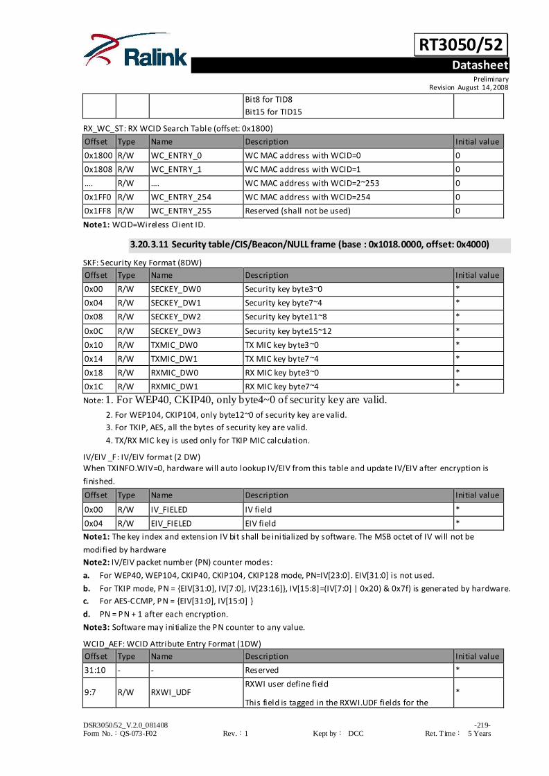
RT3050/52 Datasheet
Preliminary Revision August 14, 2008
DSR3050/52_V.2.0_081408 -219- Form No.:QS-073-F02 Rev.:1 Kept by: DCC Ret. T ime: 5 Years
Bit8 for TID8
Bit15 for TID15
RX_WC_ST: RX WCID Search Table (offset: 0x1800)
Offset Type Name Description Initial value
0x1800 R/W WC_ENTRY_0 WC MAC address with WCID=0 0
0x1808 R/W WC_ENTRY_1 WC MAC address with WCID=1 0
…. R/W …. WC MAC address with WCID=2~253 0
0x1FF0 R/W WC_ENTRY_254 WC MAC address with WCID=254 0
0x1FF8 R/W WC_ENTRY_255 Reserved (shall not be used) 0
Note1: WCID=Wireless Client ID.
3.20.3.11 Security table/CIS/Beacon/NULL frame (base : 0x1018.0000, offset: 0x4000)
SKF: Security Key Format (8DW)
Offset Type Name Description Initial value
0x00 R/W SECKEY_DW0 Security key byte3~0 *
0x04 R/W SECKEY_DW1 Security key byte7~4 *
0x08 R/W SECKEY_DW2 Security key byte11~8 *
0x0C R/W SECKEY_DW3 Security key byte15~12 *
0x10 R/W TXMIC_DW0 TX MIC key byte3~0 *
0x14 R/W TXMIC_DW1 TX MIC key byte7~4 *
0x18 R/W RXMIC_DW0 RX MIC key byte3~0 *
0x1C R/W RXMIC_DW1 RX MIC key byte7~4 *
Note: 1. For WEP40, CKIP40, only byte4~0 of security key are valid.
2. For WEP104, CKIP104, only byte12~0 of security key are valid.
3. For TKIP, AES, all the bytes of security key are valid.
4. TX/RX MIC key is used only for TKIP MIC calculation.
IV/EIV _F: IV/EIV format (2 DW) When TXINFO.WIV=0, hardware will auto lookup IV/EIV from this table and update IV/EIV after encryption is
finished.
Offset Type Name Description Initial value
0x00 R/W IV_FIELED IV field *
0x04 R/W EIV_FIELED EIV field *
Note1: The key index and extension IV bit shall be initialized by software. The MSB octet of IV will not be
modified by hardware
Note2: IV/EIV packet number (PN) counter modes:
a. For WEP40, WEP104, CKIP40, CKIP104, CKIP128 mode, PN=IV[23:0]. EIV[31:0] is not used.
b. For TKIP mode, PN = {EIV[31:0], IV[7 :0], IV[23:16]}, IV[15:8]=(IV[7:0] | 0x20) & 0x7f) is generated by hardware.
c. For AES-CCMP, PN = {EIV[31:0], IV[15:0] }
d. PN = PN + 1 after each encryption.
Note3: Software may initialize the PN counter to any value.
WCID_AEF: WCID Attribute Entry Format (1DW)
Offset Type Name Description Initial value
31:10 - - Reserved *
9:7 R/W RXWI_UDF RXWI user define field
This field is tagged in the RXWI.UDF fields for the *

RT3050/52 Datasheet
Preliminary Revision August 14, 2008
DSR3050/52_V.2.0_081408 -220- Form No.:QS-073-F02 Rev.:1 Kept by: DCC Ret. T ime: 5 Years
WCID.
6:4 R/W BSS_IDX Multiple-BSS index for the WCID *
3:1 R/W RX_PKEY_MODE
Pair-wise key security mode
0: No security
1: WEP40
2: WEP104
3: TKIP
4: AES-CCMP
5: CKIP40
6: CKIP104
7: CKIP128
*
0 R/W RX_PKEY_EN
Key table selection
0: shared key table
1: pair-wise key table
*
SKME: Share Key Mode Entry Format (1DW)
Bits Type Name Description Initial value
31 - - Reserved *
30:28 R/W SKEY_MODE_7+ Shared key7+(8x) mode, x=0~3 *
27 - - Reserved *
26:24 R/W SKEY_MODE_6+ Shared key6+(8x) mode, x=0~3 *
23 - - Reserved *
22:20 R/W SKEY_MODE_5+ Shared key5+(8x) mode, x=0~3 *
19 - - Reserved *
18:16 R/W SKEY_MODE_4+ Shared key4+(8x) mode, x=0~3 *
15 - - Reserved *
14:12 R/W SKEY_MODE_3+ Shared key3+(8x) mode, x=0~3 *
11 - - Reserved *
10:8 R/W SKEY_MODE_2+ Shared key2+(8x) mode, x=0~3 *
7 - - Reserved *
6:4 R/W SKEY_MODE_1+ Shared key1+(8x) mode, x=0~3 *
3 - - Reserved *
2:0 R/W SKEY_MODE_0+ Shared key0+(8x) mode, x=0~3 *
Key mode definition:
0: No security
1: WEP40
2: WEP104
3: TKIP
4: AES-CCMP
5: CKIP40
6: CKIP104
7: CKIP128

RT3050/52 Datasheet
Preliminary Revision August 14, 2008
DSR3050/52_V.2.0_081408 -221- Form No.:QS-073-F02 Rev.:1 Kept by: DCC Ret. T ime: 5 Years
3.20.3.12 Security Table
PWKT: Pair-Wise Key Table (offset: 0x4000)
Offset Type Name Description Initial value
0x4000 R/W PKEY_0 Pair-wise key for WCID0 *
0x4020 R/W PKEY_1 Pair-wise key for WCID1 *
…. R/W …. Pair-wise key for WCID2~253 *
0x5FC0 R/W PKEY_254 Pair-wise key for WCID254 *
0x5FE0 R/W PKEY_255 Pair-wise key for WCID255 (not used) *
IV/EIV _T: IV/EIV table (offset: 0x6000)
Offset Type Name Description Initial value
0x6000 R/W IVEIV_0 IV/EIV for WCID0 *
0x6008 R/W IVEIV_1 IV/EIV for WCID1 *
…. R/W …. IV/EIV for WCID2~253 *
0x67F0 R/W IVEIV_254 IV/EIV for WCID254 *
0x67F8 R/W IVEIV_255 IV/EIV for WCID255 (not used) *
WCID_AT: WCID Attribute Table (offset: 0x6800)
Offset Type Name Description Initial value
0x6800 R/W WCID_ATTR_0 WCID Attribute for WCID0 *
0x6804 R/W WCID_ATTR_1 WCID Attribute for WCID1 *
…. R/W …. WCID Attribute for WCID2~253 *
0x6BF8 R/W WCID_ATTR_254 WCID Attribute for WCID254 *
0x6BFC R/W WCID_ATTR_255 WCID Attribute for WCID255 *
SKT: Shared Key Table (offset: 0x6C00)
Offset Type Name Description Initial value
0x6C00 R/W SKEY_0 Shared key for BSS_IDX=0, KEY_IDX=0 *
0x6C20 R/W SKEY_1 Shared key for BSS_IDX=0, KEY_IDX=1 *
0x6C40 R/W SKEY_2 Shared key for BSS_IDX=0, KEY_IDX=2 *
0x6C60 R/W SKEY_3 Shared key for BSS_IDX=0, KEY_IDX=3 *
0x6C80 R/W SKEY_4 Shared key for BSS_IDX=1, KEY_IDX=0 *
0x6CA0 R/W SKEY_5 Shared key for BSS_IDX=1, KEY_IDX=1 *
0x6CC0 R/W SKEY_6 Shared key for BSS_IDX=1, KEY_IDX=2 *
0x6CE0 R/W SKEY_7 Shared key for BSS_IDX=1, KEY_IDX=3 *
0x6D00 R/W SKEY_8 Shared key for BSS_IDX=2, KEY_IDX=0 *
0x6D20 R/W SKEY_9 Shared key for BSS_IDX=2, KEY_IDX=1 *
0x6D40 R/W SKEY_10 Shared key for BSS_IDX=2, KEY_IDX=2 *
0x6D60 R/W SKEY_11 Shared key for BSS_IDX=2, KEY_IDX=3 *
0x6D80 R/W SKEY_12 Shared key for BSS_IDX=3, KEY_IDX=0 *
0x6DA0 R/W SKEY_13 Shared key for BSS_IDX=3, KEY_IDX=1 *
0x6DC0 R/W SKEY_14 Shared key for BSS_IDX=3, KEY_IDX=2 *
0x6DE0 R/W SKEY_15 Shared key for BSS_IDX=3, KEY_IDX=3 *
0x6E00 R/W SKEY_16 Shared key for BSS_IDX=4, KEY_IDX=0 *
0x6E20 R/W SKEY_17 Shared key for BSS_IDX=4, KEY_IDX=1 *

RT3050/52 Datasheet
Preliminary Revision August 14, 2008
DSR3050/52_V.2.0_081408 -222- Form No.:QS-073-F02 Rev.:1 Kept by: DCC Ret. T ime: 5 Years
0x6E40 R/W SKEY_18 Shared key for BSS_IDX=4, KEY_IDX=2 *
0x6E60 R/W SKEY_19 Shared key for BSS_IDX=4, KEY_IDX=3 *
0x6E80 R/W SKEY_20 Shared key for BSS_IDX=5, KEY_IDX=0 *
0x6EA0 R/W SKEY_21 Shared key for BSS_IDX=5, KEY_IDX=1 *
0x6EC0 R/W SKEY_22 Shared key for BSS_IDX=5, KEY_IDX=2 *
0x6EE0 R/W SKEY_23 Shared key for BSS_IDX=5, KEY_IDX=3 *
0x6F00 R/W SKEY_24 Shared key for BSS_IDX=6, KEY_IDX=0 *
0x6F20 R/W SKEY_25 Shared key for BSS_IDX=6, KEY_IDX=1 *
0x6F40 R/W SKEY_26 Shared key for BSS_IDX=6, KEY_IDX=2 *
0x6F60 R/W SKEY_27 Shared key for BSS_IDX=6, KEY_IDX=3 *
0x6F80 R/W SKEY_28 Shared key for BSS_IDX=7, KEY_IDX=0 *
0x6FA0 R/W SKEY_29 Shared key for BSS_IDX=7, KEY_IDX=1 *
0x6FC0 R/W SKEY_30 Shared key for BSS_IDX=7, KEY_IDX=2 *
0x6FE0 R/W SKEY_31 Shared key for BSS_IDX=7, KEY_IDX=3 *
SKM: Shared Key Mode (offset: 0x7000)
Offset Type Name Description Initial value
0x7000 R/W SKEY_MODE_0_7 Shared mode for SKEY0-SKEY7 *
0x7004 R/W SKEY_MODE_8_15 Shared mode for SKEY8-SKEY15 *
0x7008 R/W SKEY_MODE_16_23 Shared mode forSKEY16-SKEY23 *
0x700C R/W SKEY_MODE_24_31 Shared mode for SKEY24-SKEY31 *

RT3050/52 Datasheet
Preliminary Revision August 14, 2008
DSR3050/52_V.2.0_081408 -223- Form No.:QS-073-F02 Rev.:1 Kept by: DCC Ret. T ime: 5 Years
3.20.3.13 Descriptor and Wireless information
3.20.3.13.1 TX frame information
To transmit a frame, the driver needs to prepare the TX frame information for
hardware. The TX frame information contains the transmission control, the
header, and the payload. The transmission control information (the “TXWI”) is
used by the MAC and BBP and is applied for the associated TX frame when
transmission. The header and payload is the content of an 802.11 packet.
The TX information could be scattered in several segments. The TX descriptor (the
“TXD”) specifies the location and length of the TX frame information segment. TX
frame information could be linked by use of several TXD. These TXD are arranged in
a TXD ring in serial. Below diagram illustrates the linking between TXD and TX frame
information.
TXD(0)
SDP0 SDL0, LS0 = 0
TXD(0)
SDP1 SDL1, LS1 = 0
TXWI(4DW)
802.11 header
TX payload
(segment 0)
TX payload
(segment 1)
TX payload
(segment n)
TXD(1)
SDP0 SDL0, LS0 = 0
TXD(1)
SDP1 SDL1, LS1 = 0
TXD(k)
SDP0 SDL0, LS0 = 0
TXD(k)
SDP1 SDL1, LS1 = 1
TXD(0).SDP0
TXD(0).SDP1
TXD(1).SDP0
TXD(k).SDP1
TXD ring
TXD for
TX frame i
Fig. 3-20-3 TX frame Information

RT3050/52 Datasheet
Preliminary Revision August 14, 2008
DSR3050/52_V.2.0_081408 -224- Form No.:QS-073-F02 Rev.:1 Kept by: DCC Ret. T ime: 5 Years
3.20.3.13.2 TX descriptor format
SDP0[31:0]
SDL0[13:0]
D
D
O
N
E
L
S
0SDL1[13:0]
B
u
r
s
t
L
S
1
SDP1[31:0]
QSEL
W
I
VRSV[23:0]RSV[4:0]
bit 31 bit 0
Fig. 3-20-4 TX Descriptor Format
SDP0 : Segment Data Pointer 0
SDL0 : Segment Data Length for the data pointed by SDP0.
SDP1 : Segment Data Pointer 1.
SDL1 : Segment Data Length for the data pointed by SDP1.
LS0 : data pointed by SDP0 is the last segment
LS1 : data pointed by SDP1 is the last segment
DDONE : DMA Done. DMA has transferred the segments pointed by this TX descriptor
3.20.3.13.3 TXWI format
MPDU total byte count[11:0]
T
S
A
M
P
D
U
C
F
A
C
K
MCS[6:0]
MPDU
desity
[2:0]
M
I
M
O
O
F
D
M
M
M
P
S
TX Packet
ID[3:0]
F
R
A
G
IV [31:0]
EIV [31:0]
WCID[7:0] BAWinSize[5:0]
N
S
E
Q
A
C
K
B
W
S
G
I
STB
C
Reserved
[2:0]Reserved[5:0]
TXO
P
[1:0]
bit 31 bit 0
Fig. 3-20-5 TXWI Format
FRAG: 1: to inform TKIP engine this is a fragment, so that TKIP MIC is appended by driver at the
last fragment; hardware TKIP engine only need to insert IV/EIV and ICV
RT3050/52 Datasheet
Preliminary Revision August 14, 2008
DSR3050/52_V.2.0_081408 -225- Form No.:QS-073-F02 Rev.:1 Kept by: DCC Ret. T ime: 5 Years
MMPS: 1: the remote peer is in dynamic MIMO-PS mode
CFACK: 1: if an ACK is required to the same peer as this outgoing DATA frame, then MAC TX will
send a single DATA+CFACK frame instead of separate ACK and DATA frames. 0: no piggyback ACK
allowed for the RA of this frame.
TS: 1: This is a BEACON or ProbeResponse frame and MAC needs to auto insert 8 -byte timestamp
after 802.11 WLAN header.
AMPDU: this frame is eligible for AMPDU. MAC TX will aggregate subsequent outgoing frames
having <same RA, same TID, AMPDU=1> whenever TXOP allows. Even there’s only one DATA
frame to be sent, as long as the AMPDU bit in TXWI is ON, MAC will still package it as AMPDU with
implicit BAR. This adds only 4-byte AMPDU delimiter overhead into the outgoing frame and imply
the response frame is a BA instead of ACK. NOTE: driver should set AMPDU=1 only after a BA
session is successfully negotiated, because Block ACK is the only way to acknowledge in AMPDU
case.
MPDU density: 1/4usec ~ 16usec per-peer parameter used in outgoing A-MPDU. (This field
complies with the “minimum MDPU Starting Spacing” of the A-MPDU parameter field of draft
1.08).
000- no restriction
001- 1/4 μsec
010- 1/2 μsec
011- 1 μsec
100- 2 μse
101- 4 μsec
110- 8 μsec
111- 16 μsec
TXOP: TX back off mode. 0: HT TXOP rule; 1: PIFS TX ; 2: SIFS (only when previous frame exchange
is successful); 3: Back off.
“MCS/BW/ShortGI/OFDM/MIMO”: TX data rate & MIMO parameters for this outgoing frame to
be fi lled into BBP.
ACK: this bit informs MAC to wait for ACK or not after transmission of the frame. Event though
QOD DATA frame has ACK policy in its QOS CONTROL field, MAC TX solely depends on this ACK bit
to decide waiting of ACK or not.
NSEQ: 1: to use the special h/w SEQ number register in MAC block.
BA window size: tell MAC the maximum number of to-be-BAed frames is allowed of the RA (RA’s
BA re-ordering buffer size)
WCID (Wireless Client Index) : lookup result of ADDR1 in the peer table (255=not found). This
index is also used to find all the attributes of the wireless peer (e.g. TX rate, TX power, pair-wise
KEY, IV, EIV,). This index has consistent meaning in both driver and hardware.
MSDU total byte count: total length of this frame.
Packet ID: as a cookie specified by driver and will be latched into the TX result register stack.
Driver use this field to identify special frame’s TX result.
IV: used by encryption engine.
EIV: used by encryption engine.

RT3050/52 Datasheet
Preliminary Revision August 14, 2008
DSR3050/52_V.2.0_081408 -226- Form No.:QS-073-F02 Rev.:1 Kept by: DCC Ret. T ime: 5 Years
3.20.3.13.4 RX descriptor ring
The RX descriptor (the “RXD”) specifies the location to place the payload of the received frame
(the RX payload) and the associated receiving information (the “RXWI”). One RXD serves for
one receiving frame. Only SDP0 and SDL0 are useful in the RXD. The RXD is arranged in the RXD
ring in serial. The hardware links the RXWI and RX payload in serial and place it to the l ocation
specified in SDP0. See below diagram.
RXD(0)
SDP0 SDL0, LS0
RXD(0)
SDP1 SDL1, LS1
RXWI(4DW)
RX payloadRXD(1)
SDP0 SDL0, LS0
RXD(1)
SDP1 SDL1, LS1
RXD(0).SDP0
RXD ring
RXD for
RX frame i
RXD for
RX frame i+1
RXWI(4DW)
RX payload
RXD(1).SDP0
RXD(2)
SDP0 SDL0, LS0
RXD(2)
SDP1 SDL1, LS1
RXD for
RX frame i+2
Fig. 3-20-6 RX Descriptor Ring
3.20.3.13.5 RX descriptor format
SDP0[31:0]
D
D
O
N
E
L
S
0SDL1[13:0]0 1
SDP1[31:0]
A
M
P
D
U
15'b0
bit 31 bit 0
L
2
p
a
d
R
S
S
I
H
T
C
A
M
S
D
U
M
I
C
E
R
R
I
C
V
E
R
R
C
R
C
E
R
R
M
Y
B
S
S
B
C
M
C
U
C
2
M
E
F
R
A
G
N
U
L
L
D
A
T
A
B
A
SDL0[13:0]
D
E
C
Fig. 3-20-7 RX Descriptor Format

RT3050/52 Datasheet
Preliminary Revision August 14, 2008
DSR3050/52_V.2.0_081408 -227- Form No.:QS-073-F02 Rev.:1 Kept by: DCC Ret. T ime: 5 Years
Following fields are driver-specified.
SDP0 : Segment Data Pointer 0.
SDL0 : Segment Data Length for the data pointed by SDP0.
SDP1 : Segment Data Pointer 1.
SDL1 : Segment Data Length for the data pointed by SDP1.
DDONE : DMA Done. DMA has moved the RX frame to the speci fied location.
Set by hardware and cleared by driver.
Following fields are filled by hardware.
BA: the received frame is part of BA session, need to do re-ordering.
DATA : 1: the received frame is DATA type.
NULL: 1: the received frame has sub-type NULL/QOS-NULL.
FRAG: 1: the receive frame is a fragment
UC2ME: 1: the received frame ADDR1 = my MAC address
MC: 1: the received frame ADDR1 = multicast
BC: 1: the received frame ADDR1 = ff:ff:ff:ff:ff:ff
MyBSS: 1 : the received frame BSSID is one of my BSS (as an AP, max 4 BSSID supported)
CRC error: 1: the rec eived frame is CRC error
ICV error: 1: the rec eived frame is ICV error
MIC error: 1: the received frame is MIC error (RX CNRL register should support individual pass -up
error frame to driver in order to implement MIC error detection feature)
AMSDU: the received frame is in A-MSDU sub frame format which is <802.3 + MSDU + padding>
HTC : 1: this received frame came with HTC field, 0: no HTC field
RSSI: 1: RSSI information available in RSSI0, RSSI1, RSSI2 fields
L2Pad: 1: the L2 header is recognizable and been 2-byte-padded to ensure payload to align at 4-byte
boundary. 0: L2 header not extra padded
AMPDU: 1: this is an AMPDU segregated frame
DEC: 1 : this is a decrypted frame
3.20.3.13.6 RXWI format
TID
[3:0]WCID[7:0]
UDF
[2:0]
MPDU total byte
count[11:0]
BSS
idx
[2:0]
Key
idx
[1:0]
bit 31 bit 0
RSV[15:0] SNR_0[7:0]SNR_1[7:0]
FN[3:0]STBC
[1:0]
S
G
I
B
W SN[11:0]MCS[6:0]PHY
mode
[1:0]
RSV
[2:0]
RSV[7:0] RSSI_0[7:0]RSSI_1[7:0]RSSI_2[7:0]
Fig. 3-20-8 RXWI Format

RT3050/52 Datasheet
Preliminary Revision August 14, 2008
DSR3050/52_V.2.0_081408 -228- Form No.:QS-073-F02 Rev.:1 Kept by: DCC Ret. T ime: 5 Years
WCID: index of ADDR2 in the pair wise KEY table. This value uniquely identifies the TA. WCID=255
means not found.
KEY Index : 0~3 extracted from IV field. For driver reference only, no particular usage so far.
BSSID index: 0~7 for BSSID0~7. Extract from 802.11 header (the last three bits of BSSID field)
UDF : User Defined Field.
MPDU total byte count: the entire MPDU length.
TID: extracted from 8002.11 QOS control field.
FN: fragment number of the received MPDU. Extract from 802.11 header.
SN: sequenc e number of the received MPDU. Used for BA re-ordering especially that AMSDU are auto
segregated by hardware and lost the 802.11 header.
“MCS/BW/SGI/PHYmode”: RX data rate & related MIMO parameters of this frame got from PLCP
header. See next section for the detail.
RSSI0 , RSSI1, RSSI2: BBP reported RSSI information of the received frame.
SNR0, SNR1: BBP reported SNR information of the received frame.
3.20.3.13.7 Brief PHY rate format and definition
A 16-bit brief PHY rate is used in MAC hardware.
It is the same PHY rate field described in TXWI and RXWI.
Bit Name Description
15:14 PHY MODE Preamble mode
0: Legacy CCK, 1: Legacy OFDM, 2: HT mix mode, 3 : HT green field
13:11 - Reserved
10:9 - Reserved
8 SGI Short Guard Interval, only support for HT mode 0: 800ns, 1: 400ns
7 BW Bandwidth Support both legacy and HT modes 40Mhz in legacy mode means duplicate legacy
0: 20Mhz, 1: 40Mhz
6:0 MCS Modulation Coding Scheme
Table. Brief PHY rate format
MODE = Legacy CCK
MCS = 0 Long Preamble CCK 1Mbps
MCS = 1 Long Preamble CCK 2Mbps
MCS = 2 Long Preamble CCK 5.5Mbps
MCS = 3 Long Preamble CCK 11Mbps
MCS = 8 Short Preamble CCK 1Mbps
* i llegal rate
MCS = 9 Short Preamble CCK 2Mbps
MCS = 10 Short Preamble 5.5Mbps
MCS = 11 Short Preamble 11Mbps
Other MCS codes are reserved in legacy CCK mode.
BW and SGI are reserved in legacy CCK mode.
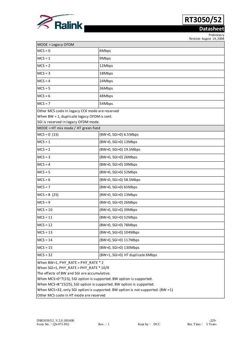
RT3050/52 Datasheet
Preliminary Revision August 14, 2008
DSR3050/52_V.2.0_081408 -229- Form No.:QS-073-F02 Rev.:1 Kept by: DCC Ret. T ime: 5 Years
MODE = Legacy OFDM
MCS = 0 6Mbps
MCS = 1 9Mbps
MCS = 2 12Mbps
MCS = 3 18Mbps
MCS = 4 24Mbps
MCS = 5 36Mbps
MCS = 6 48Mbps
MCS = 7 54Mbps
Other MCS code in legacy CCK mode are reserved
When BW = 1, duplicate legacy OFDM is sent.
SGI is reserved in legacy OFDM mode.
MODE = HT mix mode / HT green field
MCS = 0 (1S) (BW=0, SGI=0) 6.5Mbps
MCS = 1 (BW=0, SGI=0) 13Mbps
MCS = 2 (BW=0, SGI=0) 19.5Mbps
MCS = 3 (BW=0, SGI=0) 26Mbps
MCS = 4 (BW=0, SGI=0) 39Mbps
MCS = 5 (BW=0, SGI=0) 52Mbps
MCS = 6 (BW=0, SGI=0) 58.5Mbps
MCS = 7 (BW=0, SGI=0) 65Mbps
MCS = 8 (2S) (BW=0, SGI=0) 13Mbps
MCS = 9 (BW=0, SGI=0) 26Mbps
MCS = 10 (BW=0, SGI=0) 39Mbps
MCS = 11 (BW=0, SGI=0) 52Mbps
MCS = 12 (BW=0, SGI=0) 78Mbps
MCS = 13 (BW=0, SGI=0) 104Mbps
MCS = 14 (BW=0, SGI=0) 117Mbps
MCS = 15 (BW=0, SGI=0) 130Mbps
MCS = 32 (BW=1, SGI=0) HT duplicate 6Mbps
When BW=1, PHY_RATE = PHY_RATE * 2
When SGI=1, PHY_RATE = PHY_RATE * 10/9
The effects of BW and SGI are accumulative.
When MCS=0~7(1S), SGI option is supported. BW option is supported.
When MCS=8~15(2S), SGI option is supported. BW option is supported.
When MCS=32, only SGI option is supported. BW option is not supported. (BW =1)
Other MCS code in HT mode are reserved

RT3050/52 Datasheet
Preliminary Revision August 14, 2008
DSR3050/52_V.2.0_081408 -230- Form No.:QS-073-F02 Rev.:1 Kept by: DCC Ret. T ime: 5 Years
3.20.3.14 Driver implementation note
3.20.3.14.1 nstruction of down load 8051 firmware
1. Select on-chip program memory
i. SYS_CTRL.HST_PM_SEL (0x0400.bit[16]) =1
2. Write firmware into program memory space, which starts at 0x2000.
3. Close on-chip program memory.
i . SYS_CTRL.HST_PM_SEL (0x0400.bit[16]) =0
4. 8051 starts
3.20.3.14.2 Instruction of initialize DMA
1. Set base addresses and total number of descriptors:
i . TX_BASE_PTR0~TX_BASE_PTR5
ii. RX_BASE_PTR
iii . TX_MAX_CNT0~TX_MAX_CNT
iv. RX_MAX_CNT
2. Set WMM parameters
i. WMM_AIFSN_CFG
ii. WMM_CWMIN_CFG
iii . WMM_CWMAX_CFG
iv. WMM_TXOP0_CFG and WMM_TXOP1_CFG
3. Set DMA global configuration except TX_DMA_EN and RX_DMA_EN bits:
i . WPDMA_GLO_CFG
4. Set interrupt configuration:
i . DELAY_INT_CFG
5. Enable DMA interrupt:
i . INT_MASK
6. Enable DMA:
i. WPDMA_GLO_CFG.TX_DMA_EN = 1
WPDMA_GLO_CFG.RX_DMA_EN = 1
3.20.3.14.3 Instruction of clock control
3.20.3.14.3.1 Clock turn-off sequence
1. Switch 80MHz main clock to PLL clock:
i . Set SYS_CTRL.CLKSELECT = 1
2. Turn clock off:
i . Set SYS_CTRL.MAC_CLK_EN = 0
ii .Set SYS_CTRL.DMA_CLK_EN = 0
3. Turn off PLL:
i . Set PWR_PIN_CFG.IO_PLL_PD = 1.
3.20.3.14.3.2 Clock turn-on sequence
1. Turn on PLL:
i . Set PWR_PIN_CFG.IO_PLL_PD = 0
2. Waiting at least $bbp_pll_ready for PLL clock stable:
3. Turn on clock:
i . Set SYS_CTRL.MAC_CLK_EN = 1
ii . Set SYS_CTRL.DMA_CLK_EN = 1

RT3050/52 Datasheet
Preliminary Revision August 14, 2008
DSR3050/52_V.2.0_081408 -231- Form No.:QS-073-F02 Rev.:1 Kept by: DCC Ret. T ime: 5 Years
3.20.3.14.4 Instruction of TX/RX control
3.20.3.14.4.1 Freeze TX and RX sequence
1. Disable DMA TX:
i. Set WPDMA_GLO_CFG..TX_DMA_EN = 0
2. Polling until DMA TX becomes idle and PBF TX queue becomes empty:
i . Polling WPDMA_GLO_CFG. TX_DMA_BUSY = 0
ii . Polling TXRXQ_STA.TX0Q_STA = 2, TXRXQ_STA.TX1Q_STA = 2, polling
TXRXQ_STA.TX2Q_STA = 2.
iii . If the polling period > $dma_tx_polling_timeout, abort power saving procedure.
3. Disable MAC TX and RX:
i. Set MAC_SYS_CTRL.MAC_RX_EN = 0
ii . MAC_SYS_CTRL.MAC_TX_EN = 0
4. Polling until MAC TX and RX is disabled:
i . Polling MAC_STATUS_REG. TX_STATUS = 0, MAC_STATUS_REG. RX_STATUS = 0
ii . If the polling period > $mac_polling_timeout, abort power saving procedure.
5. Disable DMA RX:
i. Set WPDMA_GLO_CFG..RX_DMA_EN = 0 .
6. Polling until both DMA RX becomes idle and PBF RX queue becomes empty:
i . Polling WPDMA_GLO_CFG. RX_DMA_BUSY =0.
ii . Polling TXRXQ_STA.RX0Q_STA = 0x22.
iii . If the polling period > $dma_rx_polling_timeout, abort power saving procedure.
3.20.3.14.4.2 Recover TX and RX sequence
1. Enable DMA TX and RX:
i. Set WPDMA_GLO_CFG..RX_DMA_EN = 1
ii . Set WPDMA_GLO_CFG..TX_DMA_EN = 1
2. Enable MAC TX and RX:
i. Set MAC_SYS_CTRL.MAC_RX_EN = 1
ii . Set MAC_SYS_CTRL.MAC_TX_EN = 1
3.20.3.14.5 Instruction of RF power on/off sequence
1. Power down RF components sequence
i. Power down RF component
2. Set PWR_PIN_CFG.IO_ADDA_PD = 1.
3. Set PWR_PIN_CFG.IO_RF_PE = 0.
4. Set TX_PIN_CFG.TRSW_EN = 0.
5. Set TX_PIN_CFG.RFTR_EN = 0 .
6. Set TX_PIN_CFG.LNA_PE*EN = 0.
7. Set TX_PIN_CFG.PA_PE*EN = 0.
8. Enable RF components sequence
i. Recover the registers in previous sequence.
ii . Wait $rf_pll_ready for RF PLL becomes stable.
3.20.3.14.6 Power saving procedure
1. Freeze TX and RX
2. Power down LED and RF components
3. Clock turn-off
RT3050/52 Datasheet
Preliminary Revision August 14, 2008
DSR3050/52_V.2.0_081408 -232- Form No.:QS-073-F02 Rev.:1 Kept by: DCC Ret. T ime: 5 Years
3.20.3.14.7 Power recovery procedure
1. Clock turn-on
2. Enable LED and RF components
3. Recover TX and RX
3.20.3.14.8 Parameters
1. $rf_pll_ready = TBD.
2. $bbp_pll_ready = 500 us.
3. $dma_rx_polling_timeout = TBD.
4. $dma_tx_polling_timeout = TBD.
5. $mac_polling_timeout = TBD.

RT3050/52 Datasheet
Preliminary Revision August 14, 2008
DSR3050/52_V.2.0_081408 -233- Form No.:QS-073-F02 Rev.:1 Kept by: DCC Ret. T ime: 5 Years
4. Package Physical Dimension
4.1 TFBGA 289B(14×14×0.94mm)
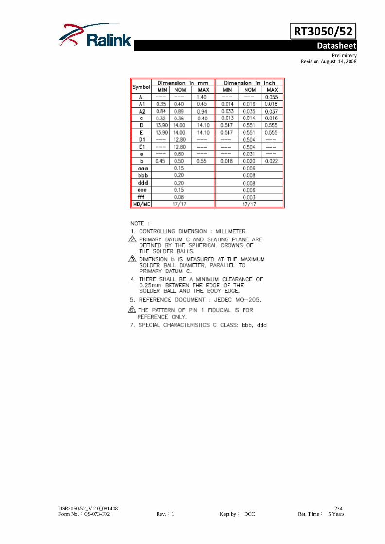
RT3050/52 Datasheet
Preliminary Revision August 14, 2008
DSR3050/52_V.2.0_081408 -234- Form No.:QS-073-F02 Rev.:1 Kept by: DCC Ret. T ime: 5 Years

RT3050/52 Datasheet
Preliminary Revision August 14, 2008
DSR3050/52_V.2.0_081408 -235- Form No.:QS-073-F02 Rev.:1 Kept by: DCC Ret. T ime: 5 Years
5. Revision History
Rev Date From Description
2.0 2008/8/14 Frank Lu Initial Release
This product is not designed for use in medical, life support applications. Do not use this product in these types of equipments or
applications .This document is subject to change without notice and Ralink assumes no responsibility for any inaccuracies that nay be contained
in this document. Ralink reserves the right to make change in the products to improve function, performance, reliability, and to attempt to
supply the best product possible.


