Embed Size (px)
Citation preview
v2.2
RTSX-S RadTolerant FPGAs
Designed for Space• SEU-Hardened Registers Eliminate the Need to
Implement Triple-Module Redundancy (TMR)– Immune to Single-Event Upsets (SEU) to LETth
> 40 MeV-cm2/mg, – SEU Rate < 10–10 Upset/Bit-Day in Worst-Case
Geosynchronous Orbit• Up to 100 krad (Si) Total Ionizing Dose (TID)
– Parametric Performance Supported with Lot-Specific Test Data
• Single-Event Latch-Up (SEL) Immunity• TM1019.5 Test Data Available• QML Certified Devices
High Performance• 230 MHz System Performance• 310 MHz Internal Performance• 9.5 ns Input Clock to Output Pad
Specifications• 0.25 µm Metal-to-Metal Antifuse Process• 48,000 to 108,000 Available System Gates• Up to 2,012 SEU-Hardened Flip-Flops• Up to 360 User-Programmable I/O Pins
Features• Very Low Power Consumption (Up to 68 mW at
Standby)• 3.3V and 5V Mixed Voltage• Configurable I/O Support for 3.3V/5V PCI, LVTTL,
TTL, and CMOS– 5V Input Tolerance and 5V Drive Strength– Slow Slew Rate Option– Configurable Weak Resistor Pull-Up/Down for
Tristated Outputs at Power-Up– Hot-Swap Compliant with Cold-Sparing
Support• Secure Programming Technology Prevents Reverse
Engineering and Design Theft• 100% Circuit Resource Utilization with 100% Pin
Locking• Unique In-System Diagnostic and Verification
Capability with Silicon Explorer II• Low-Cost Prototyping Option• Deterministic, User-Controllable Timing• JTAG Boundary Scan Testing in Compliance with
IEEE Standard 1149.1 – Dedicated JTAG Reset(TRST) Pin
™
eu
Table 1 • RTSX-S Product Profile
Device RT54SX32S RT54SX72S
CapacityTypical Gates System Gates
32,00048,000
72,000108,000
Logic ModulesCombinatorial CellsSEU-Hardened Register Cells (Dedicated Flip-Flops)
2,8801,8001,080
6,0364,0242,012
Maximum Flip-Flops 1,980 4,024
Maximum User I/Os 227 360
Clocks 3 3
Quadrant Clocks 0 4
Speed Grades Std., –1 Std., –1
Package (by pin count)CQFPCCGACCLG
208, 256
256
208, 256624
November 2004 i© 2004 Actel Corporation See Actel’s website for the latest version of the datasheet
RTSX-S RadTolerant FPGAs
Ordering Information
Temperature Grade and Application Offering
Ceramic Device ResourcesUser I/Os (including clock buffers)
Device CQFP
208-PinCQFP
256-PinCCLG
256-PinCCGA
624-Pin
RT54SX32S 173 227 202 –
RT54SX72S 170 212 – 360
Note: The 256-Pin CCLG available in Mil-Temp only.
Package RT54SX32S RT54SX72S
CQ208 B, E B, E
CQ256 B, E B, E
CC256 M –
CG624 – B, E
Note: M = Military TemperatureB = MIL-STD-883 Class B E = E-Flow
RT54SX72S CQ
Part Number
Package TypeCQ = Ceramic Quad Flat PackCG = Ceramic Column Grid Aray
256 B
Package Lead Count
Application (Temperature Range)B = MIL-STD-883 Class BE = E-Flow (Actel Space Level Flow)M = Military Temperature
Speed Grade
RT54SX32S =
Standard Speed Blank =1 Approximately 15% Faster than Standard=
1
72,000 RadTolerant Typical Gates32,000 RadTolerant Typical Gates
RT54SX72S =
CC = Ceramic Chip Carrier Land Grid
ii v2.2
RTSX-S RadTolerant FPGAs
Speed Grade and Temperature/Application Matrix
QML CertificationActel has achieved full QML certification, demonstrating that quality management procedures, processes, and controlsare in place and comply with MIL-PRF-38535 (the performance specification used by the U.S. Department of Defensefor monolithic integrated circuits).
Actel MIL-STD-883 Class B Product Flow
Std. –1
M
B
E
Step Screen 883 Method883 Class B
Requirement
1. Internal Visual 2010, Test Condition B 100%
2. Temperature Cycling 1010, Test Condition C 100%
3. Constant Acceleration 2001, Test Condition B or D,Y1, Orientation Only
100%
4. Particle Impact Noise Detection 2020, Condition A 100%
5. Seala. Fineb. Gross
1014100%100%
6. Visual Inspection 2009 100%
7. Pre-Burn-InElectrical Parameters
In accordance with applicable Actel device specification
100%
8. Dynamic Burn-In 1015, Condition D,160 hours at 125°C or 80 hours at 150°C
100%
9. Interim (Post-Burn-In)Electrical Parameters
In accordance with applicable Actel device specification
100%
10. Percent Defective Allowable 5% All Lots
11. Final Electrical Test
a. Static Tests(1)25°C(Subgroup 1, Table I)(2)–55°C and +125°C(Subgroups 2, 3, Table I)
b. Functional Tests(1)25°C(Subgroup 7, Table I)(2)–55°C and +125°C(Subgroups 8A and 8B, Table I)
c. Switching Tests at 25°C(Subgroup 9, Table I)
In accordance with applicable Actel device specification, which includes a, b, and c:
5005
5005
5005
5005
5005
100%
100%
100%
12. External Visual 2009 100%
v2.2 iii
RTSX-S RadTolerant FPGAs
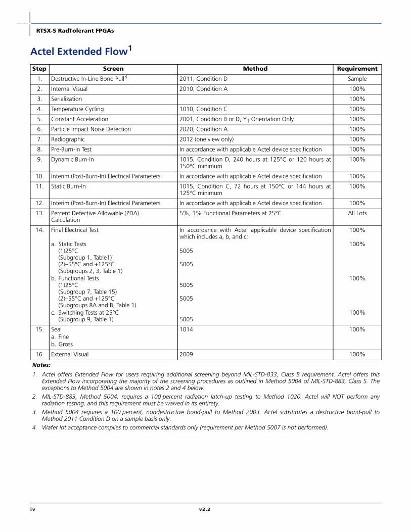
Actel Extended Flow1
Step Screen Method Requirement
1. Destructive In-Line Bond Pull3 2011, Condition D Sample
2. Internal Visual 2010, Condition A 100%
3. Serialization 100%
4. Temperature Cycling 1010, Condition C 100%
5. Constant Acceleration 2001, Condition B or D, Y1 Orientation Only 100%
6. Particle Impact Noise Detection 2020, Condition A 100%
7. Radiographic 2012 (one view only) 100%
8. Pre-Burn-In Test In accordance with applicable Actel device specification 100%
9. Dynamic Burn-In 1015, Condition D, 240 hours at 125°C or 120 hours at150°C minimum
100%
10. Interim (Post-Burn-In) Electrical Parameters In accordance with applicable Actel device specification 100%
11. Static Burn-In 1015, Condition C, 72 hours at 150°C or 144 hours at125°C minimum
100%
12. Interim (Post-Burn-In) Electrical Parameters In accordance with applicable Actel device specification 100%
13. Percent Defective Allowable (PDA) Calculation
5%, 3% Functional Parameters at 25°C All Lots
14. Final Electrical Test
a. Static Tests(1)25°C(Subgroup 1, Table1)(2)–55°C and +125°C(Subgroups 2, 3, Table 1)
b. Functional Tests(1)25°C(Subgroup 7, Table 15)(2)–55°C and +125°C(Subgroups 8A and B, Table 1)
c. Switching Tests at 25°C(Subgroup 9, Table 1)
In accordance with Actel applicable device specificationwhich includes a, b, and c:
5005
5005
5005
5005
5005
100%
100%
100%
100%
15. Seala. Fineb. Gross
1014 100%
16. External Visual 2009 100%
Notes:
1. Actel offers Extended Flow for users requiring additional screening beyond MIL-STD-833, Class B requirement. Actel offers thisExtended Flow incorporating the majority of the screening procedures as outlined in Method 5004 of MIL-STD-883, Class S. Theexceptions to Method 5004 are shown in notes 2 and 4 below.
2. MIL-STD-883, Method 5004, requires a 100 percent radiation latch-up testing to Method 1020. Actel will NOT perform anyradiation testing, and this requirement must be waived in its entirety.
3. Method 5004 requires a 100 percent, nondestructive bond-pull to Method 2003. Actel substitutes a destructive bond-pull toMethod 2011 Condition D on a sample basis only.
4. Wafer lot acceptance complies to commercial standards only (requirement per Method 5007 is not performed).
iv v2.2
Table of Contents
RTSX-S RadTolerant FPGAs
General DescriptionDevice Architecture . . . . . . . . . . . . . . . . . . . . . . . . . . . . . . . . . . . . . . . . . . . . . . . . . . 1-1
Programmable Interconnect Element . . . . . . . . . . . . . . . . . . . . . . . . . . . . . . . . . . . . 1-1
I/O Structure . . . . . . . . . . . . . . . . . . . . . . . . . . . . . . . . . . . . . . . . . . . . . . . . . . . . . . . . 1-2
Logic Modules . . . . . . . . . . . . . . . . . . . . . . . . . . . . . . . . . . . . . . . . . . . . . . . . . . . . . . . 1-2
Routing . . . . . . . . . . . . . . . . . . . . . . . . . . . . . . . . . . . . . . . . . . . . . . . . . . . . . . . . . . . . 1-2
Global Resources . . . . . . . . . . . . . . . . . . . . . . . . . . . . . . . . . . . . . . . . . . . . . . . . . . . . . 1-3
Design Environment . . . . . . . . . . . . . . . . . . . . . . . . . . . . . . . . . . . . . . . . . . . . . . . . . . 1-3
Programming . . . . . . . . . . . . . . . . . . . . . . . . . . . . . . . . . . . . . . . . . . . . . . . . . . . . . . . 1-5
Low-Cost Prototyping Solution . . . . . . . . . . . . . . . . . . . . . . . . . . . . . . . . . . . . . . . . . 1-5
In-System Diagnostic and Debug Capabilities . . . . . . . . . . . . . . . . . . . . . . . . . . . . . 1-5
Radiation Survivability . . . . . . . . . . . . . . . . . . . . . . . . . . . . . . . . . . . . . . . . . . . . . . . . 1-5
Summary . . . . . . . . . . . . . . . . . . . . . . . . . . . . . . . . . . . . . . . . . . . . . . . . . . . . . . . . . . . 1-6
Related Documents . . . . . . . . . . . . . . . . . . . . . . . . . . . . . . . . . . . . . . . . . . . . . . . . . . 1-6
Detailed SpecificationGeneral Conditions . . . . . . . . . . . . . . . . . . . . . . . . . . . . . . . . . . . . . . . . . . . . . . . . . . 2-1
Operating Conditions . . . . . . . . . . . . . . . . . . . . . . . . . . . . . . . . . . . . . . . . . . . . . . . . . 2-2
Thermal Characteristics . . . . . . . . . . . . . . . . . . . . . . . . . . . . . . . . . . . . . . . . . . . . . . . 2-4
Timing Model . . . . . . . . . . . . . . . . . . . . . . . . . . . . . . . . . . . . . . . . . . . . . . . . . . . . . . . 2-6
I/O Specifications . . . . . . . . . . . . . . . . . . . . . . . . . . . . . . . . . . . . . . . . . . . . . . . . . . . . 2-7
Module Specifications . . . . . . . . . . . . . . . . . . . . . . . . . . . . . . . . . . . . . . . . . . . . . . . 2-20
Routing Specifications . . . . . . . . . . . . . . . . . . . . . . . . . . . . . . . . . . . . . . . . . . . . . . . 2-25
Global Resources . . . . . . . . . . . . . . . . . . . . . . . . . . . . . . . . . . . . . . . . . . . . . . . . . . . . 2-27
Other Architectural Features . . . . . . . . . . . . . . . . . . . . . . . . . . . . . . . . . . . . . . . . . . 2-33
Package Pin Assignments208-Pin CQFP . . . . . . . . . . . . . . . . . . . . . . . . . . . . . . . . . . . . . . . . . . . . . . . . . . . . . . . . 3-1
256-Pin CQFP . . . . . . . . . . . . . . . . . . . . . . . . . . . . . . . . . . . . . . . . . . . . . . . . . . . . . . . . 3-5
256-Pin CCLG . . . . . . . . . . . . . . . . . . . . . . . . . . . . . . . . . . . . . . . . . . . . . . . . . . . . . . . 3-10
624-Pin CCGA . . . . . . . . . . . . . . . . . . . . . . . . . . . . . . . . . . . . . . . . . . . . . . . . . . . . . . 3-19
Datasheet InformationList of Changes . . . . . . . . . . . . . . . . . . . . . . . . . . . . . . . . . . . . . . . . . . . . . . . . . . . . . . 4-1
Datasheet Categories . . . . . . . . . . . . . . . . . . . . . . . . . . . . . . . . . . . . . . . . . . . . . . . . . 4-5
v2.2 v

RTSX-S RadTolerant FPGAs
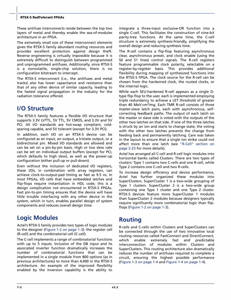
General Description
RTSX-S RadTolerant FPGAs are enhanced versions ofActel’s SX-A family of devices, specifically designed forenhanced radiation performance.
Featuring SEU-hardened D-type flip-flops that offer thebenefits of Triple Module Redundancy (TMR) without theassociated overhead, the RTSX-S family is a uniqueproduct offering for space applications. Manufacturedusing 0.25 µm technology at the Matsushita (MEC)facility in Japan, RTSX-S offers levels of radiationsurvivability far in excess of typical CMOS devices.
Device ArchitectureActel's RTSX-S architecture, derived from the highlysuccessful SX-A sea-of-modules architecture, has beendesigned to improve upset and total-dose performancein radiation environments.
With three layers of metal interconnect in the RT54SX32Sand four metal layers in RT54SX72S, the RTSX-S familyprovides efficient use of silicon by locating the routinginterconnect resources between the top two metallayers. This completely eliminates the channels of routingand interconnect resources between logic modules as
found in traditional FPGAs. In a sea-of-modulesarchitecture, the entire floor of the FPGA is covered witha grid of logic modules with virtually no chip area lost tointerconnect elements or routing.
The RTSX-S architecture adds several enhancements overthe SX-A architecture to improve its performance inradiation environments, such as SEU-hardened flip-flops,wider clock lines, and stronger clock drivers.
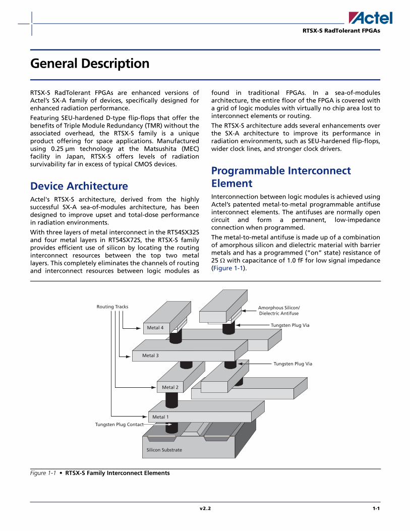
Programmable Interconnect ElementInterconnection between logic modules is achieved usingActel’s patented metal-to-metal programmable antifuseinterconnect elements. The antifuses are normally opencircuit and form a permanent, low-impedanceconnection when programmed.
The metal-to-metal antifuse is made up of a combinationof amorphous silicon and dielectric material with barriermetals and has a programmed (“on” state) resistance of25 Ω with capacitance of 1.0 fF for low signal impedance(Figure 1-1).
Figure 1-1 • RTSX-S Family Interconnect Elements
Silicon Substrate
Metal 4
Metal 3
Metal 2
Metal 1
Amorphous Silicon/ Dielectric Antifuse
Tungsten Plug Via
Tungsten Plug Via
Tungsten Plug Contact
Routing Tracks
v2.2 1-1
RTSX-S RadTolerant FPGAs
These antifuse interconnects reside between the top twolayers of metal and thereby enable the sea-of-modulesarchitecture in an FPGA.
The extremely small size of these interconnect elementsgives the RTSX-S family abundant routing resources andprovides excellent protection against design theft.Reverse engineering is virtually impossible because it isextremely difficult to distinguish between programmedand unprogrammed antifuses. Additionally, since RTSX-Sis a nonvolatile, single-chip solution, there is noconfiguration bitstream to intercept.
The RTSX-S interconnect (i.e., the antifuses and metaltracks) also has lower capacitance and resistance thanthat of any other device of similar capacity, leading tothe fastest signal propagation in the industry for theradiation tolerance offered.
I/O StructureThe RTSX-S family features a flexible I/O structure thatsupports 3.3V LVTTL, 5V TTL, 5V CMOS, and 3.3V and 5VPCI. All I/O standards are hot-swap compliant, cold-sparing capable, and 5V tolerant (except for 3.3V PCI).
In addition, each I/O on an RTSX-S device can beconfigured as an input, an output, a tristate output, or abidirectional pin. Mixed I/O standards are allowed andcan be set on a pin-by-pin basis. High or low slew ratecan be set on individual output buffers (except for PCI,which defaults to high slew), as well as the power-upconfiguration (either pull-up or pull-down).
Even without the inclusion of dedicated I/O registers,these I/Os, in combination with array registers, canachieve clock-to-output-pad timing as fast as 9.5 ns. Inmost FPGAs, I/O cells that have embedded latches andflip-flops require instantiation in HDL code; this is adesign complication not encountered in RTSX-S FPGAs.Fast pin-to-pin timing ensures that the device will havelittle trouble interfacing with any other device in thesystem, which in turn, enables parallel design of systemcomponents and reduces overall design time.
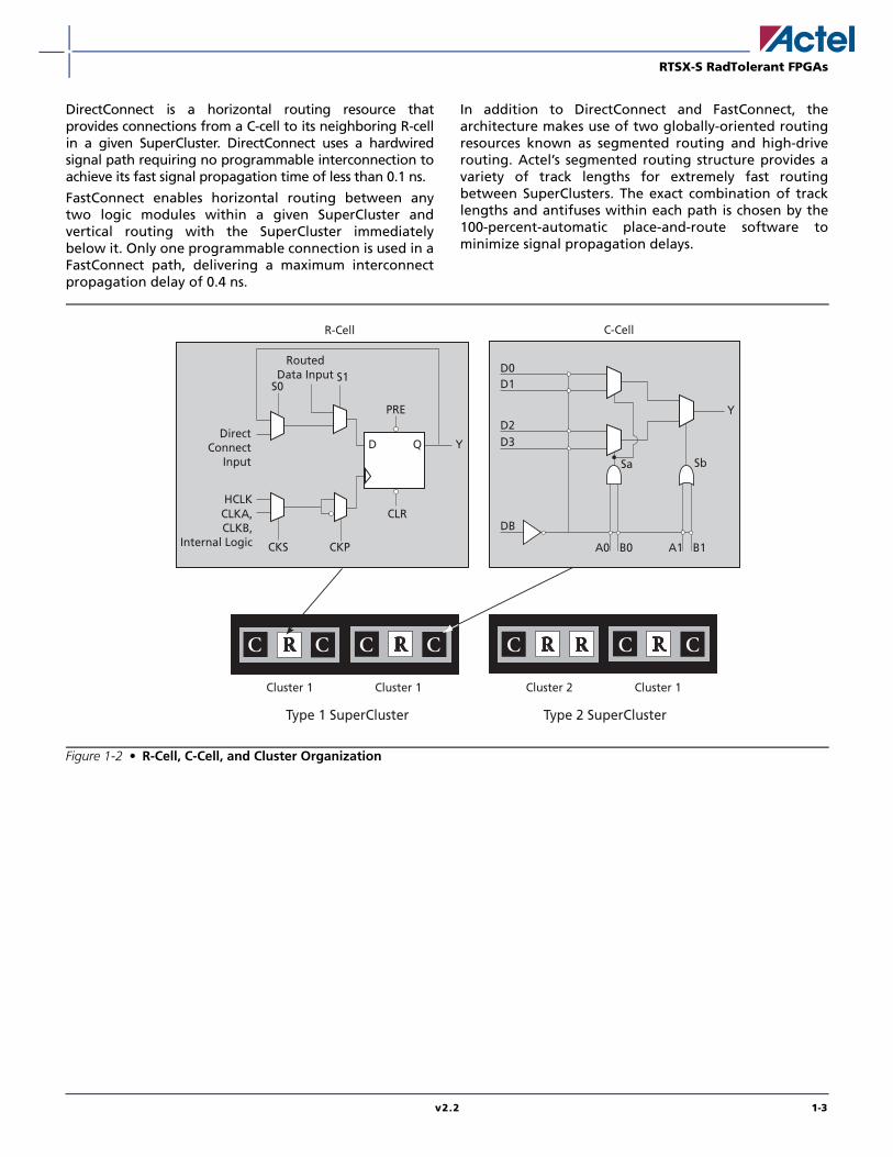
Logic ModulesActel’s RTSX-S family provides two types of logic modulesto the designer (Figure 1-2 on page 1-3): the register cell(R-cell) and the combinatorial cell (C-cell).
The C-cell implements a range of combinatorial functionswith up to 5 inputs. Inclusion of the DB input and itsassociated inverter function dramatically increases thenumber of combinatorial functions that can beimplemented in a single module from 800 options (as inprevious architectures) to more than 4,000 in the RTSX-Sarchitecture. An example of the improved flexibilityenabled by the inversion capability is the ability to
integrate a three-input exclusive-OR function into asingle C-cell. This facilitates the construction of nine-bitparity-tree functions. At the same time, the C-cellstructure is extremely synthesis-friendly, simplifying theoverall design and reducing synthesis time.
The R-cell contains a flip-flop featuring asynchronousclear, asynchronous preset, and clock enable (using theS0 and S1 lines) control signals. The R-cell registersfeature programmable clock polarity, selectable on aregister-by-register basis. This provides additionalflexibility during mapping of synthesized functions intothe RTSX-S FPGA. The clock source for the R-cell can bechosen from the hardwired clock, the routed clocks, orthe internal logic.
While each SEU-hardened R-cell appears as a single D-type flip-flop to the user, each is implemented employingtriple redundancy to achieve a LET threshold of greaterthan 40 MeV-cm2/mg. Each TMR R-cell consists of threemaster-slave latch pairs, each with asynchronous, self-correcting feedback paths. The output of each latch onthe master or slave side is voted with the outputs of theother two latches on that side. If one of the three latchesis struck by an ion and starts to change state, the votingwith the other two latches prevents the change fromfeeding back and permanently latching. Care was takenin the layout to ensure that a single ion strike could notaffect more than one latch (see "R-Cell" section onpage 2-23 for more details).
Actel has arranged all C-cell and R-cell logic modules intohorizontal banks called Clusters. There are two types ofclusters: Type 1 contains two C-cells and one R-cell, whileType 2 contains one C-cell and two R-cells.
To increase design efficiency and device performance,Actel has further organized these modules intoSuperClusters. SuperCluster 1 is a two-wide grouping ofType 1 clusters. SuperCluster 2 is a two-wide groupcontaining one Type 1 cluster and one Type 2 cluster.RTSX-S devices feature more SuperCluster 1 modulesthan SuperCluster 2 modules because designers typicallyrequire significantly more combinatorial logic than flip-flops (Figure 1-2 on page 1-3).
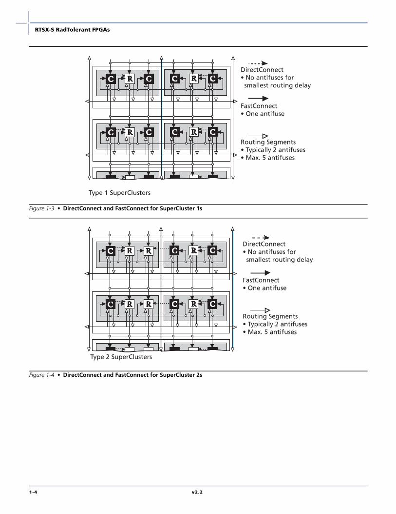
RoutingR-cells and C-cells within Clusters and SuperClusters canbe connected through the use of two innovative localrouting resources called FastConnect and DirectConnect,which enable extremely fast and predictableinterconnection of modules within Clusters andSuperClusters. This routing architecture also dramaticallyreduces the number of antifuses required to complete acircuit, ensuring the highest possible performance(Figure 1-3 on page 1-4 and Figure 1-4 on page 1-4).
1-2 v2.2
RTSX-S RadTolerant FPGAs
DirectConnect is a horizontal routing resource thatprovides connections from a C-cell to its neighboring R-cellin a given SuperCluster. DirectConnect uses a hardwiredsignal path requiring no programmable interconnection toachieve its fast signal propagation time of less than 0.1 ns.
FastConnect enables horizontal routing between anytwo logic modules within a given SuperCluster andvertical routing with the SuperCluster immediatelybelow it. Only one programmable connection is used in aFastConnect path, delivering a maximum interconnectpropagation delay of 0.4 ns.
In addition to DirectConnect and FastConnect, thearchitecture makes use of two globally-oriented routingresources known as segmented routing and high-driverouting. Actel’s segmented routing structure provides avariety of track lengths for extremely fast routingbetween SuperClusters. The exact combination of tracklengths and antifuses within each path is chosen by the100-percent-automatic place-and-route software tominimize signal propagation delays.
Figure 1-2 • R-Cell, C-Cell, and Cluster Organization
Type 1 SuperCluster Type 2 SuperCluster
Cluster 1 Cluster 1 Cluster 2 Cluster 1
R-Cell C-Cell
D0D1
D2D3
DB
A0 B0 A1 B1
Sa Sb
Y
DirectConnect
Input
CLKA,CLKB,
Internal Logic
HCLK
CKS CKP
CLR
PRE
YD Q
RoutedData Input
S0S1
v2.2 1-3
RTSX-S RadTolerant FPGAs
Figure 1-3 • DirectConnect and FastConnect for SuperCluster 1s
Figure 1-4 • DirectConnect and FastConnect for SuperCluster 2s
Type 1 SuperClusters
Routing Segments• Typically 2 antifuses• Max. 5 antifuses
FastConnect• One antifuse
DirectConnect• No antifuses for smallest routing delay
Type 2 SuperClusters
Routing Segments• Typically 2 antifuses• Max. 5 antifuses
FastConnect• One antifuse
DirectConnect• No antifuses for smallest routing delay
1-4 v2.2
RTSX-S RadTolerant FPGAs
Global ResourcesActel’s high-drive routing structure provides three clocknetworks: hardwired clocks (HCLK), routed clocks (CLKA,CLKB), and quadrant clocks (QCLKA, QCLKB, QCLKC,QCLKD).
The first clock, called HCLK, is hardwired from the HCLKbuffer to the clock select MUX in each R-cell. HCLKcannot be connected to combinational logic. Thisprovides a fast propagation path for the clock signal,enabling the 9.5 ns clock-to-out (pad-to-pad)performance of the RTSX-S devices.
The second type of clock, routed clocks, (CLKA, CLKB) areglobal clocks that can be sourced from either externalpins or internal logic signals within the device. CLKA andCLKB may be connected to sequential cells (R-cells) or tocombinational logic (C-cells).
The last type of clock, quadrant clocks, are only found inthe RT54SX72S. Similar to the routed clocks, the fourquadrant clocks (QCLKA, QCLKB, QCLKC, QCLKD) can besourced from external pins or from internal logic signalswithin the device. Each of these clocks can individuallydrive up to a quarter of the chip, or they can be groupedtogether to drive multiple quadrants.
Design Environment The RTSX-S family of FPGAs is fully supported by bothActel's Libero™ Integrated Design Environment (IDE)and Designer FPGA Development software. Actel LiberoIDE is a design management environment, seamlesslyintegrating design tools while guiding the user throughthe design flow, managing all design and log files, andpassing necessary design data among tools. Additionally,Libero IDE allows users to integrate both schematic andHDL synthesis into a single flow and verify the entiredesign in a single environment. Libero IDE includesSynplify® for Actel from Synplicity®, ViewDraw for Actelfrom Mentor Graphics, ModelSim™ HDL Simulator fromMentor Graphics®, WaveFormer Lite™ fromSynaptiCAD™, and Designer software from Actel. Referto the Libero IDE flow (located on Actel’s website)diagram for more information.
Actel's Designer software is a place-and-route tool andprovides a comprehensive suite of backend support toolsfor FPGA development. The Designer software includestiming-driven place-and-route, and a world-classintegrated static timing analyzer and constraints editor.With the Designer software, a user can select and lockpackage pins while only minimally impacting the resultsof place-and-route. Additionally, the back-annotationflow is compatible with all the major simulators and thesimulation results can be cross-probed with SiliconExplorer II, Actel’s integrated verification and logicanalysis tool. Another tool included in the Designersoftware is the ACTgen macro builder, which easilycreates popular and commonly used logic functions forimplementation into your schematic or HDL design.Actel's Designer software is compatible with the mostpopular FPGA design entry and verification tools fromcompanies such as Mentor Graphics, Synplicity, Synopsys,and Cadence Design Systems. The Designer software isavailable for both the Windows and UNIX operatingsystems.
ProgrammingProgramming support is provided through Actel's SiliconSculptor II, a single-site programmer driven via a PC-based GUI. Factory programming is available as well.
Low-Cost Prototyping SolutionSince the enhanced radiation characteristics of radiation-tolerant devices are not required during the prototypingphase of the design, Actel has developed a prototypingsolution for RTSX-S that utilizes commercial SX-A devices.The prototyping solution consists of two parts:
• A well-documented design flow that allows thecustomer to target an RTSX-S design to theequivalent commercial SX-A device
• Either footprint-compatible packages or protoypingsockets to adapt commercial SX-A packages to theRTAX-S package footprints
This methodology provides the user with a cost-effectivesolution while maintaining the short time-to-marketassociated with Actel FPGAs. Please see the applicationnote Prototyping for the RTSX-S Enhanced AerospaceFPGA for more details
Table 1-1 • RTSX-S Global Resources
RT54SX32S RT54SX72S
Routed Clocks (CLKA, CLKB) 2 2
Hardwired Clocks (HCLK) 1 1
Quadrant Clocks (QCLKA, QCLKB, QCLKC, QCLKD)
0 4
v2.2 1-5
RTSX-S RadTolerant FPGAs
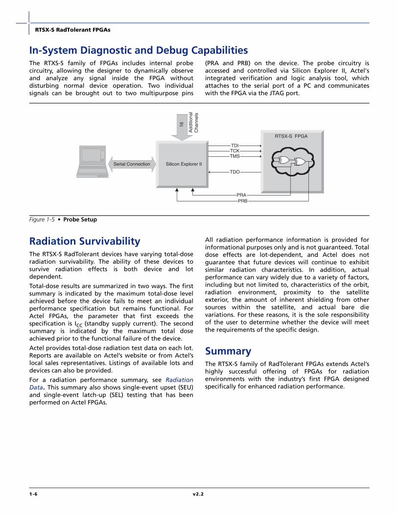
In-System Diagnostic and Debug CapabilitiesThe RTXS-S family of FPGAs includes internal probecircuitry, allowing the designer to dynamically observeand analyze any signal inside the FPGA withoutdisturbing normal device operation. Two individualsignals can be brought out to two multipurpose pins
(PRA and PRB) on the device. The probe circuitry isaccessed and controlled via Silicon Explorer II, Actel'sintegrated verification and logic analysis tool, whichattaches to the serial port of a PC and communicateswith the FPGA via the JTAG port.
Radiation SurvivabilityThe RTSX-S RadTolerant devices have varying total-doseradiation survivability. The ability of these devices tosurvive radiation effects is both device and lotdependent.
Total-dose results are summarized in two ways. The firstsummary is indicated by the maximum total-dose levelachieved before the device fails to meet an individualperformance specification but remains functional. ForActel FPGAs, the parameter that first exceeds thespecification is ICC (standby supply current). The secondsummary is indicated by the maximum total doseachieved prior to the functional failure of the device.
Actel provides total-dose radiation test data on each lot.Reports are available on Actel’s website or from Actel’slocal sales representatives. Listings of available lots anddevices can also be provided.
For a radiation performance summary, see RadiationData. This summary also shows single-event upset (SEU)and single-event latch-up (SEL) testing that has beenperformed on Actel FPGAs.
All radiation performance information is provided forinformational purposes only and is not guaranteed. Totaldose effects are lot-dependent, and Actel does notguarantee that future devices will continue to exhibitsimilar radiation characteristics. In addition, actualperformance can vary widely due to a variety of factors,including but not limited to, characteristics of the orbit,radiation environment, proximity to the satelliteexterior, the amount of inherent shielding from othersources within the satellite, and actual bare dievariations. For these reasons, it is the sole responsibilityof the user to determine whether the device will meetthe requirements of the specific design.
SummaryThe RTSX-S family of RadTolerant FPGAs extends Actel’shighly successful offering of FPGAs for radiationenvironments with the industry’s first FPGA designedspecifically for enhanced radiation performance.
Figure 1-5 • Probe Setup
Silicon Explorer II
TDITCK
TDO
TMS
PRAPRB
Serial Connection
16
Add
ition
al
Cha
nnel
s
RTSX-S FPGA
1-6 v2.2
RTSX-S RadTolerant FPGAs
Related Documents
Application NotesSimultaneous Switching Noise and Signal Integrity
http://www.actel.com/documents/SSN_AN.pdf
Implementation of Security in Actel Antifuse FPGAshttp://www.actel.com/documents/Antifuse_Security_AN.pdf
Using A54SX72A and RT54SX72S Quadrant Clocks
http://www.actel.com/documents/QCLK_AN.pdf
Actel eX, SX-A and RTSX-S I/Os
http://www.actel.com/documents/AntifuseIO_AN.pdf
IEEE Standard 1149.1 (JTAG) in the SX/RTSX/SX-A/eX/RT54SX-S Families
http://www.actel.com/documents/SX_SXAJTAG_AN.pdf
Prototyping for the RT54SX-S Enhanced Aerospace FPGA
http://www.actel.com/documents/RTSXS_Proto_AN.pdf
Actel CQFP to FBGA Adapter Socket Instructions
http://www.actel.com/documents/CQ352-FPGA_Adapter_AN.pdf
Actel SX-A and RT54SX-S Devices in Hot-Swap and Cold-Sparing Applications
http://www.actel.com/documents/HotSwapColdSparing_AN.pdf
User’s Guides and ManualsAntifuse Macro Library Guide
http://www.actel.com/documents/libguide.pdf
ACTgen Macros User’s Guide
http://www.actel.com/documents/genguide.pdf
Libero IDE v5.2 User's Guide
http://www.actel.com/documents/liberoUG.pdf
Silicon Sculptor II User’s Guidehttp://www.actel.com/techdocs/manuals/default.asp
White PapersDesign Security in Nonvolatile Flash and Antifuse FPGAshttp://www.actel.com/documents/DesignSecurity_WP.pdf
Understanding Actel Antifuse Device Security
http://www.actel.com/documents/AntifuseSecurityWP.pdf
v2.2 1-7

RTSX-S RadTolerant FPGAs
Detailed Specifications
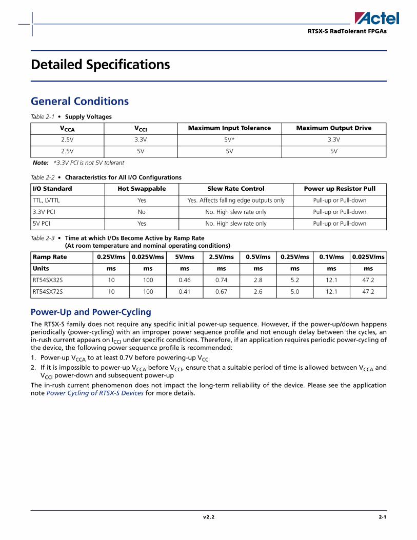
General Conditions
Power-Up and Power-CyclingThe RTSX-S family does not require any specific initial power-up sequence. However, if the power-up/down happensperiodically (power-cycling) with an improper power sequence profile and not enough delay between the cycles, anin-rush current appears on ICCI under specific conditions. Therefore, if an application requires periodic power-cycling ofthe device, the following power sequence profile is recommended:
1. Power-up VCCA to at least 0.7V before powering-up VCCI
2. If it is impossible to power-up VCCA before VCCI, ensure that a suitable period of time is allowed between VCCA andVCCI power-down and subsequent power-up
The in-rush current phenomenon does not impact the long-term reliability of the device. Please see the applicationnote Power Cycling of RTSX-S Devices for more details.
Table 2-1 • Supply Voltages
VCCA VCCI Maximum Input Tolerance Maximum Output Drive
2.5V 3.3V 5V* 3.3V
2.5V 5V 5V 5V
Note: *3.3V PCI is not 5V tolerant
Table 2-2 • Characteristics for All I/O Configurations
I/O Standard Hot Swappable Slew Rate Control Power up Resistor Pull
TTL, LVTTL Yes Yes. Affects falling edge outputs only Pull-up or Pull-down
3.3V PCI No No. High slew rate only Pull-up or Pull-down
5V PCI Yes No. High slew rate only Pull-up or Pull-down
Table 2-3 • Time at which I/Os Become Active by Ramp Rate(At room temperature and nominal operating conditions)
Ramp Rate 0.25V/ms 0.025V/ms 5V/ms 2.5V/ms 0.5V/ms 0.25V/ms 0.1V/ms 0.025V/ms
Units ms ms ms ms ms ms ms ms
RT54SX32S 10 100 0.46 0.74 2.8 5.2 12.1 47.2
RT54SX72S 10 100 0.41 0.67 2.6 5.0 12.1 47.2
v2.2 2-1
RTSX-S RadTolerant FPGAs
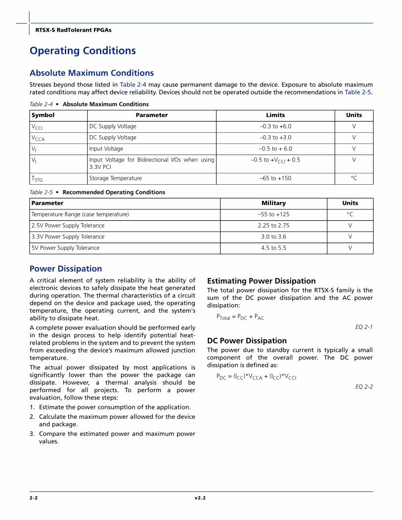
Operating Conditions
Absolute Maximum ConditionsStresses beyond those listed in Table 2-4 may cause permanent damage to the device. Exposure to absolute maximumrated conditions may affect device reliability. Devices should not be operated outside the recommendations in Table 2-5.
Power DissipationA critical element of system reliability is the ability ofelectronic devices to safely dissipate the heat generatedduring operation. The thermal characteristics of a circuitdepend on the device and package used, the operatingtemperature, the operating current, and the system'sability to dissipate heat.
A complete power evaluation should be performed earlyin the design process to help identify potential heat-related problems in the system and to prevent the systemfrom exceeding the device’s maximum allowed junctiontemperature.
The actual power dissipated by most applications issignificantly lower than the power the package candissipate. However, a thermal analysis should beperformed for all projects. To perform a powerevaluation, follow these steps:
1. Estimate the power consumption of the application.
2. Calculate the maximum power allowed for the deviceand package.
3. Compare the estimated power and maximum powervalues.
Estimating Power DissipationThe total power dissipation for the RTSX-S family is thesum of the DC power dissipation and the AC powerdissipation:
PTotal = PDC + PAC
EQ 2-1
DC Power DissipationThe power due to standby current is typically a smallcomponent of the overall power. The DC powerdissipation is defined as:
PDC = (ICC)*VCCA + (ICC)*VCCI
EQ 2-2
Table 2-4 • Absolute Maximum Conditions
Symbol Parameter Limits Units
VCCI DC Supply Voltage –0.3 to +6.0 V
VCCA DC Supply Voltage –0.3 to +3.0 V
VI Input Voltage –0.5 to + 6.0 V
VI Input Voltage for Bidirectional I/Os when using3.3V PCI
–0.5 to +VCCI + 0.5 V
TSTG Storage Temperature –65 to +150 °C
Table 2-5 • Recommended Operating Conditions
Parameter Military Units
Temperature Range (case temperature) –55 to +125 °C
2.5V Power Supply Tolerance 2.25 to 2.75 V
3.3V Power Supply Tolerance 3.0 to 3.6 V
5V Power Supply Tolerance 4.5 to 5.5 V
2-2 v2.2
RTSX-S RadTolerant FPGAs
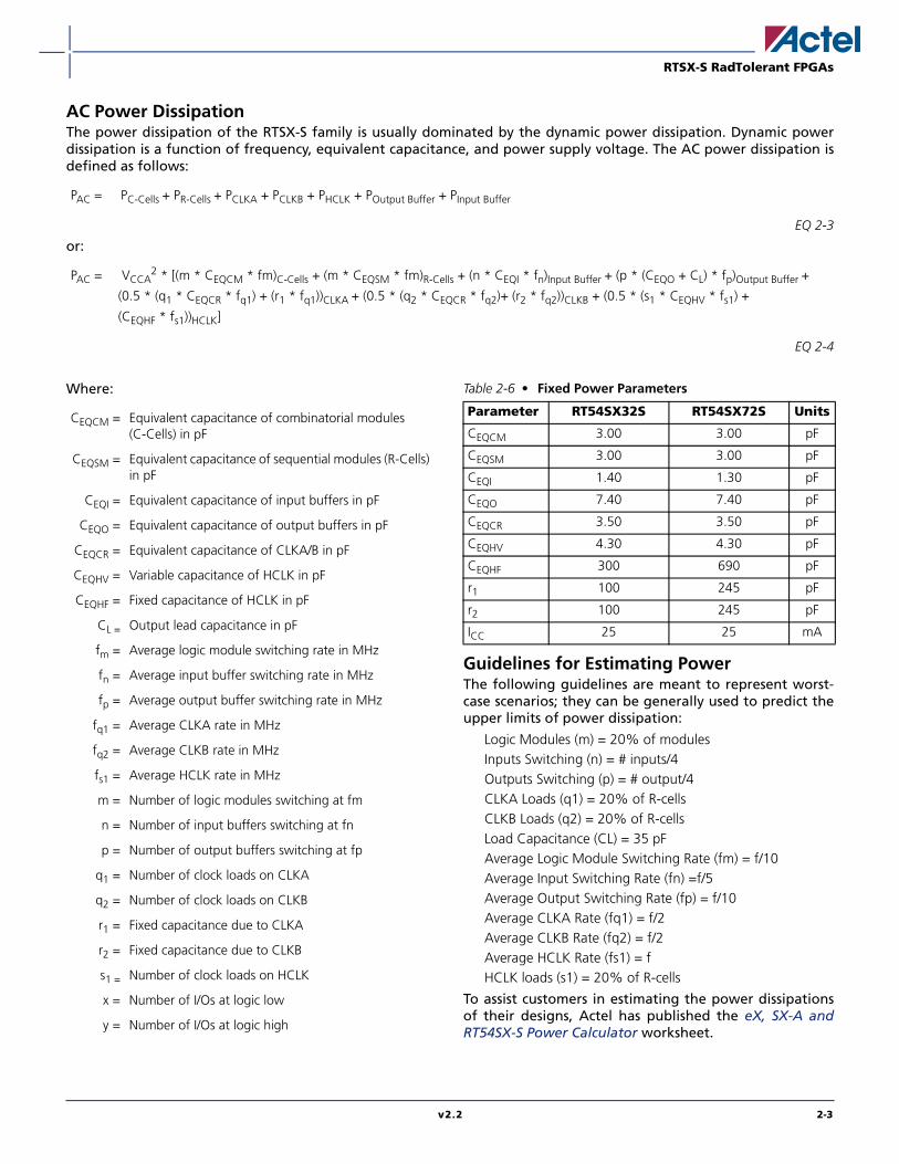
AC Power DissipationThe power dissipation of the RTSX-S family is usually dominated by the dynamic power dissipation. Dynamic powerdissipation is a function of frequency, equivalent capacitance, and power supply voltage. The AC power dissipation isdefined as follows:
EQ 2-3
or:
EQ 2-4
Where:
Guidelines for Estimating PowerThe following guidelines are meant to represent worst-case scenarios; they can be generally used to predict theupper limits of power dissipation:
Logic Modules (m) = 20% of modulesInputs Switching (n) = # inputs/4Outputs Switching (p) = # output/4CLKA Loads (q1) = 20% of R-cellsCLKB Loads (q2) = 20% of R-cellsLoad Capacitance (CL) = 35 pFAverage Logic Module Switching Rate (fm) = f/10Average Input Switching Rate (fn) =f/5Average Output Switching Rate (fp) = f/10Average CLKA Rate (fq1) = f/2Average CLKB Rate (fq2) = f/2Average HCLK Rate (fs1) = fHCLK loads (s1) = 20% of R-cells
To assist customers in estimating the power dissipationsof their designs, Actel has published the eX, SX-A andRT54SX-S Power Calculator worksheet.
PAC = PC-Cells + PR-Cells + PCLKA + PCLKB + PHCLK + POutput Buffer + PInput Buffer
PAC = VCCA2 * [(m * CEQCM * fm)C-Cells + (m * CEQSM * fm)R-Cells + (n * CEQI * fn)Input Buffer + (p * (CEQO + CL) * fp)Output Buffer +
(0.5 * (q1 * CEQCR * fq1) + (r1 * fq1))CLKA + (0.5 * (q2 * CEQCR * fq2)+ (r2 * fq2))CLKB + (0.5 * (s1 * CEQHV * fs1) +
(CEQHF * fs1))HCLK]
CEQCM = Equivalent capacitance of combinatorial modules (C-Cells) in pF
CEQSM = Equivalent capacitance of sequential modules (R-Cells) in pF
CEQI = Equivalent capacitance of input buffers in pF
CEQO = Equivalent capacitance of output buffers in pF
CEQCR = Equivalent capacitance of CLKA/B in pF
CEQHV = Variable capacitance of HCLK in pF
CEQHF = Fixed capacitance of HCLK in pF
CL = Output lead capacitance in pF
fm = Average logic module switching rate in MHz
fn = Average input buffer switching rate in MHz
fp = Average output buffer switching rate in MHz
fq1 = Average CLKA rate in MHz
fq2 = Average CLKB rate in MHz
fs1 = Average HCLK rate in MHz
m = Number of logic modules switching at fm
n = Number of input buffers switching at fn
p = Number of output buffers switching at fp
q1 = Number of clock loads on CLKA
q2 = Number of clock loads on CLKB
r1 = Fixed capacitance due to CLKA
r2 = Fixed capacitance due to CLKB
s1 = Number of clock loads on HCLK
x = Number of I/Os at logic low
y = Number of I/Os at logic high
Table 2-6 • Fixed Power Parameters
Parameter RT54SX32S RT54SX72S Units
CEQCM 3.00 3.00 pF
CEQSM 3.00 3.00 pF
CEQI 1.40 1.30 pF
CEQO 7.40 7.40 pF
CEQCR 3.50 3.50 pF
CEQHV 4.30 4.30 pF
CEQHF 300 690 pF
r1 100 245 pF
r2 100 245 pF
ICC 25 25 mA
v2.2 2-3
RTSX-S RadTolerant FPGAs
Thermal Characteristics
IntroductionThe temperature variable in Actel’s Designer softwarerefers to the junction temperature, not the ambient,case, or board temperatures. This is an importantdistinction because dynamic and static powerconsumption cause the chip junction to be higher thanthe ambient, case, or board temperatures. EQ 2-5, EQ 2-6, and EQ 2-7 give the relationship between thermalresistance, temperature gradient and power.
EQ 2-5
EQ 2-6
EQ 2-7
Where:
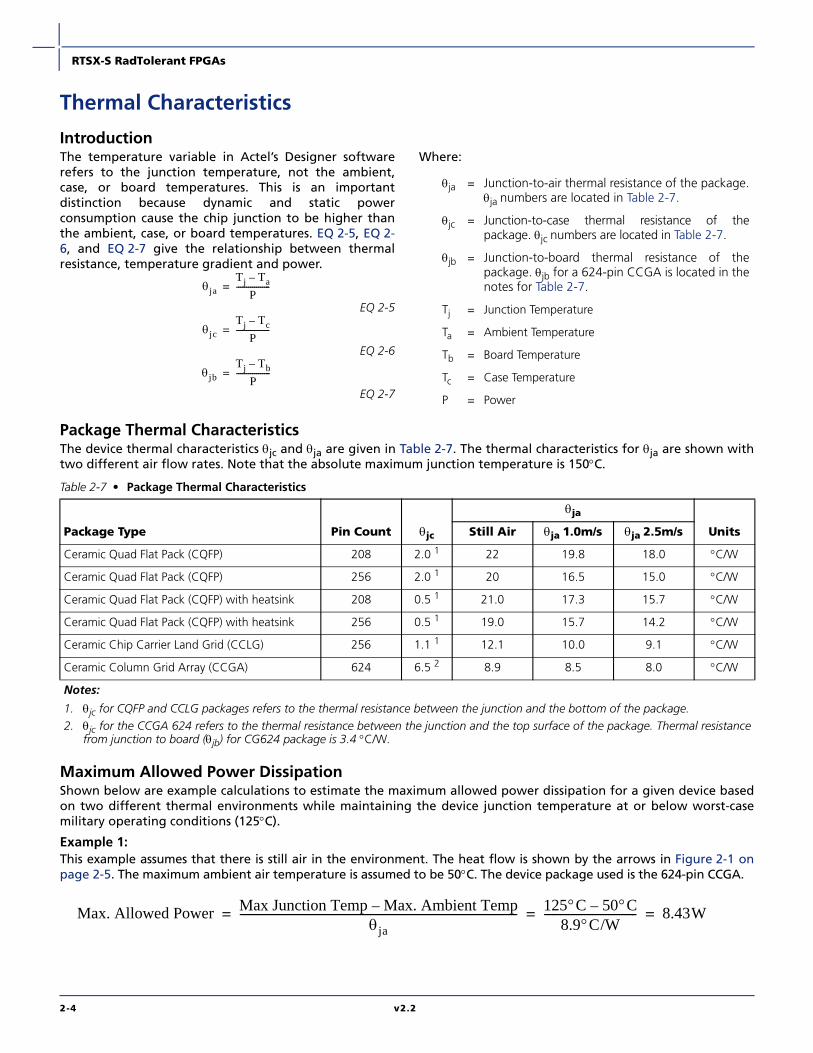
Package Thermal CharacteristicsThe device thermal characteristics θjc and θja are given in Table 2-7. The thermal characteristics for θja are shown withtwo different air flow rates. Note that the absolute maximum junction temperature is 150°C.
Maximum Allowed Power DissipationShown below are example calculations to estimate the maximum allowed power dissipation for a given device basedon two different thermal environments while maintaining the device junction temperature at or below worst-casemilitary operating conditions (125°C).
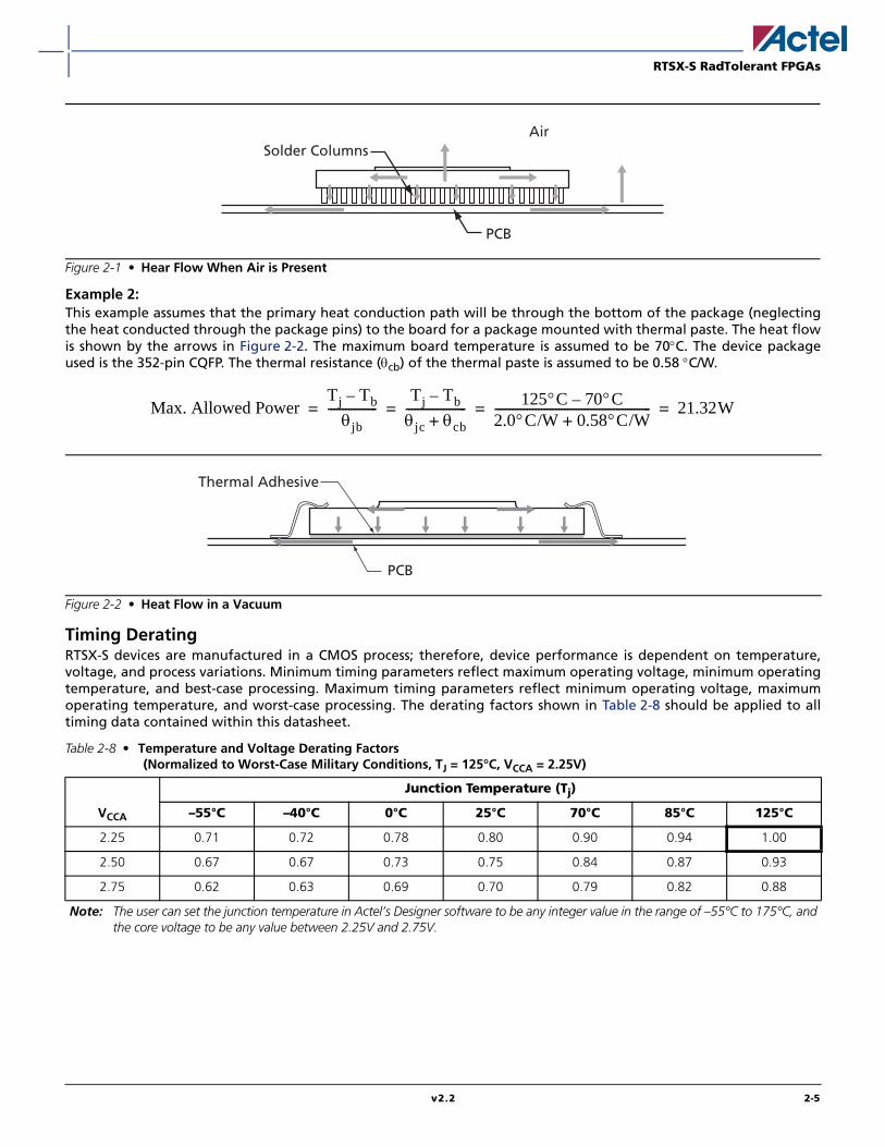
Example 1: This example assumes that there is still air in the environment. The heat flow is shown by the arrows in Figure 2-1 onpage 2-5. The maximum ambient air temperature is assumed to be 50°C. The device package used is the 624-pin CCGA.
θjaTj Ta–
P-----------------=
θjcTj Tc–
P-----------------=
θjbTj Tb–
P-----------------=
θja = Junction-to-air thermal resistance of the package.θja numbers are located in Table 2-7.
θjc = Junction-to-case thermal resistance of thepackage. θjc numbers are located in Table 2-7.
θjb = Junction-to-board thermal resistance of thepackage. θjb for a 624-pin CCGA is located in thenotes for Table 2-7.
Tj = Junction Temperature
Ta = Ambient Temperature
Tb = Board Temperature
Tc = Case Temperature
P = Power
Table 2-7 • Package Thermal Characteristics
Package Type Pin Count θjc
θja
UnitsStill Air θja 1.0m/s θja 2.5m/s
Ceramic Quad Flat Pack (CQFP) 208 2.0 1 22 19.8 18.0 °C/W
Ceramic Quad Flat Pack (CQFP) 256 2.0 1 20 16.5 15.0 °C/W
Ceramic Quad Flat Pack (CQFP) with heatsink 208 0.5 1 21.0 17.3 15.7 °C/W
Ceramic Quad Flat Pack (CQFP) with heatsink 256 0.5 1 19.0 15.7 14.2 °C/W
Ceramic Chip Carrier Land Grid (CCLG) 256 1.1 1 12.1 10.0 9.1 °C/W
Ceramic Column Grid Array (CCGA) 624 6.5 2 8.9 8.5 8.0 °C/W
Notes:
1. θjc for CQFP and CCLG packages refers to the thermal resistance between the junction and the bottom of the package.2. θjc for the CCGA 624 refers to the thermal resistance between the junction and the top surface of the package. Thermal resistance
from junction to board (θjb) for CG624 package is 3.4 °C/W.
Max. Allowed Power Max Junction Temp Max. Ambient Temp–θja
-------------------------------------------------------------------------------------------------------- 125°C 50°C–8.9°C/W
----------------------------------- 8.43W= = =
2-4 v2.2
RTSX-S RadTolerant FPGAs
Example 2: This example assumes that the primary heat conduction path will be through the bottom of the package (neglectingthe heat conducted through the package pins) to the board for a package mounted with thermal paste. The heat flowis shown by the arrows in Figure 2-2. The maximum board temperature is assumed to be 70°C. The device packageused is the 352-pin CQFP. The thermal resistance (θcb) of the thermal paste is assumed to be 0.58 °C/W.
Timing DeratingRTSX-S devices are manufactured in a CMOS process; therefore, device performance is dependent on temperature,voltage, and process variations. Minimum timing parameters reflect maximum operating voltage, minimum operatingtemperature, and best-case processing. Maximum timing parameters reflect minimum operating voltage, maximumoperating temperature, and worst-case processing. The derating factors shown in Table 2-8 should be applied to alltiming data contained within this datasheet.
Figure 2-1 • Hear Flow When Air is Present
Solder ColumnsAir
PCB
Figure 2-2 • Heat Flow in a Vacuum
Table 2-8 • Temperature and Voltage Derating Factors(Normalized to Worst-Case Military Conditions, TJ = 125°C, VCCA = 2.25V)
VCCA
Junction Temperature (Tj)
–55°C –40°C 0°C 25°C 70°C 85°C 125°C
2.25 0.71 0.72 0.78 0.80 0.90 0.94 1.00
2.50 0.67 0.67 0.73 0.75 0.84 0.87 0.93
2.75 0.62 0.63 0.69 0.70 0.79 0.82 0.88
Note: The user can set the junction temperature in Actel’s Designer software to be any integer value in the range of –55°C to 175°C, andthe core voltage to be any value between 2.25V and 2.75V.
Max. Allowed PowerTj Tb–
θjb-----------------
Tj Tb–
θjc θcb+--------------------- 125°C 70°C–
2.0°C/W 0.58°C/W+------------------------------------------------------ 21.32W= = = =
Thermal Adhesive
PCB
v2.2 2-5
RTSX-S RadTolerant FPGAs
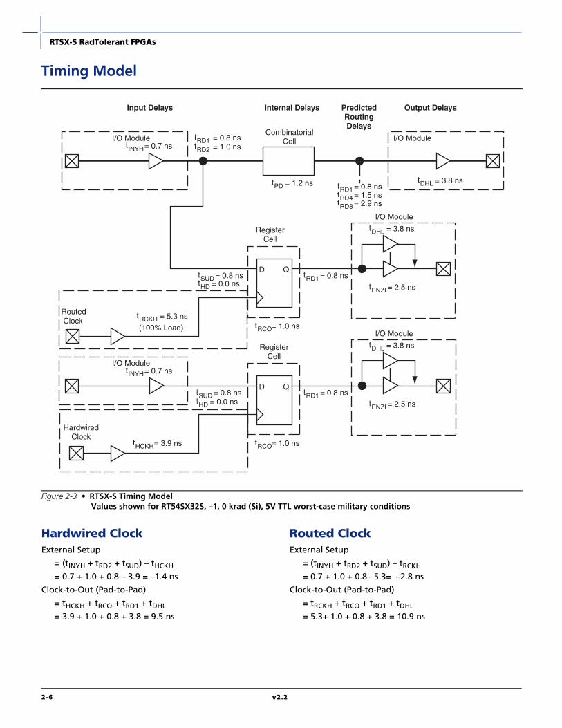
Timing Model
Hardwired ClockExternal Setup
= (tINYH + tRD2 + tSUD) – tHCKH
= 0.7 + 1.0 + 0.8 – 3.9 = –1.4 ns
Clock-to-Out (Pad-to-Pad)
= tHCKH + tRCO + tRD1 + tDHL
= 3.9 + 1.0 + 0.8 + 3.8 = 9.5 ns
Routed ClockExternal Setup
= (tINYH + tRD2 + tSUD) – tRCKH
= 0.7 + 1.0 + 0.8– 5.3= –2.8 ns
Clock-to-Out (Pad-to-Pad)
= tRCKH + tRCO + tRD1 + tDHL
= 5.3+ 1.0 + 0.8 + 3.8 = 10.9 ns
Figure 2-3 • RTSX-S Timing ModelValues shown for RT54SX32S, –1, 0 krad (Si), 5V TTL worst-case military conditions
Input Delays Internal Delays PredictedRoutingDelays
Output Delays
I/O ModuletINYH= 0.7 ns tRD2 = 1.0 ns
tRD1 = 0.8 nsCombinatorial
Cell I/O Module
tDHL = 3.8 ns
tRD8 = 2.9 nstRD4 = 1.5 nstRD1 = 0.8 nstPD = 1.2 ns
I/O ModuletDHL = 3.8 ns
tRD1 = 0.8 ns
tRCO= 1.0 ns
I/O ModuletINYH= 0.7 ns
tENZL= 2.5 ns
tSUD = 0.8 nstHD = 0.0 ns
tSUD = 0.8 nstHD = 0.0 ns
tRCKH = 5.3 ns
(100% Load)
D Q
RegisterCell
Routed Clock
tRD1 = 0.8 ns
tRCO= 1.0 nstHCKH= 3.9 ns
D Q
RegisterCell
HardwiredClock
I/O ModuletDHL = 3.8 ns
tENZL= 2.5 ns
2-6 v2.2
RTSX-S RadTolerant FPGAs
I/O Specifications
Pin Descriptions
Supply PinsGND Ground
Low supply voltage.
VCCI Supply Voltage
Supply voltage for I/Os. See Table 2-1 on page 2-1.
VCCA Supply Voltage
Supply voltage for Array. See Table 2-1 on page 2-1.
Global PinsCLKA/B Routed Clock A and B
These pins are clock inputs for clock distributionnetworks. Input levels are compatible with standard TTL,LVTTL, 3.3V PCI, or 5V PCI specifications. The clock inputis buffered prior to clocking the R-cells. When not used,this pin must be set Low or High on the board. Whenused, this pin should be held Low or High during power-up to avoid unwanted static power.
For RT54SX72S, these pins can be configured as user I/Os.When used, this pin offers a built-in programmable pull-up or pull-down resistor active during power-up only.
QCLKA/B/C/D Quadrant Clock A, B, C, and D / I/O
These four pins are the quadrant clock inputs and areonly found on the RT54SX72S. They are clock inputs forclock distribution networks. Input levels are compatiblewith standard TTL, LVTTL, 3.3V PCI or 5V PCIspecifications. Each of these clock inputs can drive up toa quarter of the chip, or they can be grouped together todrive multiple quadrants. The clock input is bufferedprior to clocking the core cells.
These pins can be configured as user I/Os. When notused, these pins must not be left floating. They must beset Low or High on the board. When used, this pin offersa built-in programmable pull-up or pull-down resistor,active during power-up only.
HCLK Dedicated (Hardwired) Array Clock
This pin is the clock input for sequential modules. Inputlevels are compatible with standard TTL, LVTTL, 3.3V PCI or5V PCI specifications. This input is buffered prior toclocking the R-cells. It offers clock speeds independent ofthe number of R-cells being driven. When not used, thispin must not be left floating. It must be set to Low or Highon the board. When used, this pin should be held Low orHigh during power-up to avoid unwanted static power.
JTAG/Probe PinsPRA/PRB1 I/O, Probe A/B
The probe pin is used to output data from any user-defined design node within the device. This independentdiagnostic pin can be used in conjunction with the otherprobe pin to allow real-time diagnostic output of anysignal path within the device. The probe pin can be usedas a user-defined I/O when verification has beencompleted. The pin’s probe capabilities can bepermanently disabled to protect programmed designconfidentiality.
TCK1, I/O Test Clock
Test clock input for diagnostic probe and deviceprogramming. In flexible mode, TCK becomes activewhen the TMS pin is set Low (Table 2-32 on page 2-35).This pin functions as an I/O when the boundary scanstate machine reaches the “logic reset” state.
TDI1, I/O Test Data Input
Serial input for boundary scan testing and diagnosticprobe. In flexible mode, TDI is active when the TMS pin isset Low (Table 2-32 on page 2-35). This pin functions asan I/O when the boundary scan state machine reachesthe “logic reset” state.
TDO1, I/O Test Data Output
Serial output for boundary scan testing. In flexible mode,TDO is active when the TMS pin is set Low (Table 2-32 onpage 2-35). This pin functions as an I/O when theboundary scan state machine reaches the "logic reset"state. When Silicon Explorer II is being used, TDO will actas an output when the "checksum" command is run. Itwill return to user I/O when "checksum" is complete.
TMS1 Test Mode Select
The TMS pin controls the use of the IEEE 1149.1boundary scan pins (TCK, TDI, TDO, TRST). In flexiblemode when the TMS pin is set Low, the TCK, TDI, andTDO pins are boundary scan pins (Table 2-32 on page 2-35). Once the boundary scan pins are in test mode, theywill remain in that mode until the internal boundaryscan state machine reaches the “logic reset” state. At thispoint, the boundary scan pins will be released and willfunction as regular I/O pins. The “logic reset” state isreached five TCK cycles after the TMS pin is set High. Indedicated test mode, TMS functions as specified in theIEEE 1149.1 specifications.
1. These pins should be terminated with a 70 Ω resistor to preserve probing capabilities.
v2.2 2-7
RTSX-S RadTolerant FPGAs
TRST Boundary Scan Reset Pin
The TRST pin functions as an active-low input toasynchronously initialize or rest the boundary scancircuit. The TRST pin is equipped with an internal pull-upresistor. For flight applications, the TRST pin should behardwired to GND.
User I/OI/O Input/Output
The I/O pin functions as an input, output, tristate, orbidirectional buffer. Input and output levels arecompatible with standard TTL, LVTTL, 3.3V/5V PCI, or 5VCMOS specifications. Unused I/O pins are automaticallytristated by the Designer software. See "User I/O" sectionon page 2-8 for more details.
Special FunctionsNC No Connection
This pin is not connected to circuitry within the device.These pins can be driven to any voltage or can be leftfloating with no effect on the operation of the device.
User I/O The RTSX-S family features a flexible I/O structure thatsupports 3.3V LVTTL, 5V TTL, 5V CMOS, and 3.3V and 5VPCI. All I/O standards are hot-swap compliant, cold-sparing capable, and 5V tolerant (except for 3.3V PCI).
Each I/O module has an available power-up resistor ofapproximately 50 kΩ that can configure the I/O to aknown state during power-up. Just slightly before VCCAreaches 2.5V, the resistors are disabled so the I/Os willbehave normally. For more information about thepower-up resistors, please see Actel’s application noteSX-A and RTSX-S Devices in Hot-Swap and Cold SparingApplications.
RTSX-S inputs should be driven by high-speed push-pulldevices with a low-resistance pull-up device. If the inputvoltage is greater than VCCI and a fast push-pull device isNOT used, the high-resistance pull-up of the driver andthe internal circuitry of the RTSX-S I/O may create avoltage divider (when a user I/O is configured as aninput, the associated output buffer is tristated). Thisvoltage divider could pull the input voltage belowspecification for some devices connected to the driver. Alogic ‘1’ may not be correctly presented in this case. Forexample, if an open drain driver is used with a pull-upresistor to 5V to provide the logic ‘1’ input, and VCCI is setto 3.3V on the RTSX-S device, the input signal may bepulled down by the RTSX-S input.
Hot SwappingRTSX-S I/Os can be configured to be hot swappable incompliance with the Compact PCI Specification.However, a 3.3V PCI device is not hot swappable. Duringpower-up/down, all I/Os are tristated. VCCA and VCCI donot have to be stable during power-up/down. After theRTSX-S device is plugged into an electrically activesystem, the device will not degrade the reliability of orcause damage to the host system. The device’s outputpins are driven to a high impedance state until normalchip operating conditions are reached. Table 2-3 onpage 2-1 summarizes the VCCA voltage at which the I/Osbehave according to the user’s design for an RTSX-Sdevice at room temperature for various ramp-up rates.The data reported assumes a linear ramp-up profile to2.5V. Refer to Actel’s application note, SX-A and RTSX-SDevices in Hot-Swap and Cold-Sparing Applications formore information on hot swapping.
Customizing the I/OEach user I/O on an RTSX-S device can be configured asan input, an output, a tristate output, or a bidirectionalpin. Mixed I/O standards are allowed and can be set on apin-by-pin basis. High or low slew rates can be set onindividual output buffers (except for PCI which defaultsto high slew), as well as the power-up configuration(either pull-up or pull-down).
The user selects the desired I/O by setting the I/Oproperties in PinEditor, Actel’s graphical pin-placementand I/O properties editor. See PinEditor online help formore information.
Unused I/OsAll unused user I/Os are automatically tristated by Actel’sDesigner software. Although termination is notrequired, it is recommended that the user tie off allunused I/Os to GND externally. If the I/O clamp diode isdisabled, then unused I/Os are 5V tolerant, otherwiseunused I/Os are tolerant to VCCI.
2-8 v2.2
RTSX-S RadTolerant FPGAs
I/O MacrosThere are nine I/O macros available to the user for RTSX-S:
• CLKBUF/CLKBUFI: Clock Buffer, noninverting andinverting
• CLKBIBUF/CLKBIBUFI: Bidirectional Clock Buffer,noninverting and inverting
• QCLKBUF/QCLKBUFI: Quadrant Clock Buffer,noninverting and inverting
• QCLKBIBUF/QCLKBIBUFI: Quad Bidirectional ClockBuffer, noninverting and inverting
• HCLKBUF: Hardwired Clock Buffer
• INBUF: Input Buffer
• OUTBUF: Output Buffer
• TRIBUF: Tristate Buffer
• BIBUF: Bidirectional Buffer
Table 2-9 • User I/O Features
Function Description
Input Buffer Threshold Selections • 5V: CMOS, PCI, TTL
• 3.3V: PCI, LVTTL
Flexible Output Driver • 5V: CMOS, PCI, TTL
• 3.3V: PCI, LVTTL
• Selectable on an individual I/O basis
Output Buffer “Hot-Swap” Capability
• I/Os on an unpowered device does not sink the current (Power supplies are at 0V)
• Can be used for “cold sparing”
Individually selectable slew rate, high or low slew (The default is high slew rate). The slewrate selection only affects the falling edge of an output. There is no change on the risingedge of the output or any inputs.
Power-Up Individually selectable pull-ups and pull-downs during power-up (default is to power-upin tristate mode)
Enables deterministic power-up of a device
VCCA and VCCI can be powered in any order
v2.2 2-9
RTSX-S RadTolerant FPGAs
I/O Module Timing Characteristics
Figure 2-4 • Output Timing Model and Waveforms
Figure 2-5 • Input Timing Model and Waveforms
Figure 2-6 • AC Test Loads
To AC test loads (shown below)PADD
E
TRIBUFF
D
VCC
GND50%
PadVOL
VOH
tDLH
50%
tDHL
EVCC
GND50%
PadVOL
tENZL
50%
10%
tENLZ
EVCC
GND50%
VPad
GND
VOH
tENZH
50%
90%
tENHZ
VCC
VMEASVMEAS
VMEAS VMEAS
PAD YINBUF
Pad 0V
YGND
VCC
50% 50%
tINYH tINYL
VMEASVMEAS
VCCI
Load 1(Used to measure
Load 2(Used to measure enable delays)
35 pF
To the output
VCC GND
35 pF
To the output
R to VCC for tPZLR to GND for tPZHR = 1 kΩ
propagation delay)
under test
under test
Load 3(Used to measure disable delays)
5 pF
To the output
R to VCC for tPLZR to GND for tPHZR = 1 kΩ
under test
VCC GND
2-10 v2.2
RTSX-S RadTolerant FPGAs
5V TTL and 3.3V LVTTL Table 2-10 • 5V TTL and 3.3V LVTTL Electrical Specifications
Symbol
Military
Parameter Min. Max. Units
VOH VCCI = Min,VI = VIH or VIL
(IOH = -1mA) 0.9 VCCI V
VCCI = Min,VI = VIH or VIL
(IOH = -8mA) 2.4 V
VOL VCCI = Min,VI = VIH or VIL
(IOL= 1mA) 0.1 VCCI V
VCCI = Min,VI = VIH or VIL
(IOL= 12mA) 0.4 V
VIL Input Low Voltage 0.8 V
VIH Input High Voltage 2.0 V
IIL/ IIH Input Leakage Current, VIN = VCCI or GND –20 20 µA
IOZ Tristate Output Leakage Current, VOUT = VCCI or GND –20 20 µA
tR, tF Input Transition Time 10 ns
CIN Input Pin Capacitance3 20 pF
CCLK CLK Pin Capacitance3 20 pF
VMEAS Trip point for Input buffers and Measuring point for Output buffers 1.5 V
IV Curve2 Can be derived from the IBIS model on the web.
Notes:
1. The IBIS model can be found at www.actel.com/techdocs/models/ibis.html.2. If tR/tF exceeds the limit of 10 ns, Actel can guarantee reliability but not functionality.3. Absolute maximum pin capacitance, which includes package and I/O input capacitance.
v2.2 2-11
RTSX-S RadTolerant FPGAs
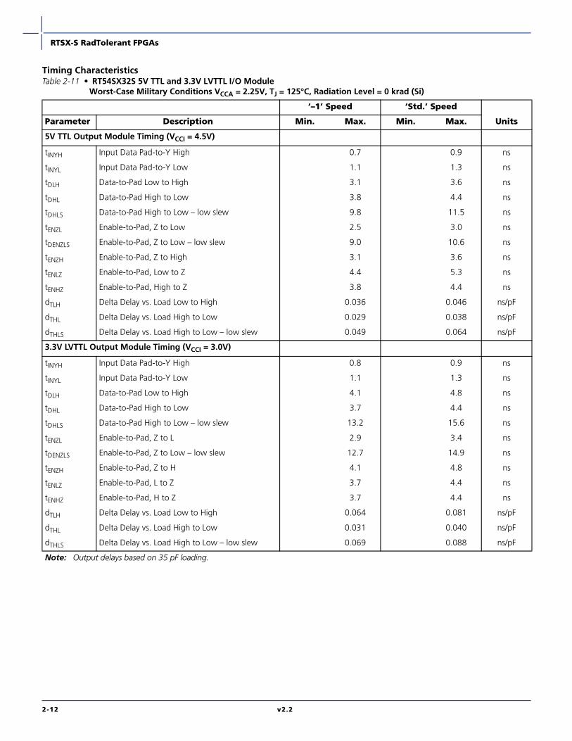
Timing Characteristics Table 2-11 • RT54SX32S 5V TTL and 3.3V LVTTL I/O Module
Worst-Case Military Conditions VCCA = 2.25V, TJ = 125°C, Radiation Level = 0 krad (Si)
‘–1’ Speed ‘Std.’ Speed
UnitsParameter Description Min. Max. Min. Max.
5V TTL Output Module Timing (VCCI = 4.5V)
tINYH Input Data Pad-to-Y High 0.7 0.9 ns
tINYL Input Data Pad-to-Y Low 1.1 1.3 ns
tDLH Data-to-Pad Low to High 3.1 3.6 ns
tDHL Data-to-Pad High to Low 3.8 4.4 ns
tDHLS Data-to-Pad High to Low – low slew 9.8 11.5 ns
tENZL Enable-to-Pad, Z to Low 2.5 3.0 ns
tDENZLS Enable-to-Pad, Z to Low – low slew 9.0 10.6 ns
tENZH Enable-to-Pad, Z to High 3.1 3.6 ns
tENLZ Enable-to-Pad, Low to Z 4.4 5.3 ns
tENHZ Enable-to-Pad, High to Z 3.8 4.4 ns
dTLH Delta Delay vs. Load Low to High 0.036 0.046 ns/pF
dTHL Delta Delay vs. Load High to Low 0.029 0.038 ns/pF
dTHLS Delta Delay vs. Load High to Low – low slew 0.049 0.064 ns/pF
3.3V LVTTL Output Module Timing (VCCI = 3.0V)
tINYH Input Data Pad-to-Y High 0.8 0.9 ns
tINYL Input Data Pad-to-Y Low 1.1 1.3 ns
tDLH Data-to-Pad Low to High 4.1 4.8 ns
tDHL Data-to-Pad High to Low 3.7 4.4 ns
tDHLS Data-to-Pad High to Low – low slew 13.2 15.6 ns
tENZL Enable-to-Pad, Z to L 2.9 3.4 ns
tDENZLS Enable-to-Pad, Z to Low – low slew 12.7 14.9 ns
tENZH Enable-to-Pad, Z to H 4.1 4.8 ns
tENLZ Enable-to-Pad, L to Z 3.7 4.4 ns
tENHZ Enable-to-Pad, H to Z 3.7 4.4 ns
dTLH Delta Delay vs. Load Low to High 0.064 0.081 ns/pF
dTHL Delta Delay vs. Load High to Low 0.031 0.040 ns/pF
dTHLS Delta Delay vs. Load High to Low – low slew 0.069 0.088 ns/pF
Note: Output delays based on 35 pF loading.
2-12 v2.2
RTSX-S RadTolerant FPGAs
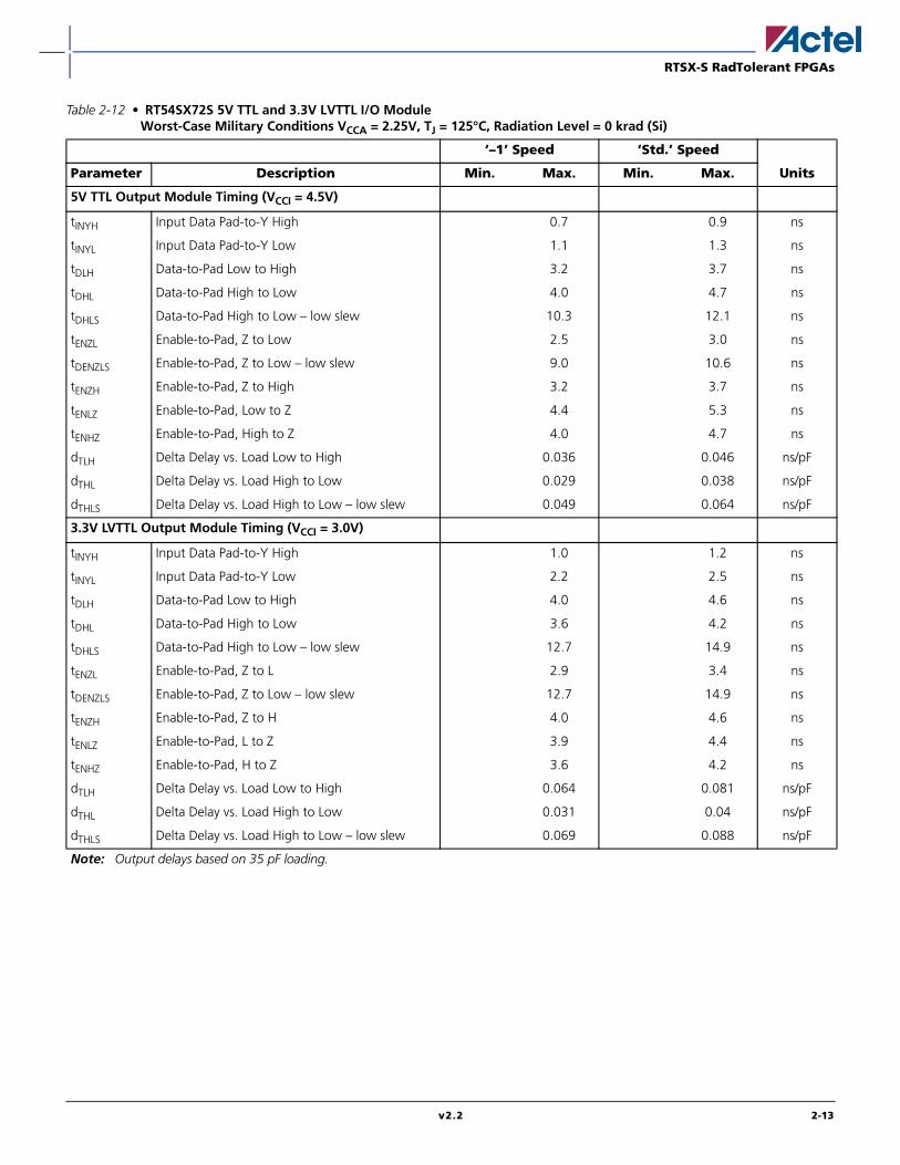
Table 2-12 • RT54SX72S 5V TTL and 3.3V LVTTL I/O ModuleWorst-Case Military Conditions VCCA = 2.25V, TJ = 125°C, Radiation Level = 0 krad (Si)
‘–1’ Speed ‘Std.’ Speed
UnitsParameter Description Min. Max. Min. Max.
5V TTL Output Module Timing (VCCI = 4.5V)
tINYH Input Data Pad-to-Y High 0.7 0.9 ns
tINYL Input Data Pad-to-Y Low 1.1 1.3 ns
tDLH Data-to-Pad Low to High 3.2 3.7 ns
tDHL Data-to-Pad High to Low 4.0 4.7 ns
tDHLS Data-to-Pad High to Low – low slew 10.3 12.1 ns
tENZL Enable-to-Pad, Z to Low 2.5 3.0 ns
tDENZLS Enable-to-Pad, Z to Low – low slew 9.0 10.6 ns
tENZH Enable-to-Pad, Z to High 3.2 3.7 ns
tENLZ Enable-to-Pad, Low to Z 4.4 5.3 ns
tENHZ Enable-to-Pad, High to Z 4.0 4.7 ns
dTLH Delta Delay vs. Load Low to High 0.036 0.046 ns/pF
dTHL Delta Delay vs. Load High to Low 0.029 0.038 ns/pF
dTHLS Delta Delay vs. Load High to Low – low slew 0.049 0.064 ns/pF
3.3V LVTTL Output Module Timing (VCCI = 3.0V)
tINYH Input Data Pad-to-Y High 1.0 1.2 ns
tINYL Input Data Pad-to-Y Low 2.2 2.5 ns
tDLH Data-to-Pad Low to High 4.0 4.6 ns
tDHL Data-to-Pad High to Low 3.6 4.2 ns
tDHLS Data-to-Pad High to Low – low slew 12.7 14.9 ns
tENZL Enable-to-Pad, Z to L 2.9 3.4 ns
tDENZLS Enable-to-Pad, Z to Low – low slew 12.7 14.9 ns
tENZH Enable-to-Pad, Z to H 4.0 4.6 ns
tENLZ Enable-to-Pad, L to Z 3.9 4.4 ns
tENHZ Enable-to-Pad, H to Z 3.6 4.2 ns
dTLH Delta Delay vs. Load Low to High 0.064 0.081 ns/pF
dTHL Delta Delay vs. Load High to Low 0.031 0.04 ns/pF
dTHLS Delta Delay vs. Load High to Low – low slew 0.069 0.088 ns/pF
Note: Output delays based on 35 pF loading.
v2.2 2-13
RTSX-S RadTolerant FPGAs
5V CMOS
Timing Characteristics
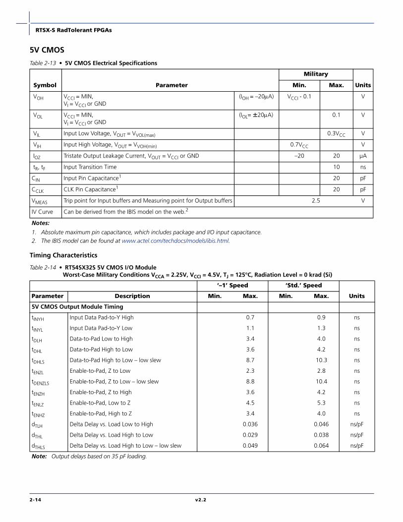
Table 2-13 • 5V CMOS Electrical Specifications
Symbol
Military
UnitsParameter Min. Max.
VOH VCCI = MIN,VI = VCCI or GND
(IOH = –20µA) VCCI - 0.1 V
VOL VCCI = MIN,VI = VCCI or GND
(IOL= ±20µA) 0.1 V
VIL Input Low Voltage, VOUT = VVOL(max) 0.3VCC V
VIH Input High Voltage, VOUT = VVOH(min) 0.7VCC V
IOZ Tristate Output Leakage Current, VOUT = VCCI or GND –20 20 µA
tR, tF Input Transition Time 10 ns
CIN Input Pin Capacitance1 20 pF
CCLK CLK Pin Capacitance1 20 pF
VMEAS Trip point for Input buffers and Measuring point for Output buffers 2.5 V
IV Curve Can be derived from the IBIS model on the web.2
Notes:
1. Absolute maximum pin capacitance, which includes package and I/O input capacitance.2. The IBIS model can be found at www.actel.com/techdocs/models/ibis.html.
Table 2-14 • RT54SX32S 5V CMOS I/O ModuleWorst-Case Military Conditions VCCA = 2.25V, VCCI = 4.5V, TJ = 125°C, Radiation Level = 0 krad (Si)
‘–1’ Speed ‘Std.’ Speed
UnitsParameter Description Min. Max. Min. Max.
5V CMOS Output Module Timing
tINYH Input Data Pad-to-Y High 0.7 0.9 ns
tINYL Input Data Pad-to-Y Low 1.1 1.3 ns
tDLH Data-to-Pad Low to High 3.4 4.0 ns
tDHL Data-to-Pad High to Low 3.6 4.2 ns
tDHLS Data-to-Pad High to Low – low slew 8.7 10.3 ns
tENZL Enable-to-Pad, Z to Low 2.3 2.8 ns
tDENZLS Enable-to-Pad, Z to Low – low slew 8.8 10.4 ns
tENZH Enable-to-Pad, Z to High 3.6 4.2 ns
tENLZ Enable-to-Pad, Low to Z 4.5 5.3 ns
tENHZ Enable-to-Pad, High to Z 3.4 4.0 ns
dTLH Delta Delay vs. Load Low to High 0.036 0.046 ns/pF
dTHL Delta Delay vs. Load High to Low 0.029 0.038 ns/pF
dTHLS Delta Delay vs. Load High to Low – low slew 0.049 0.064 ns/pF
Note: Output delays based on 35 pF loading.
2-14 v2.2
RTSX-S RadTolerant FPGAs
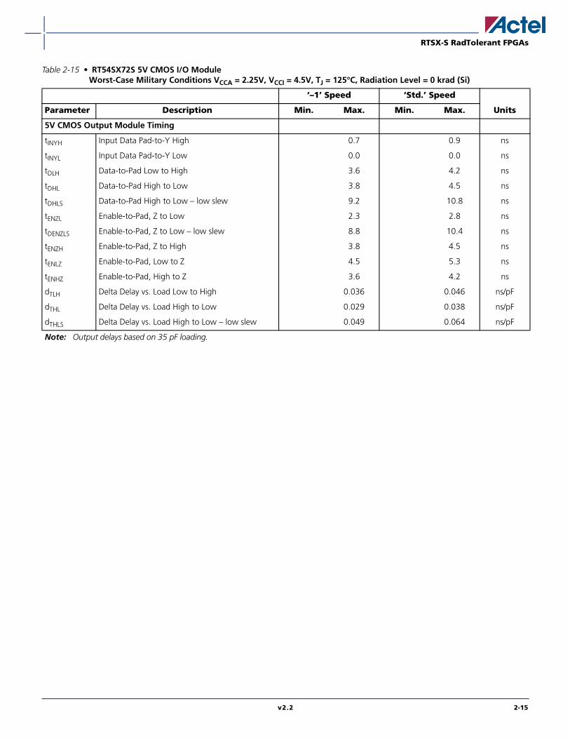
Table 2-15 • RT54SX72S 5V CMOS I/O ModuleWorst-Case Military Conditions VCCA = 2.25V, VCCI = 4.5V, TJ = 125°C, Radiation Level = 0 krad (Si)
‘–1’ Speed ‘Std.’ Speed
UnitsParameter Description Min. Max. Min. Max.
5V CMOS Output Module Timing
tINYH Input Data Pad-to-Y High 0.7 0.9 ns
tINYL Input Data Pad-to-Y Low 0.0 0.0 ns
tDLH Data-to-Pad Low to High 3.6 4.2 ns
tDHL Data-to-Pad High to Low 3.8 4.5 ns
tDHLS Data-to-Pad High to Low – low slew 9.2 10.8 ns
tENZL Enable-to-Pad, Z to Low 2.3 2.8 ns
tDENZLS Enable-to-Pad, Z to Low – low slew 8.8 10.4 ns
tENZH Enable-to-Pad, Z to High 3.8 4.5 ns
tENLZ Enable-to-Pad, Low to Z 4.5 5.3 ns
tENHZ Enable-to-Pad, High to Z 3.6 4.2 ns
dTLH Delta Delay vs. Load Low to High 0.036 0.046 ns/pF
dTHL Delta Delay vs. Load High to Low 0.029 0.038 ns/pF
dTHLS Delta Delay vs. Load High to Low – low slew 0.049 0.064 ns/pF
Note: Output delays based on 35 pF loading.
v2.2 2-15
RTSX-S RadTolerant FPGAs
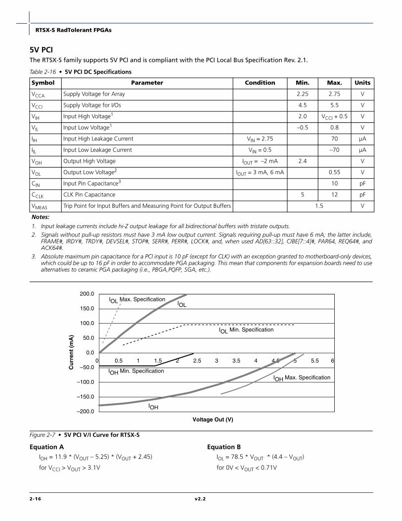
5V PCI The RTSX-S family supports 5V PCI and is compliant with the PCI Local Bus Specification Rev. 2.1.
Equation AIOH = 11.9 * (VOUT – 5.25) * (VOUT + 2.45)
for VCCI > VOUT > 3.1V
Equation BIOL = 78.5 * VOUT * (4.4 – VOUT)
for 0V < VOUT < 0.71V
Table 2-16 • 5V PCI DC Specifications
Symbol Parameter Condition Min. Max. Units
VCCA Supply Voltage for Array 2.25 2.75 V
VCCI Supply Voltage for I/Os 4.5 5.5 V
VIH Input High Voltage1 2.0 VCCI + 0.5 V
VIL Input Low Voltage1 –0.5 0.8 V
IIH Input High Leakage Current VIN = 2.75 70 µA
IIL Input Low Leakage Current VIN = 0.5 –70 µA
VOH Output High Voltage IOUT = –2 mA 2.4 V
VOL Output Low Voltage2 IOUT = 3 mA, 6 mA 0.55 V
CIN Input Pin Capacitance3 10 pF
CCLK CLK Pin Capacitance 5 12 pF
VMEAS Trip Point for Input Buffers and Measuring Point for Output Buffers 1.5 V
Notes:
1. Input leakage currents include hi-Z output leakage for all bidirectional buffers with tristate outputs.2. Signals without pull-up resistors must have 3 mA low output current. Signals requiring pull-up must have 6 mA; the latter include,
FRAME#, IRDY#, TRDY#, DEVSEL#, STOP#, SERR#, PERR#, LOCK#, and, when used AD[63::32], C/BE[7::4]#, PAR64, REQ64#, andACK64#.
3. Absolute maximum pin capacitance for a PCI input is 10 pF (except for CLK) with an exception granted to motherboard-only devices,which could be up to 16 pF in order to accommodate PGA packaging. This mean that components for expansion boards need to usealternatives to ceramic PGA packaging (i.e., PBGA,PQFP, SGA, etc.).
Figure 2-7 • 5V PCI V/I Curve for RTSX-S
–200.0
–150.0
–100.0
–50.0
0.0
50.0
100.0
150.0
200.0
0 0.5 1 1.5 2 2.5 3 3.5 4 4.5 5 5.5 6
Voltage Out (V)
Cu
rren
t (m
A)
IOH
IOL
IOH Min. SpecificationIOH Max. Specification
IOL Min. Specification
IOL Max. Specification
2-16 v2.2
RTSX-S RadTolerant FPGAs
Table 2-17 • 5V PCI AC Specifications
Symbol Parameter Condition Min. Max. Units
IOH(AC) 0 < VOUT < 1.4 1 –44 mA
Switching Current High 1.4 < VOUT < 2.4 1, 2 (–44 + (VOUT – 1.4)/0.024) mA
3.1 < VOUT < VCCI 1, 3 "Equation A" on
page 2-16
(Test Point) VOUT = 3.1 3 –142 mA
IOL(AC) VOUT = 2.2 1 95 mA
Switching Current Low 2.2 > VOUT > 0.55 1 (VOUT/0.023) mA
0.71 > VOUT > 0 1, 3 "Equation B" on page 2-16
(Test Point) VOUT = 0.71 206 mA
ICL Low Clamp Current –5 < VIN ≤ –1 –25 + (VIN + 1)/0.015 mA
slewR Output Rise Slew Rate 0.4V to 2.4V load4 1 5 V/ns
slewF Output Fall Slew Rate 2.4V to 0.4V load4 1 5 V/ns
Notes:
1. Refer to the V/I curves in Figure 2-7 on page 2-16. Switching current characteristics for REQ# and GNT# are permitted to be onehalf of that specified here; i.e., half size output drivers may be used on these signals. This specification does not apply to CLK andRST#, which are system outputs. The “Switching Current High” specification is not relevant to SERR#, INTA#, INTB#, INTC#, andINTD#, which are open drain outputs.
2. Note that this segment of the minimum current curve is drawn from the AC drive point directly to the DC drive point rather thantoward the voltage rail (as is done in the pull-down curve). This difference is intended to allow for an optional N-channel pull-up.
3. Maximum current requirements must be met as drivers pull beyond the last step voltage. Equations defining these maximums (Aand B) are provided with the respective curves in Figure 2-7 on page 2-16. The equation defined maximum should be met by thedesign. In order to facilitate component testing, a maximum current test point is defined for each side of the output driver.
4. This parameter is to be interpreted as the cumulative edge rate across the specified range, rather than the instantaneous rate at anypoint within the transition range. The specified load is optional; i.e., the designer may elect to meet this parameter with anunloaded output per revision 2.0 of the PCI Local Bus Specification (Figure 2-8). However, adherence to both the maximum andminimum parameters is now required (the maximum is no longer simply a guideline). Since adherence to the maximum slew ratewas not required prior to revision 2.1 of the specification, there may be components in the market that have faster edge rates;therefore, motherboard designers must bear in mind that rise and fall times faster than this specification could occur and shouldensure that signal integrity modeling accounts for this. Rise slew rate does not apply to open drain outputs.
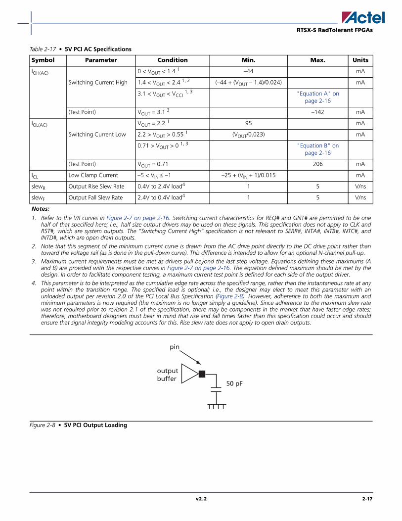
Figure 2-8 • 5V PCI Output Loading
pin
outputbuffer
50 pF
v2.2 2-17
RTSX-S RadTolerant FPGAs
Timing Characteristics Table 2-18 • RT54SX32S 5V PCI I/O Module
Worst-Case Military Conditions VCCA = 2.25V, VCCI = 4.5V, TJ= 125°C, Radiation Level = 0 krad (Si)
‘–1’ Speed ‘Std.’ Speed
UnitsParameter Description Min. Max. Min. Max.
5V PCI Output Module Timing
tINYH Input Data Pad-to-Y High 0.7 0.9 ns
tINYL Input Data Pad-to-Y Low 1.1 1.3 ns
tDLH Data-to-Pad Low to High 3.4 4.0 ns
tDHL Data-to-Pad High to Low 4.1 4.8 ns
tENZL Enable-to-Pad, Z to Low 2.8 3.3 ns
tENZH Enable-to-Pad, Z to High 3.4 4.0 ns
tENLZ Enable-to-Pad, Low to Z 4.9 5.8 ns
tENHZ Enable-to-Pad, High to Z 4.1 4.8 ns
dTLH Delta Delay vs. Load Low to High 0.036 0.046 ns/pF
dTHL Delta Delay vs. Load High to Low 0.029 0.038 ns/pF
Note: Output delays based on 50 pF loading.
Table 2-19 • RT54SX72S 5V PCI I/O ModuleWorst-Case Military Conditions VCCA = 2.25V, VCCI = 4.5V, TJ= 125°C, Radiation Level = 0 krad (Si)
‘–1’ Speed ‘Std.’ Speed
UnitsParameter Description Min. Max. Min. Max.
5V PCI Output Module Timing
tINYH Input Data Pad-to-Y High 0.7 0.9 ns
tINYL Input Data Pad-to-Y Low 1.1 1.3 ns
tDLH Data-to-Pad Low to High 3.5 4.1 ns
tDHL Data-to-Pad High to Low 4.3 5.1 ns
tENZL Enable-to-Pad, Z to Low 2.8 3.3 ns
tENZH Enable-to-Pad, Z to High 3.5 4.1 ns
tENLZ Enable-to-Pad, Low to Z 4.9 5.8 ns
tENHZ Enable-to-Pad, High to Z 4.3 5.1 ns
dTLH Delta Delay vs. Load Low to High 0.036 0.046 ns/pF
dTHL Delta Delay vs. Load High to Low 0.029 0.038 ns/pF
Note: Output delays based on 50 pF loading.
2-18 v2.2
RTSX-S RadTolerant FPGAs
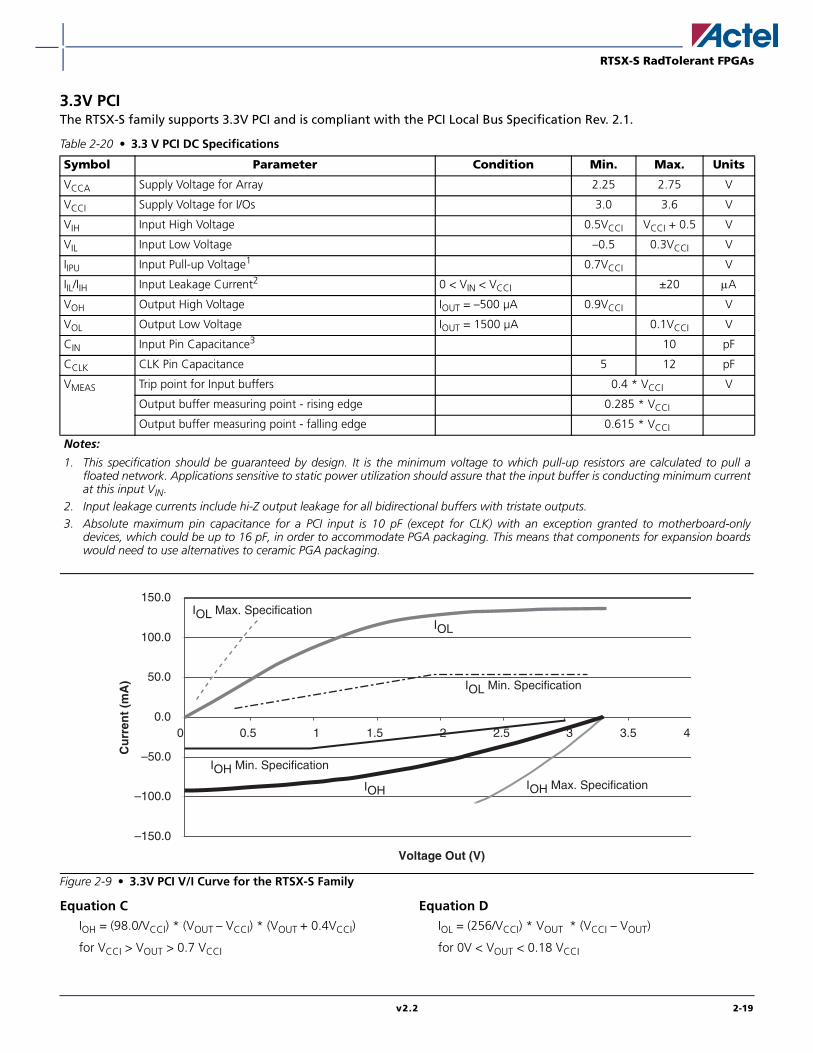
3.3V PCIThe RTSX-S family supports 3.3V PCI and is compliant with the PCI Local Bus Specification Rev. 2.1.
Equation CIOH = (98.0/VCCI) * (VOUT – VCCI) * (VOUT + 0.4VCCI)
for VCCI > VOUT > 0.7 VCCI
Equation DIOL = (256/VCCI) * VOUT * (VCCI – VOUT)
for 0V < VOUT < 0.18 VCCI
Table 2-20 • 3.3 V PCI DC Specifications
Symbol Parameter Condition Min. Max. Units
VCCA Supply Voltage for Array 2.25 2.75 V
VCCI Supply Voltage for I/Os 3.0 3.6 V
VIH Input High Voltage 0.5VCCI VCCI + 0.5 V
VIL Input Low Voltage –0.5 0.3VCCI V
IIPU Input Pull-up Voltage1 0.7VCCI V
IIL/IIH Input Leakage Current2 0 < VIN < VCCI ±20 µA
VOH Output High Voltage IOUT = –500 µA 0.9VCCI V
VOL Output Low Voltage IOUT = 1500 µA 0.1VCCI V
CIN Input Pin Capacitance3 10 pF
CCLK CLK Pin Capacitance 5 12 pF
VMEAS Trip point for Input buffers 0.4 * VCCI V
Output buffer measuring point - rising edge 0.285 * VCCI
Output buffer measuring point - falling edge 0.615 * VCCI
Notes:
1. This specification should be guaranteed by design. It is the minimum voltage to which pull-up resistors are calculated to pull afloated network. Applications sensitive to static power utilization should assure that the input buffer is conducting minimum currentat this input VIN.
2. Input leakage currents include hi-Z output leakage for all bidirectional buffers with tristate outputs.3. Absolute maximum pin capacitance for a PCI input is 10 pF (except for CLK) with an exception granted to motherboard-only
devices, which could be up to 16 pF, in order to accommodate PGA packaging. This means that components for expansion boardswould need to use alternatives to ceramic PGA packaging.
Figure 2-9 • 3.3V PCI V/I Curve for the RTSX-S Family
–150.0
–100.0
–50.0
0.0
50.0
100.0
150.0
0 0.5 1 1.5 2 2.5 3 3.5 4
Voltage Out (V)
Cu
rren
t (m
A)
IOH
IOL
IOH Min. Specification
IOH Max. Specification
IOL Min. Specification
IOL Max. Specification
v2.2 2-19
RTSX-S RadTolerant FPGAs
Table 2-21 • 3.3V PCI AC Specifications
Symbol Parameter Condition Min. Max. Units
IOH(AC) Switching Current High 0 < VOUT ≤ 0.3VCCI 1 –12VCCI mA
0.3VCCI ≤ VOUT < 0.9VCCI 1 (–17.1 + (VCCI – VOUT)) mA
0.7VCCI < VOUT < VCCI 1, 2 "Equation C" on
page 2-19
(Test Point) VOUT = 0.7VCC 2 –32VCCI mA
IOL(AC) Switching Current Low VCCI > VOUT ≥ 0.6VCCI 1 16VCCI mA
0.6VCCI > VOUT > 0.1VCCI 1 (26.7VOUT) mA
0.18VCCI > VOUT > 0 1, 2 "Equation D" on page 2-19
(Test Point) VOUT = 0.18VCC 2 38VCCI mA
ICL Low Clamp Current –3 < VIN ≤ –1 –25 + (VIN + 1)/0.015 mA
ICH High Clamp Current VCCI + 4 > VIN ≥ VCCI + 1 25 + (VIN – VCCI – 1)/0.015 mA
slewR Output Rise Slew Rate 0.2VCCI to 0.6VCCI load 3 1 4 V/ns
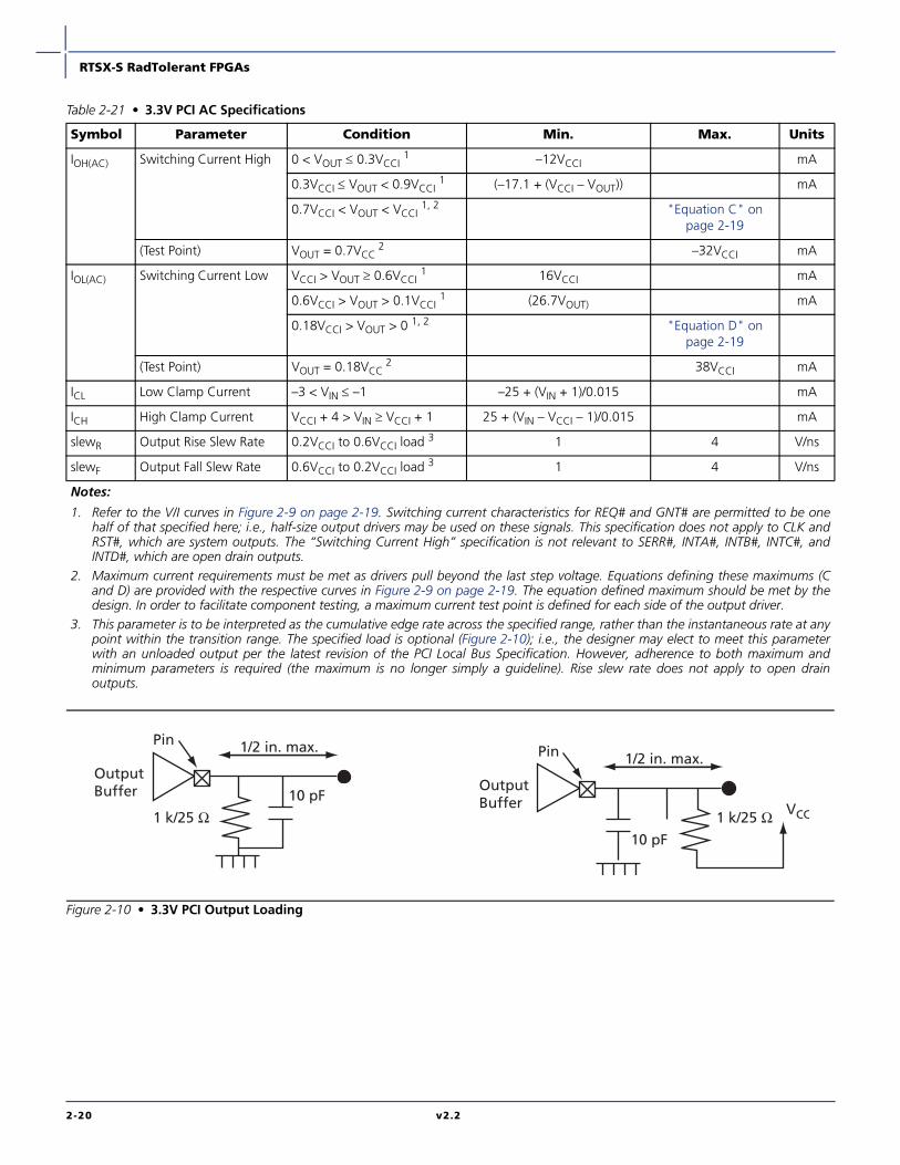
slewF Output Fall Slew Rate 0.6VCCI to 0.2VCCI load 3 1 4 V/ns
Notes:
1. Refer to the V/I curves in Figure 2-9 on page 2-19. Switching current characteristics for REQ# and GNT# are permitted to be onehalf of that specified here; i.e., half-size output drivers may be used on these signals. This specification does not apply to CLK andRST#, which are system outputs. The “Switching Current High” specification is not relevant to SERR#, INTA#, INTB#, INTC#, andINTD#, which are open drain outputs.
2. Maximum current requirements must be met as drivers pull beyond the last step voltage. Equations defining these maximums (Cand D) are provided with the respective curves in Figure 2-9 on page 2-19. The equation defined maximum should be met by thedesign. In order to facilitate component testing, a maximum current test point is defined for each side of the output driver.
3. This parameter is to be interpreted as the cumulative edge rate across the specified range, rather than the instantaneous rate at anypoint within the transition range. The specified load is optional (Figure 2-10); i.e., the designer may elect to meet this parameterwith an unloaded output per the latest revision of the PCI Local Bus Specification. However, adherence to both maximum andminimum parameters is required (the maximum is no longer simply a guideline). Rise slew rate does not apply to open drainoutputs.
Figure 2-10 • 3.3V PCI Output Loading
Pin
OutputBuffer
1 k/25 Ω
1/2 in. max.
10 pF
Pin
OutputBuffer
1 k/25 Ω
1/2 in. max.
10 pF
VCC
2-20 v2.2
RTSX-S RadTolerant FPGAs
Timing Characteristics
Table 2-22 • RT54SX32S 3.3V PCI I/O ModuleWorst-Case Military Conditions VCCA = 2.25V, VCCI = 3.0V, TJ = 125°C, Radiation Level = 0 krad (Si)
‘–1’ Speed ‘Std.’ Speed
UnitsParameter Description Min. Max. Min. Max.
3.3V PCI Output Module Timing
tINYH Input Data Pad-to-Y High 0.8 0.9 ns
tINYL Input Data Pad-to-Y Low 0.9 1.1 ns
tDLH Data-to-Pad Low to High 3.0 3.5 ns
tDHL Data-to-Pad High to Low 3.0 3.5 ns
tENZL Enable-to-Pad, Z to Low 2.1 2.5 ns
tENZH Enable-to-Pad, Z to High 3.0 3.5 ns
tENLZ Enable-to-Pad, Low to Z 2.7 3.9 ns
tENHZ Enable-to-Pad, High to Z 3.0 3.5 ns
dTLH Delta Delay vs. Load Low to High 0.067 0.085 ns/pF
dTHL Delta Delay vs. Load High to Low 0.031 0.040 ns/pF
Note: Delays based on 10 pF loading and 25 Ω resistance.
Table 2-23 • RT54SX72S 3.3V PCI I/O ModuleWorst-Case Military Conditions VCCA = 2.25V, VCCI = 3.0V, TJ = 125°C, Radiation Level = 0 krad (Si)
‘–1’ Speed ‘Std.’ Speed
UnitsParameter Description Min. Max. Min. Max.
3.3V PCI Output Module Timing
tINYH Input Data Pad-to-Y High 0.7 0.8 ns
tINYL Input Data Pad-to-Y Low 0.9 1.1 ns
tDLH Data-to-Pad Low to High 2.8 3.3 ns
tDHL Data-to-Pad High to Low 2.8 3.3 ns
tENZL Enable-to-Pad, Z to Low 2.1 2.5 ns
tENZH Enable-to-Pad, Z to High 2.8 3.3 ns
tENLZ Enable-to-Pad, Low to Z 2.7 3.9 ns
tENHZ Enable-to-Pad, High to Z 2.8 3.3 ns
dTLH Delta Delay vs. Load Low to High 0.067 0.085 ns/pF
dTHL Delta Delay vs. Load High to Low 0.031 0.040 ns/pF
Note: Delays based on 10 pF loading and 25 Ω resistance.
v2.2 2-21
RTSX-S RadTolerant FPGAs
Module Specifications
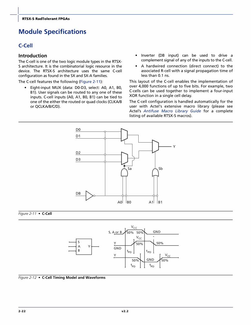
C-Cell
IntroductionThe C-cell is one of the two logic module types in the RTSX-S architecture. It is the combinatorial logic resource in thedevice. The RTSX-S architecture uses the same C-cellconfiguration as found in the SX and SX-A families.
The C-cell features the following (Figure 2-11):
• Eight-input MUX (data: D0-D3, select: A0, A1, B0,B1). User signals can be routed to any one of theseinputs. C-cell inputs (A0, A1, B0, B1) can be tied toone of the either the routed or quad clocks (CLKA/Bor QCLKA/B/C/D).
• Inverter (DB input) can be used to drive acomplement signal of any of the inputs to the C-cell.
• A hardwired connection (direct connect) to theassociated R-cell with a signal propagation time ofless than 0.1 ns.
This layout of the C-cell enables the implementation ofover 4,000 functions of up to five bits. For example, twoC-cells can be used together to implement a four-inputXOR function in a single cell delay.
The C-cell configuration is handled automatically for theuser with Actel's extensive macro library (please seeActel’s Antifuse Macro Library Guide for a completelisting of available RTSX-S macros).
Figure 2-11 • C-Cell
Figure 2-12 • C-Cell Timing Model and Waveforms
D0
D1
D2
D3
DB
A0 B0 A1 B1
Sa Sb
Y
SAB
Y
S, A or B
Y
GND
VCC
50%
tPD
Y
GND
GND
VCC
50%
50% 50%
VCC
50% 50%tPD
tPDtPD
2-22 v2.2
RTSX-S RadTolerant FPGAs
Timing Characteristics
R-Cell
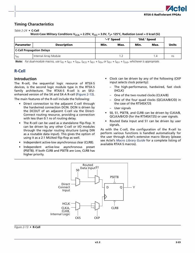
IntroductionThe R-cell, the sequential logic resource of RTSX-Sdevices, is the second logic module type in the RTSX-Sfamily architecture. The RTAX-S R-cell is an SEU-enhanced version of the SX and SX-A R-cell (Figure 2-13).
The main features of the R-cell include the following:
• Direct connection to the adjacent C-cell throughthe hardwired connection DCIN. DCIN is driven bythe DCOUT of an adjacent C-cell via the Direct-Connect routing resource, providing a connectionwith less than 0.1 ns of routing delay.
• The R-cell can be used as a standalone flip-flop. Itcan be driven by any other C-cell or I/O modulesthrough the regular routing structure (using DINas a routable data input). This gives the option ofusing it as a 2:1 MUXed flip-flop as well.
• Independent active-low asynchronous clear (CLRB).
• Independent active-low asynchronous preset(PSETB). If both CLRB and PSETB are Low, CLRB hashigher priority.
• Clock can be driven by any of the following (CKPinput selects clock polarity):
– The high-performance, hardwired, fast clock(HCLK)
– One of the two routed clocks (CLKA/B)
– One of the four quad clocks (QCLKA/B/C/D) inthe case of the RT54SX72S
– User signals
• S0, S1, PSETB, and CLRB can be driven by CLKA/B,QCLKA/B/C/D (for the RT54SX72S) or user signals.
• Routed Data Input and S1 can be driven by usersignals.
As with the C-cell, the configuration of the R-cell toperform various functions is handled automatically forthe user through Actel's extensive macro library (pleasesee Actel’s Macro Library Guide for a complete listing ofavailable RTAX-S macros).
Table 2-24 • C-CellWorst-Case Military Conditions VCCA = 2.25V, VCCI = 3.0V, TJ= 125°C, Radiation Level = 0 krad (Si)
‘–1’ Speed ‘Std.’ Speed
UnitsParameter Description Min. Max. Min. Max.
C-Cell Propagation Delays
tPD Internal Array Module 1.2 1.4 ns
Note: For dual-module macros, use tPD + tRD1 + tPDn, tRCO + tRD1 + tPDn or tPD1 + tRD1 + tSUD, whichever is appropriate.
Figure 2-13 • R-Cell
DirectConnect
Input
CLKA,CLKB,
Internal Logic
HCLK
CKS CKP
CLRB
PSETB
YD Q
RoutedData Input
S0S1
v2.2 2-23
RTSX-S RadTolerant FPGAs
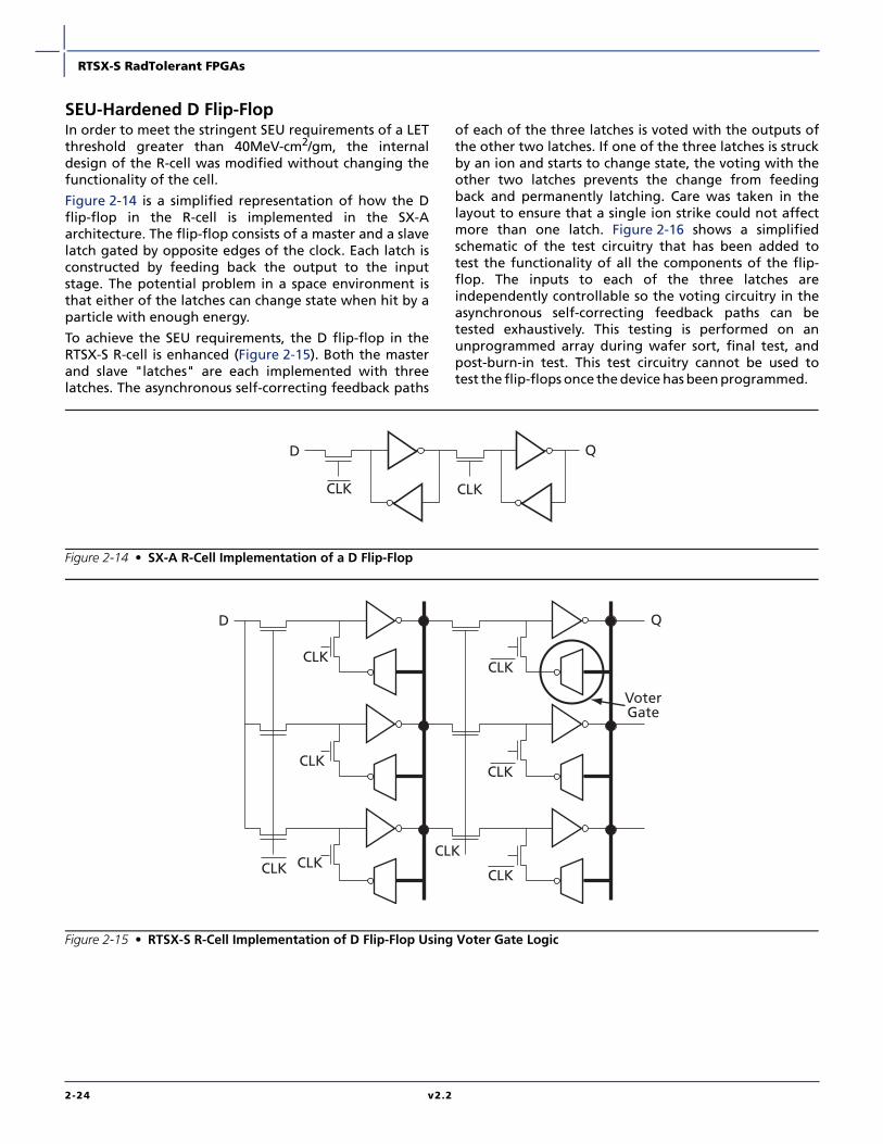
SEU-Hardened D Flip-FlopIn order to meet the stringent SEU requirements of a LETthreshold greater than 40MeV-cm2/gm, the internaldesign of the R-cell was modified without changing thefunctionality of the cell.
Figure 2-14 is a simplified representation of how the Dflip-flop in the R-cell is implemented in the SX-Aarchitecture. The flip-flop consists of a master and a slavelatch gated by opposite edges of the clock. Each latch isconstructed by feeding back the output to the inputstage. The potential problem in a space environment isthat either of the latches can change state when hit by aparticle with enough energy.
To achieve the SEU requirements, the D flip-flop in theRTSX-S R-cell is enhanced (Figure 2-15). Both the masterand slave "latches" are each implemented with threelatches. The asynchronous self-correcting feedback paths
of each of the three latches is voted with the outputs ofthe other two latches. If one of the three latches is struckby an ion and starts to change state, the voting with theother two latches prevents the change from feedingback and permanently latching. Care was taken in thelayout to ensure that a single ion strike could not affectmore than one latch. Figure 2-16 shows a simplifiedschematic of the test circuitry that has been added totest the functionality of all the components of the flip-flop. The inputs to each of the three latches areindependently controllable so the voting circuitry in theasynchronous self-correcting feedback paths can betested exhaustively. This testing is performed on anunprogrammed array during wafer sort, final test, andpost-burn-in test. This test circuitry cannot be used totest the flip-flops once the device has been programmed.
Figure 2-14 • SX-A R-Cell Implementation of a D Flip-Flop
Figure 2-15 • RTSX-S R-Cell Implementation of D Flip-Flop Using Voter Gate Logic
D
CLK CLK
Q
CLKCLK
D
CLK
Q
VoterGate
CLK
CLK
CLK
CLK
CLK
2-24 v2.2
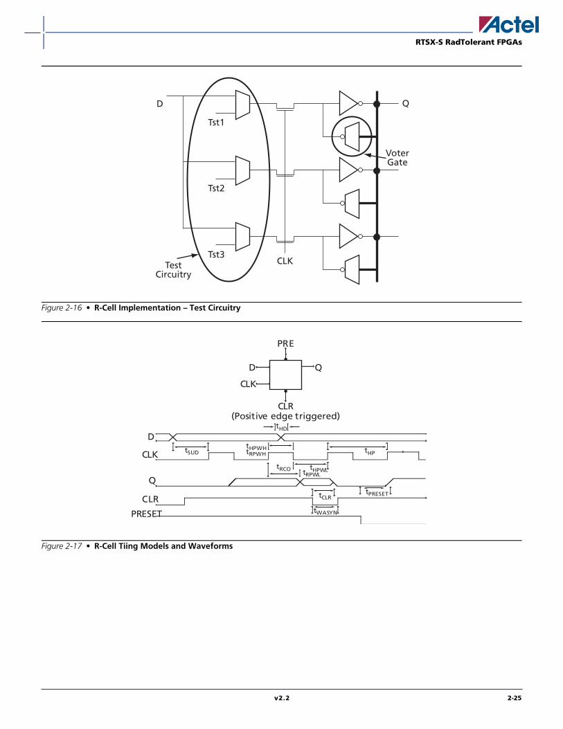
RTSX-S RadTolerant FPGAs
Figure 2-16 • R-Cell Implementation – Test Circuitry
Figure 2-17 • R-Cell Tiing Models and Waveforms
Tst1
CLK
D Q
VoterGate
Tst2
Tst3Test
Circuitry
(Positive edge triggered)
D
CLK
CLR
Q
D
CLK
Q
CLR
tHPWH
RCO
tWASYN
tSUD
tHPWLt
tCLR
tRPWL
tRPWH
PRESET
tPRESET
PRE
tHD
tHP
v2.2 2-25
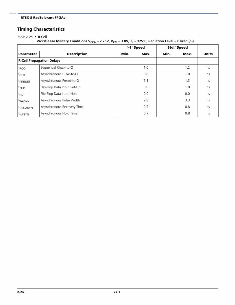
RTSX-S RadTolerant FPGAs
Timing Characteristics
Table 2-25 • R-CellWorst-Case Military Conditions VCCA = 2.25V, VCCI = 3.0V, TJ = 125°C, Radiation Level = 0 krad (Si)
‘–1’ Speed ‘Std.’ Speed
UnitsParameter Description Min. Max. Min. Max.
R-Cell Propagation Delays
tRCO Sequential Clock-to-Q 1.0 1.2 ns
tCLR Asynchronous Clear-to-Q 0.8 1.0 ns
tPRESET Asynchronous Preset-to-Q 1.1 1.3 ns
tSUD Flip-Flop Data Input Set-Up 0.8 1.0 ns
tHD Flip-Flop Data Input Hold 0.0 0.0 ns
tWASYN Asynchronous Pulse Width 2.8 3.3 ns
tRECASYN Asynchronous Recovery Time 0.7 0.8 ns
tHASYN Asynchronous Hold Time 0.7 0.8 ns
2-26 v2.2
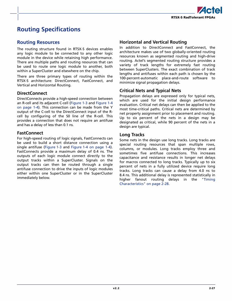
RTSX-S RadTolerant FPGAs
Routing Specifications
Routing ResourcesThe routing structure found in RTSX-S devices enablesany logic module to be connected to any other logicmodule in the device while retaining high performance.There are multiple paths and routing resources that canbe used to route one logic module to another, bothwithin a SuperCluster and elsewhere on the chip.
There are three primary types of routing within theRTSX-S architecture: DirectConnect, FastConnect, andVertical and Horizontal Routing.
DirectConnectDirectConnects provide a high-speed connection betweenan R-cell and its adjacent C-cell (Figure 1-3 and Figure 1-4on page 1-4). This connection can be made from the Youtput of the C-cell to the DirectConnect input of the R-cell by configuring of the S0 line of the R-cell. Thisprovides a connection that does not require an antifuseand has a delay of less than 0.1 ns.
FastConnectFor high-speed routing of logic signals, FastConnects canbe used to build a short distance connection using asingle antifuse (Figure 1-3 and Figure 1-4 on page 1-4).FastConnects provide a maximum delay of 0.4 ns. Theoutputs of each logic module connect directly to theoutput tracks within a SuperCluster. Signals on theoutput tracks can then be routed through a singleantifuse connection to drive the inputs of logic moduleseither within one SuperCluster or in the SuperClusterimmediately below.
Horizontal and Vertical RoutingIn addition to DirectConnect and FastConnect, thearchitecture makes use of two globally-oriented routingresources known as segmented routing and high-driverouting. Actel’s segmented routing structure provides avariety of track lengths for extremely fast routingbetween SuperClusters. The exact combination of tracklengths and antifuses within each path is chosen by the100-percent-automatic place-and-route software tominimize signal propagation delays.
Critical Nets and Typical NetsPropagation delays are expressed only for typical nets,which are used for the initial design performanceevaluation. Critical net delays can then be applied to themost time-critical paths. Critical nets are determined bynet property assignment prior to placement and routing.Up to six percent of the nets in a design may bedesignated as critical, while 90 percent of the nets in adesign are typical.
Long TracksSome nets in the design use long tracks. Long tracks arespecial routing resources that span multiple rows,columns, or modules. Long tracks employ three andsometimes five antifuse connections. This increasescapacitance and resistance results in longer net delaysfor macros connected to long tracks. Typically up to sixpercent of nets in a fully utilized device require longtracks. Long tracks can cause a delay from 4.0 ns to8.4 ns. This additional delay is represented statistically inhigher fanout routing delays in the "TimingCharacteristics" on page 2-28.
v2.2 2-27
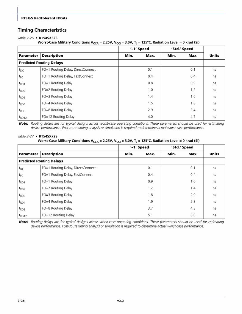
RTSX-S RadTolerant FPGAs
Timing Characteristics Table 2-26 • RT54SX32S
Worst-Case Military Conditions VCCA = 2.25V, VCCI = 3.0V, TJ = 125°C, Radiation Level = 0 krad (Si)
‘–1’ Speed ‘Std.’ Speed
UnitsParameter Description Min. Max. Min. Max.
Predicted Routing Delays
tDC FO=1 Routing Delay, DirectConnect 0.1 0.1 ns
tFC FO=1 Routing Delay, FastConnect 0.4 0.4 ns
tRD1 FO=1 Routing Delay 0.8 0.9 ns
tRD2 FO=2 Routing Delay 1.0 1.2 ns
tRD3 FO=3 Routing Delay 1.4 1.6 ns
tRD4 FO=4 Routing Delay 1.5 1.8 ns
tRD8 FO=8 Routing Delay 2.9 3.4 ns
tRD12 FO=12 Routing Delay 4.0 4.7 ns
Note: Routing delays are for typical designs across worst-case operating conditions. These parameters should be used for estimatingdevice performance. Post-route timing analysis or simulation is required to determine actual worst-case performance.
Table 2-27 • RT54SX72S Worst-Case Military Conditions VCCA = 2.25V, VCCI = 3.0V, TJ = 125°C, Radiation Level = 0 krad (Si)
‘–1’ Speed ‘Std.’ Speed
UnitsParameter Description Min. Max. Min. Max.
Predicted Routing Delays
tDC FO=1 Routing Delay, DirectConnect 0.1 0.1 ns
tFC FO=1 Routing Delay, FastConnect 0.4 0.4 ns
tRD1 FO=1 Routing Delay 0.9 1.0 ns
tRD2 FO=2 Routing Delay 1.2 1.4 ns
tRD3 FO=3 Routing Delay 1.8 2.0 ns
tRD4 FO=4 Routing Delay 1.9 2.3 ns
tRD8 FO=8 Routing Delay 3.7 4.3 ns
tRD12 FO=12 Routing Delay 5.1 6.0 ns
Note: Routing delays are for typical designs across worst-case operating conditions. These parameters should be used for estimatingdevice performance. Post-route timing analysis or simulation is required to determine actual worst-case performance.
2-28 v2.2
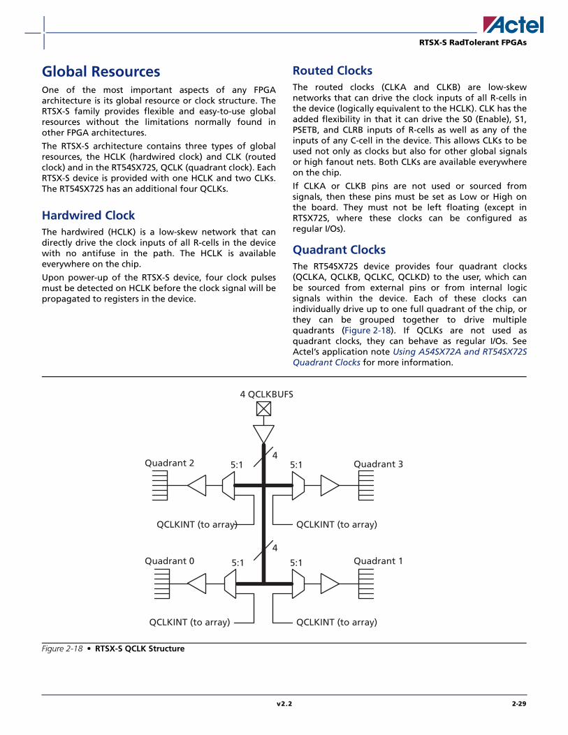
RTSX-S RadTolerant FPGAs
Global ResourcesOne of the most important aspects of any FPGAarchitecture is its global resource or clock structure. TheRTSX-S family provides flexible and easy-to-use globalresources without the limitations normally found inother FPGA architectures.
The RTSX-S architecture contains three types of globalresources, the HCLK (hardwired clock) and CLK (routedclock) and in the RT54SX72S, QCLK (quadrant clock). EachRTSX-S device is provided with one HCLK and two CLKs.The RT54SX72S has an additional four QCLKs.
Hardwired ClockThe hardwired (HCLK) is a low-skew network that candirectly drive the clock inputs of all R-cells in the devicewith no antifuse in the path. The HCLK is availableeverywhere on the chip.
Upon power-up of the RTSX-S device, four clock pulsesmust be detected on HCLK before the clock signal will bepropagated to registers in the device.
Routed ClocksThe routed clocks (CLKA and CLKB) are low-skewnetworks that can drive the clock inputs of all R-cells inthe device (logically equivalent to the HCLK). CLK has theadded flexibility in that it can drive the S0 (Enable), S1,PSETB, and CLRB inputs of R-cells as well as any of theinputs of any C-cell in the device. This allows CLKs to beused not only as clocks but also for other global signalsor high fanout nets. Both CLKs are available everywhereon the chip.
If CLKA or CLKB pins are not used or sourced fromsignals, then these pins must be set as Low or High onthe board. They must not be left floating (except inRTSX72S, where these clocks can be configured asregular I/Os).
Quadrant ClocksThe RT54SX72S device provides four quadrant clocks(QCLKA, QCLKB, QCLKC, QCLKD) to the user, which canbe sourced from external pins or from internal logicsignals within the device. Each of these clocks canindividually drive up to one full quadrant of the chip, orthey can be grouped together to drive multiplequadrants (Figure 2-18). If QCLKs are not used asquadrant clocks, they can behave as regular I/Os. SeeActel’s application note Using A54SX72A and RT54SX72SQuadrant Clocks for more information.
Figure 2-18 • RTSX-S QCLK Structure
4
4
4 QCLKBUFS
5:1 5:1
5:1 5:1
Quadrant 2
Quadrant 0
Quadrant 3
Quadrant 1
QCLKINT (to array)
QCLKINT (to array)
QCLKINT (to array)
QCLKINT (to array)
v2.2 2-29
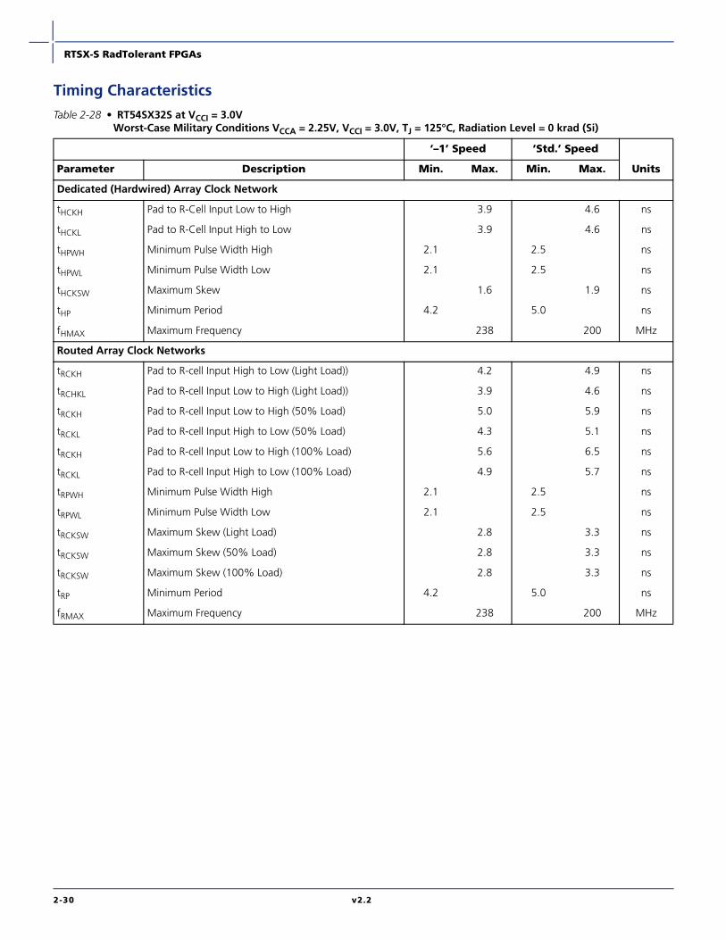
RTSX-S RadTolerant FPGAs
Timing Characteristics
Table 2-28 • RT54SX32S at VCCI = 3.0VWorst-Case Military Conditions VCCA = 2.25V, VCCI = 3.0V, TJ = 125°C, Radiation Level = 0 krad (Si)
‘–1’ Speed ‘Std.’ Speed
UnitsParameter Description Min. Max. Min. Max.
Dedicated (Hardwired) Array Clock Network
tHCKH Pad to R-Cell Input Low to High 3.9 4.6 ns
tHCKL Pad to R-Cell Input High to Low 3.9 4.6 ns
tHPWH Minimum Pulse Width High 2.1 2.5 ns
tHPWL Minimum Pulse Width Low 2.1 2.5 ns
tHCKSW Maximum Skew 1.6 1.9 ns
tHP Minimum Period 4.2 5.0 ns
fHMAX Maximum Frequency 238 200 MHz
Routed Array Clock Networks
tRCKH Pad to R-cell Input High to Low (Light Load)) 4.2 4.9 ns
tRCHKL Pad to R-cell Input Low to High (Light Load)) 3.9 4.6 ns
tRCKH Pad to R-cell Input Low to High (50% Load) 5.0 5.9 ns
tRCKL Pad to R-cell Input High to Low (50% Load) 4.3 5.1 ns
tRCKH Pad to R-cell Input Low to High (100% Load) 5.6 6.5 ns
tRCKL Pad to R-cell Input High to Low (100% Load) 4.9 5.7 ns
tRPWH Minimum Pulse Width High 2.1 2.5 ns
tRPWL Minimum Pulse Width Low 2.1 2.5 ns
tRCKSW Maximum Skew (Light Load) 2.8 3.3 ns
tRCKSW Maximum Skew (50% Load) 2.8 3.3 ns
tRCKSW Maximum Skew (100% Load) 2.8 3.3 ns
tRP Minimum Period 4.2 5.0 ns
fRMAX Maximum Frequency 238 200 MHz
2-30 v2.2
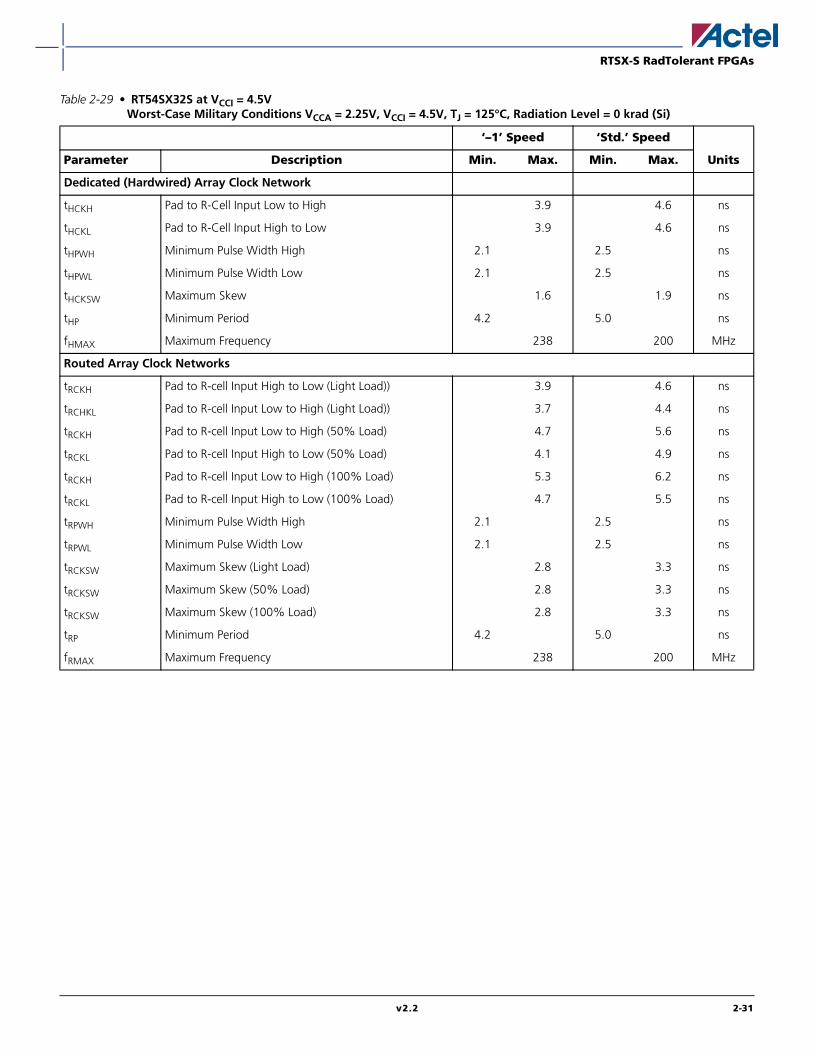
RTSX-S RadTolerant FPGAs
Table 2-29 • RT54SX32S at VCCI = 4.5VWorst-Case Military Conditions VCCA = 2.25V, VCCI = 4.5V, TJ = 125°C, Radiation Level = 0 krad (Si)
‘–1’ Speed ‘Std.’ Speed
UnitsParameter Description Min. Max. Min. Max.
Dedicated (Hardwired) Array Clock Network
tHCKH Pad to R-Cell Input Low to High 3.9 4.6 ns
tHCKL Pad to R-Cell Input High to Low 3.9 4.6 ns
tHPWH Minimum Pulse Width High 2.1 2.5 ns
tHPWL Minimum Pulse Width Low 2.1 2.5 ns
tHCKSW Maximum Skew 1.6 1.9 ns
tHP Minimum Period 4.2 5.0 ns
fHMAX Maximum Frequency 238 200 MHz
Routed Array Clock Networks
tRCKH Pad to R-cell Input High to Low (Light Load)) 3.9 4.6 ns
tRCHKL Pad to R-cell Input Low to High (Light Load)) 3.7 4.4 ns
tRCKH Pad to R-cell Input Low to High (50% Load) 4.7 5.6 ns
tRCKL Pad to R-cell Input High to Low (50% Load) 4.1 4.9 ns
tRCKH Pad to R-cell Input Low to High (100% Load) 5.3 6.2 ns
tRCKL Pad to R-cell Input High to Low (100% Load) 4.7 5.5 ns
tRPWH Minimum Pulse Width High 2.1 2.5 ns
tRPWL Minimum Pulse Width Low 2.1 2.5 ns
tRCKSW Maximum Skew (Light Load) 2.8 3.3 ns
tRCKSW Maximum Skew (50% Load) 2.8 3.3 ns
tRCKSW Maximum Skew (100% Load) 2.8 3.3 ns
tRP Minimum Period 4.2 5.0 ns
fRMAX Maximum Frequency 238 200 MHz
v2.2 2-31
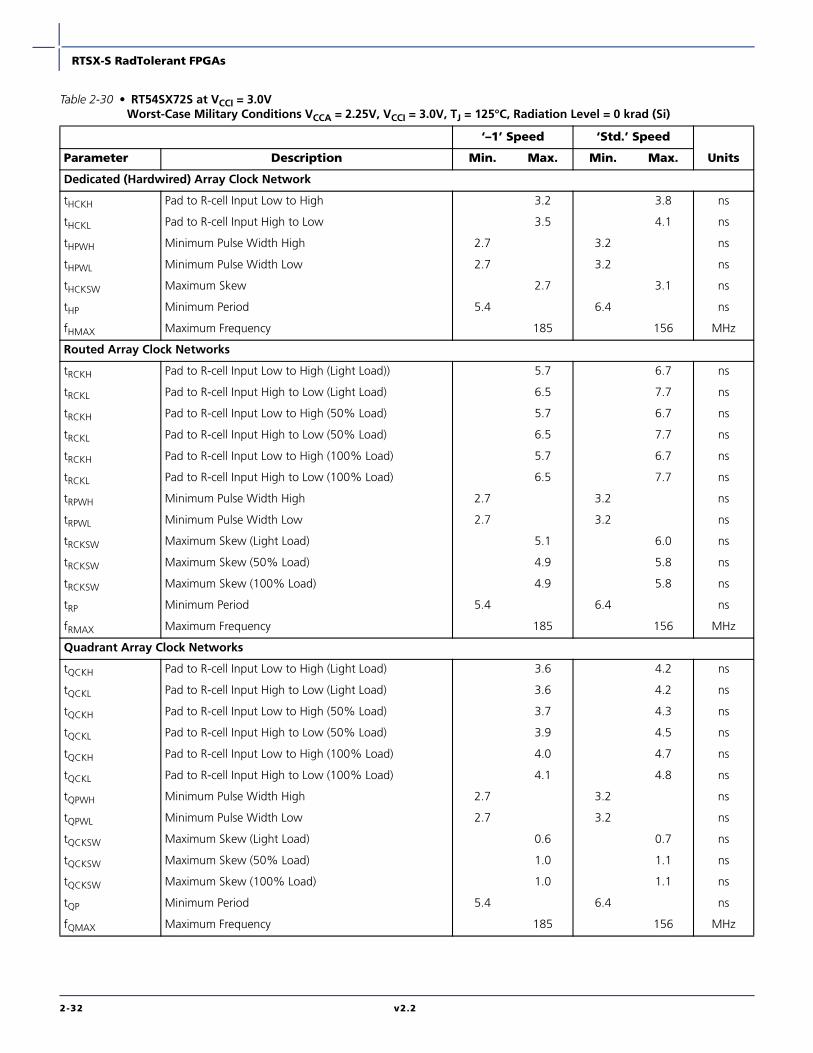
RTSX-S RadTolerant FPGAs
Table 2-30 • RT54SX72S at VCCI = 3.0VWorst-Case Military Conditions VCCA = 2.25V, VCCI = 3.0V, TJ = 125°C, Radiation Level = 0 krad (Si)
‘–1’ Speed ‘Std.’ Speed
UnitsParameter Description Min. Max. Min. Max.
Dedicated (Hardwired) Array Clock Network
tHCKH Pad to R-cell Input Low to High 3.2 3.8 ns
tHCKL Pad to R-cell Input High to Low 3.5 4.1 ns
tHPWH Minimum Pulse Width High 2.7 3.2 ns
tHPWL Minimum Pulse Width Low 2.7 3.2 ns
tHCKSW Maximum Skew 2.7 3.1 ns
tHP Minimum Period 5.4 6.4 ns
fHMAX Maximum Frequency 185 156 MHz
Routed Array Clock Networks
tRCKH Pad to R-cell Input Low to High (Light Load)) 5.7 6.7 ns
tRCKL Pad to R-cell Input High to Low (Light Load) 6.5 7.7 ns
tRCKH Pad to R-cell Input Low to High (50% Load) 5.7 6.7 ns
tRCKL Pad to R-cell Input High to Low (50% Load) 6.5 7.7 ns
tRCKH Pad to R-cell Input Low to High (100% Load) 5.7 6.7 ns
tRCKL Pad to R-cell Input High to Low (100% Load) 6.5 7.7 ns
tRPWH Minimum Pulse Width High 2.7 3.2 ns
tRPWL Minimum Pulse Width Low 2.7 3.2 ns
tRCKSW Maximum Skew (Light Load) 5.1 6.0 ns
tRCKSW Maximum Skew (50% Load) 4.9 5.8 ns
tRCKSW Maximum Skew (100% Load) 4.9 5.8 ns
tRP Minimum Period 5.4 6.4 ns
fRMAX Maximum Frequency 185 156 MHz
Quadrant Array Clock Networks
tQCKH Pad to R-cell Input Low to High (Light Load) 3.6 4.2 ns
tQCKL Pad to R-cell Input High to Low (Light Load) 3.6 4.2 ns
tQCKH Pad to R-cell Input Low to High (50% Load) 3.7 4.3 ns
tQCKL Pad to R-cell Input High to Low (50% Load) 3.9 4.5 ns
tQCKH Pad to R-cell Input Low to High (100% Load) 4.0 4.7 ns
tQCKL Pad to R-cell Input High to Low (100% Load) 4.1 4.8 ns
tQPWH Minimum Pulse Width High 2.7 3.2 ns
tQPWL Minimum Pulse Width Low 2.7 3.2 ns
tQCKSW Maximum Skew (Light Load) 0.6 0.7 ns
tQCKSW Maximum Skew (50% Load) 1.0 1.1 ns
tQCKSW Maximum Skew (100% Load) 1.0 1.1 ns
tQP Minimum Period 5.4 6.4 ns
fQMAX Maximum Frequency 185 156 MHz
2-32 v2.2
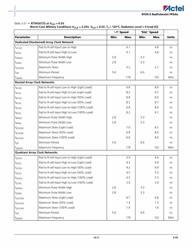
RTSX-S RadTolerant FPGAs
Table 2-31 • RT54SX72S at VCCI = 4.5VWorst-Case Military Conditions VCCA = 2.25V, VCCI = 4.5V, TJ = 125°C, Radiation Level = 0 krad (Si)
‘–1’ Speed ‘Std.’ Speed
UnitsParameter Description Min. Max. Min. Max.
Dedicated (Hardwired) Array Clock Network
tHCKH Pad to R-cell Input Low to High 4.1 4.8 ns
tHCKL Pad to R-cell Input High to Low 4.1 4.8 ns
tHPWH Minimum Pulse Width High 2.8 3.3 ns
tHPWL Minimum Pulse Width Low 2.8 3.3 ns
tHCKSW Maximum Skew 3.2 3.7 ns
tHP Minimum Period 5.6 6.6 ns
fHMAX Maximum Frequency 179 152 MHz
Routed Array Clock Networks
tRCKH Pad to R-cell Input Low to High (Light Load)) 6.8 8.0 ns
tRCKL Pad to R-cell Input High to Low (Light Load) 8.2 9.7 ns
tRCKH Pad to R-cell Input Low to High (50% Load) 6.8 8.0 ns
tRCKL Pad to R-cell Input High to Low (50% Load) 8.2 9.7 ns
tRCKH Pad to R-cell Input Low to High (100% Load) 6.8 8.0 ns
tRCKL Pad to R-cell Input High to Low (100% Load) 8.2 9.7 ns
tRPWH Minimum Pulse Width High 2.8 3.3 ns
tRPWL Minimum Pulse Width Low 2.8 3.3 ns
tRCKSW Maximum Skew (Light Load) 7.0 8.2 ns
tRCKSW Maximum Skew (50% Load) 6.8 8.0 ns
tRCKSW Maximum Skew (100% Load) 6.8 8.0 ns
tQP Minimum Period 5.6 6.6 ns
fQMAX Maximum Frequency 179 152 MHz
Quadrant Array Clock Networks
tQCKH Pad to R-cell Input Low to High (Light Load)) 3.9 4.6 ns
tQCKL Pad to R-cell Input High to Low (Light Load) 4.2 4.9 ns
tQCKH Pad to R-cell Input Low to High (50% Load) 4.2 4.9 ns
tQCKL Pad to R-cell Input High to Low (50% Load) 4.5 5.3 ns
tQCKH Pad to R-cell Input Low to High (100% Load) 4.5 5.3 ns
tQCKL Pad to R-cell Input High to Low (100% Load) 5.0 5.9 ns
tQPWH Minimum Pulse Width High 2.8 3.3 ns
tQPWL Minimum Pulse Width Low 2.8 3.3 ns
tQCKSW Maximum Skew (Light Load) 0.7 0.8 ns
tQCKSW Maximum Skew (50% Load) 1.3 1.5 ns
tQCKSW Maximum Skew (100% Load) 1.4 1.6 ns
tQP Minimum Period 5.6 6.6 ns
fQMAX Maximum Frequency 179 152 MHz
v2.2 2-33
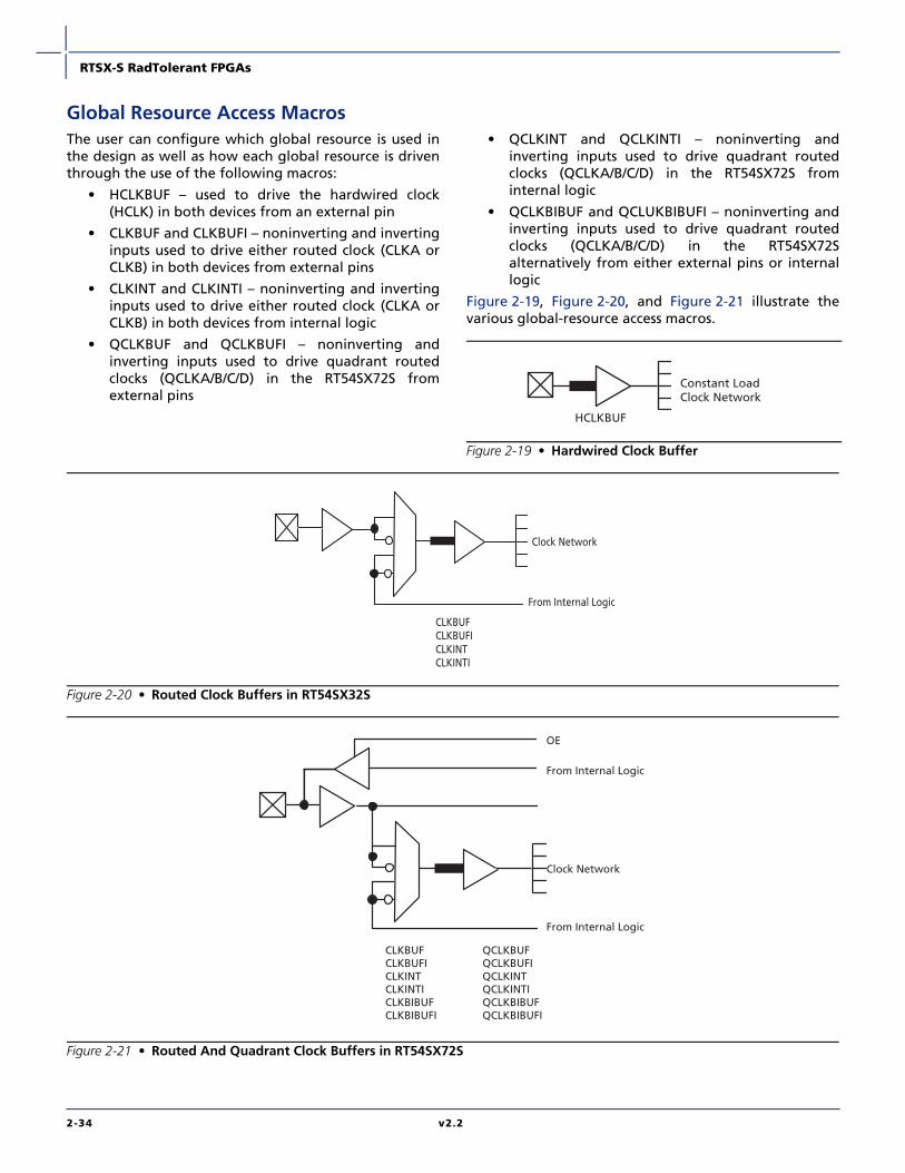
RTSX-S RadTolerant FPGAs
Global Resource Access MacrosThe user can configure which global resource is used inthe design as well as how each global resource is driventhrough the use of the following macros:
• HCLKBUF – used to drive the hardwired clock(HCLK) in both devices from an external pin
• CLKBUF and CLKBUFI – noninverting and invertinginputs used to drive either routed clock (CLKA orCLKB) in both devices from external pins
• CLKINT and CLKINTI – noninverting and invertinginputs used to drive either routed clock (CLKA orCLKB) in both devices from internal logic
• QCLKBUF and QCLKBUFI – noninverting andinverting inputs used to drive quadrant routedclocks (QCLKA/B/C/D) in the RT54SX72S fromexternal pins
• QCLKINT and QCLKINTI – noninverting andinverting inputs used to drive quadrant routedclocks (QCLKA/B/C/D) in the RT54SX72S frominternal logic
• QCLKBIBUF and QCLUKBIBUFI – noninverting andinverting inputs used to drive quadrant routedclocks (QCLKA/B/C/D) in the RT54SX72Salternatively from either external pins or internallogic
Figure 2-19, Figure 2-20, and Figure 2-21 illustrate thevarious global-resource access macros.
Figure 2-19 • Hardwired Clock Buffer
Constant Load Clock Network
HCLKBUF
Figure 2-20 • Routed Clock Buffers in RT54SX32S
Figure 2-21 • Routed And Quadrant Clock Buffers in RT54SX72S
Clock Network
From Internal Logic
CLKBUFCLKBUFICLKINTCLKINTI
Clock Network
From Internal Logic
From Internal Logic
OE
QCLKBUFQCLKBUFIQCLKINTQCLKINTIQCLKBIBUFQCLKBIBUFI
CLKBUFCLKBUFICLKINTCLKINTICLKBIBUFCLKBIBUFI
2-34 v2.2
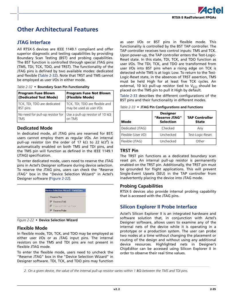
RTSX-S RadTolerant FPGAs
Other Architectural Features
JTAG InterfaceAll RTSX-S devices are IEEE 1149.1 compliant and offersuperior diagnostic and testing capabilities by providingBoundary Scan Testing (BST) and probing capabilities.The BST function is controlled through special JTAG pins(TMS, TDI, TCK, TDO, and TRST). The functionality of theJTAG pins is defined by two available modes: dedicatedand flexible (Table 2-32). Note that TRST and TMS cannotbe employed as user I/Os in either mode.
Dedicated ModeIn dedicated mode, all JTAG pins are reserved for BST;users cannot employ them as regular I/Os. An internalpull-up resistor (on the order of 17 kΩ to 22 kΩ2) isautomatically enabled on both TMS and TDI pins, andthe TMS pin will function as defined in the IEEE 1149.1(JTAG) specification.
To enter dedicated mode, users need to reserve the JTAGpins in Actel’s Designer software during device selection.To reserve the JTAG pins, users can check the "ReserveJTAG" box in the "Device Selection Wizard" in Actel’sDesigner software (Figure 2-22).
Flexible ModeIn flexible mode, TDI, TCK, and TDO may be employed aseither user I/Os or as JTAG input pins. The internalresistors on the TMS and TDI pins are not present inflexible JTAG mode.
To enter the flexible mode, users need to uncheck the"Reserve JTAG" box in the "Device Selection Wizard" inDesigner software. TDI, TCK, and TDO pins may function
as user I/Os or BST pins in flexible mode. Thisfunctionality is controlled by the BST TAP controller. TheTAP controller receives two control inputs: TMS and TCK.Upon power-up, the TAP controller enters the Test-Logic-Reset state. In this state, TDI, TCK, and TDO function asuser I/Os. The TDI, TCK, and TDO are transformed fromuser I/Os into BST pins when a rising edge on TCK isdetected while TMS is at logic Low. To return to the Test-Logic-Reset state, in the absences of TRST assertion, TMSmust be held High for at least five TCK cycles. Anexternal, 10 kΩ pull-up resistor tied to VCCI should beplaced on the TMS pin to pull it High by default.
Table 2-33 describes the different configurations of theBST pins and their functionality in different modes.
TRST PinThe TRST pin functions as a dedicated boundary scanreset pin. An internal pull-up resistor is permanentlyenabled on the TRST pin. Additionally, the TRST pin mustbe grounded for flight applications. This will preventSingle-Event Upsets (SEU) in the TAP controller frominadvertently placing the device into JTAG mode.
Probing CapabilitiesRTSX-S devices also provide internal probing capabilitythat is accessed with the JTAG pins.
Silicon Explorer II Probe InterfaceActel’s Silicon Explorer II is an integrated hardware andsoftware solution that, in conjunction with Actel’sDesigner software, allows users to examine any of theinternal nets of the device while it is operating in aprototype or a production system. The user can probetwo nodes at a time without changing the placement orrouting of the design and without using any additionaldevice resources. Highlighted nets in Designer’sChipEditor can be accessed using Silicon Explorer II inorder to observe their real time values.
Table 2-32 • Boundary Scan Pin Functionality
Program Fuse Blown (Dedicated Test Mode)
Program Fuse Not Blown (Flexible Mode)
TCK, TDI, TDO are dedicated BST pins
TCK, TDI, TDO are flexible and may be used as user I/Os
No need for pull-up resistor for TMS
Use a pull-up resistor of 10 kΩ on TMS
2. On a given device, the value of the internal pull-up resistor varies within 1 kΩ between the TMS and TDI pins.
Figure 2-22 • Device Selection Wizard
Table 2-33 • JTAG Pin Configurations and Functions
Mode
Designer "Reserve JTAG"
SelectionTAP Controller
State
Dedicated (JTAG) Checked Any
Flexible (User I/O) Unchecked Test-Logic-Reset
Flexible (JTAG) Unchecked Other
v2.2 2-35
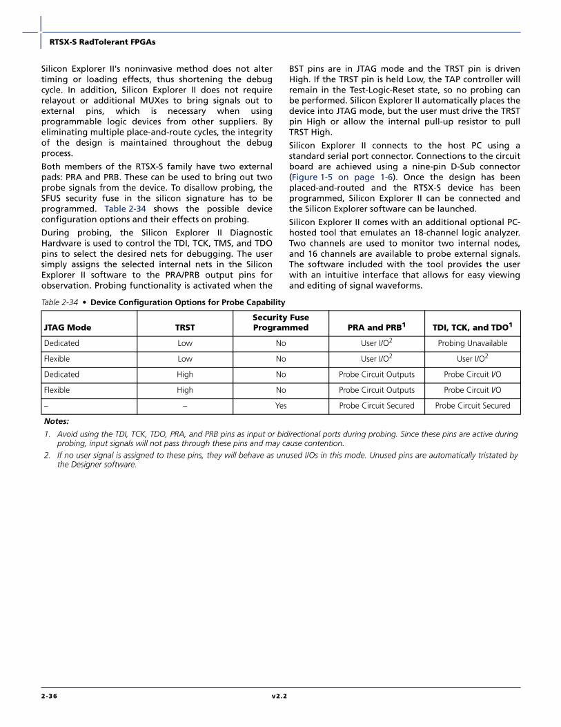
RTSX-S RadTolerant FPGAs
Silicon Explorer II's noninvasive method does not altertiming or loading effects, thus shortening the debugcycle. In addition, Silicon Explorer II does not requirerelayout or additional MUXes to bring signals out toexternal pins, which is necessary when usingprogrammable logic devices from other suppliers. Byeliminating multiple place-and-route cycles, the integrityof the design is maintained throughout the debugprocess.
Both members of the RTSX-S family have two externalpads: PRA and PRB. These can be used to bring out twoprobe signals from the device. To disallow probing, theSFUS security fuse in the silicon signature has to beprogrammed. Table 2-34 shows the possible deviceconfiguration options and their effects on probing.
During probing, the Silicon Explorer II DiagnosticHardware is used to control the TDI, TCK, TMS, and TDOpins to select the desired nets for debugging. The usersimply assigns the selected internal nets in the SiliconExplorer II software to the PRA/PRB output pins forobservation. Probing functionality is activated when the
BST pins are in JTAG mode and the TRST pin is drivenHigh. If the TRST pin is held Low, the TAP controller willremain in the Test-Logic-Reset state, so no probing canbe performed. Silicon Explorer II automatically places thedevice into JTAG mode, but the user must drive the TRSTpin High or allow the internal pull-up resistor to pullTRST High.
Silicon Explorer II connects to the host PC using astandard serial port connector. Connections to the circuitboard are achieved using a nine-pin D-Sub connector(Figure 1-5 on page 1-6). Once the design has beenplaced-and-routed and the RTSX-S device has beenprogrammed, Silicon Explorer II can be connected andthe Silicon Explorer software can be launched.
Silicon Explorer II comes with an additional optional PC-hosted tool that emulates an 18-channel logic analyzer.Two channels are used to monitor two internal nodes,and 16 channels are available to probe external signals.The software included with the tool provides the userwith an intuitive interface that allows for easy viewingand editing of signal waveforms.
Table 2-34 • Device Configuration Options for Probe Capability
JTAG Mode TRSTSecurity Fuse Programmed PRA and PRB1 TDI, TCK, and TDO1
Dedicated Low No User I/O2 Probing Unavailable
Flexible Low No User I/O2 User I/O2
Dedicated High No Probe Circuit Outputs Probe Circuit I/O
Flexible High No Probe Circuit Outputs Probe Circuit I/O
– – Yes Probe Circuit Secured Probe Circuit Secured
Notes:
1. Avoid using the TDI, TCK, TDO, PRA, and PRB pins as input or bidirectional ports during probing. Since these pins are active duringprobing, input signals will not pass through these pins and may cause contention.
2. If no user signal is assigned to these pins, they will behave as unused I/Os in this mode. Unused pins are automatically tristated bythe Designer software.
2-36 v2.2
RTSX-S RadTolerant FPGAs
Security Fuses Actel antifuse FPGAs, with FuseLock technology, offerthe highest level of design security available in aprogrammable logic device. Since antifuse FPGAs are liveat power-up, there is no bitstream that can beintercepted, and no bitstream or programming data isever downloaded to the device, thus making devicecloning impossible. In addition, special security fuses arehidden throughout the fabric of the device and may beprogrammed by the user to thwart attempts to reverseengineer the device by attempting to exploit either theprogramming or probing interfaces. Both invasive andnoninvasive attacks against an RTSX-S device that accessor bypass these security fuses will destroy access to therest of the device. Refer to the Understanding ActelAntifuse Device Security white paper for moreinformation.
Look for this symbol to ensure your valuable IP issecure(Figure 2-23).
To ensure maximum security in RTSX-S devices, it isrecommended that the user program the device securityfuse (SFUS). When programmed, the Silicon Explorer IItesting probes are disabled to prevent internal probing,and the programming interface is also disabled. All JTAGpublic instructions are still accessible by the user. Formore information, refer to Actel’s Implementation ofSecurity in Actel Antifuse FPGAs application note.
Programming Device programming is supported through the SiliconSculptor II, a single-site, robust and compact device-programmer for the PC. Two Silicon Sculptor IIs can bedaisy-chained and controlled from a single PC host. Withstandalone software for the PC, Silicon Sculptor II isdesigned to allow concurrent programming of multipleunits from the same PC when daisy-chained.
Silicon Sculptor II programs devices independently toachieve the fastest programming times possible. Eachfuse is verified by Silicon Sculptor II to ensure correctprogramming. Furthermore, at the end of programming,there are integrity tests that are run to ensure thatprogramming was completed properly. Not only does ittest programmed and nonprogrammed fuses, SiliconSculptor II also provides a self-test to extensively test itsown hardware.
Programming an RTSX-S device using Silicon Sculptor II issimilar to programming any other antifuse device. Theprocedure is as follows:
1. Load the .AFM file.
2. Select the device to be programmed.
3. Begin programming.
When the design is ready to go to production, Acteloffers volume programming services either throughdistribution partners or via our In-House ProgrammingCenter. For more details on programming the RTSX-Sdevices, please refer to the Silicon Sculptor II User’sGuide.
Figure 2-23 • FuseLock Logo
™
eu
v2.2 2-37

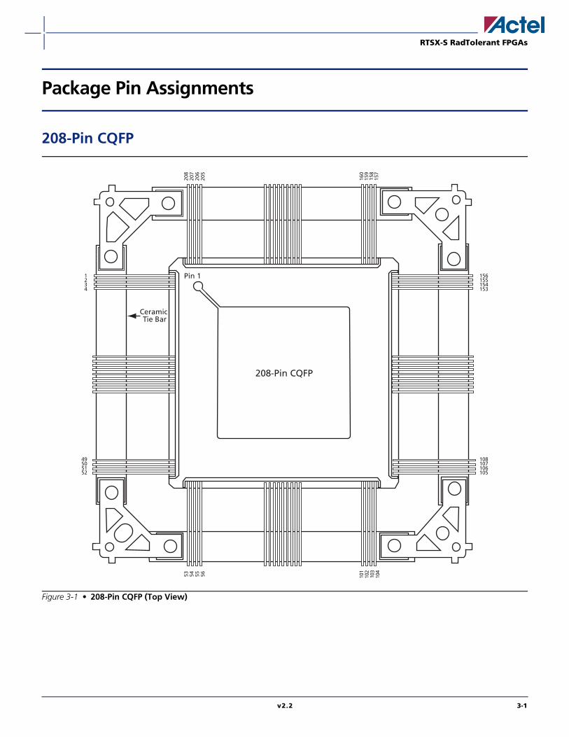
RTSX-S RadTolerant FPGAs
Package Pin Assignments
208-Pin CQFP
Figure 3-1 • 208-Pin CQFP (Top View)
CeramicTie Bar
208-Pin CQFP
1234
49505152
53 54 55 56 101
102
103
104
156155154153
108107106105
208
207
206
205
160
159
158
157
Pin 1
v2.2 3-1
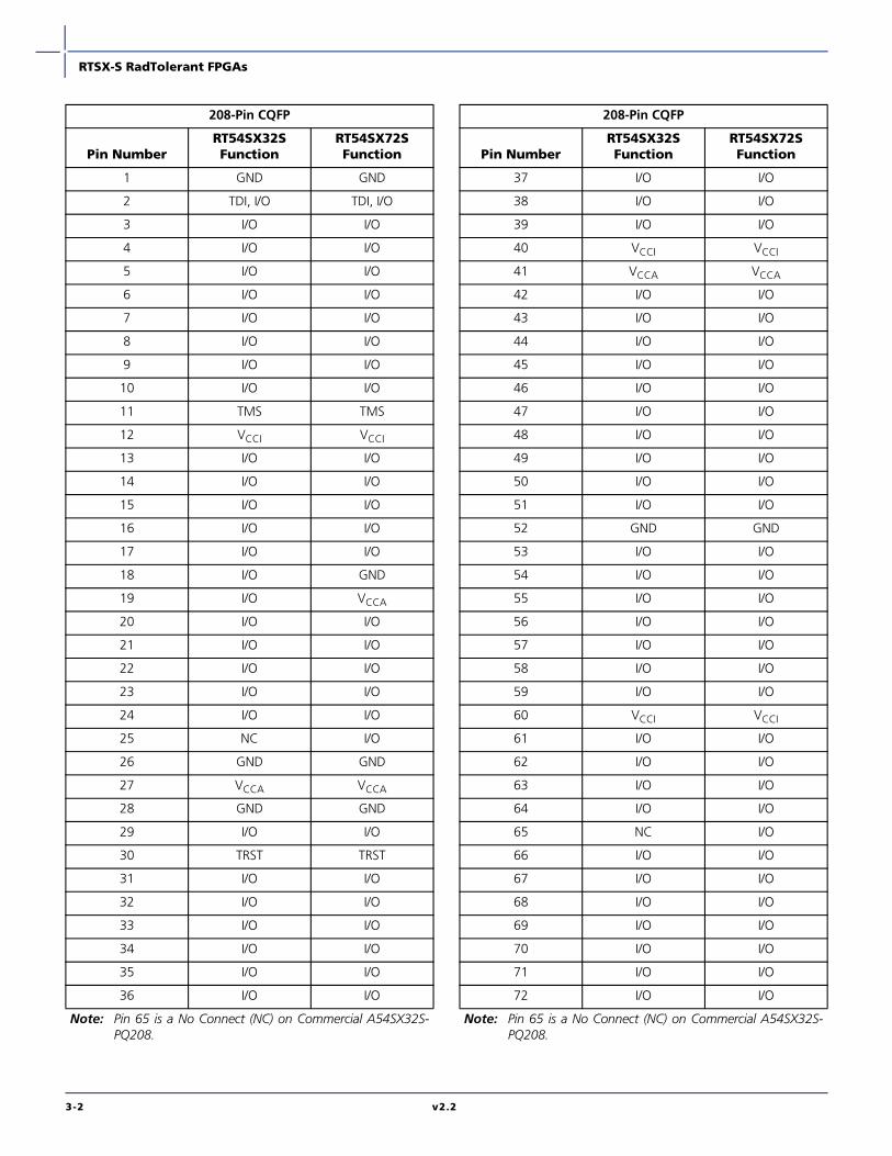
RTSX-S RadTolerant FPGAs
208-Pin CQFP
Pin NumberRT54SX32SFunction
RT54SX72SFunction
1 GND GND
2 TDI, I/O TDI, I/O
3 I/O I/O
4 I/O I/O
5 I/O I/O
6 I/O I/O
7 I/O I/O
8 I/O I/O
9 I/O I/O
10 I/O I/O
11 TMS TMS
12 VCCI VCCI
13 I/O I/O
14 I/O I/O
15 I/O I/O
16 I/O I/O
17 I/O I/O
18 I/O GND
19 I/O VCCA
20 I/O I/O
21 I/O I/O
22 I/O I/O
23 I/O I/O
24 I/O I/O
25 NC I/O
26 GND GND
27 VCCA VCCA
28 GND GND
29 I/O I/O
30 TRST TRST
31 I/O I/O
32 I/O I/O
33 I/O I/O
34 I/O I/O
35 I/O I/O
36 I/O I/O
Note: Pin 65 is a No Connect (NC) on Commercial A54SX32S-PQ208.
37 I/O I/O
38 I/O I/O
39 I/O I/O
40 VCCI VCCI
41 VCCA VCCA
42 I/O I/O
43 I/O I/O
44 I/O I/O
45 I/O I/O
46 I/O I/O
47 I/O I/O
48 I/O I/O
49 I/O I/O
50 I/O I/O
51 I/O I/O
52 GND GND
53 I/O I/O
54 I/O I/O
55 I/O I/O
56 I/O I/O
57 I/O I/O
58 I/O I/O
59 I/O I/O
60 VCCI VCCI
61 I/O I/O
62 I/O I/O
63 I/O I/O
64 I/O I/O
65 NC I/O
66 I/O I/O
67 I/O I/O
68 I/O I/O
69 I/O I/O
70 I/O I/O
71 I/O I/O
72 I/O I/O
208-Pin CQFP
Pin NumberRT54SX32SFunction
RT54SX72SFunction
Note: Pin 65 is a No Connect (NC) on Commercial A54SX32S-PQ208.
3-2 v2.2

RTSX-S RadTolerant FPGAs
73 I/O I/O
74 I/O QCLKA, I/O
75 I/O I/O
76 PRB, I/O PRB, I/O
77 GND GND
78 VCCA VCCA
79 GND GND
80 NC NC
81 I/O I/O
82 HCLK HCLK
83 I/O VCCI
84 I/O QCLKB, I/O
85 I/O I/O
86 I/O I/O
87 I/O I/O
88 I/O I/O
89 I/O I/O
90 I/O I/O
91 I/O I/O
92 I/O I/O
93 I/O I/O
94 I/O I/O
95 I/O I/O
96 I/O I/O
97 I/O I/O
98 VCCI VCCI
99 I/O I/O
100 I/O I/O
101 I/O I/O
102 I/O I/O
103 TDO, I/O TDO, I/O
104 I/O I/O
105 GND GND
106 I/O I/O
107 I/O I/O
108 I/O I/O
208-Pin CQFP
Pin NumberRT54SX32SFunction
RT54SX72SFunction
Note: Pin 65 is a No Connect (NC) on Commercial A54SX32S-PQ208.
109 I/O I/O
110 I/O I/O
111 I/O I/O
112 I/O I/O
113 I/O I/O
114 VCCA VCCA
115 VCCI VCCI
116 I/O GND
117 I/O VCCA
118 I/O I/O
119 I/O I/O
120 I/O I/O
121 I/O I/O
122 I/O I/O
123 I/O I/O
124 I/O I/O
125 I/O I/O
126 I/O I/O
127 I/O I/O
128 I/O I/O
129 GND GND
130 VCCA VCCA
131 GND GND
132 NC I/O
133 I/O I/O
134 I/O I/O
135 I/O I/O
136 I/O I/O
137 I/O I/O
138 I/O I/O
139 I/O I/O
140 I/O I/O
141 I/O I/O
142 I/O I/O
143 I/O I/O
144 I/O I/O
208-Pin CQFP
Pin NumberRT54SX32SFunction
RT54SX72SFunction
Note: Pin 65 is a No Connect (NC) on Commercial A54SX32S-PQ208.
v2.2 3-3
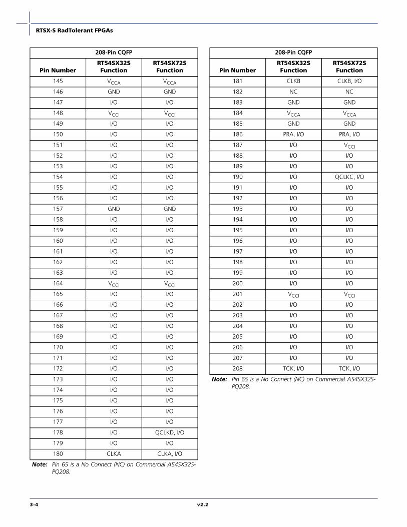
RTSX-S RadTolerant FPGAs
145 VCCA VCCA
146 GND GND
147 I/O I/O
148 VCCI VCCI
149 I/O I/O
150 I/O I/O
151 I/O I/O
152 I/O I/O
153 I/O I/O
154 I/O I/O
155 I/O I/O
156 I/O I/O
157 GND GND
158 I/O I/O
159 I/O I/O
160 I/O I/O
161 I/O I/O
162 I/O I/O
163 I/O I/O
164 VCCI VCCI
165 I/O I/O
166 I/O I/O
167 I/O I/O
168 I/O I/O
169 I/O I/O
170 I/O I/O
171 I/O I/O
172 I/O I/O
173 I/O I/O
174 I/O I/O
175 I/O I/O
176 I/O I/O
177 I/O I/O
178 I/O QCLKD, I/O
179 I/O I/O
180 CLKA CLKA, I/O
208-Pin CQFP
Pin NumberRT54SX32SFunction
RT54SX72SFunction
Note: Pin 65 is a No Connect (NC) on Commercial A54SX32S-PQ208.
181 CLKB CLKB, I/O
182 NC NC
183 GND GND
184 VCCA VCCA
185 GND GND
186 PRA, I/O PRA, I/O
187 I/O VCCI
188 I/O I/O
189 I/O I/O
190 I/O QCLKC, I/O
191 I/O I/O
192 I/O I/O
193 I/O I/O
194 I/O I/O
195 I/O I/O
196 I/O I/O
197 I/O I/O
198 I/O I/O
199 I/O I/O
200 I/O I/O
201 VCCI VCCI
202 I/O I/O
203 I/O I/O
204 I/O I/O
205 I/O I/O
206 I/O I/O
207 I/O I/O
208 TCK, I/O TCK, I/O
208-Pin CQFP
Pin NumberRT54SX32SFunction
RT54SX72SFunction
Note: Pin 65 is a No Connect (NC) on Commercial A54SX32S-PQ208.
3-4 v2.2
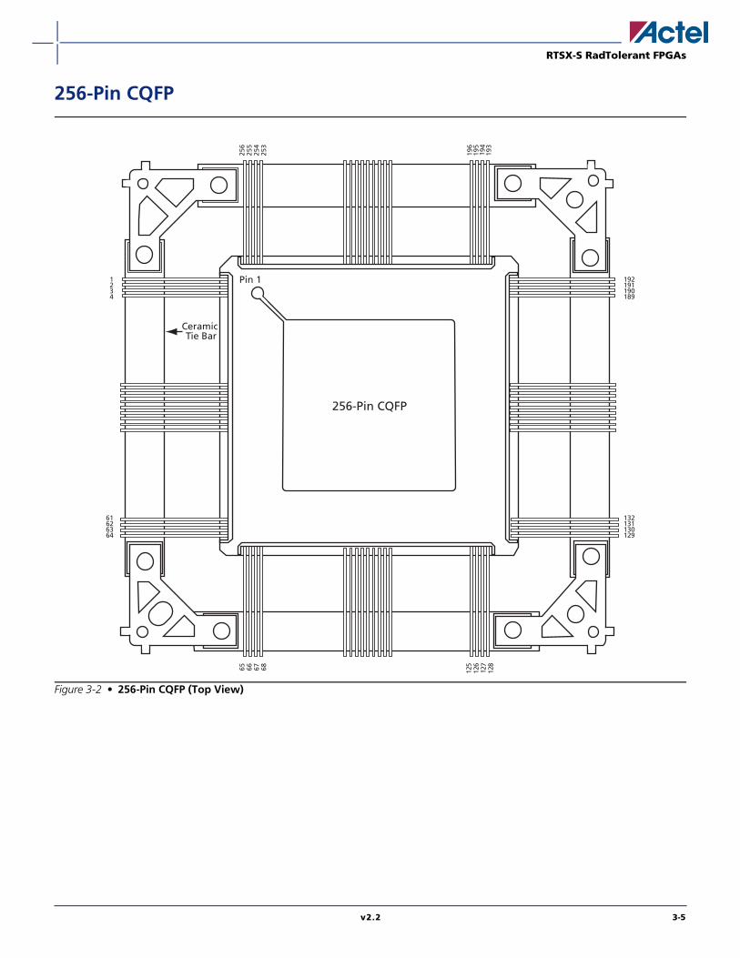
RTSX-S RadTolerant FPGAs
256-Pin CQFP
Figure 3-2 • 256-Pin CQFP (Top View)
CeramicTie Bar
256-Pin CQFP
1234
61626364
65 66 67 68 125
126
127
128
192191190189
132131130129
256
255
254
253
196
195
194
193
Pin 1
v2.2 3-5
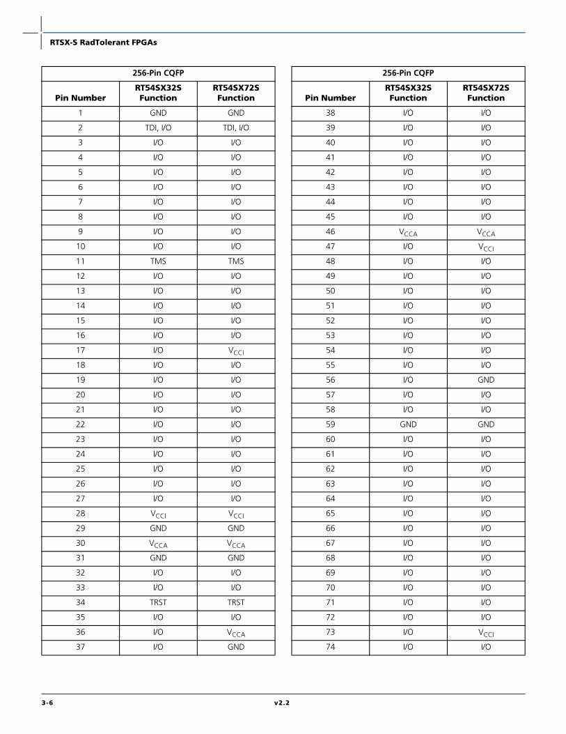
RTSX-S RadTolerant FPGAs
256-Pin CQFP
Pin NumberRT54SX32SFunction
RT54SX72SFunction
1 GND GND
2 TDI, I/O TDI, I/O
3 I/O I/O
4 I/O I/O
5 I/O I/O
6 I/O I/O
7 I/O I/O
8 I/O I/O
9 I/O I/O
10 I/O I/O
11 TMS TMS
12 I/O I/O
13 I/O I/O
14 I/O I/O
15 I/O I/O
16 I/O I/O
17 I/O VCCI
18 I/O I/O
19 I/O I/O
20 I/O I/O
21 I/O I/O
22 I/O I/O
23 I/O I/O
24 I/O I/O
25 I/O I/O
26 I/O I/O
27 I/O I/O
28 VCCI VCCI
29 GND GND
30 VCCA VCCA
31 GND GND
32 I/O I/O
33 I/O I/O
34 TRST TRST
35 I/O I/O
36 I/O VCCA
37 I/O GND
38 I/O I/O
39 I/O I/O
40 I/O I/O
41 I/O I/O
42 I/O I/O
43 I/O I/O
44 I/O I/O
45 I/O I/O
46 VCCA VCCA
47 I/O VCCI
48 I/O I/O
49 I/O I/O
50 I/O I/O
51 I/O I/O
52 I/O I/O
53 I/O I/O
54 I/O I/O
55 I/O I/O
56 I/O GND
57 I/O I/O
58 I/O I/O
59 GND GND
60 I/O I/O
61 I/O I/O
62 I/O I/O
63 I/O I/O
64 I/O I/O
65 I/O I/O
66 I/O I/O
67 I/O I/O
68 I/O I/O
69 I/O I/O
70 I/O I/O
71 I/O I/O
72 I/O I/O
73 I/O VCCI
74 I/O I/O
256-Pin CQFP
Pin NumberRT54SX32SFunction
RT54SX72SFunction
3-6 v2.2
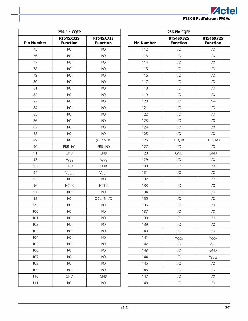
RTSX-S RadTolerant FPGAs
75 I/O I/O
76 I/O I/O
77 I/O I/O
78 I/O I/O
79 I/O I/O
80 I/O I/O
81 I/O I/O
82 I/O I/O
83 I/O I/O
84 I/O I/O
85 I/O I/O
86 I/O I/O
87 I/O I/O
88 I/O I/O
89 I/O QCLKA, I/O
90 PRB, I/O PRB, I/O
91 GND GND
92 VCCI VCCI
93 GND GND
94 VCCA VCCA
95 I/O I/O
96 HCLK HCLK
97 I/O I/O
98 I/O QCLKB, I/O
99 I/O I/O
100 I/O I/O
101 I/O I/O
102 I/O I/O
103 I/O I/O
104 I/O I/O
105 I/O I/O
106 I/O I/O
107 I/O I/O
108 I/O I/O
109 I/O I/O
110 GND GND
111 I/O I/O
256-Pin CQFP
Pin NumberRT54SX32SFunction
RT54SX72SFunction
112 I/O I/O
113 I/O I/O
114 I/O I/O
115 I/O I/O
116 I/O I/O
117 I/O I/O
118 I/O I/O
119 I/O I/O
120 I/O VCCI
121 I/O I/O
122 I/O I/O
123 I/O I/O
124 I/O I/O
125 I/O I/O
126 TDO, I/O TDO, I/O
127 I/O I/O
128 GND GND
129 I/O I/O
130 I/O I/O
131 I/O I/O
132 I/O I/O
133 I/O I/O
134 I/O I/O
135 I/O I/O
136 I/O I/O
137 I/O I/O
138 I/O I/O
139 I/O I/O
140 I/O I/O
141 VCCA VCCA
142 I/O VCCI
143 I/O GND
144 I/O VCCA
145 I/O I/O
146 I/O I/O
147 I/O I/O
148 I/O I/O
256-Pin CQFP
Pin NumberRT54SX32SFunction
RT54SX72SFunction
v2.2 3-7
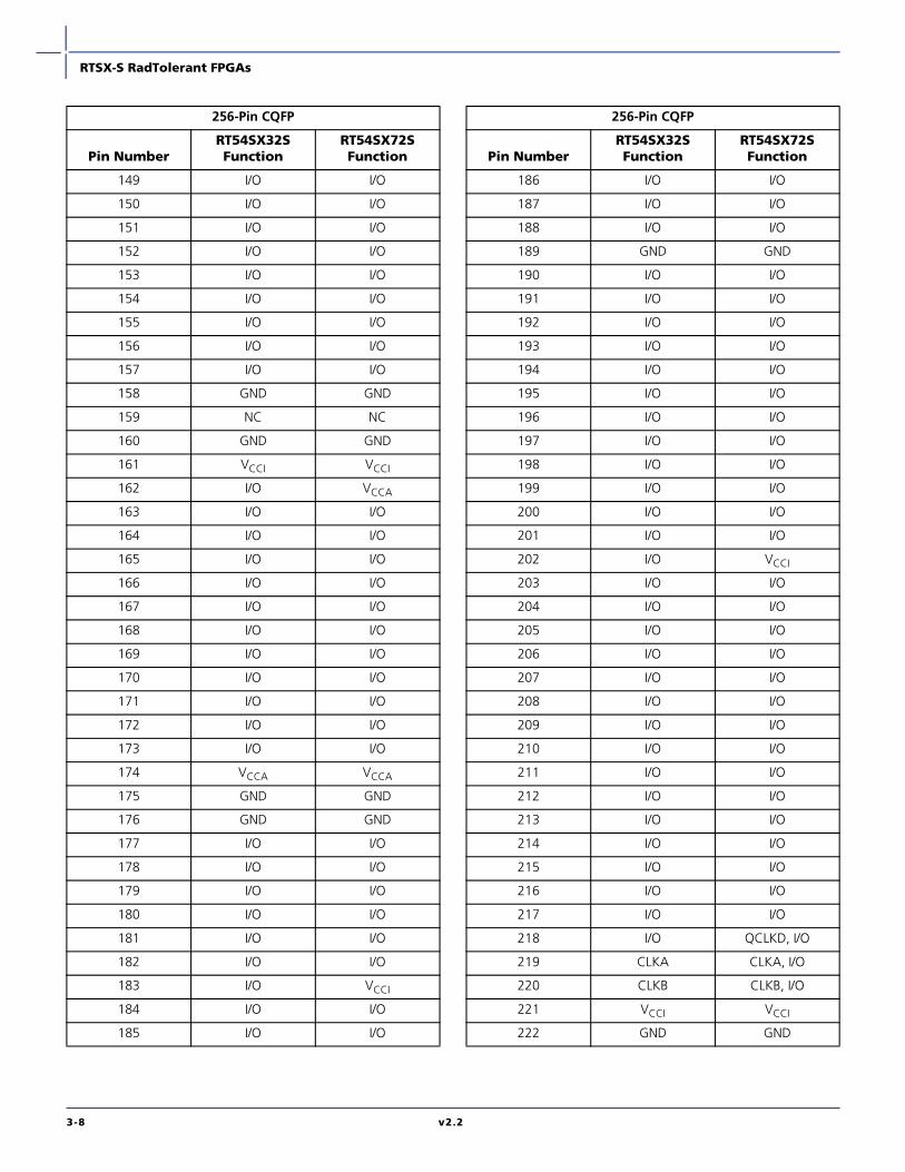
RTSX-S RadTolerant FPGAs
149 I/O I/O
150 I/O I/O
151 I/O I/O
152 I/O I/O
153 I/O I/O
154 I/O I/O
155 I/O I/O
156 I/O I/O
157 I/O I/O
158 GND GND
159 NC NC
160 GND GND
161 VCCI VCCI
162 I/O VCCA
163 I/O I/O
164 I/O I/O
165 I/O I/O
166 I/O I/O
167 I/O I/O
168 I/O I/O
169 I/O I/O
170 I/O I/O
171 I/O I/O
172 I/O I/O
173 I/O I/O
174 VCCA VCCA
175 GND GND
176 GND GND
177 I/O I/O
178 I/O I/O
179 I/O I/O
180 I/O I/O
181 I/O I/O
182 I/O I/O
183 I/O VCCI
184 I/O I/O
185 I/O I/O
256-Pin CQFP
Pin NumberRT54SX32SFunction
RT54SX72SFunction
186 I/O I/O
187 I/O I/O
188 I/O I/O
189 GND GND
190 I/O I/O
191 I/O I/O
192 I/O I/O
193 I/O I/O
194 I/O I/O
195 I/O I/O
196 I/O I/O
197 I/O I/O
198 I/O I/O
199 I/O I/O
200 I/O I/O
201 I/O I/O
202 I/O VCCI
203 I/O I/O
204 I/O I/O
205 I/O I/O
206 I/O I/O
207 I/O I/O
208 I/O I/O
209 I/O I/O
210 I/O I/O
211 I/O I/O
212 I/O I/O
213 I/O I/O
214 I/O I/O
215 I/O I/O
216 I/O I/O
217 I/O I/O
218 I/O QCLKD, I/O
219 CLKA CLKA, I/O
220 CLKB CLKB, I/O
221 VCCI VCCI
222 GND GND
256-Pin CQFP
Pin NumberRT54SX32SFunction
RT54SX72SFunction
3-8 v2.2
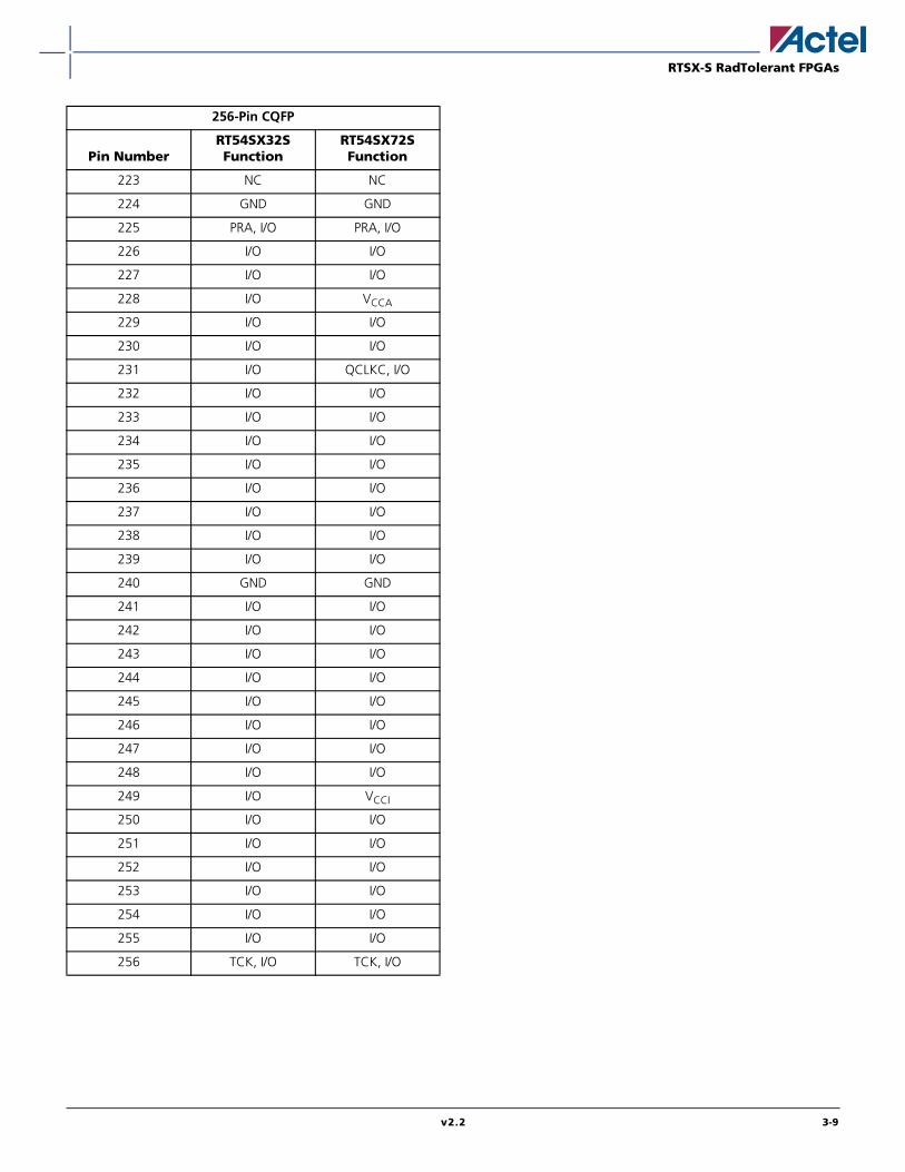
RTSX-S RadTolerant FPGAs
223 NC NC
224 GND GND
225 PRA, I/O PRA, I/O
226 I/O I/O
227 I/O I/O
228 I/O VCCA
229 I/O I/O
230 I/O I/O
231 I/O QCLKC, I/O
232 I/O I/O
233 I/O I/O
234 I/O I/O
235 I/O I/O
236 I/O I/O
237 I/O I/O
238 I/O I/O
239 I/O I/O
240 GND GND
241 I/O I/O
242 I/O I/O
243 I/O I/O
244 I/O I/O
245 I/O I/O
246 I/O I/O
247 I/O I/O
248 I/O I/O
249 I/O VCCI
250 I/O I/O
251 I/O I/O
252 I/O I/O
253 I/O I/O
254 I/O I/O
255 I/O I/O
256 TCK, I/O TCK, I/O
256-Pin CQFP
Pin NumberRT54SX32SFunction
RT54SX72SFunction
v2.2 3-9
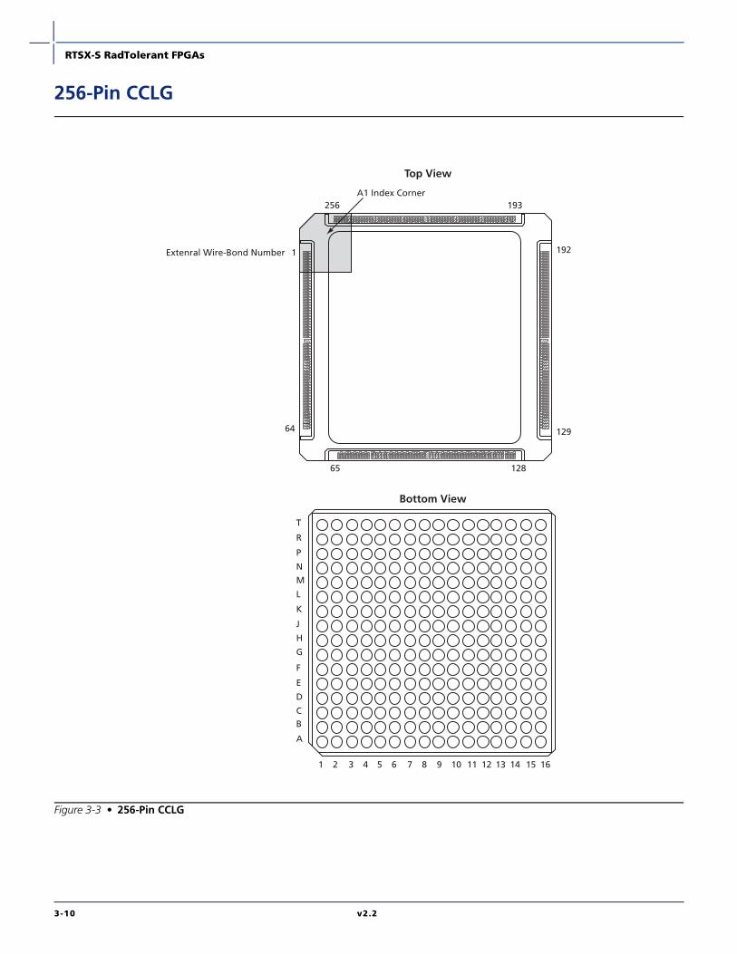
RTSX-S RadTolerant FPGAs
256-Pin CCLG
Figure 3-3 • 256-Pin CCLG
1
64
65 128
129
192
193256A1 Index Corner
Extenral Wire-Bond Number
Bottom View
Top View
A
BC
D
E
F
G
H
J
K
L
M
N
P
R
T
1 2 3 4 5 6 7 8 9 10 11 12 13 14 15 16
3-10 v2.2

RTSX-S RadTolerant FPGAs
256-Pin CCLG*
Pin NumberExternal Wire-Bond Number
RT54SX32S Function
A1 1 GND
A2 256 TCK, I/O
A3 255 I/O
A4 251 I/O
A5 243 I/O
A6 238 I/O
A7 232 I/O
A8 228 I/O
A9 227 CLKB
A10 221 I/O
A11 216 I/O
A12 209 I/O
A13 203 I/O
A14 200 I/O
A15 2 GND
A16 13 GND
B1 242 I/O
B2 22 GND
B3 254 I/O
B4 253 I/O
B5 248 I/O
B6 241 I/O
B7 234 I/O
B8 33 VCCA
B9 222 I/O
B10 220 I/O
B11 212 I/O
B12 207 I/O
B13 202 I/O
B14 198 I/O
B15 32 GND
B16 196 I/O
C1 6 I/O
C2 4 TDI,I/O
Note: *This table was sorted by the pin number.
C3 65 GND
C4 252 I/O
C5 249 I/O
C6 245 I/O
C7 239 I/O
C8 230 I/O
C9 226 CLKA
C10 218 I/O
C11 210 I/O
C12 201 I/O
C13 197 I/O
C14 211 I/O
C15 178 I/O
C16 195 I/O
D1 12 I/O
D2 8 I/O
D3 10 I/O
D4 7 I/O
D5 250 I/O
D6 244 I/O
D7 237 I/O
D8 229 PRA, I/O
D9 217 I/O
D10 208 I/O
D11 206 I/O
D12 199 I/O
D13 205 I/O
D14 173 I/O
D15 190 I/O
D16 188 I/O
E1 16 I/O
E2 15 I/O
E3 9 I/O
E4 11 I/O
256-Pin CCLG*
Pin NumberExternal Wire-Bond Number
RT54SX32S Function
Note: *This table was sorted by the pin number.
v2.2 3-11
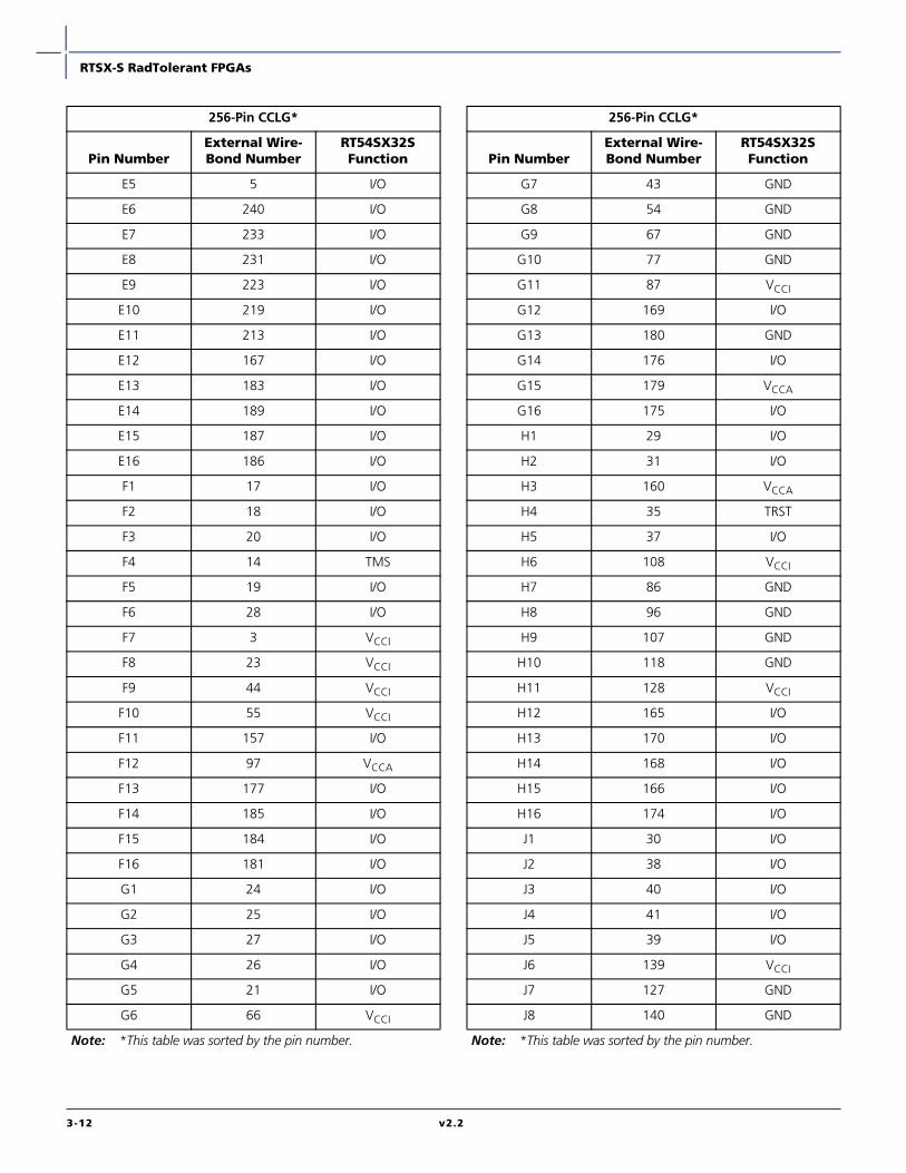
RTSX-S RadTolerant FPGAs
E5 5 I/O
E6 240 I/O
E7 233 I/O
E8 231 I/O
E9 223 I/O
E10 219 I/O
E11 213 I/O
E12 167 I/O
E13 183 I/O
E14 189 I/O
E15 187 I/O
E16 186 I/O
F1 17 I/O
F2 18 I/O
F3 20 I/O
F4 14 TMS
F5 19 I/O
F6 28 I/O
F7 3 VCCI
F8 23 VCCI
F9 44 VCCI
F10 55 VCCI
F11 157 I/O
F12 97 VCCA
F13 177 I/O
F14 185 I/O
F15 184 I/O
F16 181 I/O
G1 24 I/O
G2 25 I/O
G3 27 I/O
G4 26 I/O
G5 21 I/O
G6 66 VCCI
256-Pin CCLG*
Pin NumberExternal Wire-Bond Number
RT54SX32S Function
Note: *This table was sorted by the pin number.
G7 43 GND
G8 54 GND
G9 67 GND
G10 77 GND
G11 87 VCCI
G12 169 I/O
G13 180 GND
G14 176 I/O
G15 179 VCCA
G16 175 I/O
H1 29 I/O
H2 31 I/O
H3 160 VCCA
H4 35 TRST
H5 37 I/O
H6 108 VCCI
H7 86 GND
H8 96 GND
H9 107 GND
H10 118 GND
H11 128 VCCI
H12 165 I/O
H13 170 I/O
H14 168 I/O
H15 166 I/O
H16 174 I/O
J1 30 I/O
J2 38 I/O
J3 40 I/O
J4 41 I/O
J5 39 I/O
J6 139 VCCI
J7 127 GND
J8 140 GND
256-Pin CCLG*
Pin NumberExternal Wire-Bond Number
RT54SX32S Function
Note: *This table was sorted by the pin number.
3-12 v2.2
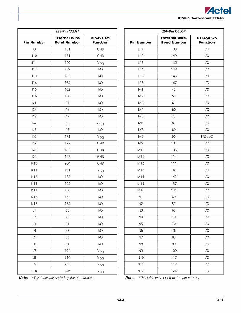
RTSX-S RadTolerant FPGAs
J9 151 GND
J10 161 GND
J11 150 VCCI
J12 159 I/O
J13 163 I/O
J14 164 I/O
J15 162 I/O
J16 158 I/O
K1 34 I/O
K2 45 I/O
K3 47 I/O
K4 50 VCCA
K5 48 I/O
K6 171 VCCI
K7 172 GND
K8 182 GND
K9 192 GND
K10 204 GND
K11 191 VCCI
K12 153 I/O
K13 155 I/O
K14 156 I/O
K15 152 I/O
K16 154 I/O
L1 36 I/O
L2 46 I/O
L3 51 I/O
L4 58 I/O
L5 52 I/O
L6 91 I/O
L7 194 VCCI
L8 214 VCCI
L9 235 VCCI
L10 246 VCCI
256-Pin CCLG*
Pin NumberExternal Wire-Bond Number
RT54SX32S Function
Note: *This table was sorted by the pin number.
L11 103 I/O
L12 149 I/O
L13 146 I/O
L14 148 I/O
L15 145 I/O
L16 147 I/O
M1 42 I/O
M2 53 I/O
M3 61 I/O
M4 60 I/O
M5 72 I/O
M6 81 I/O
M7 89 I/O
M8 95 PRB, I/O
M9 101 I/O
M10 105 I/O
M11 114 I/O
M12 111 I/O
M13 141 I/O
M14 142 I/O
M15 137 I/O
M16 144 I/O
N1 49 I/O
N2 57 I/O
N3 63 I/O
N4 79 I/O
N5 70 I/O
N6 76 I/O
N7 83 I/O
N8 99 I/O
N9 109 I/O
N10 117 I/O
N11 112 I/O
N12 124 I/O
256-Pin CCLG*
Pin NumberExternal Wire-Bond Number
RT54SX32S Function
Note: *This table was sorted by the pin number.
v2.2 3-13
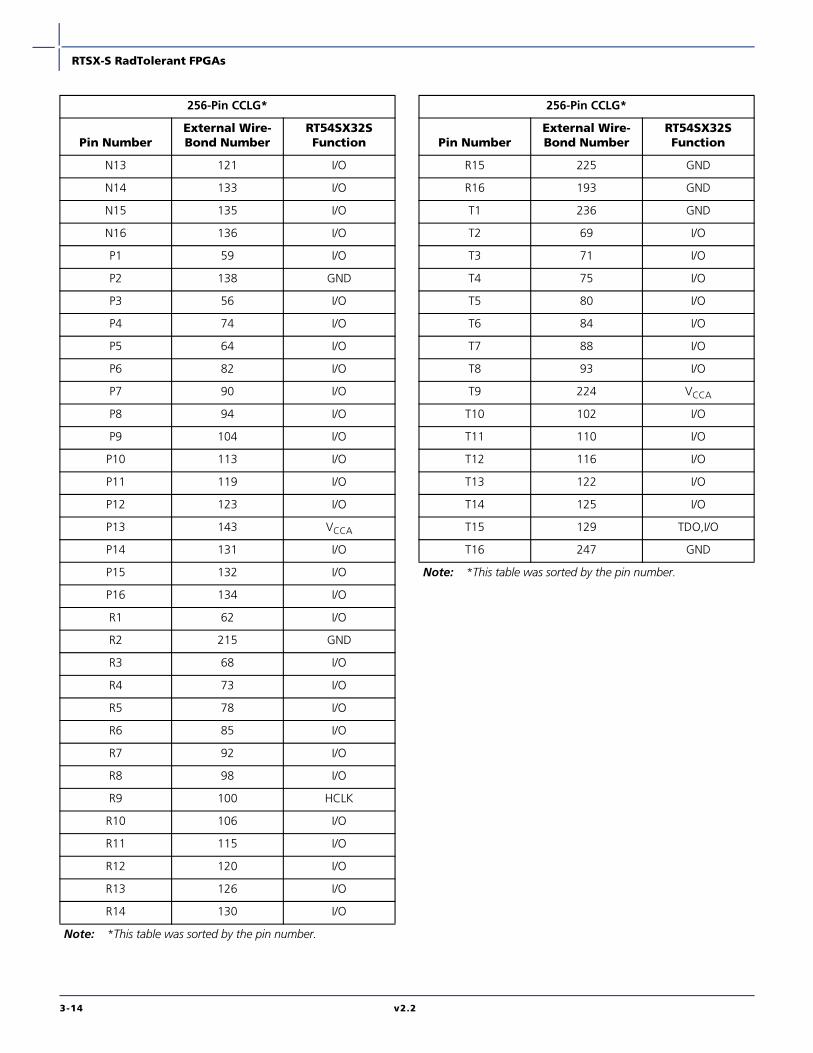
RTSX-S RadTolerant FPGAs
N13 121 I/O
N14 133 I/O
N15 135 I/O
N16 136 I/O
P1 59 I/O
P2 138 GND
P3 56 I/O
P4 74 I/O
P5 64 I/O
P6 82 I/O
P7 90 I/O
P8 94 I/O
P9 104 I/O
P10 113 I/O
P11 119 I/O
P12 123 I/O
P13 143 VCCA
P14 131 I/O
P15 132 I/O
P16 134 I/O
R1 62 I/O
R2 215 GND
R3 68 I/O
R4 73 I/O
R5 78 I/O
R6 85 I/O
R7 92 I/O
R8 98 I/O
R9 100 HCLK
R10 106 I/O
R11 115 I/O
R12 120 I/O
R13 126 I/O
R14 130 I/O
256-Pin CCLG*
Pin NumberExternal Wire-Bond Number
RT54SX32S Function
Note: *This table was sorted by the pin number.
R15 225 GND
R16 193 GND
T1 236 GND
T2 69 I/O
T3 71 I/O
T4 75 I/O
T5 80 I/O
T6 84 I/O
T7 88 I/O
T8 93 I/O
T9 224 VCCA
T10 102 I/O
T11 110 I/O
T12 116 I/O
T13 122 I/O
T14 125 I/O
T15 129 TDO,I/O
T16 247 GND
256-Pin CCLG*
Pin NumberExternal Wire-Bond Number
RT54SX32S Function
Note: *This table was sorted by the pin number.
3-14 v2.2

RTSX-S RadTolerant FPGAs
256-Pin CCLG*
Pin NumberExternal Wire-Bond Number
RT54SX32S Function
A1 1 GND
A15 2 GND
F7 3 VCCI
C2 4 TDI,I/O
E5 5 I/O
C1 6 I/O
D4 7 I/O
D2 8 I/O
E3 9 I/O
D3 10 I/O
E4 11 I/O
D1 12 I/O
A16 13 GND
F4 14 TMS
E2 15 I/O
E1 16 I/O
F1 17 I/O
F2 18 I/O
F5 19 I/O
F3 20 I/O
G5 21 I/O
B2 22 GND
F8 23 VCCI
G1 24 I/O
G2 25 I/O
G4 26 I/O
G3 27 I/O
F6 28 I/O
H1 29 I/O
J1 30 I/O
H2 31 I/O
B15 32 GND
B8 33 VCCA
K1 34 I/O
Note: *This table was sorted by the wire-bond number.
H4 35 TRST
L1 36 I/O
H5 37 I/O
J2 38 I/O
J5 39 I/O
J3 40 I/O
J4 41 I/O
M1 42 I/O
G7 43 GND
F9 44 VCCI
K2 45 I/O
L2 46 I/O
K3 47 I/O
K5 48 I/O
N1 49 I/O
K4 50 VCCA
L3 51 I/O
L5 52 I/O
M2 53 I/O
G8 54 GND
F10 55 VCCI
P3 56 I/O
N2 57 I/O
L4 58 I/O
P1 59 I/O
M4 60 I/O
M3 61 I/O
R1 62 I/O
N3 63 I/O
P5 64 I/O
C3 65 GND
G6 66 VCCI
G9 67 GND
R3 68 I/O
256-Pin CCLG*
Pin NumberExternal Wire-Bond Number
RT54SX32S Function
Note: *This table was sorted by the wire-bond number.
v2.2 3-15
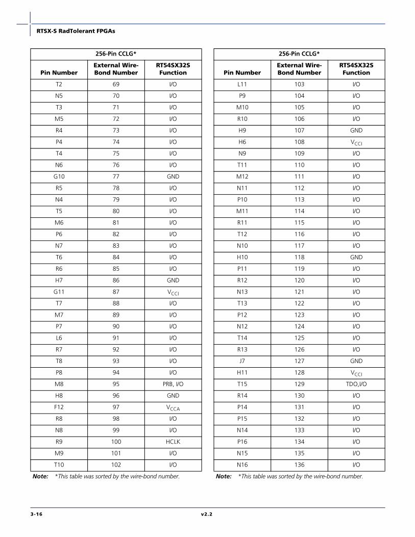
RTSX-S RadTolerant FPGAs
T2 69 I/O
N5 70 I/O
T3 71 I/O
M5 72 I/O
R4 73 I/O
P4 74 I/O
T4 75 I/O
N6 76 I/O
G10 77 GND
R5 78 I/O
N4 79 I/O
T5 80 I/O
M6 81 I/O
P6 82 I/O
N7 83 I/O
T6 84 I/O
R6 85 I/O
H7 86 GND
G11 87 VCCI
T7 88 I/O
M7 89 I/O
P7 90 I/O
L6 91 I/O
R7 92 I/O
T8 93 I/O
P8 94 I/O
M8 95 PRB, I/O
H8 96 GND
F12 97 VCCA
R8 98 I/O
N8 99 I/O
R9 100 HCLK
M9 101 I/O
T10 102 I/O
256-Pin CCLG*
Pin NumberExternal Wire-Bond Number
RT54SX32S Function
Note: *This table was sorted by the wire-bond number.
L11 103 I/O
P9 104 I/O
M10 105 I/O
R10 106 I/O
H9 107 GND
H6 108 VCCI
N9 109 I/O
T11 110 I/O
M12 111 I/O
N11 112 I/O
P10 113 I/O
M11 114 I/O
R11 115 I/O
T12 116 I/O
N10 117 I/O
H10 118 GND
P11 119 I/O
R12 120 I/O
N13 121 I/O
T13 122 I/O
P12 123 I/O
N12 124 I/O
T14 125 I/O
R13 126 I/O
J7 127 GND
H11 128 VCCI
T15 129 TDO,I/O
R14 130 I/O
P14 131 I/O
P15 132 I/O
N14 133 I/O
P16 134 I/O
N15 135 I/O
N16 136 I/O
256-Pin CCLG*
Pin NumberExternal Wire-Bond Number
RT54SX32S Function
Note: *This table was sorted by the wire-bond number.
3-16 v2.2
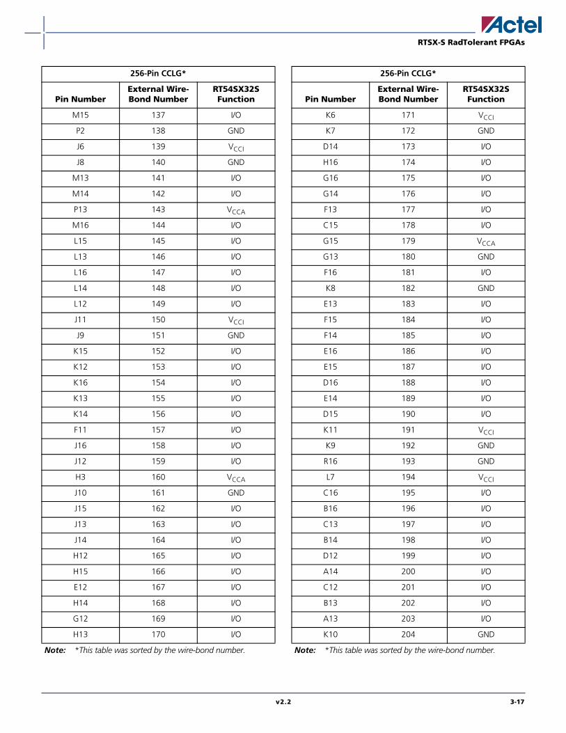
RTSX-S RadTolerant FPGAs
M15 137 I/O
P2 138 GND
J6 139 VCCI
J8 140 GND
M13 141 I/O
M14 142 I/O
P13 143 VCCA
M16 144 I/O
L15 145 I/O
L13 146 I/O
L16 147 I/O
L14 148 I/O
L12 149 I/O
J11 150 VCCI
J9 151 GND
K15 152 I/O
K12 153 I/O
K16 154 I/O
K13 155 I/O
K14 156 I/O
F11 157 I/O
J16 158 I/O
J12 159 I/O
H3 160 VCCA
J10 161 GND
J15 162 I/O
J13 163 I/O
J14 164 I/O
H12 165 I/O
H15 166 I/O
E12 167 I/O
H14 168 I/O
G12 169 I/O
H13 170 I/O
256-Pin CCLG*
Pin NumberExternal Wire-Bond Number
RT54SX32S Function
Note: *This table was sorted by the wire-bond number.
K6 171 VCCI
K7 172 GND
D14 173 I/O
H16 174 I/O
G16 175 I/O
G14 176 I/O
F13 177 I/O
C15 178 I/O
G15 179 VCCA
G13 180 GND
F16 181 I/O
K8 182 GND
E13 183 I/O
F15 184 I/O
F14 185 I/O
E16 186 I/O
E15 187 I/O
D16 188 I/O
E14 189 I/O
D15 190 I/O
K11 191 VCCI
K9 192 GND
R16 193 GND
L7 194 VCCI
C16 195 I/O
B16 196 I/O
C13 197 I/O
B14 198 I/O
D12 199 I/O
A14 200 I/O
C12 201 I/O
B13 202 I/O
A13 203 I/O
K10 204 GND
256-Pin CCLG*
Pin NumberExternal Wire-Bond Number
RT54SX32S Function
Note: *This table was sorted by the wire-bond number.
v2.2 3-17
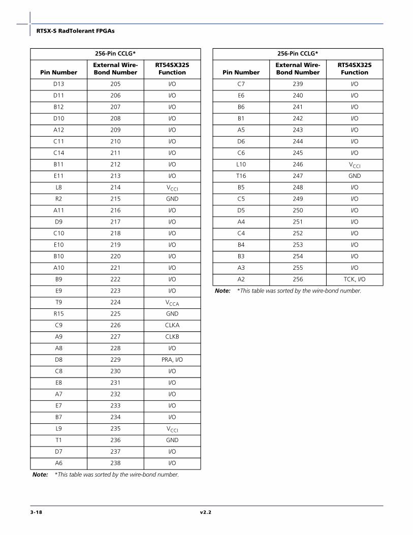
RTSX-S RadTolerant FPGAs
D13 205 I/O
D11 206 I/O
B12 207 I/O
D10 208 I/O
A12 209 I/O
C11 210 I/O
C14 211 I/O
B11 212 I/O
E11 213 I/O
L8 214 VCCI
R2 215 GND
A11 216 I/O
D9 217 I/O
C10 218 I/O
E10 219 I/O
B10 220 I/O
A10 221 I/O
B9 222 I/O
E9 223 I/O
T9 224 VCCA
R15 225 GND
C9 226 CLKA
A9 227 CLKB
A8 228 I/O
D8 229 PRA, I/O
C8 230 I/O
E8 231 I/O
A7 232 I/O
E7 233 I/O
B7 234 I/O
L9 235 VCCI
T1 236 GND
D7 237 I/O
A6 238 I/O
256-Pin CCLG*
Pin NumberExternal Wire-Bond Number
RT54SX32S Function
Note: *This table was sorted by the wire-bond number.
C7 239 I/O
E6 240 I/O
B6 241 I/O
B1 242 I/O
A5 243 I/O
D6 244 I/O
C6 245 I/O
L10 246 VCCI
T16 247 GND
B5 248 I/O
C5 249 I/O
D5 250 I/O
A4 251 I/O
C4 252 I/O
B4 253 I/O
B3 254 I/O
A3 255 I/O
A2 256 TCK, I/O
256-Pin CCLG*
Pin NumberExternal Wire-Bond Number
RT54SX32S Function
Note: *This table was sorted by the wire-bond number.
3-18 v2.2
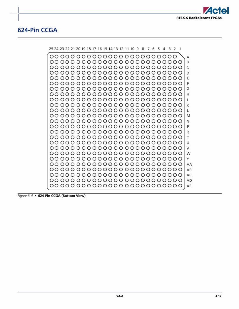
RTSX-S RadTolerant FPGAs
624-Pin CCGA
Figure 3-4 • 624-Pin CCGA (Bottom View)
25 24 23 22 21 20 19 18 17 16 15 14 13 12 11 10 9 8 7 6 5 4 3 2 1
ABC
DEFG
HJKLM
NPRTUVWY
AA
ACAB
ADAE
v2.2 3-19
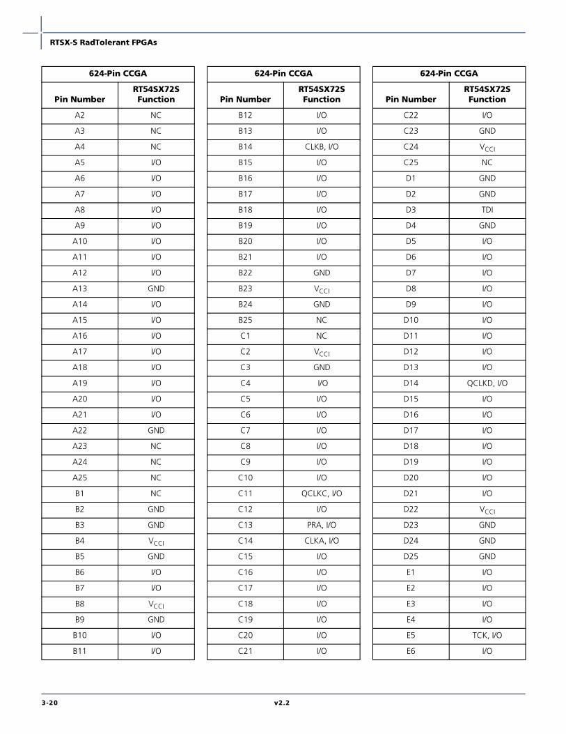
RTSX-S RadTolerant FPGAs
624-Pin CCGA
Pin NumberRT54SX72SFunction
A2 NC
A3 NC
A4 NC
A5 I/O
A6 I/O
A7 I/O
A8 I/O
A9 I/O
A10 I/O
A11 I/O
A12 I/O
A13 GND
A14 I/O
A15 I/O
A16 I/O
A17 I/O
A18 I/O
A19 I/O
A20 I/O
A21 I/O
A22 GND
A23 NC
A24 NC
A25 NC
B1 NC
B2 GND
B3 GND
B4 VCCI
B5 GND
B6 I/O
B7 I/O
B8 VCCI
B9 GND
B10 I/O
B11 I/O
B12 I/O
B13 I/O
B14 CLKB, I/O
B15 I/O
B16 I/O
B17 I/O
B18 I/O
B19 I/O
B20 I/O
B21 I/O
B22 GND
B23 VCCI
B24 GND
B25 NC
C1 NC
C2 VCCI
C3 GND
C4 I/O
C5 I/O
C6 I/O
C7 I/O
C8 I/O
C9 I/O
C10 I/O
C11 QCLKC, I/O
C12 I/O
C13 PRA, I/O
C14 CLKA, I/O
C15 I/O
C16 I/O
C17 I/O
C18 I/O
C19 I/O
C20 I/O
C21 I/O
624-Pin CCGA
Pin NumberRT54SX72SFunction
C22 I/O
C23 GND
C24 VCCI
C25 NC
D1 GND
D2 GND
D3 TDI
D4 GND
D5 I/O
D6 I/O
D7 I/O
D8 I/O
D9 I/O
D10 I/O
D11 I/O
D12 I/O
D13 I/O
D14 QCLKD, I/O
D15 I/O
D16 I/O
D17 I/O
D18 I/O
D19 I/O
D20 I/O
D21 I/O
D22 VCCI
D23 GND
D24 GND
D25 GND
E1 I/O
E2 I/O
E3 I/O
E4 I/O
E5 TCK, I/O
E6 I/O
624-Pin CCGA
Pin NumberRT54SX72SFunction
3-20 v2.2
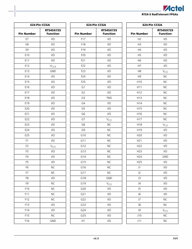
RTSX-S RadTolerant FPGAs
E7 I/O
E8 I/O
E9 I/O
E10 I/O
E11 I/O
E12 VCCA
E13 GND
E14 I/O
E15 I/O
E16 I/O
E17 I/O
E18 I/O
E19 I/O
E20 I/O
E21 I/O
E22 I/O
E23 I/O
E24 I/O
E25 I/O
F1 I/O
F2 VCCI
F3 I/O
F4 I/O
F5 I/O
F6 NC
F7 NC
F8 I/O
F9 NC
F10 NC
F11 NC
F12 NC
F13 I/O
F14 I/O
F15 NC
F16 GND
624-Pin CCGA
Pin NumberRT54SX72SFunction
F17 I/O
F18 I/O
F19 I/O
F20 I/O
F21 I/O
F22 I/O
F23 I/O
F24 I/O
F25 I/O
G1 I/O
G2 I/O
G3 TMS
G4 I/O
G5 I/O
G6 I/O
G7 VCCI
G8 NC
G9 NC
G10 NC
G11 NC
G12 NC
G13 NC
G14 NC
G15 NC
G16 NC
G17 NC
G18 GND
G19 VCCI
G20 I/O
G21 I/O
G22 I/O
G23 I/O
G24 I/O
G25 I/O
H1 I/O
624-Pin CCGA
Pin NumberRT54SX72SFunction
H2 I/O
H3 I/O
H4 I/O
H5 I/O
H6 I/O
H7 I/O
H8 VCCI
H9 NC
H10 NC
H11 NC
H12 NC
H13 NC
H14 NC
H15 NC
H16 NC
H17 NC
H18 VCCI
H19 I/O
H20 I/O
H21 I/O
H22 I/O
H23 I/O
H24 GND
H25 I/O
J1 I/O
J2 I/O
J3 I/O
J4 I/O
J5 I/O
J6 I/O
J7 NC
J8 NC
J9 VCCI
J10 NC
J11 NC
624-Pin CCGA
Pin NumberRT54SX72SFunction
v2.2 3-21
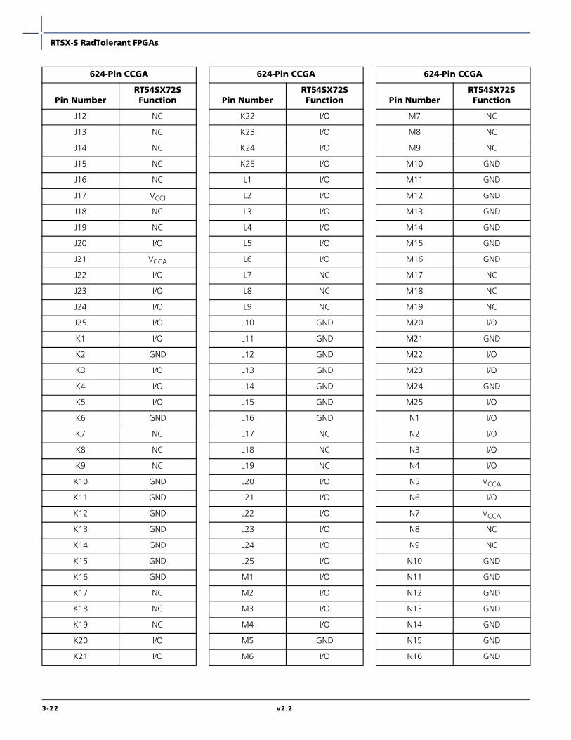
RTSX-S RadTolerant FPGAs
J12 NC
J13 NC
J14 NC
J15 NC
J16 NC
J17 VCCI
J18 NC
J19 NC
J20 I/O
J21 VCCA
J22 I/O
J23 I/O
J24 I/O
J25 I/O
K1 I/O
K2 GND
K3 I/O
K4 I/O
K5 I/O
K6 GND
K7 NC
K8 NC
K9 NC
K10 GND
K11 GND
K12 GND
K13 GND
K14 GND
K15 GND
K16 GND
K17 NC
K18 NC
K19 NC
K20 I/O
K21 I/O
624-Pin CCGA
Pin NumberRT54SX72SFunction
K22 I/O
K23 I/O
K24 I/O
K25 I/O
L1 I/O
L2 I/O
L3 I/O
L4 I/O
L5 I/O
L6 I/O
L7 NC
L8 NC
L9 NC
L10 GND
L11 GND
L12 GND
L13 GND
L14 GND
L15 GND
L16 GND
L17 NC
L18 NC
L19 NC
L20 I/O
L21 I/O
L22 I/O
L23 I/O
L24 I/O
L25 I/O
M1 I/O
M2 I/O
M3 I/O
M4 I/O
M5 GND
M6 I/O
624-Pin CCGA
Pin NumberRT54SX72SFunction
M7 NC
M8 NC
M9 NC
M10 GND
M11 GND
M12 GND
M13 GND
M14 GND
M15 GND
M16 GND
M17 NC
M18 NC
M19 NC
M20 I/O
M21 GND
M22 I/O
M23 I/O
M24 GND
M25 I/O
N1 I/O
N2 I/O
N3 I/O
N4 I/O
N5 VCCA
N6 I/O
N7 VCCA
N8 NC
N9 NC
N10 GND
N11 GND
N12 GND
N13 GND
N14 GND
N15 GND
N16 GND
624-Pin CCGA
Pin NumberRT54SX72SFunction
3-22 v2.2
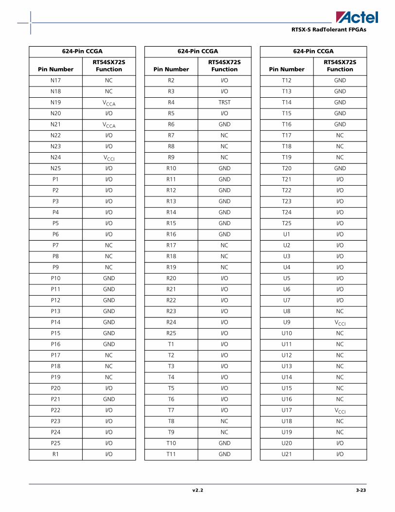
RTSX-S RadTolerant FPGAs
N17 NC
N18 NC
N19 VCCA
N20 I/O
N21 VCCA
N22 I/O
N23 I/O
N24 VCCI
N25 I/O
P1 I/O
P2 I/O
P3 I/O
P4 I/O
P5 I/O
P6 I/O
P7 NC
P8 NC
P9 NC
P10 GND
P11 GND
P12 GND
P13 GND
P14 GND
P15 GND
P16 GND
P17 NC
P18 NC
P19 NC
P20 I/O
P21 GND
P22 I/O
P23 I/O
P24 I/O
P25 I/O
R1 I/O
624-Pin CCGA
Pin NumberRT54SX72SFunction
R2 I/O
R3 I/O
R4 TRST
R5 I/O
R6 GND
R7 NC
R8 NC
R9 NC
R10 GND
R11 GND
R12 GND
R13 GND
R14 GND
R15 GND
R16 GND
R17 NC
R18 NC
R19 NC
R20 I/O
R21 I/O
R22 I/O
R23 I/O
R24 I/O
R25 I/O
T1 I/O
T2 I/O
T3 I/O
T4 I/O
T5 I/O
T6 I/O
T7 I/O
T8 NC
T9 NC
T10 GND
T11 GND
624-Pin CCGA
Pin NumberRT54SX72SFunction
T12 GND
T13 GND
T14 GND
T15 GND
T16 GND
T17 NC
T18 NC
T19 NC
T20 GND
T21 I/O
T22 I/O
T23 I/O
T24 I/O
T25 I/O
U1 I/O
U2 I/O
U3 I/O
U4 I/O
U5 I/O
U6 I/O
U7 I/O
U8 NC
U9 VCCI
U10 NC
U11 NC
U12 NC
U13 NC
U14 NC
U15 NC
U16 NC
U17 VCCI
U18 NC
U19 NC
U20 I/O
U21 I/O
624-Pin CCGA
Pin NumberRT54SX72SFunction
v2.2 3-23
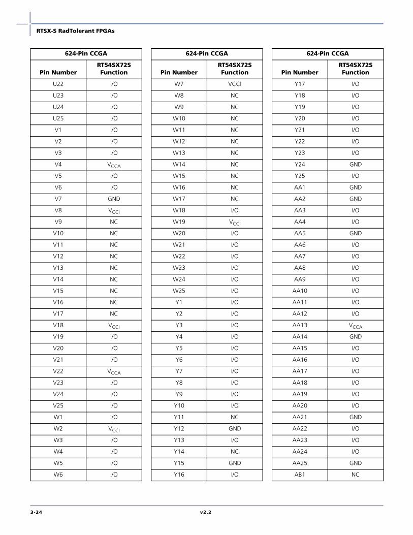
RTSX-S RadTolerant FPGAs
U22 I/O
U23 I/O
U24 I/O
U25 I/O
V1 I/O
V2 I/O
V3 I/O
V4 VCCA
V5 I/O
V6 I/O
V7 GND
V8 VCCI
V9 NC
V10 NC
V11 NC
V12 NC
V13 NC
V14 NC
V15 NC
V16 NC
V17 NC
V18 VCCI
V19 I/O
V20 I/O
V21 I/O
V22 VCCA
V23 I/O
V24 I/O
V25 I/O
W1 I/O
W2 VCCI
W3 I/O
W4 I/O
W5 I/O
W6 I/O
624-Pin CCGA
Pin NumberRT54SX72SFunction
W7 VCCI
W8 NC
W9 NC
W10 NC
W11 NC
W12 NC
W13 NC
W14 NC
W15 NC
W16 NC
W17 NC
W18 I/O
W19 VCCI
W20 I/O
W21 I/O
W22 I/O
W23 I/O
W24 I/O
W25 I/O
Y1 I/O
Y2 I/O
Y3 I/O
Y4 I/O
Y5 I/O
Y6 I/O
Y7 I/O
Y8 I/O
Y9 I/O
Y10 I/O
Y11 NC
Y12 GND
Y13 I/O
Y14 NC
Y15 GND
Y16 I/O
624-Pin CCGA
Pin NumberRT54SX72SFunction
Y17 I/O
Y18 I/O
Y19 I/O
Y20 I/O
Y21 I/O
Y22 I/O
Y23 I/O
Y24 GND
Y25 I/O
AA1 GND
AA2 GND
AA3 I/O
AA4 I/O
AA5 GND
AA6 I/O
AA7 I/O
AA8 I/O
AA9 I/O
AA10 I/O
AA11 I/O
AA12 I/O
AA13 VCCA
AA14 GND
AA15 I/O
AA16 I/O
AA17 I/O
AA18 I/O
AA19 I/O
AA20 I/O
AA21 GND
AA22 I/O
AA23 I/O
AA24 I/O
AA25 GND
AB1 NC
624-Pin CCGA
Pin NumberRT54SX72SFunction
3-24 v2.2
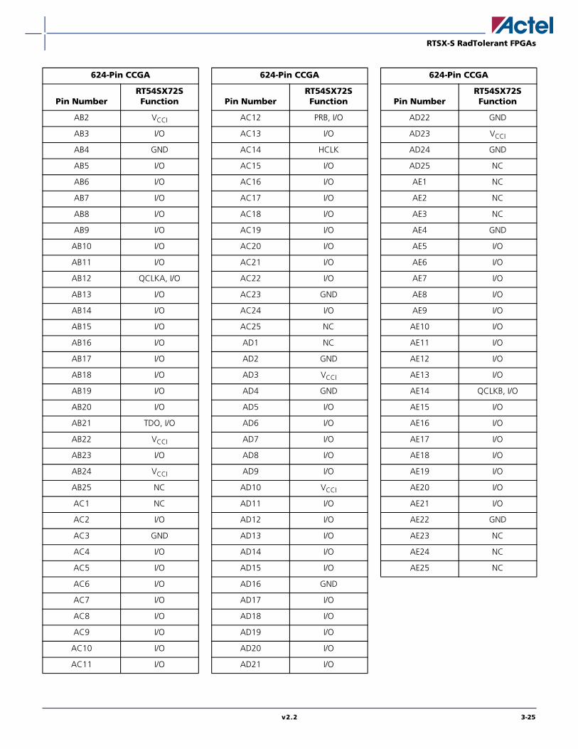
RTSX-S RadTolerant FPGAs
AB2 VCCI
AB3 I/O
AB4 GND
AB5 I/O
AB6 I/O
AB7 I/O
AB8 I/O
AB9 I/O
AB10 I/O
AB11 I/O
AB12 QCLKA, I/O
AB13 I/O
AB14 I/O
AB15 I/O
AB16 I/O
AB17 I/O
AB18 I/O
AB19 I/O
AB20 I/O
AB21 TDO, I/O
AB22 VCCI
AB23 I/O
AB24 VCCI
AB25 NC
AC1 NC
AC2 I/O
AC3 GND
AC4 I/O
AC5 I/O
AC6 I/O
AC7 I/O
AC8 I/O
AC9 I/O
AC10 I/O
AC11 I/O
624-Pin CCGA
Pin NumberRT54SX72SFunction
AC12 PRB, I/O
AC13 I/O
AC14 HCLK
AC15 I/O
AC16 I/O
AC17 I/O
AC18 I/O
AC19 I/O
AC20 I/O
AC21 I/O
AC22 I/O
AC23 GND
AC24 I/O
AC25 NC
AD1 NC
AD2 GND
AD3 VCCI
AD4 GND
AD5 I/O
AD6 I/O
AD7 I/O
AD8 I/O
AD9 I/O
AD10 VCCI
AD11 I/O
AD12 I/O
AD13 I/O
AD14 I/O
AD15 I/O
AD16 GND
AD17 I/O
AD18 I/O
AD19 I/O
AD20 I/O
AD21 I/O
624-Pin CCGA
Pin NumberRT54SX72SFunction
AD22 GND
AD23 VCCI
AD24 GND
AD25 NC
AE1 NC
AE2 NC
AE3 NC
AE4 GND
AE5 I/O
AE6 I/O
AE7 I/O
AE8 I/O
AE9 I/O
AE10 I/O
AE11 I/O
AE12 I/O
AE13 I/O
AE14 QCLKB, I/O
AE15 I/O
AE16 I/O
AE17 I/O
AE18 I/O
AE19 I/O
AE20 I/O
AE21 I/O
AE22 GND
AE23 NC
AE24 NC
AE25 NC
624-Pin CCGA
Pin NumberRT54SX72SFunction
v2.2 3-25

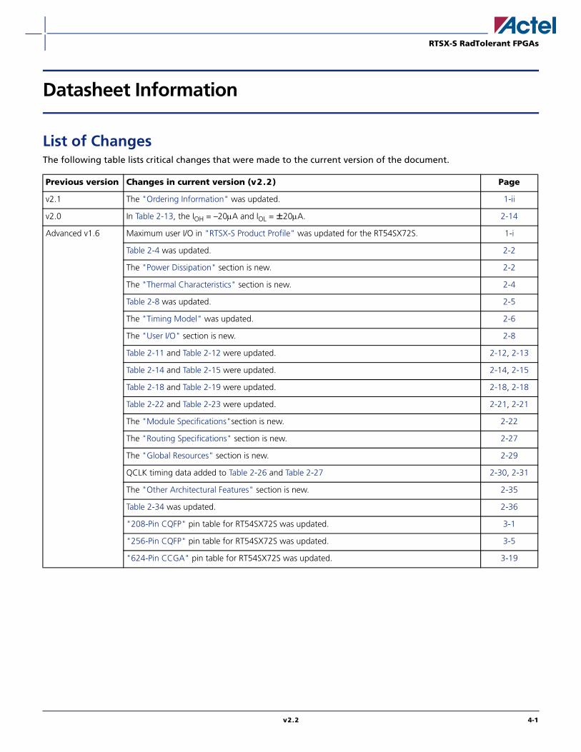
RTSX-S RadTolerant FPGAs
Datasheet Information
List of ChangesThe following table lists critical changes that were made to the current version of the document.
Previous version Changes in current version (v2.2) Page
v2.1 The "Ordering Information" was updated. 1-ii
v2.0 In Table 2-13, the IOH = –20µA and IOL = ±20µA. 2-14
Advanced v1.6 Maximum user I/O in "RTSX-S Product Profile" was updated for the RT54SX72S. 1-i
Table 2-4 was updated. 2-2
The "Power Dissipation" section is new. 2-2
The "Thermal Characteristics" section is new. 2-4
Table 2-8 was updated. 2-5
The "Timing Model" was updated. 2-6
The "User I/O" section is new. 2-8
Table 2-11 and Table 2-12 were updated. 2-12, 2-13
Table 2-14 and Table 2-15 were updated. 2-14, 2-15
Table 2-18 and Table 2-19 were updated. 2-18, 2-18
Table 2-22 and Table 2-23 were updated. 2-21, 2-21
The "Module Specifications"section is new. 2-22
The "Routing Specifications" section is new. 2-27
The "Global Resources" section is new. 2-29
QCLK timing data added to Table 2-26 and Table 2-27 2-30, 2-31
The "Other Architectural Features" section is new. 2-35
Table 2-34 was updated. 2-36
"208-Pin CQFP" pin table for RT54SX72S was updated. 3-1
"256-Pin CQFP" pin table for RT54SX72S was updated. 3-5
"624-Pin CCGA" pin table for RT54SX72S was updated. 3-19
v2.2 4-1
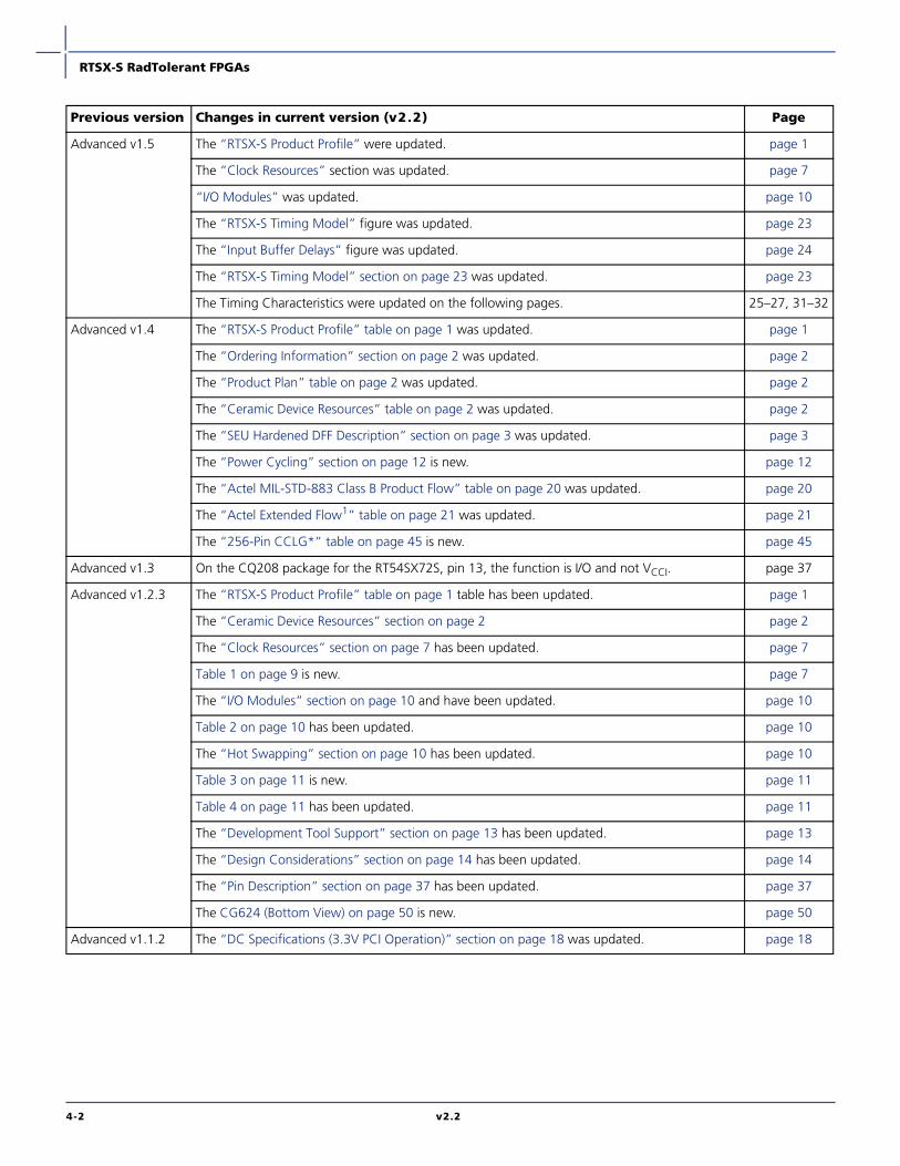
RTSX-S RadTolerant FPGAs
Advanced v1.5 The “RTSX-S Product Profile” were updated. page 1
The “Clock Resources” section was updated. page 7
“I/O Modules” was updated. page 10
The “RTSX-S Timing Model” figure was updated. page 23
The “Input Buffer Delays” figure was updated. page 24
The “RTSX-S Timing Model” section on page 23 was updated. page 23
The Timing Characteristics were updated on the following pages. 25–27, 31–32
Advanced v1.4 The “RTSX-S Product Profile” table on page 1 was updated. page 1
The “Ordering Information” section on page 2 was updated. page 2
The “Product Plan” table on page 2 was updated. page 2
The “Ceramic Device Resources” table on page 2 was updated. page 2
The “SEU Hardened DFF Description” section on page 3 was updated. page 3
The “Power Cycling” section on page 12 is new. page 12
The “Actel MIL-STD-883 Class B Product Flow” table on page 20 was updated. page 20
The “Actel Extended Flow1” table on page 21 was updated. page 21
The “256-Pin CCLG*” table on page 45 is new. page 45
Advanced v1.3 On the CQ208 package for the RT54SX72S, pin 13, the function is I/O and not VCCI. page 37
Advanced v1.2.3 The “RTSX-S Product Profile” table on page 1 table has been updated. page 1
The “Ceramic Device Resources” section on page 2 page 2
The “Clock Resources” section on page 7 has been updated. page 7
Table 1 on page 9 is new. page 7
The “I/O Modules” section on page 10 and have been updated. page 10
Table 2 on page 10 has been updated. page 10
The “Hot Swapping” section on page 10 has been updated. page 10
Table 3 on page 11 is new. page 11
Table 4 on page 11 has been updated. page 11
The “Development Tool Support” section on page 13 has been updated. page 13
The “Design Considerations” section on page 14 has been updated. page 14
The “Pin Description” section on page 37 has been updated. page 37
The CG624 (Bottom View) on page 50 is new. page 50
Advanced v1.1.2 The “DC Specifications (3.3V PCI Operation)” section on page 18 was updated. page 18
Previous version Changes in current version (v2.2) Page
4-2 v2.2
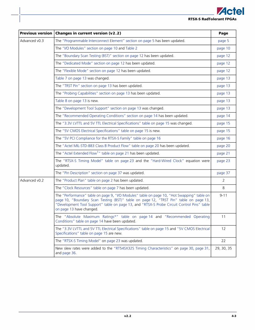
RTSX-S RadTolerant FPGAs
Advanced v0.3 The “Programmable Interconnect Element” section on page 5 has been updated. page 5
The “I/O Modules” section on page 10 and Table 2 page 10
The “Boundary Scan Testing (BST)” section on page 12 has been updated. page 12
The “Dedicated Mode” section on page 12 has been updated. page 12
The “Flexible Mode” section on page 12 has been updated. page 12
Table 7 on page 13 was changed. page 13
The “TRST Pin” section on page 13 has been updated. page 13
The “Probing Capabilities” section on page 13 has been updated. page 13
Table 8 on page 13 is new. page 13
The “Development Tool Support” section on page 13 was changed. page 13
The “Recommended Operating Conditions” section on page 14 has been updated. page 14
The “3.3V LVTTL and 5V TTL Electrical Specifications” table on page 15 was changed. page 15
The “5V CMOS Electrical Specifications” table on page 15 is new. page 15
The “5V PCI Compliance for the RTSX-S Family” table on page 16 page 16
The “Actel MIL-STD-883 Class B Product Flow” table on page 20 has been updated. page 20
The “Actel Extended Flow1” table on page 21 has been updated. page 21
The “RTSX-S Timing Model” table on page 23 and the “Hard-Wired Clock” equation wereupdated.
page 23
The “Pin Description” section on page 37 was updated. page 37
Advanced v0.2 The “Product Plan” table on page 2 has been updated. 2
The “Clock Resources” table on page 7 has been updated. 8
The “Performance” table on page 9, “I/O Modules” table on page 10, “Hot Swapping” table onpage 10, “Boundary Scan Testing (BST)” table on page 12, “TRST Pin” table on page 13,“Development Tool Support” table on page 13, and “RTSX-S Probe Circuit Control Pins” tableon page 13 have changed.
9-11
The “Absolute Maximum Ratings*” table on page 14 and “Recommended OperatingConditions” table on page 14 have been updated.
11
The “3.3V LVTTL and 5V TTL Electrical Specifications” table on page 15 and “5V CMOS ElectricalSpecifications” table on page 15 are new.
12
The “RTSX-S Timing Model” on page 23 was updated. 22
New slew rates were added to the “RT54SX32S Timing Characteristics” on page 30, page 31,and page 36.
29, 30, 35
Previous version Changes in current version (v2.2) Page
v2.2 4-3
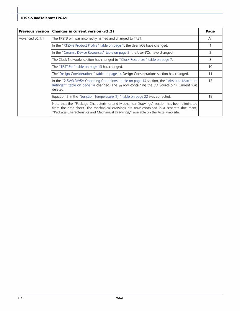
RTSX-S RadTolerant FPGAs
Advanced v0.1.1 The TRSTB pin was incorrectly named and changed to TRST. All
In the “RTSX-S Product Profile” table on page 1, the User I/Os have changed. 1
In the “Ceramic Device Resources” table on page 2, the User I/Os have changed. 2
The Clock Networks section has changed to “Clock Resources” table on page 7. 8
The “TRST Pin” table on page 13 has changed. 10
The“Design Considerations” table on page 14 Design Considerations section has changed. 11
In the “2.5V/3.3V/5V Operating Conditions” table on page 14 section, the “Absolute MaximumRatings*” table on page 14 changed. The IIO row containing the I/O Source Sink Current wasdeleted.
12
Equation 2 in the “Junction Temperature (TJ)” table on page 22 was corrected. 15
Note that the “Package Characteristics and Mechanical Drawings” section has been eliminatedfrom the data sheet. The mechanical drawings are now contained in a separate document,“Package Characteristics and Mechanical Drawings,” available on the Actel web site.
Previous version Changes in current version (v2.2) Page
4-4 v2.2
RTSX-S RadTolerant FPGAs
Datasheet CategoriesIn order to provide the latest information to designers, some datasheets are published before data has been fullycharacterized. Datasheets are designated as "Product Brief," "Advanced," "Production," and "DatasheetSupplement." The definitions of these categories are as follows:
Product BriefThe product brief is a summarized version of a datasheet (advanced or production) containing general productinformation. This brief gives an overview of specific device and family information.
AdvancedThis datasheet version contains initial estimated information based on simulation, other products, devices, or speedgrades. This information can be used as estimates, but not for production.
Unmarked (production) This datasheet version contains information that is considered to be final.
Datasheet SupplementThe datasheet supplement gives specific device information for a derivative family that differs from the general familydatasheet. The supplement is to be used in conjunction with the datasheet to obtain more detailed information andfor specifications that do not differ between the two families.
v2.2 4-5
5172151-11/11.04
http://www.actel.com
Actel and the Actel logo are registered trademarks of Actel Corporation.All other trademarks are the property of their owners.
Actel Corporation
2061 Stierlin CourtMountain View, CA94043-4655 USAPhone 650.318.4200Fax 650.318.4600
Actel Europe Ltd.
Dunlop House, Riverside WayCamberley, Surrey GU15 3YLUnited KingdomPhone +44 (0) 1276 401 450Fax +44 (0) 1276 401 490
Actel Japan
EXOS Ebisu Bldg. 4F1-24-14 Ebisu Shibuya-kuTokyo 150 JapanPhone +81.03.3445.7671Fax +81.03.3445.7668
Actel Hong Kong
39th Floor, One Pacific Place88 Queensway, AdmiraltyHong Kong Phone +852.227.35712Fax +852.227.35999