Embed Size (px)
Citation preview
Inno
Features
10G802for�SM
Elecspe
127Rec
2-wspe
Par
Line
Advenctran
RO
oLight Tech
Gb/s�serial�o2.3ae�10GBA
bi-directioF�
ctrical� inteecifications�
70/1330nm�ceiver,�integ
wire�interfacecifications�
rt�number�(0
– TR-DX1
– TR-DX3
e�side,�clien
vanced� firmcryption� innsceiver�
HS�complia
hnology Cor
optical�inteASE-ER,�sinnal�applicat
rface� comp�
DFB� tgrated�WDM
ce�for�manacompliant�w
0°C�to�70°C
12E-N00,�12
33E-N00,�13
nt�side�loop
mware� allownformation�
ant�
10Gb
TR-D
10GBAS
rp.
rface�compgle�LC�conntion,�over40
pliant� to� S
transmitter,M�
agement�with�SFF�84
C):��
270TX/1330
330TX/1270
pback�functi
w� customerto� be� st
b/s SFP+
DXxxE-N00
E-ER/EW
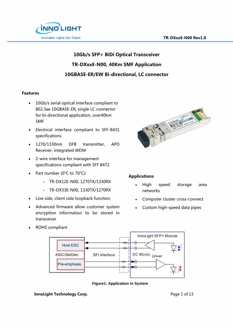
Figure1
pliant�to�nector�0km�
SFF-8431�
,� APD�
472��
0RX�
0RX�
ion;�
r� system�ored� in�
BiDi Opti
0, 40Km S
Bi-directi
1: Applicatio
Applicati
Hne
Co
Cu
ical Trans
SMF Appl
ional, LC c
on in System
TR
ions
igh� speeetworks�
omputer�clu
ustom�high
sceiver
ication
connecto
m
Page�1�of
R-DXxxE-N
ed� storag
uster�cross-
h-speed�dat
r
f�13�
00 Rev1.0
ge� area�
-connect�
ta�pipes�

Inno
1. G
Thisover
The�The�linesredulow�150
The�dataTrandisaopeensuvariaTX_FtranTX_FVcc_inputran4.7�k
The�An�oan� oconthostsuppsigninstaindior�a
�
oLight Tech
GENERAL D
s�10Gigabit�r�single�mo
SFP+�BiDi�transmitte
s� are� internuce� differenEMI.�SFI�ty
mm�of�stan
transmittea� compliannsmit�Disabable� the� laration.� � Thure� constaations.� � AnFault� is� m
nsmitter� hasFault� outpu_Host�in�theut� contact.�nsmitter�outkΩ�to�10�kΩ
receiver�coopen�collecoptical� signtact� is�an�ot� with� a� reply�filtering
nal� is� intenalled� that�cation�typic�powered�o
hnology Cor
ESCRIPTIO
SFP+�BiDi�ode�optical�f
module�eler�input�andnally� AC� contial� to� compically�ope
ndard�FR4�w
r�converts�1nt� with� theble�(Tx_Dis)�aser� from�e� transmitt
ant� optical�n� open� coodule� outps� detected�ut� contact�e�host�with
When� TX_tput�shall�b�resistor�
onverts�10Gctor�compatnal� level� beopen�drain/esistor� in� thg�is�recommded� as� a� pthe� receivecally�pointsoff�transmit
rp.
ON
transceiverfiber�for�lin
ectrical�inted�receiver�ooupled.� � Thmmon� modrates�over�2
with�one�co
10Gbit/s�see� 10GBASE
is�providedtransmittin
ter� has� an�power� ou
ollector� comput� contaca� fault� conis� an� open
h�a�resistor�_Disable� is�
be�turned�o
Gbit/s�serialtible�Loss�oelow� that� s/collector�ohe� range� 4mended�forpreliminary�ed� signal� ss�to�non-instter�at�the�fa
r�is�designek�length�40
erface�is�cooutput�impehe� module�de� conversi200�mm�of�nnector.�
erial�PECL�oE-ER� standd.� �Logic�
ng.� � Logic�internal� au
utput� acrompatible� Tct� that� whndition� relan� drain/colin�the�rangasserted� h
off.�This�con
l�optical�datof�Signal�is�pspecified� in
output�and�.7-10� kΩ,� o
r�both�the�tindication
strength� is�stalled�cablear�end�of�th
ed�to�transm0km.�
mpliant�to�edance�is�1
provides� dion� for� quaimproved�
r�CML�electard.� � An�
“1”�or�no�“0”� on�
utomatic� pooss� supply�Transmit� Fahen� high,� iated� to� laselector� and�
ge�4.7-10�khigh� or� lef
ntact�shall�b
ta�into�seriaprovided.��Rn� the� relev
shall�be�puor� with� an�transmitter�� to� the� sysbelow� the
es,�broken�he�cable.�
TR
mit�and�rec
SFI�electric100�Ohms�ddifferential�ality� signal�FR4�materia
trical�data�iopen� colleconnectionthis� pin� p
ower� controvoltage� a
ault� (Tx_Fauindicates� ter� operation
shall� be� pΩ.���TX_Disft� open,� thbe�pulled�u
al�PECL/CMRx_LOS�wheant� standaulled�up�toactive� termand�receiv
stem� in� whe� specified�cables,�or�a
Page�2�of
R-DXxxE-N
ceive�optica
cal�specificadifferential.�
terminatioterminatio
al�or�up�to�
into�serial�oector� compn�on�this�pprovides� nol� loop� (AP
and� tempeult)� is� prohat� the� mn� or� safetypulled� up� tsable�is�a�mhe� SFP+� mup�to�VccT�w
ML�electricaen�high�indrd.� � The� R
o�Vcc_Host�mination.� �ver.� ��The�Rhich� the� SF
range.� Sua�disabled,�f
f�13�
00 Rev1.0
al�data�
ations.���Data�
n� and�n� and�about�
optical�patible�in�will�
normal�PC)� to�rature�vided.��
module�y.� � The�to� the�
module�module�
with�a�
l�data.��dicates�Rx_LOS�
in�the�Power�
Rx_LOS�FP+� is�ch� an�failing�
Inno
2. P
oLight Tech
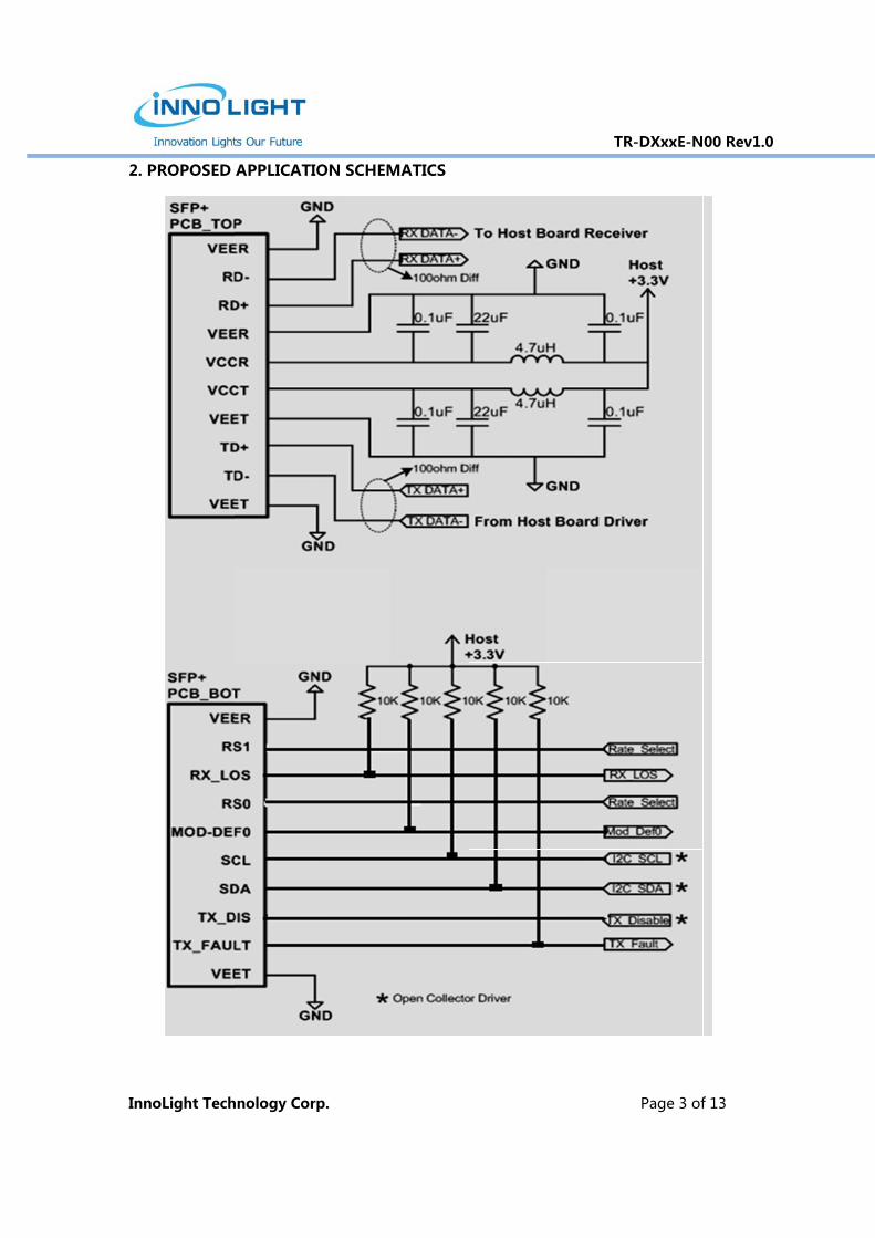
PROPOSED
hnology Cor
APPLICATI
rp.
ION SCHEM
MATICS
TR
Page�3�of
R-DXxxE-N
f�13�
00 Rev1.0
Inno
3. P
The�unp0.8�staccontSFPby�s
oLight Tech
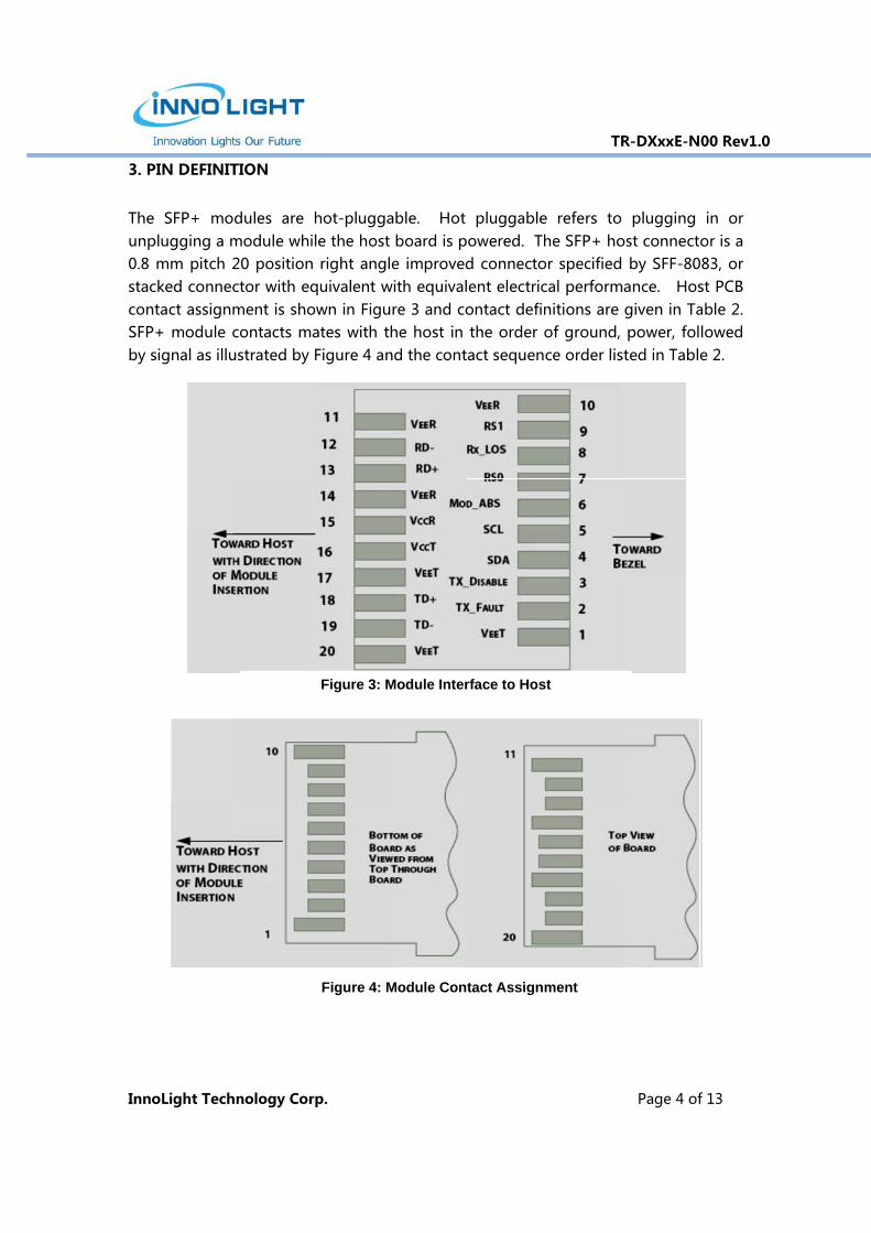
PIN DEFINIT
SFP+� moplugging�a�m
mm�pitch�2cked�connectact�assignm+�module�c
signal�as�illu
hnology Cor
TION
dules� are�module�whi20�positionctor�with�eqment�is�shocontacts�m
ustrated�by�
rp.
hot-pluggaile�the�host
n�right�anglquivalent�wown�in�Figuates�with�tFigure�4�an
Figure 4: M
Figure 3: M
able.� � Hot�t�board�is�ple� improved
with�equivalure�3�and�cothe�host� in�nd�the�cont
Module Con
Module Inter
pluggablepowered.��Thd�connectolent�electricontact�definthe�order�o
tact�sequen
tact Assign
rface to Hos
TR
e� refers� to�he�SFP+�ho
or�specifiedcal�performnitions�are�of�ground,�ce�order�lis
ment
st
Page�4�of
R-DXxxE-N
plugging�ost�connect�by�SFF-80
mance.���Hosgiven�in�Tapower,� fol
sted�in�Tabl
f�13�
00 Rev1.0
in� or�or�is�a�
083,�or�st�PCB�able�2.���lowed�e�2.�
Inno
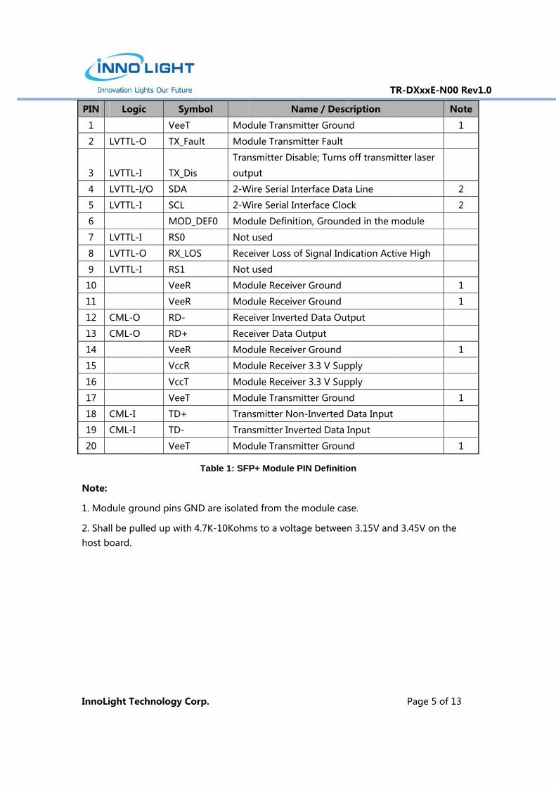
PIN
1�
2�
3�
4�
5�
6�
7�
8�
9�
10�
11�
12�
13�
14�
15�
16�
17�
18�
19�
20�
Not
1.�M
2.�Shhost
oLight Tech
Logic
��
LVTTL-O�
LVTTL-I��
LVTTL-I/O
LVTTL-I��
��
LVTTL-I��
LVTTL-O�
LVTTL-I��
��
��
CML-O��
CML-O��
��
��
��
��
CML-I��
CML-I��
��
e:
Module�grou
hall�be�pullet�board.�
hnology Cor
Sym
VeeT��
� TX_Fau
TX_Dis�
O� SDA��
SCL��
MOD_D
RS0��
� RX_LOS
RS1��
VeeR��
VeeR��
RD-�
RD+��
VeeR��
VccR��
VccT��
VeeT��
TD+�
TD-��
VeeT��
nd�pins�GN
ed�up�with�4
rp.
bol
Mod
lt�� Mod
�
Tran
out
2-W
2-W
DEF0�� Mod
Not
S�� Rec
Not
Mod
Mod
Rec
Rec
Mod
Mod
Mod
Mod
Tran
Tran
Mod
Table 1: SF
D�are�isolate
4.7K-10Kohm
N
dule�Transm
dule�Transm
nsmitter�Dis
put��
Wire�Serial�In
Wire�Serial�In
dule�Definit
t�used�
eiver�Loss�o
t�used�
dule�Receive
dule�Receive
eiver�Inverte
eiver�Data�O
dule�Receive
dule�Receive
dule�Receive
dule�Transm
nsmitter�No
nsmitter�Inv
dule�Transm
FP+ Module P
ed�from�the
ms�to�a�volta
Name / Desc
mitter�Groun
mitter�Fault�
sable;�Turns�
nterface�Dat
nterface�Cloc
tion,�Ground
of�Signal�Ind
er�Ground�
er�Ground�
ed�Data�Out
Output�
er�Ground�
er�3.3�V�Sup
er�3.3�V�Sup
mitter�Groun
on-Inverted�
verted�Data�I
mitter�Groun
PIN Definitio
e�module�cas
age�between
TR
cription
nd��
off�transmit
a�Line��
ck�
ded�in�the�m
dication�Acti
tput��
pply��
pply��
nd��
Data�Input��
Input�
nd��
on
se.�
n�3.15V�and
Page�5�of
R-DXxxE-N
tter�laser�
module��
ve�High�
d�3.45V�on�th
f�13�
00 Rev1.0
Note
1�
��
��
2�
2�
��
��
��
��
1�
1�
��
��
1�
��
��
1�
��
��
1�
he�
Inno
4. T
5. A
Thesof� tdamOpe
6. R
Recoand�
Pow
Pow
Op
Tem
oLight Tech
RANSCEIV
ABSOLUTE M
se�values�rethe� individ
mage� to� therating�Con
Power�Sup
Storage�Te
Operating�
Relative�Hu
RX�Input�A
RECOMMEN
ommendedoptical�cha
Paramet
wer�Supply�
wer�Supply�
perating�Cas
mperature,�N
hnology Cor
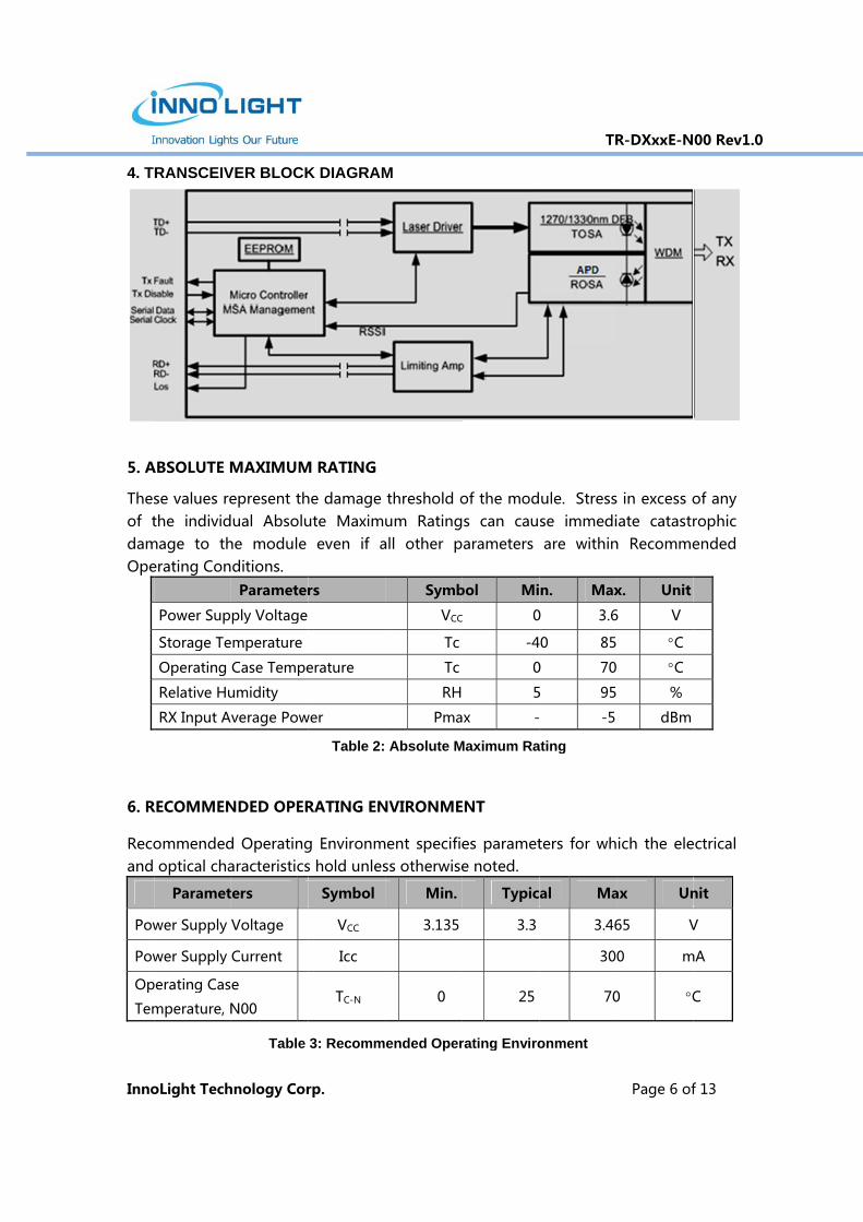
VER BLOCK
MAXIMUM
epresent�thual� Absolu
he� module�ditions.�Parameter
ply�Voltage�
mperature��
Case�Tempe
umidity�
verage�Pow
NDED OPER
d� Operatingaracteristics
ters
Voltage�
Current�
e�
N00�
Table
rp.
K DIAGRAM
M RATING
he�damage�ute� Maxim
even� if� a
rs
erature�
wer�
RATING EN
g� Environms�hold�unles
Symbol
VCC�
Icc�
TC-N�
3: Recomm
Table 2:
M
threshold�oum� Rating
all� other� p
Symb
VCC
Tc
Tc
RH
Pma
NVIRONME
ment� specifiess�otherwise
Min.
3.135
0�
ended Oper
Absolute M
of�the�mods� can� cauarameters�
bol Mi
C� 0
-4
0
5
x� -
ENT
es� paramete�noted.
Typic
3.3
25
rating Enviro
Maximum Ra
TR
ule.��Stressse� immediare� within
n. Max
0� 3.6
40� 85
0� 70
5� 95
� -5�
ters� for� wh
al Ma
3.46
30
70
onment
ating
Page�6�of
R-DXxxE-N
s�in�excess�oiate� catastr
n� Recomme
x. Unit
6� V�
� C�
� C�
� %�
dBm�
ich� the� ele
ax Un
65� V
0� m
0� C
f�13�
00 Rev1.0
of�any�rophic�ended�
ectrical�
nit
V�
mA�
C�
Inno
7. O
The�Envi
Ope
Cent
TR-D
TR-D
Side
Supp
Laun
Aver
Laun
OMA
OMA
Aver
pow
tran
Extin
RIN�
Opti
Tole
Cent
TR-D
TR-D
Rece
Rece
oLight Tech
OPTICAL CH
following�ironment�u
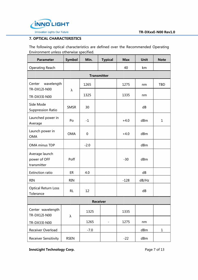
Parameter
erating�Reac
ter� wavele
DX12I-N00�
DX33I-N00�
e�Mode�
pression�Ra
nched�powe
rage�
nch�power�in
A�
A�minus�TD
rage�launch
wer�of�OFF�
smitter�
nction�ratio�
ical�Return�L
erance�
ter� wavelen
DX12I-N00�
DX33I-N00�
eiver�Overlo
eiver�Sensiti
hnology Cor
HARACTERI
optical� chanless�other
r Sym
ch�
ength�
tio�SM
er�in�P
n�OM
P�
�
Po
E
R
Loss�R
ngth�
λ
oad�
ivity� RSE
rp.
ISTICS
aracteristicsrwise�specif
mbol M
λ�
126
132
MSR� 30
Po� -1
MA� 0
� -2.
off�
ER� 4.0
RIN�
RL� 12
λ�13
12
-
EN�
s� are� defineied.�
in. Typ
Transmitte
65�
25�
0�
1�
0�
0�
2�
Receiver
325�
265�
7.0�
ed� over� the
pical M
er
1
1
+
+
-
-
1
-� 1
-
TR
e� Recomme
Max U
40�
1275�
1335�
+4.0� d
+4.0� d
� d
-30� d
128� d
1335�
1275�
d
-22� d
Page�7�of
R-DXxxE-N
ended� Ope
Unit N
km�
nm� T
nm�
dB�
dBm�
dBm�
dBm�
dBm�
dB�
B/Hz�
dB�
nm�
dBm�
dBm�
f�13�
00 Rev1.0
erating�
Note
TBD�
�
1�
�
�
�
�
1�
Inno
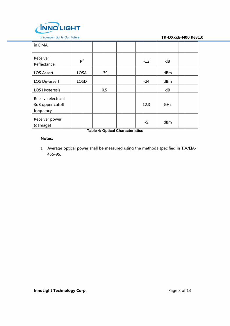
in�O
ReceRefle
LOS�
LOS�
LOS�
Rece3dB�freq
Rece(dam
N
1
�
oLight Tech
OMA�
eiver�ectance�
Assert�
De-assert�
Hysteresis�
eive�electricupper�cutouency�
eiver�power�mage)�
Notes:
1. Average455-95.�
hnology Cor
R
LOS
LOS
al�ff�
�
�
e�optical�pow
rp.
Rf�
SA� -
SD�
0
Table 4: O
wer�shall�be
-39�
0.5�
�
Optical Cha
e�measured�
-
-
�1
racteristics
using�the�m
TR
-12�
d
-24� d
12.3� G
-5� d
methods�spe
Page�8�of
R-DXxxE-N
dB�
dBm�
dBm�
dB�
GHz�
dBm�
ecified�in�TIA
f�13�
00 Rev1.0
�
�
�
A/EIA-
Inno
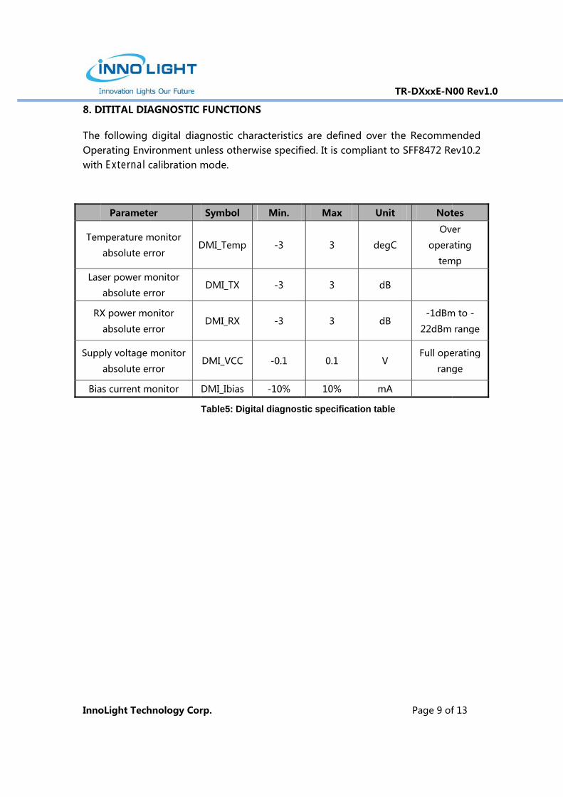
8. D
The�Opewith
�
Tem
Las
RX
Supp
Bia
oLight Tech
DITITAL DIA
following�erating�Envih�External�c
Paramete
mperature�m
absolute�er
ser�power�m
absolute�er
X�power�mo
absolute�er
ply�voltage�
absolute�er
as�current�m
hnology Cor
AGNOSTIC
digital� diagironment�ucalibration�m
er
monitor�
rror�D
monitor�
rror�
onitor�
rror�
monitor�
rror�
monitor�
T
rp.
FUNCTION
gnostic� chanless�othermode.�
Symbol
DMI_Temp
DMI_TX�
DMI_RX�
DMI_VCC�
DMI_Ibias
Table5: Digi
NS
aracteristicsrwise�specif
Min.
-3�
-3�
-3�
-0.1�
-10%�
ital diagnos
s� are� definefied.�It�is�co
Max
3�
3�
3�
0.1�
10%�
tic specifica
TR
ed� over� thempliant�to�
Unit
degC
dB�
dB�
V�
mA�
ation table
Page�9�of
R-DXxxE-N
e� RecommeSFF8472�Re
Not
Ove
opera
tem
��
-1dBm
22dBm�
Full�ope
rang
��
f�13�
00 Rev1.0
ended�ev10.2�
tes
er�
ating�
mp�
m�to�-
range
erating�
ge�
Inno
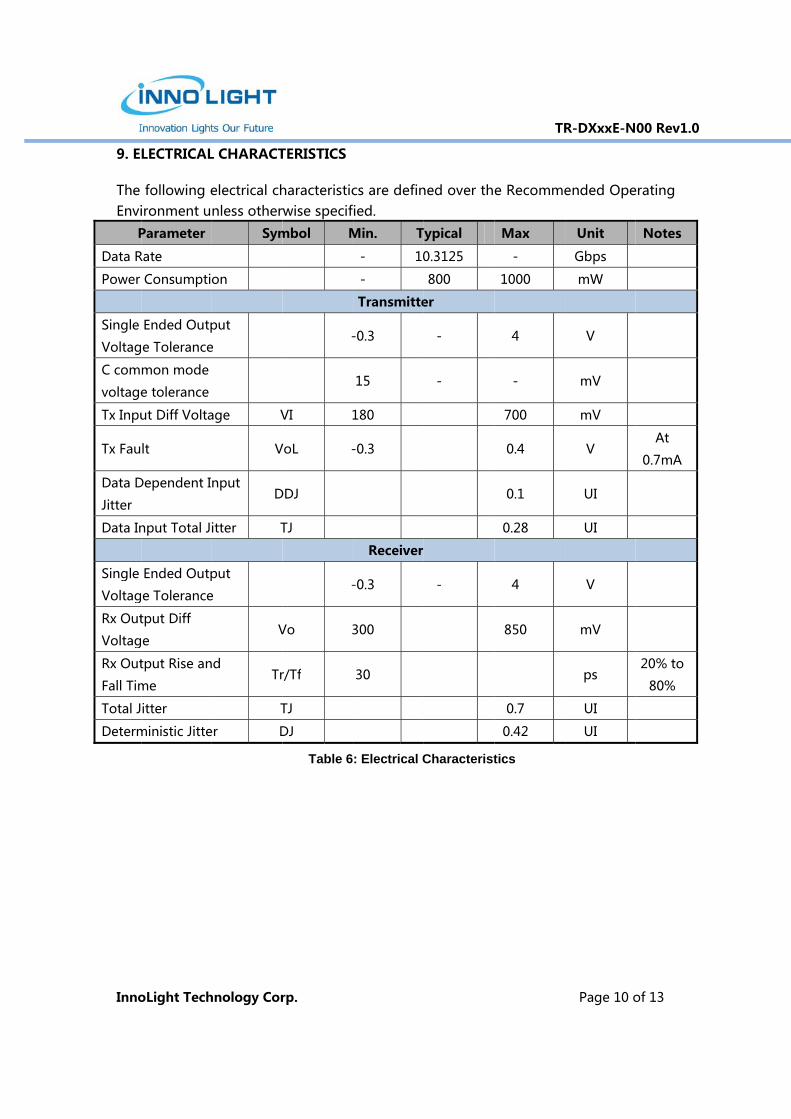
9. E
The�Envi
P
Data�R
Power�
Single�
Voltag
C�com
voltage
Tx�Inpu
Tx�Fau
Data�D
Jitter�
Data�In
Single�
Voltag
Rx�Out
Voltag
Rx�Out
Fall�Tim
Total�J
Determ
oLight Tech
LECTRICAL
following�eironment�u
Parameter
Rate�
Consumptio
Ended�Outp
e�Tolerance
mon�mode�
e�tolerance�
ut�Diff�Volta
lt�
Dependent�I
nput�Total�Ji
Ended�Outp
e�Tolerance
tput�Diff�
e�
tput�Rise�an
me�
itter�
ministic�Jitte
hnology Cor
L CHARACT
electrical�chnless�other
Sym
on�
put�
e�
age� V
V
nput�D
itter� T
put�
e�
V
d�Tr
T
er� D
rp.
TERISTICS
haracteristicrwise�specif
mbol M
�-
�
VI� 1
VoL� -
DDJ�
TJ�
�-
Vo� 3
r/Tf�
TJ�
DJ�
Table 6
cs�are�definied.�
Min. T
-� 10
-�
Transmitte
-0.3�
15�
180�
-0.3�
�
Receiver
-0.3�
300�
30�
: Electrical C
ned�over�th
Typical
0.3125�
800�
er
-�
-�
�
�
-�
�
�
Characterist
TR
e�Recomme
Max
-�
1000�
4�
-�
700�
0.4�
0.1�
0.28�
4�
850�
�
0.7�
0.42�
tics
Page�10�o
R-DXxxE-N
ended�Ope
Unit
Gbps�
mW�
V�
mV�
mV�
V�
UI�
UI�
V�
mV�
ps�
UI�
UI�
of�13�
00 Rev1.0
erating�
Notes
�
�
At�
0.7mA�
�
�
�
20%�to�
80%�
Inno
10.
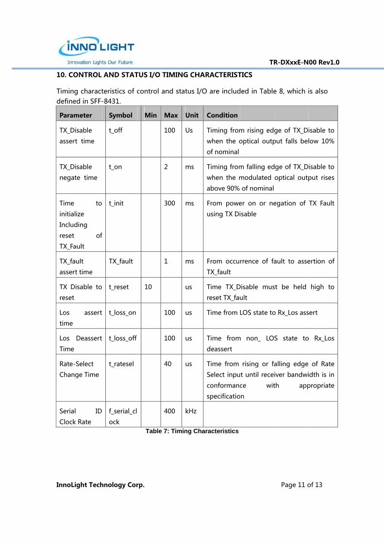
Timdefi
Par
TX_
ass
TX_
neg
Tim
init
Inc
rese
TX_
TX_
ass
TX�
rese
Los
tim
Los
Tim
Rat
Cha
Ser
Clo
oLight Tech
CONTROL
ing�charactned�in�SFF-
rameter
_Disable�
ert��time�
_Disable�
gate��time�
me� to�
tialize�
luding�
et� of�
_Fault�
_fault�
ert�time�
Disable� to�
et��
s� assert�
me�
s� Deassert�
me�
te-Select�
ange�Time�
rial� ID�
ock�Rate�
hnology Cor
AND STAT
teristics�of�c-8431.�
Symbol
t_off�
t_on�
t_init�
TX_fault�
t_reset�
t_loss_on�
t_loss_off�
t_ratesel�
f_serial_cl
ock�
rp.
TUS I/O TIM
control�and
Min Ma
� 10
� 2
� 30
� 1
10� �
� 10
� 10
� 40
� 40
Table 7: T
MING CHAR
d�status�I/O
ax Unit
0� Us�
ms�
0� ms�
ms�
us�
0� us�
0� us�
� us�
0� kHz�
Timing Char
RACTERIST
O�are�includ
Condition
Timing� from
when� the� o
of�nominal
Timing�from
when� the� m
above�90%�
From� powe
using�TX�Di
From� occu
TX_fault�
Time� TX_D
reset�TX_fau
Time�from�
Time� from
deassert�
Time� from�
Select� inpu
conformanc
specificatio
�
racteristics
TR
TICS
ded�in�Table
m� rising� edg
optical� outp
m�falling�ed
modulated�
of�nominal�
er� on� or� ne
isable�
rrence� of� fa
Disable� mus
ult��
LOS�state�to
m� non_� LO
rising� or� fa
t�until�recei
ce� wit
on�
Page�11�o
R-DXxxE-N
e�8,�which�i
ge� of� TX_Di
put� falls� bel
dge�of�TX_D
optical� outp
egation� of�
ault� to� asse
st� be� held�
o�Rx_Los�ass
S� state� to
alling� edge�
iver�bandwi
th� app
of�13�
00 Rev1.0
is�also�
isable� to�
low� 10%�
isable�to�
put� rises�
TX� Fault�
ertion� of�
high� to�
sert�
o� Rx_Los�
of� Rate�
idth�is� in�
propriate�
Inno
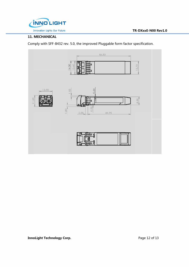
11.
Com
�
oLight Tech
MECHANIC
mply�with�SF
hnology Cor
CAL
FF-8432�rev
rp.
v.�5.0,�the�im
mproved�Pl
uggable�fo
TR
rm�factor�s
Page�12�o
R-DXxxE-N
pecification
of�13�
00 Rev1.0
n.�
Inno
12.
�
ThiselecHowmodrem
13. L
This
with
date
oLight Tech
ESD �
s� transceivectrical�inputwever,� normdule.� This�oved�from�
LASER SA
s is a Class
21 CFR 10
ed (June 24
Inn
Emai
AddressSun
hnology Cor
er� is� specifit�pins,�testemal� ESD� ptransceiverthe�packag
AFTY
1 Laser Pr
040.10 and
, 2007)
USA
oLight�Tech
Tel:�(408)�59
Fax:�(408)�59
l:��omok@in
s:�1237�East�nnyvale,�CA�
rp.
ied� as� ESD�ed�per�MIL-Sprecautions�r� is� shippeging�and�ha
roduct acco
1040.11 ex
A
hnology�Inc.
98-4238�
98-4201�
nnolight.com
Arques�Ave94085,�USA
Cont
threshold�STD-883,�M
are� still� red� in� ESD�andled�only�
ording to IEC
xcept for dev
Inn
m��
enue,��
AdS
act Informat
1kV� for� SFMethod�301required� du
protectivein�an�ESD�p
C 60825-1:2
viations purs
noLight�Tech
Tel:�(05
Fax:�(05
Email:�sale
ddress:328�XSuzhou�Indu
Jiangsu,
tion
TR
FI� pin� and�5.4�/JESD22
uring� the�e� packaginprotected�e
2007. This
suant to La
China
hnology�(Suz
12)�8666-92
12)�8666-92
es@innoligh
Xinghu�Streeustrial�Park,�S
�215123,�Ch
Page�13�o
R-DXxxE-N
2kv� for� all�2-A114-A�(handling� og.� It� shou
environmen
product com
ser Notice N
zhou)�Ltd.�
288�
299�
t.com�
et,�12-A3,�Suzhou,�
hina�
of�13�
00 Rev1.0
other�HBM).��
of� this�uld� be�nt.����
mplies
No. 50,