Embed Size (px)
Citation preview
Technical Manual
CMOS 8-BIT SINGLE CHIP MICROCOMPUTER
S1C88349 Technical Hardware
S1C88349

NOTICE
No part of this material may be reproduced or duplicated in any form or by any means without the written permission of SeikoEpson. Seiko Epson reserves the right to make changes to this material without notice. Seiko Epson does not assume anyliability of any kind arising out of any inaccuracies contained in this material or due to its application or use in any product orcircuit and, further, there is no representation that this material is applicable to products requiring high level reliability, suchas medical products. Moreover, no license to any intellectual property rights is granted by implication or otherwise, and thereis no representation or warranty that anything made in accordance with this material will be free from any patent or copyrightinfringement of a third party. This material or portions thereof may contain technology or the subject relating to strategicproducts under the control of the Foreign Exchange and Foreign Trade Law of Japan and may require an export license fromthe Ministry of International Trade and Industry or other approval from another government agency.
© SEIKO EPSON CORPORATION 2004, All rights reserved.
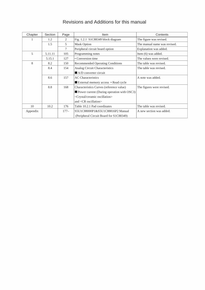
Revisions and Additions for this manual
Section
1.2
1.5
5.11.11
5.15.1
8.2
8.4
8.6
8.8
10.2
Page
2
5
7
105
127
150
154
157
168
176
177–
Item
Fig. 1.2.1 S1C88349 block diagram
Mask Option
Peripheral circuit board option
Programming notes
• Conversion time
Recommended Operating Conditions
Analog Circuit Characteristics
A/D converter circuit
AC Characteristics
External memory access • Read cycle
Characteristics Curves (reference value)
Power current (During operation with OSC3)
<Crystal/ceramic oscillation>
and <CR oscillation>
Table 10.2.1 Pad coordinates
S5U1C88000P1&S5U1C88816P2 Manual
(Peripheral Circuit Board for S1C88349)
Contents
The figure was revised.
The manual name was revised.
Explanation was added.
Item (6) was added.
The values were revised.
The table was revised.
The table was revised.
A note was added.
The figures were revised.
The table was revised.
A new section was added.
Chapter
1
5
8
10
Appendix


DevicesS1 C 88104 F 0A01
Packing specifications 00: Besides tape & reel0A: TCP BL 2 directions0B: Tape & reelBACK0C: TCP BR 2 directions0D: TCP BT 2 directions0E: TCP BD 2 directions0F: Tape & reelFRONT0G: TCP BT 4 directions0H: TCP BD 4 directions0J : TCP SL 2 directions0K: TCP SR 2 directions0L: Tape & reel LEFT0M: TCP ST 2 directions0N: TCP SD 2 directions0P: TCP ST 4 directions0Q: TCP SD 4 directions0R: Tape & reelRIGHT99 : Specs not fixed
Specification
PackageD: die form; F: QFP
Model number
Model nameC: microcomputer, digital products
Product classificationS1: semiconductor
Development toolsS5U1 C 88348 D1 1
Packing specifications 00: standard packing
Version 1: Version 1
Tool typeHx: ICEEx: EVA boardPx: Peripheral boardWx: Flash ROM writer for the microcomputerXx: ROM writer peripheral board
Cx: C compiler packageAx: Assembler packageDx: Utility tool by the modelQx: Soft simulator
Corresponding model number 88348: for S1C88348
Tool classificationC: microcomputer use
Product classification S5U1: development tool for semiconductor products
00
00
S1C88 Family
Configuration of product number

S1C88349 TECHNICAL MANUAL EPSON i
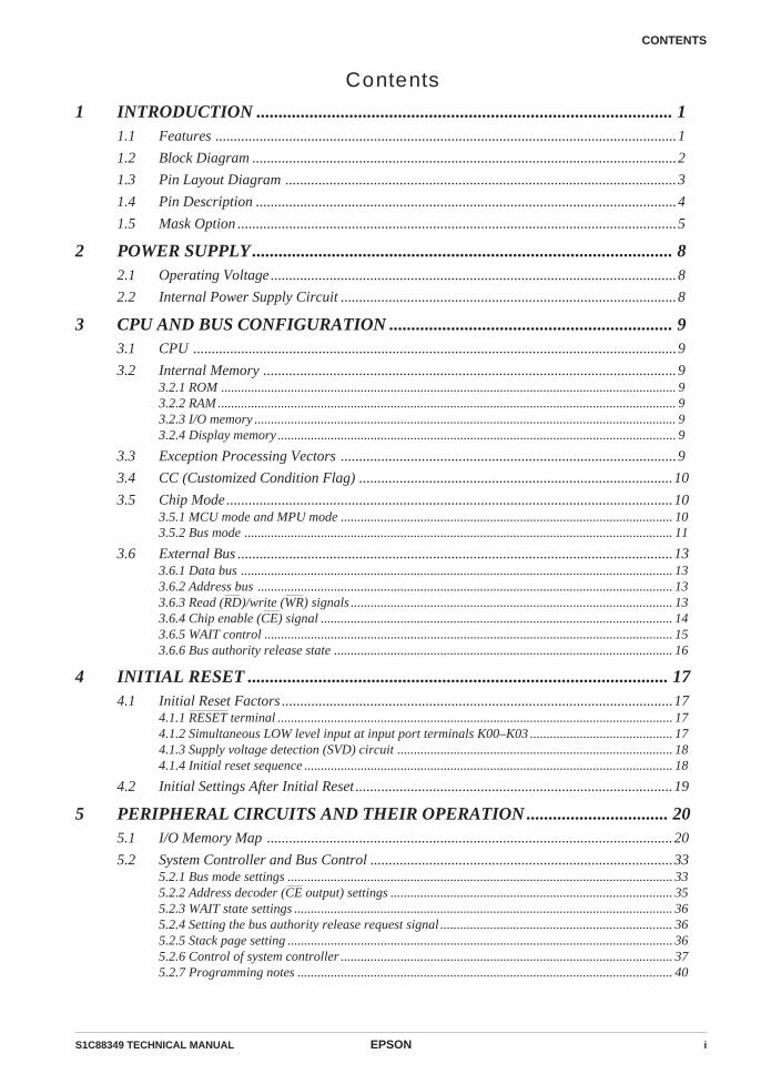
CONTENTS
Contents
1 INTRODUCTION .............................................................................................. 11.1 Features .............................................................................................................................1
1.2 Block Diagram ...................................................................................................................2
1.3 Pin Layout Diagram ..........................................................................................................3
1.4 Pin Description ..................................................................................................................4
1.5 Mask Option .......................................................................................................................5
2 POWER SUPPLY............................................................................................... 82.1 Operating Voltage ..............................................................................................................8
2.2 Internal Power Supply Circuit ...........................................................................................8
3 CPU AND BUS CONFIGURATION ................................................................ 93.1 CPU ...................................................................................................................................9
3.2 Internal Memory ................................................................................................................93.2.1 ROM ......................................................................................................................................... 93.2.2 RAM .......................................................................................................................................... 93.2.3 I/O memory ............................................................................................................................... 93.2.4 Display memory ........................................................................................................................ 9
3.3 Exception Processing Vectors ...........................................................................................9
3.4 CC (Customized Condition Flag) .....................................................................................10
3.5 Chip Mode .........................................................................................................................103.5.1 MCU mode and MPU mode .................................................................................................... 103.5.2 Bus mode ................................................................................................................................. 11
3.6 External Bus ......................................................................................................................133.6.1 Data bus .................................................................................................................................. 133.6.2 Address bus ............................................................................................................................. 133.6.3 Read (RD)/write (WR) signals ................................................................................................. 133.6.4 Chip enable (CE) signal .......................................................................................................... 143.6.5 WAIT control ........................................................................................................................... 153.6.6 Bus authority release state ...................................................................................................... 16
4 INITIAL RESET ............................................................................................... 174.1 Initial Reset Factors ..........................................................................................................17
4.1.1 RESET terminal ....................................................................................................................... 174.1.2 Simultaneous LOW level input at input port terminals K00–K03 ........................................... 174.1.3 Supply voltage detection (SVD) circuit ................................................................................... 184.1.4 Initial reset sequence ............................................................................................................... 18
4.2 Initial Settings After Initial Reset ......................................................................................19
5 PERIPHERAL CIRCUITS AND THEIR OPERATION ................................ 205.1 I/O Memory Map ..............................................................................................................20
5.2 System Controller and Bus Control ..................................................................................335.2.1 Bus mode settings .................................................................................................................... 335.2.2 Address decoder (CE output) settings ..................................................................................... 355.2.3 WAIT state settings .................................................................................................................. 365.2.4 Setting the bus authority release request signal ...................................................................... 365.2.5 Stack page setting .................................................................................................................... 365.2.6 Control of system controller .................................................................................................... 375.2.7 Programming notes ................................................................................................................. 40
ii EPSON S1C88349 TECHNICAL MANUAL
CONTENTS
5.3 Watchdog Timer ................................................................................................................415.3.1 Configuration of watchdog timer ............................................................................................ 415.3.2 Interrupt function .................................................................................................................... 415.3.3 Control of watchdog timer ...................................................................................................... 415.3.4 Programming notes ................................................................................................................. 41
5.4 Oscillation Circuits and Operating Mode ........................................................................425.4.1 Configuration of oscillation circuits ....................................................................................... 425.4.2 Mask option ............................................................................................................................. 425.4.3 OSC1 oscillation circuit .......................................................................................................... 425.4.4 OSC3 oscillation circuit .......................................................................................................... 435.4.5 Operating mode ....................................................................................................................... 435.4.6 Switching the CPU clocks ....................................................................................................... 445.4.7 Control of oscillation circuit and operating mode .................................................................. 455.4.8 Programming notes ................................................................................................................. 46
5.5 Input Ports (K ports) .........................................................................................................475.5.1 Configuration of input ports .................................................................................................... 475.5.2 Mask option ............................................................................................................................. 475.5.3 Interrupt function and input comparison register ................................................................... 485.5.4 Control of input ports .............................................................................................................. 505.5.5 Programming note ................................................................................................................... 52
5.6 Output Ports (R ports) ......................................................................................................535.6.1 Configuration of output ports .................................................................................................. 535.6.2 Mask option ............................................................................................................................. 545.6.3 High impedance control .......................................................................................................... 545.6.4 DC output ................................................................................................................................ 555.6.5 Special output .......................................................................................................................... 555.6.6 Control of output ports ............................................................................................................ 575.6.7 Programming notes ................................................................................................................. 61
5.7 I/O Ports (P ports) ............................................................................................................625.7.1 Configuration of I/O ports ....................................................................................................... 625.7.2 Mask option ............................................................................................................................. 625.7.3 I/O control registers and I/O mode ......................................................................................... 635.7.4 Control of I/O ports ................................................................................................................. 635.7.5 Programming notes ................................................................................................................. 64
5.8 Serial Interface .................................................................................................................655.8.1 Configuration of serial interface ............................................................................................. 655.8.2 Mask option ............................................................................................................................. 665.8.3 Transfer modes ........................................................................................................................ 665.8.4 Clock source ............................................................................................................................ 675.8.5 Transmit-receive control ......................................................................................................... 685.8.6 Operation of clock synchronous transfer ................................................................................ 695.8.7 Operation of asynchronous transfer ....................................................................................... 735.8.8 Interrupt function .................................................................................................................... 775.8.9 Control of serial interface ....................................................................................................... 795.8.10 Programming notes ............................................................................................................... 83
5.9 Clock Timer .......................................................................................................................845.9.1 Configuration of clock timer ................................................................................................... 845.9.2 Interrupt function .................................................................................................................... 845.9.3 Control of clock timer ............................................................................................................. 865.9.4 Programming notes ................................................................................................................. 88
5.10 Stopwatch Timer ...............................................................................................................895.10.1 Configuration of stopwatch timer ......................................................................................... 895.10.2 Count up pattern .................................................................................................................... 895.10.3 Interrupt function .................................................................................................................. 905.10.4 Control of stopwatch timer .................................................................................................... 915.10.5 Programming notes ............................................................................................................... 93
S1C88349 TECHNICAL MANUAL EPSON iii
CONTENTS
5.11 Programmable Timer ........................................................................................................945.11.1 Configuration of programmable timer .................................................................................. 945.11.2 Count operation and setting basic mode ............................................................................... 945.11.3 Setting of input clock ............................................................................................................. 965.11.4 Timer mode ............................................................................................................................ 965.11.5 Event counter mode ............................................................................................................... 975.11.6 Pulse width measurement timer mode ................................................................................... 975.11.7 Interrupt function .................................................................................................................. 985.11.8 Setting of TOUT output ......................................................................................................... 985.11.9 Transmission rate setting of serial interface ......................................................................... 995.11.10 Control of programmable timer ......................................................................................... 1005.11.11 Programming notes ............................................................................................................ 105
5.12 LCD Controller ................................................................................................................1065.12.1 Configuration of LCD controller ......................................................................................... 1065.12.2 Mask option .......................................................................................................................... 1065.12.3 Switching drive duty ............................................................................................................. 1065.12.4 LCD power supply ................................................................................................................ 1075.12.5 LCD driver ........................................................................................................................... 1075.12.6 Display memory .................................................................................................................... 1105.12.7 Display control ..................................................................................................................... 1175.12.8 CL and FR outputs ............................................................................................................... 1175.12.9 Control of LCD controller .................................................................................................... 1185.12.10 Programming notes ............................................................................................................ 120
5.13 Sound Generator ..............................................................................................................1215.13.1 Configuration of sound generator ........................................................................................ 1215.13.2 Control of buzzer output ....................................................................................................... 1215.13.3 Setting of buzzer frequency and sound level ........................................................................ 1225.13.4 Digital envelope ................................................................................................................... 1225.13.5 One-shot output .................................................................................................................... 1235.13.6 Control of sound generator .................................................................................................. 1245.13.7 Programming notes .............................................................................................................. 126
5.14 Analog Comparator .........................................................................................................1275.14.1 Configuration of analog comparator ................................................................................... 1275.14.2 Mask option .......................................................................................................................... 1275.14.3 Analog comparator operation .............................................................................................. 1275.14.4 Control of analog comparator ............................................................................................. 1285.14.5 Programming notes .............................................................................................................. 128
5.15 A/D Converter ..................................................................................................................1295.15.1 Characteristics and configuration of A/D converter ............................................................ 1295.15.2 Terminal configuration of A/D converter ............................................................................. 1295.15.3 Mask option .......................................................................................................................... 1295.15.4 A/D conversion ..................................................................................................................... 1305.15.5 Interrupt function ................................................................................................................. 1315.15.6 Control of A/D converter ...................................................................................................... 1325.15.7 Programming notes .............................................................................................................. 135
5.16 Supply Voltage Detection (SVD) Circuit .........................................................................1365.16.1 Configuration of SVD circuit ............................................................................................... 1365.16.2 Mask option .......................................................................................................................... 1365.16.3 Operation of SVD circuit ...................................................................................................... 1365.16.4 Control of SVD circuit .......................................................................................................... 1385.16.5 Programming notes .............................................................................................................. 139
5.17 Interrupt and Standby Status ...........................................................................................1405.17.1 Interrupt generation conditions ........................................................................................... 1415.17.2 Interrupt factor flag .............................................................................................................. 1415.17.3 Interrupt enable register ...................................................................................................... 1425.17.4 Interrupt priority register and interrupt priority level ......................................................... 1425.17.5 Exception processing vectors ............................................................................................... 1435.17.6 Control of interrupt .............................................................................................................. 1445.17.7 Programming notes .............................................................................................................. 145
iv EPSON S1C88349 TECHNICAL MANUAL
CONTENTS
6 SUMMARY OF NOTES .................................................................................. 1466.1 Notes for Low Current Consumption ...............................................................................146
6.2 Precautions on Mounting.................................................................................................147
7 BASIC EXTERNAL WIRING DIAGRAM ..................................................... 149
8 ELECTRICAL CHARACTERISTICS ............................................................ 1508.1 Absolute Maximum Rating ...............................................................................................150
8.2 Recommended Operating Conditions ..............................................................................150
8.3 DC Characteristics ..........................................................................................................151
8.4 Analog Circuit Characteristics ........................................................................................152
8.5 Power Current Consumption ...........................................................................................155
8.6 AC Characteristics ...........................................................................................................156
8.7 Oscillation Characteristics ..............................................................................................164
8.8 Characteristics Curves (reference value) ........................................................................165
9 PACKAGE ........................................................................................................ 1729.1 Plastic Package................................................................................................................172
9.2 Ceramic Package for Test Samples .................................................................................174
10 PAD LAYOUT .................................................................................................. 17510.1 Diagram of Pad Layout ...................................................................................................175
10.2 Pad Coordinates ..............................................................................................................176
APPENDIX S5U1C88000P1&S5U1C88816P2 MANUAL(Peripheral Circuit Board for S1C88349) ........................................... 177
A.1 Names and Functions of Each Part .................................................................................177
A.2 Installation .......................................................................................................................179A.2.1 Installing S5U1C88816P2 to S5U1C88000P1 ...................................................................... 179A2.2 Installing into the ICE (S5U1C88000H5) .............................................................................. 179
A.3 Connecting to the Target System .....................................................................................180
A.4 Downloading Circuit Data to the S5U1C88000P1 .........................................................182
A.5 Precautions ......................................................................................................................183A.5.1 Precaution for operation ....................................................................................................... 183A.5.2 Differences from actual IC .................................................................................................... 183
A.6 Product Specifications .....................................................................................................185A.6.1 S5U1C88000P1 specifications .............................................................................................. 185A.6.2 S5U1C88816P2 specifications .............................................................................................. 185
S1C88349 TECHNICAL MANUAL EPSON 1
1 INTRODUCTION
1 INTRODUCTIONThe S1C88349 microcomputer features the
S1C88 (Model 3) CMOS 8-bit core CPU along with48K bytes of ROM, 2K bytes of RAM, three differ-ent timers, a serial interface with optionalasynchronization or clock synchronization, and anA/D converter.The S1C88349 is fully operable over a wide range ofvoltages, and can perform high speed operations
even at low voltage. Like all the equipment in theS1C Family, these microcomputers have low powerconsumption.A 19-bit external address bus and 4 bits chip enablesignals make it possible for this microcomputer tocontrol up to 512K × 4 bytes of memory, makingthem ideal for high performance data bank sys-tems.
1.1 FeaturesTable 1.1.1 lists the features of the S1C88349.
Table 1.1.1 Main features
* The number of bits cited for output ports and I/O ports does not include those shared with the bus.
Core CPU
OSC1 oscillation circuit
OSC3 oscillation circuit
Instruction set
Min. instruction execution time
Internal ROM capacity
Internal RAM capacity
Bus line
Input port
Output port
I/O port
Serial interface
Timer
LCD driver
Sound generator
Watchdog timer
Analog comparator
A/D converter
Supply voltage detection
(SVD) circuit
Interrupt
Supply voltage
Current consumption
Supply form
S1C88 (MODEL3) CMOS 8-bit core CPU
Crystal oscillation circuit/CR oscillation circuit/external clock input 32.768 kHz (Typ.)
Crystal oscillation circuit/ceramic oscillation circuit/CR oscillation circuit/external clock input 8.2 MHz (Max.)
608 types (usable for multiplication and division instructions)
0.244 µsec/8.2 MHz (2 clock)
Address bus:
Data bus:
CE signal:
WR signal:
RD signal:
10 bits (2 bits can be set for event counter external clock input and bus request signal input terminal)
9 bits (6 bits can be set for buzzer output, LCD control, FOUT, TOUT and bus acknowledge signal output terminal)
48K bytes
2K bytes/RAM 3,216 bits/display memory
8 bits (4 bits each can be set for serial interface input/output and analog comparator/AD input)
1ch (optional clock synchronous system or asynchronous system)
Programmable timer (8 bits): (1ch can be set as a an event counter or 2ch as a 16 bits programmable timer for 1ch)
Clock timer (8 bits):
Stopwatch timer (8 bits):
Envelope function, equipped with volume control
Built-in
2ch built-in (not available if A/D converter is used)
Resolution: 10 bits, input: 4ch, Maximum error: ±5 LSB (not available if analog comparator is used)
Can detect up to 16 different voltage levels
External interrupt:
Internal interrupt:
Normal mode:
Low power mode:
High speed mode:
SLEEP mode: 0.3 µA
HALT mode: 1.5 µA (Typ./normal mode)
Run (32 kHz): 9 µA (Typ./normal mode)
Run (4 MHz): 1.1 mA (Typ./normal mode)
QFP18-176pin, QFP21-176pin or chip
Dot matrix type (supports5 × 8 or 5 × 5 fonts)
51 segments × 32 commons (1/5 bias)
67 segments × 16 or 8 commons (1/5 bias)
Built-in LCD power supply circuit (booster type, 5 potentials)
19 bits (also usable as a general output port when not used as a bus)
8 bits (also usable as a general I/O port when not used as a bus)
4 bits
1 bit
1 bit
(also usable as a general output port when not used as a bus)
2ch
1ch
1ch
Input interrupt
Timer interrupt
Serial interface interrupt
A/D converter interrupt
2.4 V–5.5 V (Max. 4.2 MHz)
1.8 V–3.5 V (Max. 80 kHz)
3.5 V–5.5 V (Max. 8.2 MHz)
2 systems (3 types)
3 systems (9 types)
1 system (3 types)
1 system (1 type)
VD1 = 2.2 V
VD1 = 1.2 V
VD1 = 3.3 V
2 EPSON S1C88349 TECHNICAL MANUAL
1 INTRODUCTION
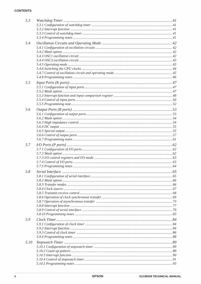
1.2 Block Diagram
Fig. 1.2.1 S1C88349 block diagram
Core CPU S1C88
Interrupt Controller
System Controller Input Port
OscillatorOSC1, 2
OSC3, 4
BREQ (K11)BACK (R51)
Reset/TestRESET
TEST
Watchdog Timer
K00–K07K10 (EVIN)K11 (BREQ)
I/O Port
Serial Interface
ExternalMemoryInterface
Output Port
Programmable Timer/Event Counter
Clock Timer
Stopwatch Timer
Power Generator
Analog Comparator/AD Converter
RAM2K byte
EVIN (K10)
P00–P07 (D0–D7)
P10 (SIN)P11 (SOUT)P12 (SCLK)P13 (SRDY)
R00–R07, R10–R17, R20–R22 (A0–A7, A8–A15, A16–A18)R23, R24 (RD, WR)R30–R33 (CE0–CE3)R25, R26 (CL, FR)R27 (TOUT)
R35–R37R50 (BZ)R51 (BACK)
MCU/MPU
Sound Generator
SEG0–SEG50COM16–COM31 (SEG66–SEG51)COM0–COM15
R34 (FOUT)
P14 (CMPP0/AD4)P15 (CMPM0/AD5)P16 (CMPP1/AD6)P17 (CMPM1/AD7)
VDD
VSS
VD1
VOSC
VC1–VC5
CA–CE
VREF
AVDD
AVSS
AVREF
LCD Driver
Supply Voltage Detector
ROM48K byte

S1C88349 TECHNICAL MANUAL EPSON 3
1 INTRODUCTION
Pin No. Pin name1234567891011121314151617181920212223242526272829303132333435363738394041424344
Pin No. Pin nameSEG46SEG47SEG48SEG49SEG50
COM31/SEG51COM30/SEG52COM29/SEG53COM28/SEG54COM27/SEG55COM26/SEG56COM25/SEG57COM24/SEG58COM23/SEG59COM22/SEG60COM21/SEG61COM20/SEG62COM19/SEG63COM18/SEG64COM17/SEG65COM16/SEG66
N.C.N.C.N.C.N.C.N.C.N.C.VREF
CECDCCCBCAVC5
VC4
VC3
VC2
VC1
OSC3OSC4VD1
VDD
VSS
VOSC
SEG2SEG3SEG4SEG5SEG6SEG7SEG8SEG9SEG10SEG11SEG12SEG13SEG14SEG15SEG16SEG17SEG18SEG19SEG20SEG21SEG22SEG23SEG24SEG25SEG26SEG27SEG28SEG29SEG30SEG31SEG32SEG33SEG34SEG35SEG36SEG37SEG38SEG39SEG40SEG41SEG42SEG43SEG44SEG45
Pin No. Pin name8990919293949596979899100101102103104105106107108109110111112113114115116117118119120121122123124125126127128129130131132
OSC1OSC2TEST
RESETMCU/MPUK11/BREQK10/EVIN
K07K06K05K04K03K02K01K00
P17/CMPM1/AD7P16/CMPP1/AD6P15/CMPM0/AD5P14/CMPP0/AD4
P13/SRDYP12/SCLKP11/SOUTP10/SINAVDD
AVSS
AVREF
VDD
P07/D7P06/D6P05/D5P04/D4P03/D3P02/D2P01/D1P00/D0R00/A0R01/A1R02/A2R03/A3R04/A4R05/A5R06/A6R07/A7R10/A8
Pin No. Pin name133134135136137138139140141142143144145146147148149150151152153154155156157158159160161162163164165166167168169170171172173174175176
R11/A9R12/A10R13/A11R14/A12R15/A13R16/A14R17/A15R20/A16R21/A17R22/A18R23/RDR24/WRR25/CLR26/FR
R27/TOUTR30/CE0R31/CE1R32/CE2R33/CE3
R34/FOUTR35R36R37VSS
R50/BZR51/BACK
COM0COM1COM2COM3COM4COM5COM6COM7COM8COM9COM10COM11COM12COM13COM14COM15SEG0SEG1
4546474849505152535455565758596061626364656667686970717273747576777879808182838485868788
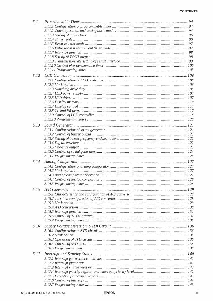
1.3 Pin Layout Diagram
QFP18-176pin QFP21-176pin
Fig. 1.3.1 S1C88349 pin layout
89132
45
88
INDEX
441
176
133
89132
45
88
INDEX
441
176
133
4 EPSON S1C88349 TECHNICAL MANUAL
1 INTRODUCTION
1.4 Pin Description
Table 1.4.1 S1C88349 pin description Pin No.
VDD
VSS
VD1
VOSC
VC1–VC5
CA–CEVREF
OSC1
OSC2OSC3
OSC4MCU/MPUK00–K07K10/EVINK11/BREQR00–R07/A0–A7R10–R17/A8–A15R20–R22/A16–A18R23/RDR24/WRR25/CLR26/FRR27/TOUT
R30–R33/CE0–CE3R34/FOUTR35–R37R50/BZR51/BACKP00–P07/D0–D7P10/SINP11/SOUTP12/SCLKP13/SRDYP14/CMPP0/AD4
P15/CMPM0/AD5
P16/CMPP1/AD6
P17/CMPM1/AD7
COM0–COM15COM16–COM31/SEG66–SEG51SEG0–SEG50RESETTESTAVDD
AVSS
AVREF
Pin name In/Out Function86, 11587, 156
8588
82–7877–73
7289
9083
8493
103–969594
124–131132–139140–142
143144145146147
148–151152
153–155157158
123–116111110109108107
106
105
104
159–17465–50
175–176, 1–499291
112113114
–––––––I
OI
OIIIIOOOOOOOO
OOOOO
I/OI/OI/OI/OI/OI/O
I/O
I/O
I/O
OO
OII–––
Power supply (+) terminalPower supply (GND) terminal Internal logic system voltage regulator output terminalOscillation system voltage regulator output terminalLCD drive voltage output terminalsBooster capacitor connection terminals for LCDLCD system power testing terminalOSC1 oscillation input terminal (select crystal oscillation/CR oscillation/external clock input by mask option)OSC1 oscillation output terminalOSC3 oscillation input terminal(select crystal/ceramic/CR oscillation/external clock input by mask option)OSC3 oscillation output terminalTerminal for setting MCU or MPU modesInput terminals (K00–K07)Input terminal (K10) or event counter external clock input terminal (EVIN)Input terminal (K11) or bus request signal input terminal (BREQ)Output terminals (R00–R07) or address bus (A0–A7)Output terminals (R10–R17) or address bus (A8–A15)Output terminals (R20–R22) or address bus (A16–A18)Output terminal (R23) or read signal output terminal (RD)Output terminal (R24) or write signal output terminal (WR)Output terminal (R25) or LCD synchronous signal output terminal (CL)Output terminal (R26) or LCD frame signal output terminal (FR) Output terminal (R27)or programmable timer underflow signal output terminal (TOUT)Output terminals (R30–R33) or chip enable output terminals (CE0–CE3)Output terminal (R34) or clock output terminal (FOUT)Output terminals (R35–R37)Output terminal (R50) or buzzer output terminal (BZ)Output terminal (R51) or bus acknowledge signal output terminal (BACK)I/O terminals (P00–P07) or data bus (D0–D7)I/O terminal (P10) or serial I/F data input terminal (SIN)I/O terminal (P11) or serial I/F data output terminal (SOUT)I/O terminal (P12) or serial I/F clock I/O terminal (SCLK)I/O terminal (P13) or serial I/F ready signal output terminal (SRDY)I/O terminal (P14), analog comparator 0 non-inverted input terminal or A/D converter input terminalI/O terminal (P15), analog comparator 0 inverted input terminalor A/D converter input terminalI/O terminal (P16), analog comparator 1 non-inverted input terminalor A/D converter input terminalI/O terminal (P17), analog comparator 1 inverted input terminalor A/D converter input terminalLCD common output terminalsLCD common output terminals (when 1/32 duty is selected)or LCD segment output terminal (when 1/16 duty is selected)LCD segment output terminalsInitial reset input terminalTest input terminalAnalog system power supply (+) terminalAnalog system power supply (–) terminalAnalog system reference voltage terminal

S1C88349 TECHNICAL MANUAL EPSON 5
1 INTRODUCTION
1.5 Mask OptionMask options shown below are provided for theS1C88349. Several hardware specifications areprepared in each mask option, and one of them canbe selected according to the application. The functionoption generator winfog, that has been prepared asthe development software tool of the S1C88349, isused for this selection. Mask pattern of the IC isfinally generated based on the data created by thewinfog. Refer to the "S5U1C88000C Manual II" fordetails on the winfog.
Option listThe following options can be set for the S1C88349and ICE (S5U1C88000H5). Multiple specificationsare available in each option item as indicated in theOption List. Select the specifications that meet thetarget system and check the appropriate box.The option selection is done interactively on thescreen during winfog execution, using this optionlist as reference.
PERIPHERAL CIRCUIT BOARD option list
A OSC1 SYSTEM CLOCK 1. Internal Clock 2. User Clock
B OSC3 SYSTEM CLOCK 1. Internal Clock 2. User Clock
S1C88349 mask option list
1 OSC1 SYSTEM CLOCK 1. Crystal 2. External Clock 3. CR 4. Crystal (with Gate Capacity)
2 OSC3 SYSTEM CLOCK 1. Crystal 2. Ceramic 3. CR 4. External Clock
3 MULTIPLE KEY ENTRY RESET• Combination ... 1. Not Use
2. Use K00, K01 3. Use K00, K01, K02 4. Use K00, K01, K02, K03
4 MPU MODE INITIAL SET 1. 512K (MAX) 2. 512K (MIN) 3. 64K
5 SVD RESET 1. Not Use 2. Use
6 EPSON S1C88349 TECHNICAL MANUAL
1 INTRODUCTION
6 INPUT PORT PULL UP RESISTOR• K00 ................... 1. With Resistor 2. Gate Direct• K01 ................... 1. With Resistor 2. Gate Direct• K02 ................... 1. With Resistor 2. Gate Direct• K03 ................... 1. With Resistor 2. Gate Direct• K04 ................... 1. With Resistor 2. Gate Direct• K05 ................... 1. With Resistor 2. Gate Direct• K06 ................... 1. With Resistor 2. Gate Direct• K07 ................... 1. With Resistor 2. Gate Direct• K10 ................... 1. With Resistor 2. Gate Direct• K11 ................... 1. With Resistor 2. Gate Direct• MCU/MPU ..... 1. With Resistor 2. Gate Direct• RESET .............. 1. With Resistor 2. Gate Direct
7 I/O PORT PULL UP RESISTOR• P00 .................... 1. With Resistor 2. Gate Direct• P01 .................... 1. With Resistor 2. Gate Direct• P02 .................... 1. With Resistor 2. Gate Direct• P03 .................... 1. With Resistor 2. Gate Direct• P04 .................... 1. With Resistor 2. Gate Direct• P05 .................... 1. With Resistor 2. Gate Direct• P06 .................... 1. With Resistor 2. Gate Direct• P07 .................... 1. With Resistor 2. Gate Direct• P10 .................... 1. With Resistor 2. Gate Direct• P11 .................... 1. With Resistor 2. Gate Direct• P12 .................... 1. With Resistor 2. Gate Direct• P13 .................... 1. With Resistor 2. Gate Direct• P14 .................... 1. With Resistor 2. Gate Direct• P15 .................... 1. With Resistor 2. Gate Direct• P16 .................... 1. With Resistor 2. Gate Direct• P17 .................... 1. With Resistor 2. Gate Direct
8 OUTPUT PORT SPECIFICATION• R00 .................... 1. Complementary 2. Nch Open Drain• R01 .................... 1. Complementary 2. Nch Open Drain• R02 .................... 1. Complementary 2. Nch Open Drain• R03 .................... 1. Complementary 2. Nch Open Drain• R04 .................... 1. Complementary 2. Nch Open Drain• R05 .................... 1. Complementary 2. Nch Open Drain• R06 .................... 1. Complementary 2. Nch Open Drain• R07 .................... 1. Complementary 2. Nch Open Drain• R10 .................... 1. Complementary 2. Nch Open Drain• R11 .................... 1. Complementary 2. Nch Open Drain• R12 .................... 1. Complementary 2. Nch Open Drain• R13 .................... 1. Complementary 2. Nch Open Drain• R14 .................... 1. Complementary 2. Nch Open Drain• R15 .................... 1. Complementary 2. Nch Open Drain• R16 .................... 1. Complementary 2. Nch Open Drain• R17 .................... 1. Complementary 2. Nch Open Drain
9 LCD POWER SUPPLY 1. Internal 2. External
S1C88349 TECHNICAL MANUAL EPSON 7
1 INTRODUCTION
Outline of mask options
Peripheral circuit board optionThese options configure the Peripheral CircuitBoard (S5U1C88000P1 with S5U1C88816P2)installed in the ICE (S5U1C88000H5). The selectionsdo not affect the IC's mask option.
(A) OSC1 system clockWhen User Clock is selected, input a clock tothe OSC1 terminal. When Internal Clock isselected, the clock frequency is changedaccording to the oscillation circuit selected bythe IC's mask option.
(B) OSC3 system clockWhen User Clock is selected, input a clock tothe OSC3 terminal. When Internal Clock isselected, the clock frequency is changedaccording to the oscillation circuit selected bythe IC's mask option.
S1C88349 mask option
(1) OSC1 oscillation circuitThe specification of the OSC1 oscillation circuitcan be selected from among four types: "Crystaloscillation", "CR oscillation", "Crystal oscillation(gate capacitor built-in)" and "External clockinput". Refer to Section 5.4.3, "OSC1 oscillationcircuit", for details.
(2) OSC3 oscillation circuitThe specification of the OSC3 oscillation circuitcan be selected from among four types: "Crystaloscillation", "Ceramic oscillation", "CR oscilla-tion" and "External clock input". Refer to Section5.4.4, "OSC3 oscillation circuit", for details.
(3) Multiple key entry reset (K00–K03)This function resets the IC when several keysare pressed simultaneously. The mask option isused to select whether this function is used ornot. Further when the function is used, acombination of the input ports (K00–K03),which are connected to the keys to be pressedsimultaneously, can be selected. Refer to Section4.1.2, "Simultaneous LOW level input at inputport terminals K00–K03", for details.
(4) Initial bus mode for MPU modeThe bus mode that is initially set in MPU modecan be selected from expanded 512K maximummode, expanded 512K minimum mode andexpanded 64K mode. Refer to Section 5.2,"System controller and Bus Control", for details.
(5) Initial reset by SVD circuitThe SVD circuit has a function that generates aninitial reset signal when the supply voltagedrops to level 0 or less. The mask option is usedto select whether this function is used or not.Refer to Section 5.16, "Supply Voltage Detection(SVD) Circuit", for details.
(6)_______ ___________
Input port, MCU/MPU and RESET terminalpull-up resistorsThis mask option can select whether the pull-upresistor for the input (K) port terminal is used ornot. It is possible to select for each bit of theinput ports. Refer to Section 5.5, "Input Ports (Kports)", for details.Furthermore, a pull-up option is also provided_______ ___________for the MCU/MPU and RESET terminals.
(7) I/O port pull-up resistorsThis mask option can select whether the pull-upresistor for the I/O port terminal (it worksduring input mode) is used or not. It is possibleto select for each bit of the I/O ports. Refer toSection 5.7, "I/O Ports (P ports)", for details.
Since P10 to P13 are shared with the serialinterface I/O terminals, the selected P10 andP12 terminal configuration is applied to theserial input (SIN) terminal and serial clock input_________terminal (SCLK in clock synchronous mode)when the serial interface is used. Refer toSection 5.8, "Serial Interface", for details.
(8) Output port specificationsEither complementary output or Nch opendrain output can be selected as the outputspecification for the output ports R00–R07 andR10–R17 in 1 bit units. Refer to Section 5.6.2,"Mask option", for details.
(9) LCD power supplyEither the internal power supply (internal LCDsystem voltage regulator and voltage boosterthat generate VC1 to VC5) or an external powersupply can be selected as the LCD systempower source. Refer to Section 5.12.2, "Maskoption", for details.

8 EPSON S1C88349 TECHNICAL MANUAL
2 POWER SUPPLY
2 POWER SUPPLYIn this section, we will explain the operating
voltage and the configuration of the internal powersupply circuit of the S1C88349.
2.1 Operating VoltageThe S1C88349 operating power voltage is asfollows:
Normal mode: 2.4 V to 5.5 VLow power mode: 1.8 V to 3.5 VHigh speed mode: 3.5 V to 5.5 V
2.2 Internal Power Supply CircuitThe S1C88349 incorporates the power supply circuitshown in Figure 2.2.1. When voltage within therange described above is supplied to VDD (+) and VSS
(GND), all the voltages needed for the internal circuitare generated internally in the IC.
Roughly speaking, the power supply circuit isdivided into three sections.
The internal logic voltage regulator generates theoperating voltage <VD1> for driving the internallogic circuits and the OSC3 oscillation circuit. TheVD1 voltage can be selected from the followingthree types: 1.2 V for low-power mode, 2.2 V fornormal mode and 3.1 V for high-speed mode.It should be selected by a program to switchaccording to the supply voltage and oscillationfrequency.See Section 5.4, "Oscillation Circuits and OperatingMode", for the switching of operating mode.
Note: Under no circumstances should VD1 terminaloutput be used to drive external circuit.
The oscillation system voltage regulator generatesthe operating voltage <VOSC> for the OSC1 oscilla-tion circuit.
The LCD system power supply circuit generates thedrive voltage for the LCD. Drive voltage has fivepotentials VC1–VC5 for 1/5 bias: VC1 and VC2 aregenerated by the LCD voltage regulator, and areboosted to generate VC3–VC5. These voltages areoutput from the terminals to drive an external LCDdriver (S1D15210 or equivalent).See Chapter 8, "ELECTRICAL CHARACTERIS-TICS" for the voltage values.
In the S1C88349, the LCD drive voltage is suppliedto the built-in LCD driver which drives the LCDpanel connected to the SEG and COM terminals.
Notes: • Do not use terminals VC1–VC5 except tosupply voltage to the expanded LCDdriver.
• Refer to the "S1D15000 Series TechnicalManual" for the S1D15210 externalyexpanded LCD driver.
Externalpowersupply
VDD
AVDD
VD1
VOSC
VC1
VC2
VREF
VC3
VC4
VC5
CACBCCCDCE
AVSS
VSS
VD1
VOSC
VC1,VC2
VC3–VC5
OSC3, OSC4
OSC1, OSC2
COM0–COM15COM16–COM31/SEG66–SEG51 SEG0–SEG50
Internal logic systemvoltage regulator
Internal voltagesetting circuit
OSC3oscillation circuit
Internal circuit
Oscillation systemvoltage regulator
OSC1oscillation circuit
LCD systemvoltage regulator
LCD systemvoltage booster LCD driver
A/D converter
Fig. 2.2.1 Configuration of power supply circuit
S1C88349 TECHNICAL MANUAL EPSON 9
3 CPU AND BUS CONFIGURATION
3 CPU AND BUS CONFIGURATIONIn this section, we will explain the CPU, operating mode and bus configuration.
3.1 CPUThe S1C88349 utilize the S1C88 8-bit core CPUwhose register configuration, command set, etc. arevirtually identical to other units in the family ofprocessors incorporating the S1C88.
See the "S1C88 Core CPU Manual" for the S1C88.
Specifically, the S1C88349 employ the Model 3S1C88 CPU which has a maximum address space of512K bytes × 4.
3.2 Internal MemoryThe S1C88349 is equipped with internal ROM andRAM as shown in Figure 3.2.1. Small scale applica-tions can be handled by one chip. It is also possibleto utilize internal memory in combination withexternal memory.Furthermore, internal ROM can be disconnectedfrom the bus and the resulting space released forexternal applications.
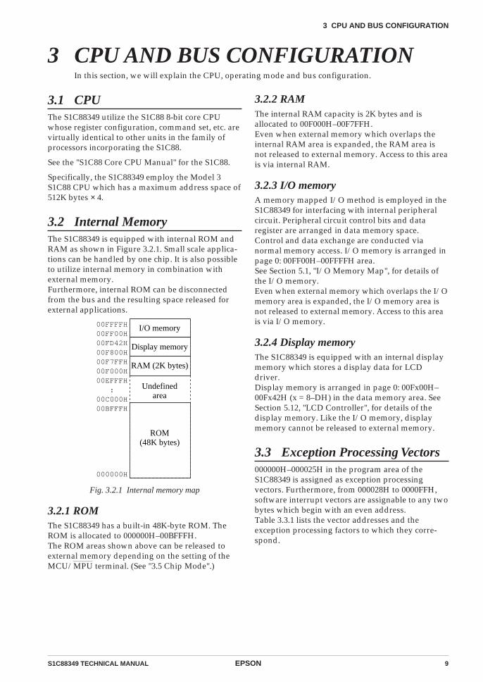
3.2.2 RAMThe internal RAM capacity is 2K bytes and isallocated to 00F000H–00F7FFH.Even when external memory which overlaps theinternal RAM area is expanded, the RAM area isnot released to external memory. Access to this areais via internal RAM.
3.2.3 I/O memoryA memory mapped I/O method is employed in theS1C88349 for interfacing with internal peripheralcircuit. Peripheral circuit control bits and dataregister are arranged in data memory space.Control and data exchange are conducted vianormal memory access. I/O memory is arranged inpage 0: 00FF00H–00FFFFH area.See Section 5.1, "I/O Memory Map", for details ofthe I/O memory.Even when external memory which overlaps the I/Omemory area is expanded, the I/O memory area isnot released to external memory. Access to this areais via I/O memory.
3.2.4 Display memoryThe S1C88349 is equipped with an internal displaymemory which stores a display data for LCDdriver.Display memory is arranged in page 0: 00Fx00H–00Fx42H (x = 8–DH) in the data memory area. SeeSection 5.12, "LCD Controller", for details of thedisplay memory. Like the I/O memory, displaymemory cannot be released to external memory.
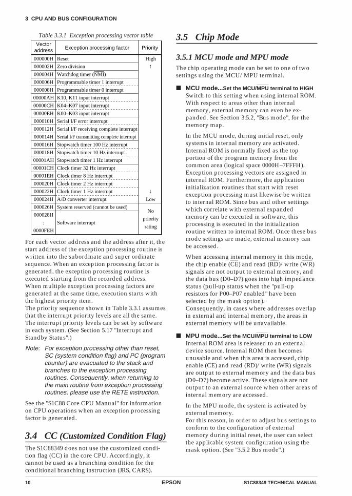
3.3 Exception Processing Vectors000000H–000025H in the program area of theS1C88349 is assigned as exception processingvectors. Furthermore, from 000028H to 0000FFH,software interrupt vectors are assignable to any twobytes which begin with an even address.Table 3.3.1 lists the vector addresses and theexception processing factors to which they corre-spond.
Fig. 3.2.1 Internal memory map
3.2.1 ROMThe S1C88349 has a built-in 48K-byte ROM. TheROM is allocated to 000000H–00BFFFH.The ROM areas shown above can be released toexternal memory depending on the setting of theMCU/MPU terminal. (See "3.5 Chip Mode".)
00FFFFH00FF00H00FD42H00F800H00F7FFH00F000H00EFFFH
:00C000H00BFFFH
000000H
I/O memory
Display memory
RAM (2K bytes)
Undefinedarea
ROM(48K bytes)
10 EPSON S1C88349 TECHNICAL MANUAL
3 CPU AND BUS CONFIGURATION
3.5 Chip Mode
3.5.1 MCU mode and MPU modeThe chip operating mode can be set to one of twosettings using the MCU/MPU terminal.
MCU mode...Set the MCU/MPU terminal to HIGHSwitch to this setting when using internal ROM.With respect to areas other than internalmemory, external memory can even be ex-panded. See Section 3.5.2, "Bus mode", for thememory map.
In the MCU mode, during initial reset, onlysystems in internal memory are activated.Internal ROM is normally fixed as the topportion of the program memory from thecommon area (logical space 0000H–7FFFH).Exception processing vectors are assigned ininternal ROM. Furthermore, the applicationinitialization routines that start with resetexception processing must likewise be writtento internal ROM. Since bus and other settingswhich correlate with external expandedmemory can be executed in software, thisprocessing is executed in the initializationroutine written to internal ROM. Once these busmode settings are made, external memory canbe accessed.
When accessing internal memory in this mode,the chip enable (CE) and read (RD)/write (WR)signals are not output to external memory, andthe data bus (D0–D7) goes into high impedancestatus (pull-up status when the "pull-upresistors for P00–P07 enabled" have beenselected by the mask option).Consequently, in cases where addresses overlapin external and internal memory, the areas inexternal memory will be unavailable.
MPU mode...Set the MCU/MPU terminal to LOWInternal ROM area is released to an externaldevice source. Internal ROM then becomesunusable and when this area is accessed, chipenable (CE) and read (RD)/write (WR) signalsare output to external memory and the data bus(D0–D7) become active. These signals are notoutput to an external source when other areas ofinternal memory are accessed.
In the MPU mode, the system is activated byexternal memory.For this reason, in order to adjust bus settings toconform to the configuration of externalmemory during initial reset, the user can selectthe applicable system configuration using themask option. (See "3.5.2 Bus mode".)
Table 3.3.1 Exception processing vector table
For each vector address and the address after it, thestart address of the exception processing routine iswritten into the subordinate and super ordinatesequence. When an exception processing factor isgenerated, the exception processing routine isexecuted starting from the recorded address.When multiple exception processing factors aregenerated at the same time, execution starts withthe highest priority item.The priority sequence shown in Table 3.3.1 assumesthat the interrupt priority levels are all the same.The interrupt priority levels can be set by softwarein each system. (See Section 5.17 "Interrupt andStandby Status".)
Note: For exception processing other than reset,SC (system condition flag) and PC (programcounter) are evacuated to the stack andbranches to the exception processingroutines. Consequently, when returning tothe main routine from exception processingroutines, please use the RETE instruction.
See the "S1C88 Core CPU Manual" for informationon CPU operations when an exception processingfactor is generated.
3.4 CC (Customized Condition Flag)The S1C88349 does not use the customized condi-tion flag (CC) in the core CPU. Accordingly, itcannot be used as a branching condition for theconditional branching instruction (JRS, CARS).
Vectoraddress
000000H
000002H
000004H
000006H
000008H
00000AH
00000CH
00000EH
000010H
000012H
000014H
000016H
000018H
00001AH
00001CH
00001EH
000020H
000022H
000024H
000026H
000028H
:
0000FEH
Priority
High
↑
↓Low
No
priority
rating
Exception processing factor
Reset
Zero division
Watchdog timer (NMI)
Programmable timer 1 interrupt
Programmable timer 0 interrupt
K10, K11 input interrupt
K04–K07 input interrupt
K00–K03 input interrupt
Serial I/F error interrupt
Serial I/F receiving complete interrupt
Serial I/F transmitting complete interrupt
Stopwatch timer 100 Hz interrupt
Stopwatch timer 10 Hz interrupt
Stopwatch timer 1 Hz interrupt
Clock timer 32 Hz interrupt
Clock timer 8 Hz interrupt
Clock timer 2 Hz interrupt
Clock timer 1 Hz interrupt
A/D converter interrupt
System reserved (cannot be used)
Software interrupt
S1C88349 TECHNICAL MANUAL EPSON 11
3 CPU AND BUS CONFIGURATION
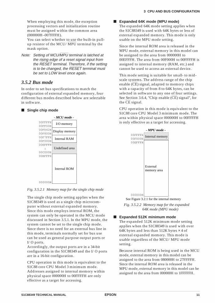
Expanded 64K mode (MPU mode)The expanded 64K mode setting applies whenthe S1C88349 is used with 64K bytes or less ofexternal expanded memory. This mode is onlyusable on the MPU mode setting.
Since the internal ROM area is released in theMPU mode, external memory in this model canbe assigned to the area from 000000H to00EFFFH. The area from 00F000H to 00FFFFH isassigned to internal memory (RAM, etc.) andcannot be used to access an external device.
This mode setting is suitable for small- to mid-scale systems. The address range of the chipenable (CE) signal, adapted to memory chipswith a capacity of from 8 to 64K bytes, can beselected in software to any one of four settings.See Section 3.6.4, "Chip enable (CE) signal", forthe CE signal.
CPU operation in this mode is equivalent to theS1C88 core CPU Model 3 minimum mode. Thearea within physical space 000000H to 00FFFFHis only effective as a target for accessing.
00FFFFH00F000H00EFFFH
000000H
See Figure 3.2.1 for the internal memory
- MPU mode -
Internal memory
Externalmemory area
Fig. 3.5.2.2 Memory map for the expanded 64K mode (MPU mode)
Expanded 512K minimum modeThe expanded 512K minimum mode settingapplies when the S1C88349 is used with over64K bytes and less than 512K bytes × 4 ofexternal expanded memory. This mode isusable regardless of the MCU/MPU modesetting.
Because internal ROM is being used in the MCUmode, external memory in this model can beassigned to the area from 080000H to 27FFFFH.Since the internal ROM area is released in theMPU mode, external memory in this model can beassigned to the area from 000000H to 1FFFFFH.
When employing this mode, the exceptionprocessing vectors and initialization routinemust be assigned within the common area(000000H–007FFFH).You can select whether to use the built-in pull-up resistor of the MCU/MPU terminal by themask option.
Note: Setting of MCU/MPU terminal is latched atthe rising edge of a reset signal input fromthe RESET terminal. Therefore, if the settingis to be changed, the RESET terminal mustbe set to LOW level once again.
3.5.2 Bus modeIn order to set bus specifications to match theconfiguration of external expanded memory, fourdifferent bus modes described below are selectablein software.
Single chip mode
Fig. 3.5.2.1 Memory map for the single chip mode
The single chip mode setting applies when theS1C88349 is used as a single chip microcom-puter without external expanded memory.Since this mode employs internal ROM, thesystem can only be operated in the MCU modediscussed in Section 3.5.1. In the MPU mode, thesystem cannot be set to the single chip mode.Since there is no need for an external bus line inthis mode, terminals normally set for bus usecan be used as general purpose output ports orI/O ports.Accordingly, the output ports are in a 34-bitconfiguration in the S1C88349 and the I/O portsare in a 16-bit configuration.
CPU operation in this mode is equivalent to theS1C88 core CPU Model 3 minimum mode.Addresses assigned to internal memory withinphysical space 000000H to 00FFFFH are onlyeffective as a target for accessing.
00FFFFH00FF00H00FD42H00F800H00F7FFH00F000H00EFFFH
:00C000H00BFFFH
000000H
- MCU mode -
I/O memory
Display memory
Internal RAM
Undefined area
Internal ROM
12 EPSON S1C88349 TECHNICAL MANUAL
3 CPU AND BUS CONFIGURATION
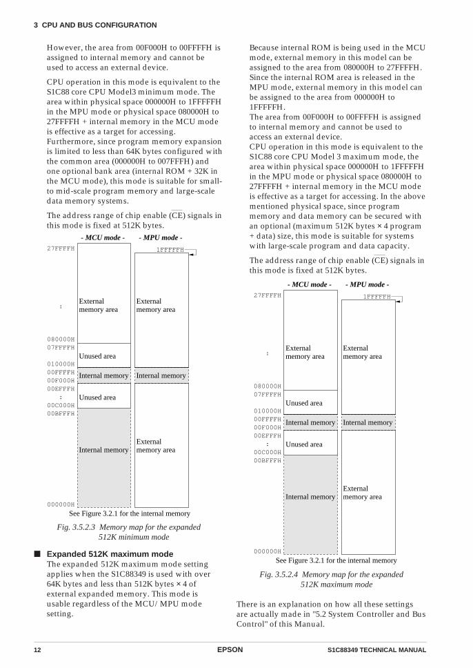
However, the area from 00F000H to 00FFFFH isassigned to internal memory and cannot beused to access an external device.
CPU operation in this mode is equivalent to theS1C88 core CPU Model3 minimum mode. Thearea within physical space 000000H to 1FFFFFHin the MPU mode or physical space 080000H to27FFFFH + internal memory in the MCU modeis effective as a target for accessing.Furthermore, since program memory expansionis limited to less than 64K bytes configured withthe common area (000000H to 007FFFH) andone optional bank area (internal ROM + 32K inthe MCU mode), this mode is suitable for small-to mid-scale program memory and large-scaledata memory systems.
The address range of chip enable (CE) signals inthis mode is fixed at 512K bytes.
Internal memory
27FFFFH
:
080000H07FFFFH
010000H00FFFFH00F000H00EFFFH
:00C000H00BFFFH
000000H
See Figure 3.2.1 for the internal memory
- MPU mode -
Externalmemory area
Internal memory
Externalmemory area
1FFFFFH
- MCU mode -
Externalmemory area
Internal memory
Unused area
Unused area
Fig. 3.5.2.3 Memory map for the expanded 512K minimum mode
Expanded 512K maximum modeThe expanded 512K maximum mode settingapplies when the S1C88349 is used with over64K bytes and less than 512K bytes × 4 ofexternal expanded memory. This mode isusable regardless of the MCU/MPU modesetting.
Because internal ROM is being used in the MCUmode, external memory in this model can beassigned to the area from 080000H to 27FFFFH.Since the internal ROM area is released in theMPU mode, external memory in this model canbe assigned to the area from 000000H to1FFFFFH.The area from 00F000H to 00FFFFH is assignedto internal memory and cannot be used toaccess an external device.CPU operation in this mode is equivalent to theS1C88 core CPU Model 3 maximum mode, thearea within physical space 000000H to 1FFFFFHin the MPU mode or physical space 080000H to27FFFFH + internal memory in the MCU modeis effective as a target for accessing. In the abovementioned physical space, since programmemory and data memory can be secured withan optional (maximum 512K bytes × 4 program+ data) size, this mode is suitable for systemswith large-scale program and data capacity.
The address range of chip enable (CE) signals inthis mode is fixed at 512K bytes.
Fig. 3.5.2.4 Memory map for the expanded 512K maximum mode
There is an explanation on how all these settingsare actually made in "5.2 System Controller and BusControl" of this Manual.
Internal memory
27FFFFH
:
080000H07FFFFH
010000H00FFFFH00F000H00EFFFH
:00C000H00BFFFH
000000H
See Figure 3.2.1 for the internal memory
- MPU mode -
Externalmemory area
Internal memory
Externalmemory area
1FFFFFH
- MCU mode -
Externalmemory area
Internal memory
Unused area
Unused area
S1C88349 TECHNICAL MANUAL EPSON 13
3 CPU AND BUS CONFIGURATION
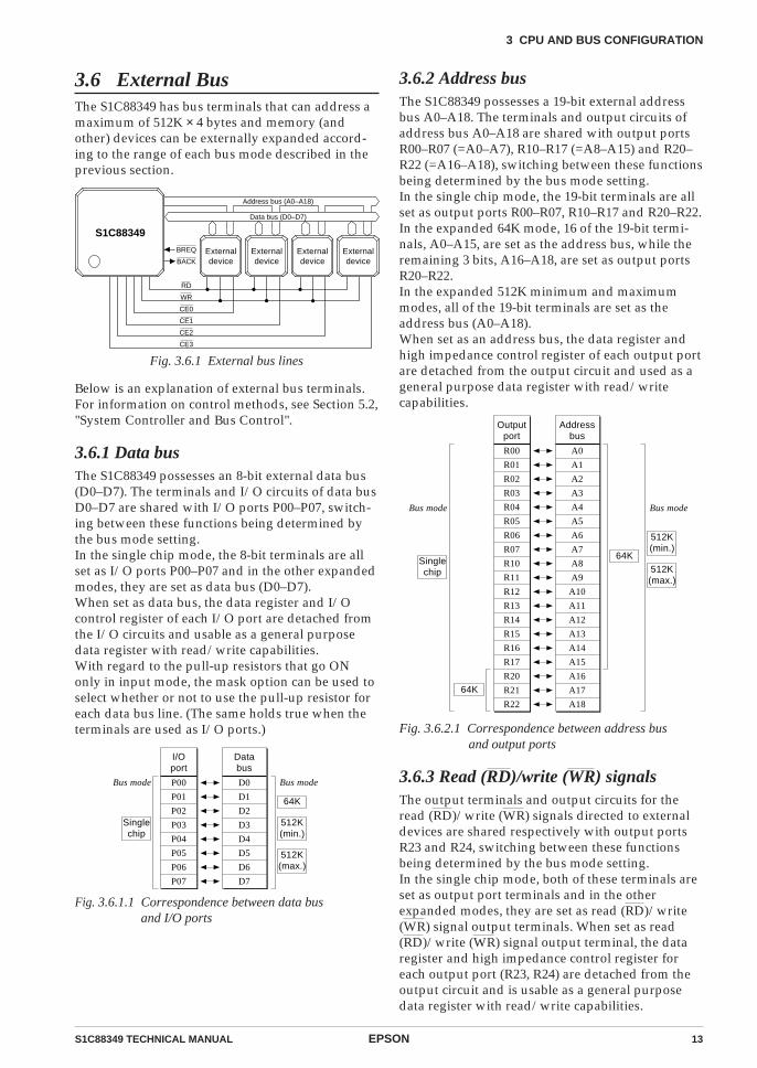
3.6 External BusThe S1C88349 has bus terminals that can address amaximum of 512K × 4 bytes and memory (andother) devices can be externally expanded accord-ing to the range of each bus mode described in theprevious section.
3.6.2 Address busThe S1C88349 possesses a 19-bit external addressbus A0–A18. The terminals and output circuits ofaddress bus A0–A18 are shared with output portsR00–R07 (=A0–A7), R10–R17 (=A8–A15) and R20–R22 (=A16–A18), switching between these functionsbeing determined by the bus mode setting.In the single chip mode, the 19-bit terminals are allset as output ports R00–R07, R10–R17 and R20–R22.In the expanded 64K mode, 16 of the 19-bit termi-nals, A0–A15, are set as the address bus, while theremaining 3 bits, A16–A18, are set as output portsR20–R22.In the expanded 512K minimum and maximummodes, all of the 19-bit terminals are set as theaddress bus (A0–A18).When set as an address bus, the data register andhigh impedance control register of each output portare detached from the output circuit and used as ageneral purpose data register with read/writecapabilities.
S1C88349
Externaldevice
Externaldevice
Externaldevice
Externaldevice
Address bus (A0–A18)
Data bus (D0–D7)
RD
WR
CE0
CE1
CE2
CE3
BREQ
BACK
Fig. 3.6.1 External bus lines
Below is an explanation of external bus terminals.For information on control methods, see Section 5.2,"System Controller and Bus Control".
3.6.1 Data busThe S1C88349 possesses an 8-bit external data bus(D0–D7). The terminals and I/O circuits of data busD0–D7 are shared with I/O ports P00–P07, switch-ing between these functions being determined bythe bus mode setting.In the single chip mode, the 8-bit terminals are allset as I/O ports P00–P07 and in the other expandedmodes, they are set as data bus (D0–D7).When set as data bus, the data register and I/Ocontrol register of each I/O port are detached fromthe I/O circuits and usable as a general purposedata register with read/write capabilities.With regard to the pull-up resistors that go ONonly in input mode, the mask option can be used toselect whether or not to use the pull-up resistor foreach data bus line. (The same holds true when theterminals are used as I/O ports.)
I/Oport
Databus
P00
P01
P02
P03
P04
P05
P06
P07
D0
D1
D2
D3
D4
D5
D6
D7
64K
Bus mode
512K(max.)
512K(min.)
Bus mode
Singlechip
Fig. 3.6.1.1 Correspondence between data bus and I/O ports
Fig. 3.6.2.1 Correspondence between address bus and output ports
3.6.3 Read (RD)/write (WR) signalsThe output terminals and output circuits for theread (RD)/write (WR) signals directed to externaldevices are shared respectively with output portsR23 and R24, switching between these functionsbeing determined by the bus mode setting.In the single chip mode, both of these terminals areset as output port terminals and in the otherexpanded modes, they are set as read (RD)/write(WR) signal output terminals. When set as read(RD)/write (WR) signal output terminal, the dataregister and high impedance control register foreach output port (R23, R24) are detached from theoutput circuit and is usable as a general purposedata register with read/write capabilities.
Outputport
Addressbus
R00
R01
R02
R03
R04
R05
R06
R07
R10
R11
R12
R13
R14
R15
R16
R17
R20
R21
R22
A0
A1
A2
A3
A4
A5
A6
A7
A8
A9
A10
A11
A12
A13
A14
A15
A16
A17
A18
64K
Bus mode
512K(max.)
512K(min.)
64K
Bus mode
Singlechip
14 EPSON S1C88349 TECHNICAL MANUAL
3 CPU AND BUS CONFIGURATION
In the single chip mode, these terminals are set asoutput ports R30–R33.
Outputport
RD/WRsignal
R23
R24
RD
WR
64K
Bus mode
512K(max.)
512K(min.)
Bus mode
Singlechip
These two signals are only output when thememory area of the external device is beingaccessed. They are not output when internalmemory is accessed.See Section 3.6.5, "WAIT control", for the outputtiming of the signal.
Outputport
CEsignal
R30
R31
R32
R33
CE0
CE1
CE2
CE3
64K
512K(max.)
512K(min.)
Bus modeBus mode
Singlechip
Fig. 3.6.4.1 Correspondence between CE signals and output ports
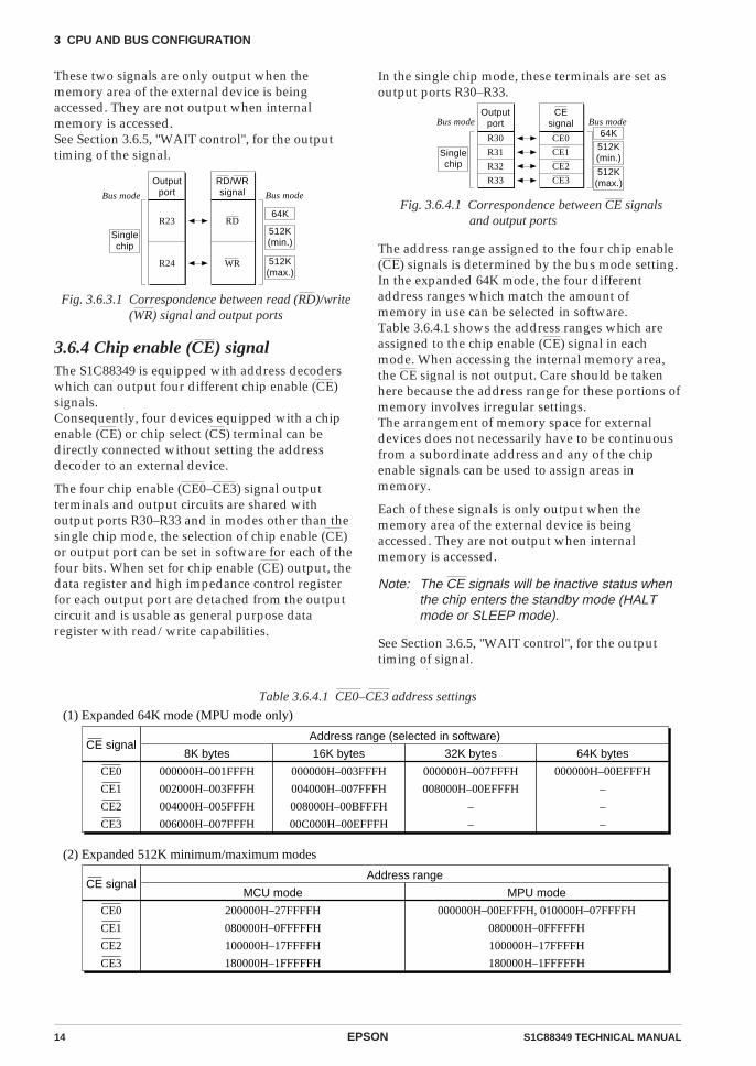
The address range assigned to the four chip enable(CE) signals is determined by the bus mode setting.In the expanded 64K mode, the four differentaddress ranges which match the amount ofmemory in use can be selected in software.Table 3.6.4.1 shows the address ranges which areassigned to the chip enable (CE) signal in eachmode. When accessing the internal memory area,the CE signal is not output. Care should be takenhere because the address range for these portions ofmemory involves irregular settings.The arrangement of memory space for externaldevices does not necessarily have to be continuousfrom a subordinate address and any of the chipenable signals can be used to assign areas inmemory.
Each of these signals is only output when thememory area of the external device is beingaccessed. They are not output when internalmemory is accessed.
Note: The CE signals will be inactive status whenthe chip enters the standby mode (HALTmode or SLEEP mode).
See Section 3.6.5, "WAIT control", for the outputtiming of signal.
Fig. 3.6.3.1 Correspondence between read (RD)/write(WR) signal and output ports
3.6.4 Chip enable (CE) signalThe S1C88349 is equipped with address decoderswhich can output four different chip enable (CE)signals.Consequently, four devices equipped with a chipenable (CE) or chip select (CS) terminal can bedirectly connected without setting the addressdecoder to an external device.
The four chip enable (CE0–CE3) signal outputterminals and output circuits are shared withoutput ports R30–R33 and in modes other than thesingle chip mode, the selection of chip enable (CE)or output port can be set in software for each of thefour bits. When set for chip enable (CE) output, thedata register and high impedance control registerfor each output port are detached from the outputcircuit and is usable as general purpose dataregister with read/write capabilities.
Table 3.6.4.1 CE0–CE3 address settings
CE0
CE1
CE2
CE3
000000H–001FFFH
002000H–003FFFH
004000H–005FFFH
006000H–007FFFH
000000H–003FFFH
004000H–007FFFH
008000H–00BFFFH
00C000H–00EFFFH
000000H–007FFFH
008000H–00EFFFH
–
–
000000H–00EFFFH
–
–
–
8K bytes 16K bytes 32K bytes 64K bytes
Address range (selected in software)CE signal
(1) Expanded 64K mode (MPU mode only)
CE0
CE1
CE2
CE3
200000H–27FFFFH
080000H–0FFFFFH
100000H–17FFFFH
180000H–1FFFFFH
000000H–00EFFFH, 010000H–07FFFFH
080000H–0FFFFFH
100000H–17FFFFH
180000H–1FFFFFH
Address rangeCE signal
(2) Expanded 512K minimum/maximum modes
MCU mode MPU mode
S1C88349 TECHNICAL MANUAL EPSON 15
3 CPU AND BUS CONFIGURATION
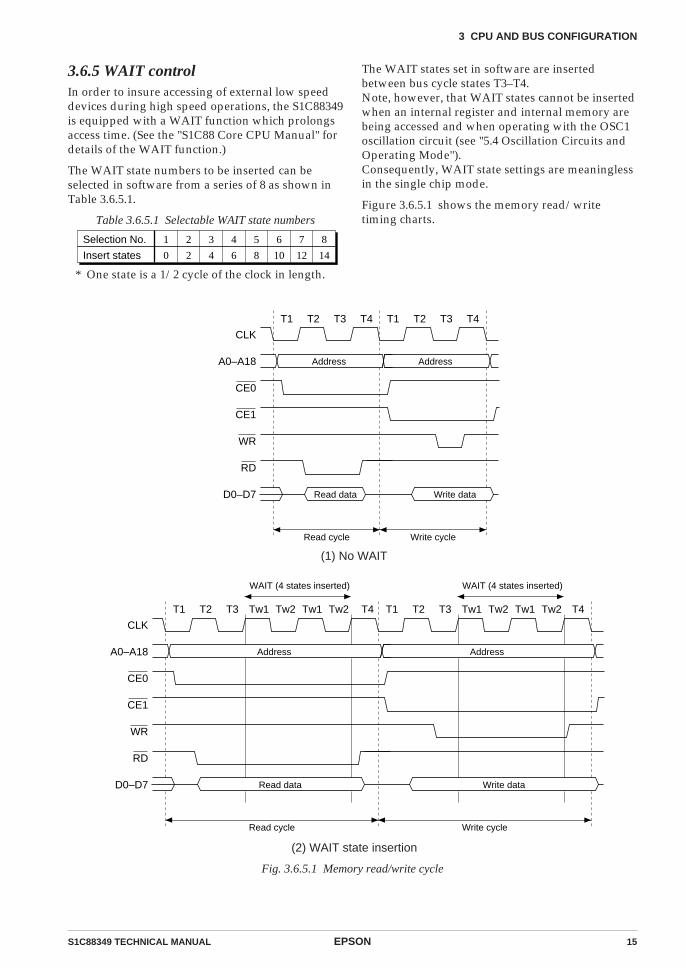
3.6.5 WAIT controlIn order to insure accessing of external low speeddevices during high speed operations, the S1C88349is equipped with a WAIT function which prolongsaccess time. (See the "S1C88 Core CPU Manual" fordetails of the WAIT function.)
The WAIT state numbers to be inserted can beselected in software from a series of 8 as shown inTable 3.6.5.1.
Table 3.6.5.1 Selectable WAIT state numbers
Selection No.
Insert states
1
0
2
2
3
4
4
6
5
8
6
10
7
12
8
14
The WAIT states set in software are insertedbetween bus cycle states T3–T4.Note, however, that WAIT states cannot be insertedwhen an internal register and internal memory arebeing accessed and when operating with the OSC1oscillation circuit (see "5.4 Oscillation Circuits andOperating Mode").Consequently, WAIT state settings are meaninglessin the single chip mode.
Figure 3.6.5.1 shows the memory read/writetiming charts.
* One state is a 1/2 cycle of the clock in length.
CLK
A0–A18
CE0
CE1
WR
RD
D0–D7
T1
Read cycle
Address
T2 T3 T4
Read data
T1
Write cycle
Address
T2 T3 T4
Write data
(1) No WAIT
CLK
A0–A18
CE0
CE1
WR
RD
D0–D7
T1
Read cycle
Address
T2 T3 T4
Read data
T1
Write cycle
Address
T2 T3 T4
Write data
Tw2 Tw2Tw1 Tw1 Tw2 Tw2Tw1 Tw1
WAIT (4 states inserted) WAIT (4 states inserted)
(2) WAIT state insertion
Fig. 3.6.5.1 Memory read/write cycle
16 EPSON S1C88349 TECHNICAL MANUAL
3 CPU AND BUS CONFIGURATION
CLK
A0–A18
D0–D7
WR
RD
BREQ
BACK
Program execution status
LD [HL],[IX]
PCHL
ANY(IX)
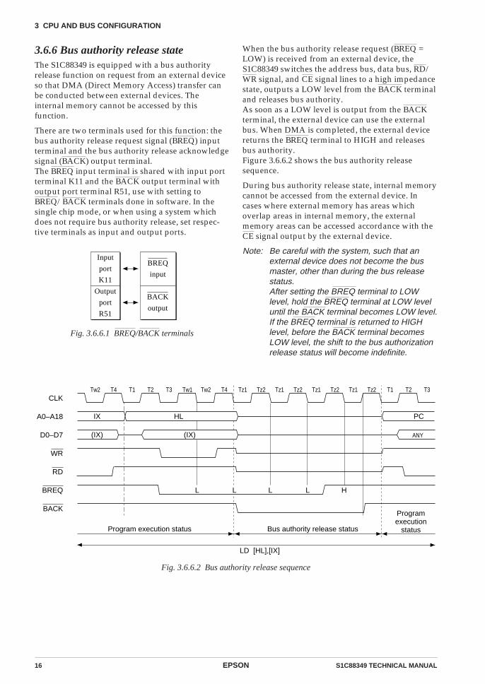
Tw2 T4 T1 T2 T3 Tw1 Tw2 T4 Tz1 Tz2 Tz1 Tz2 Tz1 Tz2 Tz1 Tz2 T1 T2 T3
IX
(IX)
Bus authority release status
Programexecution
status
L L L L H
3.6.6 Bus authority release stateThe S1C88349 is equipped with a bus authorityrelease function on request from an external deviceso that DMA (Direct Memory Access) transfer canbe conducted between external devices. Theinternal memory cannot be accessed by thisfunction.
There are two terminals used for this function: thebus authority release request signal (BREQ) inputterminal and the bus authority release acknowledgesignal (BACK) output terminal.The BREQ input terminal is shared with input portterminal K11 and the BACK output terminal withoutput port terminal R51, use with setting toBREQ/BACK terminals done in software. In thesingle chip mode, or when using a system whichdoes not require bus authority release, set respec-tive terminals as input and output ports.
Input
port
K11
Output
port
R51
BREQ
input
BACK
output
Fig. 3.6.6.1 BREQ/BACK terminals
When the bus authority release request (BREQ =LOW) is received from an external device, theS1C88349 switches the address bus, data bus, RD/WR signal, and CE signal lines to a high impedancestate, outputs a LOW level from the BACK terminaland releases bus authority.As soon as a LOW level is output from the BACKterminal, the external device can use the externalbus. When DMA is completed, the external devicereturns the BREQ terminal to HIGH and releasesbus authority.Figure 3.6.6.2 shows the bus authority releasesequence.
During bus authority release state, internal memorycannot be accessed from the external device. Incases where external memory has areas whichoverlap areas in internal memory, the externalmemory areas can be accessed accordance with theCE signal output by the external device.
Note: Be careful with the system, such that anexternal device does not become the busmaster, other than during the bus releasestatus.After setting the BREQ terminal to LOWlevel, hold the BREQ terminal at LOW leveluntil the BACK terminal becomes LOW level.If the BREQ terminal is returned to HIGHlevel, before the BACK terminal becomesLOW level, the shift to the bus authorizationrelease status will become indefinite.
Fig. 3.6.6.2 Bus authority release sequence
S1C88349 TECHNICAL MANUAL EPSON 17
4 INITIAL RESET
4 INITIAL RESETInitial reset in the S1C88349 is required in order to initialize circuits. This section of the Manual
contains a description of initial reset factors and the initial settings for internal registers, etc.
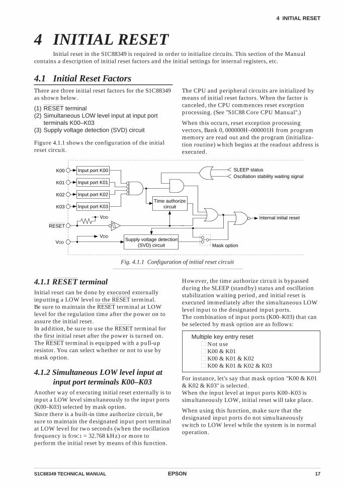
4.1 Initial Reset FactorsThere are three initial reset factors for the S1C88349as shown below.
(1) RESET terminal(2) Simultaneous LOW level input at input port
terminals K00–K03(3) Supply voltage detection (SVD) circuit
Figure 4.1.1 shows the configuration of the initialreset circuit.
The CPU and peripheral circuits are initialized bymeans of initial reset factors. When the factor iscanceled, the CPU commences reset exceptionprocessing. (See "S1C88 Core CPU Manual".)
When this occurs, reset exception processingvectors, Bank 0, 000000H–000001H from programmemory are read out and the program (initializa-tion routine) which begins at the readout address isexecuted.
K00 Input port K00
K01 Input port K01
K02 Input port K02
K03 Input port K03
VDD
RESET
VDD
VDD
SLEEP status
Time authorizecircuit
Oscillation stability waiting signal
Internal initial reset
Mask optionSupply voltage detection
(SVD) circuit
Fig. 4.1.1 Configuration of initial reset circuit
4.1.1 RESET terminalInitial reset can be done by executed externallyinputting a LOW level to the RESET terminal.Be sure to maintain the RESET terminal at LOWlevel for the regulation time after the power on toassure the initial reset.In addition, be sure to use the RESET terminal forthe first initial reset after the power is turned on.The RESET terminal is equipped with a pull-upresistor. You can select whether or not to use bymask option.
4.1.2 Simultaneous LOW level input atinput port terminals K00–K03
Another way of executing initial reset externally is toinput a LOW level simultaneously to the input ports(K00–K03) selected by mask option.Since there is a built-in time authorize circuit, besure to maintain the designated input port terminalat LOW level for two seconds (when the oscillationfrequency is fOSC1 = 32.768 kHz) or more toperform the initial reset by means of this function.
However, the time authorize circuit is bypassedduring the SLEEP (standby) status and oscillationstabilization waiting period, and initial reset isexecuted immediately after the simultaneous LOWlevel input to the designated input ports.The combination of input ports (K00–K03) that canbe selected by mask option are as follows:
Multiple key entry reset Not use K00 & K01 K00 & K01 & K02 K00 & K01 & K02 & K03
For instance, let's say that mask option "K00 & K01& K02 & K03" is selected.When the input level at input ports K00–K03 issimultaneously LOW, initial reset will take place.
When using this function, make sure that thedesignated input ports do not simultaneouslyswitch to LOW level while the system is in normaloperation.
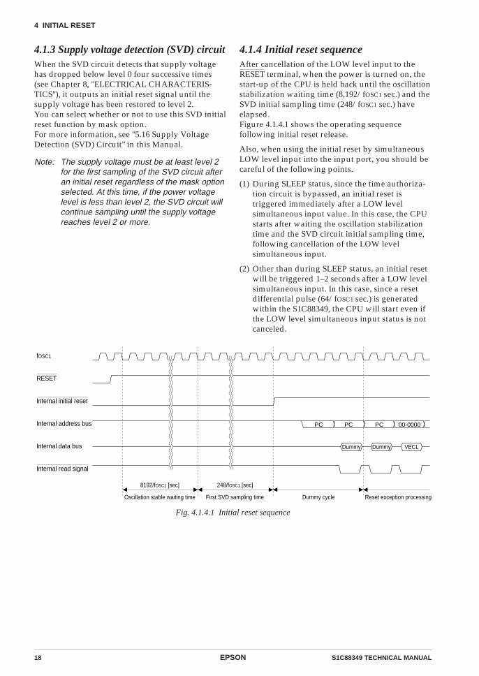
18 EPSON S1C88349 TECHNICAL MANUAL
4 INITIAL RESET
4.1.3 Supply voltage detection (SVD) circuitWhen the SVD circuit detects that supply voltagehas dropped below level 0 four successive times(see Chapter 8, "ELECTRICAL CHARACTERIS-TICS"), it outputs an initial reset signal until thesupply voltage has been restored to level 2.You can select whether or not to use this SVD initialreset function by mask option.For more information, see "5.16 Supply VoltageDetection (SVD) Circuit" in this Manual.
Note: The supply voltage must be at least level 2for the first sampling of the SVD circuit afteran initial reset regardless of the mask optionselected. At this time, if the power voltagelevel is less than level 2, the SVD circuit willcontinue sampling until the supply voltagereaches level 2 or more.
4.1.4 Initial reset sequenceAfter cancellation of the LOW level input to theRESET terminal, when the power is turned on, thestart-up of the CPU is held back until the oscillationstabilization waiting time (8,192/fOSC1 sec.) and theSVD initial sampling time (248/fOSC1 sec.) haveelapsed.Figure 4.1.4.1 shows the operating sequencefollowing initial reset release.
Also, when using the initial reset by simultaneousLOW level input into the input port, you should becareful of the following points.
(1) During SLEEP status, since the time authoriza-tion circuit is bypassed, an initial reset istriggered immediately after a LOW levelsimultaneous input value. In this case, the CPUstarts after waiting the oscillation stabilizationtime and the SVD circuit initial sampling time,following cancellation of the LOW levelsimultaneous input.
(2) Other than during SLEEP status, an initial resetwill be triggered 1–2 seconds after a LOW levelsimultaneous input. In this case, since a resetdifferential pulse (64/fOSC1 sec.) is generatedwithin the S1C88349, the CPU will start even ifthe LOW level simultaneous input status is notcanceled.
PC PC PC 00-0000
Dummy Dummy VECL
fOSC1
RESET
Internal initial reset
Internal address bus
Internal data bus
Internal read signal
8192/fOSC1 [sec]
Oscillation stable waiting time
248/fOSC1 [sec]
First SVD sampling time Dummy cycle Reset exception processing
Fig. 4.1.4.1 Initial reset sequence
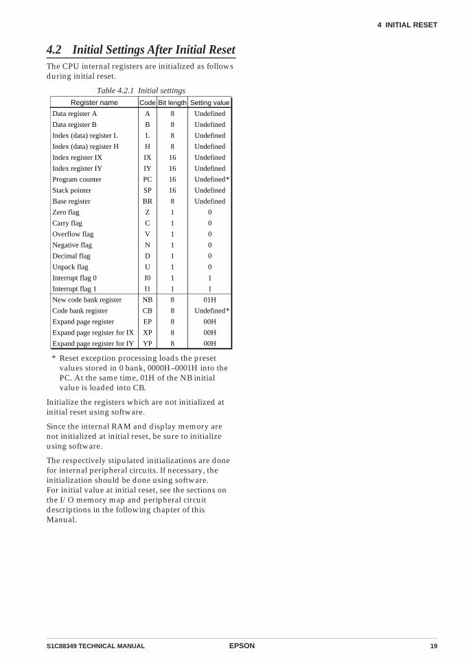
S1C88349 TECHNICAL MANUAL EPSON 19
4 INITIAL RESET
Register name Code Setting value
Data register A
Data register B
Index (data) register L
Index (data) register H
Index register IX
Index register IY
Program counter
Stack pointer
Base register
Zero flag
Carry flag
Overflow flag
Negative flag
Decimal flag
Unpack flag
Interrupt flag 0
Interrupt flag 1
New code bank register
Code bank register
Expand page register
Expand page register for IX
Expand page register for IY
A
B
L
H
IX
IY
PC
SP
BR
Z
C
V
N
D
U
I0
I1
NB
CB
EP
XP
YP
Undefined
Undefined
Undefined
Undefined
Undefined
Undefined
Undefined
Undefined
Undefined
0
0
0
0
0
0
1
1
01H
Undefined
00H
00H
00H
Bit length
8
8
8
8
16
16
16
16
8
1
1
1
1
1
1
1
1
8
8
8
8
8
*
*
4.2 Initial Settings After Initial ResetThe CPU internal registers are initialized as followsduring initial reset.
Table 4.2.1 Initial settings
* Reset exception processing loads the presetvalues stored in 0 bank, 0000H–0001H into thePC. At the same time, 01H of the NB initialvalue is loaded into CB.
Initialize the registers which are not initialized atinitial reset using software.
Since the internal RAM and display memory arenot initialized at initial reset, be sure to initializeusing software.
The respectively stipulated initializations are donefor internal peripheral circuits. If necessary, theinitialization should be done using software.For initial value at initial reset, see the sections onthe I/O memory map and peripheral circuitdescriptions in the following chapter of thisManual.
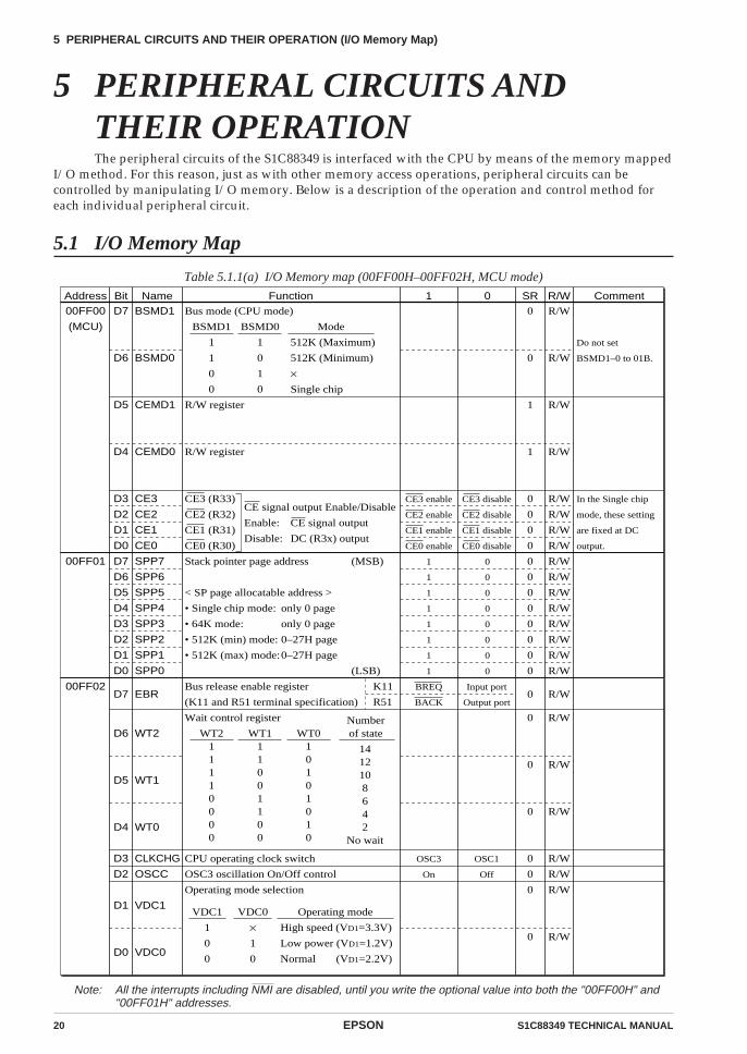
20 EPSON S1C88349 TECHNICAL MANUAL
5 PERIPHERAL CIRCUITS AND THEIR OPERATION (I/O Memory Map)
Note: All the interrupts including NMI are disabled, until you write the optional value into both the "00FF00H" and"00FF01H" addresses.
5 PERIPHERAL CIRCUITS ANDTHEIR OPERATIONThe peripheral circuits of the S1C88349 is interfaced with the CPU by means of the memory mapped
I/O method. For this reason, just as with other memory access operations, peripheral circuits can becontrolled by manipulating I/O memory. Below is a description of the operation and control method foreach individual peripheral circuit.
5.1 I/O Memory Map
Table 5.1.1(a) I/O Memory map (00FF00H–00FF02H, MCU mode)
Address Bit Name00FF00
(MCU)
D7
D6
D5
D4
D3
D2
D1
D0
BSMD1
BSMD0
CEMD1
CEMD0
CE3
CE2
CE1
CE0
SR R/WFunction CommentBus mode (CPU mode)
R/W register
R/W register
CE3 (R33)
CE2 (R32)
CE1 (R31)
CE0 (R30)
Do not set
BSMD1–0 to 01B.
In the Single chip
mode, these setting
are fixed at DC
output.
1 00
0
1
1
0
0
0
0
R/W
R/W
R/W
R/W
R/W
R/W
R/W
R/W
CE3 enable
CE2 enable
CE1 enable
CE0 enable
BSMD1
1
1
0
0
BSMD0
1
0
1
0
Mode
512K (Maximum)
512K (Minimum)
×Single chip
CE signal output
DC (R3x) output
CE signal output Enable/Disable
Enable:
Disable:
CE3 disable
CE2 disable
CE1 disable
CE0 disable
00FF01 D7
D6
D5
D4
D3
D2
D1
D0
SPP7
SPP6
SPP5
SPP4
SPP3
SPP2
SPP1
SPP0
Stack pointer page address
< SP page allocatable address >
• Single chip mode:
• 64K mode:
• 512K (min) mode:
• 512K (max) mode:
0
0
0
0
0
0
0
0
R/W
R/W
R/W
R/W
R/W
R/W
R/W
R/W
1
1
1
1
1
1
1
1
0
0
0
0
0
0
0
0
(MSB)
(LSB)
only 0 page
only 0 page
0–27H page
0–27H page
00FF02D7
D6
D5
D4
D3
D2
D1
D0
EBR
WT2
WT1
WT0
CLKCHG
OSCC
VDC1
VDC0
Bus release enable register
(K11 and R51 terminal specification)
Wait control register
CPU operating clock switch
OSC3 oscillation On/Off control
Operating mode selection
0
0
0
0
0
0
0
0
R/W
R/W
R/W
R/W
R/W
R/W
R/W
R/W
BREQ
BACK
OSC3
On
WT211110000
WT111001100
Numberof state
1412108642
No wait
Input port
Output port
OSC1
Off
K11
R51
VDC1
1
0
0
VDC0
×1
0
High speed (VD1=3.3V)
Low power (VD1=1.2V)
Normal (VD1=2.2V)
WT010101010
Operating mode
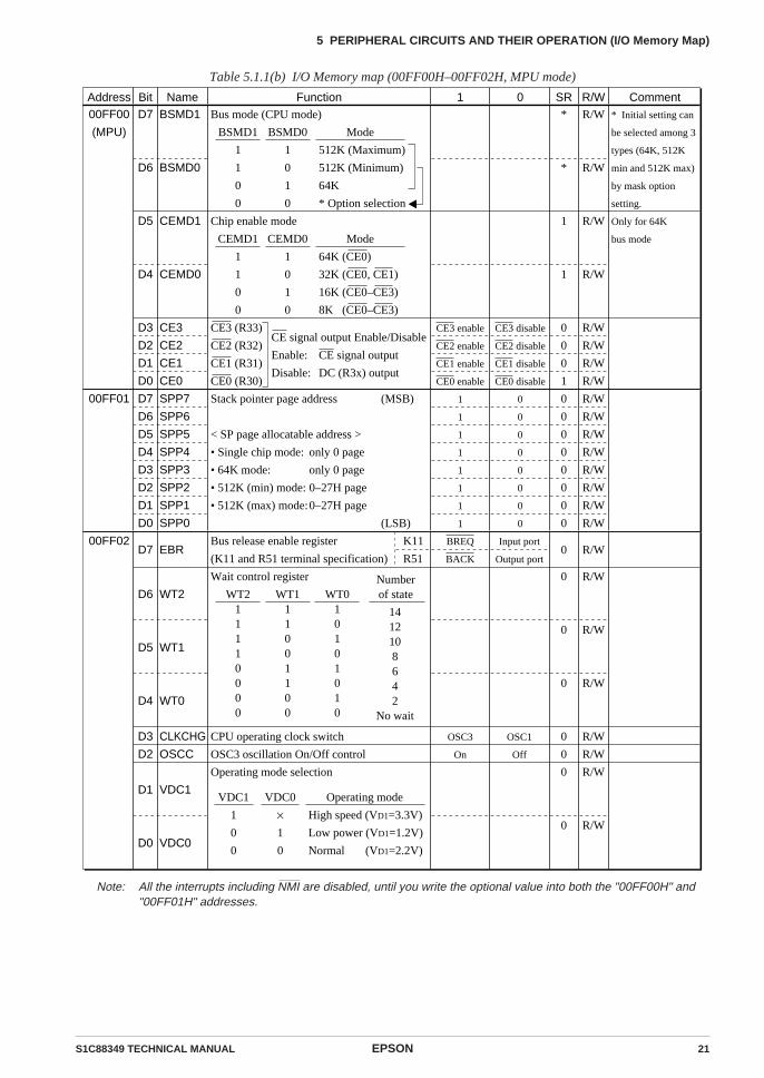
S1C88349 TECHNICAL MANUAL EPSON 21
5 PERIPHERAL CIRCUITS AND THEIR OPERATION (I/O Memory Map)
Table 5.1.1(b) I/O Memory map (00FF00H–00FF02H, MPU mode)
Note: All the interrupts including NMI are disabled, until you write the optional value into both the "00FF00H" and"00FF01H" addresses.
Address Bit Name SR R/WFunction Comment1 000FF00
(MPU)
D7
D6
D5
D4
D3
D2
D1
D0
BSMD1
BSMD0
CEMD1
CEMD0
CE3
CE2
CE1
CE0
Bus mode (CPU mode)
Chip enable mode
CE3 (R33)
CE2 (R32)
CE1 (R31)
CE0 (R30)
R/W
R/W
R/W
R/W
R/W
R/W
R/W
R/W
CE3 enable
CE2 enable
CE1 enable
CE0 enable
CE3 disable
CE2 disable
CE1 disable
CE0 disable
BSMD1
1
1
0
0
BSMD0
1
0
1
0
Mode
CE signal output
DC (R3x) output
CE signal output Enable/Disable
Enable:
Disable:
00FF01 D7
D6
D5
D4
D3
D2
D1
D0
SPP7
SPP6
SPP5
SPP4
SPP3
SPP2
SPP1
SPP0
Stack pointer page address
< SP page allocatable address >
• Single chip mode:
• 64K mode:
• 512K (min) mode:
• 512K (max) mode:
0
0
0
0
0
0
0
0
R/W
R/W
R/W
R/W
R/W
R/W
R/W
R/W
1
1
1
1
1
1
1
1
0
0
0
0
0
0
0
0
(MSB)
(LSB)
only 0 page
only 0 page
0–27H page
0–27H page
00FF02D7
D6
D5
D4
D3
D2
D1
D0
EBR
WT2
WT1
WT0
CLKCHG
OSCC
VDC1
VDC0
Bus release enable register
(K11 and R51 terminal specification)
Wait control register
CPU operating clock switch
OSC3 oscillation On/Off control
Operating mode selection
BREQ
BACK
OSC3
On
WT211110000
WT111001100
Numberof state
1412108642
No wait
Input port
Output port
OSC1
Off
K11
R51
VDC1
1
0
0
VDC0
×1
0
Operating mode
WT010101010
CEMD1
1
1
0
0
CEMD0
1
0
1
0
Mode
64K (CE0)
32K (CE0, CE1)
16K (CE0–CE3)
8K (CE0–CE3)
0
0
0
0
0
0
0
0
R/W
R/W
R/W
R/W
R/W
R/W
R/W
R/WHigh speed (VD1=3.3V)
Low power (VD1=1.2V)
Normal (VD1=2.2V)
* Initial setting can
be selected among 3
types (64K, 512K
min and 512K max)
by mask option
setting.
Only for 64K
bus mode
*
*
1
1
0
0
0
1
512K (Maximum)
512K (Minimum)
64K
* Option selection
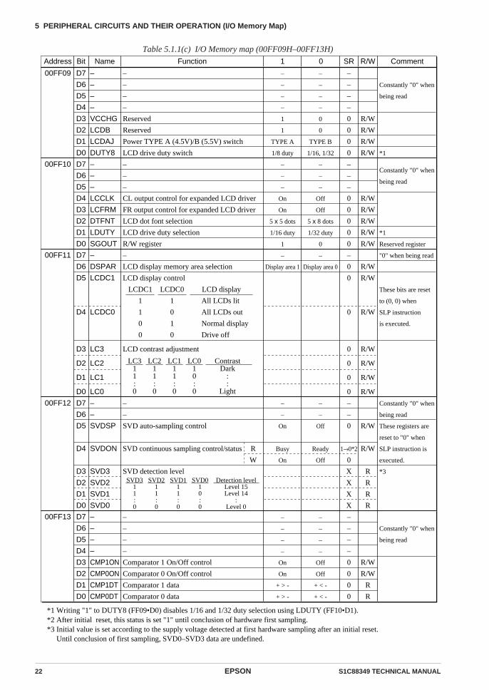
22 EPSON S1C88349 TECHNICAL MANUAL
5 PERIPHERAL CIRCUITS AND THEIR OPERATION (I/O Memory Map)
Table 5.1.1(c) I/O Memory map (00FF09H–00FF13H)
Address Bit Name
00FF10 D7
D6
D5
D4
D3
D2
D1
D0
–
–
–
LCCLK
LCFRM
DTFNT
LDUTY
SGOUT
SR R/WFunction Comment
–
–
–
CL output control for expanded LCD driver
FR output control for expanded LCD driver
LCD dot font selection
LCD drive duty selection
R/W register
Constantly "0" when
being read
1 0
–
–
–
0
0
0
0
0
R/W
R/W
R/W
R/W
R/W
–
–
–
On
On
5 x 5 dots
1/16 duty
1
–
–
–
Off
Off
5 x 8 dots
1/32 duty
0
00FF11 D7
D6
D5
D4
D3
D2
D1
D0
–
DSPAR
LCDC1
LCDC0
LC3
LC2
LC1
LC0
–
LCD display memory area selection
LCD display control
LCD contrast adjustment
"0" when being read
These bits are reset
to (0, 0) when
SLP instruction
is executed.
–
0
0
0
0
0
0
0
R/W
R/W
R/W
R/W
R/W
R/W
R/W
–
Display area 1
–
Display area 0
LCDC1
1
1
0
0
LCDC0
1
0
1
0
LCD display
All LCDs lit
All LCDs out
Normal display
Drive off
LC311:0
LC211:0
LC111:0
LC010:0
ContrastDark
::
Light
*1
Reserved register
00FF09 D7
D6
D5
D4
D3
D2
D1
D0
–
–
–
–
VCCHG
LCDB
LCDAJ
DUTY8
–
–
–
–
Reserved
Reserved
Power TYPE A (4.5V)/B (5.5V) switch
LCD drive duty switch
Constantly "0" when
being read
–
–
–
–
0
0
0
0
R/W
R/W
R/W
R/W
–
–
–
–
1
1
TYPE A
1/8 duty
–
–
–
–
0
0
TYPE B
1/16, 1/32 *1
00FF12 D7
D6
D5
D4
D3
D2
D1
D0
–
–
SVDSP
SVDON
SVD3
SVD2
SVD1
SVD0
–
–
SVD auto-sampling control
SVD continuous sampling control/status
SVD detection level
Constantly "0" when
being read
These registers are
reset to "0" when
SLP instruction is
executed.
*3
–
–
0
1→0*2
0
X
X
X
X
R/W
R/W
R
R
R
R
–
–
On
Busy
On
–
–
Off
Ready
Off
R
W
SVD311:0
SVD211:0
SVD111:0
SVD010:0
Detection levelLevel 15Level 14
:Level 0
*1 Writing "1" to DUTY8 (FF09•D0) disables 1/16 and 1/32 duty selection using LDUTY (FF10•D1).*2 After initial reset, this status is set "1" until conclusion of hardware first sampling.*3 Initial value is set according to the supply voltage detected at first hardware sampling after an initial reset. Until conclusion of first sampling, SVD0–SVD3 data are undefined.
00FF13 D7
D6
D5
D4
D3
D2
D1
D0
–
–
–
–
CMP1ON
CMP0ON
CMP1DT
CMP0DT
–
–
–
–
Comparator 1 On/Off control
Comparator 0 On/Off control
Comparator 1 data
Comparator 0 data
Constantly "0" when
being read
–
–
–
–
0
0
0
0
R/W
R/W
R
R
–
–
–
–
On
On
+ > -
+ > -
–
–
–
–
Off
Off
+ < -
+ < -
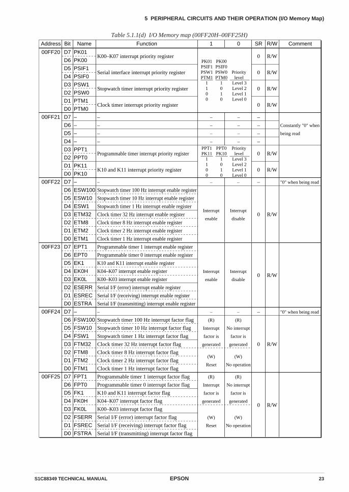
S1C88349 TECHNICAL MANUAL EPSON 23
5 PERIPHERAL CIRCUITS AND THEIR OPERATION (I/O Memory Map)
Table 5.1.1(d) I/O Memory map (00FF20H–00FF25H)
Address Bit Name SR R/WFunction Comment1 0
00FF20 D7
D6
D5
D4
D3
D2
D1
D0
PK01
PK00
PSIF1
PSIF0
PSW1
PSW0
PTM1
PTM0
K00–K07 interrupt priority register
Serial interface interrupt priority register
Stopwatch timer interrupt priority register
Clock timer interrupt priority register
0
0
0
0
R/W
R/W
R/W
R/W
PK01PSIF1PSW1PTM1
1100
PK00PSIF0PSW0PTM0
1010
Prioritylevel
Level 3Level 2Level 1Level 0
00FF21 D7
D6
D5
D4
D3
D2
D1
D0
–
–
–
–
PPT1
PPT0
PK11
PK10
–
–
–
–
Programmable timer interrupt priority register
K10 and K11 interrupt priority register
Constantly "0" when
being read
–
–
–
–
0
0
R/W
R/W
–
–
–
–
–
–
–
–PPT1PK11
1100
PPT0PK10
1010
Prioritylevel
Level 3Level 2Level 1Level 0
00FF22 D7
D6
D5
D4
D3
D2
D1
D0
–
ESW100
ESW10
ESW1
ETM32
ETM8
ETM2
ETM1
–
Stopwatch timer 100 Hz interrupt enable register
Stopwatch timer 10 Hz interrupt enable register
Stopwatch timer 1 Hz interrupt enable register
Clock timer 32 Hz interrupt enable register
Clock timer 8 Hz interrupt enable register
Clock timer 2 Hz interrupt enable register
Clock timer 1 Hz interrupt enable register
"0" when being read–
0 R/W
–
Interrupt
enable
–
Interrupt
disable
D7
D6
D5
D4
D3
D2
D1
D0
00FF24 D7
D6
D5
D4
D3
D2
D1
D0
–
FSW100
FSW10
FSW1
FTM32
FTM8
FTM2
FTM1
–
Stopwatch timer 100 Hz interrupt factor flag
Stopwatch timer 10 Hz interrupt factor flag
Stopwatch timer 1 Hz interrupt factor flag
Clock timer 32 Hz interrupt factor flag
Clock timer 8 Hz interrupt factor flag
Clock timer 2 Hz interrupt factor flag
Clock timer 1 Hz interrupt factor flag
"0" when being read–
0 R/W
–
(R)
Interrupt
factor is
generated
(W)
Reset
–
(R)
No interrupt
factor is
generated
(W)
No operation
00FF25 D7
D6
D5
D4
D3
D2
D1
D0
FPT1
FPT0
FK1
FK0H
FK0L
FSERR
FSREC
FSTRA
Programmable timer 1 interrupt factor flag
Programmable timer 0 interrupt factor flag
K10 and K11 interrupt factor flag
K04–K07 interrupt factor flag
K00–K03 interrupt factor flag
Serial I/F (error) interrupt factor flag
Serial I/F (receiving) interrupt factor flag
Serial I/F (transmitting) interrupt factor flag
0 R/W
(R)
Interrupt
factor is
generated
(W)
Reset
(R)
No interrupt
factor is
generated
(W)
No operation
00FF23 EPT1
EPT0
EK1
EK0H
EK0L
ESERR
ESREC
ESTRA
Programmable timer 1 interrupt enable register
Programmable timer 0 interrupt enable register
K10 and K11 interrupt enable register
K04–K07 interrupt enable register
K00–K03 interrupt enable register
Serial I/F (error) interrupt enable register
Serial I/F (receiving) interrupt enable register
Serial I/F (transmitting) interrupt enable register
0 R/WInterrupt
enable
Interrupt
disable
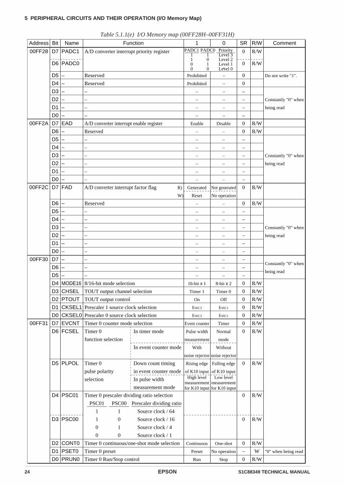
24 EPSON S1C88349 TECHNICAL MANUAL
5 PERIPHERAL CIRCUITS AND THEIR OPERATION (I/O Memory Map)
Table 5.1.1(e) I/O Memory map (00FF28H–00FF31H)
Address Bit Name
00FF30 D7
D6
D5
D4
D3
D2
D1
D0
–
–
–
MODE16
CHSEL
PTOUT
CKSEL1
CKSEL0
SR R/WFunction Comment
–
–
–
8/16-bit mode selection
TOUT output channel selection
TOUT output control
Prescaler 1 source clock selection
Prescaler 0 source clock selection
Constantly "0" when
being read
1 0
–
–
–
0
0
0
0
0
R/W
R/W
R/W
R/W
R/W
–
–
–
16-bit x 1
Timer 1
On
fOSC3
fOSC3
–
–
–
8-bit x 2
Timer 0
Off
fOSC1
fOSC1
00FF31 D7
D6
D5
D4
D3
D2
D1
D0
EVCNT
FCSEL
PLPOL
PSC01
PSC00
CONT0
PSET0
PRUN0
Timer 0 counter mode selection
Timer 0
function selection
Timer 0
pulse polarity
selection
Timer 0 prescaler dividing ratio selection
Timer 0 continuous/one-shot mode selection
Timer 0 preset
Timer 0 Run/Stop control
"0" when being read
0
0
0
0
0
0
–
0
R/W
R/W
R/W
R/W
R/W
R/W
W
R/W
Timer
Normal
mode
Without
noise rejector
Falling edge
of K10 inputLow level
measurementfor K10 input
One-shot
No operation
Stop
In timer mode
In event counter mode
Down count timing
in event counter mode
In pulse width
measurement mode
PSC01
1
1
0
0
PSC00
1
0
1
0
Prescaler dividing ratio
Source clock / 64
Source clock / 16
Source clock / 4
Source clock / 1
00FF28 D7
D6
D5
D4
D3
D2
D1
D0
PADC1
PADC0
–
–
–
–
–
–
A/D converter interrupt priority register
Reserved
Reserved
–
–
–
–
Do not write "1".
Constantly "0" when
being read
0
0
0
0
–
–
–
–
R/W
R/W
Prohibited
Prohibited
–
–
–
–
–
–
–
–
–
–
–
PADC11100
PADC01010
PriorityLevel 3Level 2Level 1Level 0
00FF2A D7
D6
D5
D4
D3
D2
D1
D0
EAD
–
–
–
–
–
–
–
A/D converter interrupt enable register
Reserved
–
–
–
–
–
–
Constantly "0" when
being read
0
0
–
–
–
–
–
–
R/W
R/W
Enable
–
–
–
–
–
–
–
Disable
–
–
–
–
–
–
–
00FF2C D7
D6
D5
D4
D3
D2
D1
D0
FAD
–
–
–
–
–
–
–
A/D converter interrupt factor flag
Reserved
–
–
–
–
–
–
Constantly "0" when
being read
0
0
–
–
–
–
–
–
R/W
R/W
Generated
Reset
R)
W)
Not generated
No operation
–
–
–
–
–
–
–
–
–
–
–
–
–
–
Event counter
Pulse width
measurement
With
noise rejector
Rising edge
of K10 inputHigh level
measurementfor K10 input
Continuous
Preset
Run

S1C88349 TECHNICAL MANUAL EPSON 25
5 PERIPHERAL CIRCUITS AND THEIR OPERATION (I/O Memory Map)
Table 5.1.1(f) I/O Memory map (00FF32H–00FF36H)
Address Bit Name SR R/WFunction Comment1 0
00FF32
D7
D6
D5
D4
D3
D2
D1
D0
RLD07
RLD06
RLD05
RLD04
RLD03
RLD02
RLD01
RLD00
Timer 0 reload data D7 (MSB)
Timer 0 reload data D6
Timer 0 reload data D5
Timer 0 reload data D4
Timer 0 reload data D3
Timer 0 reload data D2
Timer 0 reload data D1
Timer 0 reload data D0 (LSB)
1 R/WHigh Low
00FF33
D7
D6
D5
D4
D3
D2
D1
D0
–
–
–
PSC11
PSC10
CONT1
PSET1
PRUN1
–
–
–
Timer 1 prescaler dividing ratio selection
Timer 1 continuous/one-shot mode selection
Timer 1 preset
Timer 1 Run/Stop control
Constantly "0" when
being read
"0" when being read
–
–
–
0
0
0
–
0
R/W
R/W
R/W
W
R/W
–
–
–
Continuous
Preset
Run
–
–
–
One-shot
No operation
Stop
PSC11
1
1
0
0
PSC10
1
0
1
0
Prescaler dividing ratio
Source clock / 64
Source clock / 16
Source clock / 4
Source clock / 1
D7
D6
D5
D4
D3
D2
D1
D0
RLD17
RLD16
RLD15
RLD14
RLD13
RLD12
RLD11
RLD10
Timer 1 reload data D7 (MSB)
Timer 1 reload data D6
Timer 1 reload data D5
Timer 1 reload data D4
Timer 1 reload data D3
Timer 1 reload data D2
Timer 1 reload data D1
Timer 1 reload data D0 (LSB)
1 R/WHigh Low
00FF34
D7
D6
D5
D4
D3
D2
D1
D0
PTD07
PTD06
PTD05
PTD04
PTD03
PTD02
PTD01
PTD00
Timer 0 counter data D7 (MSB)
Timer 0 counter data D6
Timer 0 counter data D5
Timer 0 counter data D4
Timer 0 counter data D3
Timer 0 counter data D2
Timer 0 counter data D1
Timer 0 counter data D0 (LSB)
1 RHigh Low
00FF35
D7
D6
D5
D4
D3
D2
D1
D0
PTD17
PTD16
PTD15
PTD14
PTD13
PTD12
PTD11
PTD10
Timer 1 counter data D7 (MSB)
Timer 1 counter data D6
Timer 1 counter data D5
Timer 1 counter data D4
Timer 1 counter data D3
Timer 1 counter data D2
Timer 1 counter data D1
Timer 1 counter data D0 (LSB)
1 RHigh Low
00FF36
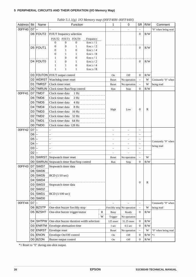
26 EPSON S1C88349 TECHNICAL MANUAL
5 PERIPHERAL CIRCUITS AND THEIR OPERATION (I/O Memory Map)
Table 5.1.1(g) I/O Memory map (00FF40H–00FF44H)
Address Bit Name
00FF40 D7
D6
D5
D4
D3
D2
D1
D0
–
FOUT2
FOUT1
FOUT0
FOUTON
WDRST
TMRST
TMRUN
SR R/WFunction Comment
–
FOUT frequency selection
FOUT output control
Watchdog timer reset
Clock timer reset
Clock timer Run/Stop control
"0" when being read
Constantly "0" when
being read
1 0
–
0
0
0
0
–
–
0
R/W
R/W
R/W
R/W
W
W
R/W
–
On
Reset
Reset
Run
–
Off
No operation
No operation
Stop
00FF41 D7
D6
D5
D4
D3
D2
D1
D0
TMD7
TMD6
TMD5
TMD4
TMD3
TMD2
TMD1
TMD0
Clock timer data
Clock timer data
Clock timer data
Clock timer data
Clock timer data
Clock timer data
Clock timer data
Clock timer data
0 RHigh Low
1 Hz
2 Hz
4 Hz
8 Hz
16 Hz
32 Hz
64 Hz
128 Hz
FOUT2
00001111
FOUT1
00110011
FOUT0
01010101
Frequency
fOSC1 / 1fOSC1 / 2fOSC1 / 4fOSC1 / 8fOSC3 / 1fOSC3 / 2fOSC3 / 4fOSC3 / 8
00FF42 D7
D6
D5
D4
D3
D2
D1
D0
–
–
–
–
–
–
SWRST
SWRUN
–
–
–
–
–
–
Stopwatch timer reset
Stopwatch timer Run/Stop control
Constantly "0" when
being read
–
–
–
–
–
–
–
0
W
R/W
–
–
–
–
–
–
Reset
Run
–
–
–
–
–
–
No operation
Stop
00FF43 D7
D6
D5
D4
D3
D2
D1
D0
SWD7
SWD6
SWD5
SWD4
SWD3
SWD2
SWD1
SWD0
Stopwatch timer data
BCD (1/10 sec)
Stopwatch timer data
BCD (1/100 sec)
0 R
00FF44 D7
D6
D5
D4
D3
D2
D1
D0
–
BZSTP
BZSHT
SHTPW
ENRTM
ENRST
ENON
BZON
–
One-shot buzzer forcibly stop
One-shot buzzer trigger/status
One-shot buzzer duration width selection
Envelope attenuation time
Envelope reset
Envelope On/Off control
Buzzer output control
Constantly "0" when
being read
"0" when being read
*1
–
–
0
0
0
–
0
0
W
R/W
R/W
R/W
W
R/W
R/W
–
Forcibly stop
Busy
Trigger
125 msec
1 sec
Reset
On
On
–
No operation
Ready
No operation
31.25 msec
0.5 sec
No operation
Off
Off
R
W
*1 Reset to "0" during one-shot output.
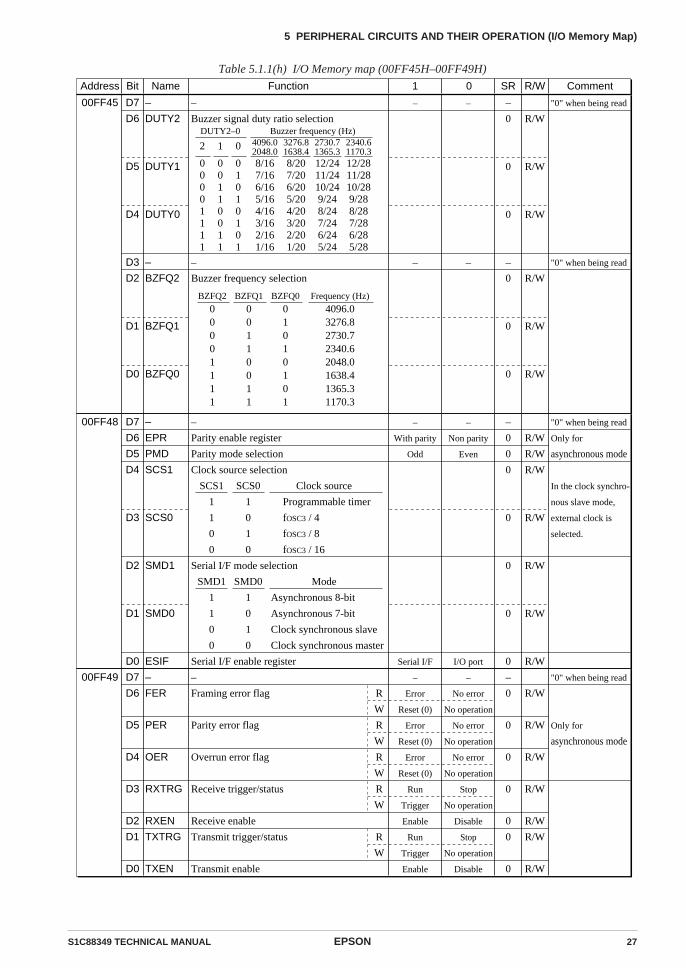
S1C88349 TECHNICAL MANUAL EPSON 27
5 PERIPHERAL CIRCUITS AND THEIR OPERATION (I/O Memory Map)
Table 5.1.1(h) I/O Memory map (00FF45H–00FF49H)
Address Bit Name SR R/WFunction Comment1 0
00FF45 D7
D6
D5
D4
D3
D2
D1
D0
–
DUTY2
DUTY1
DUTY0
–
BZFQ2
BZFQ1
BZFQ0
–
Buzzer signal duty ratio selection
–
Buzzer frequency selection
"0" when being read
"0" when being read
–
0
0
0
–
0
0
0
R/W
R/W
R/W
R/W
R/W
R/W
–
–
–
–
00001111
00110011
01010101
8/167/166/165/164/163/162/161/16
4096.02048.0
8/207/206/205/204/203/202/201/20
3276.81638.4
12/2411/2410/249/248/247/246/245/24
2730.71365.3
12/2811/2810/289/288/287/286/285/28
2340.61170.3
2 1 0
Buzzer frequency (Hz)DUTY2–0
BZFQ2
00001111
BZFQ1
00110011
BZFQ0
01010101
Frequency (Hz)
4096.03276.82730.72340.62048.01638.41365.31170.3
00FF48 D7
D6
D5
D4
D3
D2
D1
D0
–
EPR
PMD
SCS1
SCS0
SMD1
SMD0
ESIF
–
Parity enable register
Parity mode selection
Clock source selection
Serial I/F mode selection
Serial I/F enable register
"0" when being read
Only for
asynchronous mode
In the clock synchro-
nous slave mode,
external clock is
selected.
–
0
0
0
0
0
0
0
R/W
R/W
R/W
R/W
R/W
R/W
R/W
–
With parity
Odd
Serial I/F
–
Non parity
Even
I/O port
SCS1
1
1
0
0
SCS0
1
0
1
0
Clock source
Programmable timer
fOSC3 / 4
fOSC3 / 8
fOSC3 / 16
SMD1
1
1
0
0
SMD0
1
0
1
0
Mode
Asynchronous 8-bit
Asynchronous 7-bit
Clock synchronous slave
Clock synchronous master
00FF49 D7
D6
D5
D4
D3
D2
D1
D0
–
FER
PER
OER
RXTRG
RXEN
TXTRG
TXEN
–
Framing error flag
Parity error flag
Overrun error flag
Receive trigger/status
Receive enable
Transmit trigger/status
Transmit enable
"0" when being read
Only for
asynchronous mode
–
0
0
0
0
0
0
0
R/W
R/W
R/W
R/W
R/W
R/W
R/W
–
No error
No operation
No error
No operation
No error
No operation
Stop
No operation
Disable
Stop
No operation
Disable
R
W
R
W
R
W
R
W
R
W
–
Error
Reset (0)
Error
Reset (0)
Error
Reset (0)
Run
Trigger
Enable
Run
Trigger
Enable

28 EPSON S1C88349 TECHNICAL MANUAL
5 PERIPHERAL CIRCUITS AND THEIR OPERATION (I/O Memory Map)
Table 5.1.1(i) I/O Memory map (00FF4AH–00FF54H)
Address Bit Name SR R/WFunction Comment1 0
00FF4A D7
D6
D5
D4
D3
D2
D1
D0
TRXD7
TRXD6
TRXD5
TRXD4
TRXD3
TRXD2
TRXD1
TRXD0
X R/WHigh Low
Transmit/Receive data D7 (MSB)
Transmit/Receive data D6
Transmit/Receive data D5
Transmit/Receive data D4
Transmit/Receive data D3
Transmit/Receive data D2
Transmit/Receive data D1
Transmit/Receive data D0 (LSB)
00FF50 D7
D6
D5
D4
D3
D2
D1
D0
SIK07
SIK06
SIK05
SIK04
SIK03
SIK02
SIK01
SIK00
K07 interrupt selection register
K06 interrupt selection register
K05 interrupt selection register
K04 interrupt selection register
K03 interrupt selection register
K02 interrupt selection register
K01 interrupt selection register
K00 interrupt selection register
0 R/WInterrupt
enable
Interrupt
disable
00FF51 D7
D6
D5
D4
D3
D2
D1
D0
–
–
–
–
–
–
SIK11
SIK10
–
–
–
–
–
–
K11 interrupt selection register
K10 interrupt selection register
Constantly "0" when
being read
–
–
–
–
–
–
0 R/W
–
–
–
–
–
–
Interrupt
enable
–
–
–
–
–
–
Interrupt
disable
00FF53 D7
D6
D5
D4
D3
D2
D1
D0
–
–
–
–
–
–
KCP11
KCP10
–
–
–
–
–
–
K11 interrupt comparison register
K10 interrupt comparison register
Constantly "0" when
being read
–
–
–
–
–
–
1 R/W
–
–
–
–
–
–
Falling
edge
–
–
–
–
–
–
Rising
edge
00FF52 D7
D6
D5
D4
D3
D2
D1
D0
KCP07
KCP06
KCP05
KCP04
KCP03
KCP02
KCP01
KCP00
K07 interrupt comparison register
K06 interrupt comparison register
K05 interrupt comparison register
K04 interrupt comparison register
K03 interrupt comparison register
K02 interrupt comparison register
K01 interrupt comparison register
K00 interrupt comparison register
1 R/W
Interrupt
generated
at falling
edge
Interrupt
generated
at rising
edge
00FF54 D7
D6
D5
D4
D3
D2
D1
D0
K07D
K06D
K05D
K04D
K03D
K02D
K01D
K00D
K07 input port data
K06 input port data
K05 input port data
K04 input port data
K03 input port data
K02 input port data
K01 input port data
K00 input port data
– RHigh level
input
Low level
input
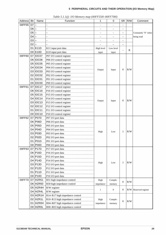
S1C88349 TECHNICAL MANUAL EPSON 29
5 PERIPHERAL CIRCUITS AND THEIR OPERATION (I/O Memory Map)
Table 5.1.1(j) I/O Memory map (00FF55H–00FF70H)
Address Bit Name SR R/WFunction Comment1 0
00FF55 D7
D6
D5
D4
D3
D2
D1
D0
–
–
–
–
–
–
K11D
K10D
–
–
–
–
–
–
K11 input port data
K10 input port data
Constantly "0" when
being read
–
–
–
–
–
–
– R
–
–
–
–
–
–
High level
input
–
–
–
–
–
–
Low level
input
00FF61 D7
D6
D5
D4
D3
D2
D1
D0
IOC17
IOC16
IOC15
IOC14
IOC13
IOC12
IOC11
IOC10
P17 I/O control register
P16 I/O control register
P15 I/O control register
P14 I/O control register
P13 I/O control register
P12 I/O control register
P11 I/O control register
P10 I/O control register
0 R/WOutput Input
00FF62 D7
D6
D5
D4
D3
D2
D1
D0
P07D
P06D
P05D
P04D
P03D
P02D
P01D
P00D
P07 I/O port data
P06 I/O port data
P05 I/O port data
P04 I/O port data
P03 I/O port data
P02 I/O port data
P01 I/O port data
P00 I/O port data
1 R/WHigh Low
00FF63 D7
D6
D5
D4
D3
D2
D1
D0
P17D
P16D
P15D
P14D
P13D
P12D
P11D
P10D
P17 I/O port data
P16 I/O port data
P15 I/O port data
P14 I/O port data
P13 I/O port data
P12 I/O port data
P11 I/O port data
P10 I/O port data
1 R/WHigh Low
00FF60 D7
D6
D5
D4
D3
D2
D1
D0
IOC07
IOC06
IOC05
IOC04
IOC03
IOC02
IOC01
IOC00
P07 I/O control register
P06 I/O control register
P05 I/O control register
P04 I/O control register
P03 I/O control register
P02 I/O control register
P01 I/O control register
P00 I/O control register
0 R/WOutput Input
00FF70 D7
D6
D5
D4
D3
D2
D1
D0
HZR51
HZR50
HZR4H
HZR4L
HZR1H
HZR1L
HZR0H
HZR0L
R51 high impedance control
R50 high impedance control
R/W register
R/W register
R14–R17 high impedance control
R10–R13 high impedance control
R04–R07 high impedance control
R00–R03 high impedance control
Reserved register
0
0
0
R/W
R/W
R/W
High
impedance
1
High
impedance
Comple-
mentary
0
Comple-
mentary
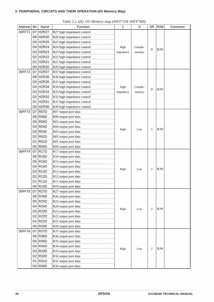
30 EPSON S1C88349 TECHNICAL MANUAL
5 PERIPHERAL CIRCUITS AND THEIR OPERATION (I/O Memory Map)
Table 5.1.1(k) I/O Memory map (00FF71H–00FF76H)
Address Bit Name SR R/WFunction Comment1 0
00FF71 D7
D6
D5
D4
D3
D2
D1
D0
HZR27
HZR26
HZR25
HZR24
HZR23
HZR22
HZR21
HZR20
R27 high impedance control
R26 high impedance control
R25 high impedance control
R24 high impedance control
R23 high impedance control
R22 high impedance control
R21 high impedance control
R20 high impedance control
0 R/WHigh
impedance
Comple-
mentary
00FF72 D7
D6
D5
D4
D3
D2
D1
D0
HZR37
HZR36
HZR35
HZR34
HZR33
HZR32
HZR31
HZR30
R37 high impedance control
R36 high impedance control
R35 high impedance control
R34 high impedance control
R33 high impedance control
R32 high impedance control
R31 high impedance control
R30 high impedance control
0 R/WHigh
impedance
Comple-
mentary
00FF74 D7
D6
D5
D4
D3
D2
D1
D0
R17D
R16D
R15D
R14D
R13D
R12D
R11D
R10D
R17 output port data
R16 output port data
R15 output port data
R14 output port data
R13 output port data
R12 output port data
R11 output port data
R10 output port data
1 R/WHigh Low
00FF75 D7
D6
D5
D4
D3
D2
D1
D0
R27D
R26D
R25D
R24D
R23D
R22D
R21D
R20D
R27 output port data
R26 output port data
R25 output port data
R24 output port data
R23 output port data
R22 output port data
R21 output port data
R20 output port data
1 R/WHigh Low
00FF73 D7
D6
D5
D4
D3
D2
D1
D0
R07D
R06D
R05D
R04D
R03D
R02D
R01D
R00D
R07 output port data
R06 output port data
R05 output port data
R04 output port data
R03 output port data
R02 output port data
R01 output port data
R00 output port data
1 R/WHigh Low
00FF76 D7
D6
D5
D4
D3
D2
D1
D0
R37D
R36D
R35D
R34D
R33D
R32D
R31D
R30D
R37 output port data
R36 output port data
R35 output port data
R34 output port data
R33 output port data
R32 output port data
R31 output port data
R30 output port data
1 R/WHigh Low
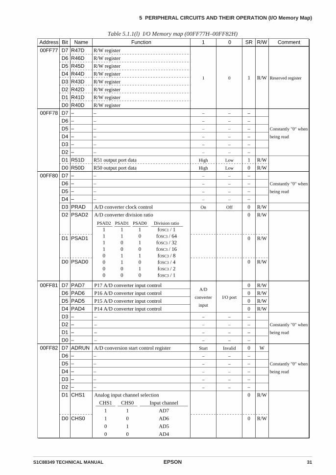
S1C88349 TECHNICAL MANUAL EPSON 31
5 PERIPHERAL CIRCUITS AND THEIR OPERATION (I/O Memory Map)
Table 5.1.1(l) I/O Memory map (00FF77H–00FF82H)
Address Bit Name SR R/WFunction Comment1 0
00FF77 D7
D6
D5
D4
D3
D2
D1
D0
R47D
R46D
R45D
R44D
R43D
R42D
R41D
R40D
R/W register
R/W register
R/W register
R/W register
R/W register
R/W register
R/W register
R/W register
Reserved register1 R/W1 0
00FF78 D7
D6
D5
D4
D3
D2
D1
D0
–
–
–
–
–
–
R51D
R50D
–
–
–
–
–
–
R51 output port data
R50 output port data
Constantly "0" when
being read
–
–
–
–
–
–
1
0
R/W
R/W
–
–
–
–
–
–
High
High
–
–
–
–
–
–
Low
Low
00FF80 D7
D6
D5
D4
D3
D2
D1
D0
–
–
–
–
PRAD
PSAD2
PSAD1
PSAD0
–
–
–
–
A/D converter clock control
A/D converter division ratio
Constantly "0" when
being read
–
–
–
–
0
0
0
0
R/W
R/W
R/W
R/W
–
–
–
–
On
–
–
–
–
Off
PSAD2
11110000
PSAD1
11001100
PSAD0
10101010
Division ratio
fOSC1 / 1fOSC3 / 64fOSC3 / 32fOSC3 / 16fOSC3 / 8fOSC3 / 4fOSC3 / 2fOSC3 / 1
00FF81 D7
D6
D5
D4
D3
D2
D1
D0
PAD7
PAD6
PAD5
PAD4
–
–
–
–
P17 A/D converter input control
P16 A/D converter input control
P15 A/D converter input control
P14 A/D converter input control
–
–
–
–
Constantly "0" when
being read
0
0
0
0
–
–
–
–
R/W
R/W
R/W
R/W
A/D
converter
input
–
–
–
–
I/O port
–
–
–
–
00FF82 D7
D6
D5
D4
D3
D2
D1
D0
ADRUN
–
–
–
–
–
CHS1
CHS0
A/D conversion start control register
–
–
–
–
–
Analog input channel selection
Constantly "0" when
being read
0
–
–
–
–
–
0
0
W
R/W
R/W
Start
–
–
–
–
–
Invalid
–
–
–
–
–
CHS1
1
1
0
0
CHS0
1
0
1
0
Input channel
AD7
AD6
AD5
AD4
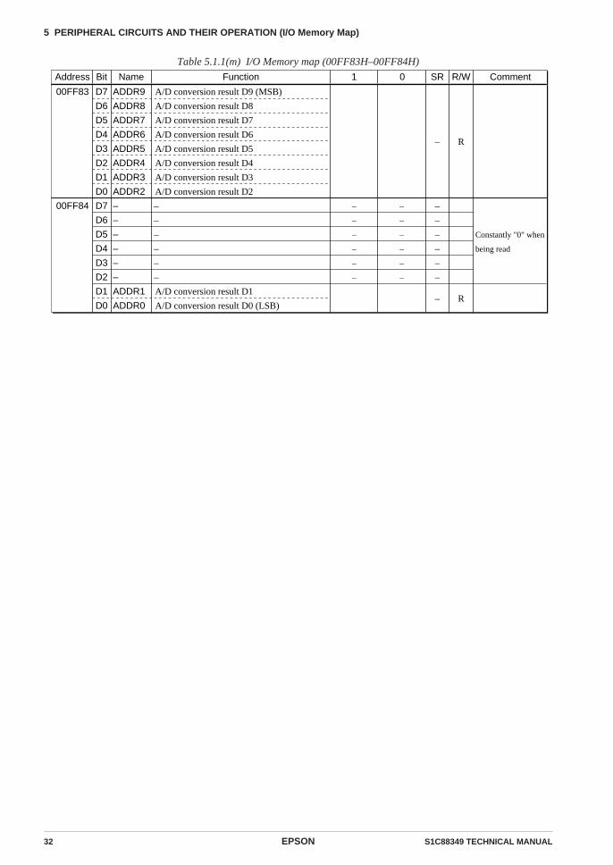
32 EPSON S1C88349 TECHNICAL MANUAL
5 PERIPHERAL CIRCUITS AND THEIR OPERATION (I/O Memory Map)
Table 5.1.1(m) I/O Memory map (00FF83H–00FF84H)
Address Bit Name SR R/WFunction Comment1 0
00FF83 D7
D6
D5
D4
D3
D2
D1
D0
ADDR9
ADDR8
ADDR7
ADDR6
ADDR5
ADDR4
ADDR3
ADDR2
A/D conversion result D9 (MSB)
A/D conversion result D8
A/D conversion result D7
A/D conversion result D6
A/D conversion result D5
A/D conversion result D4
A/D conversion result D3
A/D conversion result D2
– R
00FF84 D7
D6
D5
D4
D3
D2
D1
D0
–
–
–
–
–
–
ADDR1
ADDR0
–
–
–
–
–
–
A/D conversion result D1
A/D conversion result D0 (LSB)
Constantly "0" when
being read
–
–
–
–
–
–
– R
–
–
–
–
–
–
–
–
–
–
–
–
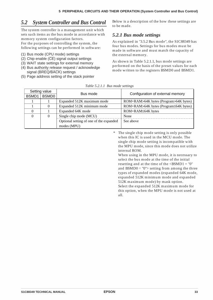
S1C88349 TECHNICAL MANUAL EPSON 33
5 PERIPHERAL CIRCUITS AND THEIR OPERATION (System Controller and Bus Control)
5.2 System Controller and Bus ControlThe system controller is a management unit whichsets such items as the bus mode in accordance withmemory system configuration factors.For the purposes of controlling the system, thefollowing settings can be performed in software:
(1) Bus mode (CPU mode) settings(2) Chip enable (CE) signal output settings(3) WAIT state settings for external memory(4) Bus authority release request / acknowledge
signal (BREQ/BACK) settings(5) Page address setting of the stack pointer
Below is a description of the how these settings areto be made.
5.2.1 Bus mode settingsAs explained in "3.5.2 Bus mode", the S1C88349 hasfour bus modes. Settings for bus modes must bemade in software and must match the capacity ofthe external memory.
As shown in Table 5.2.1.1, bus mode settings areperformed on the basis of the preset values for eachmode written to the registers BSMD0 and BSMD1.
Table 5.2.1.1 Bus mode settings
* The single chip mode setting is only possiblewhen this IC is used in the MCU mode. Thesingle chip mode setting is incompatible withthe MPU mode, since this mode does not utilizeinternal ROM.When using in the MPU mode, it is necessary toselect the bus mode at the time of the initialresetting and at the time of the <BSMD1 = "0"and BSMD0 = "0"> setting from among the threetypes of expanded modes (expanded 64K mode,expanded 512K minimum mode and expanded512K maximum mode) by mask option.Select the expanded 512K maximum mode forthis option, when the MPU mode is not used atall.
BSMD11100
ROM+RAM>64K bytes (Program>64K bytes)ROM+RAM>64K bytes (Program≤64K bytes)ROM+RAM≤64K bytesNoneSee above
Expanded 512K maximum modeExpanded 512K minimum modeExpanded 64K modeSingle chip mode (MCU)Optional setting of one of the expandedmodes (MPU)
Setting valueBus mode Configuration of external memory
BSMD01010
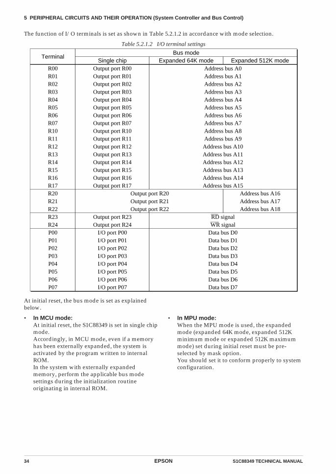
34 EPSON S1C88349 TECHNICAL MANUAL
5 PERIPHERAL CIRCUITS AND THEIR OPERATION (System Controller and Bus Control)
The function of I/O terminals is set as shown in Table 5.2.1.2 in accordance with mode selection.
Table 5.2.1.2 I/O terminal settings
Terminal
R00R01R02R03R04R05R06R07R10R11R12R13R14R15R16R17R20R21R22R23R24P00P01P02P03P04P05P06P07
Output port R00Output port R01Output port R02Output port R03Output port R04Output port R05Output port R06Output port R07
Bus modeExpanded 64K mode Expanded 512K modeSingle chip
Address bus A0Address bus A1Address bus A2Address bus A3Address bus A4Address bus A5Address bus A6Address bus A7Address bus A8Address bus A9
Output port R10Output port R11Output port R12Output port R13Output port R14Output port R15Output port R16Output port R17
Output port R23Output port R24
I/O port P00I/O port P01I/O port P02I/O port P03I/O port P04I/O port P05I/O port P06I/O port P07
Address bus A10Address bus A11Address bus A12Address bus A13Address bus A14Address bus A15
RD signalWR signal
Data bus D0Data bus D1Data bus D2Data bus D3Data bus D4Data bus D5Data bus D6Data bus D7
Output port R20Output port R21Output port R22
Address bus A16Address bus A17Address bus A18
At initial reset, the bus mode is set as explainedbelow.
• In MCU mode:At initial reset, the S1C88349 is set in single chipmode.Accordingly, in MCU mode, even if a memoryhas been externally expanded, the system isactivated by the program written to internalROM.In the system with externally expandedmemory, perform the applicable bus modesettings during the initialization routineoriginating in internal ROM.
• In MPU mode:When the MPU mode is used, the expandedmode (expanded 64K mode, expanded 512Kminimum mode or expanded 512K maximummode) set during initial reset must be pre-selected by mask option.You should set it to conform properly to systemconfiguration.
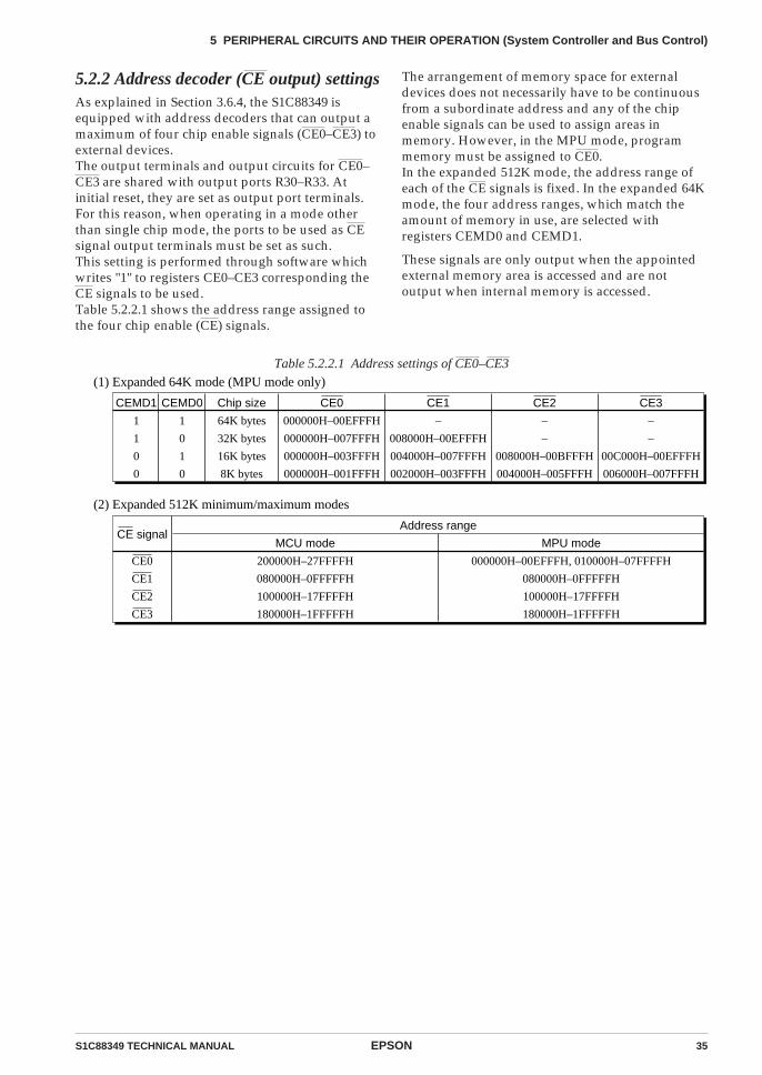
S1C88349 TECHNICAL MANUAL EPSON 35
5 PERIPHERAL CIRCUITS AND THEIR OPERATION (System Controller and Bus Control)
5.2.2 Address decoder (CE output) settingsAs explained in Section 3.6.4, the S1C88349 isequipped with address decoders that can output amaximum of four chip enable signals (CE0–CE3) toexternal devices.The output terminals and output circuits for CE0–CE3 are shared with output ports R30–R33. Atinitial reset, they are set as output port terminals.For this reason, when operating in a mode otherthan single chip mode, the ports to be used as CEsignal output terminals must be set as such.This setting is performed through software whichwrites "1" to registers CE0–CE3 corresponding theCE signals to be used.Table 5.2.2.1 shows the address range assigned tothe four chip enable (CE) signals.
The arrangement of memory space for externaldevices does not necessarily have to be continuousfrom a subordinate address and any of the chipenable signals can be used to assign areas inmemory. However, in the MPU mode, programmemory must be assigned to CE0.In the expanded 512K mode, the address range ofeach of the CE signals is fixed. In the expanded 64Kmode, the four address ranges, which match theamount of memory in use, are selected withregisters CEMD0 and CEMD1.
These signals are only output when the appointedexternal memory area is accessed and are notoutput when internal memory is accessed.
Table 5.2.2.1 Address settings of CE0–CE3
(1) Expanded 64K mode (MPU mode only)
CE0
CE1
CE2
CE3
200000H–27FFFFH
080000H–0FFFFFH
100000H–17FFFFH
180000H–1FFFFFH
000000H–00EFFFH, 010000H–07FFFFH
080000H–0FFFFFH
100000H–17FFFFH
180000H–1FFFFFH
Address rangeCE signal
(2) Expanded 512K minimum/maximum modes
MCU mode MPU mode
1
0
1
0
–
–
00C000H–00EFFFH
006000H–007FFFH
CE3CEMD0
–
–
008000H–00BFFFH
004000H–005FFFH
–
008000H–00EFFFH
004000H–007FFFH
002000H–003FFFH
000000H–00EFFFH
000000H–007FFFH
000000H–003FFFH
000000H–001FFFH
CE2CE1CE0
64K bytes
32K bytes
16K bytes
8K bytes
Chip size
1
1
0
0
CEMD1
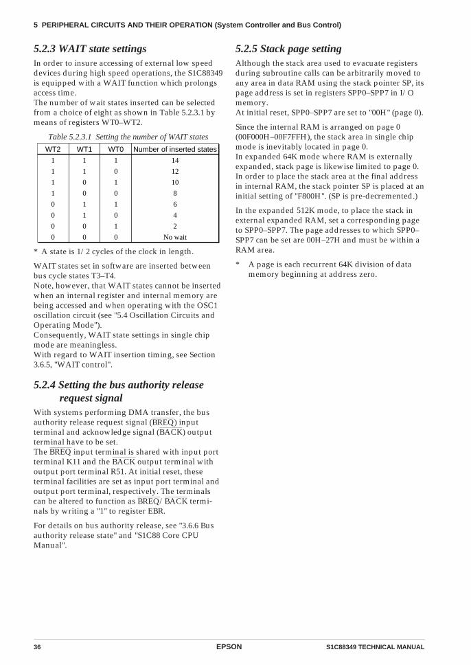
36 EPSON S1C88349 TECHNICAL MANUAL
5 PERIPHERAL CIRCUITS AND THEIR OPERATION (System Controller and Bus Control)
5.2.3 WAIT state settingsIn order to insure accessing of external low speeddevices during high speed operations, the S1C88349is equipped with a WAIT function which prolongsaccess time.The number of wait states inserted can be selectedfrom a choice of eight as shown in Table 5.2.3.1 bymeans of registers WT0–WT2.
Table 5.2.3.1 Setting the number of WAIT states
5.2.5 Stack page settingAlthough the stack area used to evacuate registersduring subroutine calls can be arbitrarily moved toany area in data RAM using the stack pointer SP, itspage address is set in registers SPP0–SPP7 in I/Omemory.At initial reset, SPP0–SPP7 are set to "00H" (page 0).
Since the internal RAM is arranged on page 0(00F000H–00F7FFH), the stack area in single chipmode is inevitably located in page 0.In expanded 64K mode where RAM is externallyexpanded, stack page is likewise limited to page 0.In order to place the stack area at the final addressin internal RAM, the stack pointer SP is placed at aninitial setting of "F800H". (SP is pre-decremented.)
In the expanded 512K mode, to place the stack inexternal expanded RAM, set a corresponding pageto SPP0–SPP7. The page addresses to which SPP0–SPP7 can be set are 00H–27H and must be within aRAM area.
* A page is each recurrent 64K division of datamemory beginning at address zero.
WT2 Number of inserted states
1
1
1
1
0
0
0
0
14
12
10
8
6
4
2
No wait
WT1
1
1
0
0
1
1
0
0
WT0
1
0
1
0
1
0
1
0
* A state is 1/2 cycles of the clock in length.
WAIT states set in software are inserted betweenbus cycle states T3–T4.Note, however, that WAIT states cannot be insertedwhen an internal register and internal memory arebeing accessed and when operating with the OSC1oscillation circuit (see "5.4 Oscillation Circuits andOperating Mode").Consequently, WAIT state settings in single chipmode are meaningless.With regard to WAIT insertion timing, see Section3.6.5, "WAIT control".
5.2.4 Setting the bus authority releaserequest signal
With systems performing DMA transfer, the busauthority release request signal (BREQ) inputterminal and acknowledge signal (BACK) outputterminal have to be set.The BREQ input terminal is shared with input portterminal K11 and the BACK output terminal withoutput port terminal R51. At initial reset, theseterminal facilities are set as input port terminal andoutput port terminal, respectively. The terminalscan be altered to function as BREQ/BACK termi-nals by writing a "1" to register EBR.
For details on bus authority release, see "3.6.6 Busauthority release state" and "S1C88 Core CPUManual".
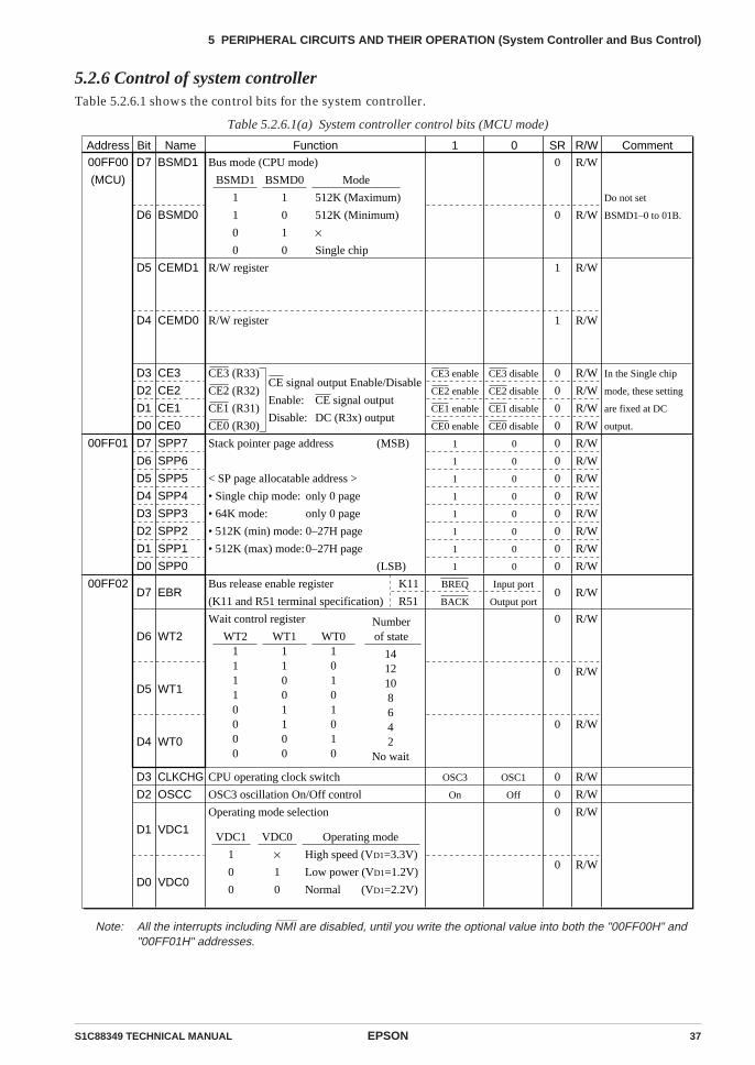
S1C88349 TECHNICAL MANUAL EPSON 37
5 PERIPHERAL CIRCUITS AND THEIR OPERATION (System Controller and Bus Control)
5.2.6 Control of system controllerTable 5.2.6.1 shows the control bits for the system controller.
Table 5.2.6.1(a) System controller control bits (MCU mode)
Note: All the interrupts including NMI are disabled, until you write the optional value into both the "00FF00H" and"00FF01H" addresses.
Address Bit Name00FF00
(MCU)
D7
D6
D5
D4
D3
D2
D1
D0
BSMD1
BSMD0
CEMD1
CEMD0
CE3
CE2
CE1
CE0
SR R/WFunction CommentBus mode (CPU mode)
R/W register
R/W register
CE3 (R33)
CE2 (R32)
CE1 (R31)
CE0 (R30)
Do not set
BSMD1–0 to 01B.
In the Single chip
mode, these setting
are fixed at DC
output.
1 00
0
1
1
0
0
0
0
R/W
R/W
R/W
R/W
R/W
R/W
R/W
R/W
CE3 enable
CE2 enable
CE1 enable
CE0 enable
BSMD1
1
1
0
0
BSMD0
1
0
1
0
Mode
512K (Maximum)
512K (Minimum)
×Single chip
CE signal output
DC (R3x) output
CE signal output Enable/Disable
Enable:
Disable:
CE3 disable
CE2 disable
CE1 disable
CE0 disable
00FF01 D7
D6
D5
D4
D3
D2
D1
D0
SPP7
SPP6
SPP5
SPP4
SPP3
SPP2
SPP1
SPP0
Stack pointer page address
< SP page allocatable address >
• Single chip mode:
• 64K mode:
• 512K (min) mode:
• 512K (max) mode:
0
0
0
0
0
0
0
0
R/W
R/W
R/W
R/W
R/W
R/W
R/W
R/W
1
1
1
1
1
1
1
1
0
0
0
0
0
0
0
0
(MSB)
(LSB)
only 0 page
only 0 page
0–27H page
0–27H page
00FF02D7
D6
D5
D4
D3
D2
D1
D0
EBR
WT2
WT1
WT0
CLKCHG
OSCC
VDC1
VDC0
Bus release enable register
(K11 and R51 terminal specification)
Wait control register
CPU operating clock switch
OSC3 oscillation On/Off control
Operating mode selection
0
0
0
0
0
0
0
0
R/W
R/W
R/W
R/W
R/W
R/W
R/W
R/W
BREQ
BACK
OSC3
On
WT211110000
WT111001100
Numberof state
1412108642
No wait
Input port
Output port
OSC1
Off
K11
R51
VDC1
1
0
0
VDC0
×1
0
High speed (VD1=3.3V)
Low power (VD1=1.2V)
Normal (VD1=2.2V)
WT010101010
Operating mode

38 EPSON S1C88349 TECHNICAL MANUAL
5 PERIPHERAL CIRCUITS AND THEIR OPERATION (System Controller and Bus Control)
Table 5.2.6.1(b) System controller control bits (MPU mode)
Note: All the interrupts including NMI are disabled, until you write the optional value into both the "00FF00H" and"00FF01H" addresses.
Address Bit Name SR R/WFunction Comment1 000FF00
(MPU)
D7
D6
D5
D4
D3
D2
D1
D0
BSMD1
BSMD0
CEMD1
CEMD0
CE3
CE2
CE1
CE0
Bus mode (CPU mode)
Chip enable mode
CE3 (R33)
CE2 (R32)
CE1 (R31)
CE0 (R30)
R/W
R/W
R/W
R/W
R/W
R/W
R/W
R/W
CE3 enable
CE2 enable
CE1 enable
CE0 enable
CE3 disable
CE2 disable
CE1 disable
CE0 disable
BSMD1
1
1
0
0
BSMD0
1
0
1
0
Mode
CE signal output
DC (R3x) output
CE signal output Enable/Disable
Enable:
Disable:
00FF01 D7
D6
D5
D4
D3
D2
D1
D0
SPP7
SPP6
SPP5
SPP4
SPP3
SPP2
SPP1
SPP0
Stack pointer page address
< SP page allocatable address >
• Single chip mode:
• 64K mode:
• 512K (min) mode:
• 512K (max) mode:
0
0
0
0
0
0
0
0
R/W
R/W
R/W
R/W
R/W
R/W
R/W
R/W
1
1
1
1
1
1
1
1
0
0
0
0
0
0
0
0
(MSB)
(LSB)
only 0 page
only 0 page
0–27H page
0–27H page
00FF02D7
D6
D5
D4
D3
D2
D1
D0
EBR
WT2
WT1
WT0
CLKCHG
OSCC
VDC1
VDC0
Bus release enable register
(K11 and R51 terminal specification)
Wait control register
CPU operating clock switch
OSC3 oscillation On/Off control
Operating mode selection
BREQ
BACK
OSC3
On
WT211110000
WT111001100
Numberof state
1412108642
No wait
Input port
Output port
OSC1
Off
K11
R51
VDC1
1
0
0
VDC0
×1
0
Operating mode
WT010101010
CEMD1
1
1
0
0
CEMD0
1
0
1
0
Mode
64K (CE0)
32K (CE0, CE1)
16K (CE0–CE3)
8K (CE0–CE3)
0
0
0
0
0
0
0
0
R/W
R/W
R/W
R/W
R/W
R/W
R/W
R/WHigh speed (VD1=3.3V)
Low power (VD1=1.2V)
Normal (VD1=2.2V)
* Initial setting can
be selected among 3
types (64K, 512K
min and 512K max)
by mask option
setting.
Only for 64K
bus mode
*
*
1
1
0
0
0
1
512K (Maximum)
512K (Minimum)
64K
* Option selection

S1C88349 TECHNICAL MANUAL EPSON 39
5 PERIPHERAL CIRCUITS AND THEIR OPERATION (System Controller and Bus Control)
CE0–CE3: 00FF00H•D0–D3Sets the CE output terminals being used.
When "1" is written: CE output enableWhen "0" is written: CE output disableReading: Valid
CE output is enabled when a "1" is written toregisters CE0–CE3 which correspond to the CEoutput being used. A "0" written to any of theregisters disables CE signal output from thatterminal and it reverts to its alternate function as anoutput port terminal (R30–R33).At initial reset, register CE0 is set to "0" in the MCUmode and in the MPU mode, "1" is set in theregister. Registers CE1–CE3 are always set to "0"regardless of the MCU/MPU mode setting.
Note: To avoid a malfunction from an interruptgenerated before the bus configuration isinitialized, all interrupts including NMI aremasked until you write an optional value intoaddress "00FF00H".
SPP0–SPP7: 00FF01HSets the page address of stack area. In single chipmode and expanded 64K mode, set page address to"00H".In expanded 512K mode, it can be set to any valuewithin the range "00H"–"27H".Since a carry and borrow from/to the stack pointerSP is not reflected in register SPP, the upper limiton continuous use of the stack area is 64K bytes.At initial reset, this register is set to "00H" (page 0).
Note: To avoid a malfunction from an interruptgenerated before the bus configuration isinitialized, all interrupts including NMI aredisabled, until you write an optional valueinto "00FF01H" address. Furthermore, toavoid generating an interrupt while the stackarea is being set, all interrupts including NMIare disabled in one instruction executionperiod after writing to address "00FF01H".
BSMD0, BSMD1: 00FF00H•D6, D7Bus modes are set as shown in Table 5.2.6.2.
Table 5.2.6.2 Bus mode settings
BSMD1Bus mode
1
1
0
0
Expanded 512K maximum mode
Expanded 512K minimum mode
Expanded 64K mode
Single chip mode (MCU)
Optional setting of one of the
expanded modes (MPU)
BSMD0
1
0
1
0
Setting values
The single chip mode setting is only possible whenthis IC is used in the MCU mode. The single chipmode setting is incompatible with the MPU mode,since this mode does not utilize internal ROM.When using in the MPU mode, it is necessary toselect the bus mode at the time of the initial reset-ting and at the time of the <BSMD1 = "0" andBSMD0 = "0"> setting from among the three typesof expanded modes (expanded 64K mode, ex-panded 512K minimum mode and expanded 512Kmaximum mode) by mask option.Select the expanded 512K maximum mode for thisoption, when the MPU mode is not used at all.At initial reset, in the MCU mode the unit is set tosingle chip mode and in the MPU mode the maskoption is used to select the applicable mode.
CEMD0, CEMD1: 00FF00H•D4, D5Sets the CE signal address range (valid only in theexpanded 64K mode∗).Settings are made according to external memorychip size as shown in Table 5.2.6.3.
Table 5.2.6.3 CE signal settings
CEMD1 Usable terminals
1
1
0
0
CE0
CE0, CE1
CE0–CE3
CE0–CE3
CEMD0
1
0
1
0
Address range
64K bytes
32K bytes
16K bytes
8K bytes
These settings are invalid for any mode other thanexpanded 64K mode.At initial reset, each register is set to "1" (64K bytes).
∗ Settings of these registers are valid only in theMPU mode. CEMD0 and CEMD1 can be used asgeneral purpose registers with read/writecapabilities in the MCU mode.
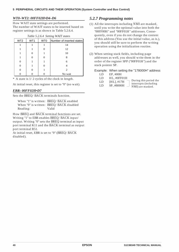
40 EPSON S1C88349 TECHNICAL MANUAL
5 PERIPHERAL CIRCUITS AND THEIR OPERATION (System Controller and Bus Control)
WT0–WT2: 00FF02H•D4–D6How WAIT state settings are performed.The number of WAIT states to be inserted based onregister settings is as shown in Table 5.2.6.4.
Table 5.2.6.4 Setting WAIT states
* A state is 1/2 cycles of the clock in length.
At initial reset, this register is set to "0" (no wait).
EBR: 00FF02H•D7Sets the BREQ/BACK terminals function.
When "1" is written: BREQ/BACK enabledWhen "0" is written: BREQ/BACK disabledReading: Valid
How BREQ and BACK terminal functions are set.Writing "1" to EBR enables BREQ/BACK input/output. Writing "0" sets the BREQ terminal as inputport terminal K11 and the BACK terminal as outputport terminal R51.At initial reset, EBR is set to "0" (BREQ/BACKdisabled).
5.2.7 Programming notes(1) All the interrupts including NMI are masked,
until you write the optional value into both the"00FF00H" and "00FF01H" addresses. Conse-quently, even if you do not change the contentof this address (You use the initial value, as is.),you should still be sure to perform the writingoperation using the initialization routine.
(2) When setting stack fields, including pageaddresses as well, you should write them in theorder of the register SPP ("00FF01H") and thestack pointer SP.
Example: When setting the "178000H" addressLD EP, #00HLD HL, #0FF01HLD [HL], #17HLD SP, #8000H
During this period theinterrupts (includingNMI) are masked.
WT2 Number of inserted states
1
1
1
1
0
0
0
0
14
12
10
8
6
4
2
No wait
WT1
1
1
0
0
1
1
0
0
WT0
1
0
1
0
1
0
1
0

S1C88349 TECHNICAL MANUAL EPSON 41
5 PERIPHERAL CIRCUITS AND THEIR OPERATION (Watchdog Timer)
5.3 Watchdog Timer
5.3.1 Configuration of watchdog timerThe S1C88349 is equipped with a watchdog timerdriven by OSC1 as source oscillation. The watchdogtimer must be reset periodically in software, and ifreset of more than 3–4 seconds (when fOSC1 = 32.768kHz) does not take place, a non-maskable interruptsignal is generated and output to the CPU.
Figure 5.3.1.1 is a block diagram of the watchdogtimer.
5.3.2 Interrupt functionIn cases where the watchdog timer is not periodi-cally reset in software, the watchdog timer outputsan interrupt signal to the CPU's NMI (level 4) input.Unmaskable and taking priority over other inter-rupts, this interrupt triggers the generation ofexception processing. See the "S1C88 Core CPUManual" for more details on NMI exceptionprocessing.This exception processing vector is set at 000004H.
5.3.3 Control of watchdog timerTable 5.3.3.1 shows the control bits for the watch-dog timer.
WDRST: 00FF40H•D2Resets the watchdog timer.
When "1" is written: Watchdog timer is resetWhen "0" is written: No operationReading: Constantly "0"
By writing "1" to WDRST, the watchdog timer isreset, after which it is immediately restarted.Writing "0" will mean no operation.Since WDRST is for writing only, it is constantly setto "0" during readout.
5.3.4 Programming notes(1) The watchdog timer must reset within 3-second
cycles by software.
(2) Do not execute the SLP instruction for 2 msecafter a NMI interrupt has occurred (when fOSC1
is 32.768 kHz).
Table 5.3.3.1 Watchdog timer control bitsAddress Bit Name
00FF40 D7
D6
D5
D4
D3
D2
D1
D0
–
FOUT2
FOUT1
FOUT0
FOUTON
WDRST
TMRST
TMRUN
SR R/WFunction Comment
–
FOUT frequency selection
FOUT output control
Watchdog timer reset
Clock timer reset
Clock timer Run/Stop control
"0" when being read
Constantly "0" when
being read
1 0
–
0
0
0
0
–
–
0
R/W
R/W
R/W
R/W
W
W
R/W
–
On
Reset
Reset
Run
–
Off
No operation
No operation
Stop
FOUT2
00001111
FOUT1
00110011
FOUT0
01010101
Frequency
fOSC1 / 1fOSC1 / 2fOSC1 / 4fOSC1 / 8fOSC3 / 1fOSC3 / 2fOSC3 / 4fOSC3 / 8
Fig. 5.3.1.1 Block diagram of watchdog timer
By running watchdog timer reset during the mainroutine of the program, it is possible to detectprogram runaway as if watchdog timer processinghad not been applied. Normally, this routine isintegrated at points that are regularly beingprocessed.
The watchdog timer continues to operate duringHALT and when a HALT state is continuous forlonger than 3–4 seconds, the CPU shifts to excep-tion processing.During SLEEP, the watchdog timer is stopped.
1 Hz
Watchdog timerreset signal
Non-maskableinterrupt (NMI)
Watchdogtimer
Divider
WDRST
fOSC1OSC1oscillationcircuit

42 EPSON S1C88349 TECHNICAL MANUAL
5 PERIPHERAL CIRCUITS AND THEIR OPERATION (Oscillation Circuits and Operating Mode)
5.4 Oscillation Circuits andOperating Mode
5.4.1 Configuration of oscillation circuitsThe S1C88349 is twin clock system with twointernal oscillation circuits (OSC1 and OSC3).OSC1 oscillation circuit generates the 32.768 kHz(Typ.) main clock and OSC3 oscillation circuit thesub-clock when the CPU and some peripheralcircuits (output port, serial interface and program-mable timer) are in high speed operation.Figure 5.4.1.1 shows the configuration of theoscillation circuit.
5.4.3 OSC1 oscillation circuitThe OSC1 oscillation circuit generates the 32.768 kHz(Typ.) system clock which is utilized during lowspeed operation (low power mode) of the CPU andperipheral circuits. Furthermore, even when OSC3 isutilized as the system clock, OSC1 continues togenerate the source clock for the clock timer andstopwatch timer.This oscillation circuit stops when the SLP instruc-tion is executed. However, in case the SVD circuit isexecuting an SLP instruction, oscillation is stoppedin synchronization with the completion of sampling.In terms of the oscillation circuit types, eithercrystal oscillation, CR oscillation, crystal oscillation(gate capacitor built-in) or external clock input canbe selected with the mask option.Figure 5.4.3.1 shows the configuration of the OSC1oscillation circuit.
Fig. 5.4.1.1 Configuration of oscillation circuits
At initial reset, OSC1 oscillation circuit is selectedfor the CPU operating clock and OSC3 oscillationcircuit is in a stopped state. ON/OFF switching ofthe OSC3 oscillation circuit and switching of thesystem clock between OSC1 and OSC3 are control-led in software. OSC3 circuit is utilized when highspeed operation of the CPU and some peripheralcircuits become necessary. Otherwise, OSC1 shouldbe used to generate the operating clock and OSC3circuit placed in a stopped state in order to reducecurrent consumption.
5.4.2 Mask option
OSC1 oscillation circuit Crystal oscillation circuit External clock input CR oscillation circuit Crystal oscillation circuit (gate capacitor built-in)
OSC3 oscillation circuit Crystal oscillation circuit Ceramic oscillation circuit CR oscillation circuit External clock input
In terms of the oscillation circuit types for OSC1,either crystal oscillation, CR oscillation, crystaloscillation (gate capacitor built-in) or external clockinput can be selected with the mask option.In terms of oscillation circuit types for OSC3, eithercrystal oscillation, ceramic oscillation, CR oscilla-tion or external clock input can be selected with themask option, in the same way as OSC1.
(3) CR oscillation circuit
To CPU (CLK)
OSC1oscillation circuit
Clockswitch
OSC3oscillation circuit
To peripheralcircuit (fOSC1)
OSCC
Oscillation circuitcontrol signal
CLKCHG
CPU clockselection signal
To some peripheralcircuit (fOSC3)
SLEEPstatus
OSC2
OSC1
RCR1
fOSC1
SLEEP status
VSSOSC2
OSC1
SLEEP status
fOSC1
X'tal1 VSS
fOSC1
VSSVSS
OSC2
OSC1
X'tal1
CG1
SLEEP status
fOSC1
VSS
SLEEP status
OSC2
OSC1
Externalclock
N.C.
VSS
VDD
(1) Crystal oscillation circuit
(2) External clock input
(4) Crystal oscillation circuit (gate capacitor built-in)
Fig. 5.4.3.1 OSC1 oscillation circuit
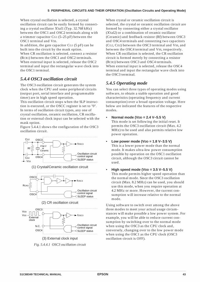
S1C88349 TECHNICAL MANUAL EPSON 43
5 PERIPHERAL CIRCUITS AND THEIR OPERATION (Oscillation Circuits and Operating Mode)
When crystal oscillation is selected, a crystaloscillation circuit can be easily formed by connect-ing a crystal oscillator X'tal1 (Typ. 32.768 kHz)between the OSC1 and OSC2 terminals along witha trimmer capacitor CG1 (5–25 pF) between theOSC1 terminal and VSS.In addition, the gate capacitor CG1 (5 pF) can bebuilt into the circuit by the mask option.When CR oscillation is selected, connect a resistor(RCR1) between the OSC1 and OSC2 terminals.When external input is selected, release the OSC2terminal and input the rectangular wave clock intothe OSC1 terminal.
5.4.4 OSC3 oscillation circuitThe OSC3 oscillation circuit generates the systemclock when the CPU and some peripheral circuits(output port, serial interface and programmabletimer) are in high speed operation.This oscillation circuit stops when the SLP instruc-tion is executed, or the OSCC register is set to "0".In terms of oscillation circuit types, any one ofcrystal oscillation, ceramic oscillation, CR oscilla-tion or external clock input can be selected with themask option.Figure 5.4.4.1 shows the configuration of the OSC3oscillation circuit.
When crystal or ceramic oscillation circuit isselected, the crystal or ceramic oscillation circuit areformed by connecting either a crystal oscillator(X'tal2) or a combination of ceramic oscillator(Ceramic) and feedback resistor (Rf) between OSC3and OSC4 terminals and connecting two capacitors(CG2, CD2) between the OSC3 terminal and VSS, andbetween the OSC4 terminal and VSS, respectively.When CR oscillation is selected, the CR oscillationcircuit is formed merely by connecting a resistor(RCR3) between OSC3 and OSC4 terminals.When external input is selected, release the OSC4terminal and input the rectangular wave clock intothe OSC3 terminal.
5.4.5 Operating modeYou can select three types of operating modes usingsoftware, to obtain a stable operation and goodcharacteristics (operating frequency and currentconsumption) over a broad operation voltage. Herebelow are indicated the features of the respectivemodes.
• Normal mode (VDD = 2.4 V–5.5 V)This mode is set following the initial reset. Itpermits the OSC3 oscillation circuit (Max. 4.2MHz) to be used and also permits relative lowpower operation.
• Low power mode (VDD = 1.8 V–3.5 V)This is a lower power mode than the normalmode. It makes ultra-low power consumptionpossible by operation on the OSC1 oscillationcircuit, although the OSC3 circuit cannot beused.
• High speed mode (VDD = 3.5 V–5.5 V)This mode permits higher speed operation thanthe normal mode. Since the OSC3 oscillationcircuit (Max. 8.2 MHz) can be used, you shoulduse this mode, when you require operation at4.2 MHz or more. However, the current con-sumption will increase relative to the normalmode.
Using software to switch over among the abovethree modes to meet your actual usage circum-stances will make possible a low power system. Forexample, you will be able to reduce current con-sumption by switching over to the normal modewhen using the OSC3 as the CPU clock and,conversely, changing over to the low power modewhen using the OSC1 as the CPU clock (OSC3oscillation circuit is OFF).
VSS
OSC4
OSC3
Rf
CD2
CG2
fOSC3
Oscillation circuitcontrol signalSLEEP status
X'tal 2 orCeramic
Oscillation circuitcontrol signalSLEEP status
OSC4
OSC3
RCR3
fOSC3
OSC4
OSC3
Externalclock
N.C.
VSS
VDD
fOSC3
Oscillation circuitcontrol signalSLEEP status
(1) Crystal/Ceramic oscillation circuit
(2) CR oscillation circuit
(3) External clock input
Fig. 5.4.4.1 OSC3 oscillation circuit
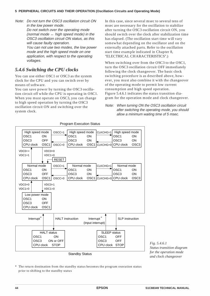
44 EPSON S1C88349 TECHNICAL MANUAL
5 PERIPHERAL CIRCUITS AND THEIR OPERATION (Oscillation Circuits and Operating Mode)
In this case, since several msec to several tens ofmsec are necessary for the oscillation to stabilizeafter turning the OSC3 oscillation circuit ON, youshould switch over the clock after stabilization timehas elapsed. (The oscillation start time will varysomewhat depending on the oscillator and on theexternally attached parts. Refer to the oscillationstart time example indicated in Chapter 8,"ELECTRICAL CHARACTERISTICS".)
When switching over from the OSC3 to the OSC1,turn the OSC3 oscillation circuit OFF immediatelyfollowing the clock changeover. The basic clockswitching procedure is as described above, how-ever, you must also combine it with the changeoverof the operating mode to permit low currentconsumption and high speed operation.Figure 5.4.6.1 indicates the status transition dia-gram for the operation mode and clock changeover.
Note: When turning ON the OSC3 oscillation circuitafter switching the operating mode, you shouldallow a minimum waiting time of 5 msec.
Note: Do not turn the OSC3 oscillation circuit ONin the low power mode.Do not switch over the operating mode(normal mode ↔ high speed mode) in theOSC3 oscillation circuit ON status, as thiswill cause faulty operation.You can not use two modes, the low powermode and the high speed mode on oneapplication, with respect to the operatingvoltages.
5.4.6 Switching the CPU clocksYou can use either OSC1 or OSC3 as the systemclock for the CPU and you can switch over bymeans of software.You can save power by turning the OSC3 oscilla-tion circuit off while the CPU is operating in OSC1.When you must operate on OSC3, you can changeto high speed operation by turning the OSC3oscillation circuit ON and switching over thesystem clock.
* The return destination from the standby status becomes the program execution statusprior to shifting to the standby status
Fig. 5.4.6.1Status transition diagramfor the operation modeand clock changeover
ONON or OFF
STOP
HALT statusOSC1OSC3CPU clock
OFFOFFSTOP
SLEEP statusOSC1OSC3CPU clock
Program Execution Status
Standby Status
HALT instruction SLP instruction*Interrupt *Interrupt(Input interrupt)
VDC0=0
VDC1=0
OSCC=0
RESET
OSCC=1
CLKCHG=0
CLKCHG=1
OSCC=0
OSCC=1
CLKCHG=0
CLKCHG=1
ONOFFOSC1
ONOFFOSC1
ONONOSC1
ONONOSC1
ONONOSC3
ONONOSC3
High speed modeONOFFOSC1
Normal mode
Low power mode
High speed mode
Normal mode
High speed mode
Normal mode
VDC0=
VDC1=1
VDC0=1
VDC1=0
VDC0=0
VDC1=0
×
OSC1OSC3CPU clock
OSC1OSC3CPU clock
OSC1OSC3CPU clock
OSC1OSC3CPU clock
OSC1OSC3CPU clock
OSC1OSC3CPU clock
OSC1OSC3CPU clock
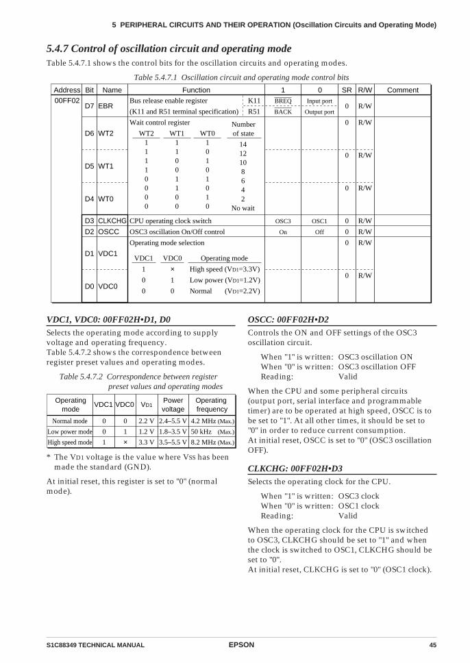
S1C88349 TECHNICAL MANUAL EPSON 45
5 PERIPHERAL CIRCUITS AND THEIR OPERATION (Oscillation Circuits and Operating Mode)
CLKCHG: 00FF02H•D3Selects the operating clock for the CPU.
When "1" is written: OSC3 clockWhen "0" is written: OSC1 clockReading: Valid
When the operating clock for the CPU is switchedto OSC3, CLKCHG should be set to "1" and whenthe clock is switched to OSC1, CLKCHG should beset to "0".At initial reset, CLKCHG is set to "0" (OSC1 clock).
5.4.7 Control of oscillation circuit and operating modeTable 5.4.7.1 shows the control bits for the oscillation circuits and operating modes.
Table 5.4.7.1 Oscillation circuit and operating mode control bits
VDC1, VDC0: 00FF02H•D1, D0Selects the operating mode according to supplyvoltage and operating frequency.Table 5.4.7.2 shows the correspondence betweenregister preset values and operating modes.
Table 5.4.7.2 Correspondence between register preset values and operating modes
OSCC: 00FF02H•D2Controls the ON and OFF settings of the OSC3oscillation circuit.
When "1" is written: OSC3 oscillation ONWhen "0" is written: OSC3 oscillation OFFReading: Valid
When the CPU and some peripheral circuits(output port, serial interface and programmabletimer) are to be operated at high speed, OSCC is tobe set to "1". At all other times, it should be set to"0" in order to reduce current consumption.At initial reset, OSCC is set to "0" (OSC3 oscillationOFF).
2.4–5.5 V
1.8–3.5 V
3.5–5.5 V
Operating frequency
4.2 MHz
50 kHz
8.2 MHz
VD1
2.2 V
1.2 V
3.3 V
VDC1
0
0
1
VDC0
0
1
×
Normal mode
Low power mode
High speed mode
(Max.)
(Max.)
(Max.)
Operatingmode
Powervoltage
* The VD1 voltage is the value where VSS has beenmade the standard (GND).
At initial reset, this register is set to "0" (normalmode).
Address Bit Name SR R/WFunction Comment1 000FF02
D7
D6
D5
D4
D3
D2
D1
D0
EBR
WT2
WT1
WT0
CLKCHG
OSCC
VDC1
VDC0
Bus release enable register
(K11 and R51 terminal specification)
Wait control register
CPU operating clock switch
OSC3 oscillation On/Off control
Operating mode selection
0
0
0
0
0
0
0
0
R/W
R/W
R/W
R/W
R/W
R/W
R/W
R/W
BREQ
BACK
OSC3
On
WT211110000
WT111001100
Numberof state
1412108642
No wait
Input port
Output port
OSC1
Off
K11
R51
VDC1
1
0
0
VDC0
×1
0
High speed (VD1=3.3V)
Low power (VD1=1.2V)
Normal (VD1=2.2V)
WT010101010
Operating mode
46 EPSON S1C88349 TECHNICAL MANUAL
5 PERIPHERAL CIRCUITS AND THEIR OPERATION (Oscillation Circuits and Operating Mode)
5.4.8 Programming notes(1) When the high speed CPU operation is not
necessary, you should operate the peripheralcircuits according to the setting outline indicatebelow.
• CPU operating clockOSC1
• OSC3 oscillation circuitOFF (When the OSC3 clock is not necessaryfor some peripheral circuits.)
• Operating modeLow power mode (When VDD–VSS is 3.5 Vor less)or Normal mode (When VDD–VSS is 3.5 V ormore)
(2) Do not turn the OSC3 oscillation circuit ON inthe low power mode.Do not switch over the operating mode (normalmode ↔ high speed mode) in the OSC3 oscilla-tion circuit ON status, as this will cause faultyoperation.
(3) When turning ON the OSC3 oscillation circuitafter switching the operating mode, you shouldallow a minimum waiting time of 5 msec.
(4) Since several msec to several tens of msec arenecessary for the oscillation to stabilize afterturning the OSC3 oscillation circuit ON.Consequently, you should switch the CPUoperating clock (OSC1 → OSC3) after allowingfor a sufficient waiting time once the OSC3oscillation goes ON. (The oscillation start timewill vary somewhat depending on the oscillatorand on the externally attached parts. Refer tothe oscillation start time example indicated inChapter 8, "ELECTRICAL CHARACTERIS-TICS".)
(5) When switching the clock from OSC3 to OSC1,be sure to switch OSC3 oscillation OFF withseparate instructions. Using a single instructionto process simultaneously can cause a malfunc-tion of the CPU.
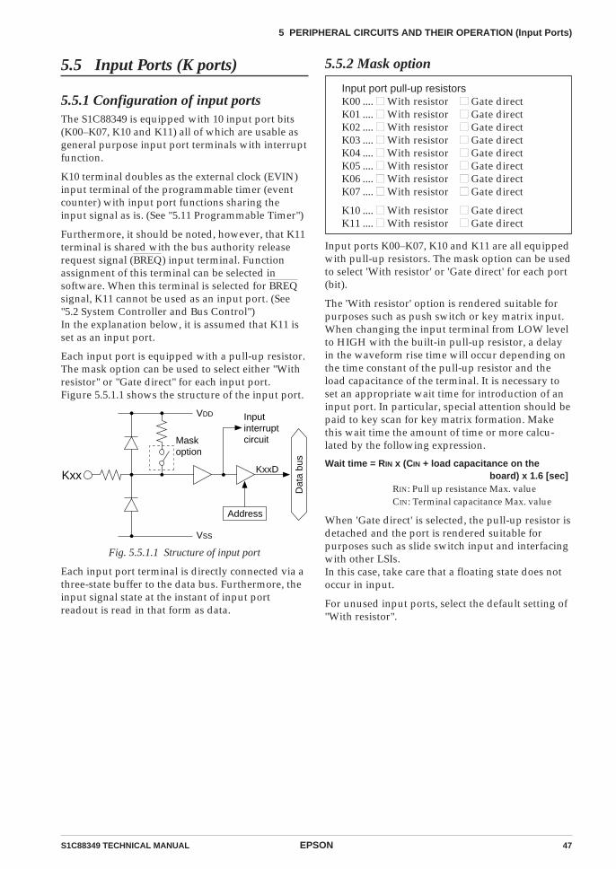
S1C88349 TECHNICAL MANUAL EPSON 47
5 PERIPHERAL CIRCUITS AND THEIR OPERATION (Input Ports)
5.5 Input Ports (K ports)
5.5.1 Configuration of input portsThe S1C88349 is equipped with 10 input port bits(K00–K07, K10 and K11) all of which are usable asgeneral purpose input port terminals with interruptfunction.
K10 terminal doubles as the external clock (EVIN)input terminal of the programmable timer (eventcounter) with input port functions sharing theinput signal as is. (See "5.11 Programmable Timer")
Furthermore, it should be noted, however, that K11terminal is shared with the bus authority releaserequest signal (BREQ) input terminal. Functionassignment of this terminal can be selected insoftware. When this terminal is selected for BREQsignal, K11 cannot be used as an input port. (See"5.2 System Controller and Bus Control")In the explanation below, it is assumed that K11 isset as an input port.
Each input port is equipped with a pull-up resistor.The mask option can be used to select either "Withresistor" or "Gate direct" for each input port.Figure 5.5.1.1 shows the structure of the input port.
Fig. 5.5.1.1 Structure of input port
Each input port terminal is directly connected via athree-state buffer to the data bus. Furthermore, theinput signal state at the instant of input portreadout is read in that form as data.
5.5.2 Mask option
Input port pull-up resistorsK00 .... With resistor Gate directK01 .... With resistor Gate directK02 .... With resistor Gate directK03 .... With resistor Gate directK04 .... With resistor Gate directK05 .... With resistor Gate directK06 .... With resistor Gate directK07 .... With resistor Gate direct
K10 .... With resistor Gate directK11 .... With resistor Gate direct
Input ports K00–K07, K10 and K11 are all equippedwith pull-up resistors. The mask option can be usedto select 'With resistor' or 'Gate direct' for each port(bit).
The 'With resistor' option is rendered suitable forpurposes such as push switch or key matrix input.When changing the input terminal from LOW levelto HIGH with the built-in pull-up resistor, a delayin the waveform rise time will occur depending onthe time constant of the pull-up resistor and theload capacitance of the terminal. It is necessary toset an appropriate wait time for introduction of aninput port. In particular, special attention should bepaid to key scan for key matrix formation. Makethis wait time the amount of time or more calcu-lated by the following expression.
Wait time = RIN x (CIN + load capacitance on the board) x 1.6 [sec]
RIN: Pull up resistance Max. valueCIN: Terminal capacitance Max. value
When 'Gate direct' is selected, the pull-up resistor isdetached and the port is rendered suitable forpurposes such as slide switch input and interfacingwith other LSIs.In this case, take care that a floating state does notoccur in input.
For unused input ports, select the default setting of"With resistor".
Inputinterruptcircuit
VDD
VSS
Dat
a bu
s
Kxx KxxD
Address
Maskoption
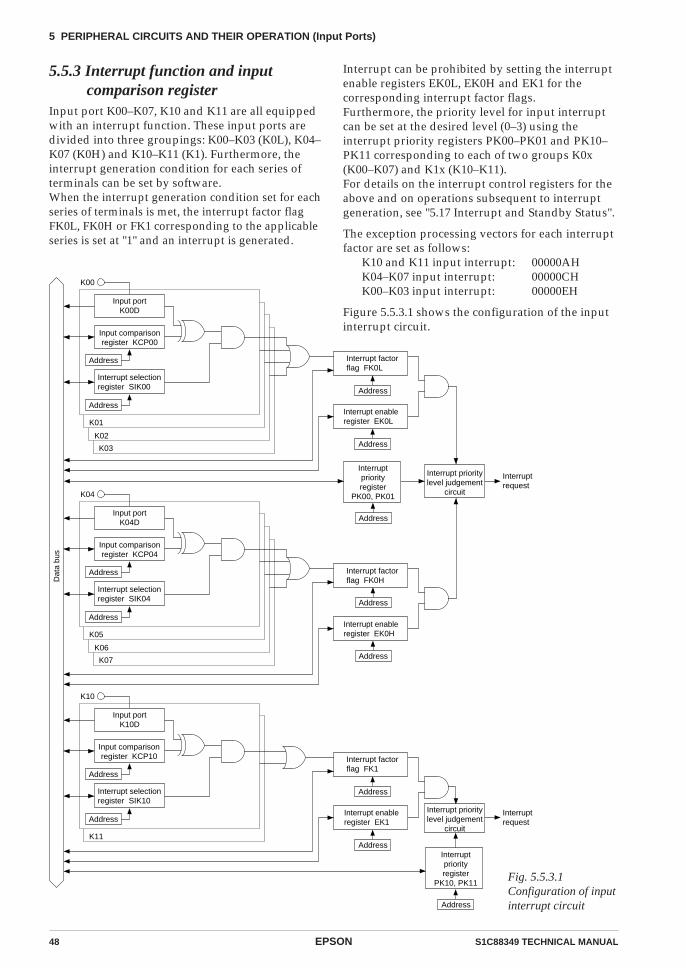
48 EPSON S1C88349 TECHNICAL MANUAL
5 PERIPHERAL CIRCUITS AND THEIR OPERATION (Input Ports)
5.5.3 Interrupt function and inputcomparison register
Input port K00–K07, K10 and K11 are all equippedwith an interrupt function. These input ports aredivided into three groupings: K00–K03 (K0L), K04–K07 (K0H) and K10–K11 (K1). Furthermore, theinterrupt generation condition for each series ofterminals can be set by software.When the interrupt generation condition set for eachseries of terminals is met, the interrupt factor flagFK0L, FK0H or FK1 corresponding to the applicableseries is set at "1" and an interrupt is generated.
Interrupt can be prohibited by setting the interruptenable registers EK0L, EK0H and EK1 for thecorresponding interrupt factor flags.Furthermore, the priority level for input interruptcan be set at the desired level (0–3) using theinterrupt priority registers PK00–PK01 and PK10–PK11 corresponding to each of two groups K0x(K00–K07) and K1x (K10–K11).For details on the interrupt control registers for theabove and on operations subsequent to interruptgeneration, see "5.17 Interrupt and Standby Status".
The exception processing vectors for each interruptfactor are set as follows:
K10 and K11 input interrupt: 00000AHK04–K07 input interrupt: 00000CHK00–K03 input interrupt: 00000EH
Figure 5.5.3.1 shows the configuration of the inputinterrupt circuit.
Dat
a bu
s
K00
Input comparisonregister KCP00
Address
Address
K01
K02
K03
Input portK00D
Interrupt factorflag FK0L
Address
K04
Input comparisonregister KCP04
Address
Address
K05
K06
K07
Input portK04D
Address
K10
Input comparisonregister KCP10
Interrupt selectionregister SIK00
Interrupt selectionregister SIK04
Interrupt selectionregister SIK10
Address
Address
K11
Input portK10D
Interrupt prioritylevel judgement
circuit
Interruptpriorityregister
PK00, PK01
Interrupt prioritylevel judgement
circuit
Interruptpriorityregister
PK10, PK11
Interruptrequest
Interruptrequest
Interrupt enableregister EK0L
Address
Address
Interrupt factorflag FK1
Address
Interrupt enableregister EK1
Address
Interrupt factorflag FK0H
Interrupt enableregister EK0H
Address
Address
Fig. 5.5.3.1Configuration of inputinterrupt circuit
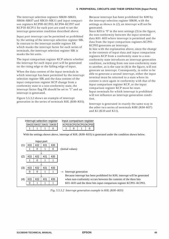
S1C88349 TECHNICAL MANUAL EPSON 49
5 PERIPHERAL CIRCUITS AND THEIR OPERATION (Input Ports)
The interrupt selection registers SIK00–SIK03,SIK04–SIK07 and SIK10–SIK11 and input compari-son registers KCP00–KCP03, KCP04–KCP07 andKCP10–KCP11 for each port are used to set theinterrupt generation condition described above.
Input port interrupt can be permitted or prohibitedby the setting of the interrupt selection register SIK.In contrast to the interrupt enable register EKwhich masks the interrupt factor for each series ofterminals, the interrupt selection register SIK ismasks the bit units.
The input comparison register KCP selects whetherthe interrupt for each input port will be generatedon the rising edge or the falling edge of input.
When the data content of the input terminals inwhich interrupt has been permitted by the interruptselection register SIK and the data content of theinput comparison register KCP change from aconformity state to a non-conformity state, theinterrupt factor flag FK should be set to "1" and aninterrupt is generated.
Figure 5.5.3.2 shows an example of interruptgeneration in the series of terminals K0L (K00–K03).
Because interrupt has been prohibited for K00 bythe interrupt selection register SIK00, with thesettings as shown in (2), an interrupt will not begenerated.Since K03 is "0" in the next settings (3) in the figure,the non-conformity between the input terminaldata K01–K03 where interrupt is permitted and thedata from the input comparison registers KCP01–KCP03 generates an interrupt.In line with the explanation above, since the changein the contents of input data and input comparisonregisters KCP from a conformity state to a non-conformity state introduces an interrupt generationcondition, switching from one non-conformity stateto another, as is the case in (4) in the figure, will notgenerate an interrupt. Consequently, in order to beable to generate a second interrupt, either the inputterminal must be returned to a state where itscontent is once again in conformity with that of theinput comparison register KCP, or the inputcomparison register KCP must be reset.Input terminals for which interrupt is prohibitedwill not influence an interrupt generation condi-tion.
Interrupt is generated in exactly the same way inthe other two series of terminals K0H (K04–K07)and K1 (K10 and K11).
SIK03 SIK011 1
SIK021
SIK000
Interrupt selection registerKCP03 KCP01
1 1KCP02
0KCP00
0
Input comparison register
With the settings shown above, interrupt of K0L (K00–K03) is generated under the condition shown below.
K03 K011 1
K020
K000
Input port(1)
K03 K011 1
K020
K001
(2)
K03 K010 1
K020
K001
(3)
K03 K010 1
K021
K001
(4)
(Initial values)
→ Interrupt generationBecause interrupt has been prohibited for K00, interrupt will be generatedwhen non-conformity occurs between the contents of the three bitsK01–K03 and the three bits input comparison register KCP01–KCP03.
↓
↓
↓
Fig. 5.5.3.2 Interrupt generation example in K0L (K00–K03)
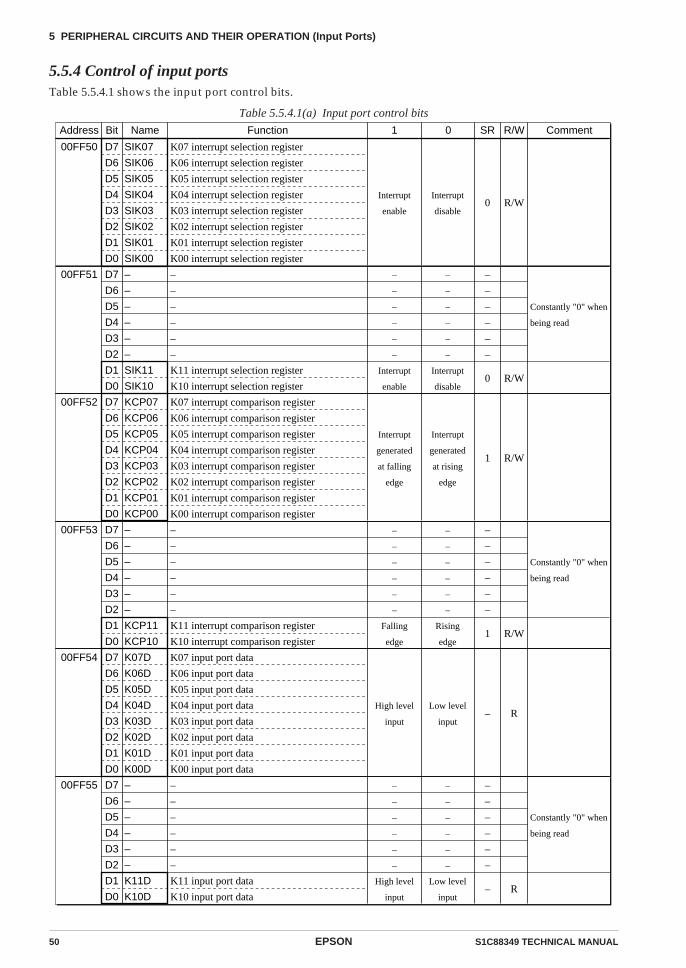
50 EPSON S1C88349 TECHNICAL MANUAL
5 PERIPHERAL CIRCUITS AND THEIR OPERATION (Input Ports)
5.5.4 Control of input portsTable 5.5.4.1 shows the input port control bits.
Table 5.5.4.1(a) Input port control bits
Address Bit Name
00FF50 D7
D6
D5
D4
D3
D2
D1
D0
SIK07
SIK06
SIK05
SIK04
SIK03
SIK02
SIK01
SIK00
SR R/WFunction Comment
K07 interrupt selection register
K06 interrupt selection register
K05 interrupt selection register
K04 interrupt selection register
K03 interrupt selection register
K02 interrupt selection register
K01 interrupt selection register
K00 interrupt selection register
1 0
0 R/WInterrupt
enable
Interrupt
disable
00FF51 D7
D6
D5
D4
D3
D2
D1
D0
–
–
–
–
–
–
SIK11
SIK10
–
–
–
–
–
–
K11 interrupt selection register
K10 interrupt selection register
Constantly "0" when
being read
–
–
–
–
–
–
0 R/W
–
–
–
–
–
–
Interrupt
enable
–
–
–
–
–
–
Interrupt
disable
00FF53 D7
D6
D5
D4
D3
D2
D1
D0
–
–
–
–
–
–
KCP11
KCP10
–
–
–
–
–
–
K11 interrupt comparison register
K10 interrupt comparison register
Constantly "0" when
being read
–
–
–
–
–
–
1 R/W
–
–
–
–
–
–
Falling
edge
–
–
–
–
–
–
Rising
edge
00FF52 D7
D6
D5
D4
D3
D2
D1
D0
KCP07
KCP06
KCP05
KCP04
KCP03
KCP02
KCP01
KCP00
K07 interrupt comparison register
K06 interrupt comparison register
K05 interrupt comparison register
K04 interrupt comparison register
K03 interrupt comparison register
K02 interrupt comparison register
K01 interrupt comparison register
K00 interrupt comparison register
1 R/W
Interrupt
generated
at falling
edge
Interrupt
generated
at rising
edge
00FF54 D7
D6
D5
D4
D3
D2
D1
D0
K07D
K06D
K05D
K04D
K03D
K02D
K01D
K00D
K07 input port data
K06 input port data
K05 input port data
K04 input port data
K03 input port data
K02 input port data
K01 input port data
K00 input port data
– RHigh level
input
Low level
input
00FF55 D7
D6
D5
D4
D3
D2
D1
D0
–
–
–
–
–
–
K11D
K10D
–
–
–
–
–
–
K11 input port data
K10 input port data
Constantly "0" when
being read
–
–
–
–
–
–
– R
–
–
–
–
–
–
High level
input
–
–
–
–
–
–
Low level
input
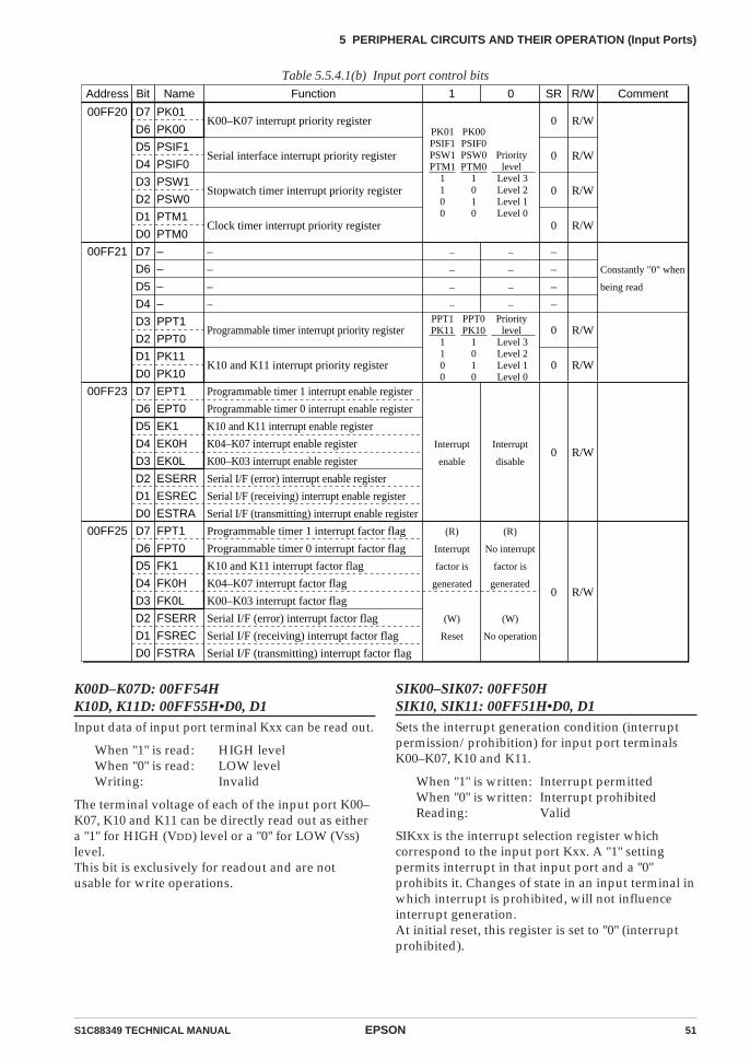
S1C88349 TECHNICAL MANUAL EPSON 51
5 PERIPHERAL CIRCUITS AND THEIR OPERATION (Input Ports)
Table 5.5.4.1(b) Input port control bits
K00D–K07D: 00FF54HK10D, K11D: 00FF55H•D0, D1Input data of input port terminal Kxx can be read out.
When "1" is read: HIGH levelWhen "0" is read: LOW levelWriting: Invalid
The terminal voltage of each of the input port K00–K07, K10 and K11 can be directly read out as eithera "1" for HIGH (VDD) level or a "0" for LOW (VSS)level.This bit is exclusively for readout and are notusable for write operations.
SIK00–SIK07: 00FF50HSIK10, SIK11: 00FF51H•D0, D1Sets the interrupt generation condition (interruptpermission/prohibition) for input port terminalsK00–K07, K10 and K11.
When "1" is written: Interrupt permittedWhen "0" is written: Interrupt prohibitedReading: Valid
SIKxx is the interrupt selection register whichcorrespond to the input port Kxx. A "1" settingpermits interrupt in that input port and a "0"prohibits it. Changes of state in an input terminal inwhich interrupt is prohibited, will not influenceinterrupt generation.At initial reset, this register is set to "0" (interruptprohibited).
Address Bit Name SR R/WFunction Comment1 0
00FF20 D7
D6
D5
D4
D3
D2
D1
D0
PK01
PK00
PSIF1
PSIF0
PSW1
PSW0
PTM1
PTM0
K00–K07 interrupt priority register
Serial interface interrupt priority register
Stopwatch timer interrupt priority register
Clock timer interrupt priority register
0
0
0
0
R/W
R/W
R/W
R/W
PK01PSIF1PSW1PTM1
1100
PK00PSIF0PSW0PTM0
1010
Prioritylevel
Level 3Level 2Level 1Level 0
00FF21 D7
D6
D5
D4
D3
D2
D1
D0
–
–
–
–
PPT1
PPT0
PK11
PK10
–
–
–
–
Programmable timer interrupt priority register
K10 and K11 interrupt priority register
Constantly "0" when
being read
–
–
–
–
0
0
R/W
R/W
–
–
–
–
–
–
–
–PPT1PK11
1100
PPT0PK10
1010
Prioritylevel
Level 3Level 2Level 1Level 0
D7
D6
D5
D4
D3
D2
D1
D0
00FF25 D7
D6
D5
D4
D3
D2
D1
D0
FPT1
FPT0
FK1
FK0H
FK0L
FSERR
FSREC
FSTRA
Programmable timer 1 interrupt factor flag
Programmable timer 0 interrupt factor flag
K10 and K11 interrupt factor flag
K04–K07 interrupt factor flag
K00–K03 interrupt factor flag
Serial I/F (error) interrupt factor flag
Serial I/F (receiving) interrupt factor flag
Serial I/F (transmitting) interrupt factor flag
0 R/W
(R)
Interrupt
factor is
generated
(W)
Reset
(R)
No interrupt
factor is
generated
(W)
No operation
00FF23 EPT1
EPT0
EK1
EK0H
EK0L
ESERR
ESREC
ESTRA
Programmable timer 1 interrupt enable register
Programmable timer 0 interrupt enable register
K10 and K11 interrupt enable register
K04–K07 interrupt enable register
K00–K03 interrupt enable register
Serial I/F (error) interrupt enable register
Serial I/F (receiving) interrupt enable register
Serial I/F (transmitting) interrupt enable register
0 R/WInterrupt
enable
Interrupt
disable
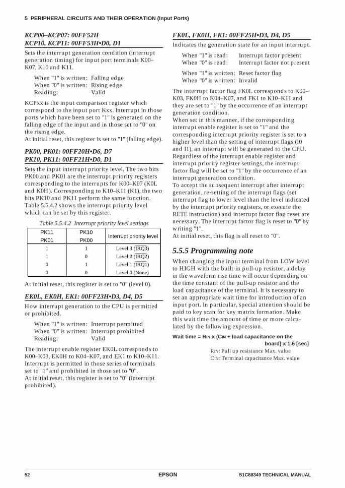
52 EPSON S1C88349 TECHNICAL MANUAL
5 PERIPHERAL CIRCUITS AND THEIR OPERATION (Input Ports)
KCP00–KCP07: 00FF52HKCP10, KCP11: 00FF53H•D0, D1Sets the interrupt generation condition (interruptgeneration timing) for input port terminals K00–K07, K10 and K11.
When "1" is written: Falling edgeWhen "0" is written: Rising edgeReading: Valid
KCPxx is the input comparison register whichcorrespond to the input port Kxx. Interrupt in thoseports which have been set to "1" is generated on thefalling edge of the input and in those set to "0" onthe rising edge.At initial reset, this register is set to "1" (falling edge).
PK00, PK01: 00FF20H•D6, D7PK10, PK11: 00FF21H•D0, D1Sets the input interrupt priority level. The two bitsPK00 and PK01 are the interrupt priority registerscorresponding to the interrupts for K00–K07 (K0Land K0H). Corresponding to K10–K11 (K1), the twobits PK10 and PK11 perform the same function.Table 5.5.4.2 shows the interrupt priority levelwhich can be set by this register.
Table 5.5.4.2 Interrupt priority level settings
FK0L, FK0H, FK1: 00FF25H•D3, D4, D5Indicates the generation state for an input interrupt.
When "1" is read: Interrupt factor presentWhen "0" is read: Interrupt factor not present
When "1" is written: Reset factor flagWhen "0" is written: Invalid
The interrupt factor flag FK0L corresponds to K00–K03, FK0H to K04–K07, and FK1 to K10–K11 andthey are set to "1" by the occurrence of an interruptgeneration condition.When set in this manner, if the correspondinginterrupt enable register is set to "1" and thecorresponding interrupt priority register is set to ahigher level than the setting of interrupt flags (I0and I1), an interrupt will be generated to the CPU.Regardless of the interrupt enable register andinterrupt priority register settings, the interruptfactor flag will be set to "1" by the occurrence of aninterrupt generation condition.To accept the subsequent interrupt after interruptgeneration, re-setting of the interrupt flags (setinterrupt flag to lower level than the level indicatedby the interrupt priority registers, or execute theRETE instruction) and interrupt factor flag reset arenecessary. The interrupt factor flag is reset to "0" bywriting "1".At initial reset, this flag is all reset to "0".
5.5.5 Programming noteWhen changing the input terminal from LOW levelto HIGH with the built-in pull-up resistor, a delayin the waveform rise time will occur depending onthe time constant of the pull-up resistor and theload capacitance of the terminal. It is necessary toset an appropriate wait time for introduction of aninput port. In particular, special attention should bepaid to key scan for key matrix formation. Makethis wait time the amount of time or more calcu-lated by the following expression.
Wait time = RIN x (CIN + load capacitance on the board) x 1.6 [sec]
RIN: Pull up resistance Max. valueCIN: Terminal capacitance Max. value
PK11
PK01
PK10
PK00Interrupt priority level
1
1
0
0
1
0
1
0
Level 3 (IRQ3)
Level 2 (IRQ2)
Level 1 (IRQ1)
Level 0 (None)
At initial reset, this register is set to "0" (level 0).
EK0L, EK0H, EK1: 00FF23H•D3, D4, D5How interrupt generation to the CPU is permittedor prohibited.
When "1" is written: Interrupt permittedWhen "0" is written: Interrupt prohibitedReading: Valid
The interrupt enable register EK0L corresponds toK00–K03, EK0H to K04–K07, and EK1 to K10–K11.Interrupt is permitted in those series of terminalsset to "1" and prohibited in those set to "0".At initial reset, this register is set to "0" (interruptprohibited).
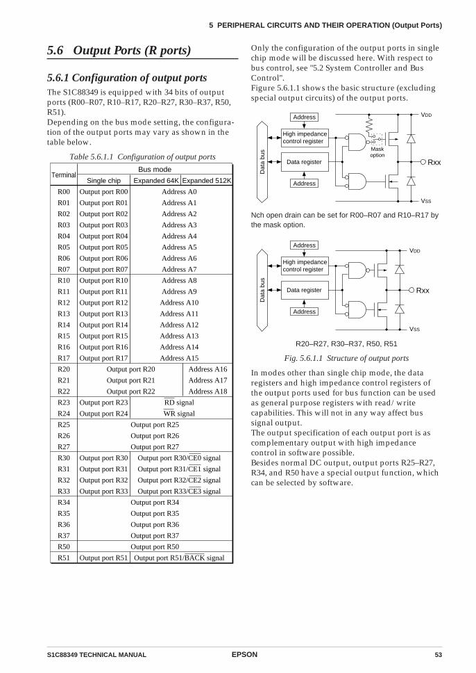
S1C88349 TECHNICAL MANUAL EPSON 53
5 PERIPHERAL CIRCUITS AND THEIR OPERATION (Output Ports)
5.6 Output Ports (R ports)
5.6.1 Configuration of output portsThe S1C88349 is equipped with 34 bits of outputports (R00–R07, R10–R17, R20–R27, R30–R37, R50,R51).Depending on the bus mode setting, the configura-tion of the output ports may vary as shown in thetable below.
Table 5.6.1.1 Configuration of output ports
Only the configuration of the output ports in singlechip mode will be discussed here. With respect tobus control, see "5.2 System Controller and BusControl".Figure 5.6.1.1 shows the basic structure (excludingspecial output circuits) of the output ports.
VDD
VSS
Dat
a bu
s
Rxx
Address
Data register
Address
High impedancecontrol register
Maskoption
Nch open drain can be set for R00–R07 and R10–R17 bythe mask option.
VDD
VSS
Dat
a bu
s
Rxx
Address
Data register
Address
High impedancecontrol register
R20–R27, R30–R37, R50, R51
Fig. 5.6.1.1 Structure of output ports
In modes other than single chip mode, the dataregisters and high impedance control registers ofthe output ports used for bus function can be usedas general purpose registers with read/writecapabilities. This will not in any way affect bussignal output.The output specification of each output port is ascomplementary output with high impedancecontrol in software possible.Besides normal DC output, output ports R25–R27,R34, and R50 have a special output function, whichcan be selected by software.
Terminal
R00
R01
R02
R03
R04
R05
R06
R07
R10
R11
R12
R13
R14
R15
R16
R17
R20
R21
R22
R23
R24
R25
R26
R27
R30
R31
R32
R33
R34
R35
R36
R37
R50
R51
Bus mode
Expanded 64K Expanded 512KSingle chip
Address A0
Address A1
Address A2
Address A3
Address A4
Address A5
Address A6
Address A7
Address A8
Address A9
Address A10
Address A11
Address A12
Address A13
Address A14
Address A15
Output port R20
Output port R21
Output port R22
Address A16
Address A17
Address A18
RD signal
WR signal
Output port R25
Output port R26
Output port R27
Output port R30/CE0 signal
Output port R31/CE1 signal
Output port R32/CE2 signal
Output port R33/CE3 signal
Output port R34
Output port R35
Output port R36
Output port R37
Output port R50
Output port R51/BACK signal
Output port R23
Output port R24
Output port R00
Output port R01
Output port R02
Output port R03
Output port R04
Output port R05
Output port R06
Output port R07
Output port R10
Output port R11
Output port R12
Output port R13
Output port R14
Output port R15
Output port R16
Output port R17
Output port R51
Output port R30
Output port R31
Output port R32
Output port R33

54 EPSON S1C88349 TECHNICAL MANUAL
5 PERIPHERAL CIRCUITS AND THEIR OPERATION (Output Ports)
5.6.2 Mask option
Output ports R00–R07 and R10–R17 outputspecificationsR00 ..... Complementary Nch open drainR01 ..... Complementary Nch open drainR02 ..... Complementary Nch open drainR03 ..... Complementary Nch open drainR04 ..... Complementary Nch open drainR05 ..... Complementary Nch open drainR06 ..... Complementary Nch open drainR07 ..... Complementary Nch open drain
R10 ..... Complementary Nch open drainR11 ..... Complementary Nch open drainR12 ..... Complementary Nch open drainR13 ..... Complementary Nch open drainR14 ..... Complementary Nch open drainR15 ..... Complementary Nch open drainR16 ..... Complementary Nch open drainR17 ..... Complementary Nch open drain
Output ports R00–R07 and R10–R17 can be used toselect output specification for each port (1 bit) bymask option.
The output specification can be selected for eithercomplementary output or Nch open drain output.
Nch open drain output is rendered suitable forpurposes as key matrix common output.
For unused input ports, select the default setting of"Complementary".
Note: When Nch open drain has been selected,voltage in excess of the supply voltagerange must not applied to the output portterminal.
5.6.3 High impedance controlThe output port can be high impedance controlledin software.This makes it possible to share output signal lineswith an other external device.
A high impedance control register is set for eachseries of output port terminals as shown below.Either complementary output and high impedancestate can be selected with this register.
Table 5.6.3.1 Correspondence between output ports and high impedance control registers
* This is a 2-bit reserved register, it can be used asa general purpose register with read/writecapabilities.
When a high impedance control register HZRxx isset to "1", the corresponding output port terminalbecomes high impedance state and when set to "0",it becomes complementary output.
Register Output port terminalHZR0LHZR0HHZR1LHZR1HHZR20HZR21HZR22HZR23HZR24HZR25HZR26HZR27HZR30HZR31HZR32HZR33HZR34HZR35HZR36HZR37HZR4LHZR4HHZR50HZR51
R00–R03R04–R07R10–R13R14–R17
R20R21R22R23R24R25R26R27R30R31R32R33R34R35R36R37
––
R50R51
*
*
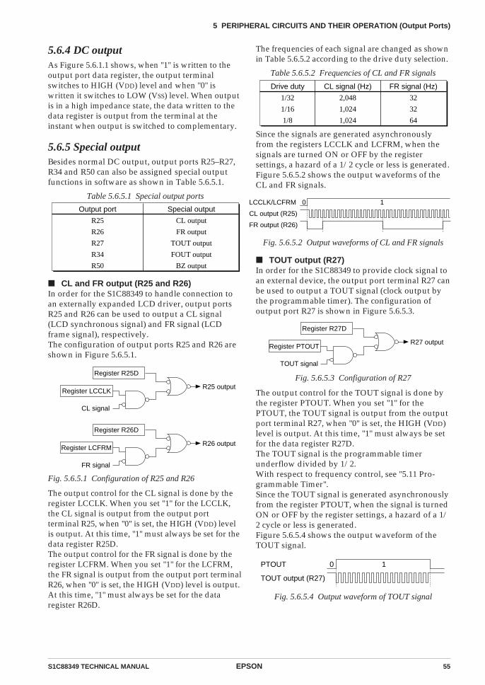
S1C88349 TECHNICAL MANUAL EPSON 55
5 PERIPHERAL CIRCUITS AND THEIR OPERATION (Output Ports)
5.6.4 DC outputAs Figure 5.6.1.1 shows, when "1" is written to theoutput port data register, the output terminalswitches to HIGH (VDD) level and when "0" iswritten it switches to LOW (VSS) level. When outputis in a high impedance state, the data written to thedata register is output from the terminal at theinstant when output is switched to complementary.
5.6.5 Special outputBesides normal DC output, output ports R25–R27,R34 and R50 can also be assigned special outputfunctions in software as shown in Table 5.6.5.1.
Table 5.6.5.1 Special output ports
The frequencies of each signal are changed as shownin Table 5.6.5.2 according to the drive duty selection.
Table 5.6.5.2 Frequencies of CL and FR signals
CL and FR output (R25 and R26)In order for the S1C88349 to handle connection toan externally expanded LCD driver, output portsR25 and R26 can be used to output a CL signal(LCD synchronous signal) and FR signal (LCDframe signal), respectively.The configuration of output ports R25 and R26 areshown in Figure 5.6.5.1.
Register R25D
Register LCCLKR25 output
CL signal
Register R26D
Register LCFRMR26 output
FR signal
Fig. 5.6.5.1 Configuration of R25 and R26
The output control for the CL signal is done by theregister LCCLK. When you set "1" for the LCCLK,the CL signal is output from the output portterminal R25, when "0" is set, the HIGH (VDD) levelis output. At this time, "1" must always be set for thedata register R25D.The output control for the FR signal is done by theregister LCFRM. When you set "1" for the LCFRM,the FR signal is output from the output port terminalR26, when "0" is set, the HIGH (VDD) level is output.At this time, "1" must always be set for the dataregister R26D.
Since the signals are generated asynchronouslyfrom the registers LCCLK and LCFRM, when thesignals are turned ON or OFF by the registersettings, a hazard of a 1/2 cycle or less is generated.Figure 5.6.5.2 shows the output waveforms of theCL and FR signals.
Fig. 5.6.5.2 Output waveforms of CL and FR signals
TOUT output (R27)In order for the S1C88349 to provide clock signal toan external device, the output port terminal R27 canbe used to output a TOUT signal (clock output bythe programmable timer). The configuration ofoutput port R27 is shown in Figure 5.6.5.3.
Register R27D
Register PTOUTR27 output
TOUT signal
Fig. 5.6.5.3 Configuration of R27
The output control for the TOUT signal is done bythe register PTOUT. When you set "1" for thePTOUT, the TOUT signal is output from the outputport terminal R27, when "0" is set, the HIGH (VDD)level is output. At this time, "1" must always be setfor the data register R27D.The TOUT signal is the programmable timerunderflow divided by 1/2.With respect to frequency control, see "5.11 Pro-grammable Timer".Since the TOUT signal is generated asynchronouslyfrom the register PTOUT, when the signal is turnedON or OFF by the register settings, a hazard of a 1/2 cycle or less is generated.Figure 5.6.5.4 shows the output waveform of theTOUT signal.
PTOUT
TOUT output (R27)
0 1
Fig. 5.6.5.4 Output waveform of TOUT signal
LCCLK/LCFRM
CL output (R25)
FR output (R26)
0 1Output port
R25
R26
R27
R34
R50
Special output
CL output
FR output
TOUT output
FOUT output
BZ output
Drive duty
1/32
1/16
1/8
FR signal (Hz)
32
32
64
CL signal (Hz)
2,048
1,024
1,024
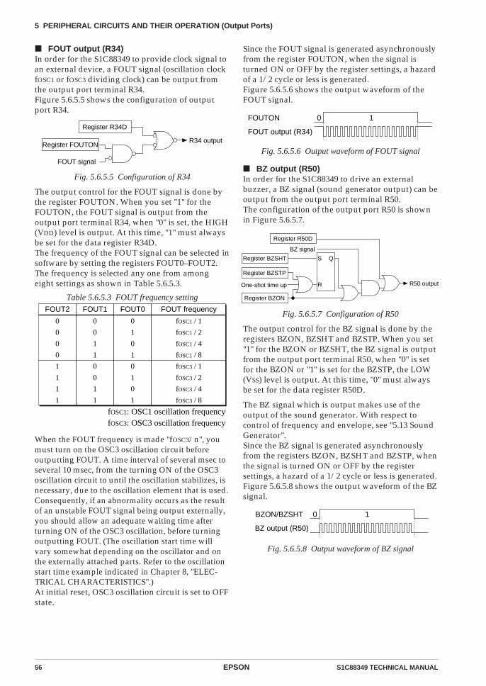
56 EPSON S1C88349 TECHNICAL MANUAL
5 PERIPHERAL CIRCUITS AND THEIR OPERATION (Output Ports)
FOUT output (R34)In order for the S1C88349 to provide clock signal toan external device, a FOUT signal (oscillation clockfOSC1 or fOSC3 dividing clock) can be output fromthe output port terminal R34.Figure 5.6.5.5 shows the configuration of outputport R34.
Since the FOUT signal is generated asynchronouslyfrom the register FOUTON, when the signal isturned ON or OFF by the register settings, a hazardof a 1/2 cycle or less is generated.Figure 5.6.5.6 shows the output waveform of theFOUT signal.
Register R34D
Register FOUTONR34 output
FOUT signal
Fig. 5.6.5.5 Configuration of R34
The output control for the FOUT signal is done bythe register FOUTON. When you set "1" for theFOUTON, the FOUT signal is output from theoutput port terminal R34, when "0" is set, the HIGH(VDD) level is output. At this time, "1" must alwaysbe set for the data register R34D.The frequency of the FOUT signal can be selected insoftware by setting the registers FOUT0–FOUT2.The frequency is selected any one from amongeight settings as shown in Table 5.6.5.3.
Table 5.6.5.3 FOUT frequency setting
When the FOUT frequency is made "fOSC3/n", youmust turn on the OSC3 oscillation circuit beforeoutputting FOUT. A time interval of several msec toseveral 10 msec, from the turning ON of the OSC3oscillation circuit to until the oscillation stabilizes, isnecessary, due to the oscillation element that is used.Consequently, if an abnormality occurs as the resultof an unstable FOUT signal being output externally,you should allow an adequate waiting time afterturning ON of the OSC3 oscillation, before turningoutputting FOUT. (The oscillation start time willvary somewhat depending on the oscillator and onthe externally attached parts. Refer to the oscillationstart time example indicated in Chapter 8, "ELEC-TRICAL CHARACTERISTICS".)At initial reset, OSC3 oscillation circuit is set to OFFstate.
FOUTON
FOUT output (R34)
0 1
Fig. 5.6.5.6 Output waveform of FOUT signal
BZ output (R50)In order for the S1C88349 to drive an externalbuzzer, a BZ signal (sound generator output) can beoutput from the output port terminal R50.The configuration of the output port R50 is shownin Figure 5.6.5.7.
BZON/BZSHT
BZ output (R50)
0 1
Fig. 5.6.5.7 Configuration of R50
The output control for the BZ signal is done by theregisters BZON, BZSHT and BZSTP. When you set"1" for the BZON or BZSHT, the BZ signal is outputfrom the output port terminal R50, when "0" is setfor the BZON or "1" is set for the BZSTP, the LOW(VSS) level is output. At this time, "0" must alwaysbe set for the data register R50D.
The BZ signal which is output makes use of theoutput of the sound generator. With respect tocontrol of frequency and envelope, see "5.13 SoundGenerator".Since the BZ signal is generated asynchronouslyfrom the registers BZON, BZSHT and BZSTP, whenthe signal is turned ON or OFF by the registersettings, a hazard of a 1/2 cycle or less is generated.Figure 5.6.5.8 shows the output waveform of the BZsignal.
Fig. 5.6.5.8 Output waveform of BZ signal
Register BZSTP
Register BZON
Register BZSHT
R
S Q
One-shot time up R50 output
BZ signal
Register R50D
FOUT2 FOUT frequency
0
0
0
0
1
1
1
1
fOSC1 / 1
fOSC1 / 2
fOSC1 / 4
fOSC1 / 8
fOSC3 / 1
fOSC3 / 2
fOSC3 / 4
fOSC3 / 8
FOUT1
0
0
1
1
0
0
1
1
FOUT0
0
1
0
1
0
1
0
1
fOSC1:fOSC3:
OSC1 oscillation frequencyOSC3 oscillation frequency
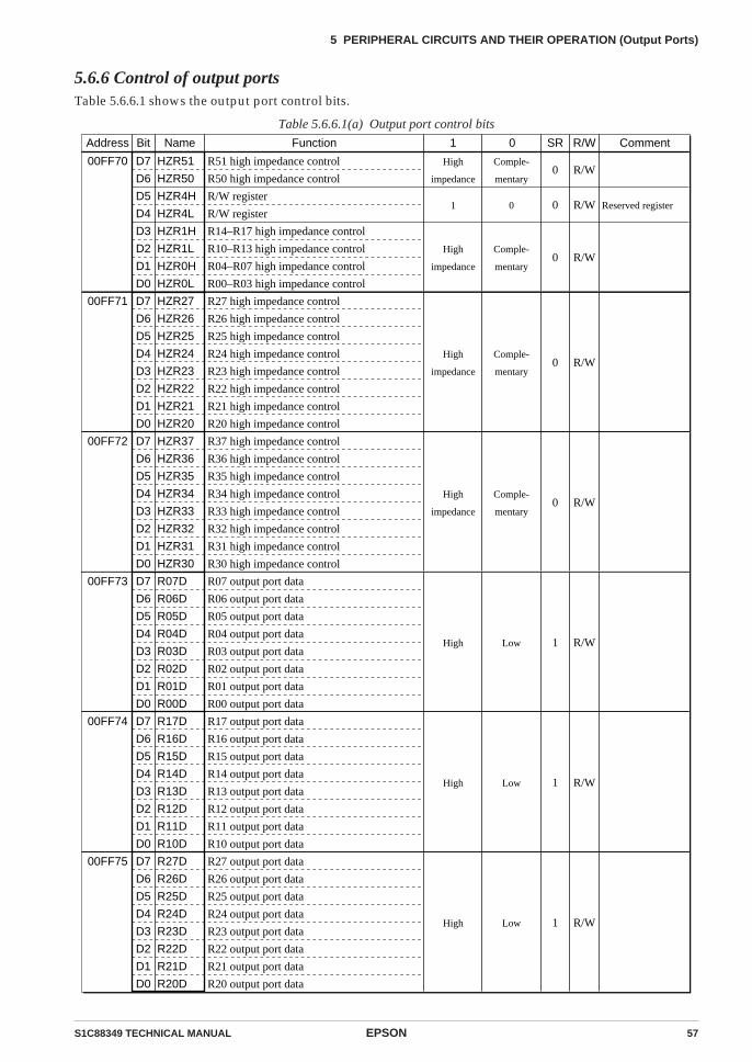
S1C88349 TECHNICAL MANUAL EPSON 57
5 PERIPHERAL CIRCUITS AND THEIR OPERATION (Output Ports)
5.6.6 Control of output portsTable 5.6.6.1 shows the output port control bits.
Table 5.6.6.1(a) Output port control bits
Address Bit Name
00FF70 D7
D6
D5
D4
D3
D2
D1
D0
HZR51
HZR50
HZR4H
HZR4L
HZR1H
HZR1L
HZR0H
HZR0L
SR R/WFunction Comment
R51 high impedance control
R50 high impedance control
R/W register
R/W register
R14–R17 high impedance control
R10–R13 high impedance control
R04–R07 high impedance control
R00–R03 high impedance control
Reserved register
1 0
0
0
0
R/W
R/W
R/W
High
impedance
1
High
impedance
Comple-
mentary
0
Comple-
mentary
00FF71 D7
D6
D5
D4
D3
D2
D1
D0
HZR27
HZR26
HZR25
HZR24
HZR23
HZR22
HZR21
HZR20
R27 high impedance control
R26 high impedance control
R25 high impedance control
R24 high impedance control
R23 high impedance control
R22 high impedance control
R21 high impedance control
R20 high impedance control
0 R/WHigh
impedance
Comple-
mentary
00FF72 D7
D6
D5
D4
D3
D2
D1
D0
HZR37
HZR36
HZR35
HZR34
HZR33
HZR32
HZR31
HZR30
R37 high impedance control
R36 high impedance control
R35 high impedance control
R34 high impedance control
R33 high impedance control
R32 high impedance control
R31 high impedance control
R30 high impedance control
0 R/WHigh
impedance
Comple-
mentary
00FF74 D7
D6
D5
D4
D3
D2
D1
D0
R17D
R16D
R15D
R14D
R13D
R12D
R11D
R10D
R17 output port data
R16 output port data
R15 output port data
R14 output port data
R13 output port data
R12 output port data
R11 output port data
R10 output port data
1 R/WHigh Low
00FF75 D7
D6
D5
D4
D3
D2
D1
D0
R27D
R26D
R25D
R24D
R23D
R22D
R21D
R20D
R27 output port data
R26 output port data
R25 output port data
R24 output port data
R23 output port data
R22 output port data
R21 output port data
R20 output port data
1 R/WHigh Low
00FF73 D7
D6
D5
D4
D3
D2
D1
D0
R07D
R06D
R05D
R04D
R03D
R02D
R01D
R00D
R07 output port data
R06 output port data
R05 output port data
R04 output port data
R03 output port data
R02 output port data
R01 output port data
R00 output port data
1 R/WHigh Low
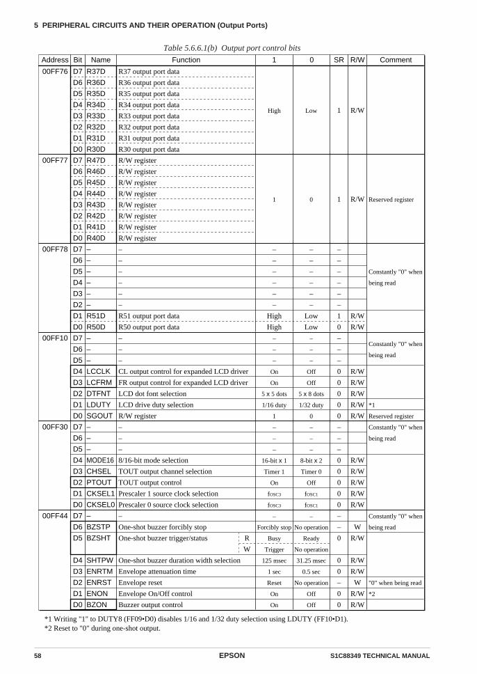
58 EPSON S1C88349 TECHNICAL MANUAL
5 PERIPHERAL CIRCUITS AND THEIR OPERATION (Output Ports)
Table 5.6.6.1(b) Output port control bits
Address Bit Name SR R/WFunction Comment1 0
00FF76 D7
D6
D5
D4
D3
D2
D1
D0
R37D
R36D
R35D
R34D
R33D
R32D
R31D
R30D
R37 output port data
R36 output port data
R35 output port data
R34 output port data
R33 output port data
R32 output port data
R31 output port data
R30 output port data
1 R/WHigh Low
00FF77 D7
D6
D5
D4
D3
D2
D1
D0
R47D
R46D
R45D
R44D
R43D
R42D
R41D
R40D
R/W register
R/W register
R/W register
R/W register
R/W register
R/W register
R/W register
R/W register
Reserved register1 R/W1 0
00FF78 D7
D6
D5
D4
D3
D2
D1
D0
–
–
–
–
–
–
R51D
R50D
–
–
–
–
–
–
R51 output port data
R50 output port data
Constantly "0" when
being read
–
–
–
–
–
–
1
0
R/W
R/W
00FF10 D7
D6
D5
D4
D3
D2
D1
D0
–
–
–
LCCLK
LCFRM
DTFNT
LDUTY
SGOUT
–
–
–
CL output control for expanded LCD driver
FR output control for expanded LCD driver
LCD dot font selection
LCD drive duty selection
R/W register
Constantly "0" when
being read
–
–
–
0
0
0
0
0
R/W
R/W
R/W
R/W
R/W
–
–
–
On
On
5 x 5 dots
1/16 duty
1
–
–
–
Off
Off
5 x 8 dots
1/32 duty
0
*1
Reserved register
00FF44 D7
D6
D5
D4
D3
D2
D1
D0
–
BZSTP
BZSHT
SHTPW
ENRTM
ENRST
ENON
BZON
–
One-shot buzzer forcibly stop
One-shot buzzer trigger/status
One-shot buzzer duration width selection
Envelope attenuation time
Envelope reset
Envelope On/Off control
Buzzer output control
Constantly "0" when
being read
"0" when being read
*2
–
–
0
0
0
–
0
0
W
R/W
R/W
R/W
W
R/W
R/W
–
Forcibly stop
Busy
Trigger
125 msec
1 sec
Reset
On
On
–
No operation
Ready
No operation
31.25 msec
0.5 sec
No operation
Off
Off
R
W
00FF30 D7
D6
D5
D4
D3
D2
D1
D0
–
–
–
MODE16
CHSEL
PTOUT
CKSEL1
CKSEL0
–
–
–
8/16-bit mode selection
TOUT output channel selection
TOUT output control
Prescaler 1 source clock selection
Prescaler 0 source clock selection
Constantly "0" when
being read
–
–
–
0
0
0
0
0
R/W
R/W
R/W
R/W
R/W
–
–
–
16-bit x 1
Timer 1
On
fOSC3
fOSC3
–
–
–
8-bit x 2
Timer 0
Off
fOSC1
fOSC1
*1 Writing "1" to DUTY8 (FF09•D0) disables 1/16 and 1/32 duty selection using LDUTY (FF10•D1).*2 Reset to "0" during one-shot output.
–
–
–
–
–
–
High
High
–
–
–
–
–
–
Low
Low
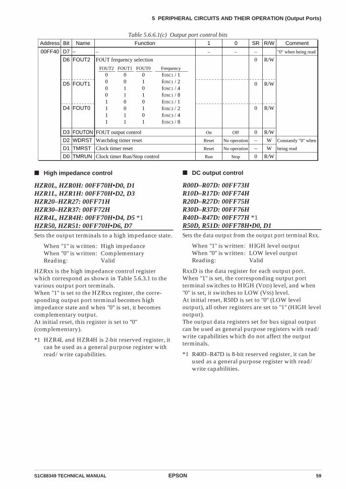
S1C88349 TECHNICAL MANUAL EPSON 59
5 PERIPHERAL CIRCUITS AND THEIR OPERATION (Output Ports)
Table 5.6.6.1(c) Output port control bits
High impedance control
HZR0L, HZR0H: 00FF70H•D0, D1HZR1L, HZR1H: 00FF70H•D2, D3HZR20–HZR27: 00FF71HHZR30–HZR37: 00FF72HHZR4L, HZR4H: 00FF70H•D4, D5 *1HZR50, HZR51: 00FF70H•D6, D7Sets the output terminals to a high impedance state.
When "1" is written: High impedanceWhen "0" is written: ComplementaryReading: Valid
HZRxx is the high impedance control registerwhich correspond as shown in Table 5.6.3.1 to thevarious output port terminals.When "1" is set to the HZRxx register, the corre-sponding output port terminal becomes highimpedance state and when "0" is set, it becomescomplementary output.At initial reset, this register is set to "0"(complementary).
*1 HZR4L and HZR4H is 2-bit reserved register, itcan be used as a general purpose register withread/write capabilities.
DC output control
R00D–R07D: 00FF73HR10D–R17D: 00FF74HR20D–R27D: 00FF75HR30D–R37D: 00FF76HR40D–R47D: 00FF77H *1R50D, R51D: 00FF78H•D0, D1Sets the data output from the output port terminal Rxx.
When "1" is written: HIGH level outputWhen "0" is written: LOW level outputReading: Valid
RxxD is the data register for each output port.When "1" is set, the corresponding output portterminal switches to HIGH (VDD) level, and when"0" is set, it switches to LOW (VSS) level.At initial reset, R50D is set to "0" (LOW leveloutput), all other registers are set to "1" (HIGH leveloutput).The output data registers set for bus signal outputcan be used as general purpose registers with read/write capabilities which do not affect the outputterminals.
*1 R40D–R47D is 8-bit reserved register, it can beused as a general purpose register with read/write capabilities.
Address Bit Name
00FF40 D7
D6
D5
D4
D3
D2
D1
D0
–
FOUT2
FOUT1
FOUT0
FOUTON
WDRST
TMRST
TMRUN
SR R/WFunction Comment
–
FOUT frequency selection
FOUT output control
Watchdog timer reset
Clock timer reset
Clock timer Run/Stop control
"0" when being read
Constantly "0" when
being read
1 0
–
0
0
0
0
–
–
0
R/W
R/W
R/W
R/W
W
W
R/W
–
On
Reset
Reset
Run
–
Off
No operation
No operation
Stop
FOUT2
00001111
FOUT1
00110011
FOUT0
01010101
Frequency
fOSC1 / 1fOSC1 / 2fOSC1 / 4fOSC1 / 8fOSC3 / 1fOSC3 / 2fOSC3 / 4fOSC3 / 8
60 EPSON S1C88349 TECHNICAL MANUAL
5 PERIPHERAL CIRCUITS AND THEIR OPERATION (Output Ports)
Special output control
LCCLK: 00FF10H•D4Controls the CL (LCD synchronous) signal output.
When "1" is written: CL signal outputWhen "0" is written: HIGH level (DC) outputReading: Valid
LCCLK is the output control register for CL signal.When "1" is set, the CL signal is output from theoutput port terminal R25 and when "0" is set, HIGH(VDD) level is output. At this time, "1" must alwaysbe set for the data register R25D.At initial reset, LCCLK is set to "0" (HIGH leveloutput).
LCFRM: 00FF10H•D3Controls the FR (LCD frame) signal output.
When "1" is written: FR signal outputWhen "0" is written: HIGH level (DC) outputReading: Valid
LCFRM is the output control register for FR signal.When "1" is set, the FR signal is output from theoutput port terminal R26 and when "0" is set, HIGH(VDD) level is output. At this time, "1" must alwaysbe set for the data register R26D.At initial reset, LCFRM is set to "0" (HIGH leveloutput).
PTOUT: 00FF30H•D2Controls the TOUT (programmable timer outputclock) signal output.
When "1" is written: TOUT signal outputWhen "0" is written: HIGH level (DC) outputReading: Valid
PTOUT is the output control register for TOUTsignal. When "1" is set, the TOUT signal is outputfrom the output port terminal R27 and when "0" isset, HIGH (VDD) level is output. At this time, "1"must always be set for the data register R27D.At initial reset, PTOUT is set to "0" (HIGH leveloutput).
FOUTON: 00FF40H•D3Controls the FOUT (fOSC1/fOSC3 dividing clock)signal output.
When "1" is written: FOUT signal outputWhen "0" is written: HIGH level (DC) outputReading: Valid
FOUTON is the output control register for FOUTsignal. When "1" is set, the FOUT signal is outputfrom the output port terminal R34 and when "0" isset, HIGH (VDD) level is output. At this time, "1"must always be set for the data register R34D.At initial reset, FOUTON is set to "0" (HIGH leveloutput).
FOUT0, FOUT1, FOUT2: 00FF40H•D4, D5, D6FOUT signal frequency is set as shown in Table5.6.6.2.
Table 5.6.6.2 FOUT frequency settings
At initial reset, this register is set to "0" (fOSC1/1).
BZON: 00FF44H•D0Controls the BZ (buzzer) signal output.
When "1" is written: BZ signal outputWhen "0" is written: LOW level (DC) outputReading: Valid
BZON is the output control register for BZ signal.When "1" is set, the BZ signal is output from theoutput port terminal R50 and when "0" is set, LOW(VSS) level is output. At this time, "0" must alwaysbe set for the data register R50D.At initial reset, BZON is set to "0" (LOW leveloutput).
FOUT2 FOUT frequency
0
0
0
0
1
1
1
1
fOSC1 / 1
fOSC1 / 2
fOSC1 / 4
fOSC1 / 8
fOSC3 / 1
fOSC3 / 2
fOSC3 / 4
fOSC3 / 8
FOUT1
0
0
1
1
0
0
1
1
FOUT0
0
1
0
1
0
1
0
1
fOSC1:fOSC3:
OSC1 oscillation frequencyOSC3 oscillation frequency
S1C88349 TECHNICAL MANUAL EPSON 61
5 PERIPHERAL CIRCUITS AND THEIR OPERATION (Output Ports)
BZSHT: 00FF45H•D5Controls the one-shot buzzer output.
When "1" is written: TriggerWhen "0" is written: No operation
When "1" is read: BusyWhen "0" is read: Ready
Writing "1" into BZSHT causes the one-shot outputcircuit to operate and the BZ signal to be output.The buzzer output is automatically turned OFFafter the time set by SHTPW has elapsed. At thistime, "0" must always be set for the data registerR50D.The one-shot output is only valid when the normalbuzzer output is OFF (BZON = "0") state. Thetrigger is invalid during ON (BZON = "1") state.When a re-trigger is assigned during a one-shotoutput, the one-shot output time set with SHTPW ismeasured again from that point. (time extension)The operation status of the one-shot output circuitcan be confirmed by reading BZSHT, when the one-shot output is ON, BZSHT reads "1" and when theoutput is OFF, it reads "0".At initial reset, BZSHT is set to "0" (ready).
BZSTP: 00FF45H•D6Forcibly stops the one-shot buzzer output.
When "1" is written: Forcibly stopWhen "0" is written: No operationReading: Constantly "0"
By writing "1" into BZSTP, the one-shot buzzeroutput can be stopped prior to the elapsing of thetime set with SHTPW.Writing "0" is invalid and writing "1" except duringone-shot output is also invalid.When "1" is written to BZSHT and BZSTP simulta-neously, BZSTP takes precedence and one-shotoutput becomes stop status.Since BZSTP is for writing only, during readout it isconstantly set to "0".
5.6.7 Programming notes(1) Since the special output signals (CL, FR, TOUT,
FOUT and BZ) are generated asynchronouslyfrom the output control registers (LCCLK,LCFRM, PTOUT, FOUTON, BZON, BZSHT andBZSTP), when the signals is turned ON or OFFby the output control register settings, a hazardof a 1/2 cycle or less is generated.
(2) When the FOUT frequency is made "fOSC3/n",you must turn on the OSC3 oscillation circuitbefore outputting FOUT. A time interval ofseveral msec to several 10 msec, from theturning ON of the OSC3 oscillation circuit tountil the oscillation stabilizes, is necessary, dueto the oscillation element that is used. Conse-quently, if an abnormality occurs as the result ofan unstable FOUT signal being output exter-nally, you should allow an adequate waitingtime after turning ON of the OSC3 oscillation,before turning outputting FOUT. (The oscilla-tion start time will vary somewhat dependingon the oscillator and on the externally attachedparts. Refer to the oscillation start time exampleindicated in Chapter 8, "ELECTRICAL CHAR-ACTERISTICS".)At initial reset, OSC3 oscillation circuit is set toOFF state.
(3) The SLP instruction has executed when thespecial output signals (TOUT, FOUT and BZ)are in the enable status, an unstable clock isoutput for the special output at the time ofreturn from the SLEEP state. Consequently,when shifting to the SLEEP state, you should setthe special output signal to the disable statusprior to executing the SLP instruction.
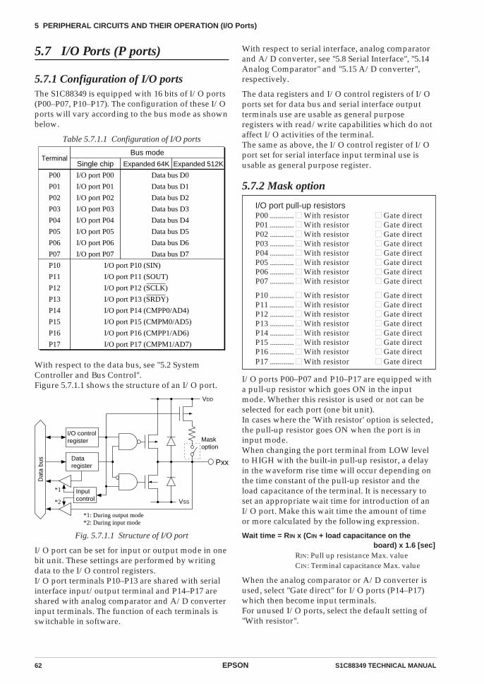
62 EPSON S1C88349 TECHNICAL MANUAL
5 PERIPHERAL CIRCUITS AND THEIR OPERATION (I/O Ports)
5.7 I/O Ports (P ports)
5.7.1 Configuration of I/O portsThe S1C88349 is equipped with 16 bits of I/O ports(P00–P07, P10–P17). The configuration of these I/Oports will vary according to the bus mode as shownbelow.
Table 5.7.1.1 Configuration of I/O ports
Terminal
P00
P01
P02
P03
P04
P05
P06
P07
P10
P11
P12
P13
P14
P15
P16
P17
I/O port P00
I/O port P01
I/O port P02
I/O port P03
I/O port P04
I/O port P05
I/O port P06
I/O port P07
Bus mode
Expanded 64K Expanded 512KSingle chip
Data bus D0
Data bus D1
Data bus D2
Data bus D3
Data bus D4
Data bus D5
Data bus D6
Data bus D7
I/O port P10 (SIN)
I/O port P11 (SOUT)
I/O port P12 (SCLK)
I/O port P13 (SRDY)
I/O port P14 (CMPP0/AD4)
I/O port P15 (CMPM0/AD5)
I/O port P16 (CMPP1/AD6)
I/O port P17 (CMPM1/AD7)
With respect to the data bus, see "5.2 SystemController and Bus Control".Figure 5.7.1.1 shows the structure of an I/O port.
Inputcontrol
VDD
VSS
Dat
a bu
s
PxxDataregister
I/O controlregister Mask
option
*1
*2
*1: During output mode*2: During input mode
Fig. 5.7.1.1 Structure of I/O port
I/O port can be set for input or output mode in onebit unit. These settings are performed by writingdata to the I/O control registers.I/O port terminals P10–P13 are shared with serialinterface input/output terminal and P14–P17 areshared with analog comparator and A/D converterinput terminals. The function of each terminals isswitchable in software.
With respect to serial interface, analog comparatorand A/D converter, see "5.8 Serial Interface", "5.14Analog Comparator" and "5.15 A/D converter",respectively.
The data registers and I/O control registers of I/Oports set for data bus and serial interface outputterminals use are usable as general purposeregisters with read/write capabilities which do notaffect I/O activities of the terminal.The same as above, the I/O control register of I/Oport set for serial interface input terminal use isusable as general purpose register.
5.7.2 Mask option
I/O port pull-up resistorsP00 ............ With resistor Gate directP01 ............ With resistor Gate directP02 ............ With resistor Gate directP03 ............ With resistor Gate directP04 ............ With resistor Gate directP05 ............ With resistor Gate directP06 ............ With resistor Gate directP07 ............ With resistor Gate direct
P10 ............ With resistor Gate directP11 ............ With resistor Gate directP12 ............ With resistor Gate directP13 ............ With resistor Gate directP14 ............ With resistor Gate directP15 ............ With resistor Gate directP16 ............ With resistor Gate directP17 ............ With resistor Gate direct
I/O ports P00–P07 and P10–P17 are equipped witha pull-up resistor which goes ON in the inputmode. Whether this resistor is used or not can beselected for each port (one bit unit).In cases where the 'With resistor' option is selected,the pull-up resistor goes ON when the port is ininput mode.When changing the port terminal from LOW levelto HIGH with the built-in pull-up resistor, a delayin the waveform rise time will occur depending onthe time constant of the pull-up resistor and theload capacitance of the terminal. It is necessary toset an appropriate wait time for introduction of anI/O port. Make this wait time the amount of timeor more calculated by the following expression.
Wait time = RIN x (CIN + load capacitance on the board) x 1.6 [sec]
RIN: Pull up resistance Max. valueCIN: Terminal capacitance Max. value
When the analog comparator or A/D converter isused, select "Gate direct" for I/O ports (P14–P17)which then become input terminals.For unused I/O ports, select the default setting of"With resistor".

S1C88349 TECHNICAL MANUAL EPSON 63
5 PERIPHERAL CIRCUITS AND THEIR OPERATION (I/O Ports)
5.7.3 I/O control registers and I/O modeI/O ports P00–P07 and P10–P17 are set either toinput or output modes by writing data to the I/Ocontrol registers IOC00–IOC07 and IOC10–IOC17which correspond to each bit.To set an I/O port to input mode, write "0" to the I/Ocontrol register.An I/O port which is set to input mode will shift to ahigh impedance state and functions as an input port.Readout in input mode consists simply of a directreadout of the input terminal state: the data being "1"when the input terminal is at HIGH (VDD) level and"0" when it is at LOW (VSS) level.When the "With resistor" option is selected usingthe mask option, the resistor is pulled up onto theport terminal in input mode.
Even in input mode, data can be written to the dataregisters without affecting the terminal state.To set an I/O port to output mode, write "1" to theI/O control register. An I/O port which is set tooutput mode functions as an output port.When port output data is "1", a HIGH (VDD) level isoutput and when it is "0", a LOW (VSS) level isoutput. Readout in output mode consists of thecontents of the data register.At initial reset, I/O control registers are set to "0"(I/O ports are set to input mode).
5.7.4 Control of I/O portsTable 5.7.4.1 shows the I/O port control bits.
Table 5.7.4.1 I/O port control bitsAddress Bit Name
00FF61 D7
D6
D5
D4
D3
D2
D1
D0
IOC17
IOC16
IOC15
IOC14
IOC13
IOC12
IOC11
IOC10
SR R/WFunction Comment
P17 I/O control register
P16 I/O control register
P15 I/O control register
P14 I/O control register
P13 I/O control register
P12 I/O control register
P11 I/O control register
P10 I/O control register
1 0
0 R/WOutput Input
00FF62 D7
D6
D5
D4
D3
D2
D1
D0
P07D
P06D
P05D
P04D
P03D
P02D
P01D
P00D
P07 I/O port data
P06 I/O port data
P05 I/O port data
P04 I/O port data
P03 I/O port data
P02 I/O port data
P01 I/O port data
P00 I/O port data
1 R/WHigh Low
00FF63 D7
D6
D5
D4
D3
D2
D1
D0
P17D
P16D
P15D
P14D
P13D
P12D
P11D
P10D
P17 I/O port data
P16 I/O port data
P15 I/O port data
P14 I/O port data
P13 I/O port data
P12 I/O port data
P11 I/O port data
P10 I/O port data
1 R/WHigh Low
00FF60 D7
D6
D5
D4
D3
D2
D1
D0
IOC07
IOC06
IOC05
IOC04
IOC03
IOC02
IOC01
IOC00
P07 I/O control register
P06 I/O control register
P05 I/O control register
P04 I/O control register
P03 I/O control register
P02 I/O control register
P01 I/O control register
P00 I/O control register
0 R/WOutput Input
64 EPSON S1C88349 TECHNICAL MANUAL
5 PERIPHERAL CIRCUITS AND THEIR OPERATION (I/O Ports)
P00D–P07D: 00FF62HP10D–P17D: 00FF63HHow I/O port terminal Pxx data readout andoutput data settings are performed.
When writing data:
When "1" is written: HIGH levelWhen "0" is written: LOW level
When the I/O port is set to output mode, the datawritten is output as is to the I/O port terminal. Interms of port data, when "1" is written, the portterminal goes to HIGH (VDD) level and when "0" iswritten to a LOW (VSS) level.Even when the port is in input mode, data can stillbe written in.
When reading out data:
When "1" is read: HIGH level ("1")When "0" is read: LOW level ("0")
When an I/O port is in input mode, the voltagelevel being input to the port terminal is read out.When terminal voltage is HIGH (VDD), it is read asa "1", and when it is LOW (VSS), it is read as a "0".Furthermore, in output mode, the contents of thedata register are read out.At initial reset, this register is set to "1" (HIGHlevel).
Note: The data registers of I/O ports set for thedata bus and output terminal of serialinterface can be used as general purposeregisters with read/write capabilities whichdo not affect I/O activities of the terminals.
IOC00–IOC07: 00FF60HIOC10–IOC17: 00FF61HSets the I/O ports to input or output mode.
When "1" is written: Output modeWhen "0" is written: Input modeReading: Valid
IOCxx is the I/O control register which correspondto each I/O port in a bit unit.Writing "1" to the IOCxx register will switch thecorresponding I/O port Pxx to output mode, andwriting "0" will switch it to input mode.When the analog comparator or A/D converter isused, "0" must always be set for the I/O controlregisters (IOC14–IOC17) of I/O ports which willbecome input terminals.At initial reset, this register is set to "0" (inputmode).
Note: The data registers of I/O ports set for thedata bus and input terminal of serial inter-face can be used as general purposeregisters with read/write capabilities whichdo not affect I/O activities of the terminals.
5.7.5 Programming notes(1) When changing the port terminal from LOW
level to HIGH with the built-in pull-up resistor,a delay in the waveform rise time will occurdepending on the time constant of the pull-upresistor and the load capacitance of the termi-nal. It is necessary to set an appropriate waittime for introduction of an I/O port. Make thiswait time the amount of time or more calculatedby the following expression.
Wait time = RIN x (CIN + load capacitance on the board) x 1.6 [sec]
RIN: Pull up resistance Max. valueCIN: Terminal capacitance Max. value
(2) When the analog comparator or A/D converteris used, "0" must always be set for the I/Ocontrol registers (IOC14–IOC17) of I/O portswhich will become input terminals.
S1C88349 TECHNICAL MANUAL EPSON 65
5 PERIPHERAL CIRCUITS AND THEIR OPERATION (Serial Interface)
5.8 Serial Interface
5.8.1 Configuration of serial interfaceThe S1C88349 incorporates a full duplex serialinterface (when asynchronous system is selected)that allows the user to select either clock synchro-nous system or asynchronous system.The data transfer method can be selected in soft-ware.When the clock synchronous system is selected, 8-bit data transfer is possible.When the asynchronous system is selected, either 7-bit or 8-bit data transfer is possible, and a paritycheck of received data and the addition of a paritybit for transmitting data can automatically be doneby selecting in software.Figure 5.8.1.1 shows the configuration of the serialinterface.
Serial interface input/output terminals, SIN, SOUT,SCLK and SRDY are shared with I/O ports P10–P13.In order to utilize these terminals for the serialinterface input/output terminals, proper settingshave to be made with registers ESIF, SMD0 andSMD1. (At initial reset, these terminals are set as I/Oport terminals.)The direction of I/O port terminals set for serialinterface input/output terminals are determined bythe signal and transfer mode for each terminal.Furthermore, the settings for the corresponding I/Ocontrol registers for the I/O ports become invalid.
SIN and SOUT are serial data input and outputterminals which function identically in clocksynchronous system and asynchronous system.SCLK is exclusively for use with clock synchronoussystem and functions as a synchronous clock input/output terminal. SRDY is exclusively for use in clocksynchronous slave mode and functions as a send-receive ready signal output terminal.When asynchronous system is selected, since SCLKand SRDY are superfluous, the I/O port terminalsP12 and P13 can be used as I/O ports.In the same way, when clock synchronous mastermode is selected, since SRDY is superfluous, the I/Oport terminal P13 can be used as I/O port.
Table 5.8.1.1 Configuration of input/output terminals
Terminal When serial interface is selected
P10
P11
P12
P13
SIN
SOUT
SCLK
SRDY
* The terminals used may vary depending on the transfer mode.
fOSC3
Data bus
SOUT(P11)
Serial I/O control& status register
Receiveddata buffer
Interruptcontrol circuit
Serial inputcontrol circuit
Received datashift register
Transmitting datashift register
Serial outputcontrol circuitSIN(P10)
Clockcontrol circuit
READY outputcontrol circuit
SCLK(P12)
Error detectioncircuit
SRDY(P13)Start bitdetection circuit
Programmable timer 1 underflow signal
Interruptrequest
OSC3 oscillation circuit
Fig. 5.8.1.1 Configuration of serial interface

66 EPSON S1C88349 TECHNICAL MANUAL
5 PERIPHERAL CIRCUITS AND THEIR OPERATION (Serial Interface)
5.8.2 Mask optionSince serial interface input/output terminals areshared with the I/O ports, serial interface terminalspecifications have necessarily been selected withthe mask option for I/O ports.
I/O port pull-up resistorsP10 (SIN) ........ With resistor Gate directP12 (SCLK) .... With resistor Gate direct
Each I/O port terminal is equipped with a pull-upresistor which goes ON in input mode. A selectioncan be made for each port (one bit unit) as towhether or not the resistor will be used.Specifications (whether the pull-up will be used ornot) of P10 (SIN) and P12 (SCLK) which will becomeinput terminals when using the serial interface aredecided by settings the options for the I/O port.
When "Gate direct" is selected in the serial I/Fmode, be sure that the input terminals do not gointo a floating state.
5.8.3 Transfer modesThere are four transfer modes for the serial inter-face and mode selection is made by setting the twobits of the mode selection registers SMD0 andSMD1 as shown in the table below.
Table 5.8.3.1 Transfer modes
At initial reset, transfer mode is set to clock syn-chronous master mode.
Clock synchronous master modeIn this mode, the internal clock is utilized as asynchronous clock for the built-in shift registers,and clock synchronous 8-bit serial transfers can beperformed with this serial interface as the master.The synchronous clock is also output from theSCLK terminal which enables control of theexternal (slave side) serial I/O device. Since theSRDY terminal is not utilized in this mode, it can beused as an I/O port.Figure 5.8.3.1(a) shows the connection example ofinput/output terminals in the clock synchronousmaster mode.
Table 5.8.3.2 Terminal settings corresponding to each transfer mode
Mode SIN
Asynchronous 8-bit
Asynchronous 7-bit
Clock synchronous slave
Clock synchronous master
P13
P13
Output
P13
SOUT SCLK SRDY
P12
P12
Input
Output
Output
Output
Output
Output
Input
Input
Input
Input
Clock synchronous slave modeIn this mode, a synchronous clock from the external(master side) serial input/output device is utilizedand clock synchronous 8-bit serial transfers can beperformed with this serial interface as the slave.The synchronous clock is input to the SCLKterminal and is utilized by this interface as thesynchronous clock.Furthermore, the SRDY signal indicating thetransmit-receive ready status is output from theSRDY terminal in accordance with the serialinterface operating status.In the slave mode, the settings for registers SCS0and SCS1 used to select the clock source are invalid.Figure 5.8.3.1(b) shows the connection example ofinput/output terminals in the clock synchronousslave mode.
Asynchronous 7-bit modeIn this mode, asynchronous 7-bit transfer can beperformed. Parity check during data reception andaddition of parity bit (odd/even/none) duringtransmitting can be specified and data processed in7 bits with or without parity. Since this modeemploys the internal clock, the SCLK terminal isnot used. Furthermore, since the SRDY terminal isnot utilized either, both of these terminals can beused as I/O ports.Figure 5.8.3.1(c) shows the connection example ofinput/output terminals in the asynchronous mode.
Asynchronous 8-bit modeIn this mode, asynchronous 8-bit transfer can beperformed. Parity check during data reception andaddition of parity bit (odd/even/none) duringtransmitting can be specified and data processed in8 bits with or without parity. Since this modeemploys the internal clock, the SCLK terminal isnot used. Furthermore, since the SRDY terminal isnot utilized either, both of these terminals can beused as I/O ports.Figure 5.8.3.1(c) shows the connection example ofinput/output terminals in the asynchronous mode.
SMD1 SMD0 Mode
1
1
0
0
1
0
1
0
Asynchronous 8-bit
Asynchronous 7-bit
Clock synchronous slave
Clock synchronous master
S1C88349 TECHNICAL MANUAL EPSON 67
5 PERIPHERAL CIRCUITS AND THEIR OPERATION (Serial Interface)
This register setting is invalid in clock synchronousslave mode and the external clock input from theSCLK terminal is used.When the "programmable timer" is selected, theprogrammable timer 1 underflow signal is dividedby 1/2 and this signal used as the clock source.With respect to the transfer rate setting, see "5.11Programmable Timer".At initial reset, the synchronous clock is set to"fOSC3/16".Whichever clock is selected, the signal is furtherdivided by 1/16 and then used as the synchronousclock.Furthermore, external clock input is used as is forSCLK in clock synchronous slave mode.Table 5.8.4.2 shows an examples of transfer rates andOSC3 oscillation frequencies when the clock sourceis set to programmable timer.When the demultiplied signal of the OSC3 oscilla-tion circuit is made the clock source, it is necessaryto turn the OSC3 oscillation ON, prior to using theserial interface.A time interval of several msec to several 10 msec,from the turning ON of the OSC3 oscillation circuitto until the oscillation stabilizes, is necessary, due tothe oscillation element that is used. Consequently,you should allow an adequate waiting time afterturning ON of the OSC3 oscillation, before startingtransmitting/receiving of serial interface. (Theoscillation start time will vary somewhat dependingon the oscillator and on the externally attached parts.Refer to the oscillation start time example indicatedin Chapter 8, "ELECTRICAL CHARACTERISTICS".)At initial reset, the OSC3 oscillation circuit is set toOFF status.
Transfer rate
(bps)
9,600
4,800
2,400
1,200
600
300
150
OSC3 oscillation frequency / Programmable timer settings
fOSC3 = 3.072 MHz
PSC1X
0 (1/1)
0 (1/1)
0 (1/1)
0 (1/1)
0 (1/1)
1 (1/4)
1 (1/4)
RLD1X
09H
13H
27H
4FH
9FH
4FH
9FH
fOSC3 = 4.608 MHz
PSC1X
0 (1/1)
0 (1/1)
0 (1/1)
0 (1/1)
0 (1/1)
1 (1/4)
1 (1/4)
RLD1X
0EH
1DH
3BH
77H
EFH
77H
EFH
fOSC3 = 4.9152 MHz
PSC1X
0 (1/1)
0 (1/1)
0 (1/1)
0 (1/1)
0 (1/1)
1 (1/4)
1 (1/4)
RLD1X
0FH
1FH
3FH
7FH
FFH
7FH
FFH
Table 5.8.4.2OSC3 oscillation frequencies and
transfer rates
Data input
Data output
CLOCK output
READY input
SIN(P10)
SOUT(P11)
SCLK(P12)
SRDY(P13)
Externalserial device
S1C88349
Data input
Data output
CLOCK input
READY output
SIN(P10)
SOUT(P11)
SCLK(P12)
Input port(Kxx)
Externalserial device
S1C88349
(a) Clock synchronous master mode
(b) Clock synchronous slave mode
(c) Asynchronous 7-bit/8-bit mode
Fig. 5.8.3.1 Connection examples of serial interface I/O terminals
5.8.4 Clock sourceThere are four clock sources and selection is madeby setting the two bits of the clock source selectionregister SCS0 and SCS1 as shown in table below.
Table 5.8.4.1 Clock source
SCS1
1
1
0
0
SCS0
1
0
1
0
Clock source
Programmable timer
fOSC3 / 4
fOSC3 / 8
fOSC3 / 16
Data input
Data output
SIN(P10)
SOUT(P11)
Externalserial device
S1C88349
fOSC31/41/81/16
1/16Synchro-nous clock
Programmable timer 1underflow signal
SCLK(Clock synchronous slave mode)
Divider Selector Selector
1/2
OSC3oscillationcircuit
Fig. 5.8.4.1Division of the synchronous clock
68 EPSON S1C88349 TECHNICAL MANUAL
5 PERIPHERAL CIRCUITS AND THEIR OPERATION (Serial Interface)
5.8.5 Transmit-receive controlBelow is a description of the registers which handletransmit-receive control. With respect to transmit-receive control procedures and operations, pleaserefer to the following sections in which these arediscussed on a mode by mode basis.
Shift register and received data bufferExclusive shift registers for transmitting andreceiving are installed in this serial interface.Consequently, duplex communication simultane-ous transmit and receive is possible when theasynchronous system is selected.
Data being transmitted are written to TRXD0–TRXD7 and converted to serial through the shiftregister and is output from the SOUT terminal.
In the reception section, a received data buffer isinstalled separate from the shift register.Data being received are input to the SIN terminaland is converted to parallel through the shiftregister and written to the received data buffer.Since the received data buffer can be read evenduring serial input operation, the continuous datais received efficiently.However, since buffer functions are not used inclock synchronous mode, be sure to read out databefore the next data reception begins.
Transmit enable register and transmitcontrol bit
For transmitting control, use the transmit enableregister TXEN and transmit control bit TXTRG.
The transmit enable register TXEN is used to set thetransmitting enable/disable status. When "1" iswritten to this register to set the transmitting enablestatus, clock input to the shift register is enabledand the system is ready to transmit data. In theclock synchronous mode, synchronous clock input/output from the SCLK terminal is also enabled.
The transmit control bit TXTRG is used as thetrigger to start transmitting data.Data to be transmitted is written to the transmitdata shift register, and when transmitting prepara-tions a recomplete, "1" is written to TXTRG where-upon data transmitting begins.When interrupt has been enabled, an interrupt isgenerated when the transmission is completed. Ifthere is subsequent data to be transmitted it can besent using this interrupt.
In addition, TXTRG can be read as the status. Whenset to "1", it indicates transmitting operation, and"0" indicates transmitting stop.For details on timing, see the timing chart whichgives the timing for each mode.
When not transmitting, set TXEN to "0" to disabletransmitting status.
Receive enable register, receive control bitFor receiving control, use the receive enable registerRXEN and receive control bit RXTRG.Receive enable register RXEN is used to set receiv-ing enable/disable status. When "1" is written intothis register to set the receiving enable status, clockinput to the shift register is enabled and the systemis ready to receive data. In the clock synchronousmode, synchronous clock input/output from theSCLK terminal is also enabled.With the above setting, receiving begins and serialdata input from the SIN terminal goes to the shiftregister.The operation of the receive control bit RXTRG isslightly different depending on whether a clocksynchronous system or an asynchronous system isbeing used.In the clock synchronous system, the receivecontrol bit RXTRG is used as the trigger to startreceiving data.When received data has been read and the prepara-tion for next data receiving is completed, write "1"into RXTRG to start receiving. (When "1" is writtento RXTRG in slave mode, SRDY switches to "0".)In an asynchronous system, RXTRG is used toprepare for next data receiving. After reading thereceived data from the received data buffer, write"1" into RXTRG to signify that the received databuffer is empty. If "1" is not written into RXTRG,the overrun error flag OER will be set to "1" whenthe next receiving operation is completed. (Anoverrun error will be generated when receiving iscompleted between reading the received data andthe writing of "1" to RXTRG.)In addition, RXTRG can be read as the status. Ineither clock synchronous mode or asynchronousmode, when RXTRG is set to "1", it indicatesreceiving operation and when set to "0", it indicatesthat receiving has stopped.For details on timing, see the timing chart whichgives the timing for each mode.
When you do not receive, set RXEN to "0" to disablereceiving status.

S1C88349 TECHNICAL MANUAL EPSON 69
5 PERIPHERAL CIRCUITS AND THEIR OPERATION (Serial Interface)
(2) Port selectionBecause serial interface input/output ports SIN,SOUT, SCLK and SRDY are set as I/O portterminals P10–P13 at initial reset, "1" must bewritten to the serial interface enable registerESIF in order to set these terminals for serialinterface use.
(3) Setting of transfer modeSelect the clock synchronous mode by writingthe data as indicated below to the two bits of themode selection registers SMD0 and SMD1.
Master mode: SMD0 = "0", SMD1 = "0"Slave mode: SMD0 = "1", SMD1 = "0"
(4) Clock source selectionIn the master mode, select the synchronousclock source by writing data to the two bits ofthe clock source selection registers SCS0 andSCS1. (See Table 5.8.4.1.)This selection is not necessary in the slavemode.
Since all the registers mentioned in (2)–(4) areassigned to the same address, it's possible to setthem all with one instruction. The parity enableregister EPR is also assigned to this address,however, since parity is not necessary in theclock synchronous mode, parity check will nottake place regardless of how they are set.
(5) Clock source controlWhen the master mode is selected and pro-grammable timer for the clock source is se-lected, set transfer rate on the programmabletimer side. (See "5.11 Programmable Timer".)When the divided signal of OSC3 oscillationcircuit is selected for the clock source, be surethat the OSC3 oscillation circuit is turned ONprior to commencing data transfer. (See "5.4Oscillation Circuits and Operating Mode".)
SCLK
Data D0 D1 D2 D3 D4 D5 D6 D7LSB MSB
Fig. 5.8.6.1 Transfer data configuration using clock synchronous mode
Below is a description of initialization whenperforming clock synchronous transfer, transmit-receive control procedures and operations.With respect to serial interface interrupt, see "5.8.8Interrupt function".
Initialization of serial interfaceWhen performing clock synchronous transfer, thefollowing initial settings must be made.
(1) Setting of transmitting/receiving disableTo set the serial interface into a status in whichboth transmitting and receiving are disabled, "0"must be written to both the transmit enableregister TXEN and the receive enable registerRXEN. Fix these two registers to a disable statusuntil data transfer actually begins.
5.8.6 Operation ofclock synchronous transfer
Clock synchronous transfer involves the transfer of8-bit data by synchronizing it to eight clocks. Thesame synchronous clock is used by both thetransmitting and receiving sides.When the serial interface is used in the mastermode, the clock signal selected using SCS0 andSCS1 is further divided by 1/16 and employed asthe synchronous clock. This signal is then sent viathe SCLK terminal to the slave side (external serialI/O device).When used in the slave mode, the clock input to theSCLK terminal from the master side (external serialinput/output device) is used as the synchronousclock.
In the clock synchronous mode, since one clock line(SCLK) is shared for both transmitting and receiv-ing, transmitting and receiving cannot be per-formed simultaneously. (Half duplex only ispossible in clock synchronous mode.)
Transfer data is fixed at 8 bits and both transmittingand receiving are conducted with the LSB (bit 0)coming first.
70 EPSON S1C88349 TECHNICAL MANUAL
5 PERIPHERAL CIRCUITS AND THEIR OPERATION (Serial Interface)
Data transmit procedureThe control procedure and operation duringtransmitting is as follows.
(1) Write "0" in the transmit enable register TXENand the receive enable register RXEN to resetthe serial interface.
(2) Write "1" in the transmit enable register TXENto set into the transmitting enable status.
(3) Write the transmitting data into TRXD0–TRXD7.
(4) In case of the master mode, confirm the receiveready status on the slave side (external serialinput/output device), if necessary. Wait until itreaches the receive ready status.
(5) Write "1" in the transmit control bit TXTRG andstart transmitting.
In the master mode, this control causes thesynchronous clock to change to enable and to beprovided to the shift register for transmittingand output from the SCLK terminal.In the slave mode, it waits for the synchronousclock to be input from the SCLK terminal.The transmitting data of the shift register shiftsone bit at a time at each falling edge of thesynchronous clock and is output from the SOUTterminal. When the final bit (MSB) is output, theSOUT terminal is maintained at that level, untilthe next transmitting begins.
The transmitting complete interrupt factor flagFSTRA is set to "1" at the point where the datatransmitting of the shift register is completed.When interrupt has been enabled, a transmit-ting complete interrupt is generated at thispoint.Set the following transmitting data using thisinterrupt.
(6) Repeat steps (3) to (5) for the number of bytes oftransmitting data, and then set the transmitdisable status by writing "0" to the transmitenable register TXEN, when the transmitting iscompleted.
Data transmitting
End
TXEN ← 0, RXEN ← 0
No
Yes
Transmit complete ?
Set transmitting data
to TRXD0–TRXD7
No
Yes
FSTRA = 1 ?
TXEN ← 0
TXTRG ← 1
TXEN ← 1
No
Yes
Receiver ready ?In case of master mode
Fig. 5.8.6.2 Transmit procedure in clock synchronous mode
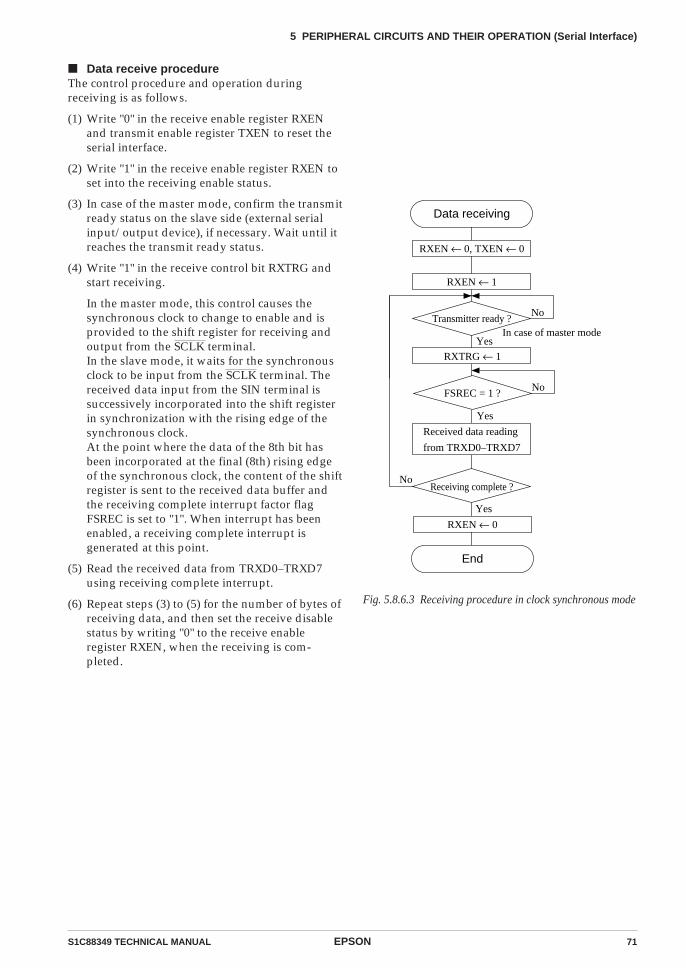
S1C88349 TECHNICAL MANUAL EPSON 71
5 PERIPHERAL CIRCUITS AND THEIR OPERATION (Serial Interface)
Data receive procedureThe control procedure and operation duringreceiving is as follows.
(1) Write "0" in the receive enable register RXENand transmit enable register TXEN to reset theserial interface.
(2) Write "1" in the receive enable register RXEN toset into the receiving enable status.
(3) In case of the master mode, confirm the transmitready status on the slave side (external serialinput/output device), if necessary. Wait until itreaches the transmit ready status.
(4) Write "1" in the receive control bit RXTRG andstart receiving.
In the master mode, this control causes thesynchronous clock to change to enable and isprovided to the shift register for receiving andoutput from the SCLK terminal.In the slave mode, it waits for the synchronousclock to be input from the SCLK terminal. Thereceived data input from the SIN terminal issuccessively incorporated into the shift registerin synchronization with the rising edge of thesynchronous clock.At the point where the data of the 8th bit hasbeen incorporated at the final (8th) rising edgeof the synchronous clock, the content of the shiftregister is sent to the received data buffer andthe receiving complete interrupt factor flagFSREC is set to "1". When interrupt has beenenabled, a receiving complete interrupt isgenerated at this point.
(5) Read the received data from TRXD0–TRXD7using receiving complete interrupt.
(6) Repeat steps (3) to (5) for the number of bytes ofreceiving data, and then set the receive disablestatus by writing "0" to the receive enableregister RXEN, when the receiving is com-pleted.
Data receiving
End
RXEN ← 0, TXEN ← 0
No
Yes
Receiving complete ?
Received data reading
from TRXD0–TRXD7
No
Yes
FSREC = 1 ?
RXEN ← 0
RXTRG ← 1
RXEN ← 1
No
Yes
Transmitter ready ?In case of master mode
Fig. 5.8.6.3 Receiving procedure in clock synchronous mode
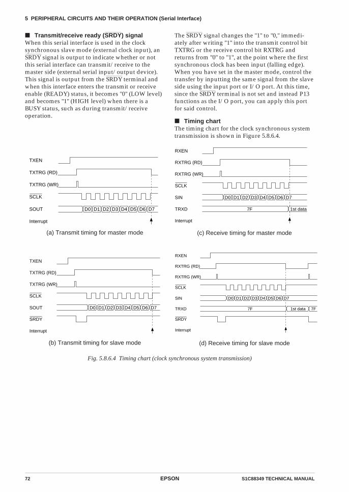
72 EPSON S1C88349 TECHNICAL MANUAL
5 PERIPHERAL CIRCUITS AND THEIR OPERATION (Serial Interface)
The SRDY signal changes the "1" to "0," immedi-ately after writing "1" into the transmit control bitTXTRG or the receive control bit RXTRG andreturns from "0" to "1", at the point where the firstsynchronous clock has been input (falling edge).When you have set in the master mode, control thetransfer by inputting the same signal from the slaveside using the input port or I/O port. At this time,since the SRDY terminal is not set and instead P13functions as the I/O port, you can apply this portfor said control.
Timing chartThe timing chart for the clock synchronous systemtransmission is shown in Figure 5.8.6.4.
(a) Transmit timing for master mode
(b) Transmit timing for slave mode
(c) Receive timing for master mode
(d) Receive timing for slave mode
Fig. 5.8.6.4 Timing chart (clock synchronous system transmission)
Transmit/receive ready (SRDY) signalWhen this serial interface is used in the clocksynchronous slave mode (external clock input), anSRDY signal is output to indicate whether or notthis serial interface can transmit/receive to themaster side (external serial input/output device).This signal is output from the SRDY terminal andwhen this interface enters the transmit or receiveenable (READY) status, it becomes "0" (LOW level)and becomes "1" (HIGH level) when there is aBUSY status, such as during transmit/receiveoperation.
SCLK
TXTRG (RD)
SOUT D0 D1 D2 D3 D4 D5 D6 D7
TXEN
Interrupt
TXTRG (WR)
SCLK
TXTRG (RD)
SOUT D0 D1 D2 D3 D4 D5 D6 D7
TXEN
Interrupt
TXTRG (WR)
SRDY
SCLK
RXTRG (RD)
SIN D0 D1 D2 D3 D4 D5 D6 D7
RXEN
Interrupt
RXTRG (WR)
TRXD 7F 1st data
SRDY
7F
SCLK
RXTRG (RD)
SIN D0 D1 D2 D3 D4 D5 D6 D7
RXEN
Interrupt
RXTRG (WR)
TRXD 7F 1st data

S1C88349 TECHNICAL MANUAL EPSON 73
5 PERIPHERAL CIRCUITS AND THEIR OPERATION (Serial Interface)
5.8.7 Operation of asynchronous transferAsynchronous transfer is a mode that transfers byadding a start bit and a stop bit to the front and theback of each piece of serial converted data. In thismode, there is no need to use a clock that is fullysynchronized clock on the transmit side and thereceive side, but rather transmission is done whileadopting the synchronization at the start/stop bitsthat have attached before and after each piece ofdata. The RS-232C interface functions can be easilyrealized by selecting this transfer mode.This interface has separate transmit and receiveshift registers and is designed to permit full duplextransmission to be done simultaneously for trans-mitting and receiving.
For transfer data in the asynchronous 7-bit mode,either 7 bits data (no parity) or 7 bits data + paritybit can be selected. In the asynchronous 8-bit mode,either 8 bits data (no parity) or 8 bits data + paritybit can be selected.Parity can be even or odd, and parity checking ofreceived data and adding a party bit to transmittingdata will be done automatically. Thereafter, it is notnecessary to be conscious of parity itself in theprogram.The start bit and stop bit are respectively fixed atone bit and data is transmitted and received byplacing the LSB (bit 0) at the front.
Initialization of serial interfaceThe below initialization must be done in cases ofasynchronous system transfer.
(1) Setting of transmitting/receiving disableTo set the serial interface into a status in whichboth transmitting and receiving are disabled, "0"must be written to both the transmit enableregister TXEN and the receive enable registerRXEN. Fix these two registers to a disable statusuntil data transfer actually begins.
(2) Port selectionBecause serial interface input/output terminalsSIN and SOUT are set as I/O port terminals P10and P11 at initial reset, "1" must be written tothe serial interface enable register ESIF in orderto set these terminals for serial interface use.SCLK and SRDY terminals set in the clocksynchronous mode are not used in the asynchro-nous mode. These terminals function as I/Oport terminals P12 and P13.
(3) Setting of transfer modeSelect the asynchronous mode by writing thedata as indicated below to the two bits of themode selection registers SMD0 and SMD1.
7-bit mode: SMD0 = "0", SMD1 = "1"8-bit mode: SMD0 = "1", SMD1 = "1"
(4) Parity bit selectionWhen checking and adding parity bits, write "1"into the parity enable register EPR to set to "withparity check". As a result of this setting, in theasynchronous 7-bit mode, it has a 7 bits data +parity bit configuration and in the asynchronous8-bit mode it has an 8 bits data + parity bitconfiguration. In this case, parity checking forreceiving and adding a party bit for transmittingis done automatically in hardware. Moreover,when "with parity check" has been selected,"odd" or "even" parity must be further selected inthe parity mode selection register PMD.When "0" is written to the EPR register to select"without parity check" in the asynchronous 7-bitmode, data configuration is set to 7 bits data (noparity) and in the asynchronous 8-bit mode (noparity) it is set to 8 bits data (no parity) and paritychecking and parity bit adding will not be done.
(5) Clock source selectionSelect the clock source by writing data to thetwo bits of the clock source selection registersSCS0 and SCS1. (See Table 5.8.4.1.)
Since all the registers mentioned in (2)–(5) areassigned to the same address, it's possible to setthem all with one instruction.
Samplingclock
8bit data
D0 D1 D2 D3 D4 D5 D6 ps1 s27bit data+parity
D0 D1 D2 D3 D4 D5 D6 D7s1 s2
8bit data+parity D0 D1 D2 D3 D4 D5 D6 D7s1 p s2
s1s2p
: Start bit (Low level, 1 bit): Stop bit (High level, 1 bit): Parity bit
7bit data D0 D1 D2 D3 D4 D5 D6s1 s2
Fig. 5.8.7.1 Transfer data configuration for asynchronous system
Here following, we will explain the control se-quence and operation for initialization and trans-mitting /receiving in case of asynchronous datatransfer. See "5.8.8 Interrupt function" for the serialinterface interrupts.
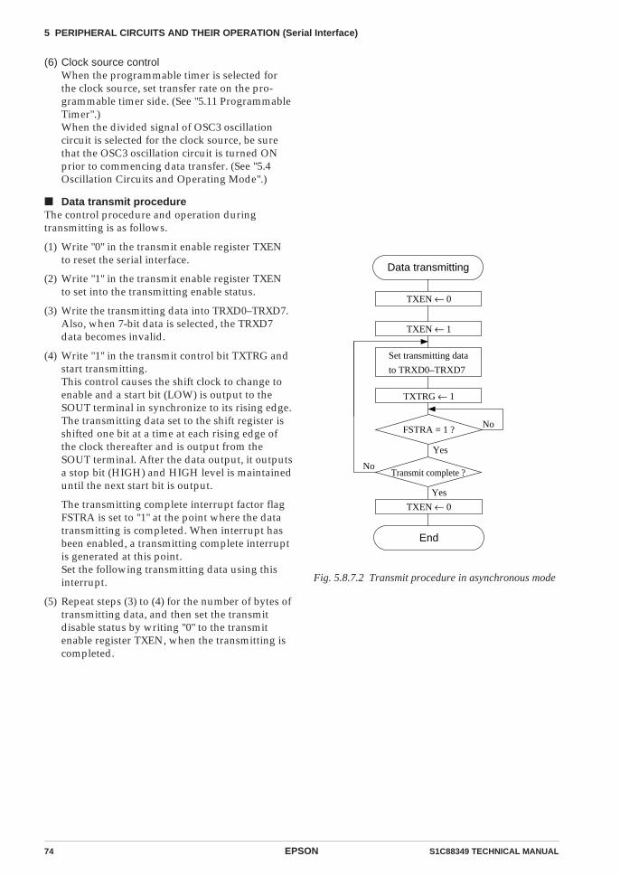
74 EPSON S1C88349 TECHNICAL MANUAL
5 PERIPHERAL CIRCUITS AND THEIR OPERATION (Serial Interface)
(6) Clock source controlWhen the programmable timer is selected forthe clock source, set transfer rate on the pro-grammable timer side. (See "5.11 ProgrammableTimer".)When the divided signal of OSC3 oscillationcircuit is selected for the clock source, be surethat the OSC3 oscillation circuit is turned ONprior to commencing data transfer. (See "5.4Oscillation Circuits and Operating Mode".)
Data transmit procedureThe control procedure and operation duringtransmitting is as follows.
(1) Write "0" in the transmit enable register TXENto reset the serial interface.
(2) Write "1" in the transmit enable register TXENto set into the transmitting enable status.
(3) Write the transmitting data into TRXD0–TRXD7.Also, when 7-bit data is selected, the TRXD7data becomes invalid.
(4) Write "1" in the transmit control bit TXTRG andstart transmitting.This control causes the shift clock to change toenable and a start bit (LOW) is output to theSOUT terminal in synchronize to its rising edge.The transmitting data set to the shift register isshifted one bit at a time at each rising edge ofthe clock thereafter and is output from theSOUT terminal. After the data output, it outputsa stop bit (HIGH) and HIGH level is maintaineduntil the next start bit is output.
The transmitting complete interrupt factor flagFSTRA is set to "1" at the point where the datatransmitting is completed. When interrupt hasbeen enabled, a transmitting complete interruptis generated at this point.Set the following transmitting data using thisinterrupt.
(5) Repeat steps (3) to (4) for the number of bytes oftransmitting data, and then set the transmitdisable status by writing "0" to the transmitenable register TXEN, when the transmitting iscompleted.
Data transmitting
End
TXEN ← 0
No
Yes
Transmit complete ?
Set transmitting data
to TRXD0–TRXD7
No
Yes
FSTRA = 1 ?
TXEN ← 0
TXTRG ← 1
TXEN ← 1
Fig. 5.8.7.2 Transmit procedure in asynchronous mode
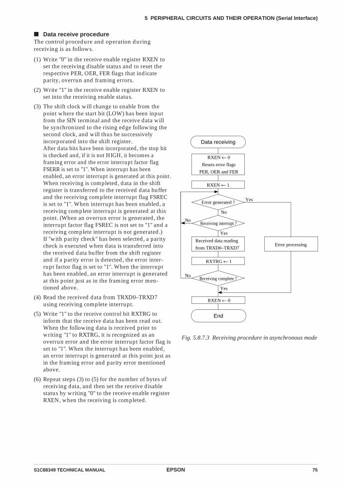
S1C88349 TECHNICAL MANUAL EPSON 75
5 PERIPHERAL CIRCUITS AND THEIR OPERATION (Serial Interface)
Data receive procedureThe control procedure and operation duringreceiving is as follows.
(1) Write "0" in the receive enable register RXEN toset the receiving disable status and to reset therespective PER, OER, FER flags that indicateparity, overrun and framing errors.
(2) Write "1" in the receive enable register RXEN toset into the receiving enable status.
(3) The shift clock will change to enable from thepoint where the start bit (LOW) has been inputfrom the SIN terminal and the receive data willbe synchronized to the rising edge following thesecond clock, and will thus be successivelyincorporated into the shift register.After data bits have been incorporated, the stop bitis checked and, if it is not HIGH, it becomes aframing error and the error interrupt factor flagFSERR is set to "1". When interrupt has beenenabled, an error interrupt is generated at this point.When receiving is completed, data in the shiftregister is transferred to the received data bufferand the receiving complete interrupt flag FSRECis set to "1". When interrupt has been enabled, areceiving complete interrupt is generated at thispoint. (When an overrun error is generated, theinterrupt factor flag FSREC is not set to "1" and areceiving complete interrupt is not generated.)If "with parity check" has been selected, a paritycheck is executed when data is transferred intothe received data buffer from the shift registerand if a parity error is detected, the error inter-rupt factor flag is set to "1". When the interrupthas been enabled, an error interrupt is generatedat this point just as in the framing error men-tioned above.
(4) Read the received data from TRXD0–TRXD7using receiving complete interrupt.
(5) Write "1" to the receive control bit RXTRG toinform that the receive data has been read out.When the following data is received prior towriting "1" to RXTRG, it is recognized as anoverrun error and the error interrupt factor flag isset to "1". When the interrupt has been enabled,an error interrupt is generated at this point just asin the framing error and parity error mentionedabove.
(6) Repeat steps (3) to (5) for the number of bytes ofreceiving data, and then set the receive disablestatus by writing "0" to the receive enable registerRXEN, when the receiving is completed.
End
RXEN ← 1
No
Yes
Receiving interrupt ?
Yes
Receiving complete ?
Received data reading
from TRXD0–TRXD7
RXEN ← 0
RXTRG ← 1
No
YesError generated ?
Error processing
Data receiving
RXEN ← 0
Resets error flags
PER, OER and FER
No
Fig. 5.8.7.3 Receiving procedure in asynchronous mode

76 EPSON S1C88349 TECHNICAL MANUAL
5 PERIPHERAL CIRCUITS AND THEIR OPERATION (Serial Interface)
Receive errorDuring receiving the following three types of errorscan be detected by an interrupt.
(1) Parity errorWhen writing "1" to the EPR register to select"with parity check", a parity check (verticalparity check) is executed during receiving. Aftereach data bit is sent a parity check bit is sent.The parity check bit is a "0" or a "1". Even paritychecking will cause the sum of the parity bitand the other bits to be even. Odd parity causesthe sum to be odd. This is checked on thereceiving side.The parity check is performed when datareceived in the shift register is transferred to thereceived data buffer. It checks whether theparity check bit is a "1" or a "0" (the sum of thebits including the parity bit) and the parity setin the PMD register match. When it does notmatch, it is recognized as an parity error and theparity error flag PER and the error interruptfactor flag FSERR are set to "1".When interrupt has been enabled, an errorinterrupt is generated at this point.The PER flag is reset to "0" by writing "1".Even when this error has been generated, thereceived data corresponding to the error istransferred in the received data buffer and thereceive operation also continues.The received data at this point cannot assuredbecause of the parity error.
(2) Framing errorIn asynchronous transfer, synchronization isadopted for each character at the start bit ("0")and the stop bit ("1"). When receiving has beendone with the stop bit set at "0", the serialinterface judges the synchronization to be offand a framing error is generated. When thiserror is generated, the framing error flag FERand the error interrupt factor flag FSERR are setto "1". When interrupt has been enabled, anerror interrupt is generated at this point.The FER flag is reset to "0" by writing "1".Even when this error has been generated, thereceived data for it is loaded into the receivedata buffer and the receive operation alsocontinues. However, even when it does notbecome a framing error with the following datareceipt, such data cannot be assured.Even when this error has been generated, thereceived data corresponding to the error istransferred in the received data buffer and thereceive operation also continues. However, evenwhen it does not become a framing error withthe following data receiving, such data cannotbe assured.
(3) Overrun errorWhen the next data is received before "1" iswritten to RXTRG, an overrun error will begenerated, because the previous receive datawill be overwritten. When this error is gener-ated, the overrun error flag OER and the errorinterrupt factor flag FSERR are set to "1". Wheninterrupt has been enabled, an error interrupt isgenerated at this point. The OER flag is reset to"0" by writing "1" into it.Even when this error has been generated, thereceived data corresponding to the error istransferred in the received data buffer and thereceive operation also continues.Furthermore, when the timing for writing "1" toRXTRG and the timing for the received datatransfer to the received data buffer overlap, itwill be recognized as an overrun error.
Timing chartFigure 5.8.7.4 show the asynchronous transfertiming chart.

S1C88349 TECHNICAL MANUAL EPSON 77
5 PERIPHERAL CIRCUITS AND THEIR OPERATION (Serial Interface)
TXEN
TXTRG(RD)
TXTRG(WR)
SOUT
Interrupt(In 8-bit mode/Non parity)
D0 D1 D2 D3 D4 D5 D6 D7
Samplingclock
(a) Transmit timing
RXEN
RXTRG(RD)
RXTRG(WR)
SIN
TRXD
OER control signal
OER
Interrupt
(In 8-bit mode/Non parity)D0 D1 D2 D3 D4 D5 D6 D7 D0 D1 D6 D7 D0 D1 D2 D3 D4 D5 D6 D7D2 D3 D4 D5
1st data 2nd data
Samplingclock
(b) Receive timing
Fig. 5.8.7.4 Timing chart (asynchronous transfer)
5.8.8 Interrupt functionThis serial interface includes a function thatgenerates the below indicated three types ofinterrupts.
• Transmitting complete interrupt• Receiving complete interrupt• Error interrupt
The interrupt factor flag FSxxx and the interruptenable register ESxxx for the respective interruptfactors are provided and then the interrupt enable/disable can be selected by the software. In addition,a priority level of the serial interface interrupt forthe CPU can be optionally set at levels 0 to 3 by theinterrupt priority registers PSIF0 and PSIF1.For details on the above mentioned interruptcontrol register and the operation followinggeneration of an interrupt, see "5.17 Interrupt andStandby Status".Figure 5.8.8.1 shows the configuration of the serialinterface interrupt circuit.
Transmitting complete interruptThis interrupt factor is generated at the point wherethe sending of the data written into the shiftregister has been completed and sets the interruptfactor flag FSTRA to "1". When set in this manner, ifthe corresponding interrupt enable register ESTRAis set to "1" and the corresponding interrupt priorityregisters PSIF0 and PSIF1 are set to a higher levelthan the setting of interrupt flags (I0 and I1), aninterrupt will be generated to the CPU.When "0" has been written into the interrupt enableregister ESTRA and interrupt has been disabled, aninterrupt is not generated to the CPU. Even in thiscase, the interrupt factor flag FSTRA is set to "1".The interrupt factor flag FSTRA is reset to "0" bywriting "1".The following transmitting data can be set and thetransmitting start (writing "1" to TXTRG) can becontrolled by generation of this interrupt factor.The exception processing vector address for thisinterrupt factor is set at 000014H.
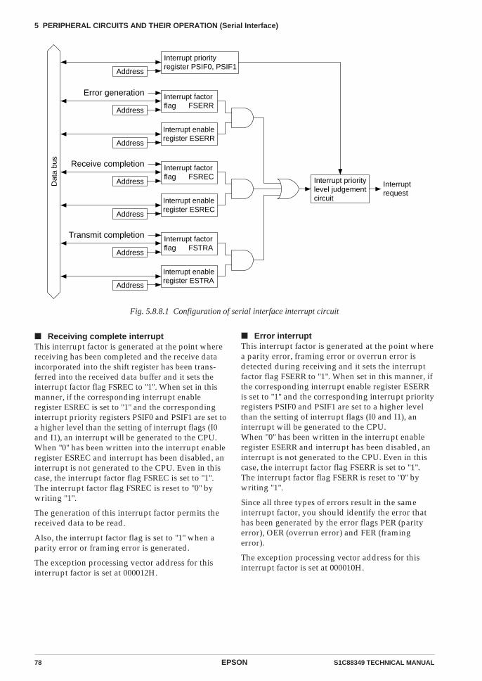
78 EPSON S1C88349 TECHNICAL MANUAL
5 PERIPHERAL CIRCUITS AND THEIR OPERATION (Serial Interface)
Dat
a bu
s
Interruptrequest
Address
Error generation Interrupt factorflag FSERR
Address
Interrupt enableregister ESERR
Address
Receive completion Interrupt factorflag FSREC
Address
Interrupt enableregister ESREC
Address
Transmit completion Interrupt factorflag FSTRA
Address
Interrupt enableregister ESTRA
Interrupt prioritylevel judgementcircuit
Address
Interrupt priority register PSIF0, PSIF1
Receiving complete interruptThis interrupt factor is generated at the point wherereceiving has been completed and the receive dataincorporated into the shift register has been trans-ferred into the received data buffer and it sets theinterrupt factor flag FSREC to "1". When set in thismanner, if the corresponding interrupt enableregister ESREC is set to "1" and the correspondinginterrupt priority registers PSIF0 and PSIF1 are set toa higher level than the setting of interrupt flags (I0and I1), an interrupt will be generated to the CPU.When "0" has been written into the interrupt enableregister ESREC and interrupt has been disabled, aninterrupt is not generated to the CPU. Even in thiscase, the interrupt factor flag FSREC is set to "1".The interrupt factor flag FSREC is reset to "0" bywriting "1".
The generation of this interrupt factor permits thereceived data to be read.
Also, the interrupt factor flag is set to "1" when aparity error or framing error is generated.
The exception processing vector address for thisinterrupt factor is set at 000012H.
Error interruptThis interrupt factor is generated at the point wherea parity error, framing error or overrun error isdetected during receiving and it sets the interruptfactor flag FSERR to "1". When set in this manner, ifthe corresponding interrupt enable register ESERRis set to "1" and the corresponding interrupt priorityregisters PSIF0 and PSIF1 are set to a higher levelthan the setting of interrupt flags (I0 and I1), aninterrupt will be generated to the CPU.When "0" has been written in the interrupt enableregister ESERR and interrupt has been disabled, aninterrupt is not generated to the CPU. Even in thiscase, the interrupt factor flag FSERR is set to "1".The interrupt factor flag FSERR is reset to "0" bywriting "1".
Since all three types of errors result in the sameinterrupt factor, you should identify the error thathas been generated by the error flags PER (parityerror), OER (overrun error) and FER (framingerror).
The exception processing vector address for thisinterrupt factor is set at 000010H.
Fig. 5.8.8.1 Configuration of serial interface interrupt circuit
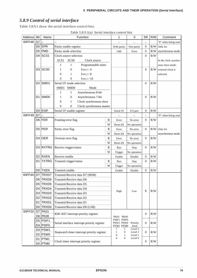
S1C88349 TECHNICAL MANUAL EPSON 79
5 PERIPHERAL CIRCUITS AND THEIR OPERATION (Serial Interface)
5.8.9 Control of serial interfaceTable 5.8.9.1 show the serial interface control bits.
Table 5.8.9.1(a) Serial interface control bitsAddress Bit Name
00FF48 D7
D6
D5
D4
D3
D2
D1
D0
–
EPR
PMD
SCS1
SCS0
SMD1
SMD0
ESIF
SR R/WFunction Comment
–
Parity enable register
Parity mode selection
Clock source selection
Serial I/F mode selection
Serial I/F enable register
"0" when being read
Only for
asynchronous mode
In the clock synchro-
nous slave mode,
external clock is
selected.
1 0
–
0
0
0
0
0
0
0
R/W
R/W
R/W
R/W
R/W
R/W
R/W
–
With parity
Odd
Serial I/F
–
Non parity
Even
I/O port
SCS1
1
1
0
0
SCS0
1
0
1
0
Clock source
Programmable timer
fOSC3 / 4
fOSC3 / 8
fOSC3 / 16
SMD1
1
1
0
0
SMD0
1
0
1
0
Mode
Asynchronous 8-bit
Asynchronous 7-bit
Clock synchronous slave
Clock synchronous master
00FF49 D7
D6
D5
D4
D3
D2
D1
D0
–
FER
PER
OER
RXTRG
RXEN
TXTRG
TXEN
–
Framing error flag
Parity error flag
Overrun error flag
Receive trigger/status
Receive enable
Transmit trigger/status
Transmit enable
"0" when being read
Only for
asynchronous mode
–
0
0
0
0
0
0
0
R/W
R/W
R/W
R/W
R/W
R/W
R/W
–
Error
Reset (0)
Error
Reset (0)
Error
Reset (0)
Run
Trigger
Enable
Run
Trigger
Enable
–
No error
No operation
No error
No operation
No error
No operation
Stop
No operation
Disable
Stop
No operation
Disable
00FF4A D7
D6
D5
D4
D3
D2
D1
D0
TRXD7
TRXD6
TRXD5
TRXD4
TRXD3
TRXD2
TRXD1
TRXD0
X R/WHigh Low
Transmit/Receive data D7 (MSB)
Transmit/Receive data D6
Transmit/Receive data D5
Transmit/Receive data D4
Transmit/Receive data D3
Transmit/Receive data D2
Transmit/Receive data D1
Transmit/Receive data D0 (LSB)
R
W
R
W
R
W
R
W
R
W
00FF20 D7
D6
D5
D4
D3
D2
D1
D0
PK01
PK00
PSIF1
PSIF0
PSW1
PSW0
PTM1
PTM0
K00–K07 interrupt priority register
Serial interface interrupt priority register
Stopwatch timer interrupt priority register
Clock timer interrupt priority register
0
0
0
0
R/W
R/W
R/W
R/W
PK01PSIF1PSW1PTM1
1100
PK00PSIF0PSW0PTM0
1010
Prioritylevel
Level 3Level 2Level 1Level 0
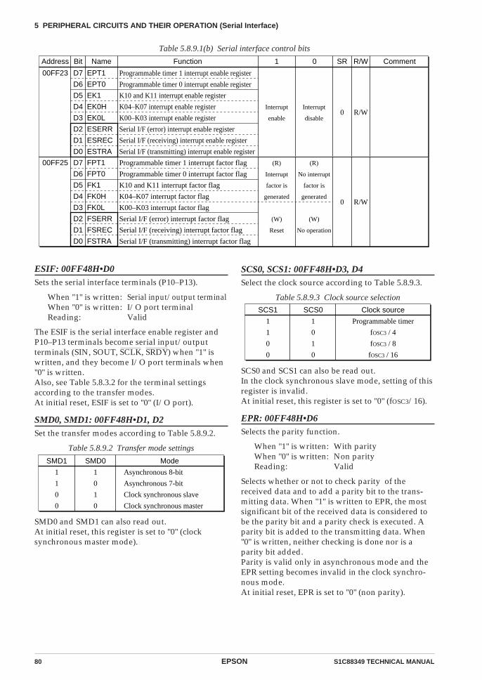
80 EPSON S1C88349 TECHNICAL MANUAL
5 PERIPHERAL CIRCUITS AND THEIR OPERATION (Serial Interface)
SCS0, SCS1: 00FF48H•D3, D4Select the clock source according to Table 5.8.9.3.
Table 5.8.9.3 Clock source selection
ESIF: 00FF48H•D0Sets the serial interface terminals (P10–P13).
When "1" is written: Serial input/output terminalWhen "0" is written: I/O port terminalReading: Valid
The ESIF is the serial interface enable register andP10–P13 terminals become serial input/outputterminals (SIN, SOUT, SCLK, SRDY) when "1" iswritten, and they become I/O port terminals when"0" is written.Also, see Table 5.8.3.2 for the terminal settingsaccording to the transfer modes.At initial reset, ESIF is set to "0" (I/O port).
SMD0, SMD1: 00FF48H•D1, D2Set the transfer modes according to Table 5.8.9.2.
Table 5.8.9.2 Transfer mode settings
SMD1 SMD0 Mode
1
1
0
0
1
0
1
0
Asynchronous 8-bit
Asynchronous 7-bit
Clock synchronous slave
Clock synchronous master
SMD0 and SMD1 can also read out.At initial reset, this register is set to "0" (clocksynchronous master mode).
SCS1
1
1
0
0
SCS0
1
0
1
0
Clock source
Programmable timer
fOSC3 / 4
fOSC3 / 8
fOSC3 / 16
SCS0 and SCS1 can also be read out.In the clock synchronous slave mode, setting of thisregister is invalid.At initial reset, this register is set to "0" (fOSC3/16).
EPR: 00FF48H•D6Selects the parity function.
When "1" is written: With parityWhen "0" is written: Non parityReading: Valid
Selects whether or not to check parity of thereceived data and to add a parity bit to the trans-mitting data. When "1" is written to EPR, the mostsignificant bit of the received data is considered tobe the parity bit and a parity check is executed. Aparity bit is added to the transmitting data. When"0" is written, neither checking is done nor is aparity bit added.Parity is valid only in asynchronous mode and theEPR setting becomes invalid in the clock synchro-nous mode.At initial reset, EPR is set to "0" (non parity).
Table 5.8.9.1(b) Serial interface control bits
Address Bit Name SR R/WFunction Comment1 0
D7
D6
D5
D4
D3
D2
D1
D0
00FF25 D7
D6
D5
D4
D3
D2
D1
D0
FPT1
FPT0
FK1
FK0H
FK0L
FSERR
FSREC
FSTRA
Programmable timer 1 interrupt factor flag
Programmable timer 0 interrupt factor flag
K10 and K11 interrupt factor flag
K04–K07 interrupt factor flag
K00–K03 interrupt factor flag
Serial I/F (error) interrupt factor flag
Serial I/F (receiving) interrupt factor flag
Serial I/F (transmitting) interrupt factor flag
0 R/W
(R)
Interrupt
factor is
generated
(W)
Reset
(R)
No interrupt
factor is
generated
(W)
No operation
00FF23 EPT1
EPT0
EK1
EK0H
EK0L
ESERR
ESREC
ESTRA
Programmable timer 1 interrupt enable register
Programmable timer 0 interrupt enable register
K10 and K11 interrupt enable register
K04–K07 interrupt enable register
K00–K03 interrupt enable register
Serial I/F (error) interrupt enable register
Serial I/F (receiving) interrupt enable register
Serial I/F (transmitting) interrupt enable register
0 R/WInterrupt
enable
Interrupt
disable
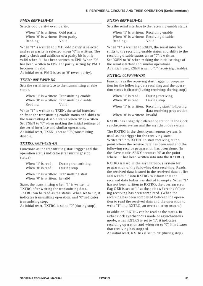
S1C88349 TECHNICAL MANUAL EPSON 81
5 PERIPHERAL CIRCUITS AND THEIR OPERATION (Serial Interface)
PMD: 00FF48H•D5Selects odd parity/even parity.
When "1" is written: Odd parityWhen "0" is written: Even parityReading: Valid
When "1" is written to PMD, odd parity is selectedand even parity is selected when "0" is written. Theparity check and addition of a parity bit is onlyvalid when "1" has been written to EPR. When "0"has been written to EPR, the parity setting by PMDbecomes invalid.At initial reset, PMD is set to "0" (even parity).
TXEN: 00FF49H•D0Sets the serial interface to the transmitting enablestatus.
When "1" is written: Transmitting enableWhen "0" is written: Transmitting disableReading: Valid
When "1" is written to TXEN, the serial interfaceshifts to the transmitting enable status and shifts tothe transmitting disable status when "0" is written.Set TXEN to "0" when making the initial settings ofthe serial interface and similar operations.At initial reset, TXEN is set to "0" (transmittingdisable).
TXTRG: 00FF49H•D1Functions as the transmitting start trigger and theoperation status indicator (transmitting/stopstatus).
When "1" is read: During transmittingWhen "0" is read: During stop
When "1" is written: Transmitting startWhen "0" is written: Invalid
Starts the transmitting when "1" is written toTXTRG after writing the transmitting data.TXTRG can be read as the status. When set to "1", itindicates transmitting operation, and "0" indicatestransmitting stop.At initial reset, TXTRG is set to "0" (during stop).
RXEN: 00FF49H•D2Sets the serial interface to the receiving enable status.
When "1" is written: Receiving enableWhen "0" is written: Receiving disableReading: Valid
When "1" is written to RXEN, the serial interfaceshifts to the receiving enable status and shifts to thereceiving disable status when "0" is written.Set RXEN to "0" when making the initial settings ofthe serial interface and similar operations.At initial reset, RXEN is set to "0" (receiving disable).
RXTRG: 00FF49H•D3Functions as the receiving start trigger or prepara-tion for the following data receiving and the opera-tion status indicator (during receiving/during stop).
When "1" is read: During receivingWhen "0" is read: During stop
When "1" is written: Receiving start/followingdata receiving preparation
When "0" is written: Invalid
RXTRG has a slightly different operation in the clocksynchronous system and the asynchronous system.
The RXTRG in the clock synchronous system, isused as the trigger for the receiving start.Writes "1" into RXTRG to start receiving at thepoint where the receive data has been read and thefollowing receive preparation has been done. (Inthe slave mode, SRDY becomes "0" at the pointwhere "1" has been written into into the RXTRG.)
RXTRG is used in the asynchronous system forpreparation of the following data receiving. Readsthe received data located in the received data bufferand writes "1" into RXTRG to inform that thereceived data buffer has shifted to empty. When "1"has not been written to RXTRG, the overrun errorflag OER is set to "1" at the point where the follow-ing receiving has been completed. (When thereceiving has been completed between the opera-tion to read the received data and the operation towrite "1" into RXTRG, an overrun error occurs.)
In addition, RXTRG can be read as the status. Ineither clock synchronous mode or asynchronousmode, when RXTRG is set to "1", it indicatesreceiving operation and when set to "0", it indicatesthat receiving has stopped.At initial reset, RXTRG is set to "0" (during stop).
82 EPSON S1C88349 TECHNICAL MANUAL
5 PERIPHERAL CIRCUITS AND THEIR OPERATION (Serial Interface)
TRXD0–TRXD7: 00FF4AHDuring transmittingWrite the transmitting data into the transmit shiftregister.
When "1" is written: HIGH levelWhen "0" is written: LOW level
Write the transmitting data prior to startingtransmitting.In the case of continuous transmitting, wait for thetransmitting complete interrupt, then write the data.The TRXD7 becomes invalid for the asynchronous7-bit mode.Converted serial data for which the bits set at "1" asHIGH (VDD) level and for which the bits set at "0"as LOW (VSS) level are output from the SOUTterminal.
During receivingRead the received data.
When "1" is read: HIGH levelWhen "0" is read: LOW level
The data from the received data buffer can be read out.Since the sift register is provided separately fromthis buffer, reading can be done during the receiveoperation in the asynchronous mode. (The bufferfunction is not used in the clock synchronous mode.)Read the data after waiting for the receivingcomplete interrupt.When performing parity check in the asynchronous7-bit mode, "0" is loaded into the 8th bit (TRXD7)that corresponds to the parity bit.The serial data input from the SIN terminal is levelconverted, making the HIGH (VDD) level bit "1" andthe LOW (VSS) level bit "0" and is then loaded intothis buffer.At initial reset, the buffer content is undefined.
OER: 00FF49H•D4Indicates the generation of an overrun error.
When "1" is read: ErrorWhen "0" is read: No error
When "1" is written: Reset to "0"When "0" is written: Invalid
OER is an error flag that indicates the generation ofan overrun error and becomes "1" when an errorhas been generated.An overrun error is generated when the receivingof data has been completed prior to the writing of"1" to RXTRG in the asynchronous mode.OER is reset to "0" by writing "1".At initial reset and when RXEN is "0", OER is set to"0" (no error).
PER: 00FF49H•D5Indicates the generation of a parity error.
When "1" is read: ErrorWhen "0" is read: No error
When "1" is written: Reset to "0"When "0" is written: Invalid
PER is an error flag that indicates the generation ofa parity error and becomes "1" when an error hasbeen generated.When a parity check is performed in the asynchro-nous mode, if data that does not match the parity isreceived, a parity error is generated.PER is reset to "0" by writing "1".At initial reset and when RXEN is "0", PER is set to"0" (no error).
FER: 00FF49H•D6Indicates the generation of a framing error.
When "1" is read: ErrorWhen "0" is read: No error
When "1" is written: Reset to "0"When "0" is written: Invalid
FER is an error flag that indicates the generation ofa framing error and becomes "1" when an error hasbeen generated.When the stop bit for the receiving of the asynchro-nous mode has become "0", a framing error isgenerated.FER is reset to "0" by writing "1".At initial reset and when RXEN is "0", FER is set to"0" (no error).
PSIF0, PSIF1: 00FF20H•D4, D5Sets the priority level of the serial interface interrupt.The two bits PSIF0 and PSIF1 are the interruptpriority register corresponding to the serial inter-face interrupt. Table 5.8.9.4 shows the interruptpriority level which can be set by this register.
Table 5.8.9.4 Interrupt priority level settings
PSIF1 PSIF0 Interrupt priority level
1
1
0
0
1
0
1
0
Level 3 (IRQ3)
Level 2 (IRQ2)
Level 1 (IRQ1)
Level 0 (None)
At initial reset, this register is set to "0" (level 0).
S1C88349 TECHNICAL MANUAL EPSON 83
5 PERIPHERAL CIRCUITS AND THEIR OPERATION (Serial Interface)
ESTRA, ESREC, ESERR: 00FF23H•D0, D1, D2Enables or disables the generation of an interruptfor the CPU.
When "1" is written: Interrupt enabledWhen "0" is written: Interrupt disabledReading: Valid
ESTRA, ESREC and ESERR are interrupt enableregisters that respectively correspond to the inter-rupt factors for transmitting complete, receivingcomplete and receiving error. Interrupts set to "1"are enabled and interrupts set to "0" are disabled.At initial reset, this register is set to "0" (interruptdisabled).
FSTRA, FSREC, FSERR: 00FF25H•D0, D1, D2Indicates the serial interface interrupt generation status.
When "1" is read: Interrupt factor presentWhen "0" is read: Interrupt factor not present
When "1" is written: Resets factor flagWhen "0" is written: Invalid
FSTRA, FSREC and FSERR are interrupt factor flagsthat respectively correspond to the interrupts fortransmitting complete, receiving complete andreceiving error and are set to "1" by generation ofeach factor.Transmitting complete interrupt factor is generatedat the point where the data transmitting of the shiftregister has been completed.Receiving complete interrupt factor is generated atthe point where the received data has been trans-ferred into the received data buffer.Receive error interrupt factor is generated when aparity error, framing error or overrun error has beendetected during data receiving.When set in this manner, if the correspondinginterrupt enable register is set to "1" and the corre-sponding interrupt priority register is set to a higherlevel than the setting of interrupt flags (I0 and I1), aninterrupt will be generated to the CPU.Regardless of the interrupt enable register andinterrupt priority register settings, the interruptfactor flag will be set to "1" by the occurrence of aninterrupt generation condition.To accept the subsequent interrupt after interruptgeneration, re-setting of the interrupt flags (setinterrupt flag to lower level than the level indicatedby the interrupt priority registers, or execute theRETE instruction) and interrupt factor flag reset arenecessary. The interrupt factor flag is reset to "0" bywriting "1".At initial reset, this flag is reset to "0".
5.8.10 Programming notes(1) Be sure to initialize the serial interface mode in
the transmitting/receiving disable status (TXEN= RXEN = "0").
(2) Do not perform double trigger (writing "1") toTXTRG (RXTRG) when the serial interface is in thetransmitting (receiving) operation. Furthermore, donot execute the SLP instruction. (When executingthe SLP instruction, set TXEN = RXEN = "0".)
(3) In the clock synchronous mode, since one clockline (SCLK) is shared for both transmitting andreceiving, transmitting and receiving cannot beperformed simultaneously. (Half duplex only ispossible in clock synchronous mode.)Consequently, be sure not to write "1" toRXTRG (TXTRG) when TXTRG (RXTRG) is "1".
(4) When a parity error or flaming error is generatedduring receiving in the asynchronous mode, thereceiving error interrupt factor flag FSERR is setto "1" prior to the receiving complete interruptfactor flag FSREC for the time indicated in Table5.8.10.1. Consequently, when an error is generated,you should reset the receiving complete interruptfactor flag FSREC to "0" by providing a wait time inerror processing routines and similar routines.When an overrun error is generated, the receivingcomplete interrupt factor flag FSREC is not set to "1"and a receiving complete interrupt is not generated.
Table 5.8.10.1 Time difference between FSERR and FSREC on error generation
Clock source Time difference
fOSC3 / n
Programmable timer
1/2 cycles of fOSC3 / n
1 cycle of timer 1 underflow
(5) When the demultiplied signal of the OSC3oscillation circuit is made the clock source, it isnecessary to turn the OSC3 oscillation ON, prior tousing the serial interface.A time interval of several msec to several 10 msec,from the turning ON of the OSC3 oscillationcircuit to until the oscillation stabilizes, is neces-sary, due to the oscillation element that is used.Consequently, you should allow an adequatewaiting time after turning ON of the OSC3oscillation, before starting transmitting/receivingof serial interface. (The oscillation start time willvary somewhat depending on the oscillator and onthe externally attached parts. Refer to theoscillation start time example indicated in Chapter8, "ELECTRICAL CHARACTERISTICS".)At initial reset, the OSC3 oscillation circuit is set toOFF status.
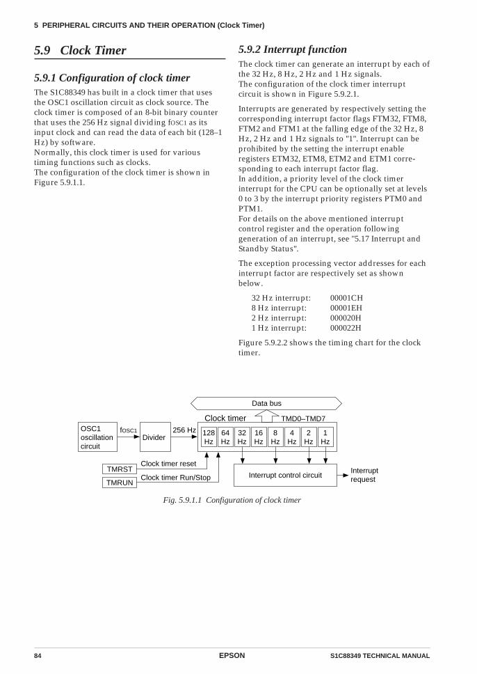
84 EPSON S1C88349 TECHNICAL MANUAL
5 PERIPHERAL CIRCUITS AND THEIR OPERATION (Clock Timer)
5.9 Clock Timer
5.9.1 Configuration of clock timerThe S1C88349 has built in a clock timer that usesthe OSC1 oscillation circuit as clock source. Theclock timer is composed of an 8-bit binary counterthat uses the 256 Hz signal dividing fOSC1 as itsinput clock and can read the data of each bit (128–1Hz) by software.Normally, this clock timer is used for varioustiming functions such as clocks.The configuration of the clock timer is shown inFigure 5.9.1.1.
5.9.2 Interrupt functionThe clock timer can generate an interrupt by each ofthe 32 Hz, 8 Hz, 2 Hz and 1 Hz signals.The configuration of the clock timer interruptcircuit is shown in Figure 5.9.2.1.
Interrupts are generated by respectively setting thecorresponding interrupt factor flags FTM32, FTM8,FTM2 and FTM1 at the falling edge of the 32 Hz, 8Hz, 2 Hz and 1 Hz signals to "1". Interrupt can beprohibited by the setting the interrupt enableregisters ETM32, ETM8, ETM2 and ETM1 corre-sponding to each interrupt factor flag.In addition, a priority level of the clock timerinterrupt for the CPU can be optionally set at levels0 to 3 by the interrupt priority registers PTM0 andPTM1.For details on the above mentioned interruptcontrol register and the operation followinggeneration of an interrupt, see "5.17 Interrupt andStandby Status".
The exception processing vector addresses for eachinterrupt factor are respectively set as shownbelow.
32 Hz interrupt: 00001CH8 Hz interrupt: 00001EH2 Hz interrupt: 000020H1 Hz interrupt: 000022H
Figure 5.9.2.2 shows the timing chart for the clocktimer.
Data bus
InterruptrequestInterrupt control circuit
OSC1oscillationcircuit
64Hz
32Hz
16Hz
8Hz
4Hz
2Hz
1Hz
128Hz
Clock timer resetTMRST
Clock timer TMD0–TMD7
TMRUNClock timer Run/Stop
DividerfOSC1 256 Hz
Fig. 5.9.1.1 Configuration of clock timer

S1C88349 TECHNICAL MANUAL EPSON 85
5 PERIPHERAL CIRCUITS AND THEIR OPERATION (Clock Timer)
256 Hz
128 Hz
64 Hz
32 Hz
16 Hz
8 Hz
4 Hz
2 Hz
1 Hz
32 Hz interrupt
8 Hz interrupt
2 Hz interrupt
1 Hz interrupt
OSC1/128
TMD0
TMD1
TMD2
TMD3
TMD4
TMD5
TMD6
TMD7
Dat
a bu
s
Interruptrequest
Address
32 Hz falling edge Interrupt factorflag FTM32
Address
Interrupt enableregister ETM32
Address
8 Hz falling edge Interrupt factorflag FTM8
Address
Interrupt enableregister ETM8
Address
2 Hz falling edge Interrupt factorflag FTM2
Address
Interrupt enableregister ETM2
Interrupt prioritylevel judgementcircuit
Address
Interrupt priority register PTM0, PTM1
Address
1 Hz falling edge Interrupt factorflag FTM1
Address
Interrupt enableregister ETM1
Fig. 5.9.2.1 Configuration of clock timer interrupt circuit
Fig. 5.9.2.2 Timing chart of clock timer
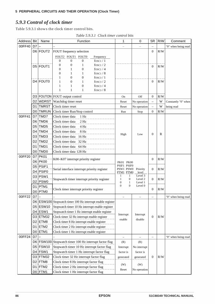
86 EPSON S1C88349 TECHNICAL MANUAL
5 PERIPHERAL CIRCUITS AND THEIR OPERATION (Clock Timer)
5.9.3 Control of clock timerTable 5.9.3.1 shows the clock timer control bits.
Table 5.9.3.1 Clock timer control bits
Address Bit Name
00FF40 D7
D6
D5
D4
D3
D2
D1
D0
–
FOUT2
FOUT1
FOUT0
FOUTON
WDRST
TMRST
TMRUN
SR R/WFunction Comment
–
FOUT frequency selection
FOUT output control
Watchdog timer reset
Clock timer reset
Clock timer Run/Stop control
"0" when being read
Constantly "0" when
being read
1 0
–
0
0
0
0
–
–
0
R/W
R/W
R/W
R/W
W
W
R/W
–
On
Reset
Reset
Run
–
Off
No operation
No operation
Stop
00FF41 D7
D6
D5
D4
D3
D2
D1
D0
TMD7
TMD6
TMD5
TMD4
TMD3
TMD2
TMD1
TMD0
Clock timer data
Clock timer data
Clock timer data
Clock timer data
Clock timer data
Clock timer data
Clock timer data
Clock timer data
0 RHigh Low
1 Hz
2 Hz
4 Hz
8 Hz
16 Hz
32 Hz
64 Hz
128 Hz
FOUT2
00001111
FOUT1
00110011
FOUT0
01010101
Frequency
fOSC1 / 1fOSC1 / 2fOSC1 / 4fOSC1 / 8fOSC3 / 1fOSC3 / 2fOSC3 / 4fOSC3 / 8
00FF20 D7
D6
D5
D4
D3
D2
D1
D0
PK01
PK00
PSIF1
PSIF0
PSW1
PSW0
PTM1
PTM0
K00–K07 interrupt priority register
Serial interface interrupt priority register
Stopwatch timer interrupt priority register
Clock timer interrupt priority register
0
0
0
0
R/W
R/W
R/W
R/W
PK01PSIF1PSW1PTM1
1100
PK00PSIF0PSW0PTM0
1010
Prioritylevel
Level 3Level 2Level 1Level 0
00FF22 D7
D6
D5
D4
D3
D2
D1
D0
–
ESW100
ESW10
ESW1
ETM32
ETM8
ETM2
ETM1
–
Stopwatch timer 100 Hz interrupt enable register
Stopwatch timer 10 Hz interrupt enable register
Stopwatch timer 1 Hz interrupt enable register
Clock timer 32 Hz interrupt enable register
Clock timer 8 Hz interrupt enable register
Clock timer 2 Hz interrupt enable register
Clock timer 1 Hz interrupt enable register
"0" when being read–
0 R/W
–
Interrupt
enable
–
Interrupt
disable
00FF24 D7
D6
D5
D4
D3
D2
D1
D0
–
FSW100
FSW10
FSW1
FTM32
FTM8
FTM2
FTM1
–
Stopwatch timer 100 Hz interrupt factor flag
Stopwatch timer 10 Hz interrupt factor flag
Stopwatch timer 1 Hz interrupt factor flag
Clock timer 32 Hz interrupt factor flag
Clock timer 8 Hz interrupt factor flag
Clock timer 2 Hz interrupt factor flag
Clock timer 1 Hz interrupt factor flag
"0" when being read–
0 R/W
–
(R)
Interrupt
factor is
generated
(W)
Reset
–
(R)
No interrupt
factor is
generated
(W)
No operation
S1C88349 TECHNICAL MANUAL EPSON 87
5 PERIPHERAL CIRCUITS AND THEIR OPERATION (Clock Timer)
TMD0–TMD7: 00FF41HThe clock timer data can be read out.Each bit of TMD0–TMD7 and frequency corre-spondence are as follows:
TMD0: 128 Hz TMD4: 8 HzTMD1: 64 Hz TMD5: 4 HzTMD2: 32 Hz TMD6: 2 HzTMD3: 16 Hz TMD7: 1 Hz
Since the TMD0–TMD7 is exclusively for reading,the write operation is invalid.At initial reset, the timer data is set to "00H".
TMRST: 00FF40H•D1Resets the clock timer.
When "1" is written: Clock timer resetWhen "0" is written: No operationReading: Always "0"
The clock timer is reset by writing "1" to theTMRST.When the clock timer is reset in the RUN status, itrestarts immediately after resetting. In the case ofthe STOP status, the reset data "00H" is maintained.No operation results when "0" is written to theTMRST.Since the TMRST is exclusively for writing, italways becomes "0" during reading.
TMRUN: 00FF40H•D0Controls RUN/STOP of the clock timer.
When "1" is written: RUNWhen "0" is written: STOPReading: Valid
The clock timer starts up-counting by writing "1" tothe TMRUN and stops by writing "0".In the STOP status, the count data is maintaineduntil it is reset or set in the next RUN status. Also,when the STOP status changes to the RUN status,the data that was maintained can be used forresuming the count.At initial reset, the TMRUN is set to "0" (STOP).
PTM0, PTM1: 00FF20H•D0, D1Sets the priority level of the clock timer interrupt.The two bits PTM0 and PTM1 are the interruptpriority register corresponding to the clock timerinterrupt. Table 5.9.3.2 shows the interrupt prioritylevel which can be set by this register.
Table 5.9.3.2 Interrupt priority level settings
At initial reset, this register is set to "0" (level 0).
PTM1 PTM0 Interrupt priority level
1
1
0
0
1
0
1
0
Level 3 (IRQ3)
Level 2 (IRQ2)
Level 1 (IRQ1)
Level 0 (None)
ETM1, ETM2, ETM8, ETM32: 00FF22H•D0–D3Enables or disables the generation of an interruptfor the CPU.
When "1" is written: Interrupt enabledWhen "0" is written: Interrupt disabledReading: Valid
The ETM1, ETM2, ETM8 and ETM32 are interruptenable registers that respectively correspond to theinterrupt factors for 1 Hz, 2 Hz, 8 Hz and 32 Hz.Interrupts set to "1" are enabled and interrupts setto "0" are disabled.At initial reset, this register is set to "0" (interruptdisabled).
FTM1, FTM2, FTM8, FTM32: 00FF24H•D0–D3Indicates the clock timer interrupt generation status.
When "1" is read: Interrupt factor presentWhen "0" is read: Interrupt factor not present
When "1" is written: Resets factor flagWhen "0" is written: Invalid
The FTM1, FTM2, FTM8 and FTM32 are interruptfactor flags that respectively correspond to theinterrupts for 1 Hz, 2 Hz, 8 Hz and 32 Hz and areset to "1" at the falling edge of each signal.When set in this manner, if the correspondinginterrupt enable register is set to "1" and thecorresponding interrupt priority register is set to ahigher level than the setting of interrupt flags (I0and I1), an interrupt will be generated to the CPU.Regardless of the interrupt enable register andinterrupt priority register settings, the interruptfactor flag will be set to "1" by the occurrence of aninterrupt generation condition.To accept the subsequent interrupt after interruptgeneration, re-setting of the interrupt flags (setinterrupt flag to lower level than the level indicatedby the interrupt priority registers, or execute theRETE instruction) and interrupt factor flag reset arenecessary. The interrupt factor flag is reset to "0" bywriting "1".At initial reset, this flag is reset to "0".
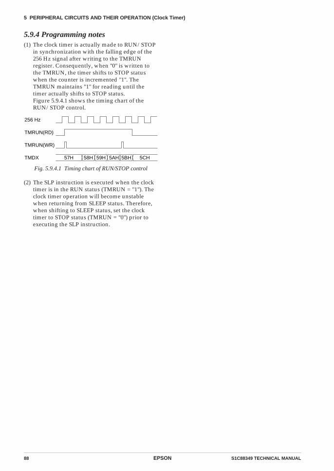
88 EPSON S1C88349 TECHNICAL MANUAL
5 PERIPHERAL CIRCUITS AND THEIR OPERATION (Clock Timer)
5.9.4 Programming notes(1) The clock timer is actually made to RUN/STOP
in synchronization with the falling edge of the256 Hz signal after writing to the TMRUNregister. Consequently, when "0" is written tothe TMRUN, the timer shifts to STOP statuswhen the counter is incremented "1". TheTMRUN maintains "1" for reading until thetimer actually shifts to STOP status.Figure 5.9.4.1 shows the timing chart of theRUN/STOP control.
Fig. 5.9.4.1 Timing chart of RUN/STOP control
(2) The SLP instruction is executed when the clocktimer is in the RUN status (TMRUN = "1"). Theclock timer operation will become unstablewhen returning from SLEEP status. Therefore,when shifting to SLEEP status, set the clocktimer to STOP status (TMRUN = "0") prior toexecuting the SLP instruction.
TMRUN(WR)
TMDX 57H 58H 59H 5AH 5BH 5CH
TMRUN(RD)
256 Hz
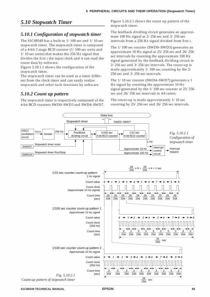
S1C88349 TECHNICAL MANUAL EPSON 89
5 PERIPHERAL CIRCUITS AND THEIR OPERATION (Stopwatch Timer)
5.10 Stopwatch Timer
5.10.1 Configuration of stopwatch timerThe S1C88349 has a built-in 1/100 sec and 1/10 secstopwatch timer. The stopwatch timer is composedof a 4-bit 2 stage BCD counter (1/100 sec units and1/10 sec units) that makes the 256 Hz signal thatdivides the fOSC1 the input clock and it can read thecount data by software.Figure 5.10.1.1 shows the configuration of thestopwatch timer.The stopwatch timer can be used as a timer differ-ent from the clock timer and can easily realizestopwatch and other such functions by software.
Figure 5.10.2.1 shows the count up pattern of thestopwatch timer.
The feedback dividing circuit generates an approxi-mate 100 Hz signal at 2/256 sec and 3/256 secintervals from a 256 Hz signal divided from fOSC1.
The 1/100 sec counter (SWD0–SWD3) generates anapproximate 10 Hz signal at 25/256 sec and 26/256sec intervals by counting the approximate 100 Hzsignal generated by the feedback dividing circuit in2/256 sec and 3/256 sec intervals. The count-up ismade approximately 1/100 sec counting by the 2/256 sec and 3/256 sec intervals.
The 1/10 sec counter (SWD4–SWD7) generates a 1Hz signal by counting the approximate 10 Hzsignal generated by the 1/100 sec counter at 25/256sec and 26/256 sec intervals in 4:6 ratios.
The count-up is made approximately 1/10 seccounting by 25/256 sec and 26/256 sec intervals.
5.10.2 Count up patternThe stopwatch timer is respectively composed of the4-bit BCD counters SWD0–SWD3 and SWD4–SWD7.
Data bus
Interruptrequest
Divider256 Hz
Stopwatch timer reset
SWRUN
Stopwatch timer SWD0–SWD7
1 Hz
SWRST
OSC1oscillationcircuit
fOSC1
Stopwatch timer Run/Stop Approximate 100 Hz
Approximate 10 Hz
Feedbackdividing circuit
Interruptcontrolcircuit
1/100 sec4-bit BCD counter
1/10 sec4-bit BCD counter
Fig. 5.10.1.1Configuration ofstopwatch timer
1/10 sec counter count-up pattern
26256
0
26256
1
25256
2
25256
3
26256
4
26256
5
25256
6
25256
7
26256
8
26256
9 0Count value
Count clock(Approximate 10 Hz signal)
Count time(sec)
3256
0
2256
1
3256
2
2256
3
3256
4
2256
5
3256
6
2256
7
3256
8
2256
9 0Count value
Count clock(256 Hz)
Count time(sec)
3256
0
3256
1
3256
2
2256
3
3256
4
2256
5
3256
6
2256
7
3256
8
2256
9 0Count value
Count clock(256 Hz)
Count time(sec)
25256
26256
sec
sec
1/100 sec counter count-up pattern 1Approximate 10 Hz signal
1/100 sec counter count-up pattern 2Approximate 10 Hz signal
1 Hz signal
26256
x 6 + 25256
x 4 = 1 sec
Fig. 5.10.2.1Count-up pattern of stopwatch timer
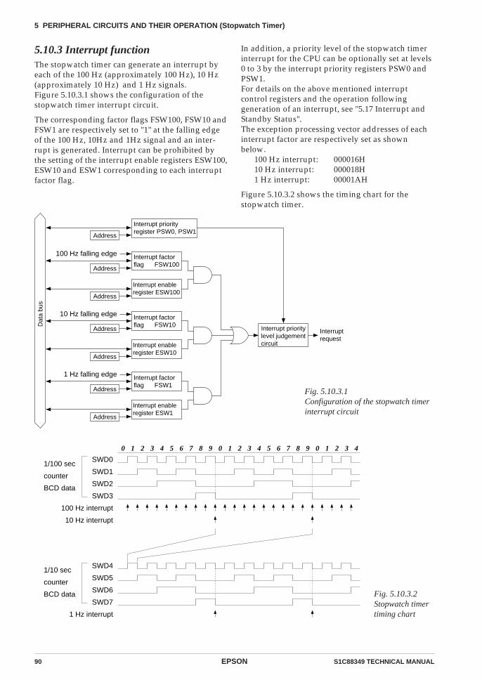
90 EPSON S1C88349 TECHNICAL MANUAL
5 PERIPHERAL CIRCUITS AND THEIR OPERATION (Stopwatch Timer)
5.10.3 Interrupt functionThe stopwatch timer can generate an interrupt byeach of the 100 Hz (approximately 100 Hz), 10 Hz(approximately 10 Hz) and 1 Hz signals.Figure 5.10.3.1 shows the configuration of thestopwatch timer interrupt circuit.
The corresponding factor flags FSW100, FSW10 andFSW1 are respectively set to "1" at the falling edgeof the 100 Hz, 10Hz and 1Hz signal and an inter-rupt is generated. Interrupt can be prohibited bythe setting of the interrupt enable registers ESW100,ESW10 and ESW1 corresponding to each interruptfactor flag.
In addition, a priority level of the stopwatch timerinterrupt for the CPU can be optionally set at levels0 to 3 by the interrupt priority registers PSW0 andPSW1.For details on the above mentioned interruptcontrol registers and the operation followinggeneration of an interrupt, see "5.17 Interrupt andStandby Status".The exception processing vector addresses of eachinterrupt factor are respectively set as shownbelow.
100 Hz interrupt: 000016H10 Hz interrupt: 000018H1 Hz interrupt: 00001AH
Figure 5.10.3.2 shows the timing chart for thestopwatch timer.
SWD0
SWD1
SWD2
SWD3
100 Hz interrupt
10 Hz interrupt
1/100 sec
counter
BCD data
SWD4
SWD5
SWD6
SWD7
1 Hz interrupt
1/10 sec
counter
BCD data
1 2 3 4 5 6 7 8 9 0 1 2 3 4 5 6 7 8 9 0 1 2 3 40
Fig. 5.10.3.2Stopwatch timertiming chart
Dat
a bu
s
Interruptrequest
Address
100 Hz falling edge Interrupt factorflag FSW100
Address
Interrupt enableregister ESW100
Address
10 Hz falling edge Interrupt factorflag FSW10
Address
Interrupt enableregister ESW10
Address
1 Hz falling edge Interrupt factorflag FSW1
Address
Interrupt enableregister ESW1
Interrupt prioritylevel judgementcircuit
Address
Interrupt priority register PSW0, PSW1
Fig. 5.10.3.1Configuration of the stopwatch timerinterrupt circuit
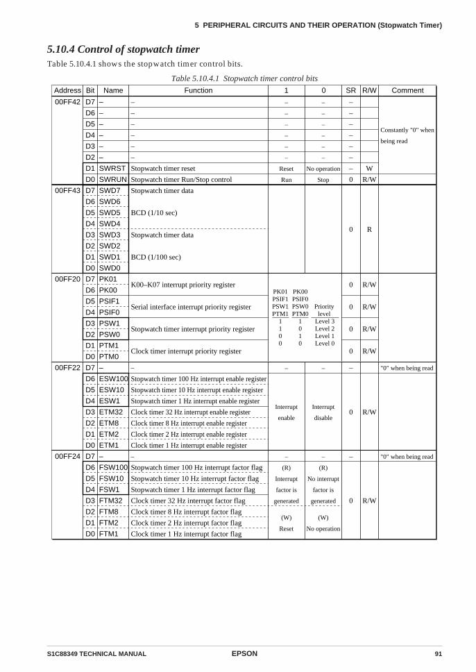
S1C88349 TECHNICAL MANUAL EPSON 91
5 PERIPHERAL CIRCUITS AND THEIR OPERATION (Stopwatch Timer)
5.10.4 Control of stopwatch timerTable 5.10.4.1 shows the stopwatch timer control bits.
Table 5.10.4.1 Stopwatch timer control bits
Address Bit Name
00FF42 D7
D6
D5
D4
D3
D2
D1
D0
–
–
–
–
–
–
SWRST
SWRUN
SR R/WFunction Comment
–
–
–
–
–
–
Stopwatch timer reset
Stopwatch timer Run/Stop control
Constantly "0" when
being read
1 0
–
–
–
–
–
–
–
0
W
R/W
–
–
–
–
–
–
Reset
Run
–
–
–
–
–
–
No operation
Stop
00FF43 D7
D6
D5
D4
D3
D2
D1
D0
SWD7
SWD6
SWD5
SWD4
SWD3
SWD2
SWD1
SWD0
Stopwatch timer data
BCD (1/10 sec)
Stopwatch timer data
BCD (1/100 sec)
0 R
00FF20 D7
D6
D5
D4
D3
D2
D1
D0
PK01
PK00
PSIF1
PSIF0
PSW1
PSW0
PTM1
PTM0
K00–K07 interrupt priority register
Serial interface interrupt priority register
Stopwatch timer interrupt priority register
Clock timer interrupt priority register
0
0
0
0
R/W
R/W
R/W
R/W
PK01PSIF1PSW1PTM1
1100
PK00PSIF0PSW0PTM0
1010
Prioritylevel
Level 3Level 2Level 1Level 0
00FF22 D7
D6
D5
D4
D3
D2
D1
D0
–
ESW100
ESW10
ESW1
ETM32
ETM8
ETM2
ETM1
–
Stopwatch timer 100 Hz interrupt enable register
Stopwatch timer 10 Hz interrupt enable register
Stopwatch timer 1 Hz interrupt enable register
Clock timer 32 Hz interrupt enable register
Clock timer 8 Hz interrupt enable register
Clock timer 2 Hz interrupt enable register
Clock timer 1 Hz interrupt enable register
"0" when being read–
0 R/W
–
Interrupt
enable
–
Interrupt
disable
00FF24 D7
D6
D5
D4
D3
D2
D1
D0
–
FSW100
FSW10
FSW1
FTM32
FTM8
FTM2
FTM1
–
Stopwatch timer 100 Hz interrupt factor flag
Stopwatch timer 10 Hz interrupt factor flag
Stopwatch timer 1 Hz interrupt factor flag
Clock timer 32 Hz interrupt factor flag
Clock timer 8 Hz interrupt factor flag
Clock timer 2 Hz interrupt factor flag
Clock timer 1 Hz interrupt factor flag
"0" when being read–
0 R/W
–
(R)
Interrupt
factor is
generated
(W)
Reset
–
(R)
No interrupt
factor is
generated
(W)
No operation
92 EPSON S1C88349 TECHNICAL MANUAL
5 PERIPHERAL CIRCUITS AND THEIR OPERATION (Stopwatch Timer)
SWD0–SWD7: 00FF43HThe stopwatch timer data can be read out.Higher and lower nibbles and BCD digit corre-spondence are as follows:
SWD0–SWD3: BCD (1/100 sec)SWD4–SWD7: BCD (1/10 sec)
Since SWD0–SWD7 are exclusively for reading, thewrite operation is invalid.At initial reset, the timer data is set to "00H".
SWRST: 00FF42H•D1Resets the stopwatch timer.
When "1" is written: Stopwatch timer resetWhen "0" is written: No operationReading: Always "0"
The stopwatch timer is reset by writing "1" to theSWRST. When the stopwatch timer is reset in theRUN status, it restarts immediately after resetting.In the case of the STOP status, the reset data "00H"is maintained.No operation results when "0" is written to theSWRST.Since the SWRST is exclusively for writing, italways becomes "0" during reading.
SWRUN: 00FF42H•D0Controls RUN/STOP of the stopwatch timer.
When "1" is written: RUNWhen "0" is written: STOPReading: Valid
The stopwatch timer starts up-counting by writing"1" to the SWRUN and stops by writing "0".In the STOP status, the timer data is maintaineduntil it is reset or set in the next RUN status. Also,when the STOP status changes to the RUN status,the data that was maintained can be used forresuming the count.At initial reset, the SWRUN is set at "0" (STOP).
PSW0, PSW1: 00FF20H•D2, D3Sets the priority level of the stopwatch timerinterrupt.The two bits PSW0 and PSW1 are the interruptpriority register corresponding to the stopwatchtimer interrupt. Table 5.10.4.2 shows the interruptpriority level which can be set by this register.
Table 5.10.4.2 Interrupt priority level settings
At initial reset, this register is set to "0" (level 0).
PSW1 PSW0 Interrupt priority level
1
1
0
0
1
0
1
0
Level 3 (IRQ3)
Level 2 (IRQ2)
Level 1 (IRQ1)
Level 0 (None)
ESW1, ESW10, ESW100: 00FF22H•D4, D5, D6Enables or disables the generation of an interruptfor the CPU.
When "1" is written: Interrupt enabledWhen "0" is written: Interrupt disabledReading: Valid
The ESW1, ESW10 and ESW100 are interruptenable registers that respectively correspond to theinterrupt factors for 1 Hz, 10 Hz and 100 Hz.Interrupts set to "1" are enabled and interrupts setto "0" are disabled.At initial reset, this register is set to "0" (interruptdisabled).
FSW1, FSW10, FSW100: 00FF24H•D4, D5, D6Indicates the stopwatch timer interrupt generationstatus.
When "1" is read: Interrupt factor presentWhen "0" is read: Interrupt factor not present
When "1" is written: Resets factor flagWhen "0" is written: Invalid
The FSW1, FSW10 and FSW100 are interrupt factorflags that respectively correspond to the interruptsfor 1 Hz, 10 Hz and 100 Hz and are set to "1" insynchronization with the falling edge of each signal.When set in this manner, if the correspondinginterrupt enable register is set to "1" and thecorresponding interrupt priority register is set to ahigher level than the setting of interrupt flags (I0and I1), an interrupt will be generated to the CPU.Regardless of the interrupt enable register andinterrupt priority register settings, the interruptfactor flag will be set to "1" by the occurrence of aninterrupt generation condition.To accept the subsequent interrupt after interruptgeneration, re-setting of the interrupt flags (setinterrupt flag to lower level than the level indicatedby the interrupt priority registers, or execute theRETE instruction) and interrupt factor flag reset arenecessary. The interrupt factor flag is reset to "0" bywriting "1".At initial reset, this flag is reset to "0".
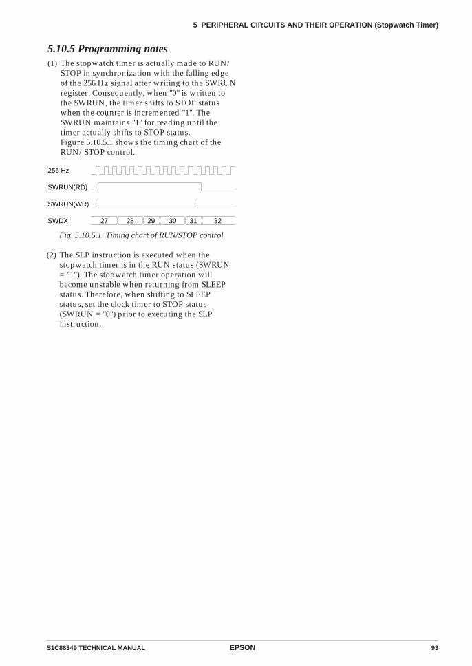
S1C88349 TECHNICAL MANUAL EPSON 93
5 PERIPHERAL CIRCUITS AND THEIR OPERATION (Stopwatch Timer)
5.10.5 Programming notes(1) The stopwatch timer is actually made to RUN/
STOP in synchronization with the falling edgeof the 256 Hz signal after writing to the SWRUNregister. Consequently, when "0" is written tothe SWRUN, the timer shifts to STOP statuswhen the counter is incremented "1". TheSWRUN maintains "1" for reading until thetimer actually shifts to STOP status.Figure 5.10.5.1 shows the timing chart of theRUN/STOP control.
SWRUN(WR)
SWDX 27 28 29 30 31 32
SWRUN(RD)
256 Hz
Fig. 5.10.5.1 Timing chart of RUN/STOP control
(2) The SLP instruction is executed when thestopwatch timer is in the RUN status (SWRUN= "1"). The stopwatch timer operation willbecome unstable when returning from SLEEPstatus. Therefore, when shifting to SLEEPstatus, set the clock timer to STOP status(SWRUN = "0") prior to executing the SLPinstruction.

94 EPSON S1C88349 TECHNICAL MANUAL
5 PERIPHERAL CIRCUITS AND THEIR OPERATION (Programmable Timer)
5.11 Programmable Timer
5.11.1 Configuration of programmable timerThe S1C88349 has two built-in 8-bit programmabletimer systems (timer 0 and timer 1).Timer 0 and timer 1 are composed of 8-bitpresettable down counters and they can be used as8-bit × 2 channels or 16-bit × 1 channel programma-ble timer. They also have an event counter functionand a pulse width measurement function using theK10 input port terminal.Figure 5.11.1.1 shows the configuration of theprogrammable timer.
Programmable setting of the transfer rate is possi-ble, due to the fact that the programmable timerunderflow signal can be used as a synchronousclock for the serial interface.The underflow divided by 1/2 signal can also beoutput externally from the R27 output port terminal.
5.11.2 Count operation andsetting basic mode
Here we will explain the basic operation andsetting of the programmable timer.
Setting of initial value and counting downThe timers 0 and 1 each have a down counter andreload data register.
The reload data registers RLD00–RLD07 (timer 0)and RLD10–RLD17 (timer 1) are registers that setthe initial value of the counter.By writing "1" to the preset control bit PSET0 (timer0) or PSET1 (timer 1), the down counter loads theinitial value set in the reload register RLD.Therefore, down-counting is executed from thestored initial value according to the input clock.
Fig. 5.11.1.1 Configuration of programmable timer
Reload data registerRLD00–RLD07
Data bufferPTD00–PTD07
Input portK10
PRUN0
FCSEL
PLPOL
Programmable timer 0
PSC00PSC01
Reloadsignal
8-bit down counterPrescaler
OSC3oscillationcircuit
OSC1oscillationcircuit Selector
CKSEL0
Timer 0 Run/Stop
EVIN (K10)
RLMD0
PSET0
Clockcontroller
Reloadcontroller
EVCNTEvent counter mode setting
Timer function setting
Pulse polarity setting
Prescalersetting
Underflowsignal
Reload data registerRLD10–RLD17
Data bufferPTD10–PTD17
MODE16
Programmable timer 1
PSC10PSC11
Reloadsignal
8-bit down counterPrescaler
RLMD1
PSET1
Clockcontroller
Reloadcontroller
8/16-bit modesetting
Prescalersetting
Underflowsignal
Dat
a bu
sInterruptrequest
Interruptcontrolcircuit
Output portR27TOUT (R27)
Serialinterface
PRUN1
Selector
CKSEL1
Timer 1 Run/Stop
fOSC1
fOSC3
Divider2,048 Hz
Selector
CHSEL
1/2
PTOUT

S1C88349 TECHNICAL MANUAL EPSON 95
5 PERIPHERAL CIRCUITS AND THEIR OPERATION (Programmable Timer)
Fig. 5.11.2.1 Basic operation timing of the counter
Fig. 5.11.2.2 Continuous mode and one-shot mode
Continuous/one-shot mode settingBy writing "1" to the continuous/one-shot modeselection registers CONT0 (timer 0) and CONT1(timer 1), the programmable timer is set to thecontinuous mode. In the continuous mode, theinitial counter value is automatically loaded whenan underflow is generated, and counting is contin-ued. This mode is suitable when programmableintervals are necessary (such as an interrupt and asynchronous clock for the serial interface).On the other hand, when writing "0" to the registersCONT0 (timer 0) and CONT1 (timer 1), the pro-grammable timer is set to the one-shot mode. Thecounter loads an initial value and stops when anunderflow is generated. At this time, the RUN/STOP control register PRUN0 (timer 0) and PRUN1(timer 1) are automatically reset to "0". After thecounter stops, a one-shot count can be performedonce again by writing "1" to registers PRUN0 (timer0) and PRUN1 (timer 1). This mode is suitable forsingle time measurement, for example.
The registers PRUN0 (timer 0) and PRUN1 (timer 1)are provided to control the RUN/STOP for timers 0and 1.After the reload data has been preset into thecounter, down-counting is begun by writing "1" tothis register. When "0" is written, the clock input isprohibited and the count stops.The control of this RUN/STOP has no affect on thecounter data. The counter data is maintained evenduring the stoppage of the counter and it can startthe count, continuing from that data.
The reading of the counter data can be donethrough the data buffers PTD00–PTD07 (timer 0)and PTD10–PTD17 (timer 1) with optional timing.When the down-counting has progressed and anunderflow is generated, the counter reloads theinitial value set in the reload data register.This underflow signal controls an interrupt genera-tion, pulse (TOUT signal) output and serial inter-face clocking, in addition to reloading the counter.
PRUN0(1)
PSET0(1)
RLD00–07(10–17)
Input clock
PTD07(17)
PTD06(16)
PTD05(15)
PTD04(14)
PTD03(13)
PTD02(12)
PTD01(11)
PTD00(10)
A6H F3H
PresetReload andinterrupt generation
Input clock
Underflow
ContinuousmodeOne-shotmode
03H 02H 01H 00H A6H A5H A4H
03H 02H 01H 00H A6H
Countdata
When "A6H" is set into reload data register RLD.
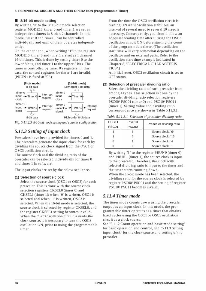
96 EPSON S1C88349 TECHNICAL MANUAL
5 PERIPHERAL CIRCUITS AND THEIR OPERATION (Programmable Timer)
8/16-bit mode settingBy writing "0" to the 8/16-bit mode selectionregister MODE16, timer 0 and timer 1 are set asindependent timers in 8-bit × 2 channels. In thismode, timer 0 and timer 1 can be controlledindividually and each of them operates independ-ently.On the other hand, when writing "1" to the registerMODE16, timer 0 and timer1 are set as 1 channel16-bit timer. This is done by setting timer 0 to thelower 8 bits, and timer 1 to the upper 8 bits. Thetimer is controlled by timer 0's registers. In thiscase, the control registers for timer 1 are invalid.(PRUN1 is fixed at "0".)
From the time the OSC3 oscillation circuit isturning ON until oscillation stabilizes, aninterval of several msec to several 10 msec isnecessary. Consequently, you should allow anadequate waiting time after turning the OSC3oscillation circuit ON before starting the countof the programmable timer. (The oscillationstart time will vary somewhat depending on theoscillator and on external parts. Refer to theoscillation start time example indicated inChapter 8, "ELECTRICAL CHARACTERIS-TICS".)At initial reset, OSC3 oscillation circuit is set toOFF status.
(2) Selection of prescaler dividing ratioSelect the dividing ratio of each prescaler fromamong 4 types. This selection is done by theprescaler dividing ratio selection registersPSC00/PSC01 (timer 0) and PSC10/PSC11(timer 1). Setting value and dividing ratiocorrespondence are shown in Table 5.11.3.1.
Table 5.11.3.1 Selection of prescaler dividing ratio
Fig. 5.11.2.3 8/16-bit mode setting and counter configuration
5.11.3 Setting of input clockPrescalers have been provided for timers 0 and 1.The prescalers generate the input clock for each bydividing the source clock signal from the OSC1 orOSC3 oscillation circuit.The source clock and the dividing ratio of theprescaler can be selected individually for timer 0and timer 1 in software.
The input clocks are set by the below sequence.
(1) Selection of source clockSelect the source clock (OSC1 or OSC3) for eachprescaler. This is done with the source clockselection registers CKSEL0 (timer 0) andCKSEL1 (timer 1): when "0" is written, OSC1 isselected and when "1" is written, OSC3 isselected. When the 16-bit mode is selected, thesource clock is selected by register CKSEL0, andthe register CKSEL1 setting becomes invalid.When the OSC3 oscillation circuit is made theclock source, it is necessary to turn the OSC3oscillation ON, prior to using the programmabletimer.
By writing "1" to the register PRUN0 (timer 0)and PRUN1 (timer 1), the source clock is inputto the prescaler. Therefore, the clock withselected dividing ratio is input to the timer andthe timer starts counting down.When the 16-bit mode has been selected, thedividing ratio for the source clock is selected byregister PSC00/PSC01 and the setting of registerPSC10/PSC11 becomes invalid.
5.11.4 Timer modeThe timer mode counts down using the prescaleroutput as an input clock. In this mode, the pro-grammable timer operates as a timer that obtainsfixed cycles using the OSC1 or OSC3 oscillationcircuit as a clock source.See "5.11.2 Count operation and basic mode setting"for basic operation and control, and "5.11.3 Settinginput clock" for the clock source and setting of theprescaler.
8-bit data
8-bit data
Timer 0
Timer 1
Timer 0inputclock
Timer 1inputclock
Low-order 8-bit data
High-order 8-bit data
Timer 0
Timer 1
Timer 0inputclock
Timer 0underflowsignal
Interruptrequest
[16-bit mode]
Interruptrequest
Interruptrequest
[8-bit mode]
PSC11
PSC01
PSC10
PSC00Prescaler dividing ratio
1
1
0
0
1
0
1
0
Source clock / 64
Source clock / 16
Source clock / 4
Source clock / 1
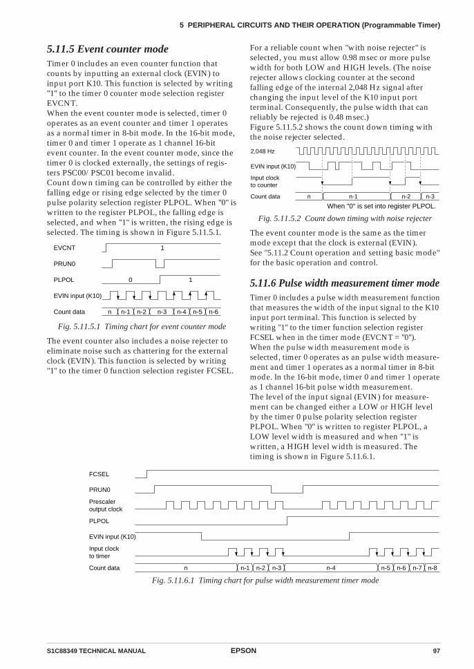
S1C88349 TECHNICAL MANUAL EPSON 97
5 PERIPHERAL CIRCUITS AND THEIR OPERATION (Programmable Timer)
5.11.5 Event counter modeTimer 0 includes an even counter function thatcounts by inputting an external clock (EVIN) toinput port K10. This function is selected by writing"1" to the timer 0 counter mode selection registerEVCNT.When the event counter mode is selected, timer 0operates as an event counter and timer 1 operatesas a normal timer in 8-bit mode. In the 16-bit mode,timer 0 and timer 1 operate as 1 channel 16-bitevent counter. In the event counter mode, since thetimer 0 is clocked externally, the settings of regis-ters PSC00/PSC01 become invalid.Count down timing can be controlled by either thefalling edge or rising edge selected by the timer 0pulse polarity selection register PLPOL. When "0" iswritten to the register PLPOL, the falling edge isselected, and when "1" is written, the rising edge isselected. The timing is shown in Figure 5.11.5.1.
For a reliable count when "with noise rejecter" isselected, you must allow 0.98 msec or more pulsewidth for both LOW and HIGH levels. (The noiserejecter allows clocking counter at the secondfalling edge of the internal 2,048 Hz signal afterchanging the input level of the K10 input portterminal. Consequently, the pulse width that canreliably be rejected is 0.48 msec.)Figure 5.11.5.2 shows the count down timing withthe noise rejecter selected.
Input clockto counter
Count data n n-1 n-2 n-3
EVIN input (K10)
2,048 Hz
When "0" is set into register PLPOL.
Fig. 5.11.5.2 Count down timing with noise rejecter
The event counter mode is the same as the timermode except that the clock is external (EVIN).See "5.11.2 Count operation and setting basic mode"for the basic operation and control.
5.11.6 Pulse width measurement timer modeTimer 0 includes a pulse width measurement functionthat measures the width of the input signal to the K10input port terminal. This function is selected bywriting "1" to the timer function selection registerFCSEL when in the timer mode (EVCNT = "0").When the pulse width measurement mode isselected, timer 0 operates as an pulse width measure-ment and timer 1 operates as a normal timer in 8-bitmode. In the 16-bit mode, timer 0 and timer 1 operateas 1 channel 16-bit pulse width measurement.The level of the input signal (EVIN) for measure-ment can be changed either a LOW or HIGH levelby the timer 0 pulse polarity selection registerPLPOL. When "0" is written to register PLPOL, aLOW level width is measured and when "1" iswritten, a HIGH level width is measured. Thetiming is shown in Figure 5.11.6.1.
EVIN input (K10)
Count data n n-1 n-2 n-3 n-4 n-5 n-6
PLPOL
EVCNT
0 1
1
PRUN0
Fig. 5.11.5.1 Timing chart for event counter mode
The event counter also includes a noise rejecter toeliminate noise such as chattering for the externalclock (EVIN). This function is selected by writing"1" to the timer 0 function selection register FCSEL.
EVIN input (K10)
Count data
PLPOL
Prescaleroutput clock
n n-1 n-2 n-3 n-4
Input clockto timer
PRUN0
FCSEL
n-5 n-6 n-7 n-8
Fig. 5.11.6.1 Timing chart for pulse width measurement timer mode
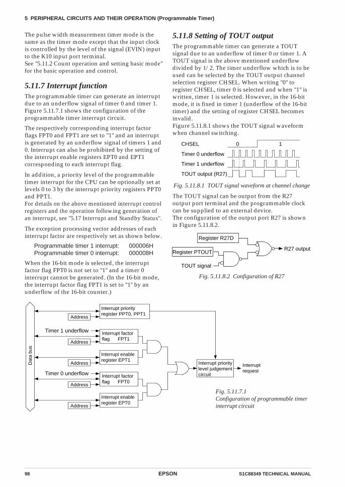
98 EPSON S1C88349 TECHNICAL MANUAL
5 PERIPHERAL CIRCUITS AND THEIR OPERATION (Programmable Timer)
The pulse width measurement timer mode is thesame as the timer mode except that the input clockis controlled by the level of the signal (EVIN) inputto the K10 input port terminal.See "5.11.2 Count operation and setting basic mode"for the basic operation and control.
5.11.7 Interrupt functionThe programmable timer can generate an interruptdue to an underflow signal of timer 0 and timer 1.Figure 5.11.7.1 shows the configuration of theprogrammable timer interrupt circuit.
5.11.8 Setting of TOUT outputThe programmable timer can generate a TOUTsignal due to an underflow of timer 0 or timer 1. ATOUT signal is the above mentioned underflowdivided by 1/2. The timer underflow which is to beused can be selected by the TOUT output channelselection register CHSEL. When writing "0" toregister CHSEL, timer 0 is selected and when "1" iswritten, timer 1 is selected. However, in the 16-bitmode, it is fixed in timer 1 (underflow of the 16-bittimer) and the setting of register CHSEL becomesinvalid.Figure 5.11.8.1 shows the TOUT signal waveformwhen channel switching.
The respectively corresponding interrupt factorflags FPT0 and FPT1 are set to "1" and an interruptis generated by an underflow signal of timers 1 and0. Interrupt can also be prohibited by the setting ofthe interrupt enable registers EPT0 and EPT1corresponding to each interrupt flag.
In addition, a priority level of the programmabletimer interrupt for the CPU can be optionally set atlevels 0 to 3 by the interrupt priority registers PPT0and PPT1.For details on the above mentioned interrupt controlregisters and the operation following generation ofan interrupt, see "5.17 Interrupt and Standby Status".
The exception processing vector addresses of eachinterrupt factor are respectively set as shown below.
Programmable timer 1 interrupt: 000006HProgrammable timer 0 interrupt: 000008H
When the 16-bit mode is selected, the interruptfactor flag FPT0 is not set to "1" and a timer 0interrupt cannot be generated. (In the 16-bit mode,the interrupt factor flag FPT1 is set to "1" by anunderflow of the 16-bit counter.)
Timer 0 underflow
Timer 1 underflow
CHSEL 0 1
TOUT output (R27)
Fig. 5.11.8.1 TOUT signal waveform at channel change
The TOUT signal can be output from the R27output port terminal and the programmable clockcan be supplied to an external device.The configuration of the output port R27 is shownin Figure 5.11.8.2.
Register R27D
Register PTOUTR27 output
TOUT signal
Fig. 5.11.8.2 Configuration of R27
Dat
a bu
s
Interruptrequest
Address
Timer 1 underflow Interrupt factorflag FPT1
Address
Interrupt enableregister EPT1
Address
Timer 0 underflow Interrupt factorflag FPT0
Address
Interrupt enableregister EPT0
Interrupt prioritylevel judgementcircuit
Address
Interrupt priority register PPT0, PPT1
Fig. 5.11.7.1Configuration of programmable timerinterrupt circuit
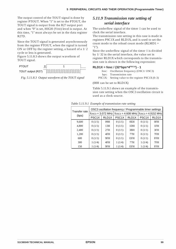
S1C88349 TECHNICAL MANUAL EPSON 99
5 PERIPHERAL CIRCUITS AND THEIR OPERATION (Programmable Timer)
PTOUT
TOUT output (R27)
0 1
Fig. 5.11.8.3 Output waveform of the TOUT signal
5.11.9 Transmission rate setting ofserial interface
The underflow signal of the timer 1 can be used toclock the serial interface.The transmission rate setting in this case is made inregisters PSC1X and RLD1X, and is used to set thecount mode to the reload count mode (RLMD1 ="1").Since the underflow signal of the timer 1 is dividedby 1/32 in the serial interface, the value set inregister RLD1X which corresponds to the transmis-sion rate is shown in the following expression:
RLD1X = fosc / (32*bps*4PSC1X) - 1fosc: Oscillation frequency (OSC1/OSC3)bps: Transmission rate
PSC1X: Setting value to the register PSC1X (0–3)
(00H can be set to RLD1X)
Table 5.11.9.1 shows an example of the transmis-sion rate setting when the OSC3 oscillation circuit isused as a clock source.
Table 5.11.9.1 Example of transmission rate setting
The output control of the TOUT signal is done byregister PTOUT. When "1" is set to the PTOUT, theTOUT signal is output from the R27 output portand when "0" is set, HIGH (VDD) level is output. Atthis time, "1" must always be set in the data registerR27D.
Since the TOUT signal is generated asynchronouslyfrom the register PTOUT, when the signal is turnedON or OFF by the register setting, a hazard of a 1/2cycle or less is generated.Figure 5.11.8.3 shows the output waveform ofTOUT signal.
Transfer rate
(bps)
9,600
4,800
2,400
1,200
600
300
150
OSC3 oscillation frequency / Programmable timer settings
fOSC3 = 3.072 MHz
PSC1X
0 (1/1)
0 (1/1)
0 (1/1)
0 (1/1)
0 (1/1)
1 (1/4)
1 (1/4)
RLD1X
09H
13H
27H
4FH
9FH
4FH
9FH
fOSC3 = 4.608 MHz
PSC1X
0 (1/1)
0 (1/1)
0 (1/1)
0 (1/1)
0 (1/1)
1 (1/4)
1 (1/4)
RLD1X
0EH
1DH
3BH
77H
EFH
77H
EFH
fOSC3 = 4.9152 MHz
PSC1X
0 (1/1)
0 (1/1)
0 (1/1)
0 (1/1)
0 (1/1)
1 (1/4)
1 (1/4)
RLD1X
0FH
1FH
3FH
7FH
FFH
7FH
FFH
100 EPSON S1C88349 TECHNICAL MANUAL
5 PERIPHERAL CIRCUITS AND THEIR OPERATION (Programmable Timer)
5.11.10 Control of programmable timerTable 5.11.10.1 shows the programmable timer control bits.
Table 5.11.10.1(a) Programmable timer control bits
Address Bit Name
00FF30 D7
D6
D5
D4
D3
D2
D1
D0
–
–
–
MODE16
CHSEL
PTOUT
CKSEL1
CKSEL0
SR R/WFunction Comment
–
–
–
8/16-bit mode selection
TOUT output channel selection
TOUT output control
Prescaler 1 source clock selection
Prescaler 0 source clock selection
Constantly "0" when
being read
1 0
–
–
–
0
0
0
0
0
R/W
R/W
R/W
R/W
R/W
–
–
–
16-bit x 1
Timer 1
On
fOSC3
fOSC3
–
–
–
8-bit x 2
Timer 0
Off
fOSC1
fOSC1
00FF31 D7
D6
D5
D4
D3
D2
D1
D0
EVCNT
FCSEL
PLPOL
PSC01
PSC00
CONT0
PSET0
PRUN0
Timer 0 counter mode selection
Timer 0
function selection
Timer 0
pulse polarity
selection
Timer 0 prescaler dividing ratio selection
Timer 0 continuous/one-shot mode selection
Timer 0 preset
Timer 0 Run/Stop control
"0" when being read
0
0
0
0
0
0
–
0
R/W
R/W
R/W
R/W
R/W
R/W
W
R/W
Event counter
Pulse width
measurement
With
noise rejector
Rising edge
of K10 inputHigh level
measurementfor K10 input
Continuous
Preset
Run
Timer
Normal
mode
Without
noise rejector
Falling edge
of K10 inputLow level
measurementfor K10 input
One-shot
No operation
Stop
In timer mode
In event counter mode
Down count timing
in event counter mode
In pulse width
measurement mode
PSC01
1
1
0
0
PSC00
1
0
1
0
Prescaler dividing ratio
Source clock / 64
Source clock / 16
Source clock / 4
Source clock / 1
00FF32 D7
D6
D5
D4
D3
D2
D1
D0
–
–
–
PSC11
PSC10
CONT1
PSET1
PRUN1
–
–
–
Timer 1 prescaler dividing ratio selection
Timer 1 continuous/one-shot mode selection
Timer 1 preset
Timer 1 Run/Stop control
Constantly "0" when
being read
"0" when being read
–
–
–
0
0
0
–
0
R/W
R/W
R/W
W
R/W
–
–
–
One-shot
No operation
Stop
PSC11
1
1
0
0
PSC10
1
0
1
0
Prescaler dividing ratio
Source clock / 64
Source clock / 16
Source clock / 4
Source clock / 1
–
–
–
Continuous
Preset
Run
D7
D6
D5
D4
D3
D2
D1
D0
RLD07
RLD06
RLD05
RLD04
RLD03
RLD02
RLD01
RLD00
Timer 0 reload data D7 (MSB)
Timer 0 reload data D6
Timer 0 reload data D5
Timer 0 reload data D4
Timer 0 reload data D3
Timer 0 reload data D2
Timer 0 reload data D1
Timer 0 reload data D0 (LSB)
1 R/WHigh Low
00FF33
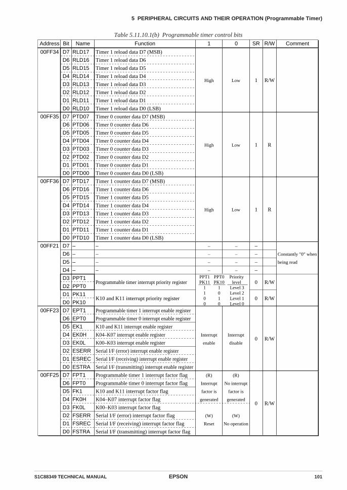
S1C88349 TECHNICAL MANUAL EPSON 101
5 PERIPHERAL CIRCUITS AND THEIR OPERATION (Programmable Timer)
Table 5.11.10.1(b) Programmable timer control bits
Address Bit Name SR R/WFunction Comment1 0
D7
D6
D5
D4
D3
D2
D1
D0
RLD17
RLD16
RLD15
RLD14
RLD13
RLD12
RLD11
RLD10
Timer 1 reload data D7 (MSB)
Timer 1 reload data D6
Timer 1 reload data D5
Timer 1 reload data D4
Timer 1 reload data D3
Timer 1 reload data D2
Timer 1 reload data D1
Timer 1 reload data D0 (LSB)
1 R/WHigh Low
00FF34
D7
D6
D5
D4
D3
D2
D1
D0
PTD07
PTD06
PTD05
PTD04
PTD03
PTD02
PTD01
PTD00
Timer 0 counter data D7 (MSB)
Timer 0 counter data D6
Timer 0 counter data D5
Timer 0 counter data D4
Timer 0 counter data D3
Timer 0 counter data D2
Timer 0 counter data D1
Timer 0 counter data D0 (LSB)
1 RHigh Low
00FF35
D7
D6
D5
D4
D3
D2
D1
D0
PTD17
PTD16
PTD15
PTD14
PTD13
PTD12
PTD11
PTD10
Timer 1 counter data D7 (MSB)
Timer 1 counter data D6
Timer 1 counter data D5
Timer 1 counter data D4
Timer 1 counter data D3
Timer 1 counter data D2
Timer 1 counter data D1
Timer 1 counter data D0 (LSB)
1 RHigh Low
00FF36
00FF21 D7
D6
D5
D4
D3
D2
D1
D0
–
–
–
–
PPT1
PPT0
PK11
PK10
–
–
–
–
Programmable timer interrupt priority register
K10 and K11 interrupt priority register
Constantly "0" when
being read
–
–
–
–
0
0
R/W
R/W
–
–
–
–
–
–
–
–PPT1PK11
1100
PPT0PK10
1010
Prioritylevel
Level 3Level 2Level 1Level 0
D7
D6
D5
D4
D3
D2
D1
D0
00FF25 D7
D6
D5
D4
D3
D2
D1
D0
FPT1
FPT0
FK1
FK0H
FK0L
FSERR
FSREC
FSTRA
Programmable timer 1 interrupt factor flag
Programmable timer 0 interrupt factor flag
K10 and K11 interrupt factor flag
K04–K07 interrupt factor flag
K00–K03 interrupt factor flag
Serial I/F (error) interrupt factor flag
Serial I/F (receiving) interrupt factor flag
Serial I/F (transmitting) interrupt factor flag
0 R/W
(R)
Interrupt
factor is
generated
(W)
Reset
(R)
No interrupt
factor is
generated
(W)
No operation
00FF23 EPT1
EPT0
EK1
EK0H
EK0L
ESERR
ESREC
ESTRA
Programmable timer 1 interrupt enable register
Programmable timer 0 interrupt enable register
K10 and K11 interrupt enable register
K04–K07 interrupt enable register
K00–K03 interrupt enable register
Serial I/F (error) interrupt enable register
Serial I/F (receiving) interrupt enable register
Serial I/F (transmitting) interrupt enable register
0 R/WInterrupt
enable
Interrupt
disable
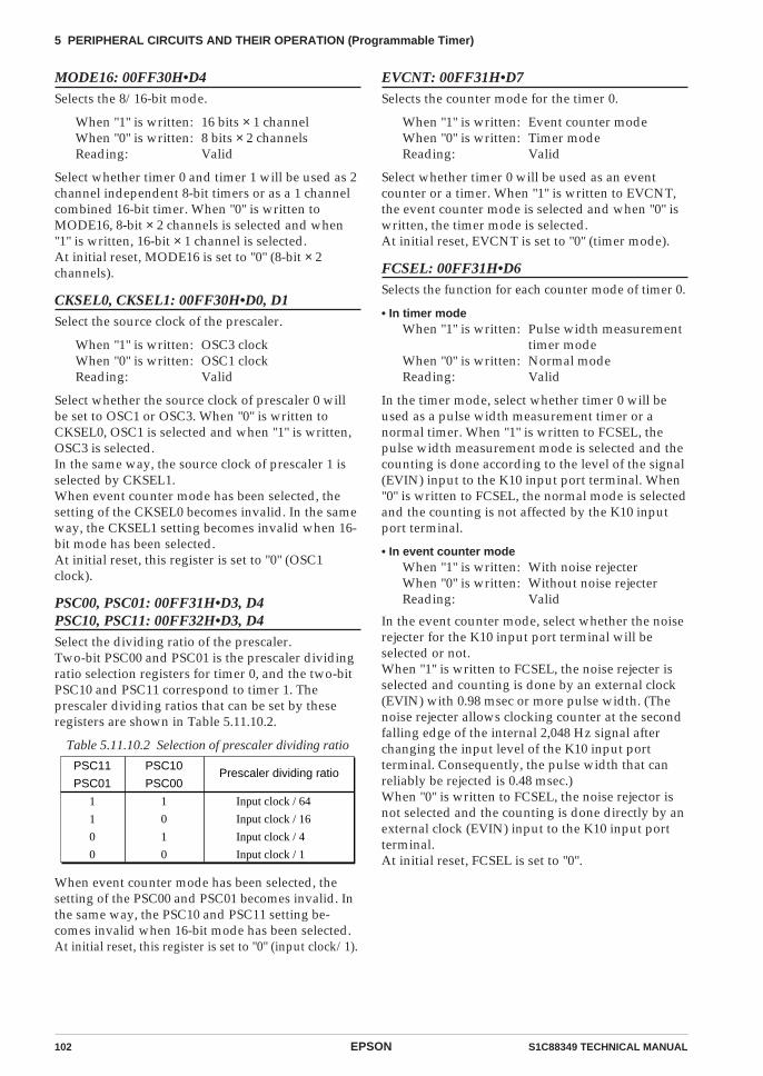
102 EPSON S1C88349 TECHNICAL MANUAL
5 PERIPHERAL CIRCUITS AND THEIR OPERATION (Programmable Timer)
PSC11
PSC01
PSC10
PSC00Prescaler dividing ratio
1
1
0
0
1
0
1
0
Input clock / 64
Input clock / 16
Input clock / 4
Input clock / 1
MODE16: 00FF30H•D4Selects the 8/16-bit mode.
When "1" is written: 16 bits × 1 channelWhen "0" is written: 8 bits × 2 channelsReading: Valid
Select whether timer 0 and timer 1 will be used as 2channel independent 8-bit timers or as a 1 channelcombined 16-bit timer. When "0" is written toMODE16, 8-bit × 2 channels is selected and when"1" is written, 16-bit × 1 channel is selected.At initial reset, MODE16 is set to "0" (8-bit × 2channels).
CKSEL0, CKSEL1: 00FF30H•D0, D1Select the source clock of the prescaler.
When "1" is written: OSC3 clockWhen "0" is written: OSC1 clockReading: Valid
Select whether the source clock of prescaler 0 willbe set to OSC1 or OSC3. When "0" is written toCKSEL0, OSC1 is selected and when "1" is written,OSC3 is selected.In the same way, the source clock of prescaler 1 isselected by CKSEL1.When event counter mode has been selected, thesetting of the CKSEL0 becomes invalid. In the sameway, the CKSEL1 setting becomes invalid when 16-bit mode has been selected.At initial reset, this register is set to "0" (OSC1clock).
PSC00, PSC01: 00FF31H•D3, D4PSC10, PSC11: 00FF32H•D3, D4Select the dividing ratio of the prescaler.Two-bit PSC00 and PSC01 is the prescaler dividingratio selection registers for timer 0, and the two-bitPSC10 and PSC11 correspond to timer 1. Theprescaler dividing ratios that can be set by theseregisters are shown in Table 5.11.10.2.
Table 5.11.10.2 Selection of prescaler dividing ratio
EVCNT: 00FF31H•D7Selects the counter mode for the timer 0.
When "1" is written: Event counter modeWhen "0" is written: Timer modeReading: Valid
Select whether timer 0 will be used as an eventcounter or a timer. When "1" is written to EVCNT,the event counter mode is selected and when "0" iswritten, the timer mode is selected.At initial reset, EVCNT is set to "0" (timer mode).
FCSEL: 00FF31H•D6Selects the function for each counter mode of timer 0.
• In timer modeWhen "1" is written: Pulse width measurement
timer modeWhen "0" is written: Normal modeReading: Valid
In the timer mode, select whether timer 0 will beused as a pulse width measurement timer or anormal timer. When "1" is written to FCSEL, thepulse width measurement mode is selected and thecounting is done according to the level of the signal(EVIN) input to the K10 input port terminal. When"0" is written to FCSEL, the normal mode is selectedand the counting is not affected by the K10 inputport terminal.
• In event counter modeWhen "1" is written: With noise rejecterWhen "0" is written: Without noise rejecterReading: Valid
In the event counter mode, select whether the noiserejecter for the K10 input port terminal will beselected or not.When "1" is written to FCSEL, the noise rejecter isselected and counting is done by an external clock(EVIN) with 0.98 msec or more pulse width. (Thenoise rejecter allows clocking counter at the secondfalling edge of the internal 2,048 Hz signal afterchanging the input level of the K10 input portterminal. Consequently, the pulse width that canreliably be rejected is 0.48 msec.)When "0" is written to FCSEL, the noise rejector isnot selected and the counting is done directly by anexternal clock (EVIN) input to the K10 input portterminal.At initial reset, FCSEL is set to "0".
When event counter mode has been selected, thesetting of the PSC00 and PSC01 becomes invalid. Inthe same way, the PSC10 and PSC11 setting be-comes invalid when 16-bit mode has been selected.At initial reset, this register is set to "0" (input clock/1).
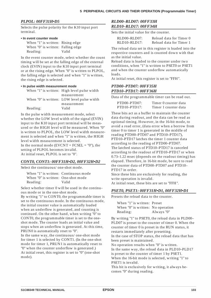
S1C88349 TECHNICAL MANUAL EPSON 103
5 PERIPHERAL CIRCUITS AND THEIR OPERATION (Programmable Timer)
RLD00–RLD07: 00FF33HRLD10–RLD17: 00FF34HSets the initial value for the counter.
RLD00–RLD07: Reload data for Timer 0RLD10–RLD17: Reload data for Timer 1
The reload data set in this register is loaded into therespective counters and is counted down with thatas the initial value.Reload data is loaded to the counter under twoconditions, when "1" is written to PSET0 or PSET1and when the counter underflow automaticallyloads.At initial reset, this register is set to "FFH".
PTD00–PTD07: 00FF35HPTD10–PTD17: 00FF36HData of the programmable timer can be read out.
PTD00–PTD07: Timer 0 counter dataPTD10–PTD17: Timer 1 counter data
These bits act as a buffer to maintain the counterdata during readout, and the data can be read asoptional timing. However, in the 16-bit mode, toavoid a read error, (data error when a borrow fromtimer 0 to timer 1 is generated in the middle ofreading PTD00–PTD07 and PTD10–PTD17),PTD10–PTD17 latches the timer 1 counter dataaccording to the reading of PTD00–PTD07.The latched status of PTD10–PTD17 is canceledaccording to the readout of PTD10–PTD17 or when0.73–1.22 msec (depends on the readout timing) haselapsed. Therefore, in 16-bit mode, be sure to readthe counter data of PTD00–PTD07 and PTD10–PTD17 in order.Since these bits are exclusively for reading, thewrite operation is invalid.At initial reset, these bits are set to "FFH".
PSET0, PSET1: 00FF31H•D1, 00FF32H•D1Presets the reload data to the counter.
When "1" is written: PresetWhen "0" is written: No operationReading: Always "0"
By writing "1" to PSET0, the reload data in PLD00–PLD07 is preset to the counter of timer 0. When thecounter of timer 0 is preset in the RUN status, itrestarts immediately after presetting.In the case of STOP status, the reload data that hasbeen preset is maintained.No operation results when "0" is written.In the same way, the reload data in PLD10–PLD17is preset to the counter of timer 1 by PSET1.When the 16-bit mode is selected, writing "1" toPSET1 is invalid.This bit is exclusively for writing, it always be-comes "0" during reading.
PLPOL: 00FF31H•D5Selects the pulse polarity for the K10 input portterminal.
• In event counter modeWhen "1" is written: Rising edgeWhen "0" is written: Falling edgeReading: Valid
In the event counter mode, select whether the counttiming will be set at the falling edge of the externalclock (EVIN) input to the K10 input port terminalor at the rising edge. When "0" is written to PLPOL,the falling edge is selected and when "1" is written,the rising edge is selected.
• In pulse width measurement modeWhen "1" is written: High level pulse width
measurementWhen "0" is written: LOW level pulse width
measurementReading: Valid
In the pulse width measurement mode, selectwhether the LOW level width of the signal (EVIN)input to the K10 input port terminal will be meas-ured or the HIGH level will be measured. When "0"is written to PLPOL, the LOW level width measure-ment is selected and when "1" is written, the HIGHlevel width measurement is selected.In the normal mode (EVCNT = FCSEL = "0"), thesetting of PLPOL becomes invalid.At initial reset, PLPOL is set to "0".
CONT0, CONT1: 00FF31H•D2, 00FF32H•D2Select the continuous/one-shot mode.
When "1" is written: Continuous modeWhen "0" is written: One-shot modeReading: Valid
Select whether timer 0 will be used in the continu-ous mode or in the one-shot mode.By writing "1" to CONT0, the programmable timer isset to the continuous mode. In the continuous mode,the initial counter value is automatically loadedwhen an underflow is generated, and counting iscontinued. On the other hand, when writing "0" toCONT0, the programmable timer is set to the one-shot mode. The counter loads an initial value andstops when an underflow is generated. At this time,PRUN0 is automatically reset to "0".In the same way, the continuous/one-shot modefor timer 1 is selected by CONT1. (In the one-shotmode for timer 1, PRUN1 is automatically reset to"0" when the counter underflow is generated.)At initial reset, this register is set to "0" (one-shotmode).
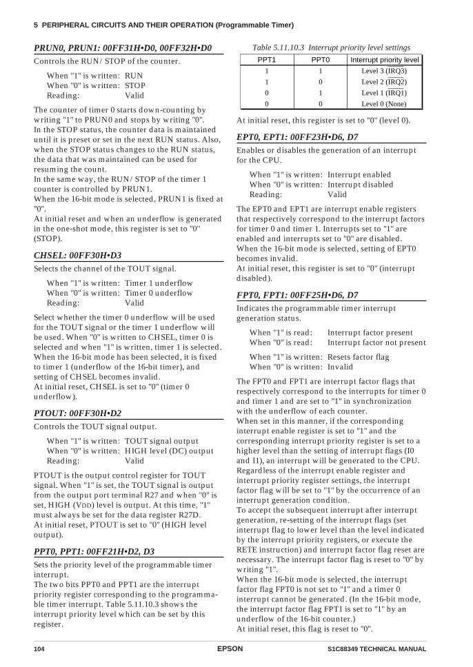
104 EPSON S1C88349 TECHNICAL MANUAL
5 PERIPHERAL CIRCUITS AND THEIR OPERATION (Programmable Timer)
PPT1 PPT0 Interrupt priority level
1
1
0
0
1
0
1
0
Level 3 (IRQ3)
Level 2 (IRQ2)
Level 1 (IRQ1)
Level 0 (None)
PRUN0, PRUN1: 00FF31H•D0, 00FF32H•D0Controls the RUN/STOP of the counter.
When "1" is written: RUNWhen "0" is written: STOPReading: Valid
The counter of timer 0 starts down-counting bywriting "1" to PRUN0 and stops by writing "0".In the STOP status, the counter data is maintaineduntil it is preset or set in the next RUN status. Also,when the STOP status changes to the RUN status,the data that was maintained can be used forresuming the count.In the same way, the RUN/STOP of the timer 1counter is controlled by PRUN1.When the 16-bit mode is selected, PRUN1 is fixed at"0".At initial reset and when an underflow is generatedin the one-shot mode, this register is set to "0"(STOP).
CHSEL: 00FF30H•D3Selects the channel of the TOUT signal.
When "1" is written: Timer 1 underflowWhen "0" is written: Timer 0 underflowReading: Valid
Select whether the timer 0 underflow will be usedfor the TOUT signal or the timer 1 underflow willbe used. When "0" is written to CHSEL, timer 0 isselected and when "1" is written, timer 1 is selected.When the 16-bit mode has been selected, it is fixedto timer 1 (underflow of the 16-bit timer), andsetting of CHSEL becomes invalid.At initial reset, CHSEL is set to "0" (timer 0underflow).
PTOUT: 00FF30H•D2Controls the TOUT signal output.
When "1" is written: TOUT signal outputWhen "0" is written: HIGH level (DC) outputReading: Valid
PTOUT is the output control register for TOUTsignal. When "1" is set, the TOUT signal is outputfrom the output port terminal R27 and when "0" isset, HIGH (VDD) level is output. At this time, "1"must always be set for the data register R27D.At initial reset, PTOUT is set to "0" (HIGH leveloutput).
PPT0, PPT1: 00FF21H•D2, D3Sets the priority level of the programmable timerinterrupt.The two bits PPT0 and PPT1 are the interruptpriority register corresponding to the programma-ble timer interrupt. Table 5.11.10.3 shows theinterrupt priority level which can be set by thisregister.
At initial reset, this register is set to "0" (level 0).
EPT0, EPT1: 00FF23H•D6, D7Enables or disables the generation of an interruptfor the CPU.
When "1" is written: Interrupt enabledWhen "0" is written: Interrupt disabledReading: Valid
The EPT0 and EPT1 are interrupt enable registersthat respectively correspond to the interrupt factorsfor timer 0 and timer 1. Interrupts set to "1" areenabled and interrupts set to "0" are disabled.When the 16-bit mode is selected, setting of EPT0becomes invalid.At initial reset, this register is set to "0" (interruptdisabled).
FPT0, FPT1: 00FF25H•D6, D7Indicates the programmable timer interruptgeneration status.
When "1" is read: Interrupt factor presentWhen "0" is read: Interrupt factor not present
When "1" is written: Resets factor flagWhen "0" is written: Invalid
The FPT0 and FPT1 are interrupt factor flags thatrespectively correspond to the interrupts for timer 0and timer 1 and are set to "1" in synchronizationwith the underflow of each counter.When set in this manner, if the correspondinginterrupt enable register is set to "1" and thecorresponding interrupt priority register is set to ahigher level than the setting of interrupt flags (I0and I1), an interrupt will be generated to the CPU.Regardless of the interrupt enable register andinterrupt priority register settings, the interruptfactor flag will be set to "1" by the occurrence of aninterrupt generation condition.To accept the subsequent interrupt after interruptgeneration, re-setting of the interrupt flags (setinterrupt flag to lower level than the level indicatedby the interrupt priority registers, or execute theRETE instruction) and interrupt factor flag reset arenecessary. The interrupt factor flag is reset to "0" bywriting "1".When the 16-bit mode is selected, the interruptfactor flag FPT0 is not set to "1" and a timer 0interrupt cannot be generated. (In the 16-bit mode,the interrupt factor flag FPT1 is set to "1" by anunderflow of the 16-bit counter.)At initial reset, this flag is reset to "0".
Table 5.11.10.3 Interrupt priority level settings
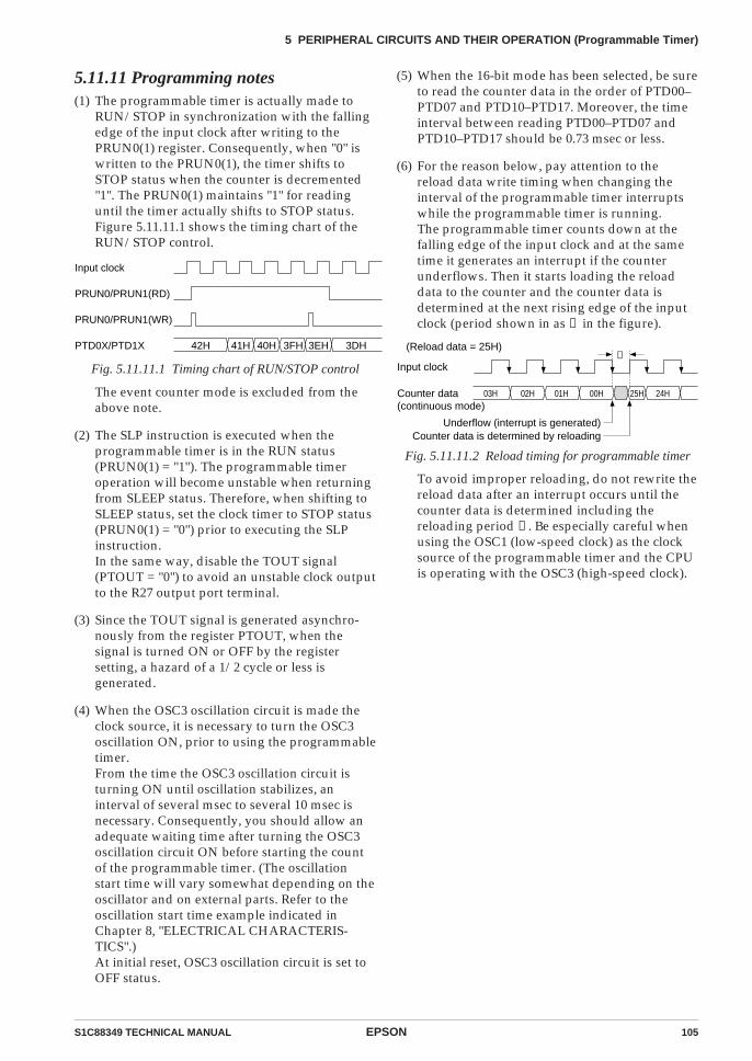
S1C88349 TECHNICAL MANUAL EPSON 105
5 PERIPHERAL CIRCUITS AND THEIR OPERATION (Programmable Timer)
5.11.11 Programming notes(1) The programmable timer is actually made to
RUN/STOP in synchronization with the fallingedge of the input clock after writing to thePRUN0(1) register. Consequently, when "0" iswritten to the PRUN0(1), the timer shifts toSTOP status when the counter is decremented"1". The PRUN0(1) maintains "1" for readinguntil the timer actually shifts to STOP status.Figure 5.11.11.1 shows the timing chart of theRUN/STOP control.
PRUN0/PRUN1(WR)
PTD0X/PTD1X 42H 41H 40H 3FH 3EH 3DH
PRUN0/PRUN1(RD)
Input clock
Fig. 5.11.11.1 Timing chart of RUN/STOP control
The event counter mode is excluded from theabove note.
(2) The SLP instruction is executed when theprogrammable timer is in the RUN status(PRUN0(1) = "1"). The programmable timeroperation will become unstable when returningfrom SLEEP status. Therefore, when shifting toSLEEP status, set the clock timer to STOP status(PRUN0(1) = "0") prior to executing the SLPinstruction.In the same way, disable the TOUT signal(PTOUT = "0") to avoid an unstable clock outputto the R27 output port terminal.
(3) Since the TOUT signal is generated asynchro-nously from the register PTOUT, when thesignal is turned ON or OFF by the registersetting, a hazard of a 1/2 cycle or less isgenerated.
(4) When the OSC3 oscillation circuit is made theclock source, it is necessary to turn the OSC3oscillation ON, prior to using the programmabletimer.From the time the OSC3 oscillation circuit isturning ON until oscillation stabilizes, aninterval of several msec to several 10 msec isnecessary. Consequently, you should allow anadequate waiting time after turning the OSC3oscillation circuit ON before starting the countof the programmable timer. (The oscillationstart time will vary somewhat depending on theoscillator and on external parts. Refer to theoscillation start time example indicated inChapter 8, "ELECTRICAL CHARACTERIS-TICS".)At initial reset, OSC3 oscillation circuit is set toOFF status.
(5) When the 16-bit mode has been selected, be sureto read the counter data in the order of PTD00–PTD07 and PTD10–PTD17. Moreover, the timeinterval between reading PTD00–PTD07 andPTD10–PTD17 should be 0.73 msec or less.
(6) For the reason below, pay attention to thereload data write timing when changing theinterval of the programmable timer interruptswhile the programmable timer is running.The programmable timer counts down at thefalling edge of the input clock and at the sametime it generates an interrupt if the counterunderflows. Then it starts loading the reloaddata to the counter and the counter data isdetermined at the next rising edge of the inputclock (period shown in as ➀ in the figure).
Input clock
Counter data (continuous mode)
(Reload data = 25H)
03H 02H 01H 00H 25H 24H
Underflow (interrupt is generated)Counter data is determined by reloading
➀
Fig. 5.11.11.2 Reload timing for programmable timer
To avoid improper reloading, do not rewrite thereload data after an interrupt occurs until thecounter data is determined including thereloading period ➀ . Be especially careful whenusing the OSC1 (low-speed clock) as the clocksource of the programmable timer and the CPUis operating with the OSC3 (high-speed clock).
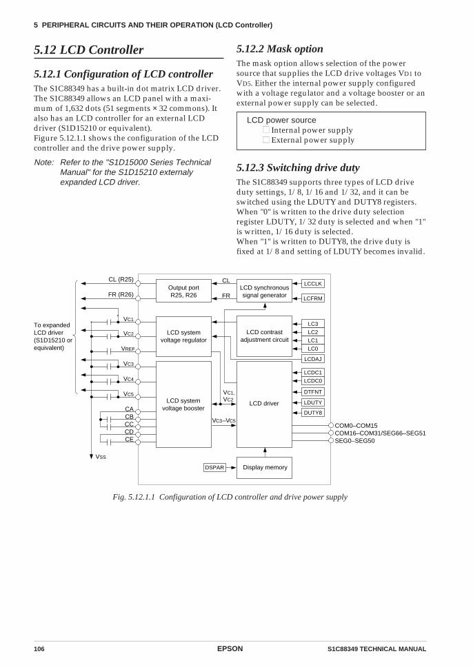
106 EPSON S1C88349 TECHNICAL MANUAL
5 PERIPHERAL CIRCUITS AND THEIR OPERATION (LCD Controller)
5.12 LCD Controller
5.12.1 Configuration of LCD controllerThe S1C88349 has a built-in dot matrix LCD driver.The S1C88349 allows an LCD panel with a maxi-mum of 1,632 dots (51 segments × 32 commons). Italso has an LCD controller for an external LCDdriver (S1D15210 or equivalent).Figure 5.12.1.1 shows the configuration of the LCDcontroller and the drive power supply.
Note: Refer to the "S1D15000 Series TechnicalManual" for the S1D15210 externalyexpanded LCD driver.
5.12.2 Mask optionThe mask option allows selection of the powersource that supplies the LCD drive voltages VD1 toVD5. Either the internal power supply configuredwith a voltage regulator and a voltage booster or anexternal power supply can be selected.
LCD power source Internal power supply External power supply
5.12.3 Switching drive dutyThe S1C88349 supports three types of LCD driveduty settings, 1/8, 1/16 and 1/32, and it can beswitched using the LDUTY and DUTY8 registers.When "0" is written to the drive duty selectionregister LDUTY, 1/32 duty is selected and when "1"is written, 1/16 duty is selected.When "1" is written to DUTY8, the drive duty isfixed at 1/8 and setting of LDUTY becomes invalid.
CL (R25)
FR (R26)
VC1
V
VREF
C2
VC3
VC4
VC5
CACBCCCDCE
LCD systemvoltage booster
VSS
LCD systemvoltage regulator
To expandedLCD driver(S1D15210 orequivalent)
Output portR25, R26
LCD synchronoussignal generator
CL
FR
LCD contrastadjustment circuit
LCCLK
LCFRM
LC3
LC2
LC1
LC0
LCDAJ
LCD driver
DTFNTVC1,
V –VC3 C5
LCDC1
LCDC0
LDUTY
DUTY8
Display memoryDSPAR
VC2
COM0–COM15COM16–COM31/SEG66–SEG51 SEG0–SEG50
Fig. 5.12.1.1 Configuration of LCD controller and drive power supply
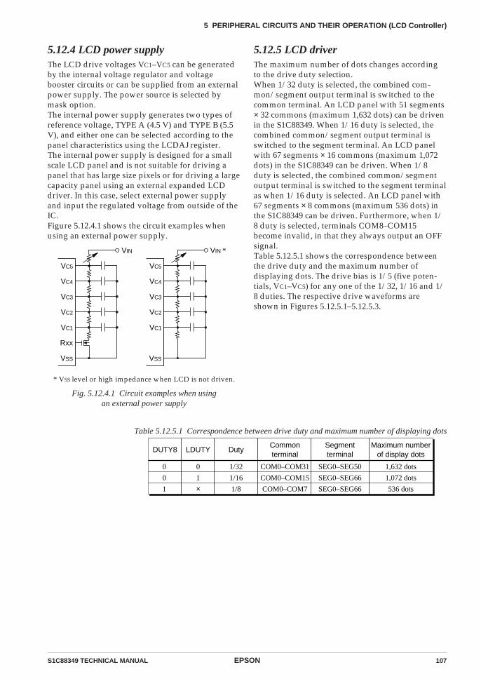
S1C88349 TECHNICAL MANUAL EPSON 107
5 PERIPHERAL CIRCUITS AND THEIR OPERATION (LCD Controller)
5.12.4 LCD power supplyThe LCD drive voltages VC1–VC5 can be generatedby the internal voltage regulator and voltagebooster circuits or can be supplied from an externalpower supply. The power source is selected bymask option.The internal power supply generates two types ofreference voltage, TYPE A (4.5 V) and TYPE B (5.5V), and either one can be selected according to thepanel characteristics using the LCDAJ register.The internal power supply is designed for a smallscale LCD panel and is not suitable for driving apanel that has large size pixels or for driving a largecapacity panel using an external expanded LCDdriver. In this case, select external power supplyand input the regulated voltage from outside of theIC.Figure 5.12.4.1 shows the circuit examples whenusing an external power supply.
DUTY8
0
0
1
LDUTY
0
1
×
Duty
1/32
1/16
1/8
Commonterminal
COM0–COM31
COM0–COM15
COM0–COM7
Segmentterminal
SEG0–SEG50
SEG0–SEG66
SEG0–SEG66
Maximum numberof display dots
1,632 dots
1,072 dots
536 dots
Table 5.12.5.1 Correspondence between drive duty and maximum number of displaying dots
VC5
VC4
VC3
VC2
VC1
Rxx
VSS
VIN
VC5
VC4
VC3
VC2
VC1
VSS
VIN *
* VSS level or high impedance when LCD is not driven.
Fig. 5.12.4.1 Circuit examples when usingan external power supply
5.12.5 LCD driverThe maximum number of dots changes accordingto the drive duty selection.When 1/32 duty is selected, the combined com-mon/segment output terminal is switched to thecommon terminal. An LCD panel with 51 segments× 32 commons (maximum 1,632 dots) can be drivenin the S1C88349. When 1/16 duty is selected, thecombined common/segment output terminal isswitched to the segment terminal. An LCD panelwith 67 segments × 16 commons (maximum 1,072dots) in the S1C88349 can be driven. When 1/8duty is selected, the combined common/segmentoutput terminal is switched to the segment terminalas when 1/16 duty is selected. An LCD panel with67 segments × 8 commons (maximum 536 dots) inthe S1C88349 can be driven. Furthermore, when 1/8 duty is selected, terminals COM8–COM15become invalid, in that they always output an OFFsignal.Table 5.12.5.1 shows the correspondence betweenthe drive duty and the maximum number ofdisplaying dots. The drive bias is 1/5 (five poten-tials, VC1–VC5) for any one of the 1/32, 1/16 and 1/8 duties. The respective drive waveforms areshown in Figures 5.12.5.1–5.12.5.3.
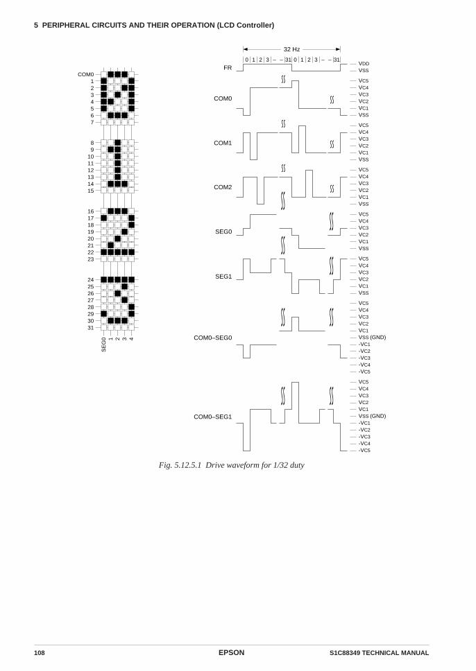
108 EPSON S1C88349 TECHNICAL MANUAL
5 PERIPHERAL CIRCUITS AND THEIR OPERATION (LCD Controller)
Fig. 5.12.5.1 Drive waveform for 1/32 duty
VDDVSS
31––321031––3210
FR
COM0
COM1
COM2
SEG0
SEG1
COM0–SEG0
COM0–SEG1
COM01234567
89
101112131415
1617181920212223
2425262728293031
SE
G0 1 2 3 4
VC5VC4VC3VC2VC1V (GND)SS
VC5VC4VC3VC2VC1V (GND)SS
~ ~
~ ~
~ ~
~ ~
~ ~
~ ~
~ ~
~ ~
~ ~
~ ~
~ ~
~ ~
~ ~
~ ~
-VC1-VC2-VC3-VC4-VC5
-VC1-VC2-VC3-VC4-VC5
VC5VC4VC3VC2VC1VSS
VC5VC4VC3VC2VC1VSS
VC5VC4VC3VC2VC1VSS
VC5VC4VC3VC2VC1VSS
VC5VC4VC3VC2VC1VSS
32 Hz
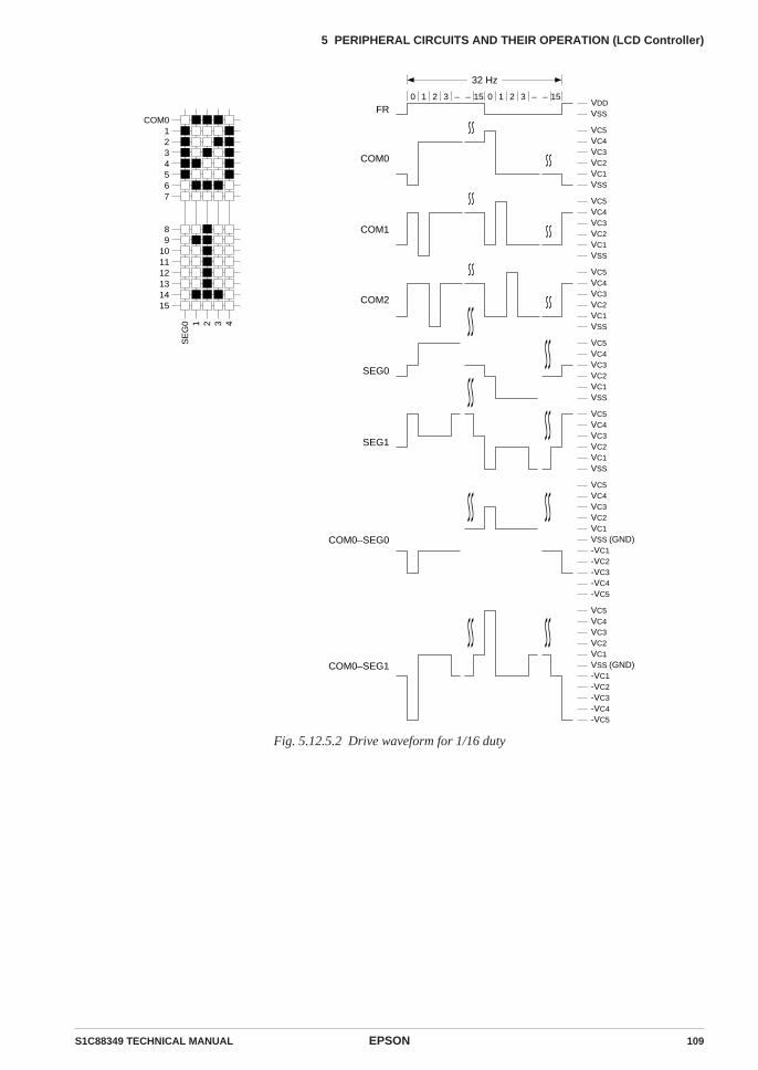
S1C88349 TECHNICAL MANUAL EPSON 109
5 PERIPHERAL CIRCUITS AND THEIR OPERATION (LCD Controller)
Fig. 5.12.5.2 Drive waveform for 1/16 duty
COM01234567
89
101112131415
SE
G0 1 2 3 4
15––321015––3210
FR
COM0
COM1
COM2
SEG0
SEG1
COM0–SEG0
COM0–SEG1
~ ~
~ ~
~ ~
~ ~
~ ~
~ ~
~ ~
~ ~
~ ~
~ ~
~ ~
~ ~
~ ~
~ ~
VDDVSS
VC5VC4VC3VC2VC1V (GND)SS
VC5VC4VC3VC2VC1V (GND)SS
-VC1-VC2-VC3-VC4-VC5
-VC1-VC2-VC3-VC4-VC5
VC5VC4VC3VC2VC1VSS
VC5VC4VC3VC2VC1VSS
VC5VC4VC3VC2VC1VSS
VC5VC4VC3VC2VC1VSS
VC5VC4VC3VC2VC1VSS
32 Hz
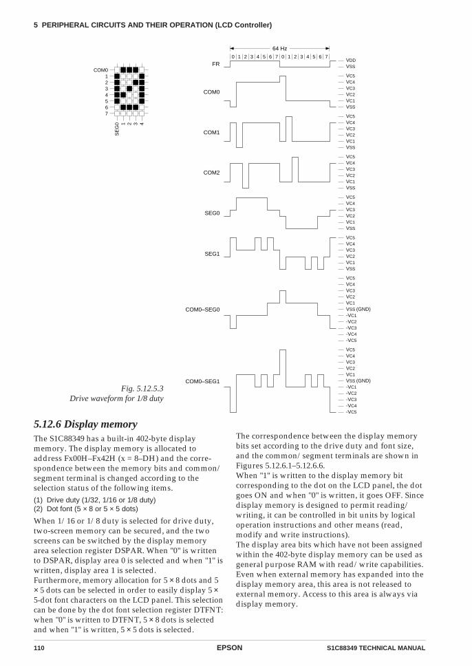
110 EPSON S1C88349 TECHNICAL MANUAL
5 PERIPHERAL CIRCUITS AND THEIR OPERATION (LCD Controller)
Fig. 5.12.5.3Drive waveform for 1/8 duty
5.12.6 Display memoryThe S1C88349 has a built-in 402-byte displaymemory. The display memory is allocated toaddress Fx00H–Fx42H (x = 8–DH) and the corre-spondence between the memory bits and common/segment terminal is changed according to theselection status of the following items.(1) Drive duty (1/32, 1/16 or 1/8 duty)(2) Dot font (5 × 8 or 5 × 5 dots)
When 1/16 or 1/8 duty is selected for drive duty,two-screen memory can be secured, and the twoscreens can be switched by the display memoryarea selection register DSPAR. When "0" is writtento DSPAR, display area 0 is selected and when "1" iswritten, display area 1 is selected.Furthermore, memory allocation for 5 × 8 dots and 5× 5 dots can be selected in order to easily display 5 ×5-dot font characters on the LCD panel. This selectioncan be done by the dot font selection register DTFNT:when "0" is written to DTFNT, 5 × 8 dots is selectedand when "1" is written, 5 × 5 dots is selected.
The correspondence between the display memorybits set according to the drive duty and font size,and the common/segment terminals are shown inFigures 5.12.6.1–5.12.6.6.When "1" is written to the display memory bitcorresponding to the dot on the LCD panel, the dotgoes ON and when "0" is written, it goes OFF. Sincedisplay memory is designed to permit reading/writing, it can be controlled in bit units by logicaloperation instructions and other means (read,modify and write instructions).The display area bits which have not been assignedwithin the 402-byte display memory can be used asgeneral purpose RAM with read/write capabilities.Even when external memory has expanded into thedisplay memory area, this area is not released toexternal memory. Access to this area is always viadisplay memory.
COM01234567
SE
G0 1 2 3 4
VDDVSS
VC5VC4VC3VC2VC1VSS
7321073210
FR
COM0
COM1
COM2
SEG0
SEG1
VC5VC4VC3VC2VC1VSS
VC5VC4VC3VC2VC1VSS
VC5VC4VC3VC2VC1VSS
VC5VC4VC3VC2VC1VSS
VC5VC4VC3VC2VC1V (GND)SS
VC5VC4VC3VC2VC1V (GND)SS
COM0–SEG0
COM0–SEG1
4 6 4 65 5
-VC1-VC2-VC3-VC4-VC5
-VC1-VC2-VC3-VC4-VC5
64 Hz
S1C88349 TECHNICAL MANUAL EPSON 111
5 PERIPHERAL CIRCUITS AND THEIR OPERATION (LCD Controller)
01
23
45
67
89
1011
1213
1415
1617
1819
2021
2223
2425
2627
2829
3031
3233
3435
3637
3839
4041
4243
4445
4647
4849
50
01
23
45
67
89
AB
CD
EF
01
23
45
67
89
AB
CD
EF
01
23
45
67
89
AB
CD
EF
01
23
45
67
89
AB
CD
EF
01
20
12
34
D0
D1
D2
D3
D4
D5
D6
D7
00F
800H
|00
F84
2H
Add
ress
/Dat
a bi
t
Dis
pla
y ar
ea
D0
D1
D2
D3
D4
D5
D6
D7
00F
900H
|00
F94
2HD
isp
lay
area
D0
D1
D2
D3
D4
D5
D6
D7
00F
A00
H|
00F
A42
H
D0
D1
D2
D3
D4
D5
D6
D7
00F
B00
H|
00F
B42
HD
isp
lay
area
D0
D1
D2
D3
D4
D5
D6
D7
00F
C00
H|
00F
C42
H
D0
D1
D2
D3
D4
D5
D6
D7
00F
D00
H|
00F
D42
H
SE
G
CO
M
0 1 2 3 4 5 6 7 8 9 10 11 12 13 14 15 16 17 18 19 20 21 22 23 24 25 26 27 28 29 30 31
Dis
pla
y ar
ea
Fig. 5.12.6.1 1/32 duty and 5 × 8 dots display memory map
112 EPSON S1C88349 TECHNICAL MANUAL
5 PERIPHERAL CIRCUITS AND THEIR OPERATION (LCD Controller)
01
23
45
67
89
1011
1213
1415
1617
1819
2021
2223
2425
2627
2829
3031
3233
3435
3637
3839
4041
4243
4445
4647
4849
50
01
23
45
67
89
AB
CD
EF
01
23
45
67
89
AB
CD
EF
01
23
45
67
89
AB
CD
EF
01
23
45
67
89
AB
CD
EF
01
20
12
34
D0
D1
D2
D3
D4
D5
D6
D7
00F
800H
|00
F84
2H
Add
ress
/Dat
a bi
t
Dis
pla
y ar
ea
D0
D1
D2
D3
D4
D5
D6
D7
00F
900H
|00
F94
2H
Dis
pla
y ar
ea
D0
D1
D2
D3
D4
D5
D6
D7
00F
A00
H|
00F
A42
H
D0
D1
D2
D3
D4
D5
D6
D7
00F
B00
H|
00F
B42
H
Dis
pla
y ar
ea
D0
D1
D2
D3
D4
D5
D6
D7
00F
C00
H|
00F
C42
H
D0
D1
D2
D3
D4
D5
D6
D7
00F
D00
H|
00F
D42
H
SE
G
CO
M
0 1 2 3 4 5 6 7 8 9 10 11 12 13 14 15 16 17 18 19 20 21 22 23 24 25 26 27 28 29 30 31
Dis
pla
y ar
ea
Dis
pla
y ar
ea
Dis
pla
y ar
ea
Fig. 5.12.6.2 1/32 duty and 5 × 5 dots display memory map
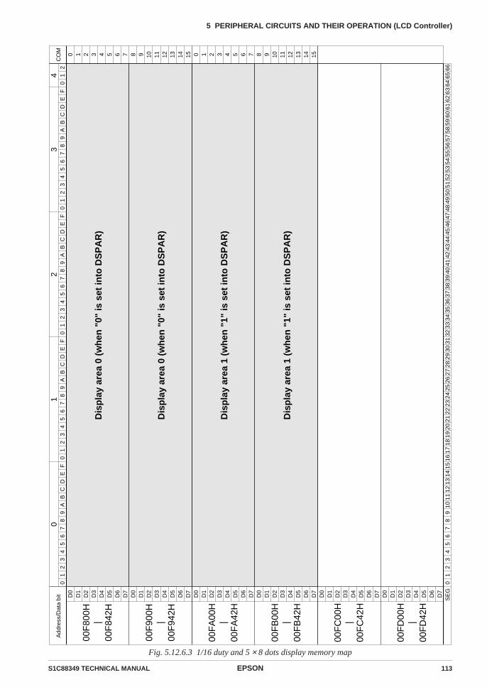
S1C88349 TECHNICAL MANUAL EPSON 113
5 PERIPHERAL CIRCUITS AND THEIR OPERATION (LCD Controller)
01
23
45
67
89
1011
1213
1415
1617
1819
2021
2223
2425
2627
2829
3031
3233
3435
3637
3839
4041
4243
4445
4647
4849
5051
5253
5455
5657
5859
6061
6263
6465
66
01
23
45
67
89
AB
CD
EF
01
23
45
67
89
AB
CD
EF
01
23
45
67
89
AB
CD
EF
01
23
45
67
89
AB
CD
EF
01
20
12
34
D0
D1
D2
D3
D4
D5
D6
D7
00F
800H
|00
F84
2H
Add
ress
/Dat
a bi
t
Dis
pla
y ar
ea 0
(w
hen
"0"
is s
et in
to D
SP
AR
)
D0
D1
D2
D3
D4
D5
D6
D7
00F
900H
|00
F94
2HD
isp
lay
area
0 (
wh
en "
0" is
set
into
DS
PA
R)
D0
D1
D2
D3
D4
D5
D6
D7
00F
A00
H|
00F
A42
H
D0
D1
D2
D3
D4
D5
D6
D7
00F
B00
H|
00F
B42
HD
isp
lay
area
1 (
wh
en "
1" is
set
into
DS
PA
R)
D0
D1
D2
D3
D4
D5
D6
D7
00F
C00
H|
00F
C42
H
D0
D1
D2
D3
D4
D5
D6
D7
00F
D00
H|
00F
D42
H
SE
G
CO
M
0 1 2 3 4 5 6 7 8 9 10 11 12 13 14 15 0 1 2 3 4 5 6 7 8 9 10 11 12 13 14 15
Dis
pla
y ar
ea 1
(w
hen
"1"
is s
et in
to D
SP
AR
)
Fig. 5.12.6.3 1/16 duty and 5 × 8 dots display memory map
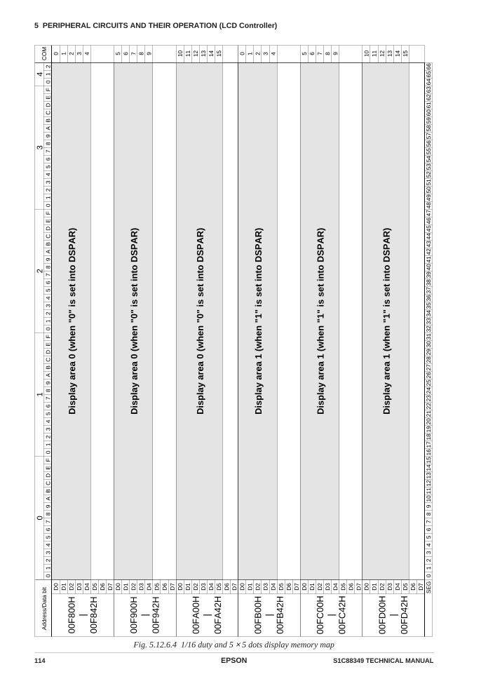
114 EPSON S1C88349 TECHNICAL MANUAL
5 PERIPHERAL CIRCUITS AND THEIR OPERATION (LCD Controller)
01
23
45
67
89
1011
1213
1415
1617
1819
2021
2223
2425
2627
2829
3031
3233
3435
3637
3839
4041
4243
4445
4647
4849
5051
5253
5455
5657
5859
6061
6263
6465
66
01
23
45
67
89
AB
CD
EF
01
23
45
67
89
AB
CD
EF
01
23
45
67
89
AB
CD
EF
01
23
45
67
89
AB
CD
EF
01
20
12
34
D0
D1
D2
D3
D4
D5
D6
D7
00F
800H
|00
F84
2H
Add
ress
/Dat
a bi
t
Dis
pla
y ar
ea 0
(w
hen
"0"
is s
et in
to D
SP
AR
)
D0
D1
D2
D3
D4
D5
D6
D7
00F
900H
|00
F94
2H
Dis
pla
y ar
ea 0
(w
hen
"0"
is s
et in
to D
SP
AR
)
D0
D1
D2
D3
D4
D5
D6
D7
00F
A00
H|
00F
A42
H
D0
D1
D2
D3
D4
D5
D6
D7
00F
B00
H|
00F
B42
H
Dis
pla
y ar
ea 1
(w
hen
"1"
is s
et in
to D
SP
AR
)
D0
D1
D2
D3
D4
D5
D6
D7
00F
C00
H|
00F
C42
H
Dis
pla
y ar
ea 1
(w
hen
"1"
is s
et in
to D
SP
AR
)
D0
D1
D2
D3
D4
D5
D6
D7
00F
D00
H|
00F
D42
H
SE
G
CO
M
0 1 2 3 4 5 6 7 8 9 10 11 12 13 14 15 0 1 2 3 4 5 6 7 8 9 10 11 12 13 14 15
Dis
pla
y ar
ea 0
(w
hen
"0"
is s
et in
to D
SP
AR
)
Dis
pla
y ar
ea 1
(w
hen
"1"
is s
et in
to D
SP
AR
)
Fig. 5.12.6.4 1/16 duty and 5 × 5 dots display memory map
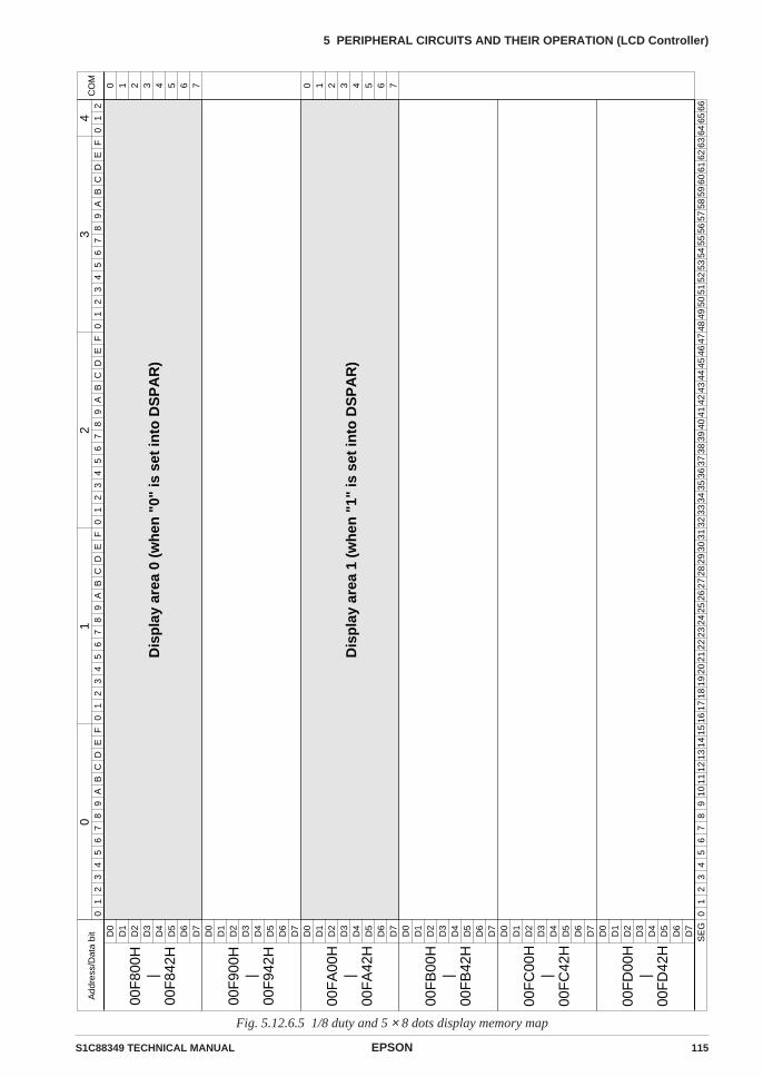
S1C88349 TECHNICAL MANUAL EPSON 115
5 PERIPHERAL CIRCUITS AND THEIR OPERATION (LCD Controller)
01
23
45
67
89
1011
1213
1415
1617
1819
2021
2223
2425
2627
2829
3031
3233
3435
3637
3839
4041
4243
4445
4647
4849
5051
5253
5455
5657
5859
6061
6263
6465
66
01
23
45
67
89
AB
CD
EF
01
23
45
67
89
AB
CD
EF
01
23
45
67
89
AB
CD
EF
01
23
45
67
89
AB
CD
EF
01
20
12
34
D0
D1
D2
D3
D4
D5
D6
D7
00F
800H
|00
F84
2H
Add
ress
/Dat
a bi
t
Dis
pla
y ar
ea 0
(w
hen
"0"
is s
et in
to D
SP
AR
)
D0
D1
D2
D3
D4
D5
D6
D7
00F
900H
|00
F94
2H
D0
D1
D2
D3
D4
D5
D6
D7
00F
A00
H|
00F
A42
H
D0
D1
D2
D3
D4
D5
D6
D7
00F
B00
H|
00F
B42
H
D0
D1
D2
D3
D4
D5
D6
D7
00F
C00
H|
00F
C42
H
D0
D1
D2
D3
D4
D5
D6
D7
00F
D00
H|
00F
D42
H
SE
G
CO
M
0 1 2 3 4 5 6 7 0 1 2 3 4 5 6 7
Dis
pla
y ar
ea 1
(w
hen
"1"
is s
et in
to D
SP
AR
)
Fig. 5.12.6.5 1/8 duty and 5 × 8 dots display memory map
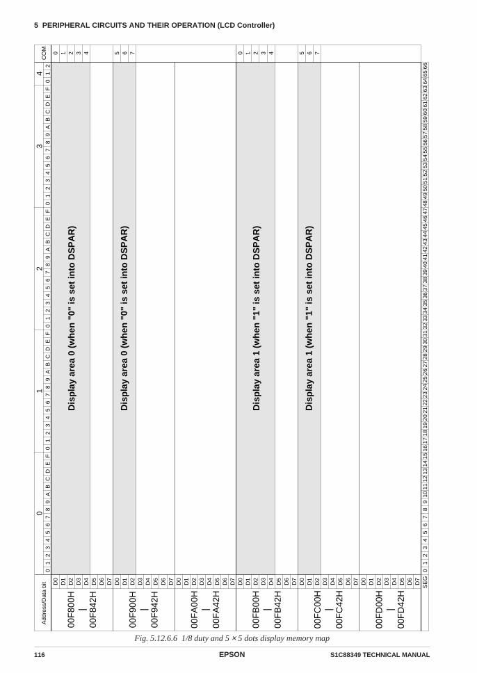
116 EPSON S1C88349 TECHNICAL MANUAL
5 PERIPHERAL CIRCUITS AND THEIR OPERATION (LCD Controller)
01
23
45
67
89
1011
1213
1415
1617
1819
2021
2223
2425
2627
2829
3031
3233
3435
3637
3839
4041
4243
4445
4647
4849
5051
5253
5455
5657
5859
6061
6263
6465
66
01
23
45
67
89
AB
CD
EF
01
23
45
67
89
AB
CD
EF
01
23
45
67
89
AB
CD
EF
01
23
45
67
89
AB
CD
EF
01
20
12
34
D0
D1
D2
D3
D4
D5
D6
D7
00F
800H
|00
F84
2H
Add
ress
/Dat
a bi
t
Dis
pla
y ar
ea 0
(w
hen
"0"
is s
et in
to D
SP
AR
)
D0
D1
D2
D3
D4
D5
D6
D7
00F
900H
|00
F94
2H
Dis
pla
y ar
ea 0
(w
hen
"0"
is s
et in
to D
SP
AR
)
D0
D1
D2
D3
D4
D5
D6
D7
00F
A00
H|
00F
A42
H
D0
D1
D2
D3
D4
D5
D6
D7
00F
B00
H|
00F
B42
H
Dis
pla
y ar
ea 1
(w
hen
"1"
is s
et in
to D
SP
AR
)
D0
D1
D2
D3
D4
D5
D6
D7
00F
C00
H|
00F
C42
H
Dis
pla
y ar
ea 1
(w
hen
"1"
is s
et in
to D
SP
AR
)
D0
D1
D2
D3
D4
D5
D6
D7
00F
D00
H|
00F
D42
H
SE
G
CO
M
0 1 2 3 4 5 6 7 0 1 2 3 4 5 6 7
Fig. 5.12.6.6 1/8 duty and 5 × 5 dots display memory map
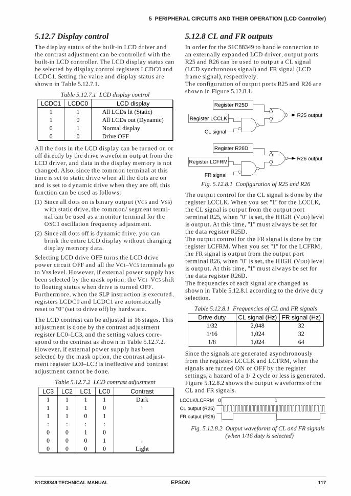
S1C88349 TECHNICAL MANUAL EPSON 117
5 PERIPHERAL CIRCUITS AND THEIR OPERATION (LCD Controller)
5.12.7 Display controlThe display status of the built-in LCD driver andthe contrast adjustment can be controlled with thebuilt-in LCD controller. The LCD display status canbe selected by display control registers LCDC0 andLCDC1. Setting the value and display status areshown in Table 5.12.7.1.
Table 5.12.7.1 LCD display control
5.12.8 CL and FR outputsIn order for the S1C88349 to handle connection toan externally expanded LCD driver, output portsR25 and R26 can be used to output a CL signal(LCD synchronous signal) and FR signal (LCDframe signal), respectively.The configuration of output ports R25 and R26 areshown in Figure 5.12.8.1.
LCDC1 LCDC0 LCD display1100
1010
All LCDs lit (Static)All LCDs out (Dynamic)Normal displayDrive OFF
All the dots in the LCD display can be turned on oroff directly by the drive waveform output from theLCD driver, and data in the display memory is notchanged. Also, since the common terminal at thistime is set to static drive when all the dots are onand is set to dynamic drive when they are off, thisfunction can be used as follows:
(1) Since all dots on is binary output (VC5 and VSS)with static drive, the common/segment termi-nal can be used as a monitor terminal for theOSC1 oscillation frequency adjustment.
(2) Since all dots off is dynamic drive, you canbrink the entire LCD display without changingdisplay memory data.
Selecting LCD drive OFF turns the LCD drivepower circuit OFF and all the VC1–VC5 terminals goto VSS level. However, if external power supply hasbeen selected by the mask option, the VC1–VC5 shiftto floating status when drive is turned OFF.Furthermore, when the SLP instruction is executed,registers LCDC0 and LCDC1 are automaticallyreset to "0" (set to drive off) by hardware.
The LCD contrast can be adjusted in 16 stages. Thisadjustment is done by the contrast adjustmentregister LC0–LC3, and the setting values corre-spond to the contrast as shown in Table 5.12.7.2.However, if external power supply has beenselected by the mask option, the contrast adjust-ment register LC0–LC3 is ineffective and contrastadjustment cannot be done.
Table 5.12.7.2 LCD contrast adjustment
LC3 LC0 Contrast111:000
101:010
Dark
Light
LC1110:100
LC2111:000
↑
↓
Register R25D
Register LCCLKR25 output
CL signal
Register R26D
Register LCFRMR26 output
FR signal
Fig. 5.12.8.1 Configuration of R25 and R26
The output control for the CL signal is done by theregister LCCLK. When you set "1" for the LCCLK,the CL signal is output from the output portterminal R25, when "0" is set, the HIGH (VDD) levelis output. At this time, "1" must always be set forthe data register R25D.The output control for the FR signal is done by theregister LCFRM. When you set "1" for the LCFRM,the FR signal is output from the output portterminal R26, when "0" is set, the HIGH (VDD) levelis output. At this time, "1" must always be set forthe data register R26D.The frequencies of each signal are changed asshown in Table 5.12.8.1 according to the drive dutyselection.
Table 5.12.8.1 Frequencies of CL and FR signals
Drive duty1/321/161/8
CL signal (Hz)2,0481,0241,024
FR signal (Hz)323264
Since the signals are generated asynchronouslyfrom the registers LCCLK and LCFRM, when thesignals are turned ON or OFF by the registersettings, a hazard of a 1/2 cycle or less is generated.Figure 5.12.8.2 shows the output waveforms of theCL and FR signals.
Fig. 5.12.8.2 Output waveforms of CL and FR signals (when 1/16 duty is selected)
LCCLK/LCFRM
CL output (R25)
FR output (R26)
0 1
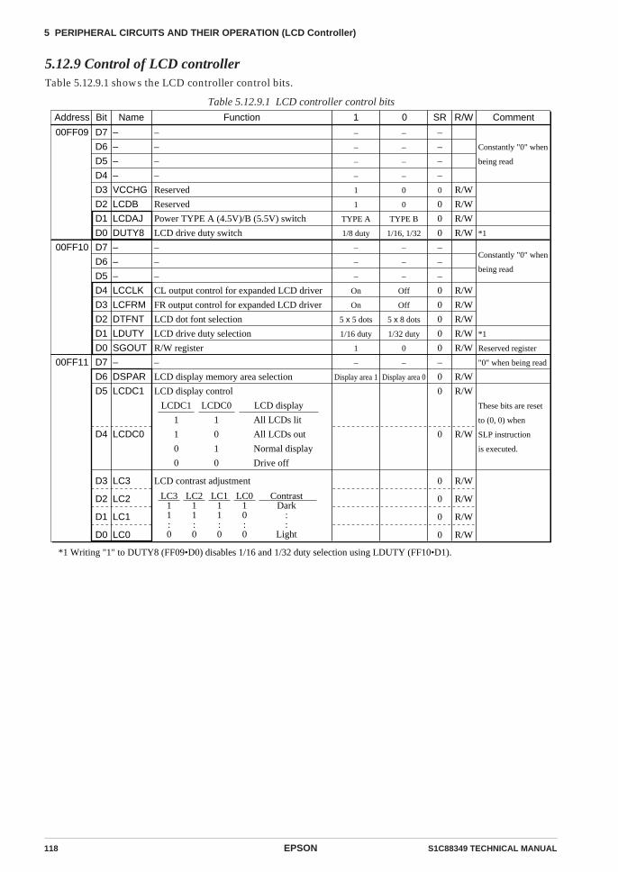
118 EPSON S1C88349 TECHNICAL MANUAL
5 PERIPHERAL CIRCUITS AND THEIR OPERATION (LCD Controller)
5.12.9 Control of LCD controllerTable 5.12.9.1 shows the LCD controller control bits.
Table 5.12.9.1 LCD controller control bits
Address Bit Name
00FF10 D7
D6
D5
D4
D3
D2
D1
D0
–
–
–
LCCLK
LCFRM
DTFNT
LDUTY
SGOUT
SR R/WFunction Comment
–
–
–
CL output control for expanded LCD driver
FR output control for expanded LCD driver
LCD dot font selection
LCD drive duty selection
R/W register
Constantly "0" when
being read
1 0
–
–
–
0
0
0
0
0
R/W
R/W
R/W
R/W
R/W
–
–
–
On
On
5 x 5 dots
1/16 duty
1
–
–
–
Off
Off
5 x 8 dots
1/32 duty
0
00FF11 D7
D6
D5
D4
D3
D2
D1
D0
–
DSPAR
LCDC1
LCDC0
LC3
LC2
LC1
LC0
–
LCD display memory area selection
LCD display control
LCD contrast adjustment
"0" when being read
These bits are reset
to (0, 0) when
SLP instruction
is executed.
–
0
0
0
0
0
0
0
R/W
R/W
R/W
R/W
R/W
R/W
R/W
–
Display area 1
–
Display area 0
LCDC1
1
1
0
0
LCDC0
1
0
1
0
LCD display
All LCDs lit
All LCDs out
Normal display
Drive off
LC311:0
LC211:0
LC111:0
LC010:0
ContrastDark
::
Light
*1
Reserved register
00FF09 D7
D6
D5
D4
D3
D2
D1
D0
–
–
–
–
VCCHG
LCDB
LCDAJ
DUTY8
–
–
–
–
Reserved
Reserved
Power TYPE A (4.5V)/B (5.5V) switch
LCD drive duty switch
Constantly "0" when
being read
–
–
–
–
0
0
0
0
R/W
R/W
R/W
R/W
–
–
–
–
1
1
TYPE A
1/8 duty
–
–
–
–
0
0
TYPE B
1/16, 1/32 *1
*1 Writing "1" to DUTY8 (FF09•D0) disables 1/16 and 1/32 duty selection using LDUTY (FF10•D1).
S1C88349 TECHNICAL MANUAL EPSON 119
5 PERIPHERAL CIRCUITS AND THEIR OPERATION (LCD Controller)
LCDAJ: 00FF09H•D1Switches the internal power supply.
When "1" is written: TYPE AWhen "0" is written: TYPE BReading: Valid
LCDAJ is the LCD power switching register. When"1" is written, the LCD power supply is set forTYPE A (4.5 V) and when "0" is written the LCDpower supply is set for TYPE B (5.5 V).At initial reset, LCDAJ is set to "0" (TYPE B).
DUTY8: 00FF09H•D0Switches the drive duty.
When "1" is written: 1/8 dutyWhen "0" is written: 1/16 or 1/32 dutyReading: Valid
DUTY8 is the drive duty switching register. When"1" is written, 1/8 duty is selected and when "0" iswritten, 1/16 or 1/32 duty is selected.When "1" is written to DUTY8, switching between1/16 duty and 1/32 duty using LDUTY becomesinvalid.At initial reset, DUTY8 is set to "0" (1/16 or 1/32duty).
LDUTY: 00FF10H•D1Selects the drive duty.
When "1" is written: 1/16 dutyWhen "0" is written: 1/32 dutyReading: Valid
When "0" is written to LDUTY, 1/32 duty isselected and the combined common/segmentoutput terminal is switched to the common termi-nal.When "1" is written to LDUTY, 1/16 duty is selectedand the combined common/segment outputterminal is switched to the segment terminal.When "1" is written to DUTY8, the combinedcommon/segment terminals are fixed to thesegment terminals and the setting of LDUTYbecomes invalid.The correspondence between the display memorybits set according to the drive duty, and the com-mon/segment terminals are shown in Figures5.12.6.1–5.12.6.6.At initial reset, LDUTY is set to "0" (1/32 duty).
DTFNT: 00FF10H•D2Selects the dot font.
When "1" is written: 5 × 5 dotsWhen "0" is written: 5 × 8 dotsReading: Valid
Select 5 × 8 dots or 5 × 5 dots type for the displaymemory area.When "0" is written to DTFNT, 5 × 8 dots is selectedand when "1" is written, 5 × 5 dots is selected.The correspondence between the display memorybits set according to the dot font, and the common/segment terminals are shown in Figures 5.12.6.1–5.12.6.6.At initial reset, DTFNT is set to "0" (5 × 8 dots).
DSPAR: 00FF11H•D6Selects the display area.
When "1" is written: Display area 1When "0" is written: Display area 0Reading: Valid
Selects which display area is secured for twoscreens in the display memory, will be displayedwhen 1/16 or 1/8 duty is selected.When "0" is written to DSPAR, display area 0 isselected and when "1" is written, display area 1 isselected.When 1/32 duty is selected, since the display areais only for one screen, the setting of DSPARbecomes invalid.The correspondence between the display memorybits set according to the display area, and thecommon/segment terminals are shown in Figures5.12.6.1–5.12.6.6.At initial reset, DSPAR is set to "0" (display area 0).
LCDC0, LCDC1: 00FF11H•D4, D5Controls the LCD display.
Table 5.12.9.2 LCD display control
LCDC1 LCDC0 LCD display1100
1010
All LCDs lit (Static)All LCDs out (Dynamic)Normal displayDrive OFF
The four settings mentioned above can be madewithout changing the display memory data.At initial reset and in the SLEEP status, this registeris set to "0" (drive off).
120 EPSON S1C88349 TECHNICAL MANUAL
5 PERIPHERAL CIRCUITS AND THEIR OPERATION (LCD Controller)
LC0–LC3: 00FF11H•D0–D3Adjusts the LCD contrast.
Table 5.12.9.3 LCD contract adjustment
LC3 LC0 Contrast
1
1
1
1
1
1
1
1
0
0
0
0
0
0
0
0
1
0
1
0
1
0
1
0
1
0
1
0
1
0
1
0
Dark
↑
↓Light
LC1
1
1
0
0
1
1
0
0
1
1
0
0
1
1
0
0
LC2
1
1
1
1
0
0
0
0
1
1
1
1
0
0
0
0
The contrast can be adjusted in 16 stages as men-tioned above. This adjustment changes the drivevoltage on terminals VC1–VC5.At initial reset, this register is set to "0".
LCCLK: 00FF10H•D4Controls the CL signal output.
When "1" is written: CL signal outputWhen "0" is written: HIGH level (DC) outputReading: Valid
LCCLK is the output control register for CL signal.When "1" is set, the CL signal is output from theoutput port terminal R25 and when "0" is set, HIGH(VDD) level is output. At this time, "1" must alwaysbe set for the data register R25D.At initial reset, LCCLK is set to "0" (HIGH leveloutput).
LCFRM: 00FF10H•D3Controls the FR signal output.
When "1" is written: FR signal outputWhen "0" is written: HIGH level (DC) outputReading: Valid
LCFRM is the output control register for FR signal.When "1" is set, the FR signal is output from theoutput port terminal R26 and when "0" is set, HIGH(VDD) level is output. At this time, "1" must alwaysbe set for the data register R26D.At initial reset, LCFRM is set to "0" (HIGH leveloutput).
5.12.10 Programming notes(1) Since the CL and FR signals are generated
asynchronously from the output controlregisters LCCLK and LCFRM, when the signalsis turned ON or OFF by setting of the registersLCCLK and LCFRM, a hazard of a 1/2 cycle orless is generated.
(2) When the SLP instruction is executed, displaycontrol registers LCDC0 and LCDC1 areautomatically reset to "0" by hardware.Furthermore, in the SLEEP status, HIGH (VDD)level is output for the CL and FR signals. (Whenregisters R25D and R26D are set to "1".)
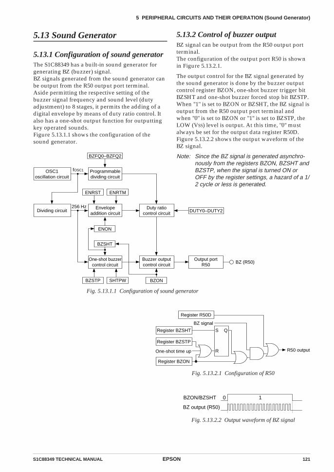
S1C88349 TECHNICAL MANUAL EPSON 121
5 PERIPHERAL CIRCUITS AND THEIR OPERATION (Sound Generator)
5.13 Sound Generator
5.13.1 Configuration of sound generatorThe S1C88349 has a built-in sound generator forgenerating BZ (buzzer) signal.BZ signals generated from the sound generator canbe output from the R50 output port terminal.Aside permitting the respective setting of thebuzzer signal frequency and sound level (dutyadjustment) to 8 stages, it permits the adding of adigital envelope by means of duty ratio control. Italso has a one-shot output function for outputtingkey operated sounds.Figure 5.13.1.1 shows the configuration of thesound generator.
5.13.2 Control of buzzer outputBZ signal can be output from the R50 output portterminal.The configuration of the output port R50 is shownin Figure 5.13.2.1.
The output control for the BZ signal generated bythe sound generator is done by the buzzer outputcontrol register BZON, one-shot buzzer trigger bitBZSHT and one-shot buzzer forced stop bit BZSTP.When "1" is set to BZON or BZSHT, the BZ signal isoutput from the R50 output port terminal andwhen "0" is set to BZON or "1" is set to BZSTP, theLOW (VSS) level is output. At this time, "0" mustalways be set for the output data register R50D.Figure 5.13.2.2 shows the output waveform of theBZ signal.
Note: Since the BZ signal is generated asynchro-nously from the registers BZON, BZSHT andBZSTP, when the signal is turned ON orOFF by the register settings, a hazard of a 1/2 cycle or less is generated.
Fig. 5.13.1.1 Configuration of sound generator
Register BZSTP
Register BZON
Register BZSHT
R
S Q
One-shot time up R50 output
BZ signal
Register R50D
Fig. 5.13.2.1 Configuration of R50
Fig. 5.13.2.2 Output waveform of BZ signal
BZON/BZSHT
BZ output (R50)
0 1
Dividing circuit256 Hz Envelope
addition circuit
Programmabledividing circuit
BZFQ0–BZFQ2
DUTY0–DUTY2Duty ratio
control circuit
ENRTM
BZON
ENON
ENRST
OSC1oscillation circuit
fOSC1
BZSHT
One-shot buzzercontrol circuit
SHTPWBZSTP
Buzzer outputcontrol circuit
Output portR50 BZ (R50)
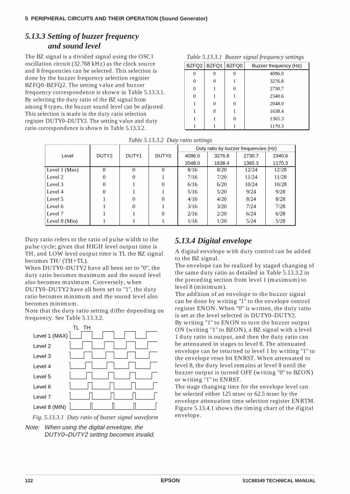
122 EPSON S1C88349 TECHNICAL MANUAL
5 PERIPHERAL CIRCUITS AND THEIR OPERATION (Sound Generator)
Table 5.13.3.2 Duty ratio settings
By selecting the duty ratio of the BZ signal fromamong 8 types, the buzzer sound level can be adjusted.This selection is made in the duty ratio selectionregister DUTY0–DUTY2. The setting value and dutyratio correspondence is shown in Table 5.13.3.2.
5.13.3 Setting of buzzer frequencyand sound level
The BZ signal is a divided signal using the OSC1oscillation circuit (32.768 kHz) as the clock sourceand 8 frequencies can be selected. This selection isdone by the buzzer frequency selection registerBZFQ0–BZFQ2. The setting value and buzzerfrequency correspondence is shown in Table 5.13.3.1.
Table 5.13.3.1 Buzzer signal frequency settings
BZFQ2 Buzzer frequency (Hz)
0
0
0
0
1
1
1
1
4096.0
3276.8
2730.7
2340.6
2048.0
1638.4
1365.3
1170.3
BZFQ1
0
0
1
1
0
0
1
1
BZFQ0
0
1
0
1
0
1
0
1
5.13.4 Digital envelopeA digital envelope with duty control can be addedto the BZ signal.The envelope can be realized by staged changing ofthe same duty ratio as detailed in Table 5.13.3.2 inthe preceding section from level 1 (maximum) tolevel 8 (minimum).The addition of an envelope to the buzzer signalcan be done by writing "1" to the envelope controlregister ENON. When "0" is written, the duty ratiois set at the level selected in DUTY0–DUTY2.By writing "1" to ENON to turn the buzzer outputON (writing "1" to BZON), a BZ signal with a level1 duty ratio is output, and then the duty ratio canbe attenuated in stages to level 8. The attenuatedenvelope can be returned to level 1 by writing "1" tothe envelope reset bit ENRST. When attenuated tolevel 8, the duty level remains at level 8 until thebuzzer output is turned OFF (writing "0" to BZON)or writing "1" to ENRST.The stage changing time for the envelope level canbe selected either 125 msec or 62.5 msec by theenvelope attenuation time selection register ENRTM.Figure 5.13.4.1 shows the timing chart of the digitalenvelope.
Duty ratio refers to the ratio of pulse width to thepulse cycle; given that HIGH level output time isTH, and LOW level output time is TL the BZ signalbecomes TH/(TH+TL).When DUTY0–DUTY2 have all been set to "0", theduty ratio becomes maximum and the sound levelalso becomes maximum. Conversely, whenDUTY0–DUTY2 have all been set to "1", the dutyratio becomes minimum and the sound level alsobecomes minimum.Note that the duty ratio setting differ depending onfrequency. See Table 5.13.3.2.
Level 1 (MAX)
Level 2
Level 3
Level 4
Level 5
Level 6
Level 7
Level 8 (MIN)
TL TH
Fig. 5.13.3.1 Duty ratio of buzzer signal waveform
Note: When using the digital envelope, theDUTY0–DUTY2 setting becomes invalid.
Level
Level 1 (Max)Level 2Level 3Level 4Level 5Level 6Level 7Level 8 (Min)
12/2811/2810/289/288/287/286/285/28
4096.0
2048.0
3276.8
1638.4
2730.7
1365.3
2340.6
1170.3
DUTY0DUTY2 DUTY1
8/207/206/205/204/203/202/201/20
01010101
00001111
8/167/166/165/164/163/162/161/16
12/2411/2410/249/248/247/246/245/24
00110011
Duty ratio by buzzer frequencies (Hz)

S1C88349 TECHNICAL MANUAL EPSON 123
5 PERIPHERAL CIRCUITS AND THEIR OPERATION (Sound Generator)
BZFQ0–2
ENON
ENRST
ENRTM
BZON
t01t02
t03t04
t05t06
t07
t01t11
t12t13
t14t15
t16t17
level 1 (MAX)2345678 (MIN)
BZ signalduty ratio
No change of duty level
t01
t02–07
= 62.5 msec= 62.5 msec
+0–4 t11
t12–17
= 125 msec= 125 msec
+0–4
5.13.5 One-shot outputThe sound generator has a built-in one-shot outputfunction for outputting a short duration buzzersignal for key operation sounds and similar effects.Either 125 msec or 31.25 msec can be selected by theone-shot buzzer duration selection register SHTPWfor buzzer signal output time.The output control of the one-shot buzzer is doneby writing "1" to the one-shot buzzer triggerBZSHT, then the BZ signal is output in synchroni-zation with the internal 256 Hz signal from the R50output port terminal. Thereafter, when the set timehas elapsed, the BZ signal in synchronization withthe 256 Hz signal automatically goes OFF in thesame manner.The BZSHT can be read to determine status. WhenBZSHT is "1", it indicates a BUSY status (duringone-shot output) and when BZSHT is "0", it indi-cates a READY status (during stop).When you want to turn the BZ signal OFF prior tothe elapse of the set time, the BZ signal can beimmediately stopped (goes OFF in asynchronizationwith 256 Hz signal) by writing "1" to the one-shotforced stop bit BZSTP.
Since the one-shot output has a short duration, anenvelope cannot be added. (When "1" is written toBZSHT, ENON is automatically reset to "0".)Consequently, only the frequency and sound levelcan be set for one-shot output.
The control for the one-shot output is invalidduring normal buzzer output.
Figure 5.13.5.1 shows the timing chart of the one-shot output.
Fig. 5.13.4.1 Timing chart of digital envelope
256 Hz
SHTPW
BZSHT(W)
BZSHT(R)
BZSTP
BZ output (R50)
Fig. 5.13.5.1 Timing chart of one-shot output

124 EPSON S1C88349 TECHNICAL MANUAL
5 PERIPHERAL CIRCUITS AND THEIR OPERATION (Sound Generator)
5.13.6 Control of sound generatorTable 5.13.6.1 shows the sound generator control bits.
Table 5.13.6.1 Sound generator control bits
BZON: 00FF44H•D0Controls the BZ signal output.
When "1" is written: BZ signal outputWhen "0" is written: LOW level (DC) outputReading: Valid
BZON is the output control register for BZ signal.When "1" is set, the BZ signal is output from theoutput port terminal R50 and when "0" is set, LOW(VSS) level is output. At this time, "0" must alwaysbe set for the data register R50D.At initial reset, BZON is set to "0" (LOW leveloutput).
BZFQ0–BZFQ2: 00FF45H•D0–D2Selects the BZ signal frequency.
Table 5.13.6.2 Buzzer frequency settings
BZFQ2 Buzzer frequency (Hz)
0
0
0
0
1
1
1
1
4096.0
3276.8
2730.7
2340.6
2048.0
1638.4
1365.3
1170.3
BZFQ1
0
0
1
1
0
0
1
1
BZFQ0
0
1
0
1
0
1
0
1
The buzzer frequency can be selected from amongthe above 8 types that have divided the OSC1 clock.At initial reset, this register is set at "0" (4096.0 Hz).
Address Bit Name SR R/WFunction Comment1 0
00FF44 D7
D6
D5
D4
D3
D2
D1
D0
–
BZSTP
BZSHT
SHTPW
ENRTM
ENRST
ENON
BZON
–
One-shot buzzer forcibly stop
One-shot buzzer trigger/status
One-shot buzzer duration width selection
Envelope attenuation time
Envelope reset
Envelope On/Off control
Buzzer output control
Constantly "0" when
being read
"0" when being read
*1
–
–
0
0
0
–
0
0
W
R/W
R/W
R/W
W
R/W
R/W
–
Forcibly stop
Busy
Trigger
125 msec
1 sec
Reset
On
On
–
No operation
Ready
No operation
31.25 msec
0.5 sec
No operation
Off
Off
00FF45 D7
D6
D5
D4
D3
D2
D1
D0
–
DUTY2
DUTY1
DUTY0
–
BZFQ2
BZFQ1
BZFQ0
–
Buzzer signal duty ratio selection
–
Buzzer frequency selection
"0" when being read
"0" when being read
–
0
0
0
–
0
0
0
R/W
R/W
R/W
R/W
R/W
R/W
–
–
–
–
00001111
R
W
00110011
01010101
8/167/166/165/164/163/162/161/16
4096.02048.0
8/207/206/205/204/203/202/201/20
3276.81638.4
12/2411/2410/249/248/247/246/245/24
2730.71365.3
12/2811/2810/289/288/287/286/285/28
2340.61170.3
2 1 0
Buzzer frequency (Hz)DUTY2–1
BZFQ2
00001111
BZFQ1
00110011
BZFQ0
01010101
Frequency (Hz)
4096.03276.82730.72340.62048.01638.41365.31170.3
*1 Reset to "0" during one-shot output.
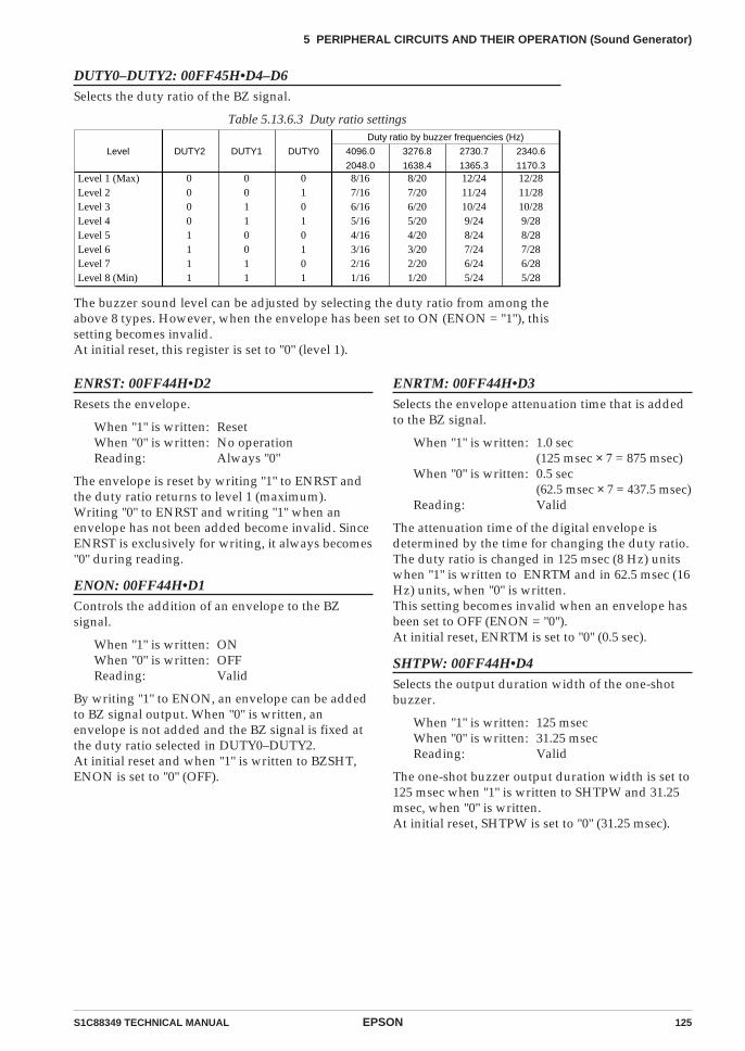
S1C88349 TECHNICAL MANUAL EPSON 125
5 PERIPHERAL CIRCUITS AND THEIR OPERATION (Sound Generator)
DUTY0–DUTY2: 00FF45H•D4–D6Selects the duty ratio of the BZ signal.
Table 5.13.6.3 Duty ratio settings
ENRST: 00FF44H•D2Resets the envelope.
When "1" is written: ResetWhen "0" is written: No operationReading: Always "0"
The envelope is reset by writing "1" to ENRST andthe duty ratio returns to level 1 (maximum).Writing "0" to ENRST and writing "1" when anenvelope has not been added become invalid. SinceENRST is exclusively for writing, it always becomes"0" during reading.
ENON: 00FF44H•D1Controls the addition of an envelope to the BZsignal.
When "1" is written: ONWhen "0" is written: OFFReading: Valid
By writing "1" to ENON, an envelope can be addedto BZ signal output. When "0" is written, anenvelope is not added and the BZ signal is fixed atthe duty ratio selected in DUTY0–DUTY2.At initial reset and when "1" is written to BZSHT,ENON is set to "0" (OFF).
ENRTM: 00FF44H•D3Selects the envelope attenuation time that is addedto the BZ signal.
When "1" is written: 1.0 sec(125 msec × 7 = 875 msec)
When "0" is written: 0.5 sec(62.5 msec × 7 = 437.5 msec)
Reading: Valid
The attenuation time of the digital envelope isdetermined by the time for changing the duty ratio.The duty ratio is changed in 125 msec (8 Hz) unitswhen "1" is written to ENRTM and in 62.5 msec (16Hz) units, when "0" is written.This setting becomes invalid when an envelope hasbeen set to OFF (ENON = "0").At initial reset, ENRTM is set to "0" (0.5 sec).
SHTPW: 00FF44H•D4Selects the output duration width of the one-shotbuzzer.
When "1" is written: 125 msecWhen "0" is written: 31.25 msecReading: Valid
The one-shot buzzer output duration width is set to125 msec when "1" is written to SHTPW and 31.25msec, when "0" is written.At initial reset, SHTPW is set to "0" (31.25 msec).
The buzzer sound level can be adjusted by selecting the duty ratio from among theabove 8 types. However, when the envelope has been set to ON (ENON = "1"), thissetting becomes invalid.At initial reset, this register is set to "0" (level 1).
Level
Level 1 (Max)Level 2Level 3Level 4Level 5Level 6Level 7Level 8 (Min)
12/2811/2810/289/288/287/286/285/28
4096.0
2048.0
3276.8
1638.4
2730.7
1365.3
2340.6
1170.3
DUTY0DUTY2 DUTY1
8/207/206/205/204/203/202/201/20
01010101
00001111
8/167/166/165/164/163/162/161/16
12/2411/2410/249/248/247/246/245/24
00110011
Duty ratio by buzzer frequencies (Hz)
126 EPSON S1C88349 TECHNICAL MANUAL
5 PERIPHERAL CIRCUITS AND THEIR OPERATION (Sound Generator)
BZSHT: 00FF44H•D5Controls the one-shot buzzer output.
When "1" is written: TriggerWhen "0" is written: No operation
When "1" is read: BusyWhen "0" is read: Ready
Writing "1" into BZSHT causes the one-shot outputcircuit to operate and the BZ signal to be output.The buzzer output is automatically turned OFFafter the time set by SHTPW has elapsed. At thistime, "0" must always be set for the data registerR50D.The one-shot output is only valid when the normalbuzzer output is OFF (BZON = "0") status. Thetrigger is invalid during ON (BZON = "1") status.When a re-trigger is assigned during a one-shotoutput, the one-shot output time set with SHTPW ismeasured again from that point. (time extension)The operation status of the one-shot output circuitcan be confirmed by reading BZSHT, when the one-shot output is ON (busy), BZSHT reads "1" andwhen the output is OFF (ready), it reads "0".At initial reset, BZSHT is set to "0" (ready).
BZSTP: 00FF44H•D6Forcibly stops the one-shot buzzer output.
When "1" is written: Forcibly stopWhen "0" is written: No operationReading: Constantly "0"
By writing "1" into BZSTP, the one-shot buzzeroutput can be stopped prior to the elapsing of thetime set with SHTPW.Writing "0" is invalid and writing "1" except duringone-shot output is also invalid.When "1" is written to BZSHT and BZSTP simulta-neously, BZSTP takes precedence and one-shotoutput becomes stop status.Since BZSTP is for writing only, during readout it isconstantly set to "0".
5.13.7 Programming notes(1) Since the BZ signal is generated asynchronously
from the register BZON, when the signal isturned ON or OFF by the register setting, ahazard of a 1/2 cycle or less is generated.
(2) The SLP instruction has executed when the BZsignal is in the enable status (BZON = "1" orBZSHT = "1"), an unstable clock is output fromthe R50 output port terminal at the time ofreturn from the SLEEP status. Consequently,when shifting to the SLEEP status, you shouldset the BZ signal to the disable status (BZON =BZSHT = "0") prior to executing the SLPinstruction.
(3) The one-shot output is only valid when thenormal buzzer output is OFF (BZON = "0")status. The trigger is invalid during ON (BZON= "1") status.
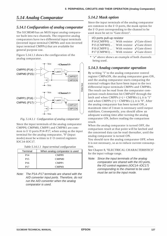
S1C88349 TECHNICAL MANUAL EPSON 127
5 PERIPHERAL CIRCUITS AND THEIR OPERATION (Analog Comparator)
5.14 Analog Comparator
5.14.1 Configuration of analog comparatorThe S1C88349 has an MOS input analog compara-tor built into two channels. The respective analogcomparators have two differential input terminals(inverted input terminal CMPMx and non-invertedinput terminal CMPPx) that are available forgeneral purpose use.
Figure 5.14.1.1 shows the configuration of theanalog comparator.
Fig. 5.14.1.1 Configuration of analog comparator
Since the input terminals of the analog comparatorCMPP0, CMPM0, CMPP1 and CMPM1 are com-mon to I/O ports P14–P17, when using as the inputterminal for the analog comparator, "0" (inputmode) must be written to I/O control registersIOC14–IOC17.
Table 5.14.1.1 Input terminal configuration
Terminal
P14
P15
P16
P17
When analog comparator is used
CMPP0
CMPM0
CMPP1
CMPM1
Dat
a bu
s
CMP0DT
VDD
VSS
CMPP0 (P14)
CMPM0 (P15)
+
–
CMP0ON
CMP1DT
VDD
VSS
CMPP1 (P16)
CMPM1 (P17)
+
–
CMP1ON
Latch
Latch
<Channel 0>
<Channel 1>
Note: The P14–P17 terminals are shared with theA/D converter input ports. Therefore, do notrun the A/D converter when the analogcomparator is used.
5.14.2 Mask optionSince the input terminals of the analog comparatorare common to the I/O ports, the mask option forthe I/O port corresponding to the channel to beused must be set to "Gate direct".
I/O ports pull-up resistorP14 (CMPP0) ... With resistor Gate directP15 (CMPM0) .. With resistor Gate directP16 (CMPP1) ... With resistor Gate directP17 (CMPM1) .. With resistor Gate direct
* " " above shows an example of both channelsbeing used.
5.14.3 Analog comparator operationBy writing "1" to the analog comparator controlregister CMPxON, the analog comparator goes ON,and the analog comparator starts comparing theexternal voltages that have been input to the twodifferential input terminals CMPPx and CMPMx.The result can be read from the comparator com-parison result detection bit CMPxDT through thelatch and when CMPPx (+) > CMPMx (-), it is "1"and when CMPPx (+) < CMPMx (-), it is "0". Afterthe analog comparator has been turned ON, amaximum time of 3 msec is necessary until outputstabilizes. Consequently, you should allow anadequate waiting time after turning the analogcomparator ON, before reading the comparisonresult.When the analog comparator is turned OFF, thecomparison result at that point will be latched andthe concerned data can be read thereafter, until theanalog comparator is turned ON.You should turn the analog comparator OFF, whenit is not necessary, so as to reduce current consump-tion.See Chapter 8, "ELECTRICAL CHARACTERISTICS"for the input voltage range.
Note: Since the input terminals of the analogcomparator are shared with the I/O ports,the I/O control registers (IOC14–IOC17)corresponding to the channel to be usedmust be set to the input mode.
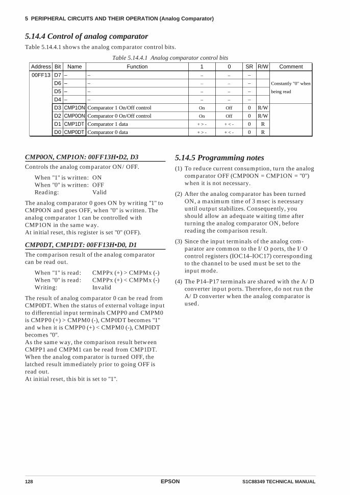
128 EPSON S1C88349 TECHNICAL MANUAL
5 PERIPHERAL CIRCUITS AND THEIR OPERATION (Analog Comparator)
5.14.4 Control of analog comparatorTable 5.14.4.1 shows the analog comparator control bits.
Table 5.14.4.1 Analog comparator control bits
Address Bit Name SR R/WFunction Comment1 0
00FF13 D7
D6
D5
D4
D3
D2
D1
D0
–
–
–
–
CMP1ON
CMP0ON
CMP1DT
CMP0DT
–
–
–
–
Comparator 1 On/Off control
Comparator 0 On/Off control
Comparator 1 data
Comparator 0 data
Constantly "0" when
being read
–
–
–
–
0
0
0
0
R/W
R/W
R
R
–
–
–
–
On
On
+ > -
+ > -
–
–
–
–
Off
Off
+ < -
+ < -
CMP0ON, CMP1ON: 00FF13H•D2, D3Controls the analog comparator ON/OFF.
When "1" is written: ONWhen "0" is written: OFFReading: Valid
The analog comparator 0 goes ON by writing "1" toCMP0ON and goes OFF, when "0" is written. Theanalog comparator 1 can be controlled withCMP1ON in the same way.At initial reset, this register is set "0" (OFF).
CMP0DT, CMP1DT: 00FF13H•D0, D1The comparison result of the analog comparatorcan be read out.
When "1" is read: CMPPx (+) > CMPMx (-)When "0" is read: CMPPx (+) < CMPMx (-)Writing: Invalid
The result of analog comparator 0 can be read fromCMP0DT. When the status of external voltage inputto differential input terminals CMPP0 and CMPM0is CMPP0 (+) > CMPM0 (-), CMP0DT becomes "1"and when it is CMPP0 (+) < CMPM0 (-), CMP0DTbecomes "0".As the same way, the comparison result betweenCMPP1 and CMPM1 can be read from CMP1DT.When the analog comparator is turned OFF, thelatched result immediately prior to going OFF isread out.At initial reset, this bit is set to "1".
5.14.5 Programming notes(1) To reduce current consumption, turn the analog
comparator OFF (CMP0ON = CMP1ON = "0")when it is not necessary.
(2) After the analog comparator has been turnedON, a maximum time of 3 msec is necessaryuntil output stabilizes. Consequently, youshould allow an adequate waiting time afterturning the analog comparator ON, beforereading the comparison result.
(3) Since the input terminals of the analog com-parator are common to the I/O ports, the I/Ocontrol registers (IOC14–IOC17) correspondingto the channel to be used must be set to theinput mode.
(4) The P14–P17 terminals are shared with the A/Dconverter input ports. Therefore, do not run theA/D converter when the analog comparator isused.
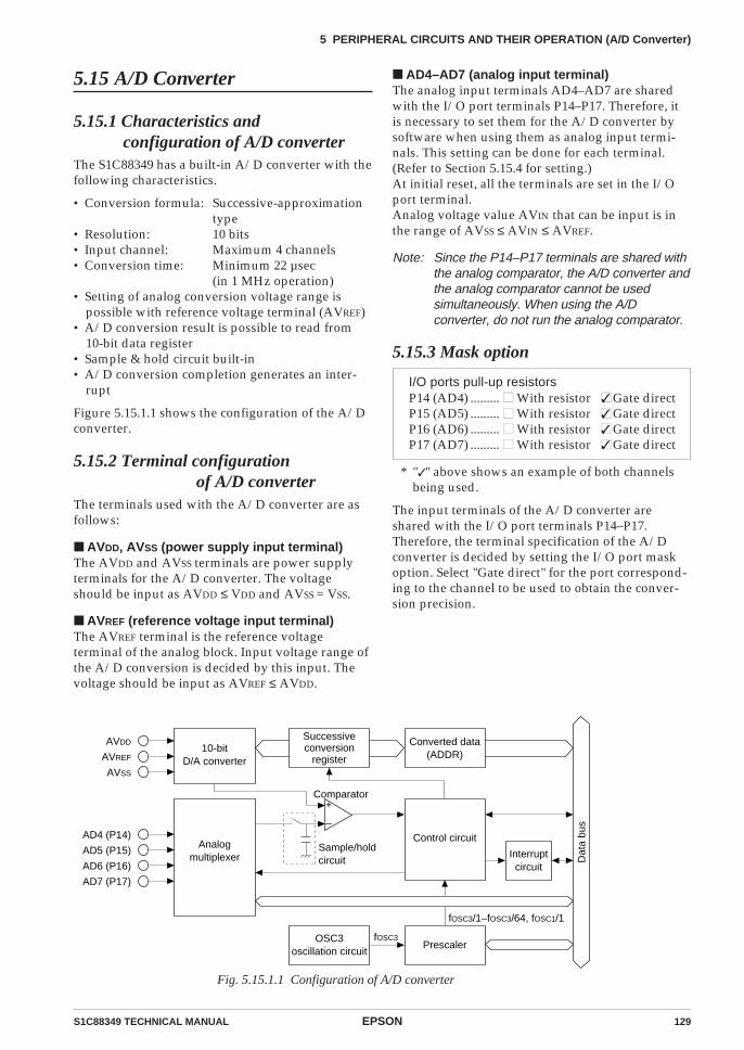
S1C88349 TECHNICAL MANUAL EPSON 129
5 PERIPHERAL CIRCUITS AND THEIR OPERATION (A/D Converter)
5.15 A/D Converter
5.15.1 Characteristics and configuration of A/D converter
The S1C88349 has a built-in A/D converter with thefollowing characteristics.
• Conversion formula: Successive-approximationtype
• Resolution: 10 bits• Input channel: Maximum 4 channels• Conversion time: Minimum 22 µsec
(in 1 MHz operation)• Setting of analog conversion voltage range is
possible with reference voltage terminal (AVREF)• A/D conversion result is possible to read from
10-bit data register• Sample & hold circuit built-in• A/D conversion completion generates an inter-
rupt
Figure 5.15.1.1 shows the configuration of the A/Dconverter.
AD4–AD7 (analog input terminal)The analog input terminals AD4–AD7 are sharedwith the I/O port terminals P14–P17. Therefore, itis necessary to set them for the A/D converter bysoftware when using them as analog input termi-nals. This setting can be done for each terminal.(Refer to Section 5.15.4 for setting.)At initial reset, all the terminals are set in the I/Oport terminal.Analog voltage value AVIN that can be input is inthe range of AVSS ≤ AVIN ≤ AVREF.
Note: Since the P14–P17 terminals are shared withthe analog comparator, the A/D converter andthe analog comparator cannot be usedsimultaneously. When using the A/Dconverter, do not run the analog comparator.
5.15.3 Mask option
I/O ports pull-up resistors
10-bitD/A converter
Dat
a bu
s
AVDD
AVREF
AVSS
Analogmultiplexer
Control circuitAD4 (P14)
AD5 (P15)
AD6 (P16)
AD7 (P17)
Successiveconversion
register
Converted data(ADDR)
OSC3oscillation circuit
Prescaler
Interruptcircuit
+
–
Sample/holdcircuit
Comparator
fOSC3
fOSC3/1–fOSC3/64, fOSC1/1
Fig. 5.15.1.1 Configuration of A/D converter
5.15.2 Terminal configurationof A/D converter
The terminals used with the A/D converter are asfollows:
AVDD, AVSS (power supply input terminal)The AVDD and AVSS terminals are power supplyterminals for the A/D converter. The voltageshould be input as AVDD ≤ VDD and AVSS = VSS.
AVREF (reference voltage input terminal)The AVREF terminal is the reference voltageterminal of the analog block. Input voltage range ofthe A/D conversion is decided by this input. Thevoltage should be input as AVREF ≤ AVDD.
P14 (AD4) ......... With resistor Gate directP15 (AD5) ......... With resistor Gate directP16 (AD6) ......... With resistor Gate directP17 (AD7) ......... With resistor Gate direct
* " " above shows an example of both channelsbeing used.
The input terminals of the A/D converter areshared with the I/O port terminals P14–P17.Therefore, the terminal specification of the A/Dconverter is decided by setting the I/O port maskoption. Select "Gate direct" for the port correspond-ing to the channel to be used to obtain the conver-sion precision.
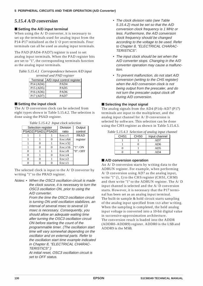
130 EPSON S1C88349 TECHNICAL MANUAL
5 PERIPHERAL CIRCUITS AND THEIR OPERATION (A/D Converter)
5.15.4 A/D conversion
Setting the A/D input terminalWhen using the A/D converter, it is necessary toset up the terminals used for analog input from theP14–P17 initialized as the I/O port terminals. Fourterminals can all be used as analog input terminals.
The PAD (PAD4–PAD7) register is used to setanalog input terminals. When the PAD register bitsare set to "1", the corresponding terminals functionas the analog input terminals.
Table 5.15.4.1 Correspondence between A/D inputterminal and PAD register
TerminalP14 (AD4)P15 (AD5)P16 (AD6)P17 (AD7)
A/D input control registerPAD4PAD5PAD6PAD7
Setting the input clockThe A/D conversion clock can be selected fromeight types shown in Table 5.15.4.2. The selection isdone using the PSAD register.
Table 5.15.4.2 Input clock selectionDivision
ratiofOSC1/1fOSC3/64fOSC3/32fOSC3/16fOSC3/8fOSC3/4fOSC3/2fOSC3/1
OutputcontrolPRADregister
"1": ON"0": OFF
PSAD211110000
Selection registerPSAD1
11001100
PSAD010101010
The selected clock is input to the A/D converter bywriting "1" to the PRAD register.
Notes: • When the OSC3 oscillation circuit is madethe clock source, it is necessary to turn theOSC3 oscillation ON, prior to using theA/D converter.From the time the OSC3 oscillation circuitis turning ON until oscillation stabilizes, aninterval of several msec to several 10msec is necessary. Consequently, youshould allow an adequate waiting timeafter turning the OSC3 oscillation circuitON before starting the count of theprogrammable timer. (The oscillation starttime will vary somewhat depending on theoscillator and on external parts. Refer tothe oscillation start time example indicatedin Chapter 8, "ELECTRICAL CHARAC-TERISTICS".)At initial reset, OSC3 oscillation circuit isset to OFF status.
• The clock division ratio (see Table5.15.4.2) must be set so that the A/Dconversion clock frequency is 1 MHz orless. Furthermore, the A/D conversionclock frequency should be changedaccording to the voltage to be used. Referto Chapter 8, "ELECTRICAL CHARAC-TERISTICS".
• The input clock should be set when theA/D converter stops. Changing in the A/Dconverter operation may cause a malfunc-tion.
• To prevent malfunction, do not start A/Dconversion (writing to the CHS register)when the A/D conversion clock is notbeing output from the prescaler, and donot turn the prescaler output clock offduring A/D conversion.
Selecting the input signalThe analog signals from the AD4 (P14)–AD7 (P17)terminals are input to the multiplexer, and theanalog input channel for A/D conversion isselected by software. This selection can be doneusing the CHS register as shown in Table 5.15.4.3.
Table 5.15.4.3 Selection of analog input channelInput channel
AD7AD6AD5AD4
CHS11100
CHS01010
A/D conversion operationAn A/D conversion starts by writing data to theADRUN register. For example, when performingA/D conversion using AD7 as the analog input,write "1" (1, 1) to the CHS register (CHS1, CHS0)and then write "1" to the ADRUN register. The A/Dinput channel is selected and the A/D conversionstarts. However, it is necessary that the P17 termi-nal has been set as an analog input terminal.The built-in sample & hold circuit starts samplingof the analog input specified from tAD after writing.When the sampling is completed, the held analoginput voltage is converted into a 10-bit digital valuein successive-approximation architecture.The conversion result is loaded into the ADDR(ADDR0–ADDR9) register. ADDR0 is the LSB andADDR9 is the MSB.
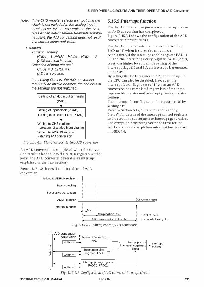
S1C88349 TECHNICAL MANUAL EPSON 131
5 PERIPHERAL CIRCUITS AND THEIR OPERATION (A/D Converter)
Note: If the CHS register selects an input channelwhich is not included in the analog inputterminals set by the PAD register (the PADregister can select several terminals simulta-neously), the A/D conversion does not resultin a correct converted value.
Example)Terminal setting:
PAD5 = 1, PAD7 = PAD6 = PAD4 = 0(AD5 terminal is used)
Selection of input channel:CHS1 = 0, CHS0 = 0(AD4 is selected)
In a setting like this, the A/D conversionresult will be invalid because the contents ofthe settings are not matched.
Setting of input clock (PSAD)
Turning clock output ON (PRAD)
Setting of analog input terminals
(PAD)
Writing to CHS register=selection of analog input channel
Writing to ADRUN register=starting A/D conversion
Fig. 5.15.4.1 Flowchart for starting A/D conversion
An A/D conversion is completed when the conver-sion result is loaded into the ADDR register. At thatpoint, the A/D converter generates an interrupt(explained in the next section).
Figure 5.15.4.2 shows the timing chart of A/Dconversion.
5.15.5 Interrupt functionThe A/D converter can generate an interrupt whenan A/D conversion has completed.Figure 5.15.5.1 shows the configuration of the A/Dconverter interrupt circuit.
The A/D converter sets the interrupt factor flagFAD to "1" when it stores the conversion.At this time, if the interrupt enable register EAD is"1" and the interrupt priority register PADC (2 bits)is set to a higher level than the setting of theinterrupt flags (I0 and I1), an interrupt is generatedto the CPU.By setting the EAD register to "0", the interrupt tothe CPU can also be disabled. However, theinterrupt factor flag is set to "1" when an A/Dconversion has completed regardless of the inter-rupt enable register and interrupt priority registersettings.The interrupt factor flag set in "1" is reset to "0" bywriting "1".Refer to Section 5.17, "Interrupt and StandbyStatus", for details of the interrupt control registersand operations subsequent to interrupt generation.The exception processing vector address for theA/D conversion completion interrupt has been setin 000024H.
Writing to ADRUN register
Input sampling
Successive conversion
ADDR register
Interrupt requesttAD
Sampling time 8tCLK tAD:
tCLK:
0 to 1tCLK
Input clock cycle
Conversion result
A/D conversion time 21tCLK+tAD
Fig. 5.15.4.2 Timing chart of A/D conversion
Dat
a bu
s
Interruptrequest
Address
A/D conversioncompletion Interrupt factor flag
FAD
Address
Interrupt enableregister EAD
Interrupt prioritylevel judgement
circuit
Address
Interrupt priority registerPADC0, PADC1
Fig. 5.15.5.1 Configuration of A/D converter interrupt circuit
132 EPSON S1C88349 TECHNICAL MANUAL
5 PERIPHERAL CIRCUITS AND THEIR OPERATION (A/D Converter)
5.15.6 Control of A/D converterTable 5.15.6.1 shows the A/D converter control bits.
Table 5.15.6.1(a) A/D converter control bits
Address Bit Name SR R/WFunction Comment1 0
00FF80 D7
D6
D5
D4
D3
D2
D1
D0
–
–
–
–
PRAD
PSAD2
PSAD1
PSAD0
–
–
–
–
A/D converter clock control
A/D converter division ratio
Constantly "0" when
being read
–
–
–
–
0
0
0
0
R/W
R/W
R/W
R/W
–
–
–
–
On
–
–
–
–
Off
PSAD2
11110000
PSAD1
11001100
PSAD0
10101010
Division ratio
fOSC1 / 1fOSC3 / 64fOSC3 / 32fOSC3 / 16fOSC3 / 8fOSC3 / 4fOSC3 / 2fOSC3 / 1
00FF81 D7
D6
D5
D4
D3
D2
D1
D0
PAD7
PAD6
PAD5
PAD4
–
–
–
–
P17 A/D converter input control
P16 A/D converter input control
P15 A/D converter input control
P14 A/D converter input control
–
–
–
–
Constantly "0" when
being read
0
0
0
0
–
–
–
–
R/W
R/W
R/W
R/W
A/D
converter
input
–
–
–
–
I/O port
–
–
–
–
00FF82 D7
D6
D5
D4
D3
D2
D1
D0
ADRUN
–
–
–
–
–
CHS1
CHS0
A/D conversion start control register
–
–
–
–
–
Analog input channel selection
Constantly "0" when
being read
0
–
–
–
–
–
0
0
W
R/W
R/W
Start
–
–
–
–
–
Invalid
–
–
–
–
–
CHS1
1
1
0
0
CHS0
1
0
1
0
Input channel
AD7
AD6
AD5
AD4
00FF83 D7
D6
D5
D4
D3
D2
D1
D0
ADDR9
ADDR8
ADDR7
ADDR6
ADDR5
ADDR4
ADDR3
ADDR2
A/D conversion result D9 (MSB)
A/D conversion result D8
A/D conversion result D7
A/D conversion result D6
A/D conversion result D5
A/D conversion result D4
A/D conversion result D3
A/D conversion result D2
– R
00FF84 D7
D6
D5
D4
D3
D2
D1
D0
–
–
–
–
–
–
ADDR1
ADDR0
–
–
–
–
–
–
A/D conversion result D1
A/D conversion result D0 (LSB)
Constantly "0" when
being read
–
–
–
–
–
–
– R
–
–
–
–
–
–
–
–
–
–
–
–
S1C88349 TECHNICAL MANUAL EPSON 133
5 PERIPHERAL CIRCUITS AND THEIR OPERATION (A/D Converter)
Table 5.15.6.1(b) A/D converter control bits
Address Bit Name SR R/WFunction Comment1 0
00FF28 D7
D6
D5
D4
D3
D2
D1
D0
PADC1
PADC0
–
–
–
–
–
–
A/D converter interrupt priority register
Reserved
Reserved
–
–
–
–
Do not write "1".
Constantly "0" when
being read
0
0
0
0
–
–
–
–
R/W
R/W
Prohibited
Prohibited
–
–
–
–
–
–
–
–
–
–
–
PADC11100
PADC01010
PriorityLevel 3Level 2Level 1Level 0
00FF2A D7
D6
D5
D4
D3
D2
D1
D0
EAD
–
–
–
–
–
–
–
A/D converter interrupt enable register
Reserved
–
–
–
–
–
–
Constantly "0" when
being read
0
0
–
–
–
–
–
–
R/W
R/W
Enable
–
–
–
–
–
–
–
Disable
–
–
–
–
–
–
–
00FF2C D7
D6
D5
D4
D3
D2
D1
D0
FAD
–
–
–
–
–
–
–
A/D converter interrupt factor flag
Reserved
–
–
–
–
–
–
Constantly "0" when
being read
0
0
–
–
–
–
–
–
R/W
R/W
Generated
Reset
R)
W)
Not generated
No operation
–
–
–
–
–
–
–
–
–
–
–
–
–
–
PAD4–PAD7: 00FF81H•D4–D7Sets the P14–P17 terminals as the analog inputterminals for the A/D converter.
When "1" is written: A/D converter inputWhen "0" is written: I/O portReading: Valid
When "1" is written to PADn, the P1n terminal is setto the analog input terminal ADn. (n=4–7)When "0" is written, the terminal is used with the I/O port.At initial reset, this register is set to "0" (I/O port).
PSAD0–PSAD2: 00FF80H•D0–D2Selects the clock for the A/D converter.
Table 5.15.6.2 Input clock selectionDivision
ratiofOSC1/1fOSC3/64fOSC3/32fOSC3/16fOSC3/8fOSC3/4fOSC3/2fOSC3/1
OutputcontrolPRADregister
"1": ON"0": OFF
PSAD211110000
Selection registerPSAD1
11001100
PSAD010101010
This setting controls the division ratio of theprescaler.At initial reset, this register is set to "0" (fOSC3/1).

134 EPSON S1C88349 TECHNICAL MANUAL
5 PERIPHERAL CIRCUITS AND THEIR OPERATION (A/D Converter)
PRAD: 00FF80H•D3Controls the clock supply to the A/D converter.
When "1" is written: ONWhen "0" is written: OFFReading: Invalid
By writing "1" to the PRAD register, the clockselected with the PSAD register is input to the A/Dconverter.When "0" is written, the clock is not input to theA/D converter.At initial reset, this register is set to "0" (OFF).
ADRUN: 00FF82H•D7Starts A/D conversion.
When "1" is written: Start A/D conversionWhen "0" is written: InvalidReading: Always "0"
By writing "1" to this register, the A/D converterstarts A/D conversion of the channel selected bythe CHS register, and stores the conversion result tothe ADDR register.
CHS0, CHS1: 00FF82H•D0, D1Selects an analog input channel.
Table 5.15.6.3 Selection of analog input channelInput channel
AD7AD6AD5AD4
CHS11100
CHS01010
At initial reset, this register is set to "0" (AD4).
ADDR0–ADDR9: 00FF84H•D0, D1, 00FF83HA/D conversion result is stored.ADDR0 is the LSB and ADDR9 is the MSB.ADDR0 and ADDR1 are assigned in D0 bit and D1bit of the address 00FF84H. D2–D7 bits in thisaddress are always "0" when being read.At initial reset, data is undefined.
PADC0, PADC1: 00FF28H•D6, D7Sets the priority level of the A/D conversioncompletion interrupt.Table 5.15.6.4 shows the interrupt priority levelwhich can be set by the PADC register.
Table 5.15.6.4 Interrupt priority level settings
PADC1
1
1
0
0
Interrupt priority level
Level 3
Level 2
Level 1
Level 0
PADC0
1
0
1
0
(IRQ3)
(IRQ2)
(IRQ1)
(None)
At initial reset, this register is set to "0" (level 0).
EAD: 00FF2AH•D7Enables or disables the A/D conversion completioninterrupt generation to the CPU.
When "1" is written: Interrupt is enabledWhen "0" is written: Interrupt is disabledReading: Valid
The EAD register is the interrupt enable registercorresponding to the A/D conversion completioninterrupt factor. When this register is set to "1", theinterrupt is enabled, and when it is set to "0", theinterrupt is disabled.At initial reset, this register is set to "0" (interrupt isdisabled).
FAD: 00FF2CH•D7Indicates the generation of A/D conversioncompletion interrupt factor.
When "1" is read: Int. factor has generatedWhen "0" is read: Int. factor has not generated
When "1" is written: Factor flag is resetWhen "0" is written: Invalid
FAD is the interrupt factor flag corresponding tothe A/D conversion completion interrupt. It is setto "1" when an A/D conversion is completed.At this point, if the corresponding interrupt enableregister is set to "1" and the corresponding interruptpriority register is set to a higher level than thesetting of the interrupt flags (I0 and I1), an interruptis generated to the CPU.Regardless of the interrupt enable register andinterrupt priority register settings, the interruptfactor flag is set to "1" when the interrupt genera-tion condition is met.To accept the subsequent interrupt after an inter-rupt generation, it is necessary to re-set the inter-rupt flags (set the interrupt flag to a lower levelthan the level indicated by the interrupt priorityregisters, or execute the RETE instruction) and toreset the interrupt factor flag. The interrupt factorflag is reset to "0" by writing "1".At initial reset, the FAD flag is reset to "0".
S1C88349 TECHNICAL MANUAL EPSON 135
5 PERIPHERAL CIRCUITS AND THEIR OPERATION (A/D Converter)
5.15.7 Programming notes(1) When the OSC3 oscillation circuit is made the
clock source, it is necessary to turn the OSC3oscillation ON, prior to using the A/D con-verter.From the time the OSC3 oscillation circuit isturning ON until oscillation stabilizes, aninterval of several msec to several 10 msec isnecessary. Consequently, you should allow anadequate waiting time after turning the OSC3oscillation circuit ON before starting the countof the programmable timer. (The oscillationstart time will vary somewhat depending on theoscillator and on external parts. Refer to theoscillation start time example indicated inChapter 8, "ELECTRICAL CHARACTERIS-TICS".)At initial reset, OSC3 oscillation circuit is set toOFF status.
(2) When SLEEP mode is set during A/D conver-sion, correct A/D conversion result cannot beobtained because the OSC3 oscillation circuitstops. Do not set in SLEEP mode during A/Dconversion.
(3) The input clock and analog input terminalsshould be set when the A/D converter stops.Changing in the A/D converter operation maycause a malfunction.
(4) The clock division ratio (see Table 5.15.4.2) mustbe set so that the A/D conversion clock fre-quency is 1 MHz or less. Furthermore, the A/Dconversion clock frequency should be changedaccording to the voltage to be used. Refer toChapter 8, "ELECTRICAL CHARACTERIS-TICS".
(5) To prevent malfunction, do not start A/Dconversion (writing to the CHS register) whenthe A/D conversion clock is not being outputfrom the prescaler, and do not turn the prescaleroutput clock off during A/D conversion.
(6) If the CHS register selects an input channelwhich is not included in the analog inputterminals set by the PAD register (the PADregister can select several terminals simulta-neously), the A/D conversion does not result ina correct converted value.
(7) During A/D conversion, do not operate the P1nterminals which are not used for analog inputsof the A/D converter (for input/output ofdigital signal). It affects the A/D conversionprecision.
(8) Since the P14–P17 terminals are shared with theanalog comparator, the A/D converter and theanalog comparator cannot be used simulta-neously. When using the A/D converter, do notrun the analog comparator.
(9) Note that writing "1" to the A/D convertercontrol bits (FF28H•D5, D4) may cause a mal-function.
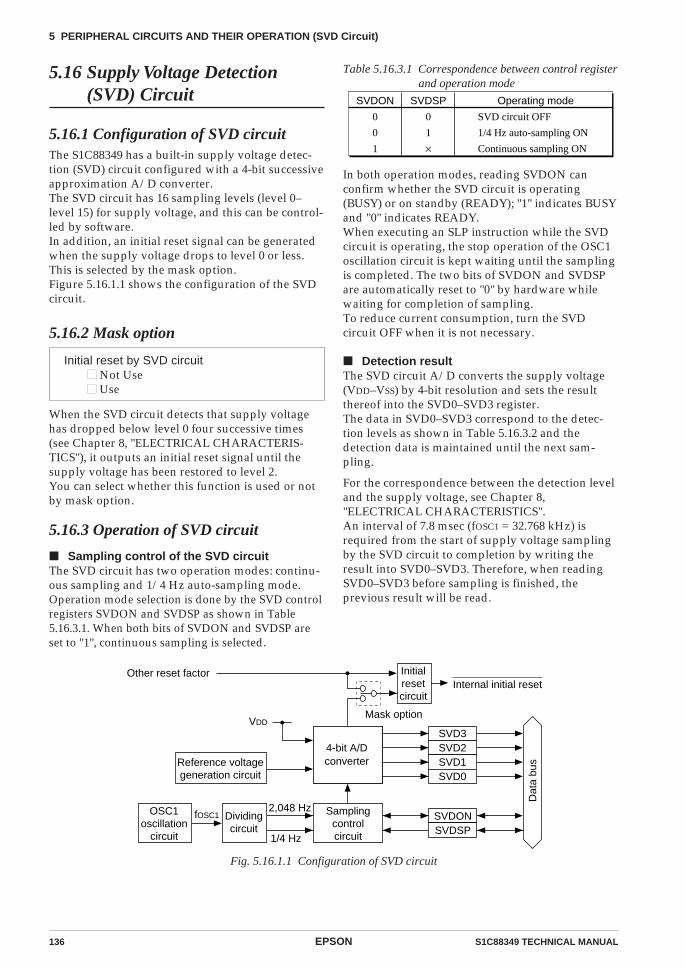
136 EPSON S1C88349 TECHNICAL MANUAL
5 PERIPHERAL CIRCUITS AND THEIR OPERATION (SVD Circuit)
5.16 Supply Voltage Detection(SVD) Circuit
5.16.1 Configuration of SVD circuitThe S1C88349 has a built-in supply voltage detec-tion (SVD) circuit configured with a 4-bit successiveapproximation A/D converter.The SVD circuit has 16 sampling levels (level 0–level 15) for supply voltage, and this can be control-led by software.In addition, an initial reset signal can be generatedwhen the supply voltage drops to level 0 or less.This is selected by the mask option.Figure 5.16.1.1 shows the configuration of the SVDcircuit.
In both operation modes, reading SVDON canconfirm whether the SVD circuit is operating(BUSY) or on standby (READY); "1" indicates BUSYand "0" indicates READY.When executing an SLP instruction while the SVDcircuit is operating, the stop operation of the OSC1oscillation circuit is kept waiting until the samplingis completed. The two bits of SVDON and SVDSPare automatically reset to "0" by hardware whilewaiting for completion of sampling.To reduce current consumption, turn the SVDcircuit OFF when it is not necessary.
Detection resultThe SVD circuit A/D converts the supply voltage(VDD–VSS) by 4-bit resolution and sets the resultthereof into the SVD0–SVD3 register.The data in SVD0–SVD3 correspond to the detec-tion levels as shown in Table 5.16.3.2 and thedetection data is maintained until the next sam-pling.
For the correspondence between the detection leveland the supply voltage, see Chapter 8,"ELECTRICAL CHARACTERISTICS".An interval of 7.8 msec (fOSC1 = 32.768 kHz) isrequired from the start of supply voltage samplingby the SVD circuit to completion by writing theresult into SVD0–SVD3. Therefore, when readingSVD0–SVD3 before sampling is finished, theprevious result will be read.
Fig. 5.16.1.1 Configuration of SVD circuit
VDD
Dat
a bu
s
SVD3SVD2SVD1SVD0
2,048 Hz Samplingcontrolcircuit
SVDONSVDSP
Mask option
fOSC1 Dividingcircuit
OSC1oscillation
circuit
Reference voltagegeneration circuit
Internal initial resetOther reset factor Initial
resetcircuit
1/4 Hz
4-bit A/Dconverter
SVDON
0
0
1
Operating mode
SVD circuit OFF
1/4 Hz auto-sampling ON
Continuous sampling ON
SVDSP
0
1
×
Table 5.16.3.1 Correspondence between control registerand operation mode
5.16.2 Mask option
Initial reset by SVD circuit Not Use Use
When the SVD circuit detects that supply voltagehas dropped below level 0 four successive times(see Chapter 8, "ELECTRICAL CHARACTERIS-TICS"), it outputs an initial reset signal until thesupply voltage has been restored to level 2.You can select whether this function is used or notby mask option.
5.16.3 Operation of SVD circuit
Sampling control of the SVD circuitThe SVD circuit has two operation modes: continu-ous sampling and 1/4 Hz auto-sampling mode.Operation mode selection is done by the SVD controlregisters SVDON and SVDSP as shown in Table5.16.3.1. When both bits of SVDON and SVDSP areset to "1", continuous sampling is selected.

S1C88349 TECHNICAL MANUAL EPSON 137
5 PERIPHERAL CIRCUITS AND THEIR OPERATION (SVD Circuit)
Table 5.16.3.2 Supply voltage detection results The SVD circuit starts operation in synchroniza-tion with the internal 2,048 Hz signal andperforms one sampling in 16 clock cycles.The sampling is done continuously withoutsetting the standby time and the result islatched to SVD0–SVD3 in every 16 clock cycles.Cancellation of continuous sampling is done bywriting "0" to SVDON. The SVD circuit main-tains ON status until completion of samplingand then goes OFF.After writing "0" to SVDON, SVDON reads "1"until the SVD circuit actually goes OFF.Figure 5.16.3.1 shows the timing chart of thecontinuous sampling.
(2) 1/4 Hz auto-sampling modeThis mode is selected when "0" is written toSVDON and "1" is written to SVDSP. In thiscase, supply voltage sampling is done in every 4seconds.The sampling time is 7.8 msec as in continuoussampling, and the result in SVD0–SVD3 isupdated every 4 seconds.Cancellation of 1/4 Hz auto-sampling is doneby writing "0" to SVDSP. If the SVD circuit issampling, SVD circuit waits until completionand then turns OFF. In addition, "1" is read fromSVDON while the SVD circuit is sampling.Figure 5.16.3.2 shows the timing chart of the 1/4Hz auto-sampling.
Timing of samplingNext, we will explain the timing for two operationmodes.
(1) Continuous sampling modeThis mode is selected when "1" is written toSVDON and sampling of the supply voltage isdone continuously in 7.8 msec cycles.
Fig. 5.16.3.1 Timing chart of continuous sampling
SVD0–SVD3
1 Hz
SVDSP(W)
SVDON(R)
Sampling (7.8 msec)
Standby status
4 sec
Fig. 5.16.3.2 Timing chart of 1/4 Hz auto-sampling
SVD3 SVD0 Detection level
1
1
1
1
1
1
1
1
0
0
0
0
0
0
0
0
1
0
1
0
1
0
1
0
1
0
1
0
1
0
1
0
Level 15
Level 14
Level 13
Level 12
Level 11
Level 10
Level 9
Level 8
Level 7
Level 6
Level 5
Level 4
Level 3
Level 2
Level 1
Level 0
SVD1
1
1
0
0
1
1
0
0
1
1
0
0
1
1
0
0
SVD2
1
1
1
1
0
0
0
0
1
1
1
1
0
0
0
0
SVD0–SVD3
2,048 Hz
SVDON(W)
Latch
Sampling (7.8 msec)
SVDON(R)
(0)(1)
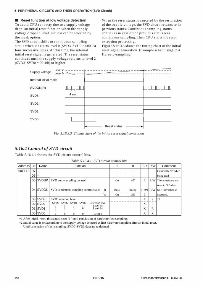
138 EPSON S1C88349 TECHNICAL MANUAL
5 PERIPHERAL CIRCUITS AND THEIR OPERATION (SVD Circuit)
Reset function at low voltage detectionTo avoid CPU runaway due to a supply voltagedrop, an initial reset function when the supplyvoltage drops to level 0 or less can be selected bythe mask option.The SVD circuit shifts to continuous samplingstatus when it detects level 0 (SVD3–SVD0 = 0000B)four successive times. At this time, the internalinitial reset signal is generated. The reset statuscontinues until the supply voltage returns to level 2(SVD3–SVD0 = 0010B) or higher.
When the reset status is canceled by the restorationof the supply voltage, the SVD circuit returns to itsprevious status. Continuous sampling statuscontinues in case of the previous status wascontinuous sampling. Then CPU starts the resetexception processing.Figure 5.16.3.3 shows the timing chart of the initialreset signal generation. (Example when using 1/4Hz auto-sampling.)
Supply voltage
Internal initial reset
SVDON(R)
SVD3
SVD2
SVD1
SVD0
Level 2Level 0
Reset status
4 sec
Fig. 5.16.3.3 Timing chart of the initial reset signal generation
5.16.4 Control of SVD circuitTable 5.16.4.1 shows the SVD circuit control bits.
Table 5.16.4.1 SVD circuit control bits
Address Bit Name SR R/WFunction Comment1 0
00FF12 D7
D6
D5
D4
D3
D2
D1
D0
–
–
SVDSP
SVDON
SVD3
SVD2
SVD1
SVD0
–
–
SVD auto-sampling control
SVD continuous sampling control/status
SVD detection level
Constantly "0" when
being read
These registers are
reset to "0" when
SLP instruction is
executed.
*2
–
–
0
1→0*1
0
X
X
X
X
R/W
R/W
R
R
R
R
–
–
On
Busy
On
–
–
Off
Ready
Off
R
W
SVD311:0
SVD211:0
SVD111:0
SVD010:0
Detection levelLevel 15Level 14
:Level 0
*1 After initial reset, this status is set "1" until conclusion of hardware first sampling.*2 Initial value is set according to the supply voltage detected at first hardware sampling after an initial reset. Until conclusion of first sampling, SVD0–SVD3 data are undefined.
S1C88349 TECHNICAL MANUAL EPSON 139
5 PERIPHERAL CIRCUITS AND THEIR OPERATION (SVD Circuit)
SVDON: 00FF12H•D4Controls the turning ON/OFF of the continuoussampling mode.
When "1" is written: Continuous sampling ONWhen "0" is written: Continuous sampling OFF
When "1" is read: BUSYWhen "0" is read: READY
The continuous sampling mode goes ON when "1"is written to SVDON and goes OFF, when "0" iswritten.In the ON status, sampling of the supply voltage isdone continuously in 7.8 msec cycles and thedetection result is latched to SVD0–SVD3.SVDON can be read, and "1" indicates SVD circuitoperation (BUSY) and "0" indicates standby(READY).At initial reset and in the SLEEP status, SVDON isset to "0" (continuous sampling OFF/READY).
SVDSP: 00FF12H•D5Controls the turning ON/OFF of the 1/4 Hz auto-sampling mode.
When "1" is written: Auto-sampling ONWhen "0" is written: Auto-sampling OFFReading: Valid
The 1/4 Hz auto-sampling mode goes ON when "1"is written to SVDSP and goes OFF, when "0" iswritten.In the ON status, sampling is done in every 4seconds and "1" is read from SVDON during theactual sampling period (7.8 msec).At initial reset and in the SLEEP status, SVDSP isset to "0" (auto-sampling OFF).
SVD0–SVD3: 00FF12H•D0–D3The detection result of the SVD is set.The reading data correspond to the detection levelsas shown in Table 5.16.4.2 and the data is main-tained until the next sampling.
Table 5.16.4.2 Supply voltage detection results
For the correspondence between the detection leveland the supply voltage, see Chapter 8,"ELECTRICAL CHARACTERISTICS".The initial value at initial reset is set according tothe supply voltage detected at first sampling byhardware. Data of this bit is undefined until thissampling is completed.
5.16.5 Programming notes(1) To reduce current consumption, turn the SVD
circuit OFF (SVDON = SVDSP = "0") when it isnot necessary.
(2) When executing an SLP instruction while theSVD circuit is operating, the stop operation ofthe OSC1 oscillation circuit is kept waiting untilthe sampling is completed. The two bits ofSVDON and SVDSP are automatically reset to"0" by hardware while waiting for completion ofsampling.
SVD3 SVD0 Detection level
1
1
1
1
1
1
1
1
0
0
0
0
0
0
0
0
1
0
1
0
1
0
1
0
1
0
1
0
1
0
1
0
Level 15
Level 14
Level 13
Level 12
Level 11
Level 10
Level 9
Level 8
Level 7
Level 6
Level 5
Level 4
Level 3
Level 2
Level 1
Level 0
SVD1
1
1
0
0
1
1
0
0
1
1
0
0
1
1
0
0
SVD2
1
1
1
1
0
0
0
0
1
1
1
1
0
0
0
0
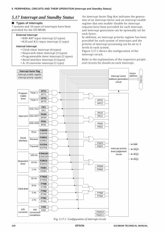
140 EPSON S1C88349 TECHNICAL MANUAL
5 PERIPHERAL CIRCUITS AND THEIR OPERATION (Interrupt and Standby Status)
5.17 Interrupt and Standby Status Types of interrupts7 systems and 16 types of interrupts have beenprovided for the S1C88349.
External interrupt•K00–K07 input interrupt (2 types)•K10 and K11 input interrupt (1 type)
Internal interrupt•Clock timer interrupt (4 types)•Stopwatch timer interrupt (3 types)•Programmable timer interrupt (2 types)•Serial interface interrupt (3 types)•A/D converter interrupt (1 type)
An interrupt factor flag that indicates the genera-tion of an interrupt factor and an interrupt enableregister that sets enable/disable for interruptrequests have been provided for each interruptand interrupt generation can be optionally set foreach factor.In addition, an interrupt priority register has beenprovided for each system of interrupts and thepriority of interrupt processing can be set to 3levels in each system.Figure 5.17.1 shows the configuration of theinterrupt circuit.
Refer to the explanations of the respective periph-eral circuits for details on each interrupt.
Fig. 5.17.1 Configuration of interrupt circuit
FTM32ETM32
32 Hz
FTM8ETM8
8 Hz
FTM2ETM2
2 Hz
FTM1ETM1
1 Hz
Clock timer
FSW100ESW100
100 Hz
FSW10ESW10
10 Hz
FSW1ESW1
1 Hz
Stopwatchtimer
FADEADA/D
conversioncompletion
A/Dconverter
FSERRESERR
Error
FSRECESREC
Receive
FSTRAESTRA
Transmit
Serialinterface
FPT1EPT1
Timer 1
FPT0EPT0
Timer 0
Program-mabletimer
FK1EK1
K10, K11
FK0HEK0H
K04–K07
FK0LEK0L
K00–K03
Input port
PTM0PTM1
PADC0PADC1
PSW0PSW1
PSIF0PSIF1
PK00PK01
PPT0PPT1
Interrupt vectoraddress generation
circuit
NMI
IRQ3
IRQ2
IRQ1
Dat
a bu
s
Vectoraddress
Interrupt prioritylevel judgement
circuit
Interrupt factor flagInterrupt enable registerInterrupt priority register
PK10PK11

S1C88349 TECHNICAL MANUAL EPSON 141
5 PERIPHERAL CIRCUITS AND THEIR OPERATION (Interrupt and Standby Status)
HALT statusBy executing the program's HALT instruction, theS1C88349 shifts to the HALT status.Since CPU operation stops in the HALT status,power consumption can be reduced with onlyperipheral circuit operation.Cancellation of the HALT status is done by initialreset or an optional interrupt request, and the CPUrestarts program execution from an exceptionprocessing routine.See the "S1C88 Core CPU Manual" for the HALTstatus and reactivation sequence.
SLEEP statusBy executing the program's SLP instruction, theS1C88349 shifts to the SLEEP status.Since the operation of the CPU and peripheral circuitsstop completely in the SLEEP status, power consump-tion can be reduced even more than in the HALT status.Cancellation of the SLEEP status is done by initialreset or an input interrupt from the input port. TheCPU reactivates after waiting 8,192/fOSC1 secondsof oscillation stabilization time. At this time, theCPU restarts program execution from an exceptionprocessing routine (input interrupt routine).
Note: Since oscillation is unstable for a short timeafter reactivation from the SLEEP status, thewait time is not always 250 msec even whenusing the 32.768 kHz crystal oscillator forthe OSC1 oscillation circuit.
5.17.1 Interrupt generation conditionsThe interrupt factor flags that indicate the generationof their respective interrupt factors are provided forthe previously indicated 7 systems and 16 types ofinterrupts and they will be set to "1" by the genera-tion of a factor.
In addition, interrupt enable registers with a 1 to 1correspondence to each of the interrupt factor flagsare provided. An interrupt is enabled when "1" iswritten and interrupt is disabled when "0" is written.
The CPU manages the enable/disable of interruptrequests at the interrupt priority level. An interruptpriority register that sets the priority level isprovided for each of the interrupts of the 7 systemsand the CPU accepts only interrupts above the levelthat has been indicated with the interrupt flags (I0and I1).Consequently, the following three conditions arenecessary for the CPU to accept the interrupt.
(1) The interrupt factor flag has been set to "1" bygeneration of an interrupt factor.
(2) The interrupt enable register corresponding tothe above has been set to "1".
(3) The interrupt priority register corresponding tothe above has been set to a priority level higherthan the interrupt flag (I0 and I1) setting.
The CPU initially samples the interrupt for the firstop-code fetch cycle of each instruction. Thereupon,the CPU shifts to the exception processing when theabove mentioned conditions have been established.See the "S1C88 Core CPU Manual" for the exceptionprocessing sequence.
5.17.2 Interrupt factor flagTable 5.17.2.1 shows the correspondence betweenthe factors generating an interrupt and the inter-rupt factor flags.The corresponding interrupt factor flags are set to"1" by generation of the respective interrupt factors.The corresponding interrupt factor can be con-firmed by reading the flags through software.
Table 5.17.2.1 Interrupt factors
FPT1
FPT0
FK1
FK0H
FK0L
FSERR
FSREC
FSTRA
FSW100
FSW10
FSW1
FTM32
FTM8
FTM2
FTM1
FAD
Programmable timer 1 underflow
Programmable timer 0 underflow
Non matching of the K10 and K11 inputs and the input comparison registers KCP10 and KCP11
Non matching of the K04–K07 inputs and the input comparison registers KCP04–KCP07
Non matching of the K00–K03 inputs and the input comparison registers KCP00–KCP03
Serial interface receiving error (in asynchronous mode)
Serial interface receiving completion
Serial interface transmitting completion
Falling edge of the stopwatch timer 100 Hz signal
Falling edge of the stopwatch timer 10 Hz signal
Falling edge of the stopwatch timer 1 Hz signal
Rising edge of the clock timer 32 Hz signal
Rising edge of the clock timer 8 Hz signal
Rising edge of the clock timer 2 Hz signal
Rising edge of the clock timer 1 Hz signal
A/D conversion completion
Interrupt factor Interrupt factor flag
(00FF25 D7)
(00FF25 D6)
(00FF25 D5)
(00FF25 D4)
(00FF25 D3)
(00FF25 D2)
(00FF25 D1)
(00FF25 D0)
(00FF24 D6)
(00FF24 D5)
(00FF24 D4)
(00FF24 D3)
(00FF24 D2)
(00FF24 D1)
(00FF24 D0)
(00FF2C D7)

142 EPSON S1C88349 TECHNICAL MANUAL
5 PERIPHERAL CIRCUITS AND THEIR OPERATION (Interrupt and Standby Status)
Interrupt factor flag that has been set to "1" is resetto "0" by writing "1".At initial reset, the interrupt factor flags are reset to "0".
Note: When executing the RETE instructionwithout resetting the interrupt factor flag afteran interrupt has been generated, the sameinterrupt will be generated. Consequently,the interrupt factor flag corresponding to thatroutine must be reset (writing "1") in theinterrupt processing routine.
5.17.3 Interrupt enable registerThe interrupt enable register has a 1 to 1 corre-spondence with each interrupt factor flag andenable/disable of interrupt requests can be set.
When "1" is written to the interrupt enable register,an interrupt request is enabled, and is disabledwhen "0" is written. This register also permitsreading, thus making it possible to confirm that astatus has been set.At initial reset, the interrupt enable registers are setto "0" and shifts to the interrupt disable status.Table 5.17.3.1 shows the correspondence between theinterrupt enable registers and the interrupt factor flags.
5.17.4 Interrupt priority register andinterrupt priority level
The interrupt priority registers shown in Table5.17.4.1 are set to each system of interrupts and theinterrupt priority levels for the CPU can be set tothe optional priority level (0–3). As a result, it ispossible to have multiple interrupts that match thesystem's interrupt processing priority levels.
The interrupt priority level between each systemcan optionally be set to three levels by the interruptpriority register. However, when more than onesystem is set to the same priority level, they areprocessed according to the default priority level.
Table 5.17.4.2 Setting of interrupt priority level
Table 5.17.3.1 Interrupt enable registers and interrupt factor flags
P*1 P*0 Interrupt priority level
1
1
0
0
1
0
1
0
Level 3 (IRQ3)
Level 2 (IRQ2)
Level 1 (IRQ1)
Level 0 (non)
Table 5.17.4.1 Interrupt priority register
EPT1
EPT0
EK1
EK0H
EK0L
ESERR
ESREC
ESTRA
ESW100
ESW10
ESW1
ETM32
ETM8
ETM2
ETM1
EAD
Programmable timer 1
Programmable timer 0
K10 and K11 input
K04–K07 input
K00–K03 input
Serial interface receiving error
Serial interface receiving completion
Serial interface transmitting completion
Stopwatch timer 100 Hz
Stopwatch timer 10 Hz
Stopwatch timer 1 Hz
Clock timer 32 Hz
Clock timer 8 Hz
Clock timer 2 Hz
Clock timer 1 Hz
A/D conversion completion
Interrupt Interrupt enable register
(00FF23 D7)
(00FF23 D6)
(00FF23 D5)
(00FF23 D4)
(00FF23 D3)
(00FF23 D2)
(00FF23 D1)
(00FF23 D0)
(00FF22 D6)
(00FF22 D5)
(00FF22 D4)
(00FF22 D3)
(00FF22 D2)
(00FF22 D1)
(00FF22 D0)
(00FF2A D7)
FPT1
FPT0
FK1
FK0H
FK0L
FSERR
FSREC
FSTRA
FSW100
FSW10
FSW1
FTM32
FTM8
FTM2
FTM1
FAD
Interrupt factor flag
(00FF25 D7)
(00FF25 D6)
(00FF25 D5)
(00FF25 D4)
(00FF25 D3)
(00FF25 D2)
(00FF25 D1)
(00FF25 D0)
(00FF24 D6)
(00FF24 D5)
(00FF24 D4)
(00FF24 D3)
(00FF24 D2)
(00FF24 D1)
(00FF24 D0)
(00FF2C D7)
Programmable timer interrupt
K10 and K11 input interrupt
K00–K07 input interrupt
Serial interface interrupt
Stopwatch timer interrupt
Clock timer interrupt
A/D converter interrupt
Interrupt
PPT0, PPT1
PK10, PK11
PK00, PK01
PSIF0, PSIF1
PSW0, PSW1
PTM0, PTM1
PADC0, PADC1
Interrupt priority register
(00FF21 D2, D3)
(00FF21 D0, D1)
(00FF20 D6, D7)
(00FF20 D4, D5)
(00FF20 D2, D3)
(00FF20 D0, D1)
(00FF28 D6, D7)
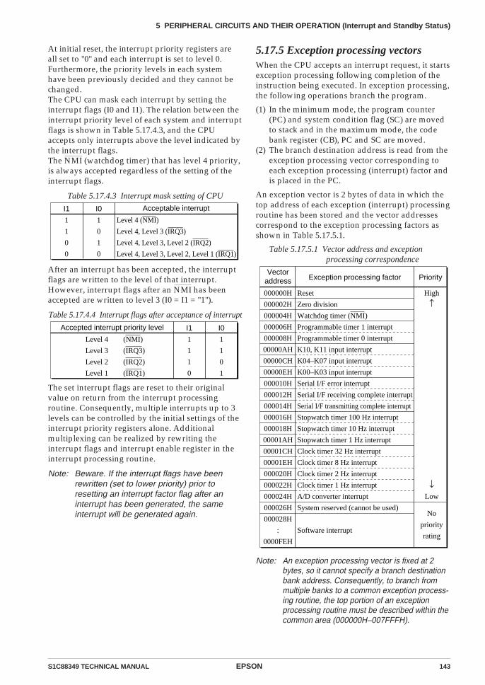
S1C88349 TECHNICAL MANUAL EPSON 143
5 PERIPHERAL CIRCUITS AND THEIR OPERATION (Interrupt and Standby Status)
At initial reset, the interrupt priority registers areall set to "0" and each interrupt is set to level 0.Furthermore, the priority levels in each systemhave been previously decided and they cannot bechanged.The CPU can mask each interrupt by setting theinterrupt flags (I0 and I1). The relation between theinterrupt priority level of each system and interruptflags is shown in Table 5.17.4.3, and the CPUaccepts only interrupts above the level indicated bythe interrupt flags.The NMI (watchdog timer) that has level 4 priority,is always accepted regardless of the setting of theinterrupt flags.
Table 5.17.4.3 Interrupt mask setting of CPU
I1 I0 Acceptable interrupt
1
1
0
0
1
0
1
0
Level 4 (NMI)
Level 4, Level 3 (IRQ3)
Level 4, Level 3, Level 2 (IRQ2)
Level 4, Level 3, Level 2, Level 1 (IRQ1)
After an interrupt has been accepted, the interruptflags are written to the level of that interrupt.However, interrupt flags after an NMI has beenaccepted are written to level 3 (I0 = I1 = "1").
Table 5.17.4.4 Interrupt flags after acceptance of interrupt
5.17.5 Exception processing vectorsWhen the CPU accepts an interrupt request, it startsexception processing following completion of theinstruction being executed. In exception processing,the following operations branch the program.
(1) In the minimum mode, the program counter(PC) and system condition flag (SC) are movedto stack and in the maximum mode, the codebank register (CB), PC and SC are moved.
(2) The branch destination address is read from theexception processing vector corresponding toeach exception processing (interrupt) factor andis placed in the PC.
An exception vector is 2 bytes of data in which thetop address of each exception (interrupt) processingroutine has been stored and the vector addressescorrespond to the exception processing factors asshown in Table 5.17.5.1.
Table 5.17.5.1 Vector address and exception processing correspondence
I1 I0Accepted interrupt priority level
1
1
1
0
1
1
0
1
Level 4 (NMI)
Level 3 (IRQ3)
Level 2 (IRQ2)
Level 1 (IRQ1)
The set interrupt flags are reset to their originalvalue on return from the interrupt processingroutine. Consequently, multiple interrupts up to 3levels can be controlled by the initial settings of theinterrupt priority registers alone. Additionalmultiplexing can be realized by rewriting theinterrupt flags and interrupt enable register in theinterrupt processing routine.
Note: Beware. If the interrupt flags have beenrewritten (set to lower priority) prior toresetting an interrupt factor flag after aninterrupt has been generated, the sameinterrupt will be generated again.
Vectoraddress
000000H
000002H
000004H
000006H
000008H
00000AH
00000CH
00000EH
000010H
000012H
000014H
000016H
000018H
00001AH
00001CH
00001EH
000020H
000022H
000024H
000026H
000028H
:
0000FEH
Priority
High
↑
↓Low
No
priority
rating
Exception processing factor
Reset
Zero division
Watchdog timer (NMI)
Programmable timer 1 interrupt
Programmable timer 0 interrupt
K10, K11 input interrupt
K04–K07 input interrupt
K00–K03 input interrupt
Serial I/F error interrupt
Serial I/F receiving complete interrupt
Serial I/F transmitting complete interrupt
Stopwatch timer 100 Hz interrupt
Stopwatch timer 10 Hz interrupt
Stopwatch timer 1 Hz interrupt
Clock timer 32 Hz interrupt
Clock timer 8 Hz interrupt
Clock timer 2 Hz interrupt
Clock timer 1 Hz interrupt
A/D converter interrupt
System reserved (cannot be used)
Software interrupt
Note: An exception processing vector is fixed at 2bytes, so it cannot specify a branch destinationbank address. Consequently, to branch frommultiple banks to a common exception process-ing routine, the top portion of an exceptionprocessing routine must be described within thecommon area (000000H–007FFFH).
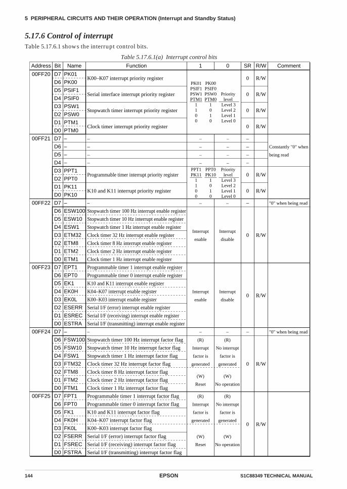
144 EPSON S1C88349 TECHNICAL MANUAL
5 PERIPHERAL CIRCUITS AND THEIR OPERATION (Interrupt and Standby Status)
5.17.6 Control of interruptTable 5.17.6.1 shows the interrupt control bits.
Table 5.17.6.1(a) Interrupt control bits
Address Bit Name SR R/WFunction Comment1 0
00FF20 D7
D6
D5
D4
D3
D2
D1
D0
PK01
PK00
PSIF1
PSIF0
PSW1
PSW0
PTM1
PTM0
K00–K07 interrupt priority register
Serial interface interrupt priority register
Stopwatch timer interrupt priority register
Clock timer interrupt priority register
0
0
0
0
R/W
R/W
R/W
R/W
PK01PSIF1PSW1PTM1
1100
PK00PSIF0PSW0PTM0
1010
Prioritylevel
Level 3Level 2Level 1Level 0
00FF21 D7
D6
D5
D4
D3
D2
D1
D0
–
–
–
–
PPT1
PPT0
PK11
PK10
–
–
–
–
Programmable timer interrupt priority register
K10 and K11 interrupt priority register
Constantly "0" when
being read
–
–
–
–
0
0
R/W
R/W
–
–
–
–
–
–
–
–PPT1PK11
1100
PPT0PK10
1010
Prioritylevel
Level 3Level 2Level 1Level 0
00FF22 D7
D6
D5
D4
D3
D2
D1
D0
–
ESW100
ESW10
ESW1
ETM32
ETM8
ETM2
ETM1
–
Stopwatch timer 100 Hz interrupt enable register
Stopwatch timer 10 Hz interrupt enable register
Stopwatch timer 1 Hz interrupt enable register
Clock timer 32 Hz interrupt enable register
Clock timer 8 Hz interrupt enable register
Clock timer 2 Hz interrupt enable register
Clock timer 1 Hz interrupt enable register
"0" when being read–
0 R/W
–
Interrupt
enable
–
Interrupt
disable
D7
D6
D5
D4
D3
D2
D1
D0
00FF24 D7
D6
D5
D4
D3
D2
D1
D0
–
FSW100
FSW10
FSW1
FTM32
FTM8
FTM2
FTM1
–
Stopwatch timer 100 Hz interrupt factor flag
Stopwatch timer 10 Hz interrupt factor flag
Stopwatch timer 1 Hz interrupt factor flag
Clock timer 32 Hz interrupt factor flag
Clock timer 8 Hz interrupt factor flag
Clock timer 2 Hz interrupt factor flag
Clock timer 1 Hz interrupt factor flag
"0" when being read–
0 R/W
–
(R)
Interrupt
factor is
generated
(W)
Reset
–
(R)
No interrupt
factor is
generated
(W)
No operation
00FF25 D7
D6
D5
D4
D3
D2
D1
D0
FPT1
FPT0
FK1
FK0H
FK0L
FSERR
FSREC
FSTRA
Programmable timer 1 interrupt factor flag
Programmable timer 0 interrupt factor flag
K10 and K11 interrupt factor flag
K04–K07 interrupt factor flag
K00–K03 interrupt factor flag
Serial I/F (error) interrupt factor flag
Serial I/F (receiving) interrupt factor flag
Serial I/F (transmitting) interrupt factor flag
0 R/W
(R)
Interrupt
factor is
generated
(W)
Reset
(R)
No interrupt
factor is
generated
(W)
No operation
00FF23 EPT1
EPT0
EK1
EK0H
EK0L
ESERR
ESREC
ESTRA
Programmable timer 1 interrupt enable register
Programmable timer 0 interrupt enable register
K10 and K11 interrupt enable register
K04–K07 interrupt enable register
K00–K03 interrupt enable register
Serial I/F (error) interrupt enable register
Serial I/F (receiving) interrupt enable register
Serial I/F (transmitting) interrupt enable register
0 R/WInterrupt
enable
Interrupt
disable
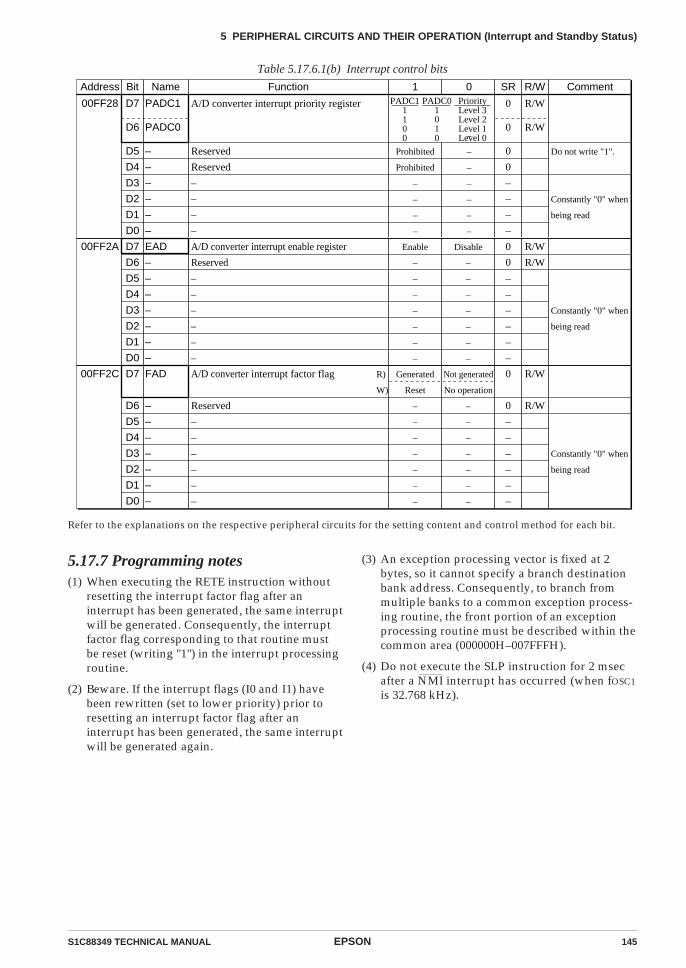
S1C88349 TECHNICAL MANUAL EPSON 145
5 PERIPHERAL CIRCUITS AND THEIR OPERATION (Interrupt and Standby Status)
Table 5.17.6.1(b) Interrupt control bits
Address Bit Name SR R/WFunction Comment1 0
00FF28 D7
D6
D5
D4
D3
D2
D1
D0
PADC1
PADC0
–
–
–
–
–
–
A/D converter interrupt priority register
Reserved
Reserved
–
–
–
–
Do not write "1".
Constantly "0" when
being read
0
0
0
0
–
–
–
–
R/W
R/W
Prohibited
Prohibited
–
–
–
–
–
–
–
–
–
–
–
PADC11100
PADC01010
PriorityLevel 3Level 2Level 1Level 0
00FF2A D7
D6
D5
D4
D3
D2
D1
D0
EAD
–
–
–
–
–
–
–
A/D converter interrupt enable register
Reserved
–
–
–
–
–
–
Constantly "0" when
being read
0
0
–
–
–
–
–
–
R/W
R/W
Enable
–
–
–
–
–
–
–
Disable
–
–
–
–
–
–
–
00FF2C D7
D6
D5
D4
D3
D2
D1
D0
FAD
–
–
–
–
–
–
–
A/D converter interrupt factor flag
Reserved
–
–
–
–
–
–
Constantly "0" when
being read
0
0
–
–
–
–
–
–
R/W
R/W
Generated
Reset
R)
W)
Not generated
No operation
–
–
–
–
–
–
–
–
–
–
–
–
–
–
Refer to the explanations on the respective peripheral circuits for the setting content and control method for each bit.
5.17.7 Programming notes(1) When executing the RETE instruction without
resetting the interrupt factor flag after aninterrupt has been generated, the same interruptwill be generated. Consequently, the interruptfactor flag corresponding to that routine mustbe reset (writing "1") in the interrupt processingroutine.
(2) Beware. If the interrupt flags (I0 and I1) havebeen rewritten (set to lower priority) prior toresetting an interrupt factor flag after aninterrupt has been generated, the same interruptwill be generated again.
(3) An exception processing vector is fixed at 2bytes, so it cannot specify a branch destinationbank address. Consequently, to branch frommultiple banks to a common exception process-ing routine, the front portion of an exceptionprocessing routine must be described within thecommon area (000000H–007FFFH).
(4) Do not execute the SLP instruction for 2 msecafter a NMI interrupt has occurred (when fOSC1
is 32.768 kHz).
146 EPSON S1C88349 TECHNICAL MANUAL
6 SUMMARY OF NOTES
6 SUMMARY OF NOTES6.1 Notes for Low Current
ConsumptionThe S1C88349 can turn circuits, which consume alarge amount of power, ON or OFF by controlregisters.You can reduce power consumption by creating aprogram that operates the minimum necessarycircuits using these control registers.
Next, which circuit systems' operation can becontrolled and their control registers (instructions)are explained. You should refer to these whenprogramming.
See Chapter 8, "ELECTRICAL CHARACTERIS-TICS" for the current consumption.
Refer to "Programming notes" in each peripheralsection for precautions of each peripheral circuit.
Table 6.1.1 Circuit systems and control registers
Circuit type
CPUOscillation circuit
Operating modeLCD controllerSVD circuitAnalog comparatorA/D converter
Status at time of initial resetting
Operation statusOSC1 clock (CLKCHG = "0")OSC3 oscillation OFF (OSCC = "0")Normal mode (VDC0 = VDC1 = "0")Drive OFF (LCDC0 = LCDC1 = "0")OFF status (SVDON = SVDSP = "0")OFF status (CMP0ON = CMP1ON = "0")OFF status (PRAD = ADRUN = "0")
Control register (Instruction)
HALT and SLP instructionsCLKCHG, OSCC
VDC0, VDC1LCDC0, LCDC1SVDON, SVDSP
CMP0ON, CMP1ONPRAD, ADRUN
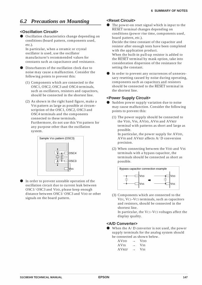
S1C88349 TECHNICAL MANUAL EPSON 147
6 SUMMARY OF NOTES
6.2 Precautions on Mounting
<Oscillation Circuit> Oscillation characteristics change depending on
conditions (board pattern, components used,etc.).In particular, when a ceramic or crystaloscillator is used, use the oscillatormanufacturer's recommended values forconstants such as capacitance and resistance.
Disturbances of the oscillation clock due tonoise may cause a malfunction. Consider thefollowing points to prevent this:
(1) Components which are connected to theOSC1, OSC2, OSC3 and OSC4 terminals,such as oscillators, resistors and capacitors,should be connected in the shortest line.
(2) As shown in the right hand figure, make aVSS pattern as large as possible at circum-scription of the OSC1, OSC2, OSC3 andOSC4 terminals and the componentsconnected to these terminals.Furthermore, do not use this VSS pattern forany purpose other than the oscillationsystem.
OSC4
OSC3
VSS
Sample VSS pattern (OSC3)
In order to prevent unstable operation of theoscillation circuit due to current leak betweenOSC1/OSC3 and VDD, please keep enoughdistance between OSC1/OSC3 and VDD or othersignals on the board pattern.
<Reset Circuit> The power-on reset signal which is input to the
RESET terminal changes depending onconditions (power rise time, components used,board pattern, etc.).Decide the time constant of the capacitor andresistor after enough tests have been completedwith the application product.When the built-in pull-up resistor is added tothe RESET terminal by mask option, take intoconsideration dispersion of the resistance forsetting the constant.
In order to prevent any occurrences of unneces-sary resetting caused by noise during operating,components such as capacitors and resistorsshould be connected to the RESET terminal inthe shortest line.
<Power Supply Circuit> Sudden power supply variation due to noise
may cause malfunction. Consider the followingpoints to prevent this:
(1) The power supply should be connected tothe VDD, VSS, AVDD, AVSS and AVREF
terminal with patterns as short and large aspossible.In particular, the power supply for AVDD,AVSS and AVREF affects A/D conversionprecision.
(2) When connecting between the VDD and VSS
terminals with a bypass capacitor, theterminals should be connected as short aspossible.
VDD
VSS
Bypass capacitor connection example
VDD
VSS
(3) Components which are connected to theVD1, VC1–VC5 terminals, such as capacitorsand resistors, should be connected in theshortest line.In particular, the VC1–VC5 voltages affect thedisplay quality.
<A/D Converter> When the A/D converter is not used, the power
supply terminals for the analog system shouldbe connected as shown below.
AVDD → VDD
AVSS → VSS
AVREF → VSS
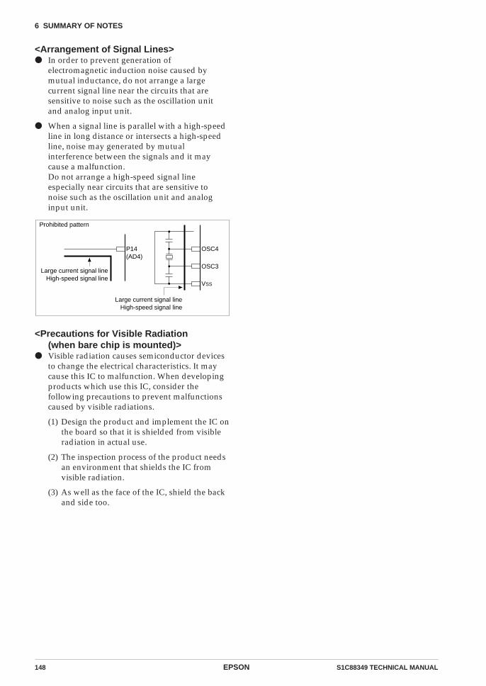
148 EPSON S1C88349 TECHNICAL MANUAL
6 SUMMARY OF NOTES
<Arrangement of Signal Lines> In order to prevent generation of
electromagnetic induction noise caused bymutual inductance, do not arrange a largecurrent signal line near the circuits that aresensitive to noise such as the oscillation unitand analog input unit.
When a signal line is parallel with a high-speedline in long distance or intersects a high-speedline, noise may generated by mutualinterference between the signals and it maycause a malfunction.Do not arrange a high-speed signal lineespecially near circuits that are sensitive tonoise such as the oscillation unit and analoginput unit.
P14 (AD4)
Large current signal lineHigh-speed signal line
OSC4
OSC3
VSS
Large current signal lineHigh-speed signal line
Prohibited pattern
<Precautions for Visible Radiation(when bare chip is mounted)>
Visible radiation causes semiconductor devicesto change the electrical characteristics. It maycause this IC to malfunction. When developingproducts which use this IC, consider thefollowing precautions to prevent malfunctionscaused by visible radiations.
(1) Design the product and implement the IC onthe board so that it is shielded from visibleradiation in actual use.
(2) The inspection process of the product needsan environment that shields the IC fromvisible radiation.
(3) As well as the face of the IC, shield the backand side too.
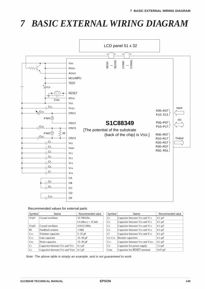
S1C88349 TECHNICAL MANUAL EPSON 149
7 BASIC EXTERNAL WIRING DIAGRAM
7 BASIC EXTERNAL WIRING DIAGRAM
Note: The above table is simply an example, and is not guaranteed to work.
[The potential of the substrate (back of the chip) is VSS.]
Symbol
X'tal1
X'tal2
Rf
CG1
CG2
CD2
C1
C2
Name
Crystal oscillator
Crystal oscillator
Feedback resistor
Trimmer capacitor
Gate capacitor
Drain capacitor
Capacitor between VSS and VD1
Capacitor between VSS and VREF
Recommended value
32.768 kHz,
CI (Max.) = 35 kΩ4.9152 MHz
1 MΩ5–25 pF
15–30 pF
15–30 pF
0.1 µF
0.1 µF
Recommended values for external parts
Symbol
C3
C4
C5
C6
C7
C8–C10
C11
CP
Cres
Name
Capacitor between VSS and VC1
Capacitor between VSS and VC2
Capacitor between VSS and VC3
Capacitor between VSS and VC4
Capacitor between VSS and VC5
Booster capacitors
Capacitor between VSS and VOSC
Capacitor for power supply
Capacitor for RESET terminal
Recommended value
0.1 µF
0.1 µF
0.1 µF
0.1 µF
0.1 µF
0.1 µF
0.1 µF
3.3 µF
0.47 µF
VDD
AVDD
AVREF
MCU/MPU
TEST
RESET
AVSS
VSS
VOSC
OSC1
OSC2
OSC3
OSC4
VD1
VREF
VC1
VC2
VC3
VC4
VC5
CA
CB
CC
CD
CE
K00–K07K10, K11
P00–P07P10–P17
R00–R07R10–R17R20–R27R30–R37R50, R51
S1C88349
SE
G0
|
SE
G50
CO
M0
|
CO
M31
LCD panel 51 x 32
C11
C1
C2
C3
C4
C5
C6
C7
C8
C9
C10
CG1
CG2
CD2
Cres
Rf
X'tal1
X'tal2
Output
I/O
Input
-+
CP
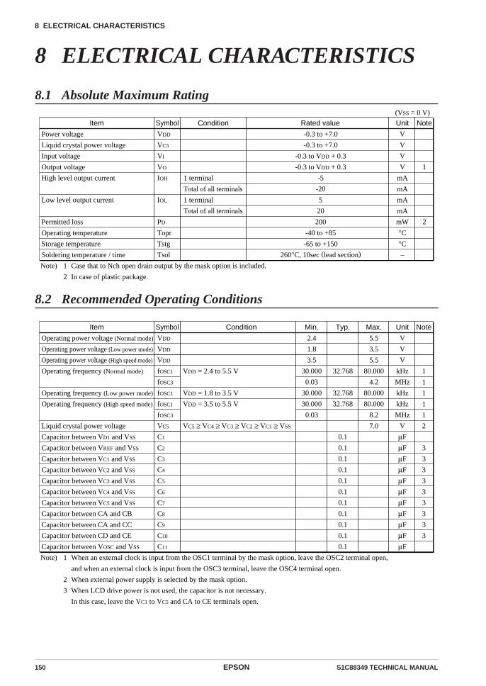
150 EPSON S1C88349 TECHNICAL MANUAL
8 ELECTRICAL CHARACTERISTICS
8 ELECTRICAL CHARACTERISTICS
8.1 Absolute Maximum Rating
Item Symbol UnitRated value
Power voltage
Liquid crystal power voltage
Input voltage
Output voltage
High level output current
Low level output current
Permitted loss
Operating temperature
Storage temperature
Soldering temperature / time
VDD
VC5
VI
VO
IOH
IOL
PD
Topr
Tstg
Tsol
V
V
V
V
mA
mA
mA
mA
mW
°C
°C
–
-0.3 to +7.0
-0.3 to +7.0
-0.3 to VDD + 0.3
-0.3 to VDD + 0.3
-5
-20
5
20
200
-40 to +85
-65 to +150
260°C, 10sec (lead section)
Note)
Note
1
2
Condition
1 terminal
Total of all terminals
1 terminal
Total of all terminals
1
2
Case that to Nch open drain output by the mask option is included.
In case of plastic package.
(VSS = 0 V)
8.2 Recommended Operating Conditions
Item Symbol Min. Typ. Max. UnitCondition
Operating power voltage (Normal mode)
Operating power voltage (Low power mode)
Operating power voltage (High speed mode)
Operating frequency (Normal mode)
Operating frequency (Low power mode)
Operating frequency (High speed mode)
Liquid crystal power voltage
Capacitor between VD1 and VSS
Capacitor between VREF and VSS
Capacitor between VC1 and VSS
Capacitor between VC2 and VSS
Capacitor between VC3 and VSS
Capacitor between VC4 and VSS
Capacitor between VC5 and VSS
Capacitor between CA and CB
Capacitor between CA and CC
Capacitor between CD and CE
Capacitor between VOSC and VSS
VDD
VDD
VDD
fOSC1
fOSC3
fOSC1
fOSC1
fOSC3
VC5
C1
C2
C3
C4
C5
C6
C7
C8
C9
C10
C11
2.4
1.8
3.5
30.000
0.03
30.000
30.000
0.03
32.768
32.768
32.768
0.1
0.1
0.1
0.1
0.1
0.1
0.1
0.1
0.1
0.1
0.1
5.5
3.5
5.5
80.000
4.2
80.000
80.000
8.2
7.0
V
V
V
kHz
MHz
kHz
kHz
MHz
V
µF
µF
µF
µF
µF
µF
µF
µF
µF
µF
µF
VDD = 2.4 to 5.5 V
VDD = 1.8 to 3.5 V
VDD = 3.5 to 5.5 V
VC5 ≥ VC4 ≥ VC3 ≥ VC2 ≥ VC1 ≥ VSS
Note
1
1
1
1
1
2
3
3
3
3
3
3
3
3
3
Note) 1
2
3
When an external clock is input from the OSC1 terminal by the mask option, leave the OSC2 terminal open,
and when an external clock is input from the OSC3 terminal, leave the OSC4 terminal open.
When external power supply is selected by the mask option.
When LCD drive power is not used, the capacitor is not necessary.
In this case, leave the VC1 to VC5 and CA to CE terminals open.
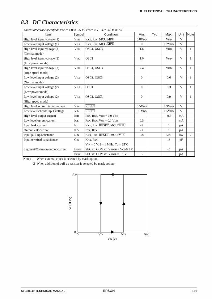
S1C88349 TECHNICAL MANUAL EPSON 151
8 ELECTRICAL CHARACTERISTICS
8.3 DC Characteristics
Item Symbol Min. Typ. Max. UnitCondition
High level input voltage (1)
Low level input voltage (1)
High level input voltage (2)
(Normal mode)
High level input voltage (2)
(Low power mode)
High level input voltage (2)
(High speed mode)
Low level input voltage (2)
(Normal mode)
Low level input voltage (2)
(Low power mode)
Low level input voltage (2)
(High speed mode)
High level schmitt input voltage
Low level schmitt input voltage
High level output current
Low level output current
Input leak current
Output leak current
Input pull-up resistance
Input terminal capacitance
Segment/Common output current
VIH1
VIL1
VIH2
VIH2
VIH2
VIL2
VIL2
VIL2
VT+
VT-
IOH
IOL
ILI
ILO
RIN
CIN
ISEGH
ISEGL
0.8VDD
0
1.6
1.0
2.4
0
0
0
0.5VDD
0.1VDD
0.5
-1
-1
100
5
VDD
0.2VDD
VDD
VDD
VDD
0.6
0.3
0.9
0.9VDD
0.5VDD
-0.5
1
1
500
15
-5
V
V
V
V
V
V
V
V
V
V
mA
mA
µA
µA
kΩpF
µA
µA
Kxx, Pxx, MCU/MPU
Kxx, Pxx, MCU/MPU
OSC1, OSC3
OSC1
OSC1, OSC3
OSC1, OSC3
OSC1
OSC1, OSC3
RESET
RESET
Pxx, Rxx, VOH = 0.9 VDD
Pxx, Rxx, VOL = 0.1 VDD
Kxx, Pxx, RESET, MCU/MPU
Pxx, Rxx
Kxx, Pxx, RESET, MCU/MPU
Kxx, Pxx
VIN = 0 V, f = 1 MHz, Ta = 25°C
SEGxx, COMxx, VSEGH = VC5-0.1 V
SEGxx, COMxx, VSEGL = 0.1 V
Note
1
1
1
1
1
1
2
Note) 1
2
When external clock is selected by mask option.
When addition of pull-up resistor is selected by mask option.
Unless otherwise specified: VDD = 1.8 to 5.5 V, VSS = 0 V, Ta = -40 to 85°C
VDD
0VT+VT-0
VIN (V)
VO
UT
(V
)
VDD
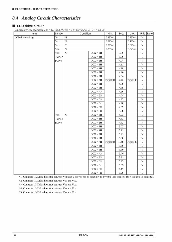
152 EPSON S1C88349 TECHNICAL MANUAL
8 ELECTRICAL CHARACTERISTICS
8.4 Analog Circuit Characteristics
LCD drive circuit
LCD drive voltage VC1
VC2
VC3
VC4
VC5
TYPE A
(4.5V)
VC5
TYPE B
(5.5V)
0.19VC5
0.39VC5
0.59VC5
0.78VC5
Typ×0.94
Typ×0.94
3.89
3.96
4.04
4.11
4.18
4.26
4.34
4.42
4.50
4.58
4.66
4.74
4.82
4.90
4.99
5.08
4.73
4.83
4.92
5.02
5.11
5.21
5.30
5.40
5.50
5.60
5.70
5.81
5.93
6.05
6.17
6.29
0.23VC5
0.43VC5
0.62VC5
0.82VC5
Typ×1.06
Typ×1.06
V
V
V
V
V
V
V
V
V
V
V
V
V
V
V
V
V
V
V
V
V
V
V
V
V
V
V
V
V
V
V
V
V
V
V
V
*1
*2
*3
*4
*5
*5
LCX = 0H
LCX = 1H
LCX = 2H
LCX = 3H
LCX = 4H
LCX = 5H
LCX = 6H
LCX = 7H
LCX = 8H
LCX = 9H
LCX = AH
LCX = BH
LCX = CH
LCX = DH
LCX = EH
LCX = FH
LCX = 0H
LCX = 1H
LCX = 2H
LCX = 3H
LCX = 4H
LCX = 5H
LCX = 6H
LCX = 7H
LCX = 8H
LCX = 9H
LCX = AH
LCX = BH
LCX = CH
LCX = DH
LCX = EH
LCX = FH
Item Symbol Min. Typ. Max. UnitCondition Note
*1
*2
*3
*4
*5
Unless otherwise specified: VDD = 1.8 to 5.5 V, VSS = 0 V, Ta = 25°C, C1–C11 = 0.1 µF
Connects 1 MΩ load resistor between VDD and VC1 (VC1 has no capability to drive the load connected to VSS due to its property).
Connects 1 MΩ load resistor between VSS and VC2.
Connects 1 MΩ load resistor between VSS and VC3.
Connects 1 MΩ load resistor between VSS and VC4.
Connects 1 MΩ load resistor between VSS and VC5.
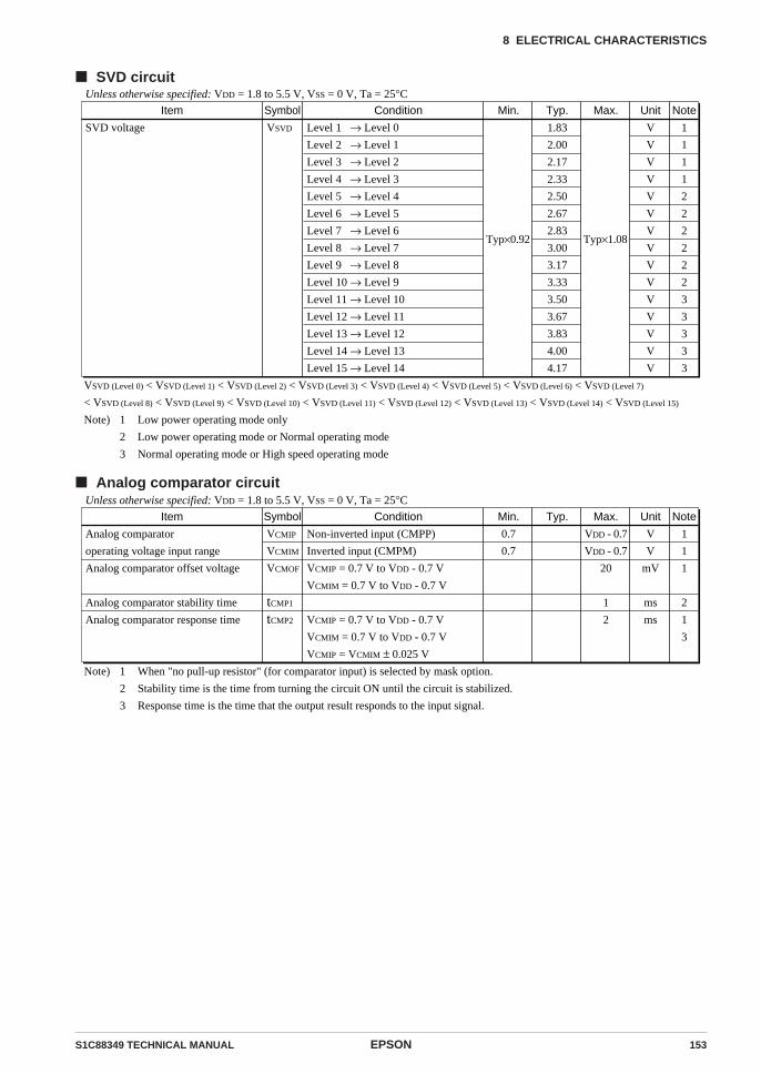
S1C88349 TECHNICAL MANUAL EPSON 153
8 ELECTRICAL CHARACTERISTICS
SVD circuit
Item Symbol Min. Typ. Max. UnitCondition
SVD voltage VSVD
Typ×0.92
1.83
2.00
2.17
2.33
2.50
2.67
2.83
3.00
3.17
3.33
3.50
3.67
3.83
4.00
4.17
Typ×1.08
V
V
V
V
V
V
V
V
V
V
V
V
V
V
V
Level 1 → Level 0
Level 2 → Level 1
Level 3 → Level 2
Level 4 → Level 3
Level 5 → Level 4
Level 6 → Level 5
Level 7 → Level 6
Level 8 → Level 7
Level 9 → Level 8
Level 10 → Level 9
Level 11 → Level 10
Level 12 → Level 11
Level 13 → Level 12
Level 14 → Level 13
Level 15 → Level 14
Note
1
1
1
1
2
2
2
2
2
2
3
3
3
3
3
VSVD (Level 0) < VSVD (Level 1) < VSVD (Level 2) < VSVD (Level 3) < VSVD (Level 4) < VSVD (Level 5) < VSVD (Level 6) < VSVD (Level 7)
< VSVD (Level 8) < VSVD (Level 9) < VSVD (Level 10) < VSVD (Level 11) < VSVD (Level 12) < VSVD (Level 13) < VSVD (Level 14) < VSVD (Level 15)
Unless otherwise specified: VDD = 1.8 to 5.5 V, VSS = 0 V, Ta = 25°C
Note) 1
2
3
Low power operating mode only
Low power operating mode or Normal operating mode
Normal operating mode or High speed operating mode
Analog comparator circuit
Item Symbol Min. Typ. Max. UnitCondition
Analog comparator
operating voltage input range
Analog comparator offset voltage
Analog comparator stability time
Analog comparator response time
VCMIP
VCMIM
VCMOF
tCMP1
tCMP2
0.7
0.7
VDD - 0.7
VDD - 0.7
20
1
2
V
V
mV
ms
ms
Non-inverted input (CMPP)
Inverted input (CMPM)
VCMIP = 0.7 V to VDD - 0.7 V
VCMIM = 0.7 V to VDD - 0.7 V
VCMIP = 0.7 V to VDD - 0.7 V
VCMIM = 0.7 V to VDD - 0.7 V
VCMIP = VCMIM ± 0.025 V
Note
1
1
1
2
1
3
Note) 1
2
3
When "no pull-up resistor" (for comparator input) is selected by mask option.
Stability time is the time from turning the circuit ON until the circuit is stabilized.
Response time is the time that the output result responds to the input signal.
Unless otherwise specified: VDD = 1.8 to 5.5 V, VSS = 0 V, Ta = 25°C

154 EPSON S1C88349 TECHNICAL MANUAL
8 ELECTRICAL CHARACTERISTICS
A/D converter circuit
Item Symbol Min. Typ. Max. UnitCondition
Zero-scale error
Full-scale error
Non-linearity error
Total error
A/D converter
current consumption
A/D conversion clock
Ezs
Efs
El
Et
IAD
f
-1.5
-1.5
-5
-5
0.03
70
250
+1.5
+1.5
+5
+5
130
350
1
LSB
LSB
LSB
LSB
µA
µA
MHz
VDD = AVDD = AVREF = 2.4 to 5.5 V,
ADCLK = 1 MHz, Ta = 25°C
VDD = AVDD = AVREF = 3.0 V,
ADCLK = 1 MHz, Ta = 25°C
AVREF and ADCLK divider current
not included
VDD = AVDD = AVREF = 5.0 V,
ADCLK = 1 MHz, Ta = 25°C
AVREF and ADCLK divider current
not included
VDD = AVDD = AVREF = 2.4 to 5.5 V,
Ta = 25°C
Note
1
1
2
Note) 1
2
Average current during conversion
See Table 5.15.4.2 in "5.15 A/D Converter" for setting the A/D conversion clock.
Unless otherwise specified: VDD = AVDD = AVREF = 5.0 V, VSS = AVSS =0 V, fOSC1 = 32.768 kHz, fOSC3 = 4.0 MHz, Ta = 25°C
∗ Zero-scale error: Ezs = deviation from the ideal value at zero point
∗ Full-scale error: Efs = deviation from the ideal value at the full scale point
∗ Non-linearity error: El = deviation of the real conversion curve from the end point line
∗ Total error: Et = max (Ezs, Efs, Eabs), Eabs = deviation from the ideal line (including quantization error)
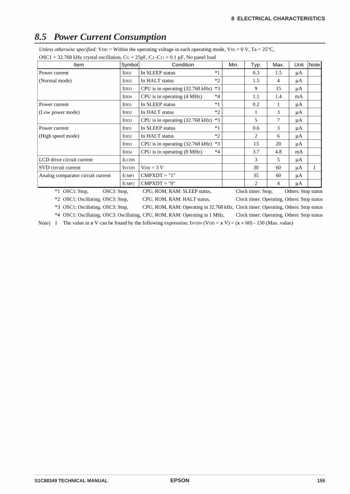
S1C88349 TECHNICAL MANUAL EPSON 155
8 ELECTRICAL CHARACTERISTICS
8.5 Power Current Consumption
Item Symbol Min. Typ. Max. UnitCondition
Power current
(Normal mode)
Power current
(Low power mode)
Power current
(High speed mode)
LCD drive circuit current
SVD circuit current
Analog comparator circuit current
IDD1
IDD2
IDD3
IDD4
IDD1
IDD2
IDD3
IDD1
IDD2
IDD3
IDD4
ILCDN
ISVDN
ICMP1
ICMP2
0.3
1.5
9
1.1
0.2
1
5
0.6
2
13
3.7
3
30
35
2
1.5
4
15
1.4
1
3
7
3
6
20
4.8
5
60
60
4
µA
µA
µA
mA
µA
µA
µA
µA
µA
µA
mA
µA
µA
µA
µA
In SLEEP status
In HALT status
CPU is in operating (32.768 kHz)
CPU is in operating (4 MHz)
In SLEEP status
In HALT status
CPU is in operating (32.768 kHz)
In SLEEP status
In HALT status
CPU is in operating (32.768 kHz)
CPU is in operating (8 MHz)
VDD = 3 V
CMPXDT = "1"
CMPXDT = "0"
Note
1
*1
*2
*3
*4
1
Unless otherwise specified: VDD = Within the operating voltage in each operating mode, VSS = 0 V, Ta = 25°C,
OSC1 = 32.768 kHz crystal oscillation, CG = 25pF, C1–C11 = 0.1 µF, No panel load
OSC1: Stop,
OSC1: Oscillating,
OSC1: Oscillating,
OSC1: Oscillating,
The value in x V can be found by the following expression: ISVDN (VDD = x V) = (x × 60) - 150 (Max. value)
*1
*2
*3
*4
*1
*2
*3
*1
*2
*3
*4
Note)
OSC3: Stop,
OSC3: Stop,
OSC3: Stop,
OSC3: Oscillating,
CPU, ROM, RAM: SLEEP status,
CPU, ROM, RAM: HALT status,
CPU, ROM, RAM: Operating in 32.768 kHz,
CPU, ROM, RAM: Operating in 1 MHz,
Clock timer: Stop,
Clock timer: Operating,
Clock timer: Operating,
Clock timer: Operating,
Others: Stop status
Others: Stop status
Others: Stop status
Others: Stop status
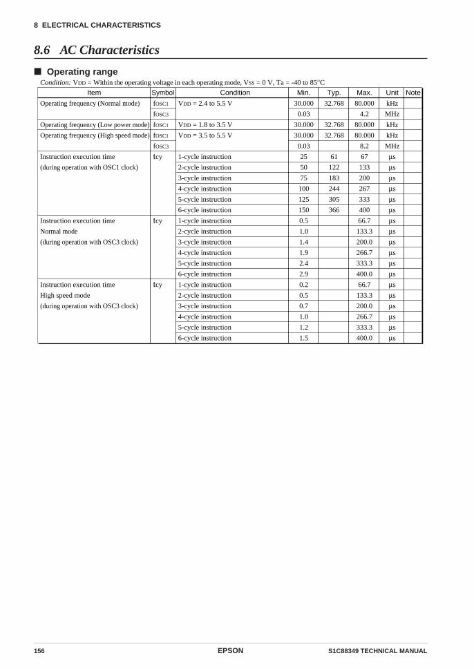
156 EPSON S1C88349 TECHNICAL MANUAL
8 ELECTRICAL CHARACTERISTICS
8.6 AC Characteristics
Operating rangeCondition: VDD = Within the operating voltage in each operating mode, VSS = 0 V, Ta = -40 to 85°C
Item Symbol Min. Typ. Max. UnitCondition
Operating frequency (Normal mode)
Operating frequency (Low power mode)
Operating frequency (High speed mode)
Instruction execution time
(during operation with OSC1 clock)
Instruction execution time
Normal mode
(during operation with OSC3 clock)
Instruction execution time
High speed mode
(during operation with OSC3 clock)
fOSC1
fOSC3
fOSC1
fOSC1
fOSC3
tcy
tcy
tcy
30.000
0.03
30.000
30.000
0.03
25
50
75
100
125
150
0.5
1.0
1.4
1.9
2.4
2.9
0.2
0.5
0.7
1.0
1.2
1.5
32.768
32.768
32.768
61
122
183
244
305
366
80.000
4.2
80.000
80.000
8.2
67
133
200
267
333
400
66.7
133.3
200.0
266.7
333.3
400.0
66.7
133.3
200.0
266.7
333.3
400.0
kHz
MHz
kHz
kHz
MHz
µs
µs
µs
µs
µs
µs
µs
µs
µs
µs
µs
µs
µs
µs
µs
µs
µs
µs
VDD = 2.4 to 5.5 V
VDD = 1.8 to 3.5 V
VDD = 3.5 to 5.5 V
1-cycle instruction
2-cycle instruction
3-cycle instruction
4-cycle instruction
5-cycle instruction
6-cycle instruction
1-cycle instruction
2-cycle instruction
3-cycle instruction
4-cycle instruction
5-cycle instruction
6-cycle instruction
1-cycle instruction
2-cycle instruction
3-cycle instruction
4-cycle instruction
5-cycle instruction
6-cycle instruction
Note
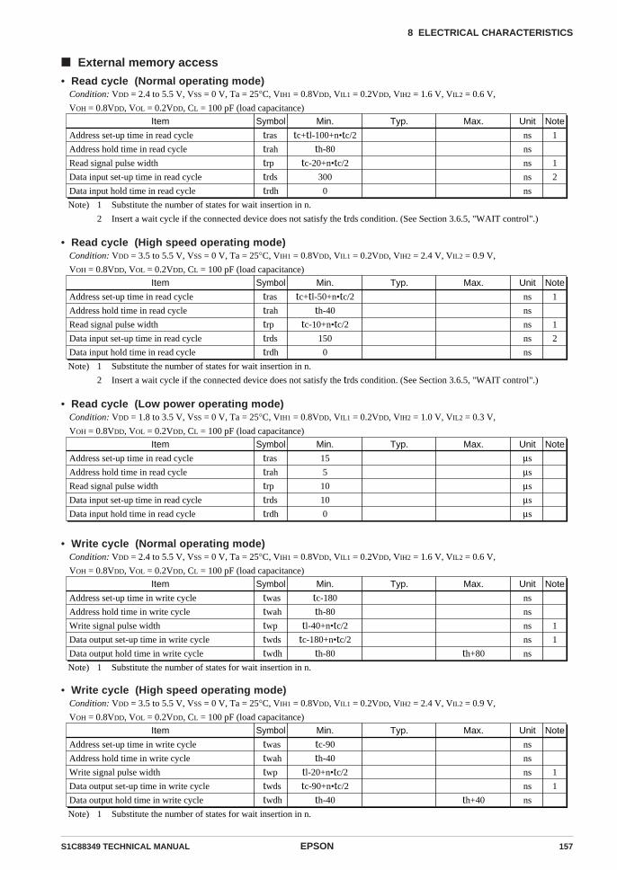
S1C88349 TECHNICAL MANUAL EPSON 157
8 ELECTRICAL CHARACTERISTICS
External memory access
• Read cycle (Normal operating mode)
Item Symbol Min. Typ. Max. Unit
Address set-up time in read cycle
Address hold time in read cycle
Read signal pulse width
Data input set-up time in read cycle
Data input hold time in read cycle
tras
trah
trptrds
trdh
ns
ns
ns
ns
ns
Note
1
1
2
Note) 1
2
Condition: VDD = 2.4 to 5.5 V, VSS = 0 V, Ta = 25°C, VIH1 = 0.8VDD, VIL1 = 0.2VDD, VIH2 = 1.6 V, VIL2 = 0.6 V,
VOH = 0.8VDD, VOL = 0.2VDD, CL = 100 pF (load capacitance)
Substitute the number of states for wait insertion in n.
Insert a wait cycle if the connected device does not satisfy the trds condition. (See Section 3.6.5, "WAIT control".)
tc+tl-100+n•tc/2
th-80
tc-20+n•tc/2
300
0
• Read cycle (High speed operating mode)
Item Symbol Min. Typ. Max. Unit
Address set-up time in read cycle
Address hold time in read cycle
Read signal pulse width
Data input set-up time in read cycle
Data input hold time in read cycle
tras
trah
trptrds
trdh
ns
ns
ns
ns
ns
Note
1
1
2
Note) 1
2
Condition: VDD = 3.5 to 5.5 V, VSS = 0 V, Ta = 25°C, VIH1 = 0.8VDD, VIL1 = 0.2VDD, VIH2 = 2.4 V, VIL2 = 0.9 V,
VOH = 0.8VDD, VOL = 0.2VDD, CL = 100 pF (load capacitance)
Substitute the number of states for wait insertion in n.
Insert a wait cycle if the connected device does not satisfy the trds condition. (See Section 3.6.5, "WAIT control".)
tc+tl-50+n•tc/2
th-40
tc-10+n•tc/2
150
0
• Read cycle (Low power operating mode)
Item Symbol Min. Typ. Max. Unit
Address set-up time in read cycle
Address hold time in read cycle
Read signal pulse width
Data input set-up time in read cycle
Data input hold time in read cycle
tras
trah
trptrds
trdh
µs
µs
µs
µs
µs
Note
Condition: VDD = 1.8 to 3.5 V, VSS = 0 V, Ta = 25°C, VIH1 = 0.8VDD, VIL1 = 0.2VDD, VIH2 = 1.0 V, VIL2 = 0.3 V,
VOH = 0.8VDD, VOL = 0.2VDD, CL = 100 pF (load capacitance)
15
5
10
10
0
• Write cycle (Normal operating mode)
Item Symbol Min. Typ. Max. Unit
Address set-up time in write cycle
Address hold time in write cycle
Write signal pulse width
Data output set-up time in write cycle
Data output hold time in write cycle
twas
twah
twp
twds
twdh
ns
ns
ns
ns
ns
Note
1
1
Note) 1
Condition: VDD = 2.4 to 5.5 V, VSS = 0 V, Ta = 25°C, VIH1 = 0.8VDD, VIL1 = 0.2VDD, VIH2 = 1.6 V, VIL2 = 0.6 V,
VOH = 0.8VDD, VOL = 0.2VDD, CL = 100 pF (load capacitance)
Substitute the number of states for wait insertion in n.
tc-180
th-80
tl-40+n•tc/2
tc-180+n•tc/2
th-80 th+80
• Write cycle (High speed operating mode)
Item Symbol Min. Typ. Max. Unit
Address set-up time in write cycle
Address hold time in write cycle
Write signal pulse width
Data output set-up time in write cycle
Data output hold time in write cycle
twas
twah
twp
twds
twdh
ns
ns
ns
ns
ns
Note
1
1
Note) 1
Condition: VDD = 3.5 to 5.5 V, VSS = 0 V, Ta = 25°C, VIH1 = 0.8VDD, VIL1 = 0.2VDD, VIH2 = 2.4 V, VIL2 = 0.9 V,
VOH = 0.8VDD, VOL = 0.2VDD, CL = 100 pF (load capacitance)
Substitute the number of states for wait insertion in n.
tc-90
th-40
tl-20+n•tc/2
tc-90+n•tc/2
th-40 th+40

158 EPSON S1C88349 TECHNICAL MANUAL
8 ELECTRICAL CHARACTERISTICS
• Write cycle (Low power operating mode)
Item Symbol Min. Typ. Max. Unit
Address set-up time in write cycle
Address hold time in write cycle
Write signal pulse width
Data output set-up time in write cycle
Data output hold time in write cycle
twas
twah
twp
twds
twdh
µs
µs
µs
µs
µs
Note
Condition: VDD = 1.8 to 3.5 V, VSS = 0 V, Ta = 25°C, VIH1 = 0.8VDD, VIL1 = 0.2VDD, VIH2 = 1.0 V, VIL2 = 0.3 V,
VOH = 0.8VDD, VOL = 0.2VDD, CL = 100 pF (load capacitance)
10
5
5
10
5 20
ICLK
A00–A18CE
RD
DIN
VIH2
VIL2
tc
th tl
VOHVOL
VOHVOL
tras trah
trdhtrdsVIH1
VIL1
trp
*
* *
A00–A18CE
WR
DOUT
VOHVOL
VOHVOL
twas twah
twdhtwdsVIH1
VIL1
twp
* In the case of crystal oscillation and ceramic oscillation: th = 0.5tc ± 0.05tc, tl = tc - th (1/tc: oscillation frequency)
* In the case of CR oscillation: th = 0.5tc ± 0.10tc, tl = tc - th (1/tc: oscillation frequency)

S1C88349 TECHNICAL MANUAL EPSON 159
8 ELECTRICAL CHARACTERISTICS
Serial interface
• Clock synchronous master mode (Normal operating mode)
Item Symbol Min. Typ. Max. Unit
Transmitting data output delay time
Receiving data input set-up time
Receiving data input hold time
tsmd
tsms
tsmh
ns
ns
ns
Note
500
200
200
Condition: VDD = 2.4 to 5.5 V, VSS = 0 V, Ta = 25°C, VIH1 = 0.8VDD, VIL1 = 0.2VDD, VOH = 0.8VDD, VOL = 0.2VDD
• Clock synchronous master mode (High speed operating mode)
Item Symbol Min. Typ. Max. Unit
Transmitting data output delay time
Receiving data input set-up time
Receiving data input hold time
tsmd
tsms
tsmh
ns
ns
ns
Note
250
100
100
Condition: VDD = 3.5 to 5.5 V, VSS = 0 V, Ta = 25°C, VIH1 = 0.8VDD, VIL1 = 0.2VDD, VOH = 0.8VDD, VOL = 0.2VDD
• Clock synchronous master mode (Low power operating mode)
Item Symbol Min. Typ. Max. Unit
Transmitting data output delay time
Receiving data input set-up time
Receiving data input hold time
tsmd
tsms
tsmh
µs
µs
µs
Note
10
5
5
Condition: VDD = 1.8 to 3.5 V, VSS = 0 V, Ta = 25°C, VIH1 = 0.8VDD, VIL1 = 0.2VDD, VOH = 0.8VDD, VOL = 0.2VDD
• Clock synchronous slave mode (Normal operating mode)
Item Symbol Min. Typ. Max. Unit
Transmitting data output delay time
Receiving data input set-up time
Receiving data input hold time
tssd
tsss
tssh
ns
ns
ns
Note
200
200
500
Condition: VDD = 2.4 to 5.5 V, VSS = 0 V, Ta = 25°C, VIH1 = 0.8VDD, VIL1 = 0.2VDD, VOH = 0.8VDD, VOL = 0.2VDD
• Clock synchronous slave mode (High speed operating mode)
Item Symbol Min. Typ. Max. Unit
Transmitting data output delay time
Receiving data input set-up time
Receiving data input hold time
tssd
tsss
tssh
ns
ns
ns
Note
100
100
250
Condition: VDD = 3.5 to 5.5 V, VSS = 0 V, Ta = 25°C, VIH1 = 0.8VDD, VIL1 = 0.2VDD, VOH = 0.8VDD, VOL = 0.2VDD
• Clock synchronous slave mode (Low power operating mode)
Item Symbol Min. Typ. Max. Unit
Transmitting data output delay time
Receiving data input set-up time
Receiving data input hold time
tssd
tsss
tssh
µs
µs
µs
Note
5
5
10
Condition: VDD = 1.8 to 3.5 V, VSS = 0 V, Ta = 25°C, VIH1 = 0.8VDD, VIL1 = 0.2VDD, VOH = 0.8VDD, VOL = 0.2VDD
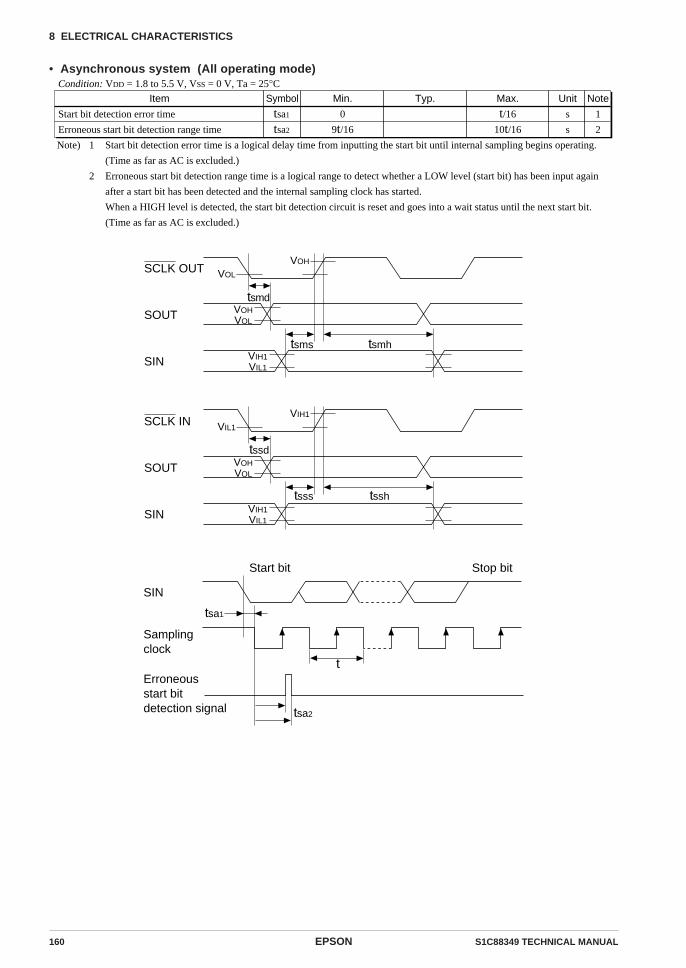
160 EPSON S1C88349 TECHNICAL MANUAL
8 ELECTRICAL CHARACTERISTICS
• Asynchronous system (All operating mode)
Min. Typ. Max.
tsa1
tsa2
s
s
1
2
Note) 1
2
Start bit detection error time is a logical delay time from inputting the start bit until internal sampling begins operating.
(Time as far as AC is excluded.)
Erroneous start bit detection range time is a logical range to detect whether a LOW level (start bit) has been input again
after a start bit has been detected and the internal sampling clock has started.
When a HIGH level is detected, the start bit detection circuit is reset and goes into a wait status until the next start bit.
(Time as far as AC is excluded.)
0
9t/16
t/16
10t/16
Item Symbol Unit
Start bit detection error time
Erroneous start bit detection range time
NoteCondition: VDD = 1.8 to 5.5 V, VSS = 0 V, Ta = 25°C
SCLK OUT
SOUT
SIN
VOH
VOHVOL
tsms tsmh
tsmd
VIH1VIL1
VOL
SCLK IN
SOUT
SIN
VIH1
VOHVOL
tsss tssh
tssd
VIH1VIL1
VIL1
tsa1
t
tsa2
SIN
Start bit
Samplingclock
Erroneous start bit detection signal
Stop bit

S1C88349 TECHNICAL MANUAL EPSON 161
8 ELECTRICAL CHARACTERISTICS
Input clock
• OSC1, OSC3 external clock (Normal operating mode)
Item Symbol Min. Typ. Max. Unit
OSC1 input clock time
OSC3 input clock time
Input clock rising time
Input clock falling time
to1cy
to1h
to1l
to3cy
to3h
to3l
tosr
tosf
µs
µs
µs
ns
ns
ns
ns
ns
Note
20
10
10
250
125
125
32
16
16
32,000
16,000
16,000
25
25
Cycle time
"H" pulse width
"L" pulse width
Cycle time
"H" pulse width
"L" pulse width
Condition: VDD = 2.4 to 5.5 V, VSS = 0 V, Ta = -40 to 85°C, VIH2 = 1.6 V, VIL2 = 0.6 V
• OSC1, OSC3 external clock (High speed operating mode)
Item Symbol Min. Typ. Max. Unit
OSC1 input clock time
OSC3 input clock time
Input clock rising time
Input clock falling time
to1cy
to1h
to1l
to3cy
to3h
to3l
tosr
tosf
µs
µs
µs
ns
ns
ns
ns
ns
Note
20
10
10
125
62.5
62.5
32
16
16
32,000
16,000
16,000
25
25
Cycle time
"H" pulse width
"L" pulse width
Cycle time
"H" pulse width
"L" pulse width
Condition: VDD = 3.5 to 5.5 V, VSS = 0 V, Ta = -40 to 85°C, VIH2 = 2.4 V, VIL2 = 0.9 V
• OSC1, OSC3 external clock (Low power operating mode)
Item Symbol Min. Typ. Max. Unit
OSC1 input clock time
Input clock rising time
Input clock falling time
to1cy
to1h
to1l
tosr
tosf
µs
µs
µs
ns
ns
Note
20
10
10
32
16
16
25
25
Cycle time
"H" pulse width
"L" pulse width
Condition: VDD = 1.8 to 3.5 V, VSS = 0 V, Ta = -40 to 85°C, VIH2 = 1.0 V, VIL2 = 0.3 V
OSC1
OSC3
VIH2
to1cy
to1h
VIL2
tosf tosr
to1l
VIH2
to3cy
to3h
VIL2
tosf tosr
to3l
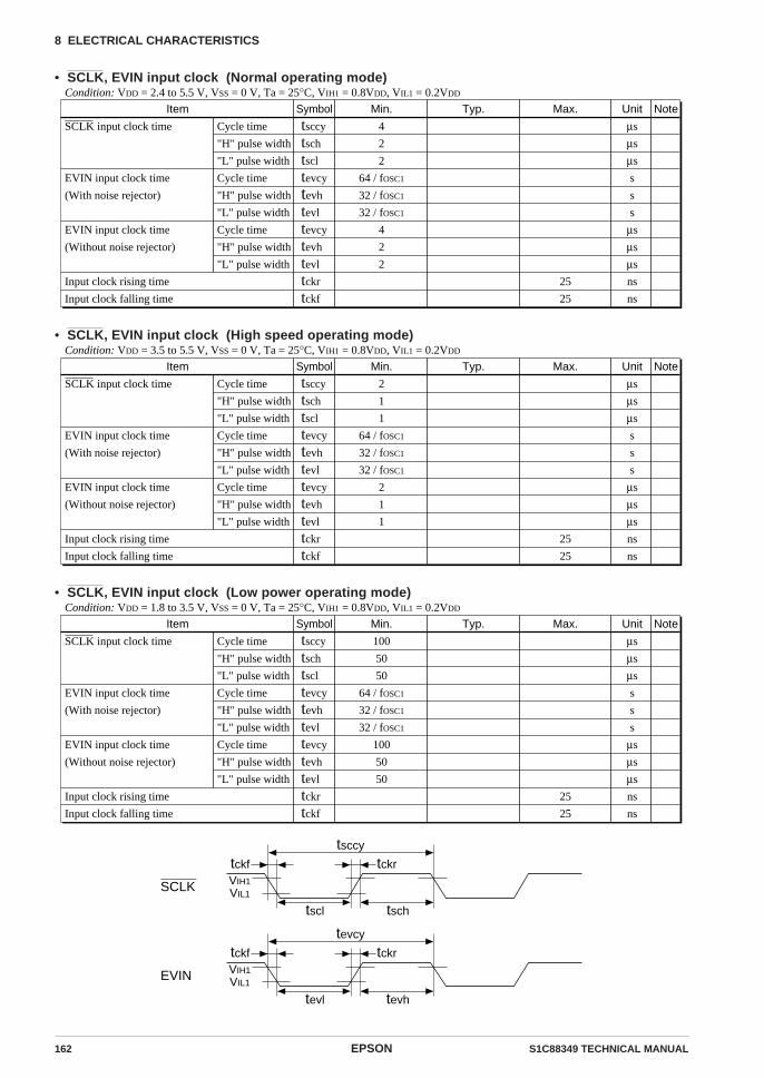
162 EPSON S1C88349 TECHNICAL MANUAL
8 ELECTRICAL CHARACTERISTICS
• SCLK, EVIN input clock (Normal operating mode)
Item Symbol Min. Typ. Max. Unit
SCLK input clock time
EVIN input clock time
(With noise rejector)
EVIN input clock time
(Without noise rejector)
Input clock rising time
Input clock falling time
tsccy
tsch
tscl
tevcy
tevh
tevl
tevcy
tevh
tevl
tckr
tckf
µs
µs
µs
s
s
s
µs
µs
µs
ns
ns
Note
4
2
2
64 / fOSC1
32 / fOSC1
32 / fOSC1
4
2
2
25
25
Cycle time
"H" pulse width
"L" pulse width
Cycle time
"H" pulse width
"L" pulse width
Cycle time
"H" pulse width
"L" pulse width
Condition: VDD = 2.4 to 5.5 V, VSS = 0 V, Ta = 25°C, VIH1 = 0.8VDD, VIL1 = 0.2VDD
• SCLK, EVIN input clock (High speed operating mode)
Item Symbol Min. Typ. Max. Unit
SCLK input clock time
EVIN input clock time
(With noise rejector)
EVIN input clock time
(Without noise rejector)
Input clock rising time
Input clock falling time
tsccy
tsch
tscl
tevcy
tevh
tevl
tevcy
tevh
tevl
tckr
tckf
µs
µs
µs
s
s
s
µs
µs
µs
ns
ns
Note
2
1
1
64 / fOSC1
32 / fOSC1
32 / fOSC1
2
1
1
25
25
Cycle time
"H" pulse width
"L" pulse width
Cycle time
"H" pulse width
"L" pulse width
Cycle time
"H" pulse width
"L" pulse width
Condition: VDD = 3.5 to 5.5 V, VSS = 0 V, Ta = 25°C, VIH1 = 0.8VDD, VIL1 = 0.2VDD
• SCLK, EVIN input clock (Low power operating mode)
Item Symbol Min. Typ. Max. Unit
SCLK input clock time
EVIN input clock time
(With noise rejector)
EVIN input clock time
(Without noise rejector)
Input clock rising time
Input clock falling time
tsccy
tsch
tscl
tevcy
tevh
tevl
tevcy
tevh
tevl
tckr
tckf
µs
µs
µs
s
s
s
µs
µs
µs
ns
ns
Note
100
50
50
64 / fOSC1
32 / fOSC1
32 / fOSC1
100
50
50
25
25
Cycle time
"H" pulse width
"L" pulse width
Cycle time
"H" pulse width
"L" pulse width
Cycle time
"H" pulse width
"L" pulse width
Condition: VDD = 1.8 to 3.5 V, VSS = 0 V, Ta = 25°C, VIH1 = 0.8VDD, VIL1 = 0.2VDD
SCLK
EVIN
VIH1
tsccy
tsch
VIL1
tckf tckr
tscl
VIH1
tevcy
tevh
VIL1
tckf tckr
tevl
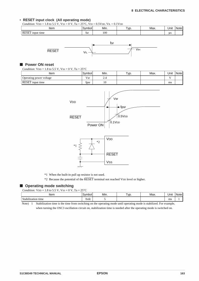
S1C88349 TECHNICAL MANUAL EPSON 163
8 ELECTRICAL CHARACTERISTICS
• RESET input clock (All operating mode)
Symbol Min. Typ. Max. Unit
RESET input time tsr µs
Note
100
ItemCondition: VDD = 1.8 to 5.5 V, VSS = 0 V, Ta = 25°C, VIH = 0.5VDD, VIL = 0.1VDD
RESET
tsr
VILVIH
Power ON reset
Symbol Min. Typ. Max. Unit
Operating power voltage
RESET input time
Vsr
tpsr
V
ms
Note
2.4
10
ItemCondition: VDD = 1.8 to 5.5 V, VSS = 0 V, Ta = 25°C
VDD
RESET
tpsr
Vsr
0.5VDD
0.1VDDPower ON
*1 When the built-in pull up resistor is not used.
*2 Because the potential of the RESET terminal not reached VDD level or higher.
VDD
RESET
VSS
*2*1
Operating mode switching
Symbol Min. Typ. Max. Unit
Stabilization time tvdc ms
Note
15
ItemCondition: VDD = 1.8 to 5.5 V, VSS = 0 V, Ta = 25°C
Note) 1 Stabilization time is the time from switching on the operating mode until operating mode is stabilized. For example,
when turning the OSC3 oscillation circuit on, stabilization time is needed after the operating mode is switched on.

164 EPSON S1C88349 TECHNICAL MANUAL
8 ELECTRICAL CHARACTERISTICS
8.7 Oscillation CharacteristicsOscillation characteristics change depending on conditions (board pattern, components used, etc.). Use thefollowing characteristics as reference values. In particular, when a ceramic oscillator is used for OSC3, usethe oscillator manufacturer’s recommended values for constants such as capacitance and resistance. Theoscillation start time is important because it becomes the wait time when OSC3 clock is used. (If OSC3 isused as CPU clock before oscillation stabilizes, the CPU may malfunction.)
OSC1 (Crystal)
Item Symbol Min. Typ. Max. UnitCondition
Oscillation start time
External gate capacitance
Built-in gate capacitance
Built-in drain capacitance
Frequency/IC deviation
Frequency/power voltage deviation
Frequency adjustment range
tsta
CG1
CG1
CD1
∂f/∂IC
∂f/∂V
∂f/∂CG
5
-10
25
17
10
3
25
10
1
s
pF
pF
pF
ppm
ppm/V
ppm
Including board capacitance
In case of the chip
In case of the chip
VDD = constant
VDD = constant, CG = 5 to 25pF
Note
1
2
Unless otherwise specified: VDD = Within the operating voltage in each operating mode, VSS = 0 V, Ta = 25°C,
Crystal oscillator = Q12C2*, CG1 = 25 pF, CD1 = Built-in
* Q12C2 Made by Seiko Epson corporationNote) 1
2
When crystal oscillation is selected by the mask option.
When crystal oscillation (gate capacitor built-in) is selected by the mask option.
OSC1 (CR)
Min. Typ. Max.
tsta
∂f/∂IC -25
100
25
µs
%RCR = constant
Oscillation start time
Frequency/IC deviation
Item Symbol UnitCondition NoteUnless otherwise specified: VDD = 2.4 to 5.5 V, VSS = 0 V, Ta = 25°C
OSC3 (Crystal)
Min. Typ. Max.
Oscillation start time (Normal mode)
Oscillation start time (High speed mode)
tsta
tsta
10
10
ms
ms
4.0 MHz crystal oscillator
8.0 MHz crystal oscillator
1
1
Item Symbol UnitCondition Note
Unless otherwise specified: VDD = Within the operating voltage in each operating mode, VSS = 0 V, Ta = 25°C,
Crystal oscillator = Q21CA301xxx*, RF = 1MΩ, CG2 = CD2 = 15pF
Note) 1 The crystal oscillation start time changes by the crystal oscillator to be used, CG2 and CD2.* Q21CA301xxx Made by Seiko Epson corporation
OSC3 (Ceramic)
Min. Typ. Max.
tsta
tsta
1
1
ms
ms
1
1
Oscillation start time (Normal mode)
Oscillation start time (High speed mode)
4.0 MHz ceramic oscillator
8.0 MHz ceramic oscillator
Item Symbol UnitCondition Note
Unless otherwise specified: VDD = Within the operating voltage in each operating mode, VSS = 0 V, Ta = 25°C,
Ceramic oscillator = CSA4.00MG / CSA8.00MTZ*, RF = 1MΩ, CG2 = CD2 = 30pF
*
1Note)
CSA4.00MG / CSA8.00MTZ Made by Murata Mfg. corporation
The ceramic oscillation start time changes by the ceramic oscillator to be used, CG2 and CD2.
OSC3 (CR)
Min. Typ. Max.
tsta
tsta
∂f/∂IC
∂f/∂IC
-25
-25
100
100
25
25
µs
µs
%
%
RCR = constant
RCR = constant
Oscillation start time (Normal mode)
Oscillation start time (High speed mode)
Frequency/IC deviation (Normal mode)
Frequency/IC deviation (High speed mode)
Item Symbol UnitCondition NoteUnless otherwise specified: VDD = Within the operating voltage in each operating mode, VSS = 0 V, Ta = 25°C
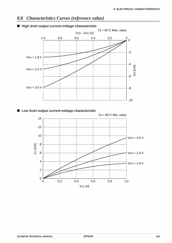
S1C88349 TECHNICAL MANUAL EPSON 165
8 ELECTRICAL CHARACTERISTICS
8.8 Characteristics Curves (reference value)
High level output current-voltage characteristic
1.0
VDD = 1.8 V
VDD = 2.4 V
VDD = 3.5 V
0.8 0.6 0.4
VDD - VOH [V]
IOH
[mA
]
0.2 00
-2
-4
-6
-8
-10
Ta = 85°C Max. value
Low level output current-voltage characteristic
0
VDD = 1.8 V
VDD = 2.4 V
VDD = 3.5 V
0.2 0.4 0.6
VOL [V]
IOL
[mA
]
0.8 1.0
14
12
10
8
6
4
2
0
Ta = 85°C Min. value
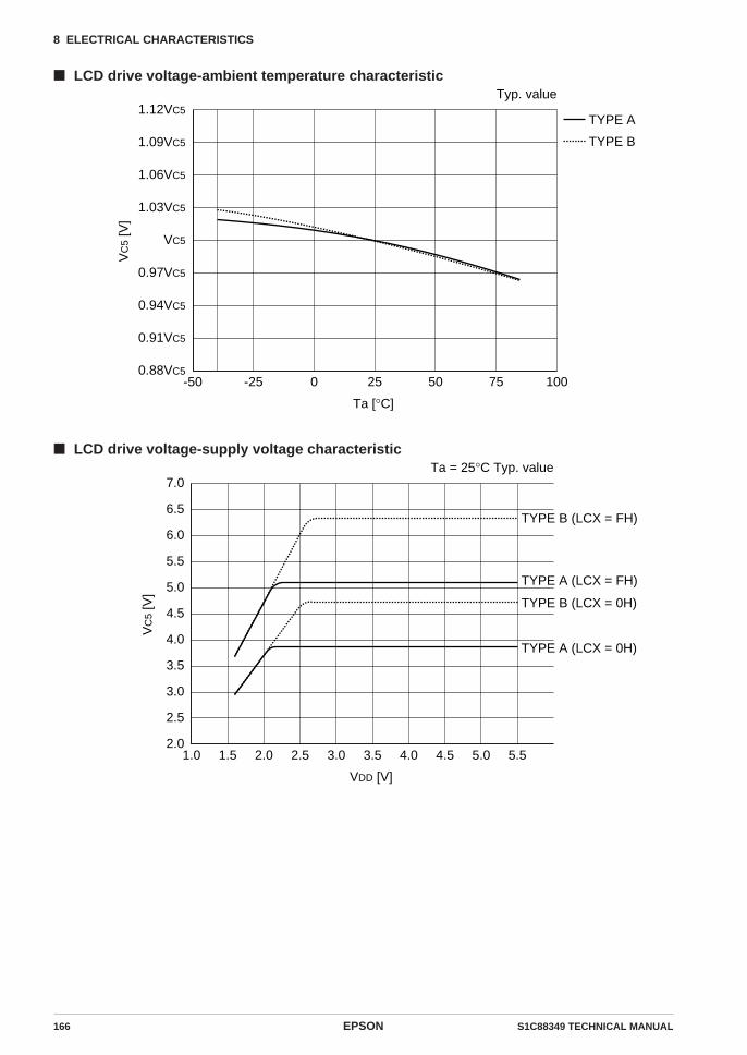
166 EPSON S1C88349 TECHNICAL MANUAL
8 ELECTRICAL CHARACTERISTICS
LCD drive voltage-ambient temperature characteristic
-50 -25 0 25 50 75 100
Ta [°C]
VC
5 [V
]1.12VC5
1.09VC5
1.06VC5
1.03VC5
VC5
0.97VC5
0.94VC5
0.91VC5
0.88VC5
Typ. value
TYPE A
TYPE B
LCD drive voltage-supply voltage characteristic
1.0 1.5 2.0 2.5 3.0 3.5 4.0 4.5 5.0 5.5
VDD [V]
TYPE B (LCX = FH)
TYPE A (LCX = FH)
TYPE B (LCX = 0H)
TYPE A (LCX = 0H)
VC
5 [V
]
7.0
6.5
6.0
5.5
5.0
4.5
4.0
3.5
3.0
2.5
2.0
Ta = 25°C Typ. value
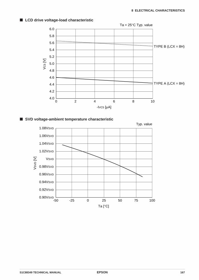
S1C88349 TECHNICAL MANUAL EPSON 167
8 ELECTRICAL CHARACTERISTICS
LCD drive voltage-load characteristic
0 2 4 6 8 10
-IVC5 [µA]
Ta = 25°C Typ. value
TYPE B (LCX = 8H)
TYPE A (LCX = 8H)
VC
5 [V
]
6.0
5.8
5.6
5.4
5.2
5.0
4.8
4.6
4.4
4.2
4.0
SVD voltage-ambient temperature characteristic
-50 -25 0 25 50 75 100
Ta [°C]
Typ. value
VS
VD
[V]
1.08VSVD
1.06VSVD
1.04VSVD
1.02VSVD
VSVD
0.98VSVD
0.96VSVD
0.94VSVD
0.92VSVD
0.90VSVD
168 EPSON S1C88349 TECHNICAL MANUAL
8 ELECTRICAL CHARACTERISTICS
Power current (During operation with OSC3) <Crystal/ceramic oscillation>
0 1 2 3 4 5 6 7 8
fOSC3 [MHz]
Ta = 25°C
IDD
4 [m
A]
5.0
4.5
4.0
3.5
3.0
2.5
2.0
1.5
1.0
0.5
0
High-speed mode (Typ.)
High-speed mode (Max.)
Normal mode (Typ.)
Normal mode (Max.)
Power current (During operation with OSC3) <CR oscillation>
10 100 1000
RCR [kΩ]
Ta = 25°C
IDD
4 [m
A]
4.0
3.5
3.0
2.5
2.0
1.5
1.0
0.5
0
High-speed mode (Max.)
High-speed mode (Typ.)
Normal mode (Max.)Normal mode (Typ.)
S1C88349 TECHNICAL MANUAL EPSON 169
8 ELECTRICAL CHARACTERISTICS
Power current-ambient temperature characteristic (In HALT status)
Ta [°C]
IDD
2 [µ
A]
Typ. value
-50 -25 0 25 50 75 100
IDD
2 [µ
A]
5.0
4.5
4.0
3.5
3.0
2.5
2.0
1.5
1.0
0.5
0
High-speed mode
Normal mode
Low-power mode
Power current-ambient temperature characteristic (CPU is under 32.768 kHz operation)
-50 -25 0 25 50 75 100
Ta [°C]
IDD
3 [µ
A]
16
14
12
10
8
6
4
2
0
Typ. value
High-speed mode
Normal mode
Low-power mode
170 EPSON S1C88349 TECHNICAL MANUAL
8 ELECTRICAL CHARACTERISTICS
CR oscillation frequency characteristic
Note: Oscillation frequency changes depending on the conditions (components used, board pattern,etc.). In particular, the OSC3 oscillation frequency changes extensively depending on theproduct form (chip, plastic package or ceramic package) and board capacitance. Therefore, usethe following charts for reference only and select the resistance value after evaluating the actualproduct. (The resistance value should be set to RCR ≥ 15 kΩ.)
• OSC1 oscillation frequency-resistor characteristic
100
10
20
50
200 500 1,000 2,000 5,000RCR1 [kΩ]
fOS
C1
[kH
z]
Ta = 25°C Typ. value
• OSC1 CR oscillation frequency-ambient temperature characteristic
100
10
20
50
-50 10 20 30 40 50 60 70 80 90 100-40 -30 -20 -10 0Ta [°C]
fOS
C1
[kH
z]
RCR1 = 1 MΩ
S1C88349 TECHNICAL MANUAL EPSON 171
8 ELECTRICAL CHARACTERISTICS
• OSC3 oscillation frequency-resistor characteristic
10,000
1,000
10010 20 50 100 200
RCR3 [kΩ]
fOS
C3
[kH
z]
High-speed mode
Normal mode
Ta = 25°C Typ. value
• OSC3 CR oscillation frequency-ambient temperature characteristic
10,000
1,000-50 10 20 30 40 50 60 70 80 90 100-40 -30 -20 -10 0
Ta [°C]
fOS
C3
[kH
z]
2,000
5,000
RCR3 = 20 kΩ (normal mode), 6.8 kΩ (high-speed mode mode)
High-speed mode
Normal mode
172 EPSON S1C88349 TECHNICAL MANUAL
9 PACKAGE
9 PACKAGE9.1 Plastic Package
QFP18-176pin(Unit: mm)
24±0.1
26±0.4
89132
24±0
.1
26±0
.4
45
88
INDEX
0.2441
176
133
2.7±
0.1
0.1
3max
0.5±0.2
0°10°
0.15±0.05
0.5+0.1–0.05
1

S1C88349 TECHNICAL MANUAL EPSON 173
9 PACKAGE
QFP21-176pin(Unit: mm)
24±0.1
26±0.4
89132
24±0
.1
26±0
.4
45
88
INDEX
0.2441
176
133
0.11.
7max
0.5±0.2
0°10°
0.125
0.5
1.4±
0.1
1
+0.1–0.05
+0.05–0.025
174 EPSON S1C88349 TECHNICAL MANUAL
9 PACKAGE
9.2 Ceramic Package for Test Samples
PGA-181pin(Unit: mm)39.5±0.3
39.5
±0.3
2.54
1.3
INDEX
Miss insertion protect pin
φ1.3
±0.2
φ0.46±0.04
15
90 89 88 87 86 85 84 83 54 53 52 51 50 49 45
91 82 81 80 79 78 77 76 59 58 57 56 55 38 44
92 98 75 74 73 72 71 70 63 62 61 60 32 37 43
93 99 104 69 67 66 65 64 48 47 46 27 31 36 42
94 100 105 109 68 26 30 35 41
95 101 106 110 25 29 34 40
96 102 107 111 24 28 33 39
97 103 108 112 113 23 22 18 13 7
129 123 118 114 21 17 12 6
130 124 119 115 20 16 11 5
131 125 120 116 158 19 15 10 4
132 126 121 117 136 137 138 154 155 156 157 159 14 9 3
133 127 122 150 151 152 153 160 161 162 163 164 165 8 2
134 128 145 146 147 148 149 166 167 168 169 170 171 172 1
14 13 12 11 10 9 8 7 6 5 4
Q
PN
M
L
K
J
H
G
F
E
D
3 2
C
B
1
A135 139 140 141 142 143 144 173 174 175 176 177 178 179 180
TOP ViewBottom View
Pin No. Pin name123456789
101112131415161718192021222324252627282930313233343536
Pin No. Pin nameSEG37SEG38SEG39SEG40SEG41SEG42SEG43SEG44SEG45N.C.N.C.N.C.N.C.
SEG46SEG47SEG48SEG49SEG50
COM31/SEG51COM30/SEG52COM29/SEG53COM28/SEG54COM27/SEG55COM26/SEG56COM25/SEG57COM24/SEG58COM23/SEG59COM22/SEG60COM21/SEG61COM20/SEG62COM19/SEG63COM18/SEG64COM17/SEG65COM16/SEG66
VREF
CE
N.C.SEG2SEG3SEG4SEG5SEG6SEG7SEG8SEG9
SEG10SEG11SEG12SEG13SEG14SEG15SEG16SEG17SEG18SEG19SEG20SEG21SEG22SEG23SEG24SEG25SEG26SEG27SEG28SEG29SEG30SEG31SEG32SEG33SEG34SEG35SEG36
Pin No. Pin name737475767778798081828384858687888990919293949596979899
100101102103104105106107108
CDCCCBCAVC5
VC4
VC3
VC2
VC1
OSC3OSC4VD1
VDD
VSS
VOSC
N.C.N.C.N.C.
OSC1OSC2TEST
RESETMCU/MPUK11/BREQK10/EVIN
K07K06K05K04K03K02K01K00
P17/CMPM1/AD7P16/CMPP1/AD6P15/CMPM0/AD5
N.C.: No Connection
Pin No. Pin name Pin No. Pin name109110111112113114115116117118119120121122123124125126127128129130131132133134135136137138139140141142143144
P14/CMPP0/AD4P13/SRDYP12/SCLKP11/SOUTP10/SINAVDD
AVSS
AVREF
VDD
P07/D7P06/D6P05/D5P04/D4P03/D3P02/D2P01/D1P00/D0R00/A0R01/A1R02/A2R03/A3R04/A4R05/A5R06/A6R07/A7R10/A8
N.C.R11/A9R12/A10R13/A11R14/A12R15/A13R16/A14R17/A15R20/A16R21/A17
145146147148149150151152153154155156157158159160161162163164165166167168169170171172173174175176177178179180
R22/A18R23/RDR24/WRR25/CLR26/FR
R27/TOUTR30/CE0R31/CE1R32/CE2R33/CE3
R34/FOUTR35R36R37VSS
R50/BZR51/BACK
COM0COM1COM2COM3COM4COM5COM6COM7COM8COM9COM10COM11COM12COM13COM14COM15SEG0SEG1N.C.
373839404142434445464748495051525354555657585960616263646566676869707172
S1C88349 TECHNICAL MANUAL EPSON 175
10 PAD LAYOUT
10 PAD LAYOUT10.1 Diagram of Pad Layout
Chip thickness: 400 µmPad opening: 100 µm
5.52
mm
Y
X(0, 0)
151015202530354045
50
55
60
65
70
75
80
85
90 95 100 105 110 115 120 125 130
135
140
145
150
155
160
165
170
5.73 mm
Die No.
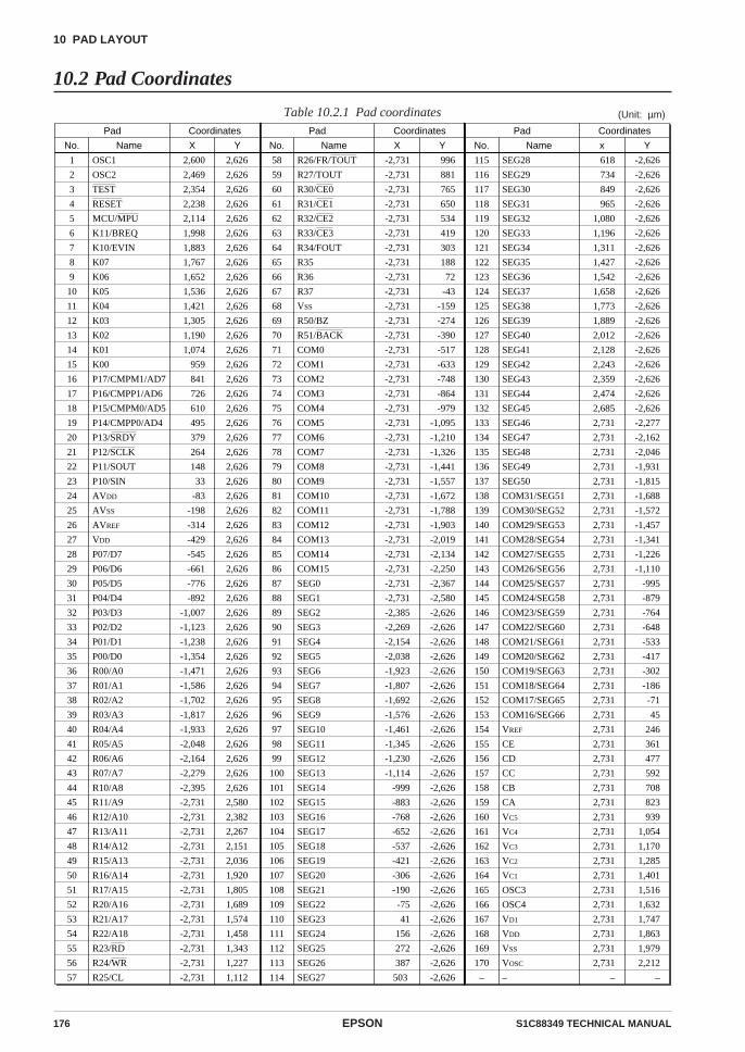
176 EPSON S1C88349 TECHNICAL MANUAL
10 PAD LAYOUT
10.2 Pad Coordinates
Table 10.2.1 Pad coordinates (Unit: µm)
No.
1
2
3
4
5
6
7
8
9
10
11
12
13
14
15
16
17
18
19
20
21
22
23
24
25
26
27
28
29
30
31
32
33
34
35
36
37
38
39
40
41
42
43
44
45
46
47
48
49
50
51
52
53
54
55
56
57
Name
OSC1
OSC2
TEST
RESET
MCU/MPU
K11/BREQ
K10/EVIN
K07
K06
K05
K04
K03
K02
K01
K00
P17/CMPM1/AD7
P16/CMPP1/AD6
P15/CMPM0/AD5
P14/CMPP0/AD4
P13/SRDY
P12/SCLK
P11/SOUT
P10/SIN
AVDD
AVSS
AVREF
VDD
P07/D7
P06/D6
P05/D5
P04/D4
P03/D3
P02/D2
P01/D1
P00/D0
R00/A0
R01/A1
R02/A2
R03/A3
R04/A4
R05/A5
R06/A6
R07/A7
R10/A8
R11/A9
R12/A10
R13/A11
R14/A12
R15/A13
R16/A14
R17/A15
R20/A16
R21/A17
R22/A18
R23/RD
R24/WR
R25/CL
X
2,600
2,469
2,354
2,238
2,114
1,998
1,883
1,767
1,652
1,536
1,421
1,305
1,190
1,074
959
841
726
610
495
379
264
148
33
-83
-198
-314
-429
-545
-661
-776
-892
-1,007
-1,123
-1,238
-1,354
-1,471
-1,586
-1,702
-1,817
-1,933
-2,048
-2,164
-2,279
-2,395
-2,731
-2,731
-2,731
-2,731
-2,731
-2,731
-2,731
-2,731
-2,731
-2,731
-2,731
-2,731
-2,731
Y
2,626
2,626
2,626
2,626
2,626
2,626
2,626
2,626
2,626
2,626
2,626
2,626
2,626
2,626
2,626
2,626
2,626
2,626
2,626
2,626
2,626
2,626
2,626
2,626
2,626
2,626
2,626
2,626
2,626
2,626
2,626
2,626
2,626
2,626
2,626
2,626
2,626
2,626
2,626
2,626
2,626
2,626
2,626
2,626
2,580
2,382
2,267
2,151
2,036
1,920
1,805
1,689
1,574
1,458
1,343
1,227
1,112
Pad Coordinates
No.
58
59
60
61
62
63
64
65
66
67
68
69
70
71
72
73
74
75
76
77
78
79
80
81
82
83
84
85
86
87
88
89
90
91
92
93
94
95
96
97
98
99
100
101
102
103
104
105
106
107
108
109
110
111
112
113
114
Name
R26/FR/TOUT
R27/TOUT
R30/CE0
R31/CE1
R32/CE2
R33/CE3
R34/FOUT
R35
R36
R37
VSS
R50/BZ
R51/BACK
COM0
COM1
COM2
COM3
COM4
COM5
COM6
COM7
COM8
COM9
COM10
COM11
COM12
COM13
COM14
COM15
SEG0
SEG1
SEG2
SEG3
SEG4
SEG5
SEG6
SEG7
SEG8
SEG9
SEG10
SEG11
SEG12
SEG13
SEG14
SEG15
SEG16
SEG17
SEG18
SEG19
SEG20
SEG21
SEG22
SEG23
SEG24
SEG25
SEG26
SEG27
X
-2,731
-2,731
-2,731
-2,731
-2,731
-2,731
-2,731
-2,731
-2,731
-2,731
-2,731
-2,731
-2,731
-2,731
-2,731
-2,731
-2,731
-2,731
-2,731
-2,731
-2,731
-2,731
-2,731
-2,731
-2,731
-2,731
-2,731
-2,731
-2,731
-2,731
-2,731
-2,385
-2,269
-2,154
-2,038
-1,923
-1,807
-1,692
-1,576
-1,461
-1,345
-1,230
-1,114
-999
-883
-768
-652
-537
-421
-306
-190
-75
41
156
272
387
503
Y
996
881
765
650
534
419
303
188
72
-43
-159
-274
-390
-517
-633
-748
-864
-979
-1,095
-1,210
-1,326
-1,441
-1,557
-1,672
-1,788
-1,903
-2,019
-2,134
-2,250
-2,367
-2,580
-2,626
-2,626
-2,626
-2,626
-2,626
-2,626
-2,626
-2,626
-2,626
-2,626
-2,626
-2,626
-2,626
-2,626
-2,626
-2,626
-2,626
-2,626
-2,626
-2,626
-2,626
-2,626
-2,626
-2,626
-2,626
-2,626
Pad Coordinates
No.
115
116
117
118
119
120
121
122
123
124
125
126
127
128
129
130
131
132
133
134
135
136
137
138
139
140
141
142
143
144
145
146
147
148
149
150
151
152
153
154
155
156
157
158
159
160
161
162
163
164
165
166
167
168
169
170
–
Name
SEG28
SEG29
SEG30
SEG31
SEG32
SEG33
SEG34
SEG35
SEG36
SEG37
SEG38
SEG39
SEG40
SEG41
SEG42
SEG43
SEG44
SEG45
SEG46
SEG47
SEG48
SEG49
SEG50
COM31/SEG51
COM30/SEG52
COM29/SEG53
COM28/SEG54
COM27/SEG55
COM26/SEG56
COM25/SEG57
COM24/SEG58
COM23/SEG59
COM22/SEG60
COM21/SEG61
COM20/SEG62
COM19/SEG63
COM18/SEG64
COM17/SEG65
COM16/SEG66
VREF
CE
CD
CC
CB
CA
VC5
VC4
VC3
VC2
VC1
OSC3
OSC4
VD1
VDD
VSS
VOSC
–
x
618
734
849
965
1,080
1,196
1,311
1,427
1,542
1,658
1,773
1,889
2,012
2,128
2,243
2,359
2,474
2,685
2,731
2,731
2,731
2,731
2,731
2,731
2,731
2,731
2,731
2,731
2,731
2,731
2,731
2,731
2,731
2,731
2,731
2,731
2,731
2,731
2,731
2,731
2,731
2,731
2,731
2,731
2,731
2,731
2,731
2,731
2,731
2,731
2,731
2,731
2,731
2,731
2,731
2,731
–
Y
-2,626
-2,626
-2,626
-2,626
-2,626
-2,626
-2,626
-2,626
-2,626
-2,626
-2,626
-2,626
-2,626
-2,626
-2,626
-2,626
-2,626
-2,626
-2,277
-2,162
-2,046
-1,931
-1,815
-1,688
-1,572
-1,457
-1,341
-1,226
-1,110
-995
-879
-764
-648
-533
-417
-302
-186
-71
45
246
361
477
592
708
823
939
1,054
1,170
1,285
1,401
1,516
1,632
1,747
1,863
1,979
2,212
–
Pad Coordinates
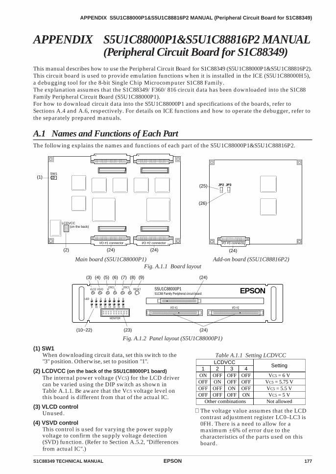
S1C88349 TECHNICAL MANUAL EPSON 177
APPENDIX S5U1C88000P1&S5U1C88816P2 MANUAL (Peripheral Circuit Board for S1C88349)
APPENDIX S5U1C88000P1&S5U1C88816P2 MANUAL(Peripheral Circuit Board for S1C88349)
This manual describes how to use the Peripheral Circuit Board for S1C88349 (S5U1C88000P1&S5U1C88816P2).This circuit board is used to provide emulation functions when it is installed in the ICE (S5U1C88000H5),a debugging tool for the 8-bit Single Chip Microcomputer S1C88 Family.The explanation assumes that the S1C88349/F360/816 circuit data has been downloaded into the S1C88Family Peripheral Circuit Board (S5U1C88000P1).For how to download circuit data into the S5U1C88000P1 and specifications of the boards, refer toSections A.4 and A.6, respectively. For details on ICE functions and how to operate the debugger, refer tothe separately prepared manuals.
A.1 Names and Functions of Each PartThe following explains the names and functions of each part of the S5U1C88000P1&S5U1C88816P2.
I/O #2 connector I/O #1 connector
SW1
LCDVCC (on the back)
(1)
(2) (24) (24)
I/O #3 connector
(24)
(25)
(26)
JP2 JP3JP2 JP3
RESET
MONITOR
L S5U1C88000P1S1C88 Family Peripheral circuit board EPSON
I/O #1
HOSC3
LHOSC1
VSVDVLCD
LED 87654321
161514131211109
(3) (4) (5) (6) (7) (8) (9)
(24)(23)(10~22)
(24)
I/O #2
Main board (S5U1C88000P1) Add-on board (S5U1C88816P2)Fig. A.1.1 Board layout
Fig. A.1.2 Panel layout (S5U1C88000P1)
(1) SW1When downloading circuit data, set this switch to the"3" position. Otherwise, set to position "1".
(2) LCDVCC (on the back of the S5U1C88000P1 board)The internal power voltage (VC5) for the LCD drivercan be varied using the DIP switch as shown inTable A.1.1. Be aware that the VC5 voltage level onthis board is different from that of the actual IC.
(3) VLCD controlUnused.
(4) VSVD controlThis control is used for varying the power supplyvoltage to confirm the supply voltage detection(SVD) function. (Refer to Section A.5.2, "Differencesfrom actual IC".)
Table A.1.1 Setting LCDVCCLCDVCC
Other combinations
Setting
VC5 = 6 VVC5 = 5.75 VVC5 = 5.5 VVC5 = 5 V
Not allowed
1 2 3 4ONOFFOFFOFF
OFFONOFFOFF
OFFOFFONOFF
OFFOFFOFFON
∗ The voltage value assumes that the LCDcontrast adjustment register LC0–LC3 is0FH. There is a need to allow for amaximum ±6% of error due to thecharacteristics of the parts used on thisboard.
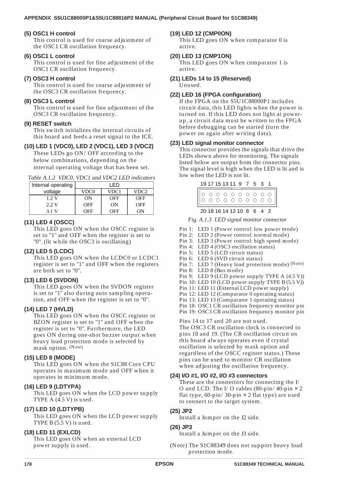
178 EPSON S1C88349 TECHNICAL MANUAL
APPENDIX S5U1C88000P1&S5U1C88816P2 MANUAL (Peripheral Circuit Board for S1C88349)
(5) OSC1 H controlThis control is used for coarse adjustment ofthe OSC1 CR oscillation frequency.
(6) OSC1 L controlThis control is used for fine adjustment of theOSC1 CR oscillation frequency.
(7) OSC3 H controlThis control is used for coarse adjustment ofthe OSC3 CR oscillation frequency.
(8) OSC3 L controlThis control is used for fine adjustment of theOSC3 CR oscillation frequency.
(9) RESET switchThis switch initializes the internal circuits ofthis board and feeds a reset signal to the ICE.
(10) LED 1 (VDC0), LED 2 (VDC1), LED 3 (VDC2)These LEDs go ON/OFF according to thebelow combinations, depending on theinternal operating voltage that has been set.
Table A.1.2 VDC0, VDC1 and VDC2 LED indicatorsLEDInternal operating
voltage1.2 V2.2 V3.1 V
VDC0ONOFFOFF
VDC1OFFONOFF
VDC2OFFOFFON
(11) LED 4 (OSCC)This LED goes ON when the OSCC register isset to "1" and OFF when the register is set to"0". (lit while the OSC3 is oscillating)
(12) LED 5 (LCDC)This LED goes ON when the LCDC0 or LCDC1register is set to "1" and OFF when the registersare both set to "0".
(13) LED 6 (SVDON)This LED goes ON when the SVDON registeris set to "1" also during auto sampling opera-tion, and OFF when the register is set to "0".
(14) LED 7 (HVLD)This LED goes ON when the OSCC register orBZON register is set to "1" and OFF when theregister is set to "0". Furthermore, the LEDgoes ON during one-shot buzzer output whenheavy load protection mode is selected bymask option. (Note)
(15) LED 8 (MODE)This LED goes ON when the S1C88 Core CPUoperates in maximum mode and OFF when itoperates in minimum mode.
(16) LED 9 (LDTYPA)This LED goes ON when the LCD power supplyTYPE A (4.5 V) is used.
(17) LED 10 (LDTYPB)This LED goes ON when the LCD power supplyTYPE B (5.5 V) is used.
(18) LED 11 (EXLCD)This LED goes ON when an external LCDpower supply is used.
(19) LED 12 (CMP0ON)This LED goes ON when comparator 0 isactive.
(20) LED 13 (CMP1ON)This LED goes ON when comparator 1 isactive.
(21) LEDs 14 to 15 (Reserved)Unused.
(22) LED 16 (FPGA configuration)If the FPGA on the S5U1C88000P1 includescircuit data, this LED lights when the power isturned on. If this LED does not light at power-up, a circuit data must be written to the FPGAbefore debugging can be started (turn thepower on again after writing data).
(23) LED signal monitor connectorThis connector provides the signals that drive theLEDs shown above for monitoring. The signalslisted below are output from the connector pins.The signal level is high when the LED is lit and islow when the LED is not lit.
2468101214161820
135791113151719
Fig. A.1.3 LED signal monitor connector
Pin 1: LED 1 (Power control: low power mode)Pin 2: LED 2 (Power control: normal mode)Pin 3: LED 3 (Power control: high speed mode)Pin 4: LED 4 (OSC3 oscillation status)Pin 5: LED 5 (LCD circuit status)Pin 6: LED 6 (SVD circuit status)Pin 7: LED 7 (Heavy load protection mode) (Note)
Pin 8: LED 8 (Bus mode)Pin 9: LED 9 (LCD power supply TYPE A (4.5 V))Pin 10: LED 10 (LCD power supply TYPE B (5.5 V))Pin 11: LED 11 (External LCD power supply)Pin 12: LED 12 (Comparator 0 operating status)Pin 13: LED 13 (Comparator 1 operating status)Pin 18: OSC1 CR oscillation frequency monitor pinPin 19: OSC3 CR oscillation frequency monitor pin
Pins 14 to 17 and 20 are not used.The OSC3 CR oscillation clock is connected topins 18 and 19. (The CR oscillation circuit onthis board always operates even if crystaloscillation is selected by mask option andregardless of the OSCC register status.) Thesepins can be used to monitor CR oscillationwhen adjusting the oscillation frequency.
(24) I/O #1, I/O #2, I/O #3 connectorsThese are the connectors for connecting the I/O and LCD. The I/O cables (80-pin/40-pin × 2flat type, 60-pin/30-pin × 2 flat type) are usedto connect to the target system.
(25) JP2Install a Jumper on the J2 side.
(26) JP3Install a Jumper on the J3 side.
(Note) The S1C88349 does not support heavy loadprotection mode.
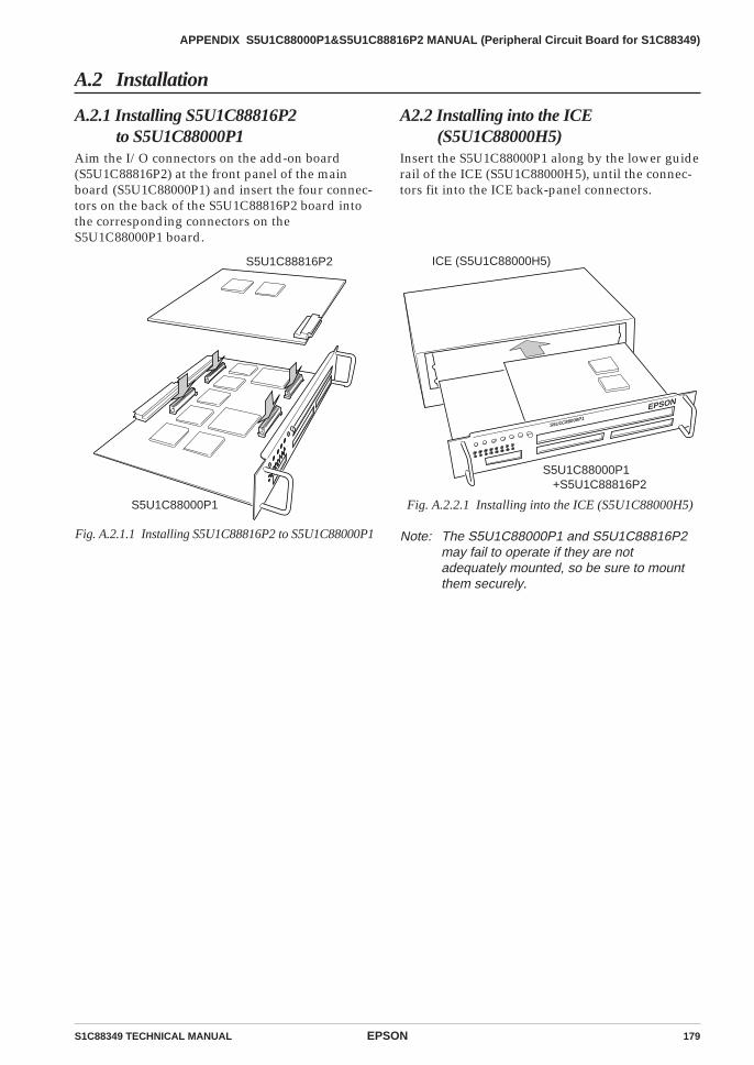
S1C88349 TECHNICAL MANUAL EPSON 179
APPENDIX S5U1C88000P1&S5U1C88816P2 MANUAL (Peripheral Circuit Board for S1C88349)
A.2 Installation
A.2.1 Installing S5U1C88816P2to S5U1C88000P1
Aim the I/O connectors on the add-on board(S5U1C88816P2) at the front panel of the mainboard (S5U1C88000P1) and insert the four connec-tors on the back of the S5U1C88816P2 board intothe corresponding connectors on theS5U1C88000P1 board.
S5U1C88000P1
S5U1C88816P2
Fig. A.2.1.1 Installing S5U1C88816P2 to S5U1C88000P1
A2.2 Installing into the ICE (S5U1C88000H5)
Insert the S5U1C88000P1 along by the lower guiderail of the ICE (S5U1C88000H5), until the connec-tors fit into the ICE back-panel connectors.
ICE (S5U1C88000H5)
S5U1C88000P1 +S5U1C88816P2
EPSON
S5U1C88000P1
Fig. A.2.2.1 Installing into the ICE (S5U1C88000H5)
Note: The S5U1C88000P1 and S5U1C88816P2may fail to operate if they are notadequately mounted, so be sure to mountthem securely.
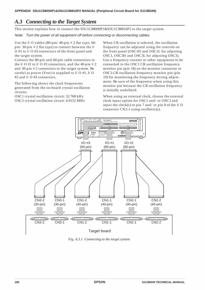
180 EPSON S1C88349 TECHNICAL MANUAL
APPENDIX S5U1C88000P1&S5U1C88816P2 MANUAL (Peripheral Circuit Board for S1C88349)
A.3 Connecting to the Target SystemThis section explains how to connect the S5U1C88000P1&S5U1C88816P2 to the target system.
Note: Turn the power of all equipment off before connecting or disconnecting cables.
Use the I/O cables (80-pin/40-pin × 2 flat type, 60-pin/30-pin × 2 flat type) to connect between the I/O #1 to I/O #3 connectors of the front panel andthe target system.Connect the 80-pin and 60-pin cable connectors tothe I/O #1 to I/O #3 connectors, and the 40-pin × 2and 30-pin × 2 connectors to the target system. Becareful as power (VDD) is supplied to I/O #1, I/O#2 and I/O #3 connectors.
The following shows the clock frequenciesgenerated from the on-board crystal oscillationcircuits:OSC1 crystal oscillation circuit: 32.768 kHzOSC3 crystal oscillation circuit: 4.9152 MHz
When CR oscillation is selected, the oscillationfrequency can be adjusted using the controls onthe front panel (OSC1H and OSC1L for adjustingOSC1, OSC3H and OSC3L for adjusting OSC3).Use a frequency counter or other equipment to beconnected to the OSC1 CR oscillation frequencymonitor pin (pin 18) on the monitor connector orOSC3 CR oscillation frequency monitor pin (pin19) for monitoring the frequency during adjust-ment. Be sure of the frequency when using thismonitor pin because the CR oscillation frequencyis initially undefined.
When using an external clock, choose the externalclock input option for OSC1 and/or OSC3 andinput the clock(s) to pin 7 and/or pin 8 of the I/Oconnector CN2-1 using oscillator(s).
POWER
EMU
SLP/H
ALT
RESET
TRGOUT
STOPOUT
TRCIN
BRKINGND
ICE88UR E0C88 Family In-Circuit Emulator
ON/OFF
DIAG
RESET
MONITOR
L S5U1C88000P1S1C88 Family Peripheral circuit board EPSON
I/O #2I/O #1
HOSC3
LHOSC1
VSVDVLCD
LCD 87654321
161514131211109
CN1-1(40-pin)
Target board
I/O #1(80-pin)
CN2-1(40-pin)
I/O #2(80-pin)
CN2-2(40-pin)
CN1-2(40-pin)
CN3-1(30-pin)
CN3-2(30-pin)
CN1-1 CN2-1 CN2-2CN1-2CN3-1CN3-2
I/O #3(60-pin)
Fig. A.3.1 Connecting to the target system
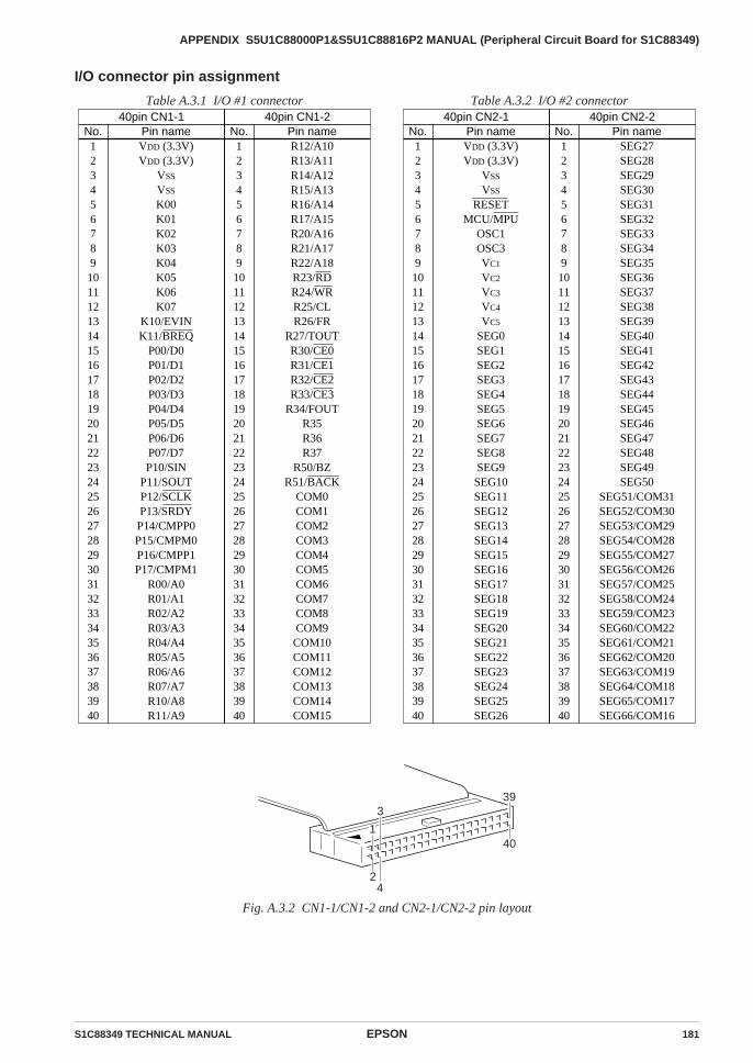
S1C88349 TECHNICAL MANUAL EPSON 181
APPENDIX S5U1C88000P1&S5U1C88816P2 MANUAL (Peripheral Circuit Board for S1C88349)
I/O connector pin assignment
Table A.3.2 I/O #2 connector
No.12345678910111213141516171819202122232425262728293031323334353637383940
Pin nameVDD (3.3V)VDD (3.3V)
VSS
VSS
RESETMCU/MPU
OSC1OSC3VC1
VC2
VC3
VC4
VC5
SEG0SEG1SEG2SEG3SEG4SEG5SEG6SEG7SEG8SEG9SEG10SEG11SEG12SEG13SEG14SEG15SEG16SEG17SEG18SEG19SEG20SEG21SEG22SEG23SEG24SEG25SEG26
No.12345678910111213141516171819202122232425262728293031323334353637383940
Pin nameSEG27SEG28SEG29SEG30SEG31SEG32SEG33SEG34SEG35SEG36SEG37SEG38SEG39SEG40SEG41SEG42SEG43SEG44SEG45SEG46SEG47SEG48SEG49SEG50
SEG51/COM31SEG52/COM30SEG53/COM29SEG54/COM28SEG55/COM27SEG56/COM26SEG57/COM25SEG58/COM24SEG59/COM23SEG60/COM22SEG61/COM21SEG62/COM20SEG63/COM19SEG64/COM18SEG65/COM17SEG66/COM16
40pin CN2-1 40pin CN2-2Table A.3.1 I/O #1 connector
No.12345678910111213141516171819202122232425262728293031323334353637383940
Pin nameVDD (3.3V)VDD (3.3V)
VSS
VSS
K00K01K02K03K04K05K06K07
K10/EVINK11/BREQ
P00/D0P01/D1P02/D2P03/D3P04/D4P05/D5P06/D6P07/D7P10/SIN
P11/SOUTP12/SCLKP13/SRDY
P14/CMPP0P15/CMPM0P16/CMPP1P17/CMPM1
R00/A0R01/A1R02/A2R03/A3R04/A4R05/A5R06/A6R07/A7R10/A8R11/A9
No.12345678910111213141516171819202122232425262728293031323334353637383940
Pin nameR12/A10R13/A11R14/A12R15/A13R16/A14R17/A15R20/A16R21/A17R22/A18R23/RDR24/WRR25/CLR26/FR
R27/TOUTR30/CE0R31/CE1R32/CE2R33/CE3
R34/FOUTR35R36R37
R50/BZR51/BACK
COM0COM1COM2COM3COM4COM5COM6COM7COM8COM9COM10COM11COM12COM13COM14COM15
40pin CN1-1 40pin CN1-2
3
1
2
39
40
4
Fig. A.3.2 CN1-1/CN1-2 and CN2-1/CN2-2 pin layout
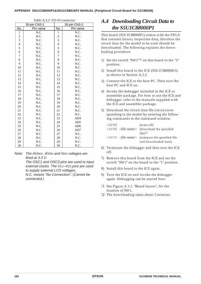
182 EPSON S1C88349 TECHNICAL MANUAL
APPENDIX S5U1C88000P1&S5U1C88816P2 MANUAL (Peripheral Circuit Board for S1C88349)
Table A.3.3 I/O #3 connector
No.123456789101112131415161718192021222324252627282930
Pin nameN.C.N.C.N.C.N.C.N.C.N.C.N.C.N.C.N.C.N.C.N.C.N.C.N.C.N.C.N.C.N.C.N.C.N.C.N.C.N.C.N.C.N.C.N.C.N.C.N.C.N.C.N.C.N.C.N.C.N.C.
No.123456789101112131415161718192021222324252627282930
Pin nameN.C.N.C.N.C.N.C.N.C.N.C.N.C.N.C.N.C.N.C.N.C.N.C.N.C.N.C.N.C.N.C.N.C.N.C.N.C.N.C.N.C.N.C.AD4AD5AD6AD7N.C.N.C.N.C.N.C.
30-pin CN3-1 30-pin CN3-2
Note: The AVREF, AVDD and VDD voltages arefixed at 3.3 V.The OSC1 and OSC3 pins are used to inputexternal clocks. The VC1–VC5 pins are usedto supply external LCD voltages.N.C. means "No Connection". (Cannot beconnected.)
A.4 Downloading Circuit Data tothe S5U1C88000P1
This board (S5U1C88000P1) comes with the FPGAthat contains factory inspection data, therefore thecircuit data for the model to be used should bedownloaded. The following explains the down-loading procedure.
1) Set the switch "SW1"∗ 1 on this board to the "3"position.
2) Install this board to the ICE (S5U1C88000H5)as shown in Section A.2.2.
3) Connect the ICE to the host PC. Then turn thehost PC and ICE on.
4) Invoke the debugger included in the ICE orassembler package. For how to use the ICE anddebugger, refer to the manuals supplied withthe ICE and assembler package.
5) Download the circuit data file (.mcs) corre-sponding to the model by entering the follow-ing commands in the command window.
>XFER (erase all)>XFWR <file name> (download the specified
file)∗ 2
>XFCP <file name> (compare the specified fileand downloaded data)
6) Terminate the debugger and then turn the ICEoff.
7) Remove this board from the ICE and set theswitch "SW1" on the board to the "1" position.
8) Install this board to the ICE again.
9) Turn the ICE on and invoke the debuggeragain. Debugging can be started here.
∗ 1 See Figure A.1.1, "Board layout", for thelocation of SW1.
∗ 2 The downloading takes about 5 minutes.
S1C88349 TECHNICAL MANUAL EPSON 183
APPENDIX S5U1C88000P1&S5U1C88816P2 MANUAL (Peripheral Circuit Board for S1C88349)
A.5 PrecautionsTake the following precautions when using theS5U1C88000P1&S5U1C88816P2.
A.5.1 Precaution for operation(1) Turn the power of all equipment off before
connecting or disconnecting cables.
(2) Turn the VSVD control on the front panelclockwise until it clicks before starting thedebugger.
(3) The mask option data must be loaded beforedebugging can be started.
A.5.2 Differences from actual ICCaution is called for due to the following functionand property related differences with the actualIC. If these precautions are overlooked, it may notoperate on the actual IC, even if it operates on theICE in which the S5U1C88000P1&S5U1C88816P2has been installed.
(1) I/O differencesInterface power voltage
This board and target system interface voltageis set to +3.3 V. To obtain the same interfacevoltage as in the actual IC, attach a level shifteror similar circuit on the target system side toaccommodate the required interface voltage.
Drive capability of each output portThe drive capability of each output port on thisboard is higher than that of the actual IC.When designing the application system andsoftware, refer to Chapter 8, "ELECTRICALCHARACTERISTICS" to confirm the drivecapability of each output port.
(2) Differences in current consumptionThe amount of current consumed by this boarddiffers significantly from that of the actual IC.Inspecting the LEDs on the S5U1C88000P1front panel may help keep track of approxi-mate current consumption. The followingfactors/components greatly affect devicecurrent consumption:
Those which can be verified by LEDsand monitor pins
a) Power supply control: low power mode(LED 1/monitor pin 1)
b) Power supply control: normal mode(LED 2/monitor pin 2)
c) Power supply control: high speed mode(LED 3/monitor pin 3)
d) OSC3 oscillation on/off control(LED 4/monitor pin 4)
e) LCD drive control(LED 5/monitor pin 5)
f) SVD circuit on/off control(LED 6/monitor pin 6)
g) Maximum mode(LED 8/monitor pin 8)
h) LCD power supply TYPE A(LED 9/monitor pin 9)
i) LCD power supply TYPE B(LED 10/monitor pin 10)
j) External LCD power supply(LED 11/monitor pin 11)
k) Comparator 0 on/off control(LED 12/monitor pin 12)
l) Comparator 1 on/off control(LED 13/monitor pin 13)
(3) Functional precautionsLCD circuit • Pay attention to the output drive capability
and output voltage of the LCD terminals (SEG,COM), since they are different from those ofthe actual IC. When an internal LCD poweroption is selected using winfog, this boardgenerates the same LCD drive voltage regard-less of the selected voltage (4.5 V or 5.5 V).However, the selected voltage level is indicatedwith the LED. The system and the softwareshould be designed in order to adjust the LCDcontrast. The S5U1C88000P1 board allowsswitching of the LCD drive voltage with itsswitch on the back side. (Refer to Section A.1,"Names and Functions of Each Part".)
• When the LCDC0 and LCDC1 registers areboth set to "0" (LCD power control circuit isoff), the SEG and COM terminal outputs of theactual IC are fixed at VSS level. Note, however,that the COM outputs are fixed at VC4 leveland the SEG outputs are fixed at VC3 (or VC2for 1/4 bias) level in this board.
SVD circuit • The SVD function is realized by artificially
varying the power supply voltage using theVSVD control on the front panel of theS5U1C88000P1.
• There is a finite delay time from when thepower to the SVD circuit turns on until actualdetection of the voltage. The delay time on thisboard differs from that of the actual IC. Referto Chapter 8, "ELECTRICAL CHARACTERIS-TICS" when setting the appropriate wait timefor the actual IC.
Oscillation circuit • The OSC1 crystal oscillation frequency is fixed
at 32.768 kHz.
• The OSC1 CR oscillation frequency can beadjusted in the range of approx. 20 kHz to 500kHz using the control on the S5U1C88000P1front panel. Note that the actual IC does notoperate with all of these frequencies; refer toChapter 8, "ELECTRICAL CHARACTERIS-TICS" to select the appropriate operatingfrequency.
• The OSC3 crystal oscillation frequency is fixedat 4.9152 MHz.
184 EPSON S1C88349 TECHNICAL MANUAL
APPENDIX S5U1C88000P1&S5U1C88816P2 MANUAL (Peripheral Circuit Board for S1C88349)
• The OSC3 CR oscillation frequency can beadjusted in the range of approx. 100 kHz to 8MHz using the control on the S5U1C88000P1front panel. Note that the actual IC does notoperate with all of these frequencies; refer toChapter 8, "ELECTRICAL CHARACTERISTICS"to select the appropriate operating frequency.
• The S5U1C88000P1&S5U1C88816P2 does notinclude the OSC3 ceramic oscillation circuit.When ceramic oscillation circuit is selected bymask option, this board uses the on-board CRoscillation circuit. Therefore, adjust theoscillation frequency using the control on theS5U1C88000P1 front panel before debugging.
• When using an external clock, adjust theexternal clock (amplitude: 3.3 V ±5%, duty:50% ±10%) and input to the OSC1 or OSC3terminal with VSS as GND.
• This board can operate normally even when theCPU clock is switched to OSC3 (CLKCHG = "1")immediately after the OSC3 oscillation controlcircuit is turned on (OSCC = "1") without a waittime inserted. In the actual IC, an oscillationstability wait time is required before switchingthe CPU clock after the OSC3 oscillation isturned on. Refer to Chapter 8, "ELECTRICALCHARACTERISTICS" when setting the appro-priate wait time for the actual IC.
• Use separate instructions to switch the clockfrom OSC3 to OSC1 and to turn off the OSC3oscillation circuit. If executed simultaneouslywith a single instruction, these operations,although good with this board, may notfunction properly with the actual IC.
• This board contains oscillation circuits forOSC1 and OSC3. Keep in mind that eventhough the actual IC may not have a resonatorconnected to its OSC3, this board can operatewith the OSC3 circuit.
• Because the logic level of the oscillation circuit ishigh, the timing at which the oscillation starts onthis board differs from that of the actual IC. Beaware that the CR oscillation does not stop evenif the SLP instruction is executed and the monitorpin keeps outputting the oscillation clock.
Access to undefined address spaceIf any undefined space in the S1C88349's internalROM/RAM or I/O is accessed for data read orwrite operations, the read/written value isindeterminate. Additionally, it is important toremain aware that the indeterminate state differsbetween this board and the actual IC.
Reset circuitKeep in mind that the operation sequence fromwhen the ICE with this board installed ispowered on until the time at which theprogram starts running differs from thesequence of the actual IC. This is because thisboard becomes capable of operating as adebugging system after the user program andoptional data are downloaded.
Internal power supply circuit • Since this board does not actually change the
internal operating voltage level (the voltagelevel is fixed at the value that enables opera-tion for all modes), it can operate normally ifthe software specifies an invalid voltage level.The actual IC needs to set the internal operat-ing voltage to the valid level according to theoperating mode. Be sure to refer to Chapter 8,"ELECTRICAL CHARACTERISTICS" whensetting the correct voltage. Also, when switch-ing the control voltages, consult the technicalmanual to determine the appropriate wait timeto be inserted.
• Since the usable operating frequency rangedepends on the device's internal operatingvoltage, consult Chapter 8, "ELECTRICALCHARACTERISTICS" to ensure that the devicewill not be operated with an inappropriatecombination of operating frequency andinternal power supply.
• The LCD drive voltage on this board isdifferent from that on the actual IC.
(4) Notes on model supportParameter file
The ROM, RAM and I/O spaces in the ICE withthis board installed are configured when thedebugger on the personal computer starts upusing the parameter file (88349.par) provided foreach model.The parameter file allows the user to modify itscontents according to the ROM and RAM spacesactually used. However, do not configure areasother than below.ROM area: 0000H to BFFFHRAM area: F000H to F7FFHStack area: F000H to F7FFH
Access disable areaWhen using this board for development of anS1C88349 application, be sure not to read andwrite from/to I/O memory addresses FF46Hand FF47H.
(5) Precautions on replacementS5U1C88816P1 withS5U1C88000P1+S5U1C88816P2
• In S5U1C88816P1, the AD4–AD7 analog inputpins are shared with the P14–P17 I/O portpins. In S5U1C88000P1+S5U1C88816P2, theAD4–AD7 pins are assigned in the I/O #3connector and the P14–P17 pins are assigned inthe I/O #1 connector. Pay attention to theconnection to the target board.
• The I/O voltage is different; it is 5 V inS5U1C88816P1 and 3.3 V inS5U1C88000P1+S5U1C88816P2.
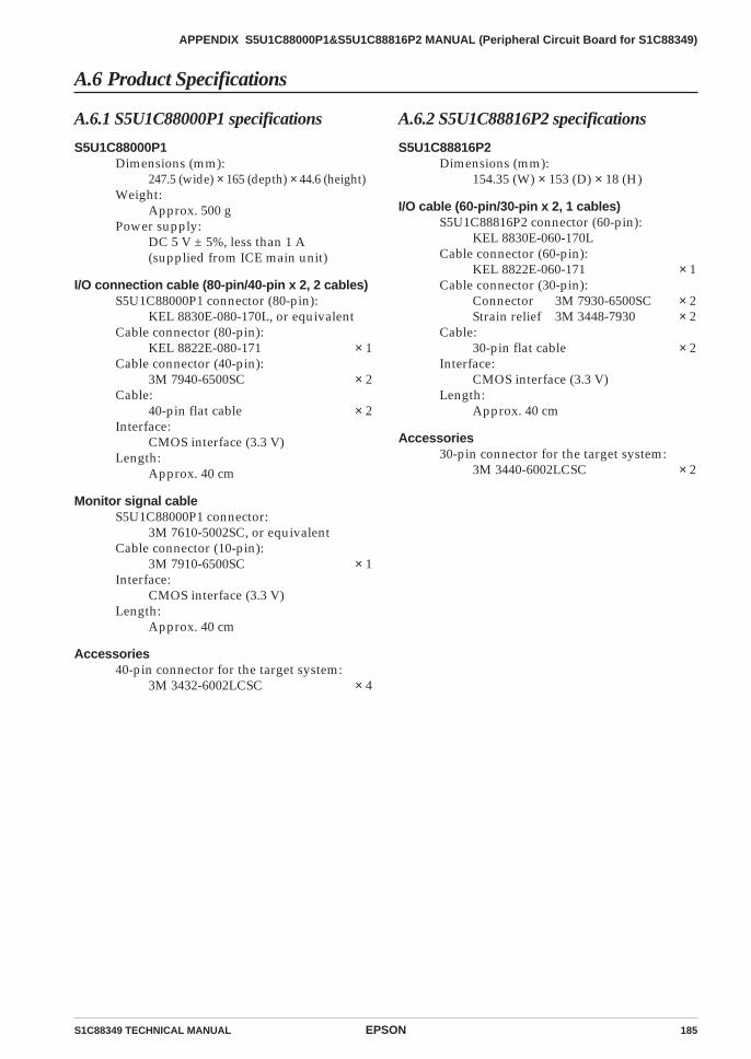
S1C88349 TECHNICAL MANUAL EPSON 185
APPENDIX S5U1C88000P1&S5U1C88816P2 MANUAL (Peripheral Circuit Board for S1C88349)
A.6 Product Specifications
A.6.2 S5U1C88816P2 specifications
S5U1C88816P2Dimensions (mm):
154.35 (W) × 153 (D) × 18 (H)
I/O cable (60-pin/30-pin x 2, 1 cables)S5U1C88816P2 connector (60-pin):
KEL 8830E-060-170LCable connector (60-pin):
KEL 8822E-060-171 × 1Cable connector (30-pin):
Connector 3M 7930-6500SC × 2Strain relief 3M 3448-7930 × 2
Cable:30-pin flat cable × 2
Interface:CMOS interface (3.3 V)
Length:Approx. 40 cm
Accessories30-pin connector for the target system:
3M 3440-6002LCSC × 2
A.6.1 S5U1C88000P1 specifications
S5U1C88000P1Dimensions (mm):
247.5 (wide) × 165 (depth) × 44.6 (height)Weight:
Approx. 500 gPower supply:
DC 5 V ± 5%, less than 1 A(supplied from ICE main unit)
I/O connection cable (80-pin/40-pin x 2, 2 cables)S5U1C88000P1 connector (80-pin):
KEL 8830E-080-170L, or equivalentCable connector (80-pin):
KEL 8822E-080-171 × 1Cable connector (40-pin):
3M 7940-6500SC × 2Cable:
40-pin flat cable × 2Interface:
CMOS interface (3.3 V)Length:
Approx. 40 cm
Monitor signal cableS5U1C88000P1 connector:
3M 7610-5002SC, or equivalentCable connector (10-pin):
3M 7910-6500SC × 1Interface:
CMOS interface (3.3 V)Length:
Approx. 40 cm
Accessories40-pin connector for the target system:
3M 3432-6002LCSC × 4

AMERICA
EPSON ELECTRONICS AMERICA, INC.
- HEADQUARTERS -150 River Oaks ParkwaySan Jose, CA 95134, U.S.A.Phone: +1-800-228-3964 Fax: +1-408-922-0238
- SALES OFFICES -
West1960 E.Grand Avenue Flr 2El Segundo, CA 90245, U.S.A.Phone: +1-800-249-7730 Fax: +1-310-955-5400
Central101 Virginia Street, Suite 290Crystal Lake, IL 60014, U.S.A.Phone: +1-800-853-3588 Fax: +1-815-455-7633
Northeast301 Edgewater Place, Suite 210Wakefield, MA 01880, U.S.A.Phone: +1-800-922-7667 Fax: +1-781-246-5443
Southeast3010 Royal Blvd. South, Suite 170Alpharetta, GA 30005, U.S.A.Phone: +1-877-332-0020 Fax: +1-770-777-2637
EUROPE
EPSON EUROPE ELECTRONICS GmbH
- HEADQUARTERS -Riesstrasse 1580992 Munich, GERMANYPhone: +49-89-14005-0 Fax: +49-89-14005-110
DÜSSELDORF BRANCH OFFICEAltstadtstrasse 17651379 Leverkusen, GERMANYPhone: +49-2171-5045-0 Fax: +49-2171-5045-10
FRENCH BRANCH OFFICE1 Avenue de l’ Atlantique, LP 915 Les ConquerantsZ.A. de Courtaboeuf 2, F-91976 Les Ulis Cedex, FRANCEPhone: +33-1-64862350 Fax: +33-1-64862355
BARCELONA BRANCH OFFICEBarcelona Design CenterEdificio Testa, C/Alcalde Barnils 64-68, Modulo C 2a plantaE-08190 Sant Cugat del Vallès, SPAINPhone: +34-93-544-2490 Fax: +34-93-544-2491
UK & IRELAND BRANCH OFFICE8 The Square, Stockley Park, UxbridgeMiddx UB11 1FW, UNITED KINGDOMPhone: +44-1295-750-216/+44-1342-824451Fax: +44-89-14005 446/447
Scotland Design CenterIntegration House, The Alba CampusLivingston West Lothian, EH54 7EG, SCOTLANDPhone: +44-1506-605040 Fax: +44-1506-605041
ASIA
EPSON (CHINA) CO., LTD.23F, Beijing Silver Tower 2# North RD DongSanHuanChaoYang District, Beijing, CHINAPhone: +86-10-6410-6655 Fax: +86-10-6410-7320
SHANGHAI BRANCH7F, High-Tech Bldg., 900, Yishan RoadShanghai 200233, CHINAPhone: +86-21-5423-5522 Fax: +86-21-5423-5512
EPSON HONG KONG LTD.20/F, Harbour Centre, 25 Harbour RoadWanchai, Hong KongPhone: +852-2585-4600 Fax: +852-2827-4346Telex: 65542 EPSCO HX
EPSON TAIWAN TECHNOLOGY & TRADING LTD.14F, No. 7, Song Ren RoadTaipei 110Phone: +886-2-8786-6688 Fax: +886-2-8786-6677
HSINCHU OFFICENo. 99, Jiangong RoadHsinchu City 300Phone: +886-3-573-9900 Fax: +886-3-573-9169
EPSON SINGAPORE PTE., LTD.401 Commonwealth Drive, #07-01Haw Par Technocentre, SINGAPORE 149598Phone: +65-6586-3100 Fax: +65-6472-4291
SEIKO EPSON CORPORATION KOREA OFFICE50F, KLI 63 Bldg., 60 Yoido-dongYoungdeungpo-Ku, Seoul, 150-763, KOREAPhone: +82-2-784-6027 Fax: +82-2-767-3677
GUMI OFFICE6F, Good Morning Securities Bldg., 56 Songjeong-DongGumi-City, Seoul, 730-090, KOREAPhone: +82-54-454-6027 Fax: +82-54-454-6093
SEIKO EPSON CORPORATIONELECTRONIC DEVICES MARKETING & SALES DIV.
ED International Sales Dept.421-8, Hino, Hino-shi, Tokyo 191-8501, JAPANPhone: +81-42-587-5814 Fax: +81-42-587-5117
International Sales Operations

EPSON Electronic Devices Website
ELECTRONIC DEVICES MARKETING DIVISION
http://www.epsondevice.com
Technical ManualS1C88349
First issue May, 2001Printed November, 2004 in Japan AL
M
Document code: 404522102