Embed Size (px)
Citation preview
Datasheet
www.renesas.com
S3A1 Microcontroller Group
Datasheet
Renesas Synergy™ PlatformSynergy MicrocontrollersS3 Series
Oct 2018Rev.1.20
All information contained in these materials, including products and product specifications,represents information on the product at the time of publication and is subject to change byRenesas Electronics Corp. without notice. Please review the latest information published byRenesas Electronics Corp. through various means, including the Renesas Electronics Corp.website (http://www.renesas.com).
Cover
R01DS0324EU0120 Rev.1.20 Page 2 of 137Oct 29, 2018
Features■ Arm Cortex-M4 Core with Floating Point Unit (FPU) Armv7E-M architecture with DSP instruction set Maximum operating frequency: 48 MHz Support for 4-GB address space Arm Memory Protection Unit (Arm MPU) with 8 regions Debug and Trace: ITM, DWT, FPB, TPIU, ETB CoreSight™ Debug Port: JTAG-DP and SW-DP
■ Memory 1-MB code flash memory 8-KB data flash memory (100,000 program/erase (P/E) cycles) 192-KB SRAM Flash Cache (FCACHE) Memory Protection Unit (MPU) Memory Mirror Function (MMF) 128-bit unique ID
■ Connectivity USB 2.0 Full-Speed Module (USBFS)
- On-chip transceiver with voltage regulator- Compliant with USB Battery Charging Specification 1.2
Serial Communications Interface (SCI) × 6- UART- Simple IIC- Simple SPI
Serial Peripheral Interface (SPI) × 2 I2C bus interface (IIC) × 3 Controller Area Network (CAN) module Serial Sound Interface Enhanced (SSIE) SD/MMC Host Interface (SDHI) Quad Serial Peripheral Interface (QSPI) External address space
- 8- or 16-bit bus space is selectable per area
■ Analog 14-bit A/D Converter (ADC14) 12-bit D/A Converter (DAC12) 8-bit D/A Converter (DAC8) × 2 (for ACMPLP) Low-Power Analog Comparator (ACMPLP) × 2 Operational Amplifier (OPAMP) × 4 Temperature Sensor (TSN)
■ Timers General PWM Timer 32-Bit (GPT32) × 4 General PWM Timer 16-Bit (GPT16) × 6 Asynchronous General-Purpose Timer (AGT) × 2 Watchdog Timer (WDT)
■ Safety Error Correction Code (ECC) in SRAM SRAM parity error check Flash area protection ADC self-diagnosis function Clock Frequency Accuracy Measurement Circuit (CAC) Cyclic Redundancy Check (CRC) calculator Data Operation Circuit (DOC) Port Output Enable for GPT (POEG) Independent Watchdog Timer (IWDT) GPIO readback level detection Register write protection Main oscillator stop detection Illegal memory access
■ System and Power Management Low power modes Realtime Clock (RTC) with calendar and Battery Backup support Event Link Controller (ELC) DMA Controller (DMAC) × 4 Data Transfer Controller (DTC) Key Interrupt Function (KINT) Power-on reset Low Voltage Detection (LVD) with voltage settings
■ Security and Encryption AES128/256 GHASH True Random Number Generator (TRNG)
■ Human Machine Interface (HMI) Segment LCD Controller (SLCDC)
- Up to 54 segments × 4 commons- Up to 50 segments × 8 commons
Capacitive Touch Sensing Unit (CTSU)
■ Multiple Clock Sources Main clock oscillator (MOSC)
(1 to 20 MHz when VCC = 2.4 to 5.5 V)(1 to 8 MHz when VCC = 1.8 to 2.4 V)(1 to 4 MHz when VCC = 1.6 to 1.8 V)
Sub-clock oscillator (SOSC) (32.768 kHz) High-speed on-chip oscillator (HOCO)
(24, 32, 48, 64 MHz when VCC = 2.4 to 5.5 V)(24, 32, 48 MHz when VCC = 1.8 to 5.5 V)(24, 32 MHz when VCC = 1.6 to 5.5 V)
Middle-speed on-chip oscillator (MOCO) (8 MHz) Low-speed on-chip oscillator (LOCO) (32.768 kHz) IWDT-dedicated on-chip oscillator (15 kHz) Clock trim function for HOCO/MOCO/LOCO Clock out support
■ General Purpose I/O Ports Up to 126 input/output pins
- Up to 3 CMOS input- Up to 123 CMOS input/output - Up to 11 input/output 5-V tolerant - Up to 2 high current (20 mA)
■ Operating Voltage VCC: 1.6 to 5.5 V
■ Operating Temperature and Packages Ta = -40°C to +85°C
- 145-pin LGA (7 mm × 7 mm, 0.5 mm pitch)- 121-pin BGA (8 mm × 8 mm, 0.65 mm pitch)- 100-pin LGA (7 mm × 7 mm, 0.65 mm pitch)
Ta = -40°C to +105°C- 144-pin LQFP (20 mm × 20 mm, 0.5 mm pitch)- 100-pin LQFP (14 mm × 14 mm, 0.5 mm pitch)- 64-pin LQFP (10 mm × 10 mm, 0.5 mm pitch)- 64-pin QFN (8 mm × 8 mm, 0.4 mm pitch)
High efficiency 48-MHz Arm® Cortex®-M4 core, 1-MB code flash memory, 192-KB SRAM, Segment LCD Controller, Capacitive Touch Sensing Unit, USB 2.0 Full-Speed Module, 14-bit A/D Converter, 12-bit D/A Converter, security and safety features
S3A1 Microcontroller Group
Datasheet
Features
R01DS0324EU0120 Rev.1.20 Page 3 of 137Oct 29, 2018
S3A1 Datasheet 1. Overview
1. OverviewThe MCU integrates multiple series of software- and pin-compatible Arm®-based 32-bit cores that share a common set of Renesas peripherals to facilitate design scalability and efficient platform-based product development.
The MCU in this series incorporates a low-power, high-performance Arm Cortex®-M4 core running up to 48 MHz, with the following features:
1-MB code flash memory
192-KB SRAM
Segment LCD Controller (SLCDC)
Capacitive Touch Sensing Unit (CTSU)
USB 2.0 Full-Speed Module (USBFS)
14-bit A/D Converter (ADC14)
12-bit D/A Converter (DAC12)
Security features.
1.1 Function Outline
Table 1.1 Arm core
Feature Functional description
Arm Cortex-M4 Maximum operating frequency: up to 48 MHz Arm Cortex-M4
- Revision: r0p1-01rel0- Armv7E-M architecture profile- Single precision floating-point unit compliant with the ANSI/IEEE Std 754-2008.
Arm Memory Protection Unit (Arm MPU)- Armv7 Protected Memory System Architecture- 8 protected regions.
SysTick timer- Driven by SYSTICCLK (LOCO) or ICLK.
Table 1.2 Memory
Feature Functional description
Code flash memory Maximum 1-MB code flash memory. See section 47, Flash Memory in User’s Manual.
Data flash memory 8-KB data flash memory. See section 47, Flash Memory in User’s Manual.
Option-setting memory The option-setting memory determines the state of the MCU after a reset. See section 7, Option-Setting Memory in User’s Manual.
Memory Mirror Function (MMF) The Memory Mirror Function (MMF) can be configured to mirror the target application image load address in code flash memory to the application image link address in the 23-bit unused memory space (memory mirror space addresses). Your application code is developed and linked to run from this MMF destination address. The application code does not need to know the load location where it is stored in code flash memory. See section 5, Memory Mirror Function (MMF) in User’s Manual.
SRAM On-chip high-speed SRAM with either parity bit or Error Correction Code (ECC). The first 16-KB in SRAM0 provides error correction capability using ECC. See section 46, SRAM in User’s Manual.
R01DS0324EU0120 Rev.1.20 Page 4 of 137Oct 29, 2018
S3A1 Datasheet 1. Overview
Table 1.3 System (1 of 2)
Feature Functional description
Operating modes Two operating modes: Single-chip mode SCI/USB boot mode.See section 3, Operating Modes in User’s Manual.
Resets 14 resets: RES pin reset Power-on reset VBATT-selected voltage power-on reset Independent watchdog timer reset Watchdog timer reset Voltage monitor 0 reset Voltage monitor 1 reset Voltage monitor 2 reset SRAM parity error reset SRAM ECC error reset Bus master MPU error reset Bus slave MPU error reset CPU stack pointer error reset Software reset.See section 6, Resets in User’s Manual.
Low Voltage Detection (LVD) Low Voltage Detection (LVD) function monitors the voltage level input to the VCC pin, and the detection level can be selected using a software program. See section 8, Low Voltage Detection (LVD) in User’s Manual.
Clocks Main clock oscillator (MOSC) Sub-clock oscillator (SOSC) High-speed on-chip oscillator (HOCO) Middle-speed on-chip oscillator (MOCO) Low-speed on-chip oscillator (LOCO) PLL frequency synthesizer IWDT-dedicated on-chip oscillator Clock out support.See section 9, Clock Generation Circuit in User’s Manual.
Clock Frequency Accuracy Measurement Circuit (CAC)
The Clock Frequency Accuracy Measurement Circuit (CAC) counts pulses of the clock to be measured (measurement target clock) within the time generated by the clock to be used as a measurement reference (measurement reference clock), and determines the accuracy depending on whether the number of pulses is within the allowable range.When measurement is complete or the number of pulses within the time generated by the measurement reference clock is not within the allowable range, an interrupt request is generated.See section 10, Clock Frequency Accuracy Measurement Circuit (CAC) in User’s Manual.
Interrupt Controller Unit (ICU) The Interrupt Controller Unit (ICU) controls which event signals are linked to the NVIC/DTC module and DMAC module. The ICU also controls NMI interrupts. See section 14, Interrupt Controller Unit (ICU) in User’s Manual.
Key Interrupt Function (KINT) A key interrupt can be generated by setting the Key Return Mode Register (KRM) and inputting a rising or falling edge to the key interrupt input pins. See section 21, Key Interrupt Function (KINT) in User’s Manual.
Low power modes Power consumption can be reduced in multiple ways, such as by setting clock dividers, controlling EBCLK output, stopping modules, selecting power control mode in normal operation, and transitioning to low power modes. See section 11, Low Power Modes in User’s Manual.
Battery backup function A battery backup function is provided for partial powering by a battery. The battery powered area includes the RTC, SOSC, LOCO, wakeup control, backup memory, VBATT_R low voltage detection, and switches between VCC and VBATT.During normal operation, the battery powered area is powered by the main power supply, which is the VCC pin. When a VCC voltage drop is detected, the power source is switched to the dedicated battery backup power pin, the VBATT pin.When the voltage rises again, the power source is switched from the VBATT pin to the VCC pin. See section 12, Battery Backup Function in User’s Manual.
Register write protection The register write protection function protects important registers from being overwritten because of software errors. See section 13, Register Write Protection in User’s Manual.
R01DS0324EU0120 Rev.1.20 Page 5 of 137Oct 29, 2018
S3A1 Datasheet 1. Overview
Memory Protection Unit (MPU) Four Memory Protection Units (MPUs) and a CPU stack pointer monitor function are provided for memory protection. See section 16, Memory Protection Unit (MPU) in User’s Manual.
Watchdog Timer (WDT) The Watchdog Timer (WDT) is a 14-bit down-counter. It can be used to reset the MCU when the counter underflows because the system has run out of control and is unable to refresh the WDT. In addition, a non-maskable interrupt or interrupt can be generated by an underflow. A refresh-permitted period can be set to refresh the counter and used as the condition to detect when the system runs out of control. See section 26, Watchdog Timer (WDT) in User’s Manual.
Independent Watchdog Timer (IWDT) The Independent Watchdog Timer (IWDT) consists of a 14-bit down-counter that must be serviced periodically to prevent counter underflow. It can be used to reset the MCU or to generate a non-maskable interrupt/interrupt for a timer underflow. Because the timer operates with an independent, dedicated clock source, it is particularly useful in returning the MCU to a known state as a fail-safe mechanism when the system runs out of control. The IWDT can be triggered automatically on a reset, underflow, refresh error, or by a refresh of the count value in the registers. See section 27, Independent Watchdog Timer (IWDT) in User’s Manual.
Table 1.4 Event link
Feature Functional description
Event Link Controller (ELC) The Event Link Controller (ELC) uses the interrupt requests generated by various peripheral modules as event signals to connect them to different modules, enabling direct interaction between the modules without CPU intervention. See section 19, Event Link Controller (ELC) in User’s Manual.
Table 1.5 Direct memory access
Feature Functional description
Data Transfer Controller (DTC) A Data Transfer Controller (DTC) module is provided for transferring data when activated by an interrupt request. See section 18, Data Transfer Controller (DTC) in User’s Manual.
DMA Controller (DMAC) A 4-channel DMA Controller (DMAC) module is provided for transferring data without the CPU. When a DMA transfer request is generated, the DMAC transfers data stored at the transfer source address to the transfer destination address. See section 17, DMA Controller (DMAC) in User’s Manual.
Table 1.6 External bus interface
Feature Functional description
External bus CS area: Connected to the external devices (external memory interface) QSPI area: Connected to the QSPI (external device interface).
Table 1.3 System (2 of 2)
Feature Functional description
R01DS0324EU0120 Rev.1.20 Page 6 of 137Oct 29, 2018
S3A1 Datasheet 1. Overview
Table 1.7 Timers
Feature Functional description
General PWM Timer (GPT) The General PWM Timer (GPT) is a 32-bit timer with 4 channels and a 16-bit timer with 6 channels. PWM waveforms can be generated by controlling the up-counter, down-counter, or the up- and down-counter. In addition, PWM waveforms can be generated for controlling brushless DC motors. The GPT can also be used as a general-purpose timer. See section 23, General PWM Timer (GPT) in User’s Manual.
Port Output Enable for GPT (POEG) Use the Port Output Enable for GPT (POEG) function to place the General PWM Timer (GPT) output pins in the output disable state. See section 22, Port Output Enable for GPT (POEG) in User’s Manual.
Asynchronous General Purpose Timer (AGT)
The Asynchronous General Purpose Timer (AGT) is a 16-bit timer that can be used for pulse output, external pulse width or period measurement, and counting external events.This 16-bit timer consists of a reload register and a down-counter. The reload register and the down-counter are allocated to the same address, and they can be accessed with the AGT register. See section 24, Asynchronous General Purpose Timer (AGT) in User’s Manual.
Realtime Clock (RTC) The Realtime Clock (RTC) has two counting modes, calendar count mode and binary count mode, that are controlled by the register settings.For calendar count mode, the RTC has a 100-year calendar from 2000 to 2099 and automatically adjusts dates for leap years.For binary count mode, the RTC counts seconds and retains the information as a serial value. Binary count mode can be used for calendars other than the Gregorian (Western) calendar.See section 25, Realtime Clock (RTC) in User’s Manual.
Table 1.8 Communication interfaces (1 of 2)
Feature Functional description
Serial Communications Interface (SCI)
The Serial Communications Interface (SCI) is configurable to five asynchronous and synchronous serial interfaces: Asynchronous interfaces (UART and asynchronous communications interface adapter
(ACIA)) 8-bit clock synchronous interface Simple IIC (master-only) Simple SPI Smart card interface.The smart card interface complies with the ISO/IEC 7816-3 standard for electronic signals and transmission protocol.SCI0 and SCI1 have FIFO buffers to enable continuous and full-duplex communication, and the data transfer speed can be configured independently using an on-chip baud rate generator. See section 29, Serial Communications Interface (SCI) in User’s Manual.
I2C Bus Interface (IIC) The 3-channel I2C Bus Interface (IIC) module conforms with and provides a subset of the NXP I2C bus (Inter-Integrated Circuit bus) interface functions. See section 30, I2C Bus Interface (IIC) in User’s Manual.
Serial Peripheral Interface (SPI) Two independent Serial Peripheral Interface (SPI) channels are capable of high-speed, full-duplex synchronous serial communications with multiple processors and peripheral devices. See section 32, Serial Peripheral Interface (SPI) in User’s Manual.
Serial Sound Interface Enhanced (SSIE)
The Serial Sound Interface Enhanced (SSIE) peripheral provides functionality to interface with digital audio devices for transmitting PCM audio data over a serial bus with the MCU. The SSIE supports an audio clock frequency of up to 25 MHz, and can be operated as a slave or master receiver, transmitter, or transceiver to suit various applications. The SSIE includes 8-stage FIFO buffers in the receiver and transmitter, and supports interrupts and DMA-driven data reception and transmission. See section 35, Serial Sound Interface Enhanced (SSIE) in User’s Manual.
Quad Serial Peripheral Interface (QSPI)
The Quad Serial Peripheral Interface (QSPI) is a memory controller for connecting a serial ROM (nonvolatile memory such as a serial flash memory, serial EEPROM, or serial FeRAM) that has an SPI-compatible interface. See section 33, Quad Serial Peripheral Interface (QSPI) in User’s Manual.
R01DS0324EU0120 Rev.1.20 Page 7 of 137Oct 29, 2018
S3A1 Datasheet 1. Overview
Controller Area Network (CAN) Module
The Controller Area Network (CAN) module provides functionality to receive and transmit data using a message-based protocol between multiple slaves and masters in electromagnetically noisy applications.The CAN module complies with the ISO 11898-1 (CAN 2.0A/CAN 2.0B) standard and supports up to 32 mailboxes, which can be configured for transmission or reception in normal mailbox and FIFO modes. Both standard (11-bit) and extended (29-bit) messaging formats are supported. See section 31, Controller Area Network (CAN) Module in User’s Manual.
USB 2.0 Full-Speed Module (USBFS) The USB 2.0 Full-Speed Module (USBFS) can operate as a host controller or device controller. The module supports full-speed and low-speed (only for the host controller) transfer as defined in the Universal Serial Bus specification 2.0. The module has an internal USB transceiver and supports all of the transfer types defined in the Universal Serial Bus specification 2.0. The USB has buffer memory for data transfer, providing a maximum of 10 pipes. Pipes 1 to 9 can be assigned any endpoint number based on the peripheral devices used for communication or based on the user system. The MCU supports revision 1.2 of the Battery Charging specification. Because the MCU can be powered at 5 V, the USB LDO regulator provides the internal USB transceiver power supply at 3.3 V. See section 28, USB 2.0 Full-Speed Module (USBFS) in User’s Manual.
SD/MMC Host Interface (SDHI) The SD/MMC Host Interface (SDHI) provides the functionality needed to connect a variety of external memory cards to the MCU. The SDHI supports both 1-bit and 4-bit buses for connecting different memory cards that support SD, SDHC, and SDXC formats. When developing host devices that are compliant with the SD specifications, you must comply with the SD Host/Ancillary Product License Agreement (SD HALA).The MMC interface supports 1-bit, 4-bit, and 8-bit MMC buses that provide eMMC 4.51 (JEDEC Standard JESD 84-B451) device access. This interface also provides backward compatibility and support for high-speed SDR transfer modes. See section 36, SD/MMC Host Interface (SDHI) in User’s Manual.
Table 1.9 Analog
Feature Functional description
14-bit A/D Converter (ADC14) A 14-bit successive approximation A/D converter is provided. Up to 28 analog input channels are selectable. Temperature sensor output and internal reference voltage are selectable for conversion. The A/D conversion accuracy is selectable from 12-bit and 14-bit conversion making it possible to optimize the tradeoff between speed and resolution in generating a digital value. See section 38, 14-Bit A/D Converter (ADC14) in User’s Manual.
12-bit D/A Converter (DAC12) The 12-bit D/A Converter (DAC12) converts data and includes an output amplifier. See section 39, 12-Bit D/A Converter (DAC12) in User’s Manual.
8-bit D/A Converter (DAC8) (for ACMPLP)
The 8-bit D/A Converter (DAC8) converts data and does not include an output amplifier (DAC8). The DAC8 is used only as the reference voltage for ACMPLP. See section 43, 8-Bit D/A Converter (DAC8) in User’s Manual.
Temperature Sensor (TSN) The on-chip Temperature Sensor (TSN) determines and monitors the die temperature for reliable operation of the device. The sensor outputs a voltage directly proportional to the die temperature, and the relationship between the die temperature and the output voltage is linear. The output voltage is provided to the ADC14 for conversion and can be further used by the end application. See section 40, Temperature Sensor (TSN) in User’s Manual.
Low-Power Analog Comparator (ACMPLP)
The Low-Power Analog Comparator (ACMPLP) compares the reference input voltage and analog input voltage. The comparison result can be read through software and also be output externally. The reference input voltage can be selected from an input to the CMPREFi (i = 0, 1) pin, an internal 8-bit D/A converter output, or the internal reference voltage (Vref) generated internally in the MCU.The ACMPLP response speed can be set before starting an operation. Setting the high-speed mode decreases the response delay time, but increases current consumption. Setting the low-speed mode increases the response delay time, but decreases current consumption. See section 42, Low Power Analog Comparator (ACMPLP) in User’s Manual.
Operational Amplifier (OPAMP) The Operational Amplifier (OPAMP) amplifies small analog input voltages and outputs the amplified voltages. A total of four differential operational amplifier units with two input pins and one output pin are provided. See section 41, Operational Amplifier (OPAMP) in User’s Manual.
Table 1.8 Communication interfaces (2 of 2)
Feature Functional description
R01DS0324EU0120 Rev.1.20 Page 8 of 137Oct 29, 2018
S3A1 Datasheet 1. Overview
Table 1.10 Human machine interfaces
Feature Functional description
Segment LCD Controller (SLCDC) The Segment LCD Controller (SLCDC) provides the following functions: Waveform A or B selectable The LCD driver voltage generator can switch between an internal voltage boosting method,
a capacitor split method, and an external resistance division method Automatic output of segment and common signals based on automatic display data register
read The reference voltage generated when operating the voltage boost circuit can be selected in
16 steps (contrast adjustment) The LCD can be made to blink.See section 48, Segment LCD Controller (SLCDC) in User’s Manual.
Capacitive Touch Sensing Unit (CTSU)
The Capacitive Touch Sensing Unit (CTSU) measures the electrostatic capacitance of the touch sensor. Changes in the electrostatic capacitance are determined by software, which enables the CTSU to detect whether a finger is in contact with the touch sensor. The electrode surface of the touch sensor is usually enclosed within an electrical insulator so that fingers do not come into direct contact with the electrode. See section 44, Capacitive Touch Sensing Unit (CTSU) in User’s Manual.
Table 1.11 Data processing
Feature Functional description
Cyclic Redundancy Check (CRC) calculator
The Cyclic Redundancy Check (CRC) calculator generates CRC codes to detect errors in the data. The bit order of CRC calculation results can be switched for LSB-first or MSB-first communication. Additionally, various CRC-generating polynomials are available. The snoop function allows monitoring reads from and writes to specific addresses. This function is useful in applications that require CRC code to be generated automatically in certain events, such as monitoring writes to the serial transmit buffer and reads from the serial receive buffer. See section 34, Cyclic Redundancy Check (CRC) Calculator in User’s Manual.
Data Operation Circuit (DOC) The Data Operation Circuit (DOC) compares, adds, and subtracts 16-bit data. See section 45, Data Operation Circuit (DOC) in User’s Manual.
Table 1.12 Security
Feature Functional description
Secure Crypto Engine 5 (SCE5) Security algorithm- Symmetric algorithm: AES.
Other support features- TRNG (True Random Number Generator)- Hash-value generation: GHASH.
R01DS0324EU0120 Rev.1.20 Page 9 of 137Oct 29, 2018
S3A1 Datasheet 1. Overview
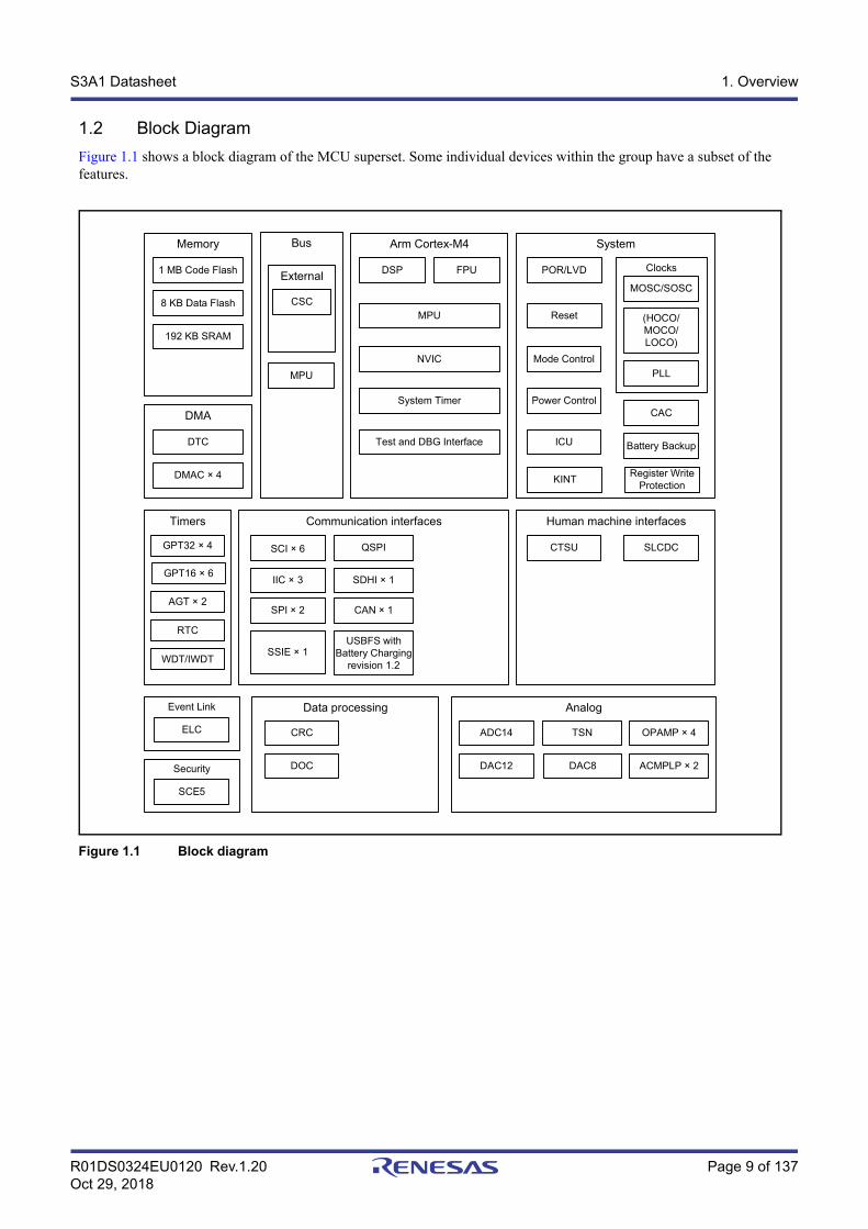
1.2 Block Diagram
Figure 1.1 shows a block diagram of the MCU superset. Some individual devices within the group have a subset of the features.
Figure 1.1 Block diagram
Memory
1 MB Code Flash
8 KB Data Flash
192 KB SRAM
DMA
DMAC × 4
System
Mode Control
Power Control
ICU
MOSC/SOSC
Clocks
(HOCO/MOCO/LOCO)
PLL
Battery Backup
GPT32 × 4
Timers
AGT × 2
RTC
CTSU
Arm Cortex-M4
DSP FPU
MPU
NVIC
System Timer
Test and DBG Interface
Bus
MPU
DTC
CSC
External
WDT/IWDT
CAC
POR/LVD
Reset
Human machine interfaces
SLCDC
ELC
Event Link
SCE5
Security
Analog
CRC
Data processing
DOC
Communication interfaces
QSPI
IIC × 3 SDHI × 1
SPI × 2 CAN × 1
SSIE × 1USBFS with
Battery Charging revision 1.2
SCI × 6
TSN
DAC12 ACMPLP × 2
ADC14 OPAMP × 4
GPT16 × 6
DAC8
KINTRegister Write
Protection
R01DS0324EU0120 Rev.1.20 Page 10 of 137Oct 29, 2018
S3A1 Datasheet 1. Overview
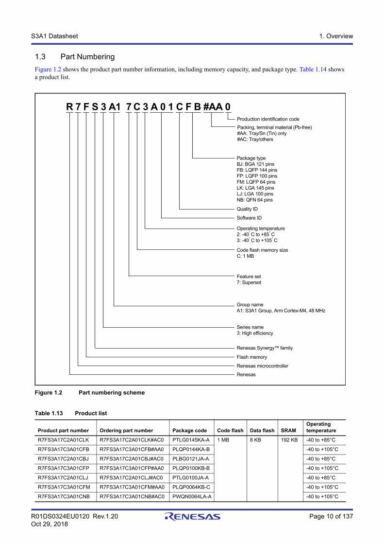
1.3 Part Numbering
Figure 1.2 shows the product part number information, including memory capacity, and package type. Table 1.14 shows a product list.
Figure 1.2 Part numbering scheme
Table 1.13 Product list
Product part number Ordering part number Package code Code flash Data flash SRAMOperating temperature
R7FS3A17C2A01CLK R7FS3A17C2A01CLK#AC0 PTLG0145KA-A 1 MB 8 KB 192 KB -40 to +85°C
R7FS3A17C3A01CFB R7FS3A17C3A01CFB#AA0 PLQP0144KA-B -40 to +105°C
R7FS3A17C2A01CBJ R7FS3A17C2A01CBJ#AC0 PLBG0121JA-A -40 to +85°C
R7FS3A17C3A01CFP R7FS3A17C3A01CFP#AA0 PLQP0100KB-B -40 to +105°C
R7FS3A17C2A01CLJ R7FS3A17C2A01CLJ#AC0 PTLG0100JA-A -40 to +85°C
R7FS3A17C3A01CFM R7FS3A17C3A01CFM#AA0 PLQP0064KB-C -40 to +105°C
R7FS3A17C3A01CNB R7FS3A17C3A01CNB#AC0 PWQN0064LA-A -40 to +105°C
R 7 F S 3 A1 7
Package typeBJ: BGA 121 pinsFB: LQFP 144 pinsFP: LQFP 100 pinsFM: LQFP 64 pinsLK: LGA 145 pinsLJ: LGA 100 pinsNB: QFN 64 pins
Quality ID
Software ID
Operating temperature2: -40° C to +85° C3: -40° C to +105° C
Code flash memory sizeC: 1 MB
Feature set7: Superset
Group nameA1: S3A1 Group, Arm Cortex-M4, 48 MHz
Series name3: High efficiency
Renesas Synergy™ family
Flash memory
Renesas microcontroller
Renesas
C 3 A 0 1 C F B #AA 0Production identification code
Packing, terminal material (Pb-free)#AA: Tray/Sn (Tin) only#AC: Tray/others
R01DS0324EU0120 Rev.1.20 Page 11 of 137Oct 29, 2018
S3A1 Datasheet 1. Overview
1.4 Function Comparison
Table 1.14 Function comparison
Part numbers R7FS3A17C2A01CLK R7FS3A17C3A01CFB R7FS3A17C2A01CBJ R7FS3A17C3A01CFP R7FS3A17C2A01CLJR7FS3A17C3A01CFM/R7FS3A17C3A01CNB
Pin count 145 144 121 100 100 64
Package LGA LQFP BGA LQFP LGA LQFP/QFN
Code flash memory 1 MB
Data flash memory 8 KB
SRAM 192 KB
Parity 176 KB
ECC 16 KB
System CPU clock 48 MHz
Backup registers
512 bytes
ICU Yes
KINT 8
Event control ELC Yes
DMA DTC Yes
DMAC 4
Bus External bus 16-bit bus 8-bit bus No
Timers GPT32 4
GPT16 6
AGT 2
RTC Yes
WDT/IWDT Yes
Communication SCI 6
IIC 3 2
SPI 2
SSIE 1 No
QSPI 1 No
SDHI 1 No
CAN 1
USBFS Yes
Analog ADC14 28 26 25 18
DAC12 1
DAC8 2
ACMPLP 2
OPAMP 4 4 4 4 4 3
TSN Yes
HMI SLCDC 4 com × 54 seg or
8 com x 50 seg
4 com × 46 seg or
8 com x 42 seg
4 com × 38 segor
8 com x 34 seg
4 com × 21 segor
8 com x 17 seg
CTSU 27 24
Data processing
CRC Yes
DOC Yes
Security SCE5
R01DS0324EU0120 Rev.1.20 Page 12 of 137Oct 29, 2018
S3A1 Datasheet 1. Overview
1.5 Pin Functions
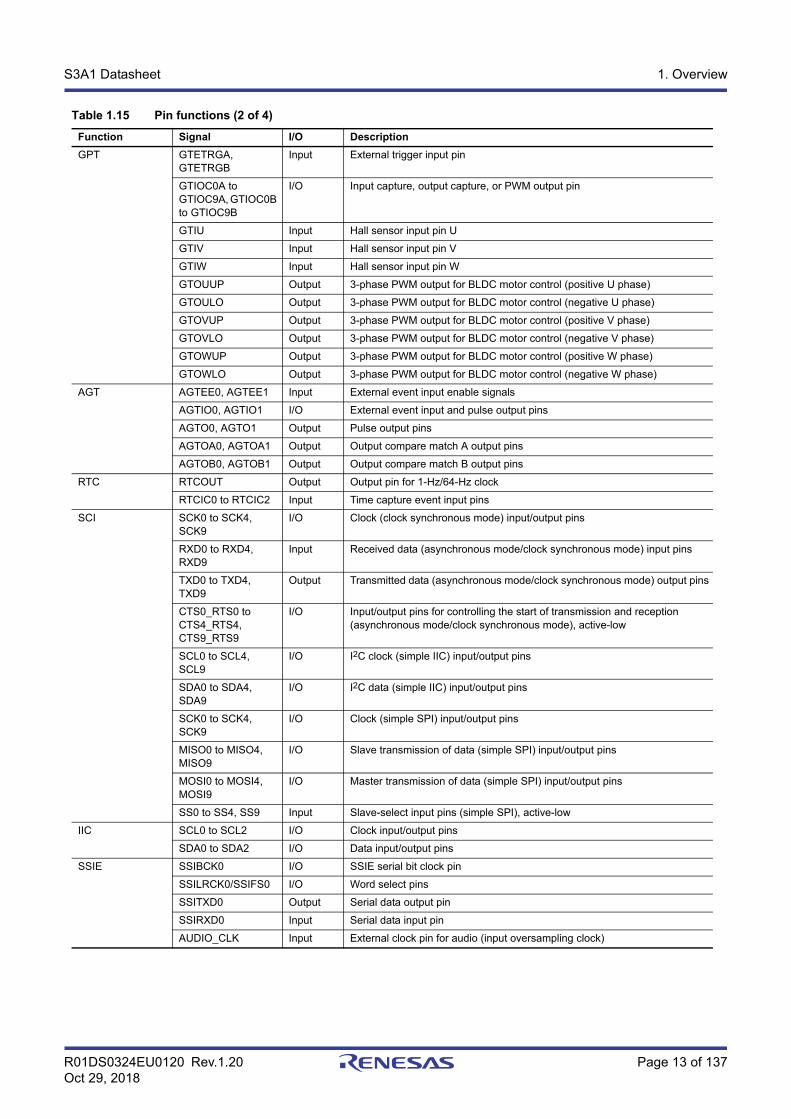
Table 1.15 Pin functions (1 of 4)
Function Signal I/O Description
Power supply VCC Input Power supply pin. Connect this pin to the system power supply. Connect it to VSS through a 0.1-μF capacitor. The capacitor should be placed close to the pin.
VCL Input Connect this pin to the VSS pin through the smoothing capacitor used to stabilize the internal power supply. Place the capacitor close to the pin.
VSS Input Ground pin. Connect to the system power supply (0 V).
VBATT Input Backup power supply pin
Clock XTAL Output Pins for a crystal resonator. An external clock signal can be input through the EXTAL pin.EXTAL Input
XCIN Input Input/output pins for the sub-clock oscillator. Connect a crystal resonator between XCOUT and XCIN.XCOUT Output
EBCLK Output Outputs the external bus clock for external devices
CLKOUT Output Clock output pin
Operating mode control
MD Input Pins for setting the operating mode. The signal levels on these pins must not be changed during operation mode transition on release from the reset state.
System control RES Input Reset signal input pin. The MCU enters the reset state when this signal goes low.
CAC CACREF Input Measurement reference clock input pin
Interrupt NMI Input Non-maskable interrupt request pin
IRQ0 to IRQ15 Input Maskable interrupt request pins
KINT KR00 to KR07 Input Key interrupt input pins.A key interrupt (KINT) can be generated by inputting a falling edge to the key interrupt input pins.
On-chip debug TMS I/O On-chip emulator or boundary scan pins
TDI Input
TCK Input
TDO Output
SWDIO I/O Serial wire debug data input/output pin
SWCLK Input Serial wire clock pin
SWO Output Serial wire trace output pin
External bus interface
RD Output Strobe signal indicating that reading from the external bus interface space is in progress, active-low
WR Output Strobe signal indicating that writing to the external bus interface space is in progress, in 1-write strobe mode, active-low
WR0, WR1 Output Strobe signals indicating that either group of data bus pins (D07 to D00, D15 to D08) is valid in writing to the external bus interface space, in byte strobe mode, active-low
BC0, BC1 Output Strobe signals indicating that either group of data bus pins (D07 to D00, D15 to D08) is valid in access to the external bus interface space, in 1-write strobe mode, active-low
ALE Output Address latch signal when address/data multiplexed bus is selected
WAIT Input Input pin for wait request signals in access to the external space, active-low
CS0 to CS3 Output Select signals for CS areas, active-low
A00 to A23 Output Address bus
D00 to D15 I/O Data bus
Battery backup VBATWIO0 to VBATWIO2
I/O Output wakeup signal for the VBATT wakeup control function.External event input for the VBATT wakeup control function.
R01DS0324EU0120 Rev.1.20 Page 13 of 137Oct 29, 2018
S3A1 Datasheet 1. Overview
GPT GTETRGA, GTETRGB
Input External trigger input pin
GTIOC0A to GTIOC9A, GTIOC0B to GTIOC9B
I/O Input capture, output capture, or PWM output pin
GTIU Input Hall sensor input pin U
GTIV Input Hall sensor input pin V
GTIW Input Hall sensor input pin W
GTOUUP Output 3-phase PWM output for BLDC motor control (positive U phase)
GTOULO Output 3-phase PWM output for BLDC motor control (negative U phase)
GTOVUP Output 3-phase PWM output for BLDC motor control (positive V phase)
GTOVLO Output 3-phase PWM output for BLDC motor control (negative V phase)
GTOWUP Output 3-phase PWM output for BLDC motor control (positive W phase)
GTOWLO Output 3-phase PWM output for BLDC motor control (negative W phase)
AGT AGTEE0, AGTEE1 Input External event input enable signals
AGTIO0, AGTIO1 I/O External event input and pulse output pins
AGTO0, AGTO1 Output Pulse output pins
AGTOA0, AGTOA1 Output Output compare match A output pins
AGTOB0, AGTOB1 Output Output compare match B output pins
RTC RTCOUT Output Output pin for 1-Hz/64-Hz clock
RTCIC0 to RTCIC2 Input Time capture event input pins
SCI SCK0 to SCK4, SCK9
I/O Clock (clock synchronous mode) input/output pins
RXD0 to RXD4, RXD9
Input Received data (asynchronous mode/clock synchronous mode) input pins
TXD0 to TXD4, TXD9
Output Transmitted data (asynchronous mode/clock synchronous mode) output pins
CTS0_RTS0 to CTS4_RTS4, CTS9_RTS9
I/O Input/output pins for controlling the start of transmission and reception (asynchronous mode/clock synchronous mode), active-low
SCL0 to SCL4, SCL9
I/O I2C clock (simple IIC) input/output pins
SDA0 to SDA4, SDA9
I/O I2C data (simple IIC) input/output pins
SCK0 to SCK4, SCK9
I/O Clock (simple SPI) input/output pins
MISO0 to MISO4, MISO9
I/O Slave transmission of data (simple SPI) input/output pins
MOSI0 to MOSI4, MOSI9
I/O Master transmission of data (simple SPI) input/output pins
SS0 to SS4, SS9 Input Slave-select input pins (simple SPI), active-low
IIC SCL0 to SCL2 I/O Clock input/output pins
SDA0 to SDA2 I/O Data input/output pins
SSIE SSIBCK0 I/O SSIE serial bit clock pin
SSILRCK0/SSIFS0 I/O Word select pins
SSITXD0 Output Serial data output pin
SSIRXD0 Input Serial data input pin
AUDIO_CLK Input External clock pin for audio (input oversampling clock)
Table 1.15 Pin functions (2 of 4)
Function Signal I/O Description
R01DS0324EU0120 Rev.1.20 Page 14 of 137Oct 29, 2018
S3A1 Datasheet 1. Overview
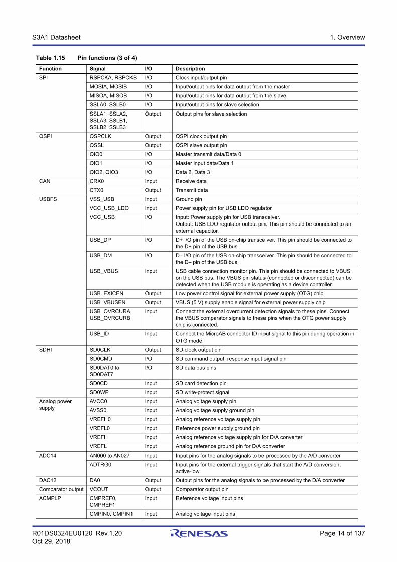
SPI RSPCKA, RSPCKB I/O Clock input/output pin
MOSIA, MOSIB I/O Input/output pins for data output from the master
MISOA, MISOB I/O Input/output pins for data output from the slave
SSLA0, SSLB0 I/O Input/output pins for slave selection
SSLA1, SSLA2, SSLA3, SSLB1, SSLB2, SSLB3
Output Output pins for slave selection
QSPI QSPCLK Output QSPI clock output pin
QSSL Output QSPI slave output pin
QIO0 I/O Master transmit data/Data 0
QIO1 I/O Master input data/Data 1
QIO2, QIO3 I/O Data 2, Data 3
CAN CRX0 Input Receive data
CTX0 Output Transmit data
USBFS VSS_USB Input Ground pin
VCC_USB_LDO Input Power supply pin for USB LDO regulator
VCC_USB I/O Input: Power supply pin for USB transceiver.Output: USB LDO regulator output pin. This pin should be connected to an external capacitor.
USB_DP I/O D+ I/O pin of the USB on-chip transceiver. This pin should be connected to the D+ pin of the USB bus.
USB_DM I/O D– I/O pin of the USB on-chip transceiver. This pin should be connected to the D– pin of the USB bus.
USB_VBUS Input USB cable connection monitor pin. This pin should be connected to VBUS on the USB bus. The VBUS pin status (connected or disconnected) can be detected when the USB module is operating as a device controller.
USB_EXICEN Output Low power control signal for external power supply (OTG) chip
USB_VBUSEN Output VBUS (5 V) supply enable signal for external power supply chip
USB_OVRCURA, USB_OVRCURB
Input Connect the external overcurrent detection signals to these pins. Connect the VBUS comparator signals to these pins when the OTG power supply chip is connected.
USB_ID Input Connect the MicroAB connector ID input signal to this pin during operation in OTG mode
SDHI SD0CLK Output SD clock output pin
SD0CMD I/O SD command output, response input signal pin
SD0DAT0 to SD0DAT7
I/O SD data bus pins
SD0CD Input SD card detection pin
SD0WP Input SD write-protect signal
Analog power supply
AVCC0 Input Analog voltage supply pin
AVSS0 Input Analog voltage supply ground pin
VREFH0 Input Analog reference voltage supply pin
VREFL0 Input Reference power supply ground pin
VREFH Input Analog reference voltage supply pin for D/A converter
VREFL Input Analog reference ground pin for D/A converter
ADC14 AN000 to AN027 Input Input pins for the analog signals to be processed by the A/D converter
ADTRG0 Input Input pins for the external trigger signals that start the A/D conversion, active-low
DAC12 DA0 Output Output pins for the analog signals to be processed by the D/A converter
Comparator output VCOUT Output Comparator output pin
ACMPLP CMPREF0, CMPREF1
Input Reference voltage input pins
CMPIN0, CMPIN1 Input Analog voltage input pins
Table 1.15 Pin functions (3 of 4)
Function Signal I/O Description
R01DS0324EU0120 Rev.1.20 Page 15 of 137Oct 29, 2018
S3A1 Datasheet 1. Overview
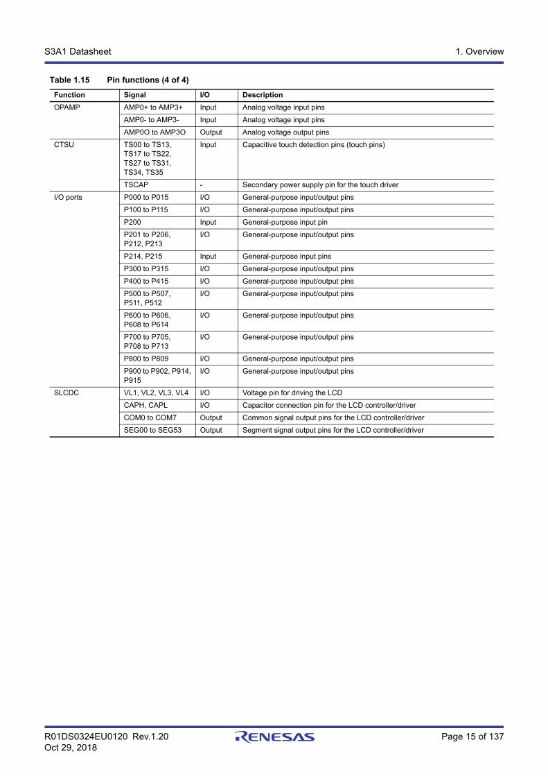
OPAMP AMP0+ to AMP3+ Input Analog voltage input pins
AMP0- to AMP3- Input Analog voltage input pins
AMP0O to AMP3O Output Analog voltage output pins
CTSU TS00 to TS13, TS17 to TS22, TS27 to TS31, TS34, TS35
Input Capacitive touch detection pins (touch pins)
TSCAP - Secondary power supply pin for the touch driver
I/O ports P000 to P015 I/O General-purpose input/output pins
P100 to P115 I/O General-purpose input/output pins
P200 Input General-purpose input pin
P201 to P206, P212, P213
I/O General-purpose input/output pins
P214, P215 Input General-purpose input pins
P300 to P315 I/O General-purpose input/output pins
P400 to P415 I/O General-purpose input/output pins
P500 to P507, P511, P512
I/O General-purpose input/output pins
P600 to P606, P608 to P614
I/O General-purpose input/output pins
P700 to P705, P708 to P713
I/O General-purpose input/output pins
P800 to P809 I/O General-purpose input/output pins
P900 to P902, P914, P915
I/O General-purpose input/output pins
SLCDC VL1, VL2, VL3, VL4 I/O Voltage pin for driving the LCD
CAPH, CAPL I/O Capacitor connection pin for the LCD controller/driver
COM0 to COM7 Output Common signal output pins for the LCD controller/driver
SEG00 to SEG53 Output Segment signal output pins for the LCD controller/driver
Table 1.15 Pin functions (4 of 4)
Function Signal I/O Description
R01DS0324EU0120 Rev.1.20 Page 16 of 137Oct 29, 2018
S3A1 Datasheet 1. Overview
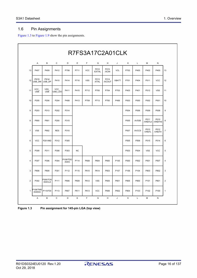
1.6 Pin Assignments
Figure 1.3 to Figure 1.9 show the pin assignments.
Figure 1.3 Pin assignment for 145-pin LGA (top view)
P400
VCC
VSS
P001
P008
P010/VREFH0
P012/VREFH
P014
VCC
P507
P802
P801
P100
P402
P511
P512
P002
P009
P011/VREFL0
P013/VREFL
P015
VSS
P501
P803
P101
P102
P405
P404
P401
P000
P006
AVSS0
AVCC0
P506
P504
P502
P104
P800
P103
P702
P701
P403
P003
P004
P005
P007
P505
P503
P500
P106
P805
P804
VCL
VBATT
P703
P406
P105
P107
P601
P602
P215/XCIN
P214/XCOUT
P704
P700
P600
P603
P605
P606
P212/EXTAL
P213/XTAL
P705
P713
P604
P614
VSS
VCC
VCC
VSS
P712
P709
P608
P610
P612
P613
P711
P710
P415
P413
P114
P115
P609
P611
P708
P414
P411
P408
P314
P315
P310
P305
P303
P109/TDO/SWO
P112
P806
P807
P412
P410
VCC_USB_LDO
P204
P202
P200
RES
P312
P308
P304
P301
P111
P113
P409
P914/USB_DP
VSS_USB
P206
P313
P901
P902
P201/MD
P311
P306
P809
P300/TCK/SWCLK
P110/TDI
P407
P915/USB_DM
VCC_USB
P205
P203
P900
VSS
VCC
P309
P307
P808
P302
P108/TMS/SWDIO
R7FS3A17C2A01CLK
13
12
11
10
9
8
7
6
5
4
3
2
1
13
12
11
10
9
8
7
6
5
4
3
2
1
N K L MG H JD E FA B C
N K L MG H JD E FA B C
NC
R01DS0324EU0120 Rev.1.20 Page 17 of 137Oct 29, 2018
S3A1 Datasheet 1. Overview
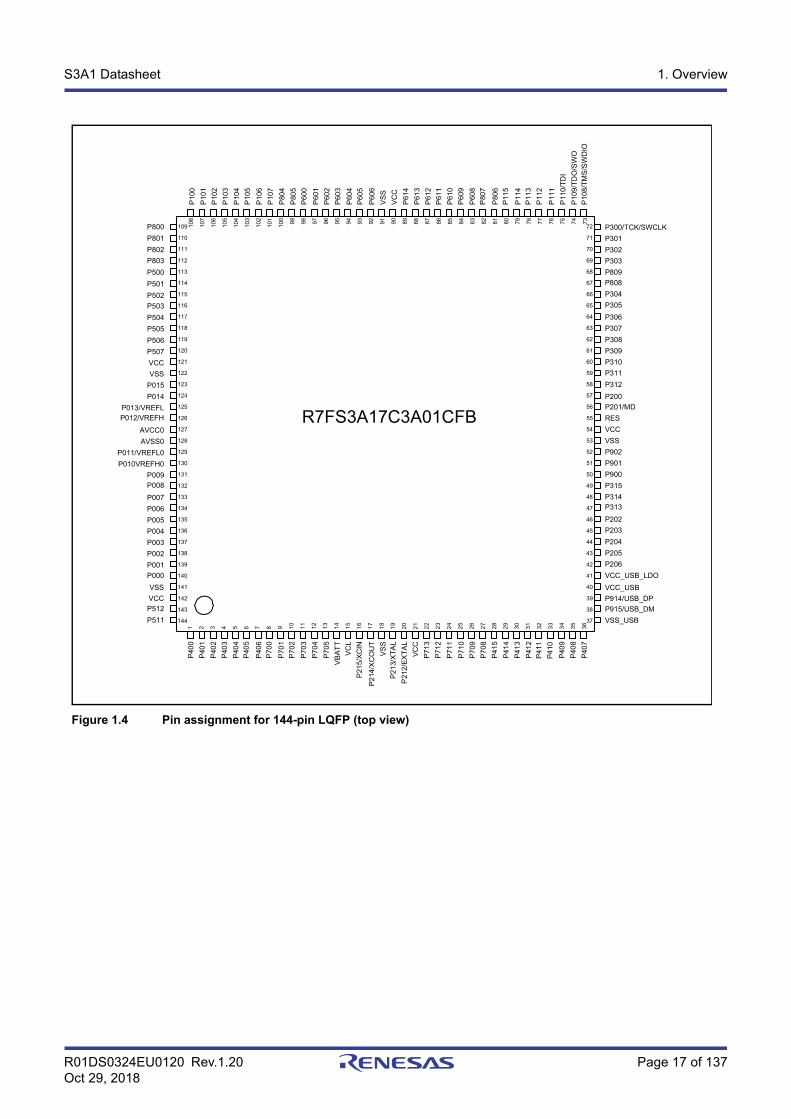
Figure 1.4 Pin assignment for 144-pin LQFP (top view)
1 2 3 4 5 6 7 8 9 10
11
12
13
14
15
16
17
18
19
20
21
22
23
24
25
26
27
28
29
30
31
32
33
34
35
36
108
107
106
105
104
103
102
101
100 99 98 97 96 95 94 93 92 91 90 89 88 87 86 85 84 83 82 81 80 79 78 77 76 75 74 73
72
71
70
69
68
67
66
65
64
63
62
61
60
59
58
57
56
55
54
53
52
51
50
49
48
47
46
45
44
43
42
41
40
39
38
37
109
110
111
112
113
114
115
116
117
118
119
120
121
122
123
124
125
126
127
128
129
130
131
132
133
134
135
136
137
138
139
140
141
142
143
144
P802
P803
P500
P501
P502
P503
P504
P505
P506
P507
VCC
VSS
P014
P013/VREFLP012/VREFH
AVCC0
AVSS0
P011/VREFL0
P010VREFH0
P009
P008
P007
P006
P005
P004
P003
P002
P001
P000
VSS
VCC
P511
P801
P015
P512
P300/TCK/SWCLK
P302
P303
P809
P808
P304
P305
P306
P307
P308
P309
P310
P311
P200
P201/MD
RES
VCC
VSS
P902
P901
P900
P315
P314P313
P202
P203
P204
P205
P206
VCC_USB_LDO
VCC_USB
P914/USB_DP
VSS_USB
P301
P312
P915/USB_DM
P10
0
P10
2
P10
3
P10
4
P10
5
P10
6
P10
7
P80
4
P80
5
P60
0
P60
1
P60
2
P60
3
P60
5
P60
6
VS
S
VC
C
P61
4
P61
3
P61
2
P61
1
P61
0
P60
9
P60
8
P80
7
P80
6
P11
5
P11
4
P11
3
P11
2
P11
1
P11
0/T
DI
P10
8/T
MS
/SW
DIO
P10
1
P60
4
P10
9/T
DO
/SW
O
P40
0
P40
2
P40
3
P40
4
P40
5
P40
6
P70
0
P70
1
P70
2
P70
3
P70
4
P70
5
VB
AT
T
P21
5/X
CIN
P2
14/X
CO
UT
VS
SP
213/
XT
AL
P21
2/E
XT
AL
VC
C
P71
3
P71
2
P71
1
P71
0
P70
8
P41
5
P41
4
P41
3
P41
2
P41
1
P4
10
P40
9
P40
7
P40
1
VC
L
P40
8
P70
9
P800
R7FS3A17C3A01CFB
R01DS0324EU0120 Rev.1.20 Page 18 of 137Oct 29, 2018
S3A1 Datasheet 1. Overview
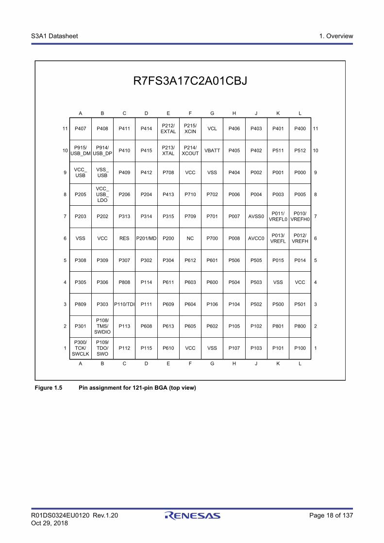
Figure 1.5 Pin assignment for 121-pin BGA (top view)
R7FS3A17C2A01CBJ
11
10
9
8
7
6
5
4
3
2
1
11
10
9
8
7
6
5
4
3
2
1
A B C D E F G H J K L
A B C D E F G H J K L
P407
P915/USB_DM
VCC_USB
P205
P203
VSS
P308
P305
P809
P301
P300/TCK/
SWCLK
P408 P411 P414P212/
EXTALP215/XCIN
VCL P406 P403 P401 P400
P914/USB_DP
P410 P415P213/XTAL
P214/XCOUT
VBATT P405 P402 P511 P512
VSS_USB
P409 P412 P708 VCC VSS P404 P002 P001 P000
VCC_USB_LDO
P206 P204 P413 P710 P702 P006 P004 P003 P005
VCC RES P201/MD P200 NC P700 P008 AVCC0P013/
VREFLP012/
VREFH
P309 P307 P302 P304 P612 P601 P506 P505 P015 P014
P306 P808 P114 P611 P603 P600 P504 P503 VSS VCC
P303 P110/TDI P111 P609 P604 P106 P104 P502 P500 P501
P108/TMS/
SWDIOP113 P608 P613 P605 P602 P105 P102 P801 P800
P202 P313 P314 P315 P709 P701 P007 AVSS0P011/
VREFL0P010/
VREFH0
P109/TDO/SWO
P112 P115 P610 VCC VSS P107 P103 P101 P100
R01DS0324EU0120 Rev.1.20 Page 19 of 137Oct 29, 2018
S3A1 Datasheet 1. Overview
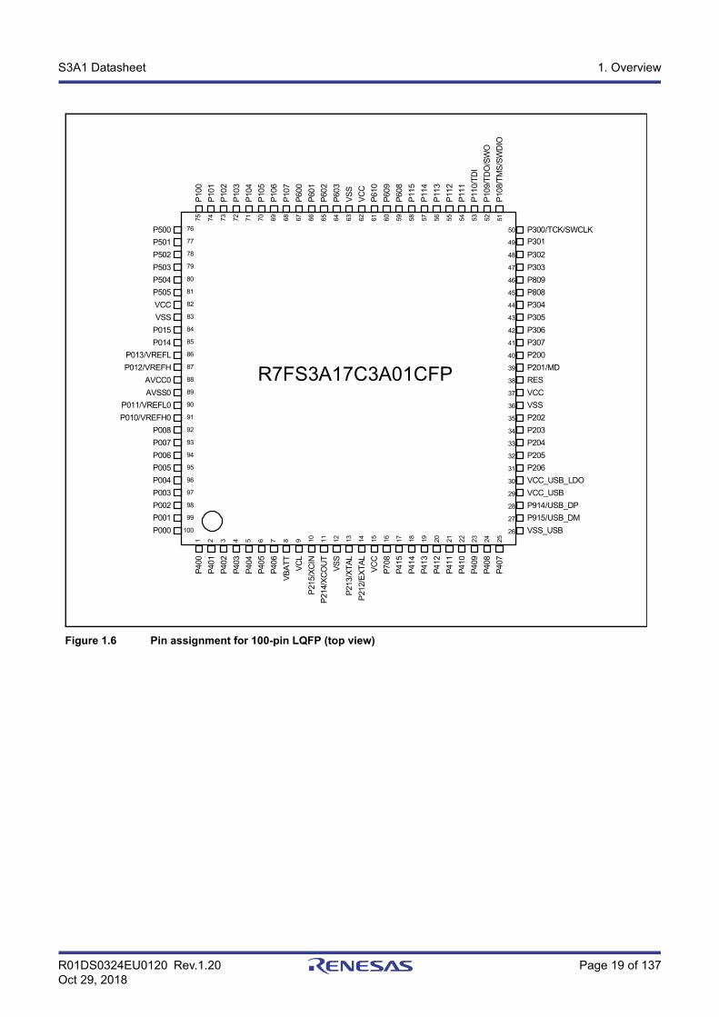
Figure 1.6 Pin assignment for 100-pin LQFP (top view)
1 2 3 4 5 6 7 8 9 10 11 12 13 14 15 16 17 18 19 20 21 22 23 24 25
75 74 73 72 71 70 69 68 67 66 65 64 63 62 61 60 59 58 57 56 55 54 53 52 51
50
49
48
47
46
45
44
43
42
41
40
39
38
37
36
35
34
33
32
31
30
29
28
27
26
76
77
78
79
80
81
82
83
84
85
86
87
88
89
90
91
92
93
94
95
96
97
98
99
100
P502
P503
P504
P505
VCC
VSS
P015
P014
P013/VREFL
P012/VREFH
AVCC0
AVSS0
P010/VREFH0
P008
P007
P006
P005
P004
P003
P002
P001
P501
P011/VREFL0
P300/TCK/SWCLK
P302
P303
P809
P808
P304
P305
P306
P307
P200
P201/MD
RES
VCC
P202
P203
P204
P205
P206
VCC_USB_LDO
VCC_USB
P914/USB_DP
P915/USB_DM
VSS_USB
P301
VSS
P10
0
P10
2
P10
3
P10
4
P10
5
P10
6
P10
7
P60
0
P60
1
P60
2
P60
3
VS
S
VC
C
P60
9
P60
8
P11
5
P11
4
P11
3
P11
2
P11
1
P11
0/T
DI
P10
9/T
DO
/SW
O
P10
8/T
MS
/SW
DIO
P10
1
P61
0
P40
0
P40
2
P40
3
P40
4
P40
5
P40
6
VB
AT
T
VC
L
P21
5/X
CIN
P21
4/X
CO
UT
VS
S
P21
3/X
TA
L
VC
C
P70
8
P41
5
P41
4
P41
3
P41
2
P41
1
P41
0
P40
9
P40
7
P40
1
P21
2/E
XT
AL
P500
P000
P40
8
R7FS3A17C3A01CFP
R01DS0324EU0120 Rev.1.20 Page 20 of 137Oct 29, 2018
S3A1 Datasheet 1. Overview
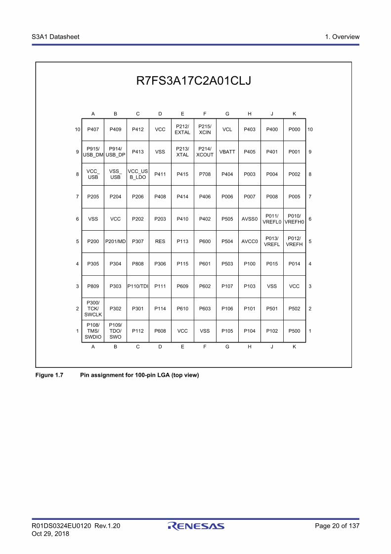
Figure 1.7 Pin assignment for 100-pin LGA (top view)
R7FS3A17C2A01CLJ
P407
P915/USB_DM
VCC_USB
P205
VSS
P200
P305
P809
P300/TCK/
SWCLK
P108/TMS/
SWDIO
P409 P412 VCCP212/
EXTALP215/XCIN
VCL P403 P400 P000
P914/USB_DP
P413 VSSP213/XTAL
P214/XCOUT
VBATT P405 P401 P001
VSS_USB
VCC_USB_LDO
P411 P415 P708 P404 P003 P004 P002
P204 P206 P408 P414 P406 P006 P007 P008 P005
P201/MD P307 RES P113 P600 P504 AVCC0P013/
VREFLP012/
VREFH
P304 P808 P306 P115 P601 P503 P100 P015 P014
P303 P110/TDI P111 P609 P602 P107 P103 VSS VCC
P302 P301 P114 P610 P603 P106 P101 P501 P502
P109/TDO/SWO
P112 P608 VCC VSS P105 P104 P102 P500
VCC P202 P203 P410 P402 P505 AVSS0P011/
VREFL0P010/
VREFH0
10
9
8
7
6
5
4
3
2
1
10
9
8
7
6
5
4
3
2
1
A B C D E F G H J K
A B C D E F G H J K
R01DS0324EU0120 Rev.1.20 Page 21 of 137Oct 29, 2018
S3A1 Datasheet 1. Overview
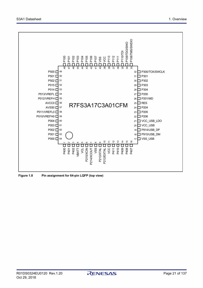
Figure 1.8 Pin assignment for 64-pin LQFP (top view)
1 2 3 4 5 6 7 8 9 10 11 12 13 14 15 16
48 47 46 45 44 43 42 41 40 39 38 37 36 35 34 33
32
31
30
29
28
27
26
25
24
23
22
21
20
19
18
17
49
50
51
52
53
54
55
56
57
58
59
60
61
62
63
64
P501
P502
P015
P014
P012/VREFH
AVCC0
AVSS0
P011/VREFL0
P010/VREFH0
P004
P003
P002
P001
P013/VREFL
P300/TCK/SWCLK
P301
P302
P303
P304
P201/MD
RES
P204
P205
P206
VCC_USB_LDO
VCC_USB
P914/USB_DP
P915/USB_DM
VSS_USB
P200
P10
0
P10
2
P10
3
P10
4
P10
5
P10
6
P10
7
VS
S
VC
C
P11
3
P11
2
P11
1
P11
0/T
DI
P10
8/T
MS
/SW
DIO
P10
1
P10
9/T
DO
/SW
O
P40
0
P40
2
VB
AT
T
VC
L
P21
5/X
CIN
P21
4/X
CO
UT
VS
S
P21
3/X
TA
L
P21
2/E
XT
AL
VC
C
P41
1
P41
0
P40
8
P40
7
P40
1
P40
9
P000
R7FS3A17C3A01CFM
P500
R01DS0324EU0120 Rev.1.20 Page 22 of 137Oct 29, 2018
S3A1 Datasheet 1. Overview
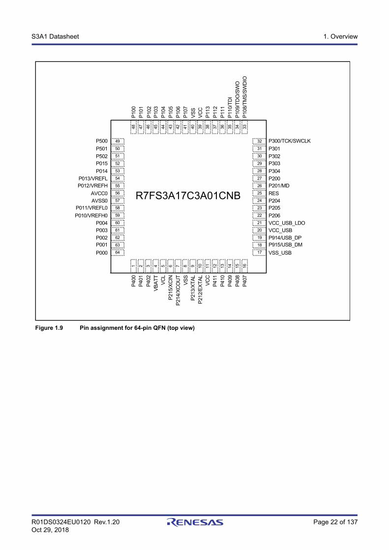
Figure 1.9 Pin assignment for 64-pin QFN (top view)
P300/TCK/SWCLK
P301
P302P303
P304
P201/MD
RES
P204P205
P206
VCC_USB_LDO
VCC_USB
P914/USB_DPP915/USB_DM
VSS_USB
P200
P10
0
P10
2P
103
P10
4
P10
5
P10
6
P10
7
VS
SV
CC
P11
3
P11
2
P11
1
P11
0/T
DI
P10
8/T
MS
/SW
DIO
P10
1
P10
9/T
DO
/SW
O
P40
0
P40
2
VB
AT
TV
CL
P21
5/X
CIN
P21
4/X
CO
UT
VS
SP
213/
XT
AL
P21
2/E
XT
AL
VC
C
P41
1
P41
0
P40
8
P40
7
P40
1
P40
9
R7FS3A17C3A01CNB
17
18
19
20
21
22
23
24
25
26
27
28
29
30
31
32
33343536373839404142434445464748
16151413121110987654321
64
63
62
61
60
59
58
57
56
55
54
53
52
51
50
49P500
P501
P502P015
P014
P012/VREFH
AVCC0
AVSS0P011/VREFL0
P010/VREFH0
P004
P003
P002P001
P000
P013/VREFL
R01DS0324EU0120 Rev.1.20 Page 23 of 137Oct 29, 2018
S3A1 Datasheet 1. Overview
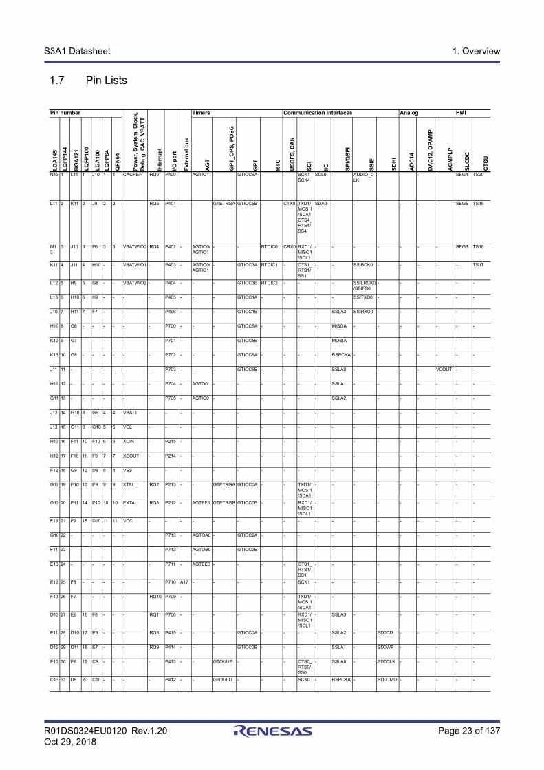
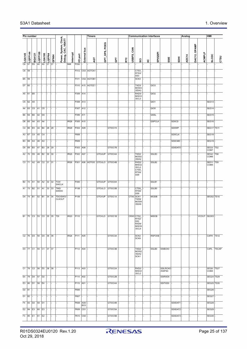
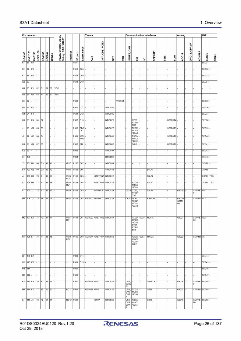
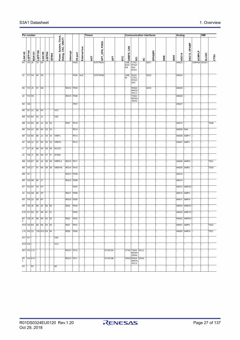
1.7 Pin Lists
Pin number
Po
wer
, S
yste
m,
Clo
ck,
Deb
ug
, CA
C, V
BA
TT
Inte
rru
pt
I/O
po
rt
Ext
ern
al b
us
Timers Communication interfaces Analog HMI
LG
A1
45
LQ
FP
144
BG
A12
1
LQ
FP
100
LG
A1
00
LQ
FP
64
QF
N64
AG
T
GP
T_O
PS
, PO
EG
GP
T
RT
C
US
BF
S, C
AN
SC
I
IIC
SP
I/QS
PI
SS
IE
SD
HI
AD
C14
DA
C12
, OP
AM
P
AC
MP
LP
SL
CD
C
CT
SU
N13 1 L11 1 J10 1 1 CACREF IRQ0 P400 - AGTIO1 - GTIOC6A - - SCK1SCK4
SCL0 - AUDIO_CLK
- - - - SEG4 TS20
L11 2 K11 2 J9 2 2 - IRQ5 P401 - - GTETRGA GTIOC6B - CTX0 TXD1/MOSI1/SDA1CTS4_RTS4/SS4
SDA0 - - - - - - SEG5 TS19
M13
3 J10 3 F6 3 3 VBATWIO0 IRQ4 P402 - AGTIO0/AGTIO1
- - RTCIC0 CRX0 RXD1/MISO1/SCL1
- - - - - - - SEG6 TS18
K11 4 J11 4 H10 - - VBATWIO1 - P403 - AGTIO0/AGTIO1
- GTIOC3A RTCIC1 - CTS1_RTS1/SS1
- - SSIBCK0 - - - - - TS17
L12 5 H9 5 G8 - - VBATWIO2 - P404 - - - GTIOC3B RTCIC2 - - - - SSILRCK0/SSIFS0
- - - - - -
L13 6 H10 6 H9 - - - - P405 - - - GTIOC1A - - - - - SSITXD0 - - - - - -
J10 7 H11 7 F7 - - - - P406 - - - GTIOC1B - - - - SSLA3 SSIRXD0 - - - - - -
H10 8 G6 - - - - - - P700 - - - GTIOC5A - - - - MISOA - - - - - - -
K12 9 G7 - - - - - - P701 - - - GTIOC5B - - - - MOSIA - - - - - - -
K13 10 G8 - - - - - - P702 - - - GTIOC6A - - - - RSPCKA - - - - - - -
J11 11 - - - - - - - P703 - - - GTIOC6B - - - - SSLA0 - - - - VCOUT - -
H11 12 - - - - - - - P704 - AGTO0 - - - - - - SSLA1 - - - - - - -
G11 13 - - - - - - - P705 - AGTIO0 - - - - - - SSLA2 - - - - - - -
J12 14 G10 8 G9 4 4 VBATT - - - - - - - - - - - - - - - - - -
J13 15 G11 9 G10 5 5 VCL - - - - - - - - - - - - - - - - - -
H13 16 F11 10 F10 6 6 XCIN - P215 - - - - - - - - - - - - - - - -
H12 17 F10 11 F9 7 7 XCOUT - P214 - - - - - - - - - - - - - - - -
F12 18 G9 12 D9 8 8 VSS - - - - - - - - - - - - - - - - - -
G12 19 E10 13 E9 9 9 XTAL IRQ2 P213 - - GTETRGA GTIOC0A - - TXD1/MOSI1/SDA1
- - - - - - - - -
G13 20 E11 14 E10 10 10 EXTAL IRQ3 P212 - AGTEE1 GTETRGB GTIOC0B - - RXD1/MISO1/SCL1
- - - - - - - - -
F13 21 F9 15 D10 11 11 VCC - - - - - - - - - - - - - - - - - -
G10 22 - - - - - - - P713 - AGTOA0 - GTIOC2A - - - - - - - - - - - -
F11 23 - - - - - - - P712 - AGTOB0 - GTIOC2B - - - - - - - - - - - -
E13 24 - - - - - - - P711 - AGTEE0 - - - - CTS1_RTS1/SS1
- - - - - - - - -
E12 25 F8 - - - - - - P710 A17 - - - - - SCK1 - - - - - - - - -
F10 26 F7 - - - - - IRQ10 P709 - - - - - - TXD1/MOSI1/SDA1
- - - - - - - - -
D13 27 E9 16 F8 - - - IRQ11 P708 - - - - - - RXD1/MISO1/SCL1
- SSLA3 - - - - - - -
E11 28 D10 17 E8 - - - IRQ8 P415 - - - GTIOC0A - - - - SSLA2 - SD0CD - - - - -
D12 29 D11 18 E7 - - - IRQ9 P414 - - - GTIOC0B - - - - SSLA1 - SD0WP - - - - -
E10 30 E8 19 C9 - - - - P413 - - GTOUUP - - - CTS0_RTS0/SS0
- SSLA0 - SD0CLK - - - - -
C13 31 D9 20 C10 - - - - P412 - - GTOULO - - - SCK0 - RSPCKA - SD0CMD - - - - -
R01DS0324EU0120 Rev.1.20 Page 24 of 137Oct 29, 2018
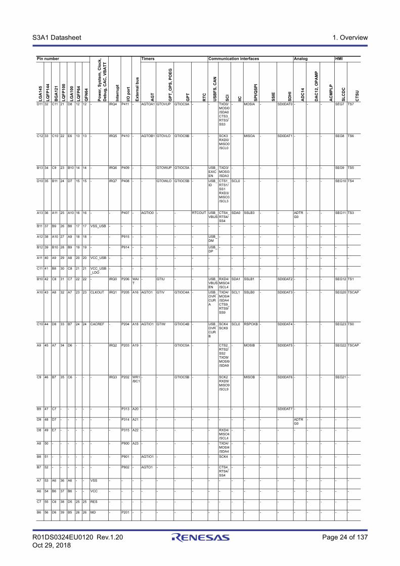
S3A1 Datasheet 1. Overview
D11 32 C11 21 D8 12 12 - IRQ4 P411 - AGTOA1 GTOVUP GTIOC9A - - TXD0/MOSI0/SDA0CTS3_RTS3/SS3
- MOSIA - SD0DAT0 - - - SEG7 TS7
C12 33 C10 22 E6 13 13 - IRQ5 P410 - AGTOB1 GTOVLO GTIOC9B - - SCK3RXD0/MISO0/SCL0
- MISOA - SD0DAT1 - - - SEG8 TS6
B13 34 C9 23 B10 14 14 - IRQ6 P409 - - GTOWUP GTIOC5A - USB_EXICEN
TXD3/MOSI3/SDA3
- - - - - - - SEG9 TS5
D10 35 B11 24 D7 15 15 - IRQ7 P408 - - GTOWLO GTIOC5B - USB_ID
CTS1_RTS1/SS1RXD3/MISO3/SCL3
SCL0 - - - - - - SEG10 TS4
A13 36 A11 25 A10 16 16 - - P407 - AGTIO0 - - RTCOUT USB_VBUS
CTS4_RTS4/SS4
SDA0 SSLB3 - - ADTRG0
- - SEG11 TS3
B11 37 B9 26 B8 17 17 VSS_USB - - - - - - - - - - - - - - - - - -
A12 38 A10 27 A9 18 18 - - P915 - - - - - USB_DM
- - - - - - - - - -
B12 39 B10 28 B9 19 19 - - P914 - - - - - USB_DP
- - - - - - - - - -
A11 40 A9 29 A8 20 20 VCC_USB - - - - - - - - - - - - - - - - - -
C11 41 B8 30 C8 21 21 VCC_USB_LDO
- - - - - - - - - - - - - - - - - -
B10 42 C8 31 C7 22 22 - IRQ0 P206 WAIT
- GTIU - - USB_VBUSEN
RXD4/MISO4/SCL4
SDA1 SSLB1 - SD0DAT2 - - - SEG12 TS1
A10 43 A8 32 A7 23 23 CLKOUT IRQ1 P205 A16 AGTO1 GTIV GTIOC4A - USB_OVRCURA
TXD4/MOSI4/SDA4CTS9_RTS9/SS9
SCL1 SSLB0 - SD0DAT3 - - - SEG20 TSCAP
C10 44 D8 33 B7 24 24 CACREF - P204 A18 AGTIO1 GTIW GTIOC4B - USB_OVRCURB
SCK4SCK9
SCL0 RSPCKB - SD0DAT4 - - - SEG23 TS0
A9 45 A7 34 D6 - - - IRQ2 P203 A19 - - GTIOC5A - - CTS2_RTS2/SS2TXD9/MOSI9/SDA9
- MOSIB - SD0DAT5 - - - SEG22 TSCAP
C9 46 B7 35 C6 - - - IRQ3 P202 WR1/BC1
- - GTIOC5B - - SCK2RXD9/MISO9/SCL9
- MISOB - SD0DAT6 - - - SEG21 -
B9 47 C7 - - - - - - P313 A20 - - - - - - - - - SD0DAT7 - - - - -
D9 48 D7 - - - - - - P314 A21 - - - - - - - - - - ADTRG0
- - - -
D8 49 E7 - - - - - - P315 A22 - - - - - RXD4/MISO4/SCL4
- - - - - - - - -
A8 50 - - - - - - - P900 A23 - - - - - TXD4/MOSI4/SDA4
- - - - - - - - -
B8 51 - - - - - - - P901 - AGTIO1 - - - - SCK4 - - - - - - - - -
B7 52 - - - - - - - P902 - AGTO1 - - - - CTS4_RTS4/SS4
- - - - - - - - -
A7 53 A6 36 A6 - - VSS - - - - - - - - - - - - - - - - - -
A6 54 B6 37 B6 - - VCC - - - - - - - - - - - - - - - - - -
C7 55 C6 38 D5 25 25 RES - - - - - - - - - - - - - - - - - -
B6 56 D6 39 B5 26 26 MD - P201 - - - - - - - - - - - - - - - -
Pin number
Po
we
r, S
yste
m,
Clo
ck,
D
ebu
g, C
AC
, VB
AT
T
Inte
rru
pt
I/O
po
rt
Ext
ern
al b
us
Timers Communication interfaces Analog HMI
LG
A1
45
LQ
FP
144
BG
A12
1
LQ
FP
100
LG
A1
00
LQ
FP
64
QF
N64
AG
T
GP
T_
OP
S, P
OE
G
GP
T
RT
C
US
BF
S, C
AN
SC
I
IIC
SP
I/QS
PI
SS
IE
SD
HI
AD
C1
4
DA
C1
2, O
PA
MP
AC
MP
LP
SL
CD
C
CT
SU
R01DS0324EU0120 Rev.1.20 Page 25 of 137Oct 29, 2018
S3A1 Datasheet 1. Overview
C8 57 E6 40 A5 27 27 - NMI P200 - - - - - - - - - - - - - - - -
C6 58 - - - - - - - P312 CS3 AGTOA1 - - - - CTS3_RTS3/SS3
- - - - - - - - -
B5 59 - - - - - - - P311 CS2 AGTOB1 - - - - SCK3 - - - - - - - - -
D7 60 - - - - - - - P310 A15 AGTEE1 - - - - TXD3/MOSI3/SDA3
- QIO3 - - - - - - -
A5 61 B5 - - - - - - P309 A14 - - - - - RXD3/MISO3/SCL3
- QIO2 - - - - - - -
C5 62 A5 - - - - - - P308 A13 - - - - - - - QIO1 - - - - - SEG13 -
A4 63 C5 41 C5 - - - - P307 A12 - - - - - - - QIO0 - - - - - SEG14 -
B4 64 B4 42 D4 - - - - P306 A11 - - - - - - - QSSL - - - - - SEG15 -
D6 65 A4 43 A4 - - - IRQ8 P305 A10 - - - - - - - QSPCLK - SD0CD - - - SEG16 -
C4 66 E5 44 B4 28 28 - IRQ9 P304 A09 - - GTIOC7A - - - - - - SD0WP - - - SEG17 TS11
A3 67 C4 45 C4 - - - - P808 - - - - - - - - - - SD0CLK - - - SEG18 -
B3 68 A3 46 A3 - - - - P809 - - - - - - - - - - SD0CMD - - - SEG19 -
D5 69 B3 47 B3 29 29 - - P303 A08 - - GTIOC7B - - - - - - SD0DAT0 - - - SEG3/COM7
TS2
A2 70 D5 48 B2 30 30 - IRQ5 P302 A07 - GTOUUP GTIOC4A - - TXD2/MOSI2/SDA2
- SSLB3 - - - - - SEG2/COM6
TS8
C3 71 A2 49 C2 31 31 - IRQ6 P301 A06 AGTIO0 GTOULO GTIOC4B - - RXD2/MISO2/SCL2CTS9_RTS9/SS9
- SSLB2 - - - - - SEG1/COM5
TS9
B2 72 A1 50 A2 32 32 TCK/SWCLK
- P300 - - GTOUUP GTIOC0A - - - - SSLB1 - - - - - - -
A1 73 B2 51 A1 33 33 TMS/SWDIO
- P108 - - GTOULO GTIOC0B - - CTS9_RTS9/SS9
- SSLB0 - - - - - - -
D4 74 B1 52 B1 34 34 TDO/SWO/CLKOUT
- P109 - - GTOVUP GTIOC1A - CTX0 SCK1TXD9/MOSI9/SDA9
- MOSIB - - - - - SEG52 TS10
B1 75 C3 53 C3 35 35 TDI IRQ3 P110 - - GTOVLO GTIOC1B - CRX0 CTS2_RTS2/SS2RXD9/MISO9/SCL9
- MISOB - - - - VCOUT SEG53 -
C2 76 D3 54 D3 36 36 - IRQ4 P111 A05 - - GTIOC3A - - SCK2SCK9
- RSPCKB - - - - - CAPH TS12
D3 77 C1 55 C1 37 37 - - P112 A04 - - GTIOC3B - - TXD2/MOSI2/SDA2SCK1
- SSLB0 SSIBCK0 - - - - CAPL TSCAP
C1 78 C2 56 E5 38 38 - - P113 A03 - - GTIOC2A - - RXD2/MISO2/SCL2
- - SSILRCK0/SSIFS0
- - - - SEG0/COM4
TS27
E4 79 D4 57 D2 - - - - P114 A02 - - GTIOC2B - - - - - SSIRXD0 - - - - SEG24 TS29
E3 80 D1 58 E4 - - - - P115 A01 - - GTIOC4A - - - - - SSITXD0 - - - - SEG25 TS35
D2 81 - - - - - - - P806 - - - - - - - - - - - - - - SEG26 -
D1 82 - - - - - - - P807 - - - - - - - - - - - - - - SEG27 -
F4 83 D2 59 D1 - - - - P608 A00/BC0
- - GTIOC4B - - - - - - SD0DAT1 - - - SEG28 -
E2 84 E3 60 E3 - - - - P609 CS1 - - GTIOC5A - - - - - - SD0DAT2 - - - SEG29 -
F3 85 E1 61 E2 - - - - P610 CS0 - - GTIOC5B - - - - - - SD0DAT3 - - - SEG30 -
Pin number
Po
we
r, S
yste
m,
Clo
ck,
D
ebu
g, C
AC
, VB
AT
T
Inte
rru
pt
I/O
po
rt
Ext
ern
al b
us
Timers Communication interfaces Analog HMI
LG
A1
45
LQ
FP
144
BG
A12
1
LQ
FP
100
LG
A1
00
LQ
FP
64
QF
N64
AG
T
GP
T_
OP
S, P
OE
G
GP
T
RT
C
US
BF
S, C
AN
SC
I
IIC
SP
I/QS
PI
SS
IE
SD
HI
AD
C1
4
DA
C1
2, O
PA
MP
AC
MP
LP
SL
CD
C
CT
SU
R01DS0324EU0120 Rev.1.20 Page 26 of 137Oct 29, 2018
S3A1 Datasheet 1. Overview
E1 86 E4 - - - - - - P611 - - - - - - - - - - - - - SEG31 -
F2 87 F5 - - - - - - P612 D08 - - - - - - - - - - - - - SEG32 -
F1 88 E2 - - - - - - P613 D09 - - - - - - - - - - - - - SEG33 -
G3 89 - - - - - - P614 D10 - - - - - - - - - - - - - SEG34 -
G1 90 F1 62 E1 39 39 VCC - - - - - - - - - - - - - - - - - -
G2 91 G1 63 F1 40 40 VSS - - - - - - - - - - - - - - - - - -
H1 92 - - - - - - - P606 - - - - RTCOUT - - - - - - - - - SEG35 -
H2 93 F2 - - - - - - P605 D11 - - GTIOC8A - - - - - - - - - - SEG36 -
G4 94 F3 - - - - - - P604 D12 - - GTIOC8B - - - - - - - - - - SEG37 -
H3 95 F4 64 F2 - - - - P603 D13 - - GTIOC7A - - CTS9_RTS9/SS9
- - - SD0DAT4 - - - SEG38 -
J1 96 G2 65 F3 - - - - P602 EBCLK
- - GTIOC7B - - TXD9/MOSI9/SDA9
- - - SD0DAT5 - - - SEG39 -
J2 97 G5 66 F4 - - - - P601 WR/WR0
- - GTIOC6A - - RXD9/MISO9/SCL9
- - - SD0DAT6 - - - SEG40 -
H4 98 G4 67 F5 - - - - P600 RD - - GTIOC6B - - SCK9 - - - SD0DAT7 - - - SEG41 -
K2 99 - - - - - - - P805 - - GTIOC9A - - - - - - - - - - SEG42 -
K1 100 - - - - - - - P804 - - GTIOC9B - - - - - - - - - - SEG43 -
J3 101 H1 68 G3 41 41 - KR07 P107 D07 - - GTIOC8A - - - - - - - - - - COM3 -
K3 102 G3 69 G2 42 42 - KR06 P106 D06 - - GTIOC8B - - - - SSLA3 - - - - - COM2 -
J4 103 H2 70 G1 43 43 - KR05/IRQ0
P105 D05 - GTETRGA GTIOC1A - - - - SSLA2 - - - - - COM1 TS34
L3 104 H3 71 H1 44 44 - KR04/IRQ1
P104 D04 - GTETRGB GTIOC1B - - RXD0/MISO0/SCL0
- SSLA1 - - - - - COM0 TS13
L1 105 J1 72 H3 45 45 - KR03 P103 D03 - GTOWUP GTIOC2A - CTX0 CTS0_RTS0/SS0
- SSLA0 - - AN019 - CMPREF1
VL4 -
M1 106 J2 73 J1 46 46 - KR02 P102 D02 AGTO0 GTOWLO GTIOC2B - CRX0 SCK0TXD2/MOSI2/SDA2
- RSPCKA - - AN020/ADTRG0
- CMPIN1 VL3 -
M2 107 K1 74 H2 47 47 - KR01/IRQ1
P101 D01 AGTEE0 GTETRGB GTIOC5A - - TXD0/MOSI0/SDA0CTS1_RTS1/SS1
SDA1 MOSIA - - AN021 - CMPREF0
VL2 -
N1 108 L1 75 H4 48 48 - KR00/IRQ2
P100 D00 AGTIO0 GTETRGA GTIOC5B - - RXD0/MISO0/SCL0SCK1
SCL1 MISOA - - AN022 - CMPIN0 VL1 -
L2 109 L2 - - - - - - P800 D14 - - - - - - - - - - - - - SEG44 -
N2 110 K2 - - - - - - P801 D15 - - - - - - - - - - - - - SEG45 -
N3 111 - - - - - - - P802 - - - - - - - - - - - - - - SEG46 -
M3 112 - - - - - - - P803 - - - - - - - - - - - - - - SEG47 -
K4 113 K3 76 K1 49 49 - - P500 - AGTOA0 GTIU GTIOC2A - USB_VBUSEN
- - QSPCLK - - AN016 - CMPREF1
SEG48 -
M4 114 L3 77 J2 50 50 - IRQ11 P501 - AGTOB0 GTIV GTIOC2B - USB_OVRCURA
TXD3/MOSI3/SDA3
- QSSL - - AN017 - CMPIN1 SEG49 -
L4 115 J3 78 K2 51 51 - IRQ12 P502 - - GTIW GTIOC3B - USB_OVRCURB
RXD3/MISO3/SCL3
- QIO0 - - AN018 - CMPREF0
SEG50 -
Pin number
Po
we
r, S
yste
m,
Clo
ck,
D
ebu
g, C
AC
, VB
AT
T
Inte
rru
pt
I/O
po
rt
Ext
ern
al b
us
Timers Communication interfaces Analog HMI
LG
A1
45
LQ
FP
144
BG
A12
1
LQ
FP
100
LG
A1
00
LQ
FP
64
QF
N64
AG
T
GP
T_
OP
S, P
OE
G
GP
T
RT
C
US
BF
S, C
AN
SC
I
IIC
SP
I/QS
PI
SS
IE
SD
HI
AD
C1
4
DA
C1
2, O
PA
MP
AC
MP
LP
SL
CD
C
CT
SU
R01DS0324EU0120 Rev.1.20 Page 27 of 137Oct 29, 2018
S3A1 Datasheet 1. Overview
K5 116 J4 79 G4 - - - - P503 - - GTETRGA - - USB_EXICEN
CTS2_RTS2/SS2SCK3
- QIO1 - - AN023 - CMPIN0 SEG51 -
L5 117 H4 80 G5 - - - - P504 ALE - GTETRGB - - USB_ID
SCK2CTS3_RTS3/SS3
- QIO2 - - AN024 - - - -
K6 118 J5 81 G6 - - - IRQ14 P505 - - - - - - RXD2/MISO2/SCL2
- QIO3 - - AN025 - - - -
L6 119 H5 - - - - - IRQ15 P506 - - - - - - TXD2/MOSI2/SDA2
- - - - AN026 - - - -
N4 120 - - - - - - - P507 - - - - - - - - - - - AN027 - - - -
N5 121 L4 82 K3 - - VCC - - - - - - - - - - - - - - - - - -
M5 122 K4 83 J3 - - VSS - - - - - - - - - - - - - - - - - -
M6 123 K5 84 J4 52 52 - IRQ7 P015 - - - - - - - - - - - AN010 - - - TS28
N6 124 L5 85 K4 53 53 - - P014 - - - - - - - - - - - AN009 DA0 - - -
M7 125 K6 86 J5 54 54 VREFL - P013 - - - - - - - - - - - AN008 AMP1+ - - -
N7 126 L6 87 K5 55 55 VREFH - P012 - - - - - - - - - - - AN007 AMP1- - - -
L7 127 J6 88 H5 56 56 AVCC0 - - - - - - - - - - - - - - - - - -
L8 128 J7 89 H6 57 57 AVSS0 - - - - - - - - - - - - - - - - - -
M8 129 K7 90 J6 58 58 VREFL0 IRQ15 P011 - - - - - - - - - - - AN006 AMP2+ - - TS31
N8 130 L7 91 K6 59 59 VREFH0 IRQ14 P010 - - - - - - - - - - - AN005 AMP2- - - TS30
M9 131 - - - - - - IRQ13 P009 - - - - - - - - - - - AN015 - - - -
N9 132 H6 92 J7 - - - IRQ12 P008 - - - - - - - - - - - AN014 - - - -
K7 133 H7 93 H7 - - - P007 - - - - - - - - - - - AN013 AMP3O - - -
L9 134 H8 94 G7 - - - IRQ11 P006 - - - - - - - - - - - AN012 AMP3- - - -
K8 135 L8 95 K7 - - - IRQ10 P005 - - - - - - - - - - - AN011 AMP3+ - - -
K9 136 J8 96 J8 60 60 - IRQ3 P004 - - - - - - - - - - - AN004 AMP2O - - -
K10 137 K8 97 H8 61 61 - - P003 - - - - - - - - - - - AN003 AMP1O - - -
M10
138 J9 98 K8 62 62 - IRQ2 P002 - - - - - - - - - - - AN002 AMP0O - - -
N10 139 K9 99 K9 63 63 - IRQ7 P001 - - - - - - - - - - - AN001 AMP0- - - TS22
L10 140 L9 100 K10 64 64 - IRQ6 P000 - - - - - - - - - - - AN000 AMP0+ - TS21
N11 141 - - - - - VSS - - - - - - - - - - - - - - - - - -
N12 142 - - - - - VCC - - - - - - - - - - - - - - - - - -
M11 143 L10 - - - - - IRQ14 P512 - - - GTIOC0A - CTX0 TXD4/MOSI4/SDA4
SCL2 - - - - - - - -
M12
144 K10 - - - - - IRQ15 P511 - - - GTIOC0B - CRX0 RXD4/MISO4/SCL4
SDA2 - - - - - - - -
E5 - F6 - - - - NC - - - - - - - - - - - - - - - - - -
Pin number
Po
we
r, S
yste
m,
Clo
ck,
D
ebu
g, C
AC
, VB
AT
T
Inte
rru
pt
I/O
po
rt
Ext
ern
al b
us
Timers Communication interfaces Analog HMI
LG
A1
45
LQ
FP
144
BG
A12
1
LQ
FP
100
LG
A1
00
LQ
FP
64
QF
N64
AG
T
GP
T_
OP
S, P
OE
G
GP
T
RT
C
US
BF
S, C
AN
SC
I
IIC
SP
I/QS
PI
SS
IE
SD
HI
AD
C1
4
DA
C1
2, O
PA
MP
AC
MP
LP
SL
CD
C
CT
SU
R01DS0324EU0120 Rev.1.20 Page 28 of 137Oct 29, 2018
S3A1 Datasheet 2. Electrical Characteristics
2. Electrical CharacteristicsUnless otherwise specified, the electrical characteristics of the MCU are defined under the following conditions:
VCC*1 = AVCC0 = VCC_USB*2 = VCC_USB_LDO*2 = 1.6 to 5.5 V, VREFH = VREFH0 = 1.6 to AVCC0, VBATT = 1.6 to 3.6 V, VSS = AVSS0 = VREFL = VREFL0 = VSS_USB = 0 V, Ta = Topr.
Note 1. The typical condition is set to VCC = 3.3V.Note 2. When USBFS is not used.
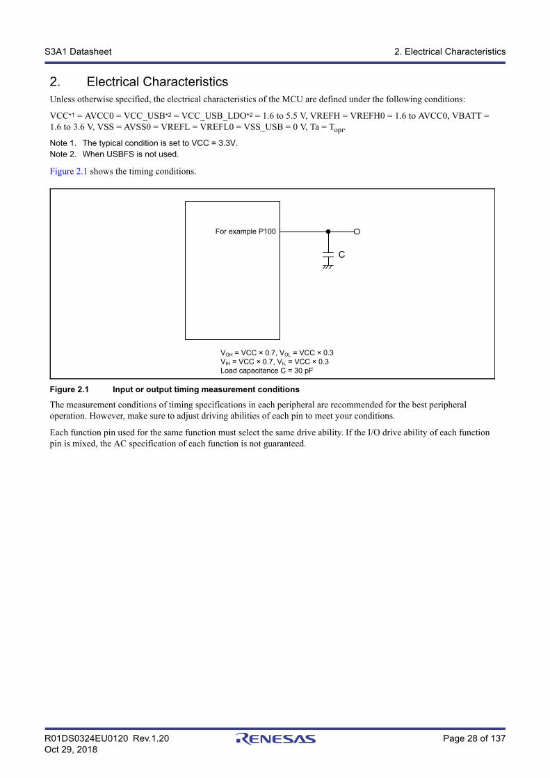
Figure 2.1 shows the timing conditions.
Figure 2.1 Input or output timing measurement conditions
The measurement conditions of timing specifications in each peripheral are recommended for the best peripheral operation. However, make sure to adjust driving abilities of each pin to meet your conditions.
Each function pin used for the same function must select the same drive ability. If the I/O drive ability of each function pin is mixed, the AC specification of each function is not guaranteed.
For example P100
C
VOH = VCC × 0.7, VOL = VCC × 0.3VIH = VCC × 0.7, VIL = VCC × 0.3Load capacitance C = 30 pF
R01DS0324EU0120 Rev.1.20 Page 29 of 137Oct 29, 2018
S3A1 Datasheet 2. Electrical Characteristics
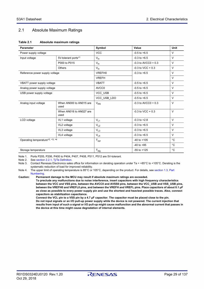
2.1 Absolute Maximum Ratings
Note 1. Ports P205, P206, P400 to P404, P407, P408, P511, P512 are 5V-tolerant.Note 2. See section 2.2.1, Tj/Ta Definition.Note 3. Contact Renesas Electronics sales office for information on derating operation under Ta = +85°C to +105°C. Derating is the
systematic reduction of load for improved reliability.Note 4. The upper limit of operating temperature is 85°C or 105°C, depending on the product. For details, see section 1.3, Part
Numbering.Caution: Permanent damage to the MCU may result if absolute maximum ratings are exceeded.
To preclude any malfunctions due to noise interference, insert capacitors with high frequency characteristics between the VCC and VSS pins, between the AVCC0 and AVSS0 pins, between the VCC_USB and VSS_USB pins, between the VREFH0 and VREFL0 pins, and between the VREFH and VREFL pins. Place capacitors of about 0.1 μF as close as possible to every power supply pin and use the shortest and heaviest possible traces. Also, connect capacitors as stabilization capacitance.Connect the VCL pin to a VSS pin by a 4.7 µF capacitor. The capacitor must be placed close to the pin.Do not input signals or an I/O pull-up power supply while the device is not powered. The current injection that results from input of such a signal or I/O pull-up might cause malfunction and the abnormal current that passes in the device at this time might cause degradation of internal elements.
Table 2.1 Absolute maximum ratings
Parameter Symbol Value Unit
Power supply voltage VCC -0.5 to +6.5 V
Input voltage 5V-tolerant ports*1 Vin -0.3 to +6.5 V
P000 to P015 Vin -0.3 to AVCC0 + 0.3 V
Others Vin -0.3 to VCC + 0.3 V
Reference power supply voltage VREFH0 -0.3 to +6.5 V
VREFH V
VBATT power supply voltage VBATT -0.5 to +6.5 V
Analog power supply voltage AVCC0 -0.5 to +6.5 V
USB power supply voltage VCC_USB -0.5 to +6.5 V
VCC_USB_LDO -0.5 to +6.5 V
Analog input voltage When AN000 to AN015 are used
VAN -0.3 to AVCC0 + 0.3 V
When AN016 to AN027 are used
-0.3 to VCC + 0.3 V
LCD voltage VL1 voltage VL1 -0.3 to +2.8 V
VL2 voltage VL2 -0.3 to +6.5 V
VL3 voltage VL3 -0.3 to +6.5 V
VL4 voltage VL4 -0.3 to +6.5 V
Operating temperature*2, *3, *4 Topr -40 to +105 °C
-40 to +85 °C
Storage temperature Tstg -55 to +125 °C
R01DS0324EU0120 Rev.1.20 Page 30 of 137Oct 29, 2018
S3A1 Datasheet 2. Electrical Characteristics
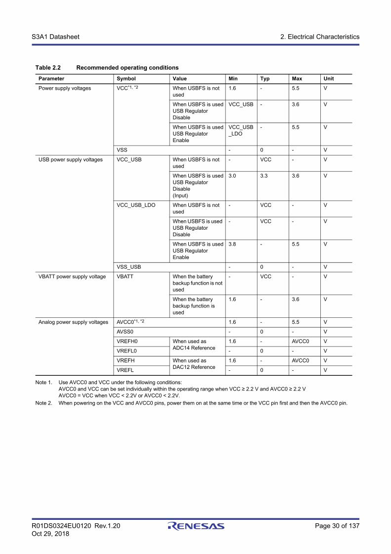
Note 1. Use AVCC0 and VCC under the following conditions:AVCC0 and VCC can be set individually within the operating range when VCC ≥ 2.2 V and AVCC0 ≥ 2.2 VAVCC0 = VCC when VCC < 2.2V or AVCC0 < 2.2V.
Note 2. When powering on the VCC and AVCC0 pins, power them on at the same time or the VCC pin first and then the AVCC0 pin.
Table 2.2 Recommended operating conditions
Parameter Symbol Value Min Typ Max Unit
Power supply voltages VCC*1, *2 When USBFS is not used
1.6 - 5.5 V
When USBFS is usedUSB Regulator Disable
VCC_USB - 3.6 V
When USBFS is usedUSB Regulator Enable
VCC_USB_LDO
- 5.5 V
VSS - 0 - V
USB power supply voltages VCC_USB When USBFS is not used
- VCC - V
When USBFS is usedUSB Regulator Disable(Input)
3.0 3.3 3.6 V
VCC_USB_LDO When USBFS is not used
- VCC - V
When USBFS is used USB Regulator Disable
- VCC - V
When USBFS is usedUSB Regulator Enable
3.8 - 5.5 V
VSS_USB - 0 - V
VBATT power supply voltage VBATT When the battery backup function is not used
- VCC - V
When the battery backup function is used
1.6 - 3.6 V
Analog power supply voltages AVCC0*1, *2 1.6 - 5.5 V
AVSS0 - 0 - V
VREFH0 When used as ADC14 Reference
1.6 - AVCC0 V
VREFL0 - 0 - V
VREFH When used as DAC12 Reference
1.6 - AVCC0 V
VREFL - 0 - V
R01DS0324EU0120 Rev.1.20 Page 31 of 137Oct 29, 2018
S3A1 Datasheet 2. Electrical Characteristics
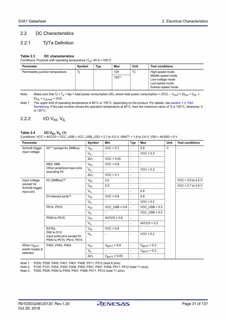
2.2 DC Characteristics
2.2.1 Tj/Ta Definition
Note: Make sure that Tj = Ta + θja × total power consumption (W), where total power consumption = (VCC – VOH) × ΣIOH + VOL ×
ΣIOL + ICCmax × VCC.
Note 1. The upper limit of operating temperature is 85°C or 105°C, depending on the product. For details, see section 1.3, Part Numbering. If the part number shows the operation temperature at 85°C, then the maximum value of Tj is 105°C, otherwise, it is 125°C.
2.2.2 I/O VIH, VIL
Note 1. P205, P206, P400, P401, P407, P408, P511, P512 (total 8 pins).Note 2. P100, P101, P204, P205, P206, P400, P401, P407, P408, P511, P512 (total 11 pins).Note 3. P205, P206, P400 to P404, P407, P408, P511, P512 (total 11 pins).
Table 2.3 DC characteristicsConditions: Products with operating temperature (Ta) -40 to +105°C
Parameter Symbol Typ Max Unit Test conditions
Permissible junction temperature Tj - 125 °C High-speed modeMiddle-speed modeLow-voltage modeLow-speed modeSubosc-speed mode
105*1
Table 2.4 I/O VIH, VIL (1)Conditions: VCC = AVCC0 = VCC_USB = VCC_USB_LDO = 2.7 to 5.5 V, VBATT = 1.6 to 3.6 V, VSS = AVSS0 = 0 V
Parameter Symbol Min Typ Max Unit Test conditions
Schmitt trigger input voltage
IIC*1 (except for SMBus) VIH VCC × 0.7 - 5.8 V -
VIL - - VCC × 0.3
ΔVT VCC × 0.05 - -
RES, NMIOther peripheral input pins excluding IIC
VIH VCC × 0.8 - -
VIL - - VCC × 0.2
ΔVT VCC × 0.1 - -
Input voltage (except for Schmitt trigger input pin)
IIC (SMBus)*2 VIH 2.2 - - VCC = 3.6 to 5.5 V
VIH 2.0 - - VCC = 2.7 to 3.6 V
VIL - - 0.8 -
5V-tolerant ports*3 VIH VCC × 0.8 - 5.8
VIL - - VCC × 0.2
P914, P915 VIH VCC_USB × 0.8 - VCC_USB + 0.3
VIL - - VCC_USB × 0.2
P000 to P015 VIH AVCC0 × 0.8 - -
VIL - - AVCC0 × 0.2
EXTALD00 to D15 Input ports pins except for P000 to P015, P914, P915
VIH VCC × 0.8 - -
VIL - - VCC × 0.2
When VBATT power supply is selected
P402, P403, P404 VIH VBATT × 0.8 - VBATT + 0.3
VIL - - VBATT × 0.2
ΔVT VBATT × 0.05 - -
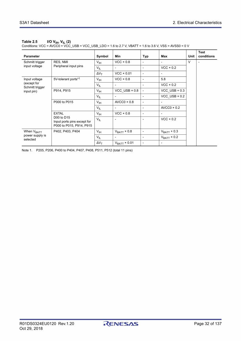
R01DS0324EU0120 Rev.1.20 Page 32 of 137Oct 29, 2018
S3A1 Datasheet 2. Electrical Characteristics
Note 1. P205, P206, P400 to P404, P407, P408, P511, P512 (total 11 pins)
Table 2.5 I/O VIH, VIL (2)Conditions: VCC = AVCC0 = VCC_USB = VCC_USB_LDO = 1.6 to 2.7 V, VBATT = 1.6 to 3.6 V, VSS = AVSS0 = 0 V
Parameter Symbol Min Typ Max UnitTest conditions
Schmitt trigger input voltage
RES, NMIPeripheral input pins
VIH VCC × 0.8 - - V -
VIL - - VCC × 0.2
ΔVT VCC × 0.01 - -
Input voltage (except for Schmitt trigger input pin)
5V-tolerant ports*1 VIH VCC × 0.8 - 5.8
VIL - - VCC × 0.2
P914, P915 VIH VCC_USB × 0.8 - VCC_USB + 0.3
VIL - - VCC_USB × 0.2
P000 to P015 VIH AVCC0 × 0.8 - -
VIL - - AVCC0 × 0.2
EXTALD00 to D15Input ports pins except for P000 to P015, P914, P915
VIH VCC × 0.8 - -
VIL - - VCC × 0.2
When VBATT power supply is selected
P402, P403, P404 VIH VBATT × 0.8 - VBATT + 0.3
VIL - - VBATT × 0.2
ΔVT VBATT × 0.01 - -
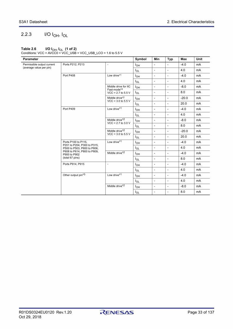
R01DS0324EU0120 Rev.1.20 Page 33 of 137Oct 29, 2018
S3A1 Datasheet 2. Electrical Characteristics
2.2.3 I/O IOH, IOL
Table 2.6 I/O IOH, IOL (1 of 2)Conditions: VCC = AVCC0 = VCC_USB = VCC_USB_LCO = 1.6 to 5.5 V
Parameter Symbol Min Typ Max Unit
Permissible output current (average value per pin)
Ports P212, P213 - IOH - - -4.0 mA
IOL - - 4.0 mA
Port P408 Low drive*1 IOH - - -4.0 mA
IOL - - 4.0 mA
Middle drive for IIC Fast-mode*4
VCC = 2.7 to 5.5 V
IOH - - -8.0 mA
IOL - - 8.0 mA
Middle drive*2
VCC = 3.0 to 5.5 VIOH - - -20.0 mA
IOL - - 20.0 mA
Port P409 Low drive*1 IOH - - -4.0 mA
IOL - - 4.0 mA
Middle drive*2 VCC = 2.7 to 3.0 V
IOH - - -8.0 mA
IOL - - 8.0 mA
Middle drive*2 VCC = 3.0 to 5.5 V
IOH - - -20.0 mA
IOL - - 20.0 mA
Ports P100 to P115, P201 to P204, P300 to P315, P500 to P503, P600 to P606, P608 to P614, P800 to P809, P900 to P902 (total 67 pins)
Low drive*1 IOH - - -4.0 mA
IOL - - 4.0 mA
Middle drive*2 IOH - - -4.0 mA
IOL - - 8.0 mA
Ports P914, P915 - IOH - - -4.0 mA
IOL - - 4.0 mA
Other output pin*3 Low drive*1 IOH - - -4.0 mA
IOL - - 4.0 mA
Middle drive*2 IOH - - -8.0 mA
IOL - - 8.0 mA
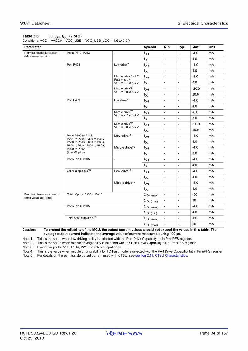
R01DS0324EU0120 Rev.1.20 Page 34 of 137Oct 29, 2018
S3A1 Datasheet 2. Electrical Characteristics
Caution: To protect the reliability of the MCU, the output current values should not exceed the values in this table. The average output current indicates the average value of current measured during 100 μs.
Note 1. This is the value when low driving ability is selected with the Port Drive Capability bit in PmnPFS register.Note 2. This is the value when middle driving ability is selected with the Port Drive Capability bit in PmnPFS register.Note 3. Except for ports P200, P214, P215, which are input ports.Note 4. This is the value when middle driving ability for IIC Fast-mode is selected with the Port Drive Capability bit in PmnPFS register.Note 5. For details on the permissible output current used with CTSU, see section 2.11, CTSU Characteristics.
Permissible output current (Max value per pin)
Ports P212, P213 - IOH - - -4.0 mA
IOL - - 4.0 mA
Port P408 Low drive*1 IOH - - -4.0 mA
IOL - - 4.0 mA
Middle drive for IIC Fast-mode*4
VCC = 2.7 to 5.5 V
IOH - - -8.0 mA
IOL - - 8.0 mA
Middle drive*2
VCC = 3.0 to 5.5 VIOH - - -20.0 mA
IOL - - 20.0 mA
Port P409 Low drive*1 IOH - - -4.0 mA
IOL - - 4.0 mA
Middle drive*2
VCC = 2.7 to 3.0 VIOH - - -8.0 mA
IOL - - 8.0 mA
Middle drive*2 VCC = 3.0 to 5.5 V
IOH - - -20.0 mA
IOL - - 20.0 mA
Ports P100 to P115, P201 to P204, P300 to P315, P500 to P503, P600 to P606, P608 to P614, P800 to P809, P900 to P902(total 67 pins)
Low drive*1 IOH - - -4.0 mA
IOL - - 4.0 mA
Middle drive*2 IOH - - -4.0 mA
IOL - - 8.0 mA
Ports P914, P915 - IOH - - -4.0 mA
IOL - - 4.0 mA
Other output pin*3 Low drive*1 IOH - - -4.0 mA
IOL - - 4.0 mA
Middle drive*2 IOH - - -8.0 mA
IOL - - 8.0 mA
Permissible output current (max value total pins)
Total of ports P000 to P015 ΣIOH (max) - - -30 mA
ΣIOL (max) - - 30 mA
Ports P914, P915 ΣIOH (max) - - -4.0 mA
ΣIOL (min) - - 4.0 mA
Total of all output pin*5 ΣIOH (max) - - -60 mA
ΣIOL (max) - - 60 mA
Table 2.6 I/O IOH, IOL (2 of 2)Conditions: VCC = AVCC0 = VCC_USB = VCC_USB_LCO = 1.6 to 5.5 V
Parameter Symbol Min Typ Max Unit
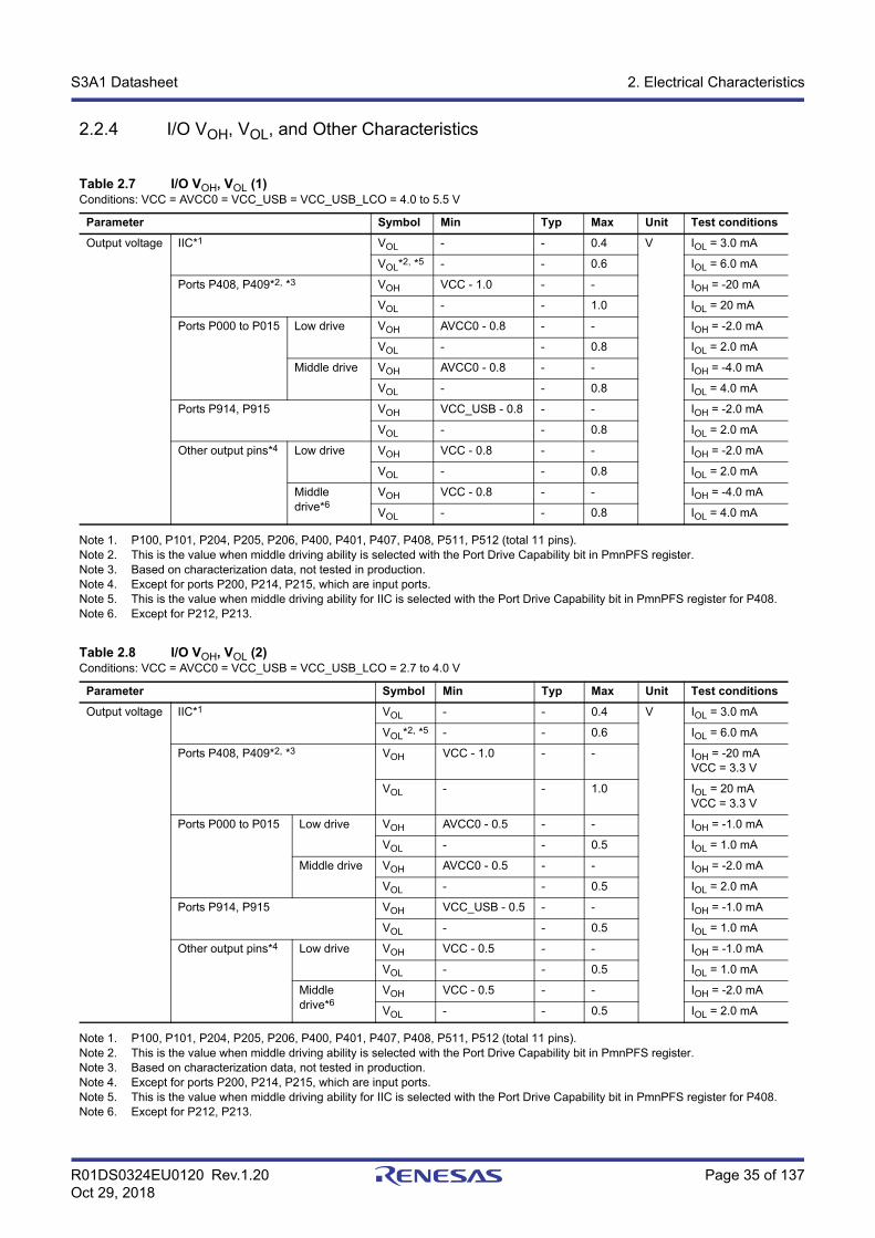
R01DS0324EU0120 Rev.1.20 Page 35 of 137Oct 29, 2018
S3A1 Datasheet 2. Electrical Characteristics
2.2.4 I/O VOH, VOL, and Other Characteristics
Note 1. P100, P101, P204, P205, P206, P400, P401, P407, P408, P511, P512 (total 11 pins).Note 2. This is the value when middle driving ability is selected with the Port Drive Capability bit in PmnPFS register.Note 3. Based on characterization data, not tested in production.Note 4. Except for ports P200, P214, P215, which are input ports.Note 5. This is the value when middle driving ability for IIC is selected with the Port Drive Capability bit in PmnPFS register for P408.Note 6. Except for P212, P213.
Note 1. P100, P101, P204, P205, P206, P400, P401, P407, P408, P511, P512 (total 11 pins).Note 2. This is the value when middle driving ability is selected with the Port Drive Capability bit in PmnPFS register.Note 3. Based on characterization data, not tested in production.Note 4. Except for ports P200, P214, P215, which are input ports.Note 5. This is the value when middle driving ability for IIC is selected with the Port Drive Capability bit in PmnPFS register for P408.Note 6. Except for P212, P213.
Table 2.7 I/O VOH, VOL (1)Conditions: VCC = AVCC0 = VCC_USB = VCC_USB_LCO = 4.0 to 5.5 V
Parameter Symbol Min Typ Max Unit Test conditions
Output voltage IIC*1 VOL - - 0.4 V IOL = 3.0 mA
VOL*2, *5 - - 0.6 IOL = 6.0 mA
Ports P408, P409*2, *3 VOH VCC - 1.0 - - IOH = -20 mA
VOL - - 1.0 IOL = 20 mA
Ports P000 to P015 Low drive VOH AVCC0 - 0.8 - - IOH = -2.0 mA
VOL - - 0.8 IOL = 2.0 mA
Middle drive VOH AVCC0 - 0.8 - - IOH = -4.0 mA
VOL - - 0.8 IOL = 4.0 mA
Ports P914, P915 VOH VCC_USB - 0.8 - - IOH = -2.0 mA
VOL - - 0.8 IOL = 2.0 mA
Other output pins*4 Low drive VOH VCC - 0.8 - - IOH = -2.0 mA
VOL - - 0.8 IOL = 2.0 mA
Middle drive*6
VOH VCC - 0.8 - - IOH = -4.0 mA
VOL - - 0.8 IOL = 4.0 mA
Table 2.8 I/O VOH, VOL (2)Conditions: VCC = AVCC0 = VCC_USB = VCC_USB_LCO = 2.7 to 4.0 V
Parameter Symbol Min Typ Max Unit Test conditions
Output voltage IIC*1 VOL - - 0.4 V IOL = 3.0 mA
VOL*2, *5 - - 0.6 IOL = 6.0 mA
Ports P408, P409*2, *3 VOH VCC - 1.0 - - IOH = -20 mAVCC = 3.3 V
VOL - - 1.0 IOL = 20 mAVCC = 3.3 V
Ports P000 to P015 Low drive VOH AVCC0 - 0.5 - - IOH = -1.0 mA
VOL - - 0.5 IOL = 1.0 mA
Middle drive VOH AVCC0 - 0.5 - - IOH = -2.0 mA
VOL - - 0.5 IOL = 2.0 mA
Ports P914, P915 VOH VCC_USB - 0.5 - - IOH = -1.0 mA
VOL - - 0.5 IOL = 1.0 mA
Other output pins*4 Low drive VOH VCC - 0.5 - - IOH = -1.0 mA
VOL - - 0.5 IOL = 1.0 mA
Middle drive*6
VOH VCC - 0.5 - - IOH = -2.0 mA
VOL - - 0.5 IOL = 2.0 mA
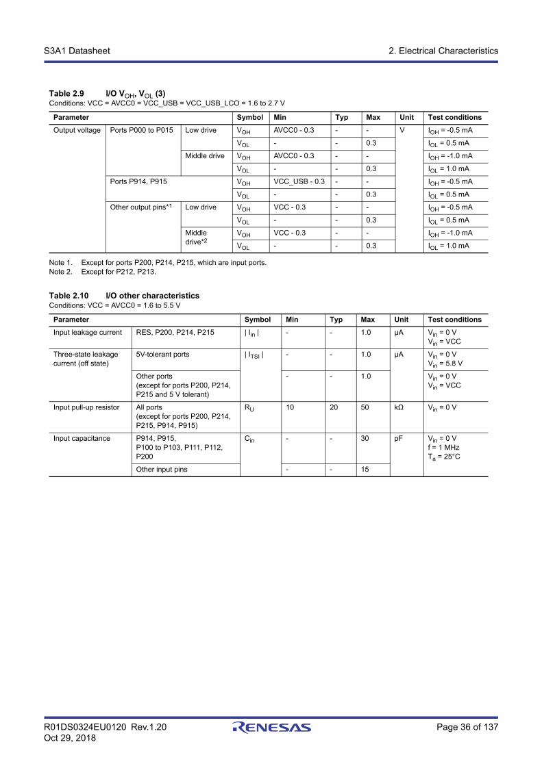
R01DS0324EU0120 Rev.1.20 Page 36 of 137Oct 29, 2018
S3A1 Datasheet 2. Electrical Characteristics
Note 1. Except for ports P200, P214, P215, which are input ports.Note 2. Except for P212, P213.
Table 2.9 I/O VOH, VOL (3)Conditions: VCC = AVCC0 = VCC_USB = VCC_USB_LCO = 1.6 to 2.7 V
Parameter Symbol Min Typ Max Unit Test conditions
Output voltage Ports P000 to P015 Low drive VOH AVCC0 - 0.3 - - V IOH = -0.5 mA
VOL - - 0.3 IOL = 0.5 mA
Middle drive VOH AVCC0 - 0.3 - - IOH = -1.0 mA
VOL - - 0.3 IOL = 1.0 mA
Ports P914, P915 VOH VCC_USB - 0.3 - - IOH = -0.5 mA
VOL - - 0.3 IOL = 0.5 mA
Other output pins*1 Low drive VOH VCC - 0.3 - - IOH = -0.5 mA
VOL - - 0.3 IOL = 0.5 mA
Middle drive*2
VOH VCC - 0.3 - - IOH = -1.0 mA
VOL - - 0.3 IOL = 1.0 mA
Table 2.10 I/O other characteristicsConditions: VCC = AVCC0 = 1.6 to 5.5 V
Parameter Symbol Min Typ Max Unit Test conditions
Input leakage current RES, P200, P214, P215 | Iin | - - 1.0 μA Vin = 0 VVin = VCC
Three-state leakage current (off state)
5V-tolerant ports | ITSI | - - 1.0 μA Vin = 0 VVin = 5.8 V
Other ports (except for ports P200, P214, P215 and 5 V tolerant)
- - 1.0 Vin = 0 VVin = VCC
Input pull-up resistor All ports (except for ports P200, P214, P215, P914, P915)
RU 10 20 50 kΩ Vin = 0 V
Input capacitance P914, P915, P100 to P103, P111, P112, P200
Cin - - 30 pF Vin = 0 Vf = 1 MHzTa = 25°C
Other input pins - - 15
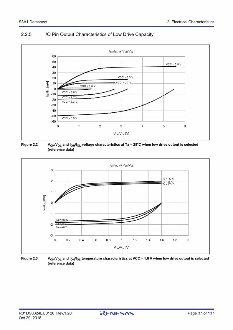
R01DS0324EU0120 Rev.1.20 Page 37 of 137Oct 29, 2018
S3A1 Datasheet 2. Electrical Characteristics
2.2.5 I/O Pin Output Characteristics of Low Drive Capacity
Figure 2.2 VOH/VOL and IOH/IOL voltage characteristics at Ta = 25°C when low drive output is selected
(reference data)
Figure 2.3 VOH/VOL and IOH/IOL temperature characteristics at VCC = 1.6 V when low drive output is selected
(reference data)
0 1 2 3 4 5 6
-60
-50
-40
-30
-20
-10
0
10
20
30
40
50
60
IOH/IOL vs VOH/VOL
VOH/VOL [V]
I OH/I O
L[m
A]
VCC = 5.5 V
VCC = 3.3 V
VCC = 2.7 V
VCC = 1.6 V
VCC = 1.6 VVCC = 2.7 V
VCC = 3.3 V
VCC = 5.5 V
0 0.2 0.4 0.6 0.8 1 1.2 1.4 1.6 1.8 2
-3
-2
-1
0
1
2
3
IOH/IOL vs VOH/VOL
VOH/VOL [V]
I OH/I O
L[m
A]
Ta = -40°C
Ta = 105 °C
Ta = 25°C
Ta = 105°C
Ta = -40°CTa = 25°C
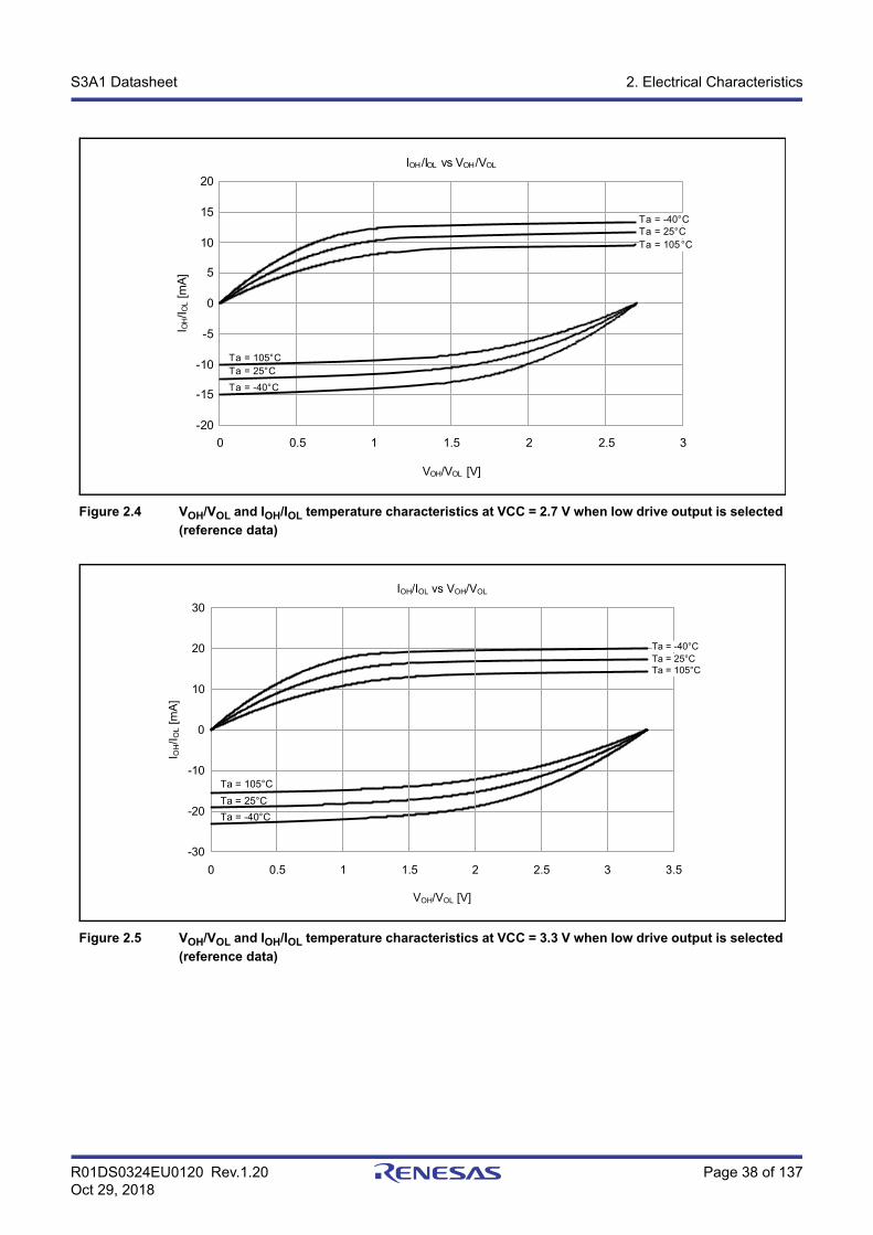
R01DS0324EU0120 Rev.1.20 Page 38 of 137Oct 29, 2018
S3A1 Datasheet 2. Electrical Characteristics
Figure 2.4 VOH/VOL and IOH/IOL temperature characteristics at VCC = 2.7 V when low drive output is selected
(reference data)
Figure 2.5 VOH/VOL and IOH/IOL temperature characteristics at VCC = 3.3 V when low drive output is selected
(reference data)
0 0.5 1 1.5 2 2.5 3
-20
-15
-10
-5
0
5
10
15
20
IOH/IOL vs VOH/VOL
VOH/VOL [V]
I OH/I O
L[m
A]
Ta = -40°C
Ta = 105°CTa = 25°C
Ta = 105°C
Ta = -40°CTa = 25°C
0 0.5 1 1.5 2 2.5 3 3.5
-30
-20
-10
0
10
20
30
IOH/IOL vs VOH/VOL
VOH/VOL [V]
I OH/I
OL
[mA
]
Ta = -40°C
Ta = 105°C
Ta = 25°C
Ta = 105°C
Ta = -40°CTa = 25°C
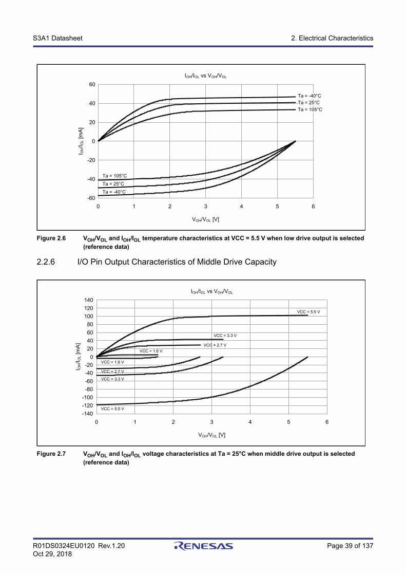
R01DS0324EU0120 Rev.1.20 Page 39 of 137Oct 29, 2018
S3A1 Datasheet 2. Electrical Characteristics
Figure 2.6 VOH/VOL and IOH/IOL temperature characteristics at VCC = 5.5 V when low drive output is selected
(reference data)
2.2.6 I/O Pin Output Characteristics of Middle Drive Capacity
Figure 2.7 VOH/VOL and IOH/IOL voltage characteristics at Ta = 25°C when middle drive output is selected
(reference data)
0 1 2 3 4 5 6
-60
-40
-20
0
20
40
60
IOH/IOL vs VOH/VOL
VOH/VOL [V]
I OH/I
OL
[mA
]
Ta = -40°C
Ta = 105°C
Ta = 25°C
Ta = 105°C
Ta = -40°C
Ta = 25°C
0 1 2 3 4 5 6
-140
-120
-100
-80
-60
-40
-20
0
20
40
60
80
100
120
140
IOH/IOL vs VOH/VOL
VOH/VOL [V]
I OH/I O
L [m
A]
VCC = 5.5 V
VCC = 3.3 V
VCC = 2.7 V
VCC = 1.6 V
VCC = 1.6 V
VCC = 2.7 V
VCC = 3.3 V
VCC = 5.5 V
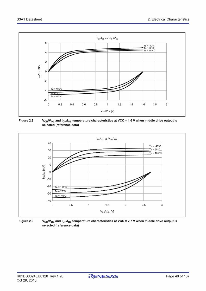
R01DS0324EU0120 Rev.1.20 Page 40 of 137Oct 29, 2018
S3A1 Datasheet 2. Electrical Characteristics
Figure 2.8 VOH/VOL and IOH/IOL temperature characteristics at VCC = 1.6 V when middle drive output is
selected (reference data)
Figure 2.9 VOH/VOL and IOH/IOL temperature characteristics at VCC = 2.7 V when middle drive output is
selected (reference data)
0 0.2 0.4 0.6 0.8 1 1.2 1.4 1.6 1.8 2
-6
-4
-2
0
2
4
6
IOH/IOL vs VOH/VOL
VOH/VOL [V]
I OH/I
OL
[mA
]
Ta = -40°C
Ta = 105°C
Ta = 25°C
Ta = 105°C
Ta = -40°CTa = 25°C
0 0.5 1 1.5 2 2.5 3
-40
-30
-20
-10
0
10
20
30
40
IOH/IOL vs VOH/VOL
VOH/VOL [V]
I OH/I
OL [m
A]
Ta = -40°C
Ta = 105°C
Ta = 25°C
Ta = 105°C
Ta = -40°CTa = 25°C
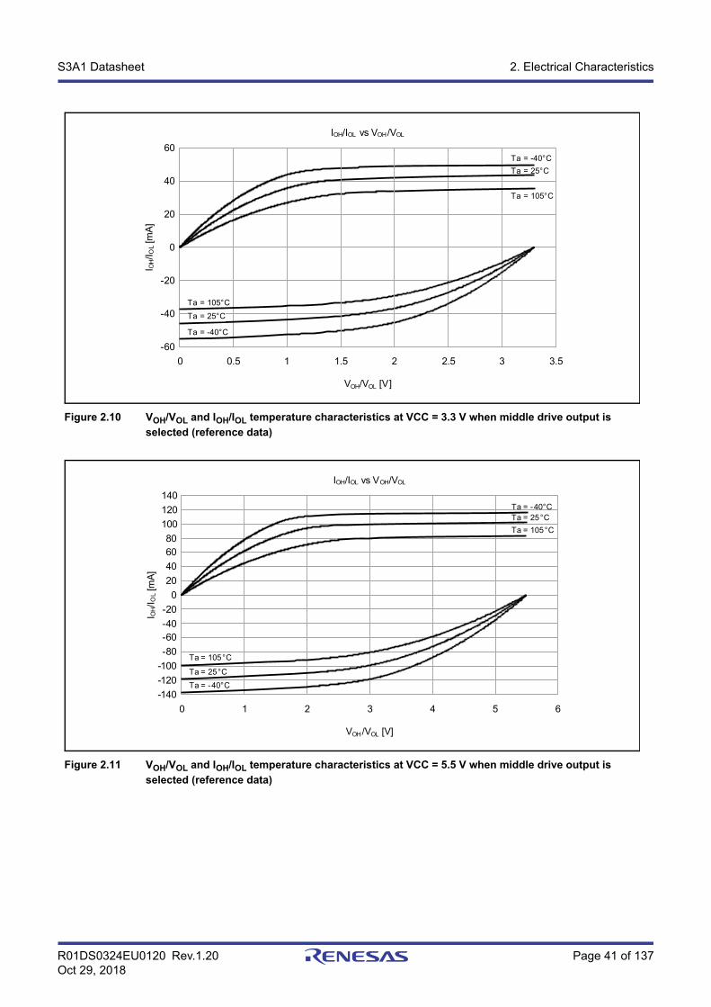
R01DS0324EU0120 Rev.1.20 Page 41 of 137Oct 29, 2018
S3A1 Datasheet 2. Electrical Characteristics
Figure 2.10 VOH/VOL and IOH/IOL temperature characteristics at VCC = 3.3 V when middle drive output is
selected (reference data)
Figure 2.11 VOH/VOL and IOH/IOL temperature characteristics at VCC = 5.5 V when middle drive output is
selected (reference data)
0 0.5 1 1.5 2 2.5 3 3.5
-60
-40
-20
0
20
40
60
IOH/IOL vs VOH/VOL
VOH/VOL [V]
I OH/I O
L[m
A]
Ta = -40°C
Ta = 105°C
Ta = 25°C
Ta = 105°C
Ta = -40°C
Ta = 25°C
0 1 2 3 4 5 6
-140
-120
-100
-80
-60 -40
-20
0
20
40
60 80
100
120
140
IOH/IOL vs VOH/VOL
VOH/VOL [V]
I OH/I O
L[m
A]
Ta = -40°C
Ta = 105°C
Ta = 25°C
Ta = 105°C
Ta = -40°CTa = 25°C
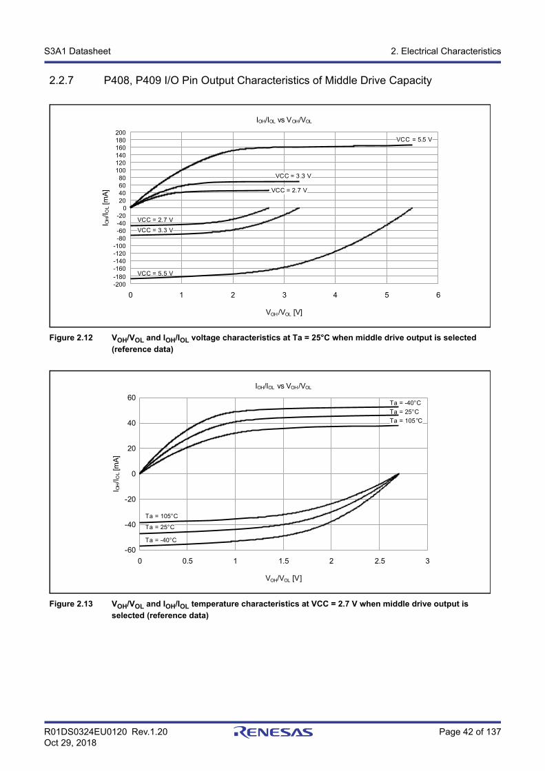
R01DS0324EU0120 Rev.1.20 Page 42 of 137Oct 29, 2018
S3A1 Datasheet 2. Electrical Characteristics
2.2.7 P408, P409 I/O Pin Output Characteristics of Middle Drive Capacity
Figure 2.12 VOH/VOL and IOH/IOL voltage characteristics at Ta = 25°C when middle drive output is selected
(reference data)
Figure 2.13 VOH/VOL and IOH/IOL temperature characteristics at VCC = 2.7 V when middle drive output is
selected (reference data)
0 1 2 3 4 5 6
IOH/IOL vs VOH/VOL
VOH/VOL [V]
I OH/I O
L[m
A]
VCC = 5.5 V
VCC = 3.3 V
VCC = 2.7 V
VCC = 2.7 V
VCC = 3.3 V
VCC = 5.5 V
-140 -120 -100
-80 -60 -40 -20
20 40 60 80
100 120 140
200180160
0
-160 -180 -200
0 0.5 1 1.5 2 2.5 3
-60
-40
-20
0
20
40
60
IOH/IOL vs VOH/VOL
VOH/VOL [V]
I OH/I O
L[m
A]
Ta = -40°C
Ta = 105°C
Ta = 25°C
Ta = 105°C
Ta = -40°C
Ta = 25°C
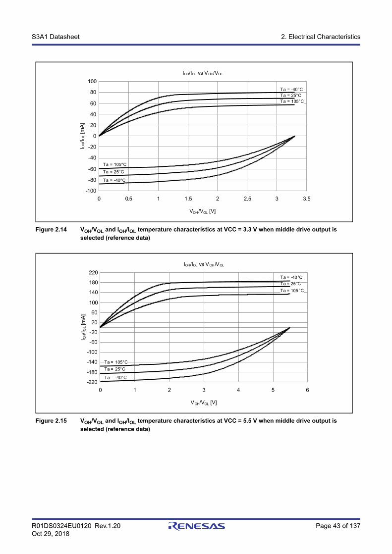
R01DS0324EU0120 Rev.1.20 Page 43 of 137Oct 29, 2018
S3A1 Datasheet 2. Electrical Characteristics
Figure 2.14 VOH/VOL and IOH/IOL temperature characteristics at VCC = 3.3 V when middle drive output is
selected (reference data)
Figure 2.15 VOH/VOL and IOH/IOL temperature characteristics at VCC = 5.5 V when middle drive output is
selected (reference data)
0 0.5 1 1.5 2 2.5 3 3.5
-100
-80
-60
-40
-20
0
20
40
60
80
100
IOH/IOL vs VOH/VOL
VOH/VOL [V]
I OH/I O
L[m
A]
Ta = -40°C
Ta = 105°C
Ta = 25°C
Ta = 105°C
Ta = -40°CTa = 25°C
0 1 2 3 4 5 6
-220
-180
-140
-100
-60
-20
20
60
100
140
180
220
IOH/IOL vs VOH/VOL
VOH/VOL [V]
I OH/I O
L[m
A]
Ta = -40°C
Ta = 105°C
Ta = 25°C
Ta = 105°C
Ta = -40°C
Ta = 25°C
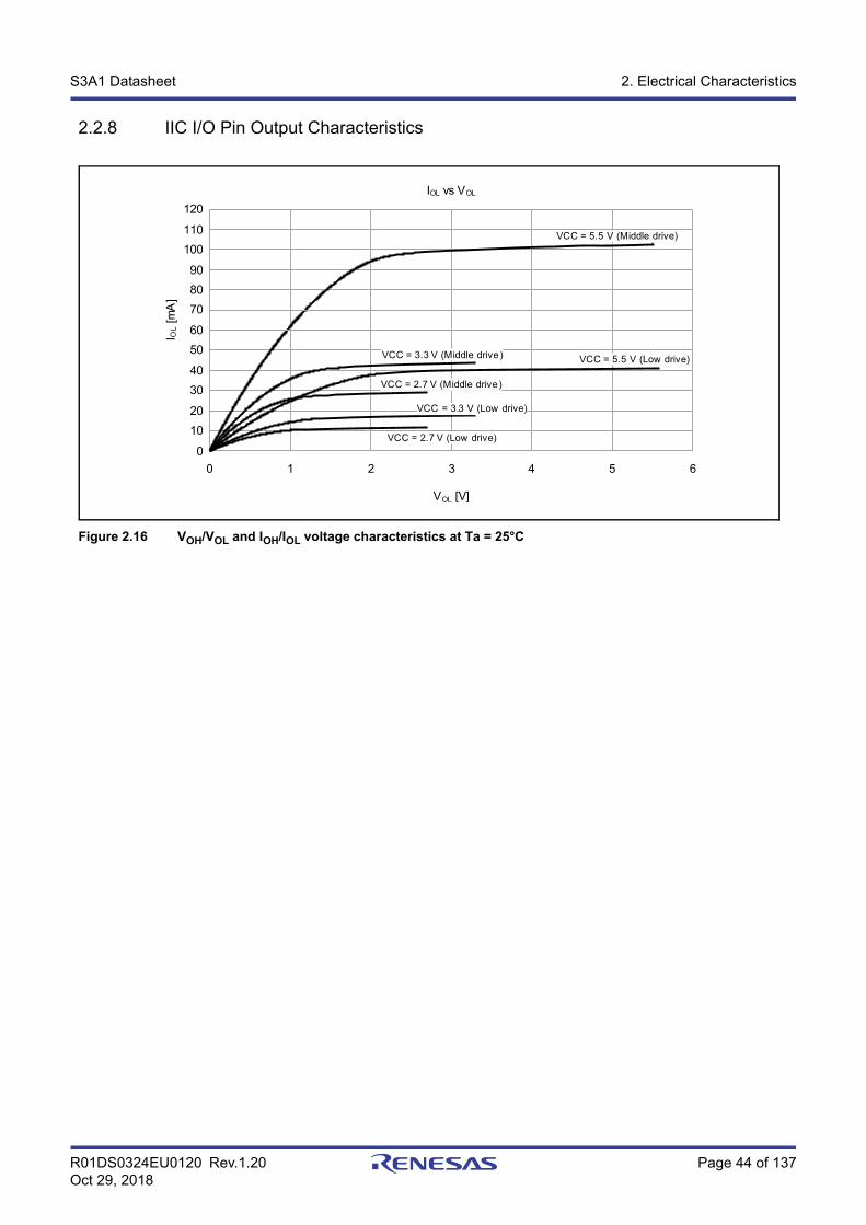
R01DS0324EU0120 Rev.1.20 Page 44 of 137Oct 29, 2018
S3A1 Datasheet 2. Electrical Characteristics
2.2.8 IIC I/O Pin Output Characteristics
Figure 2.16 VOH/VOL and IOH/IOL voltage characteristics at Ta = 25°C
0 1 2 3 4 5 6
0
10
20
30
40
50
60
70
80
90
100
110
120
IOL vs VOL
VOL [V]
I OL
[mA
]
VCC = 2.7 V (Low drive)
VCC = 3.3 V (Low drive)
VCC = 5.5 V (Low drive)
VCC = 5.5 V (Middle drive)
VCC = 3.3 V (Middle drive)
VCC = 2.7 V (Middle drive)
R01DS0324EU0120 Rev.1.20 Page 45 of 137Oct 29, 2018
S3A1 Datasheet 2. Electrical Characteristics
2.2.9 Operating and Standby Current
Table 2.11 Operating and standby current (1) (1 of 2)Conditions: VCC = AVCC0 = 1.6 to 5.5 V
Parameter Symbol Typ*10 Max UnitTest conditions
Supply current*1
High-speed mode*2
Normal mode All peripheral clocks disabled, while (1) code executing from flash*5
ICLK = 48 MHz ICC 9.3 - mA *7
ICLK = 32 MHz 6.7 -
ICLK = 16 MHz 4.1 -
ICLK = 8 MHz 2.7 -
All peripheral clocks disabled, CoreMark code executing from flash*5
ICLK = 48 MHz 18.8 -
ICLK = 32 MHz 13.1 -
ICLK = 16 MHz 7.5 -
ICLK = 8 MHz 4.7 -
All peripheral clocks enabled, while (1) code executing from flash*5
ICLK = 48 MHz 22.4 - *9
ICLK = 32 MHz 16.9 - *8
ICLK = 16 MHz 9.4 -
ICLK = 8 MHz 5.5 -
All peripheral clocks enabled, code executing from SRAM*5
ICLK = 48 MHz - 62.0 *9
Sleep mode All peripheral clocks disabled*5
ICLK = 48 MHz 4.0 - *7
ICLK = 32 MHz 3.1 -
ICLK = 16 MHz 2.3 -
ICLK = 8 MHz 1.8 -
All peripheral clocks enabled*5
ICLK = 48 MHz 16.8 - *9
ICLK = 32 MHz 13.0 - *8
ICLK = 16 MHz 7.4 -
ICLK = 8 MHz 4.5 -
Increase during BGO operation*6 2.5 - -
Middle-speed mode*2
Normal mode All peripheral clocks disabled, while (1) code executing from flash*5
ICLK = 12 MHz ICC 2.8 - mA *7
ICLK = 8 MHz 2.3 -
ICLK = 1 MHz 1.1 -
All peripheral clocks disabled, CoreMark code executing from flash*5
ICLK = 12 MHz 5.4 -
ICLK = 8 MHz 4.2 -
ICLK = 1 MHz 1.4 -
All peripheral clocks enabled, while (1) code executing from flash*5
ICLK = 12 MHz 6.9 - *8
ICLK = 8 MHz 5.1 -
ICLK = 1 MHz 1.7 -
All peripheral clocks enabled, code executing from SRAM*5
ICLK = 12 MHz - 25.0
Sleep mode All peripheral clocks disabled*5
ICLK = 12 MHz 1.5 - *7
ICLK = 8 MHz 1.4 -
ICLK = 1 MHz 1.0 -
All peripheral clocks enabled*5
ICLK = 12 MHz 5.4 - *8
ICLK = 8 MHz 4.1 -
ICLK = 1 MHz 1.6 -
Increase during BGO operation*6 2.5 - -
R01DS0324EU0120 Rev.1.20 Page 46 of 137Oct 29, 2018
S3A1 Datasheet 2. Electrical Characteristics
Note 1. Supply current values do not include output charge/discharge current from all pins. The values apply when internal pull-up MOSs are in the off state.
Note 2. The clock source is HOCO.Note 3. The clock source is MOCO.Note 4. The clock source is the sub-clock oscillator.Note 5. This does not include BGO operation.Note 6. This is the increase for programming or erasure of the flash memory for data storage during program execution.Note 7. FCLK, BCLK, PCLKA, PCLKB, PCLKC, and PCLKD are set to divided by 64.Note 8. FCLK, BCLK, PCLKA, PCLKB, PCLKC, and PCLKD are the same frequency as that of ICLK.Note 9. FCLK, BCLK, and PCLKB are set to divided by 2 and PCLKA, PCLKC, and PCLKD are the same frequency as that of ICLK.Note 10. VCC = 3.3 V.
Supply current*1
Low-speed mode*3
Normal mode All peripheral clocks
disabled, while (1) code
executing from flash*5
ICLK = 1 MHz ICC 0.4 - mA *7
All peripheral clocks disabled, CoreMark code executing from flash*5
ICLK = 1 MHz 0.6 -
All peripheral clocks enabled, while (1) code executing from flash*5
ICLK = 1 MHz 1.1 - *8
All peripheral clocks enabled, code executing from SRAM*5
ICLK = 1 MHz - 2.6
Sleep mode All peripheral clocks disabled*5
ICLK = 1 MHz 0.3 - *7
All peripheral clocks enabled*5
ICLK = 1 MHz 1.0 - *8
Low-voltage mode*3
Normal mode All peripheral clocks disabled, while (1) code executing from flash*5
ICLK = 4 MHz ICC 2.2 - mA *7
All peripheral clocks disabled, CoreMark code executing from flash*5
ICLK = 4 MHz 3.3 -
All peripheral clocks enabled, while (1) code executing from flash*5
ICLK = 4 MHz 3.7 - *8
All peripheral clocks enabled, code executing from SRAM*5
ICLK = 4 MHz - 10.0
Sleep mode All peripheral clocks disabled*5
ICLK = 4 MHz 1.7 - *7
All peripheral clocks enabled*5
ICLK = 4 MHz 3.2 - *8
Subosc-speed mode*4
Normal mode All peripheral clocks disabled, while (1) code executing from flash*5
ICLK = 32.768 kHz ICC 10.0 - μA *8
All peripheral clocks enabled, while (1) code executing from flash*5
ICLK = 32.768 kHz 17.9 -
All peripheral clocks enabled, code executing from SRAM*5
ICLK = 32.768 kHz - 154.0
Sleep mode All peripheral clocks disabled*5
ICLK = 32.768 kHz 6.3 -
All peripheral clocks enabled*5
ICLK = 32.768 kHz 14.0 -
Table 2.11 Operating and standby current (1) (2 of 2)Conditions: VCC = AVCC0 = 1.6 to 5.5 V
Parameter Symbol Typ*10 Max UnitTest conditions
R01DS0324EU0120 Rev.1.20 Page 47 of 137Oct 29, 2018
S3A1 Datasheet 2. Electrical Characteristics
Figure 2.17 Voltage dependency in high-speed mode (reference data)
Figure 2.18 Voltage dependency in middle-speed mode (reference data)
0
10
20
30
40
50
1.5 2.0 2.5 3.0 3.5 4.0 4.5 5.0 5.5 6.0
ICC
(mA)
VCC(V)Ta = 25 , ICLK = 48 MHz *Ta = 25 , ICLK = 32 MHz *Ta = 25 , ICLK = 16 MHz *1
Ta = 25 , ICLK = 8 MHz *1
Ta = 25 , ICLK = 4 MHz *1
Ta = 105 , ICLK = 48 MHz *2
Ta = 105 , ICLK = 32 MHz *2
Ta = 105 , ICLK = 16 MHz *2
Ta = 105 , ICLK = 8 MHz *2
Ta = 105 , ICLK = 4 MHz *2
Note 1. All peripheral operations except any BGO operation are operating normally. This is the average of the actu measurements of the sample cores during product evaluation.Note 2. All peripheral operations except any BGO operation are operating at maximum. This is the average of the
Ta = 105 , ICLK = 48 MHz*2
Ta = 25 , ICLK = 48 MHz*1
Ta = 105 , ICLK = 32 MHz*2
Ta = 105 , ICLK = 16 MHz*2
Ta = 105 , ICLK = 8 MHz*2
Ta = 105 , ICLK = 4 MHz*2
Ta = 25 , ICLK = 32 MHz*1
Ta = 25 , ICLK = 16 MHz*1
Ta = 25 , ICLK = 8 MHz*1Ta = 25 , ICLK = 4 MHz*1
0
5
10
15
1.5 2.0 2.5 3.0 3.5 4.0 4.5 5.0 5.5 6.0
ICC
(mA)
VCC (V)Ta = 25 , ICLK = 12 MHz *1 Ta = 105 , ICLK = 12 MHz *2
Ta = 25 , ICLK = 8 MHz *1
Ta = 25 , ICLK = 4 MHz *1
Ta = 25 , ICLK = 1 MHz *1
Ta = 105 , ICLK = 8 MHz *2
Ta = 105 , ICLK = 4 MHz *2
Ta = 105 , ICLK = 1 MHz *2
Note 1. All peripheral operations except any BGO operation are operating normally. This is the average of the actuameasurements of the sample cores during product evaluation.Note 2. All peripheral operations except any BGO operation are operating at maximum. This is the average of theactual measurements for the upper-limit samples during product evaluation.
Ta = 105 , ICLK = 12 MHz*2
Ta = 105 , ICLK = 8 MHz*2
Ta = 25 , ICLK = 4 MHz*1Ta = 105 , ICLK = 1 MHz*2Ta = 25 , ICLK = 1 MHz*1
Ta = 25 , ICLK = 12 MHz*1
Ta = 105 , ICLK = 4 MHz*2
Ta = 25 , ICLK = 8 MHz*1
R01DS0324EU0120 Rev.1.20 Page 48 of 137Oct 29, 2018
S3A1 Datasheet 2. Electrical Characteristics
Figure 2.19 Voltage dependency in low-speed mode (reference data)
Figure 2.20 Voltage dependency in low-voltage mode (reference data)
0.00.20.40.60.81.01.21.41.61.82.0
1.5 2.0 2.5 3.0 3.5 4.0 4.5 5.0 5.5 6.0
ICC(A)
VCC(V)Ta = 25 , ICLK = 1 MHz *1 Ta = 105 , ICLK = 1 MHz *2
Note 1. All peripheral operations except any BGO operation are operating normally. This is the average of the actuameasurements of the sample cores during product evaluation.Note 2. All peripheral operations except any BGO operation are operating at maximum. This is the average of theactual measurements for the upper-limit samples during product evaluation.
Ta = 105 , ICLK = 1 MHz*2
Ta = 25 , ICLK = 1 MHz*1
0
1
2
3
4
5
6
7
1.5 2.0 2.5 3.0 3.5 4.0 4.5 5.0 5.5 6.0
ICC
(mA)
VCC (V)Ta = 25 , ICLK = 4 MHz *1
Ta = 25 , ICLK = 1 MHz *1Ta = 105 , ICLK = 4 MHz *2
Ta = 105 , ICLK = 1 MHz *2
Note 1. All peripheral operations except any BGO operation are operating normally. This is the average of theactu measurements of the sample cores during product evaluation.Note 2. All peripheral operations except any BGO operation are operating at maximum. This is the average of theactual measurements for the upper-limit samples during product evaluation.
Ta = 105 , ICLK = 4 MHz*2
Ta = 25 , ICLK = 4 MHz*1
Ta = 105 , ICLK = 1 MHz*2
Ta = 25 , ICLK = 1 MHz*1
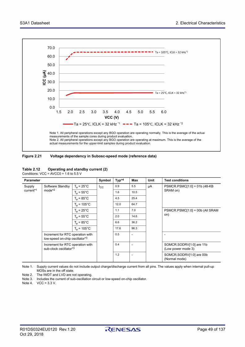
R01DS0324EU0120 Rev.1.20 Page 49 of 137Oct 29, 2018
S3A1 Datasheet 2. Electrical Characteristics
Figure 2.21 Voltage dependency in Subosc-speed mode (reference data)
Note 1. Supply current values do not include output charge/discharge current from all pins. The values apply when internal pull-up MOSs are in the off state.
Note 2. The IWDT and LVD are not operating.Note 3. Includes the current of sub-oscillation circuit or low-speed on-chip oscillator.Note 4. VCC = 3.3 V.
Table 2.12 Operating and standby current (2)Conditions: VCC = AVCC0 = 1.6 to 5.5 V
Parameter Symbol Typ*4 Max Unit Test conditions
Supply current*1
Software Standby mode*2
Ta = 25°C ICC 0.9 5.5 μA PSMCR.PSMC[1:0] = 01b (48-KB SRAM on)
Ta = 55°C 1.6 10.5
Ta = 85°C 4.5 25.4
Ta = 105°C 12.0 64.7
Ta = 25°C 1.1 7.0 PSMCR.PSMC[1:0] = 00b (All SRAM on)
Ta = 55°C 2.0 14.6
Ta = 85°C 6.6 36.2
Ta = 105°C 17.6 96.3
Increment for RTC operation with low-speed on-chip oscillator*3
0.5 - -
Increment for RTC operation with sub-clock oscillator*3
0.4 - SOMCR.SODRV[1:0] are 11b (Low power mode 3)
1.2 - SOMCR.SODRV[1:0] are 00b (Normal mode)
0.0
10.0
20.0
30.0
40.0
50.0
60.0
70.0
1.5 2.0 2.5 3.0 3.5 4.0 4.5 5.0 5.5 6.0
ICC
(A
)
VCC (V)Ta = 25 , ICLK = 32 kHz *1 Ta = 105 , ICLK = 32 kHz *2
Note 1. All peripheral operations except any BGO operation are operating normally. This is the average of the actualmeasurements of the sample cores during product evaluation.Note 2. All peripheral operations except any BGO operation are operating at maximum. This is the average of theactual measurements for the upper-limit samples during product evaluation.
Ta = 105 , ICLK = 32 kHz*2
Ta = 25 , ICLK = 32 kHz*1
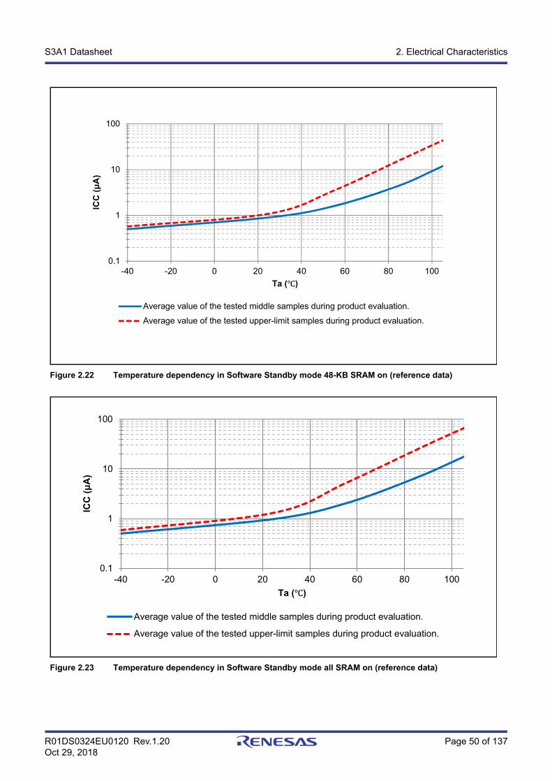
R01DS0324EU0120 Rev.1.20 Page 50 of 137Oct 29, 2018
S3A1 Datasheet 2. Electrical Characteristics
Figure 2.22 Temperature dependency in Software Standby mode 48-KB SRAM on (reference data)
Figure 2.23 Temperature dependency in Software Standby mode all SRAM on (reference data)
0.1
1
10
100
-40 -20 0 20 40 60 80 100
ICC
(A
)
Ta ( )
Average value of the tested middle samples during product evaluation.Average value of the tested upper-limit samples during product evaluation.
0.1
1
10
100
-40 -20 0 20 40 60 80 100
ICC
(A
)
Ta ( )
Average value of the tested middle samples during product evaluation.
Average value of the tested upper-limit samples during product evaluation.
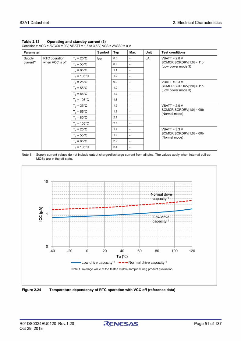
R01DS0324EU0120 Rev.1.20 Page 51 of 137Oct 29, 2018
S3A1 Datasheet 2. Electrical Characteristics
Note 1. Supply current values do not include output charge/discharge current from all pins. The values apply when internal pull-up MOSs are in the off state.
Figure 2.24 Temperature dependency of RTC operation with VCC off (reference data)
Table 2.13 Operating and standby current (3)Conditions: VCC = AVCC0 = 0 V, VBATT = 1.6 to 3.6 V, VSS = AVSS0 = 0 V
Parameter Symbol Typ Max Unit Test conditions
Supply current*1
RTC operation when VCC is off
Ta = 25°C ICC 0.8 - μA VBATT = 2.0 VSOMCR.SORDRV[1:0] = 11b(Low power mode 3)
Ta = 55°C 0.9 -
Ta = 85°C 1.1 -
Ta = 105°C 1.2 -
Ta = 25°C 0.9 - VBATT = 3.3 VSOMCR.SORDRV[1:0] = 11b(Low power mode 3)
Ta = 55°C 1.0 -
Ta = 85°C 1.2 -
Ta = 105°C 1.3 -
Ta = 25°C 1.6 - VBATT = 2.0 VSOMCR.SORDRV[1:0] = 00b(Normal mode)
Ta = 55°C 1.8 -
Ta = 85°C 2.1 -
Ta = 105°C 2.3 -
Ta = 25°C 1.7 - VBATT = 3.3 VSOMCR.SORDRV[1:0] = 00b(Normal mode)
Ta = 55°C 1.9 -
Ta = 85°C 2.2 -
Ta = 105°C 2.4 -
Note 1. Average value of the tested middle sample during product evaluation.
Low drive capacity*1
Normal drive capacity*1
0
1
10
-40 -20 0 20 40 60 80 100 120
ICC
(A
)
Ta ( )Low drive capacity*1 Normal drive capacity*1
R01DS0324EU0120 Rev.1.20 Page 52 of 137Oct 29, 2018
S3A1 Datasheet 2. Electrical Characteristics
Note 1. The reference power supply current is included in the power supply current value for D/A conversion.Note 2. Current consumed only by the USBFS.Note 3. Includes the current supplied from the pull-up resistor of the USB_DP pin to the pull-down resistor of the host device, in addition
to the current consumed by the MCU during the suspended state.Note 4. When VCC = VCC_USB = 3.3 V.Note 5. Current flowing only to the LCD controller. Not including the current that flows through the LCD panel.Note 6. When the MCU is in Software Standby mode or the MSTPCRD.MSTPD16 (ADC140 Module Stop bit) is in the module-stop
state.
Table 2.14 Operating and standby current (4)Conditions: VCC = AVCC0 = 1.6 to 5.5 V, VREFH0 = 2.7 V to AVCC0
Parameter Symbol Min Typ Max UnitTest conditions
Analog power supply current
During A/D conversion (at high-speed conversion) IAVCC - - 3.0 mA -
During A/D conversion (at low power conversion) - - 1.0 mA -
During D/A conversion (per channel)*1 - 0.4 0.8 mA -
Waiting for A/D and D/A conversion (all units)*6 - - 1.0 μA -
Reference power supply current
During A/D conversion IREFH0 - - 150 μA -
Waiting for A/D conversion (all units) - - 60 nA -
During D/A conversion IREFH - 50 100 μA -
Waiting for D/A conversion (all units) - - 100 μA -
Temperature sensor ITNS - 75 - μA -
Low-Power Analog Comparator operating current
Window mode ICMPLP - 15 - μA -
Comparator High-speed mode - 10 - μA -
Comparator Low-speed mode - 2 - μA -
Comparator Low-speed mode using DAC8 - 820 - μA -
Operational Amplifier operating current
Low power mode 1 unit operating IAMP - 2.5 4.0 μA -
2 units operating - 4.5 8.0 μA -
3 units operating - 6.5 11.0 μA -
4 units operating - 8.5 14.0 μA -
High speed mode 1 unit operating - 140 220 μA -
2 units operating - 280 410 μA -
3 units operating - 420 600 μA -
4 units operating - 560 780 μA -
LCD operating current
External resistance division methodfLCD = fSUB = 128 Hz, 1/3 bias, and 4-time slice
ILCD1*5 - 0.34 - μA -
Internal voltage boosting method (VLCD.VLCD = 04)fLCD = fSUB = 128 Hz, 1/3 bias, and 4-time slice
ILCD2*5 - 0.92 - μA -
Capacitor split methodfLCD = fSUB = 128 Hz, 1/3 bias, and 4-time slice
ILCD3*5 - 0.19 - μA -
USB operating current
During USB communication operation under the following settings and conditions: Host controller operation is set to full-speed mode
Bulk OUT transfer (64 bytes) × 1,bulk IN transfer (64 bytes) × 1
Connect peripheral devices via a 1-meter USB cable from the USB port.
IUSBH*2 - 4.3 (VCC)0.9 (VCC_USB)*4
- mA -
During USB communication operation under the following settings and conditions: Device controller operation is set to full-speed mode
Bulk OUT transfer (64 bytes) × 1,bulk IN transfer (64 bytes) × 1
Connect the host device via a 1-meter USB cable from the USB port.
IUSBF*2 - 3.6 (VCC)1.1 (VCC_USB)*4
- mA -
During suspended state under the following setting and conditions: Device controller operation is set to full-speed mode
(pull up the USB_DP pin) Software standby mode Connect the host device via a 1-meter USB cable
from the USB port.
ISUSP*3 - 0.35 (VCC)170 (VCC_USB)*4
- μA -
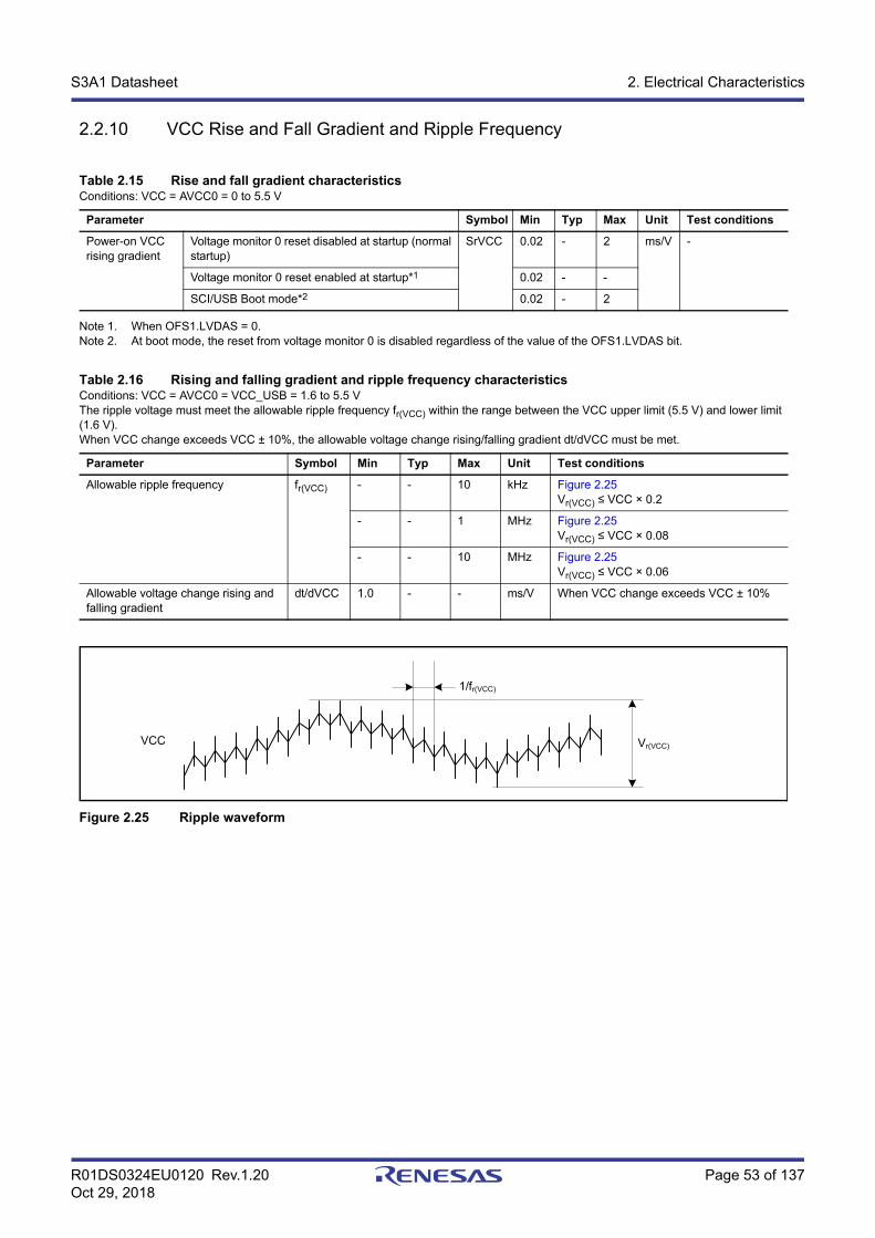
R01DS0324EU0120 Rev.1.20 Page 53 of 137Oct 29, 2018
S3A1 Datasheet 2. Electrical Characteristics
2.2.10 VCC Rise and Fall Gradient and Ripple Frequency
Note 1. When OFS1.LVDAS = 0.Note 2. At boot mode, the reset from voltage monitor 0 is disabled regardless of the value of the OFS1.LVDAS bit.
Figure 2.25 Ripple waveform
Table 2.15 Rise and fall gradient characteristicsConditions: VCC = AVCC0 = 0 to 5.5 V
Parameter Symbol Min Typ Max Unit Test conditions
Power-on VCC rising gradient
Voltage monitor 0 reset disabled at startup (normal startup)
SrVCC 0.02 - 2 ms/V -
Voltage monitor 0 reset enabled at startup*1 0.02 - -
SCI/USB Boot mode*2 0.02 - 2
Table 2.16 Rising and falling gradient and ripple frequency characteristicsConditions: VCC = AVCC0 = VCC_USB = 1.6 to 5.5 VThe ripple voltage must meet the allowable ripple frequency fr(VCC) within the range between the VCC upper limit (5.5 V) and lower limit (1.6 V). When VCC change exceeds VCC ± 10%, the allowable voltage change rising/falling gradient dt/dVCC must be met.
Parameter Symbol Min Typ Max Unit Test conditions
Allowable ripple frequency fr(VCC) - - 10 kHz Figure 2.25Vr(VCC) ≤ VCC × 0.2
- - 1 MHz Figure 2.25Vr(VCC) ≤ VCC × 0.08
- - 10 MHz Figure 2.25Vr(VCC) ≤ VCC × 0.06
Allowable voltage change rising and falling gradient
dt/dVCC 1.0 - - ms/V When VCC change exceeds VCC ± 10%
Vr(VCC)VCC
1/fr(VCC)
R01DS0324EU0120 Rev.1.20 Page 54 of 137Oct 29, 2018
S3A1 Datasheet 2. Electrical Characteristics
2.3 AC Characteristics
2.3.1 Frequency
Note 1. The lower-limit frequency of FCLK is 1 MHz while programming or erasing the flash memory. When using FCLK for programming or erasing the flash memory at below 4 MHz, the frequency can be set to 1 MHz, 2 MHz, or 3 MHz. A non-integer frequency such as 1.5 MHz cannot be set.
Note 2. The frequency accuracy of FCLK must be ±3.5% while programming or erasing the flash memory. Confirm the frequency accuracy of the clock source.
Note 3. The lower-limit frequency of PCLKC is 4 MHz at 2.4 V or above and 1 MHz at below 2.4 V when the 14-bit A/D converter is in use.
Note 4. See section 9, Clock Generation Circuit in User’s Manual for the relationship of frequencies between ICLK, PCLKA, PCLKB, PCLKC, PCLKD, FCLK, and BCLK.
Note 5. The maximum value of operation frequency does not include the internal oscillator errors. The operation can be guaranteed with the errors of the internal oscillator. For details on the range for guaranteed operation, see Table 2.22, Clock timing in User’s Manual.
Table 2.17 Operation frequency value in high-speed operating modeConditions: VCC = AVCC0 = 2.4 to 5.5 V
Parameter Symbol Min Typ Max*5 Unit
Operation frequency
System clock (ICLK)*4 2.7 to 5.5 V f 0.032768 - 48 MHz
2.4 to 2.7 V 0.032768 - 16
FlashIF clock (FCLK)*1, *2, *4 2.7 to 5.5 V 0.032768 - 32
2.4 to 2.7 V 0.032768 - 16
Peripheral module clock (PCLKA)*4 2.7 to 5.5 V - - 48
2.4 to 2.7 V - - 16
Peripheral module clock (PCLKB)*4 2.7 to 5.5 V - - 32
2.4 to 2.7 V - - 16
Peripheral module clock (PCLKC)*3, *4 2.7 to 5.5 V - - 64
2.4 to 2.7 V - - 16
Peripheral module clock (PCLKD)*4 2.7 to 5.5 V - - 64
2.4 to 2.7 V - - 16
External bus clock (BCLK)*4 2.7 to 5.5 V - - 24
2.4 to 2.7 V - - 16
EBCLK pin output 2.7 to 5.5 V - - 12
2.4 to 2.7 V - - 8
R01DS0324EU0120 Rev.1.20 Page 55 of 137Oct 29, 2018
S3A1 Datasheet 2. Electrical Characteristics
Note 1. The lower-limit frequency of FCLK is 1 MHz while programming or erasing the flash memory. When using FCLK for programming or erasing the flash memory at below 4 MHz, the frequency can be set to 1 MHz, 2 MHz, or 3 MHz. A non-integer frequency such as 1.5 MHz cannot be set.
Note 2. The frequency accuracy of FCLK must be ±3.5% while programming or erasing the flash memory. Confirm the frequency accuracy of the clock source.
Note 3. The lower-limit frequency of PCLKC is 4 MHz at 2.4 V or above and 1 MHz at below 2.4 V when the 14-bit A/D converter is in use.Note 4. See section 9, Clock Generation Circuit in User’s Manual for the relationship of frequencies between ICLK, PCLKA, PCLKB,
PCLKC, PCLKD, FCLK, and BCLK.Note 5. The maximum value of operation frequency does not include errors of the internal oscillator. The operation can be guaranteed
with errors of the internal oscillator. For details on the range for guaranteed operation, see Table 2.22, Clock timing.
Note 1. The lower-limit frequency of FCLK is 1 MHz while programming or erasing the flash memory.Note 2. The lower-limit frequency of PCLKC is 1 MHz when the A/D converter is in use.
Table 2.18 Operation frequency value in Middle-speed modeConditions: VCC = AVCC0 = 1.8 to 5.5 V
Parameter Symbol Min Typ Max*5 Unit
Operation frequency
System clock (ICLK)*4 2.7 to 5.5 V f 0.032768 - 12 MHz
2.4 to 2.7 V 0.032768 - 12
1.8 to 2.4 V 0.032768 - 8
FlashIF clock (FCLK)*1, *2, *4 2.7 to 5.5 V 0.032768 - 12
2.4 to 2.7 V 0.032768 - 12
1.8 to 2.4 V 0.032768 - 8
Peripheral module clock (PCLKA)*4 2.7 to 5.5 V - - 12
2.4 to 2.7 V - - 12
1.8 to 2.4 V - - 8
Peripheral module clock (PCLKB)*4 2.7 to 5.5 V - - 12
2.4 to 2.7 V - - 12
1.8 to 2.4 V - - 8
Peripheral module clock (PCLKC)*3, *4 2.7 to 5.5 V - - 12
2.4 to 2.7 V - - 12
1.8 to 2.4 V - - 8
Peripheral module clock (PCLKD)*4 2.7 to 5.5 V - - 12
2.4 to 2.7 V - - 12
1.8 to 2.4 V - - 8
External bus clock (BCLK)*4 2.7 to 5.5 V - - 12
2.4 to 2.7 V - - 12
1.8 to 2.4 V - - 8
EBCLK pin output 2.7 to 3.6 V - - 12
2.4 to 2.7 V - - 8
1.8 to 2.4 V - - 8
Table 2.19 Operation frequency value in Low-speed modeConditions: VCC = AVCC0 = 1.8 to 5.5 V
Parameter Symbol Min Typ Max*4 Unit
Operation frequency
System clock (ICLK)*3 1.8 to 5.5 V f 0.032768 - 1 MHz
FlashIF clock (FCLK)*1, *3 1.8 to 5.5 V 0.032768 - 1
Peripheral module clock (PCLKA)*3 1.8 to 5.5 V - - 1
Peripheral module clock (PCLKB)*3 1.8 to 5.5 V - - 1
Peripheral module clock (PCLKC)*2, *3 1.8 to 5.5 V - - 1
Peripheral module clock (PCLKD)*3 1.8 to 5.5 V - - 1
External bus clock (BCLK)*3 1.8 to 5.5 V - - 1
EBCLK pin output 1.8 to 5.5 V - - 1
R01DS0324EU0120 Rev.1.20 Page 56 of 137Oct 29, 2018
S3A1 Datasheet 2. Electrical Characteristics
Note 3. See section 9, Clock Generation Circuit in User’s Manual for the relationship of frequencies between ICLK, PCLKA, PCLKB, PCLKC, PCLKD, FCLK, and BCLK.
Note 4. The maximum value of operation frequency does not include the internal oscillator errors. The operation can be guaranteed with the errors of the internal oscillator. For details on the range for guaranteed operation, see Table 2.22, Clock timing.
Note 1. The lower-limit frequency of FCLK is 1 MHz while programming or erasing the flash memory. When using FCLK for programming or erasing the flash memory at below 4 MHz, the frequency can be set to 1 MHz, 2 MHz, or 3 MHz. A non-integer frequency such as 1.5 MHz cannot be set.
Note 2. The frequency accuracy of FCLK must be ±3.5% while programming or erasing the flash memory. Confirm the frequency accuracy of the clock source.
Note 3. The lower-limit frequency of PCLKC is 4 MHz at 2.4 V or above and 1 MHz at below 2.4 V when the 14-bit A/D converter is in use.
Note 4. See section 9, Clock Generation Circuit in User’s Manual for the relationship of frequencies between ICLK, PCLKA, PCLKB, PCLKC, PCLKD, FCLK, and BCLK.
Note 5. The maximum value of operation frequency does not include errors of the internal oscillator. The operation can be guaranteed with the errors of the internal oscillator. For details on the range for guaranteed operation, see Table 2.22, Clock timing.
Note 1. Programming and erasing the flash memory are not possible.Note 2. The 14-bit A/D converter cannot be used.Note 3. See section 9, Clock Generation Circuit in User’s Manual for the relationship of frequencies between ICLK, PCLKA, PCLKB,
PCLKC, PCLKD, FCLK, and BCLK.
Table 2.20 Operation frequency value in Low-voltage modeConditions: VCC = AVCC0 = 1.6 to 5.5 V
Parameter Symbol Min Typ Max*5 Unit
Operation frequency
System clock (ICLK)*4 1.6 to 5.5 V f 0.032768 - 4 MHz
FlashIF clock (FCLK)*1, *2, *4 1.6 to 5.5 V 0.032768 - 4
Peripheral module clock (PCLKA)*4 1.6 to 5.5 V - - 4
Peripheral module clock (PCLKB)*4 1.6 to 5.5 V - - 4
Peripheral module clock (PCLKC)*3, *4 1.6 to 5.5 V - - 4
Peripheral module clock (PCLKD)*4 1.6 to 5.5 V - - 4
External bus clock (BCLK)*4 1.6 to 5.5 V - - 4
EBCLK pin output 1.8 to 5.5 V - - 4
1.6 to 1.8 V - - 2
Table 2.21 Operation frequency value in Subosc-speed modeConditions: VCC = AVCC0 = 1.8 to 5.5 V
Parameter Symbol Min Typ Max Unit
Operation frequency
System clock (ICLK)*3 1.8 to 5.5 V f 27.8528 32.768 37.6832 kHz
FlashIF clock (FCLK)*1, *3 1.8 to 5.5 V 27.8528 32.768 37.6832
Peripheral module clock (PCLKA)*3 1.8 to 5.5 V - - 37.6832
Peripheral module clock (PCLKB)*3 1.8 to 5.5 V - - 37.6832
Peripheral module clock (PCLKC)*2, *3 1.8 to 5.5 V - - 37.6832
Peripheral module clock (PCLKD)*3 1.8 to 5.5 V - - 37.6832
External bus clock (BCLK)*3 1.8 to 5.5 V - - 37.6832
EBCLK pin output 1.8 to 5.5 V - - 37.6832
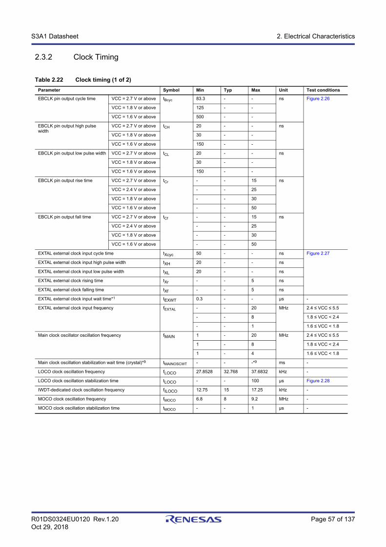
R01DS0324EU0120 Rev.1.20 Page 57 of 137Oct 29, 2018
S3A1 Datasheet 2. Electrical Characteristics
2.3.2 Clock Timing
Table 2.22 Clock timing (1 of 2)
Parameter Symbol Min Typ Max Unit Test conditions
EBCLK pin output cycle time VCC = 2.7 V or above tBcyc 83.3 - - ns Figure 2.26
VCC = 1.8 V or above 125 - -
VCC = 1.6 V or above 500 - -
EBCLK pin output high pulse width
VCC = 2.7 V or above tCH 20 - - ns
VCC = 1.8 V or above 30 - -
VCC = 1.6 V or above 150 - -
EBCLK pin output low pulse width VCC = 2.7 V or above tCL 20 - - ns
VCC = 1.8 V or above 30 - -
VCC = 1.6 V or above 150 - -
EBCLK pin output rise time VCC = 2.7 V or above tCr - - 15 ns
VCC = 2.4 V or above - - 25
VCC = 1.8 V or above - - 30
VCC = 1.6 V or above - - 50
EBCLK pin output fall time VCC = 2.7 V or above tCf - - 15 ns
VCC = 2.4 V or above - - 25
VCC = 1.8 V or above - - 30
VCC = 1.6 V or above - - 50
EXTAL external clock input cycle time tXcyc 50 - - ns Figure 2.27
EXTAL external clock input high pulse width tXH 20 - - ns
EXTAL external clock input low pulse width tXL 20 - - ns
EXTAL external clock rising time tXr - - 5 ns
EXTAL external clock falling time tXf - - 5 ns
EXTAL external clock input wait time*1 tEXWT 0.3 - - μs -
EXTAL external clock input frequency fEXTAL - - 20 MHz 2.4 ≤ VCC ≤ 5.5
- - 8 1.8 ≤ VCC < 2.4
- - 1 1.6 ≤ VCC < 1.8
Main clock oscillator oscillation frequency fMAIN 1 - 20 MHz 2.4 ≤ VCC ≤ 5.5
1 - 8 1.8 ≤ VCC < 2.4
1 - 4 1.6 ≤ VCC < 1.8
Main clock oscillation stabilization wait time (crystal)*9 tMAINOSCWT - - -*9 ms -
LOCO clock oscillation frequency fLOCO 27.8528 32.768 37.6832 kHz -
LOCO clock oscillation stabilization time tLOCO - - 100 μs Figure 2.28
IWDT-dedicated clock oscillation frequency fILOCO 12.75 15 17.25 kHz -
MOCO clock oscillation frequency fMOCO 6.8 8 9.2 MHz -
MOCO clock oscillation stabilization time tMOCO - - 1 μs -
R01DS0324EU0120 Rev.1.20 Page 58 of 137Oct 29, 2018
S3A1 Datasheet 2. Electrical Characteristics
Note 1. Time until the clock can be used after the Main Clock Oscillator Stop bit (MOSCCR.MOSTP) is set to 0 (operating) when the external clock is stable.
Note 2. The VCC range that the PLL can be used is 2.4 to 5.5 V.Note 3. After changing the setting of the SOSCCR.SOSTP bit so that the sub-clock oscillator operates, only start using the sub-clock
oscillator after the sub-clock oscillation stabilization wait time elapsed. Use the oscillator wait time recommended by the oscillator manufacturer.
Note 4. The 48-MHz HOCO can be used within a VCC range of 1.8 V to 5.5 V.Note 5. The 64-MHz HOCO can be used within a VCC range of 2.4 V to 5.5 V.Note 6. This is a characteristic when HOCOCR.HCSTP bit is set to 0 (oscillation) in MOCO stop state.
When HOCOCR.HCSTP bit is set to 0 (oscillation) during MOCO oscillation, this specification is shortened by 1 μs.Note 7. Whether stabilization time has elapsed can be confirmed by OSCSF.HOCOSF.Note 8. This is a characteristic when PLLCR.PLLSTP bit is set to 0 (operation) in MOCO stop state.
When PLLCR.PLLSTP bit is set to 0 (operation) during MOCO oscillation, this specification is shortened by 1 μs.Note 9. When setting up the main clock, ask the oscillator manufacturer for an oscillation evaluation and use the results as the
recommended oscillation stabilization time. Set the MOSCWTCR register to a value equal to or greater than the recommended stabilization time. After changing the setting of the MOSCCR.MOSTP bit so that the main clock oscillator operates, read the OSCSF.MOSCSF flag to confirm that it is 1, then start using the main clock.
HOCO clock oscillation frequency fHOCO24 23.64 24 24.36 MHz Ta = -40 to -20°C1.8 ≤ VCC ≤ 5.5
22.68 24 25.32 Ta = -40 to 85°C1.6 ≤ VCC < 1.8
23.76 24 24.24 Ta = -20 to 85°C1.8 ≤ VCC ≤ 5.5
23.52 24 24.48 Ta = 85 to 105°C2.4 ≤ VCC ≤ 5.5
fHOCO32 31.52 32 32.48 Ta = -40 to -20°C1.8 ≤ VCC ≤ 5.5
30.24 32 33.76 Ta = -40 to 85°C1.6 ≤ VCC < 1.8
31.68 32 32.32 Ta = -20 to 85°C1.8 ≤ VCC ≤ 5.5
31.36 32 32.64 Ta = 85 to 105°C2.4 ≤ VCC ≤ 5.5
fHOCO48*4 47.28 48 48.72 Ta = -40 to -20°C1.8 ≤ VCC ≤ 5.5
47.52 48 48.48 Ta = -20 to 85°C1.8 ≤ VCC ≤ 5.5
47.04 48 48.96 Ta = 85 to 105°C2.4 ≤ VCC ≤ 5.5
fHOCO64*5 63.04 64 64.96 Ta = -40 to -20°C2.4 ≤ VCC ≤ 5.5
63.36 64 64.64 Ta = -20 to 85°C2.4 ≤ VCC ≤ 5.5
62.72 64 65.28 Ta = 85 to 105°C2.4 ≤ VCC ≤ 5.5
HOCO clock oscillation stabilization time*6, *7
Except Low-voltage mode
tHOCO24tHOCO32
- - 37.1 μs Figure 2.29
tHOCO48 - - 43.3
tHOCO64 - - 80.6
Low-voltage mode tHOCO24tHOCO32tHOCO48tHOCO64
- - 100.9
PLL input frequency*2 fPLLIN 4 - 12.5 MHz -
PLL circuit oscillation frequency*2 fPLL 24 - 64 MHz -
PLL clock oscillation stabilization time*8 tPLL - - 55.5 μs Figure 2.31
PLL free-running oscillation frequency fPLLFR - 8 - MHz -
Sub-clock oscillator oscillation frequency fSUB - 32.768 - kHz -
Sub-clock oscillation stabilization time*3 tSUBOSC - - -*3 s Figure 2.32
Table 2.22 Clock timing (2 of 2)
Parameter Symbol Min Typ Max Unit Test conditions
R01DS0324EU0120 Rev.1.20 Page 59 of 137Oct 29, 2018
S3A1 Datasheet 2. Electrical Characteristics
Figure 2.26 EBCLK pin output timing
Figure 2.27 EXTAL external clock input timing
Figure 2.28 LOCO clock oscillation start timing
Figure 2.29 HOCO clock oscillation start timing (started by setting HOCOCR.HCSTP bit)
tCf
tCH
tBcyc
tCrtCL
EBCLK pin output
Test conditions: VOH = VCC × 0.7, VOL = VCC × 0.3, IOH = -1.0 mA, IOL = 1.0 mA, C = 30 pF
tXH
tXcyc
EXTAL external clock input VCC × 0.5
tXL
tXr tXf
LOCO clock oscillator output
LOCOCR.LCSTP
tLOCO
HOCO clock
HOCOCR.HCSTP
tHOCOx*1
Note 1. x = 24, 32, 48, 64
R01DS0324EU0120 Rev.1.20 Page 60 of 137Oct 29, 2018
S3A1 Datasheet 2. Electrical Characteristics
Figure 2.30 Main clock oscillation start timing
Figure 2.31 PLL clock oscillation start timing (PLL is operated after main clock oscillation has settled)
Figure 2.32 Sub-clock oscillation start timing
Figure 2.33 MOCO clock oscillation start timing
Main clock oscillator output
MOSCCR.MOSTP
Main clock
tMAINOSCWT
PLLCR.PLLSTP
PLL clock
tPLL
Sub-clock oscillator output
SOSCCR.SOSTP
tSUBOSC
MOCO clock oscillator output
MOCOCR.MCSTP
tMOCO
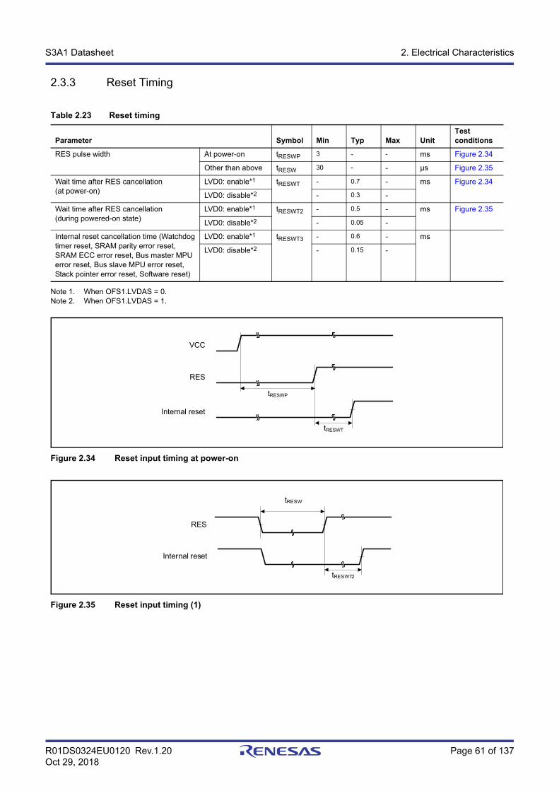
R01DS0324EU0120 Rev.1.20 Page 61 of 137Oct 29, 2018
S3A1 Datasheet 2. Electrical Characteristics
2.3.3 Reset Timing
Note 1. When OFS1.LVDAS = 0.Note 2. When OFS1.LVDAS = 1.
Figure 2.34 Reset input timing at power-on
Figure 2.35 Reset input timing (1)
Table 2.23 Reset timing
Parameter Symbol Min Typ Max UnitTest conditions
RES pulse width At power-on tRESWP 3 - - ms Figure 2.34
Other than above tRESW 30 - - μs Figure 2.35
Wait time after RES cancellation(at power-on)
LVD0: enable*1 tRESWT - 0.7 - ms Figure 2.34
LVD0: disable*2 - 0.3 -
Wait time after RES cancellation(during powered-on state)
LVD0: enable*1 tRESWT2 - 0.5 - ms Figure 2.35
LVD0: disable*2 - 0.05 -
Internal reset cancellation time (Watchdog timer reset, SRAM parity error reset, SRAM ECC error reset, Bus master MPU error reset, Bus slave MPU error reset, Stack pointer error reset, Software reset)
LVD0: enable*1 tRESWT3 - 0.6 - ms
LVD0: disable*2 - 0.15 -
VCC
RES
tRESWP
Internal reset
tRESWT
RES
Internal reset
tRESWT2
tRESW
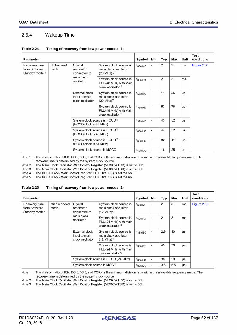
R01DS0324EU0120 Rev.1.20 Page 62 of 137Oct 29, 2018
S3A1 Datasheet 2. Electrical Characteristics
2.3.4 Wakeup Time
Note 1. The division ratio of ICK, BCK, FCK, and PCKx is the minimum division ratio within the allowable frequency range. The recovery time is determined by the system clock source.
Note 2. The Main Clock Oscillator Wait Control Register (MOSCWTCR) is set to 05h.Note 3. The Main Clock Oscillator Wait Control Register (MOSCWTCR) is set to 00h.Note 4. The HOCO Clock Wait Control Register (HOCOWTCR) is set to 05h.Note 5. The HOCO Clock Wait Control Register (HOCOWTCR) is set to 06h.
Note 1. The division ratio of ICK, BCK, FCK, and PCKx is the minimum division ratio within the allowable frequency range. The recovery time is determined by the system clock source.
Note 2. The Main Clock Oscillator Wait Control Register (MOSCWTCR) is set to 05h.Note 3. The Main Clock Oscillator Wait Control Register (MOSCWTCR) is set to 00h.
Table 2.24 Timing of recovery from low power modes (1)
Parameter Symbol Min Typ Max UnitTest conditions
Recovery time from Software Standby mode*1
High-speed mode
Crystal resonator connected to main clock oscillator
System clock source is main clock oscillator (20 MHz)*2
tSBYMC - 2 3 ms Figure 2.36
System clock source is PLL (48 MHz) with Main clock oscillator*2
tSBYPC - 2 3 ms
External clock input to main clock oscillator
System clock source is main clock oscillator (20 MHz)*3
tSBYEX - 14 25 μs
System clock source is PLL (48 MHz) with Main clock oscillator*3
tSBYPE - 53 76 μs
System clock source is HOCO*4 (HOCO clock is 32 MHz)
tSBYHO - 43 52 μs
System clock source is HOCO*4 (HOCO clock is 48 MHz)
tSBYHO - 44 52 μs
System clock source is HOCO*5
(HOCO clock is 64 MHz)tSBYHO - 82 110 μs
System clock source is MOCO tSBYMO - 16 25 μs
Table 2.25 Timing of recovery from low power modes (2)
Parameter Symbol Min Typ Max UnitTest conditions
Recovery time from Software Standby mode*1
Middle-speed mode
Crystal resonator connected to main clock oscillator
System clock source is main clock oscillator (12 MHz)*2
tSBYMC - 2 3 ms Figure 2.36
System clock source is PLL (24 MHz) with main clock oscillator*2
tSBYPC - 2 3 ms
External clock input to main clock oscillator
System clock source is main clock oscillator (12 MHz)*3
tSBYEX - 2.9 10 μs
System clock source is PLL (24 MHz) with main clock oscillator*3
tSBYPE - 49 76 μs
System clock source is HOCO (24 MHz) tSBYHO - 38 50 μs
System clock source is MOCO tSBYMO - 3.5 5.5 μs
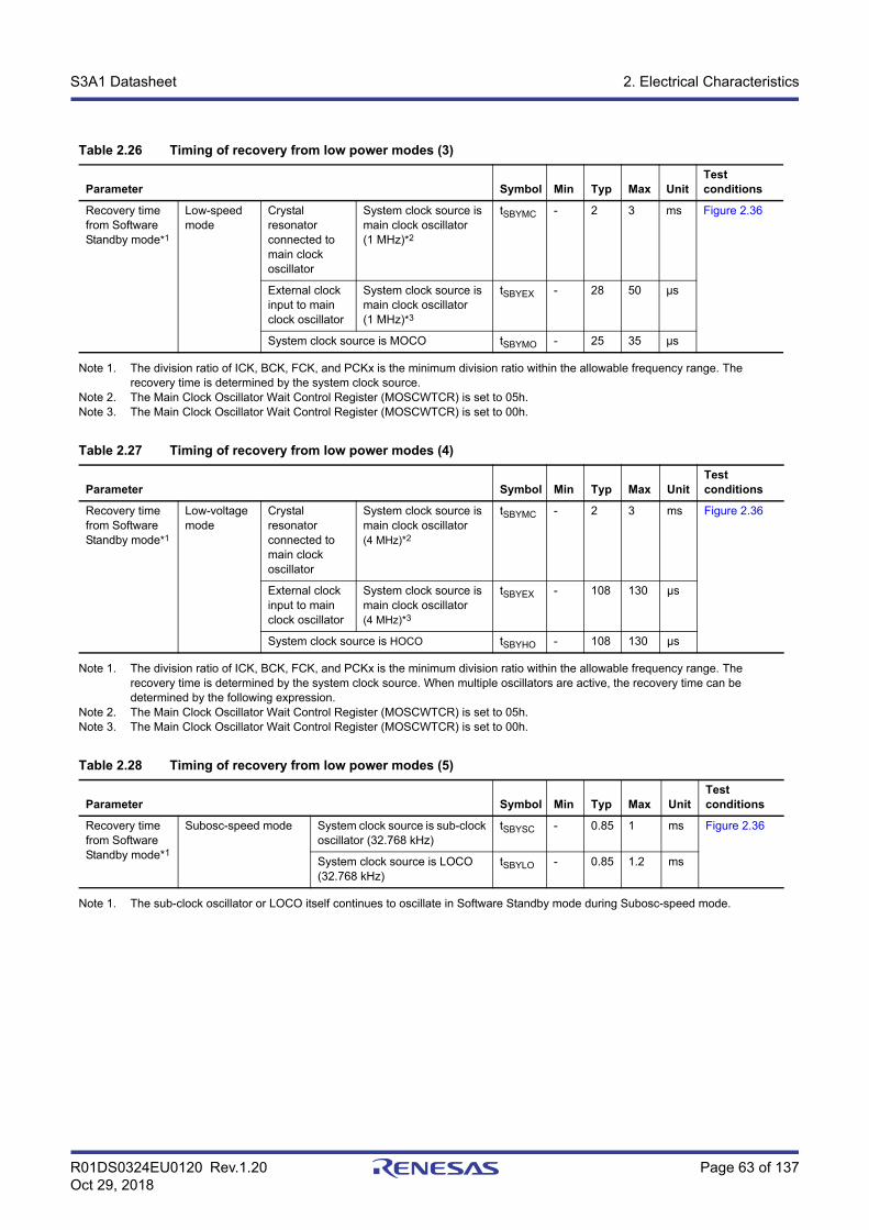
R01DS0324EU0120 Rev.1.20 Page 63 of 137Oct 29, 2018
S3A1 Datasheet 2. Electrical Characteristics
Note 1. The division ratio of ICK, BCK, FCK, and PCKx is the minimum division ratio within the allowable frequency range. The recovery time is determined by the system clock source.
Note 2. The Main Clock Oscillator Wait Control Register (MOSCWTCR) is set to 05h.Note 3. The Main Clock Oscillator Wait Control Register (MOSCWTCR) is set to 00h.
Note 1. The division ratio of ICK, BCK, FCK, and PCKx is the minimum division ratio within the allowable frequency range. The recovery time is determined by the system clock source. When multiple oscillators are active, the recovery time can be determined by the following expression.
Note 2. The Main Clock Oscillator Wait Control Register (MOSCWTCR) is set to 05h.Note 3. The Main Clock Oscillator Wait Control Register (MOSCWTCR) is set to 00h.
Note 1. The sub-clock oscillator or LOCO itself continues to oscillate in Software Standby mode during Subosc-speed mode.
Table 2.26 Timing of recovery from low power modes (3)
Parameter Symbol Min Typ Max UnitTest conditions
Recovery time from Software Standby mode*1
Low-speed mode
Crystal resonator connected to main clock oscillator
System clock source is main clock oscillator (1 MHz)*2
tSBYMC - 2 3 ms Figure 2.36
External clock input to main clock oscillator
System clock source is main clock oscillator (1 MHz)*3
tSBYEX - 28 50 μs
System clock source is MOCO tSBYMO - 25 35 μs
Table 2.27 Timing of recovery from low power modes (4)
Parameter Symbol Min Typ Max UnitTest conditions
Recovery time from Software Standby mode*1
Low-voltage mode
Crystal resonator connected to main clock oscillator
System clock source is main clock oscillator(4 MHz)*2
tSBYMC - 2 3 ms Figure 2.36
External clock input to main clock oscillator
System clock source is main clock oscillator(4 MHz)*3
tSBYEX - 108 130 μs
System clock source is HOCO tSBYHO - 108 130 μs
Table 2.28 Timing of recovery from low power modes (5)
Parameter Symbol Min Typ Max UnitTest conditions
Recovery time from Software Standby mode*1
Subosc-speed mode System clock source is sub-clock oscillator (32.768 kHz)
tSBYSC - 0.85 1 ms Figure 2.36
System clock source is LOCO (32.768 kHz)
tSBYLO - 0.85 1.2 ms
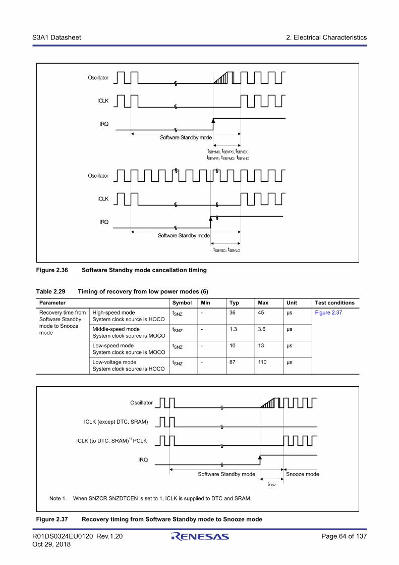
R01DS0324EU0120 Rev.1.20 Page 64 of 137Oct 29, 2018
S3A1 Datasheet 2. Electrical Characteristics
Figure 2.36 Software Standby mode cancellation timing
Figure 2.37 Recovery timing from Software Standby mode to Snooze mode
Table 2.29 Timing of recovery from low power modes (6)
Parameter Symbol Min Typ Max Unit Test conditions
Recovery time from Software Standby mode to Snooze mode
High-speed modeSystem clock source is HOCO
tSNZ - 36 45 μs Figure 2.37
Middle-speed modeSystem clock source is MOCO
tSNZ - 1.3 3.6 μs
Low-speed modeSystem clock source is MOCO
tSNZ - 10 13 μs
Low-voltage modeSystem clock source is HOCO
tSNZ - 87 110 μs
Oscillator
ICLK
IRQ
Software Standby mode
tSBYSC, tSBYLO
Oscillator
ICLK
IRQ
Software Standby mode
tSBYMC, tSBYPC, tSBYEX,
tSBYPE, tSBYMO, tSBYHO
Note 1. When SNZCR.SNZDTCEN is set to 1, ICLK is supplied to DTC and SRAM.
tSNZ
IRQ
ICLK (to DTC, SRAM)*1 PCLK
ICLK (except DTC, SRAM)
Oscillator
Software Standby mode Snooze mode
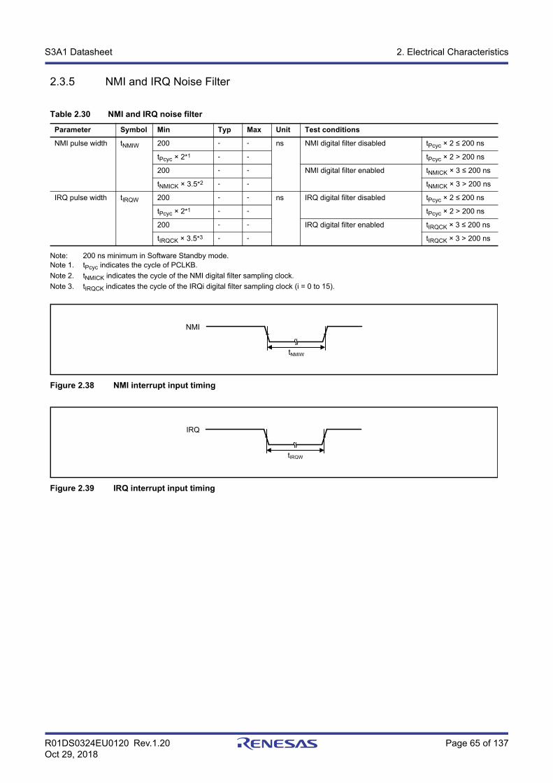
R01DS0324EU0120 Rev.1.20 Page 65 of 137Oct 29, 2018
S3A1 Datasheet 2. Electrical Characteristics
2.3.5 NMI and IRQ Noise Filter
Note: 200 ns minimum in Software Standby mode.Note 1. tPcyc indicates the cycle of PCLKB.
Note 2. tNMICK indicates the cycle of the NMI digital filter sampling clock.
Note 3. tIRQCK indicates the cycle of the IRQi digital filter sampling clock (i = 0 to 15).
Figure 2.38 NMI interrupt input timing
Figure 2.39 IRQ interrupt input timing
Table 2.30 NMI and IRQ noise filter
Parameter Symbol Min Typ Max Unit Test conditions
NMI pulse width tNMIW 200 - - ns NMI digital filter disabled tPcyc × 2 ≤ 200 ns
tPcyc × 2*1 - - tPcyc × 2 > 200 ns
200 - - NMI digital filter enabled tNMICK × 3 ≤ 200 ns
tNMICK × 3.5*2 - - tNMICK × 3 > 200 ns
IRQ pulse width tIRQW 200 - - ns IRQ digital filter disabled tPcyc × 2 ≤ 200 ns
tPcyc × 2*1 - - tPcyc × 2 > 200 ns
200 - - IRQ digital filter enabled tIRQCK × 3 ≤ 200 ns
tIRQCK × 3.5*3 - - tIRQCK × 3 > 200 ns
tNMIW
NMI
tIRQW
IRQ
R01DS0324EU0120 Rev.1.20 Page 66 of 137Oct 29, 2018
S3A1 Datasheet 2. Electrical Characteristics
2.3.6 Bus Timing
Table 2.31 Bus timing (1)Conditions: Low drive output is selected in the Port Drive Capability in PmnPFS registerVCC = 2.7 to 5.5 VOutput load conditions: VOH = VCC × 0.5, VOL = VCC × 0.5, C = 30 pF
Parameter Symbol Min Max Unit Test conditions
Address delay tAD - 55 ns Figure 2.42to Figure 2.45Byte control delay tBCD - 55 ns
CS delay tCSD - 55 ns
ALE delay time tALED - 55 ns
RD delay tRSD - 55 ns
Read data setup time tRDS 37 - ns
Read data hold time tRDH 0 - ns
WR delay tWRD - 55 ns
Write data delay tWDD - 55 ns
Write data hold time tWDH 0 - ns
WAIT setup time tWTS 37 - ns Figure 2.46
WAIT hold time tWTH 0 - ns
Table 2.32 Bus timing (2)Conditions: Low drive output is selected in the Port Drive Capability in PmnPFS registerVCC = 2.4 to 2.7 VOutput load conditions: VOH = VCC × 0.5, VOL = VCC × 0.5, C = 30 pF
Parameter Symbol Min Max Unit Test conditions
Address delay tAD - 55 ns Figure 2.42to Figure 2.45Byte control delay tBCD - 55 ns
CS delay tCSD - 55 ns
ALE delay time tALED - 55 ns
RD delay tRSD - 55 ns
Read data setup time tRDS 45 - ns
Read data hold time tRDH 0 - ns
WR delay tWRD - 55 ns
Write data delay tWDD - 55 ns
Write data hold time tWDH 0 - ns
WAIT setup time tWTS 45 - ns Figure 2.46
WAIT hold time tWTH 0 - ns
R01DS0324EU0120 Rev.1.20 Page 67 of 137Oct 29, 2018
S3A1 Datasheet 2. Electrical Characteristics
Table 2.33 Bus timing (3)Conditions: Low drive output is selected in the Port Drive Capability in PmnPFS registerVCC = 1.8 to 2.4 VOutput load conditions: VOH = VCC × 0.5, VOL = VCC × 0.5, C = 30 pF
Parameter Symbol Min Max Unit Test conditions
Address delay tAD - 90 ns Figure 2.42to Figure 2.45Byte control delay tBCD - 90 ns
CS delay tCSD - 90 ns
ALE delay time tALED - 90 ns
RD delay tRSD - 90 ns
Read data setup time tRDS 70 - ns
Read data hold time tRDH 0 - ns
WR delay tWRD - 90 ns
Write data delay tWDD - 90 ns
Write data hold time tWDH 0 - ns
WAIT setup time tWTS 70 - ns Figure 2.46
WAIT hold time tWTH 0 - ns
Table 2.34 Bus timing (4)Conditions: Low drive output is selected in the Port Drive Capability in PmnPFS registerVCC = 1.6 to 1.8 VOutput load conditions: VOH = VCC × 0.5, VOL = VCC × 0.5, C = 30 pF
Parameter Symbol Min Max Unit Test conditions
Address delay tAD - 120 ns Figure 2.42to Figure 2.45Byte control delay tBCD - 120 ns
CS delay tCSD - 120 ns
ALE delay time tALED - 120 ns
RD delay tRSD - 120 ns
Read data setup time tRDS 90 - ns
Read data hold time tRDH 0 - ns
WR delay tWRD - 120 ns
Write data delay tWDD - 120 ns
Write data hold time tWDH 0 - ns
WAIT setup time tWTS 90 - ns Figure 2.46
WAIT hold time tWTH 0 - ns
R01DS0324EU0120 Rev.1.20 Page 68 of 137Oct 29, 2018
S3A1 Datasheet 2. Electrical Characteristics
Figure 2.40 Address/data multiplexed bus read access timing
Figure 2.41 Address/data multiplexed bus write access timing
A15/D15 to A00/D00 (Read)
RD (Read)
tAD
EBCLK
A23 to A00
ALE
CS3 to CS0
tALED
TW1 TW2 Tn1
tAD tADtRDS
Tn2
tRSD tRSD
TW3 TW4 TW5 Tend
Ta1 Ta1 Tan
Address cycle Data cycle
tRDH
tALED
tCSDtCSD
A15/D15 to A00/D00 (Write)
WR1, WR0, WR (Write)
tAD
EBCLK
A23 to A00
ALE
CS3 to CS0
tALED
TW1 TW2 Tn1
tAD tAD
Tn2
tWRD tWRD
TW3 TW4 TW5 Tend
Ta1 Ta1 Tan
Address cycle Data cycle
tALED
tCSDtCSD
tWDD tWDH
Tn3
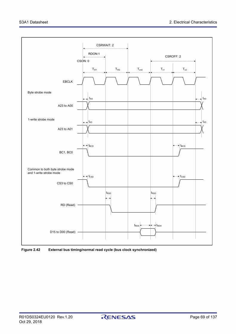
R01DS0324EU0120 Rev.1.20 Page 69 of 137Oct 29, 2018
S3A1 Datasheet 2. Electrical Characteristics
Figure 2.42 External bus timing/normal read cycle (bus clock synchronized)
A23 to A01
CS3 to CS0
tAD
EBCLK
A23 to A00
D15 to D00 (Read)
Byte strobe mode
1-write strobe mode
BC1, BC0
Common to both byte strobe mode and 1-write strobe mode
tBCD
tCSD tCSD
RD (Read)
tRSD tRSD
tAD
tRDHtRDS
tAD
tAD
tBCD
TW1 TW2 Tend Tn1 Tn2
RDON:1
CSRWAIT: 2
CSROFF: 2
CSON: 0
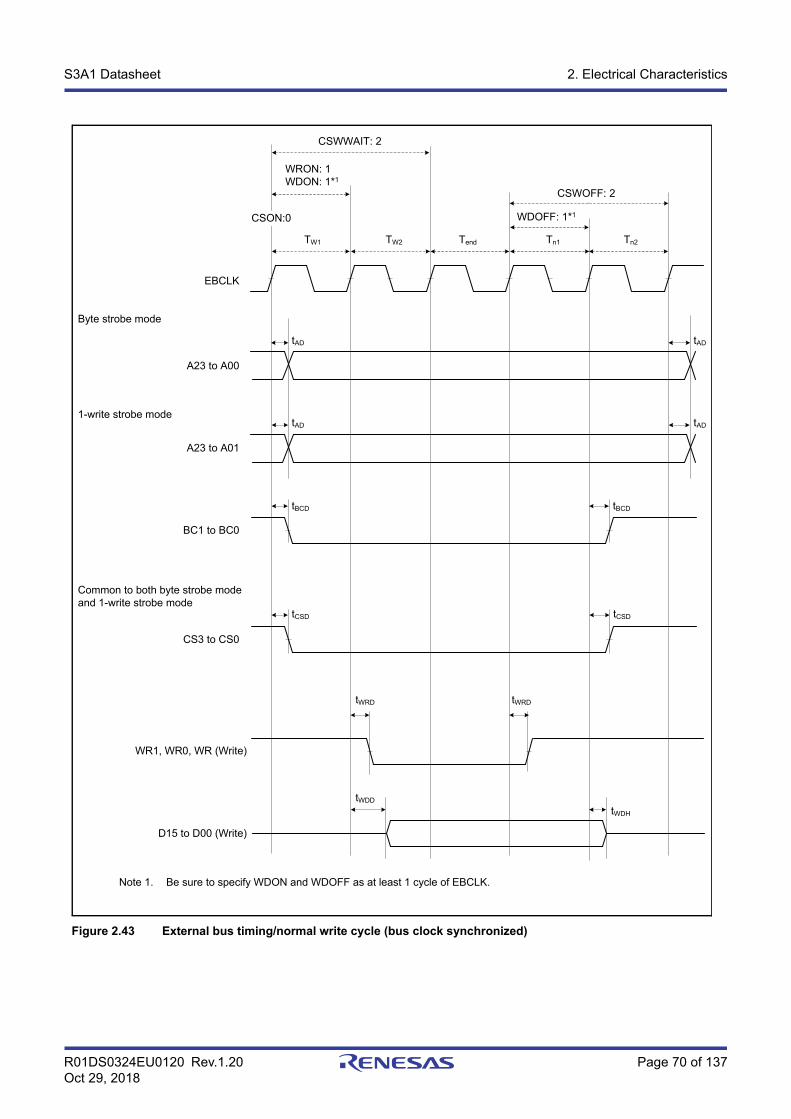
R01DS0324EU0120 Rev.1.20 Page 70 of 137Oct 29, 2018
S3A1 Datasheet 2. Electrical Characteristics
Figure 2.43 External bus timing/normal write cycle (bus clock synchronized)
Note 1. Be sure to specify WDON and WDOFF as at least 1 cycle of EBCLK.
A23 to A01
CS3 to CS0
tAD
EBCLK
A23 to A00
Byte strobe mode
1-write strobe mode
BC1 to BC0
Common to both byte strobe mode and 1-write strobe mode
tBCD
tCSD tCSD
tAD
tAD
tAD
tBCD
D15 to D00 (Write)
WR1, WR0, WR (Write)
tWRD tWRD
tWDH
tWDD
TW1 TW2 Tend Tn1 Tn2
WRON: 1WDON: 1*1
CSWWAIT: 2
WDOFF: 1*1CSON:0
CSWOFF: 2
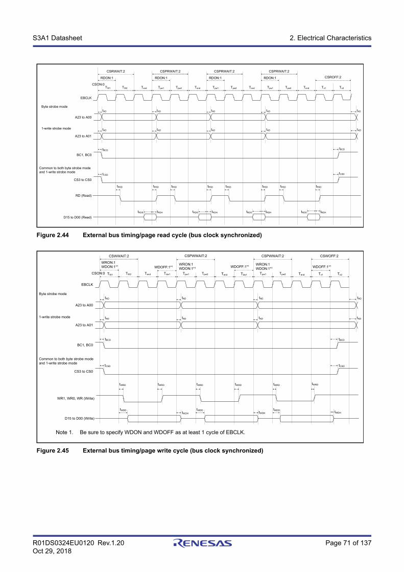
R01DS0324EU0120 Rev.1.20 Page 71 of 137Oct 29, 2018
S3A1 Datasheet 2. Electrical Characteristics
Figure 2.44 External bus timing/page read cycle (bus clock synchronized)
Figure 2.45 External bus timing/page write cycle (bus clock synchronized)
A23 to A01
CS3 to CS0
tAD
EBCLK
A23 to A00
D15 to D00 (Read)
Byte strobe mode
1-write strobe mode
BC1, BC0
Common to both byte strobe mode and 1-write strobe mode
tBCD
tCSDtCSD
RD (Read)
tRSD tRSD
tRDHtRDS
tAD
tBCD
TW1 TW2 Tend Tpw1 Tpw2
tAD tAD
tRSD tRSD
tRDHtRDS
tRSD tRSD
tRDHtRDS
Tend Tpw1 Tpw2 Tend Tn1 Tn2
tAD tAD tAD tAD
RDON:1
CSRWAIT:2
CSROFF:2
tRSD tRSD
tRDHtRDS
tAD
tAD
CSPRWAIT:2
Tpw1 Tpw2 Tend
RDON:1
CSPRWAIT:2
RDON:1
CSPRWAIT:2
RDON:1
CSON:0
A23 to A01
CS3 to CS0
tAD
EBCLK
A23 to A00
Byte strobe mode
1-write strobe mode
BC1, BC0
Common to both byte strobe mode and 1-write strobe mode
tBCD
tCSD tCSD
tAD
tBCD
TW1
D15 to D00 (Write)
WR1, WR0, WR (Write)
tWRD tWRD
tWDH
tWDD
TW2 Tend Tpw1 Tpw2
tAD tAD
tWRD tWRD
tWDH
tWDD
tWRD tWRD
tWDHtWDD
Tdw1 Tend Tpw1 Tpw2 Tend Tn1 Tn2Tdw1
tAD tAD tAD tAD
WRON:1WDON:1*1
CSWWAIT:2 CSPWWAIT:2
WDOFF:1*1
CSPWWAIT:2
WDOFF:1*1 WDOFF:1*1
CSON:0
WRON:1WDON:1*1
WRON:1WDON:1*1
CSWOFF:2
Note 1. Be sure to specify WDON and WDOFF as at least 1 cycle of EBCLK.
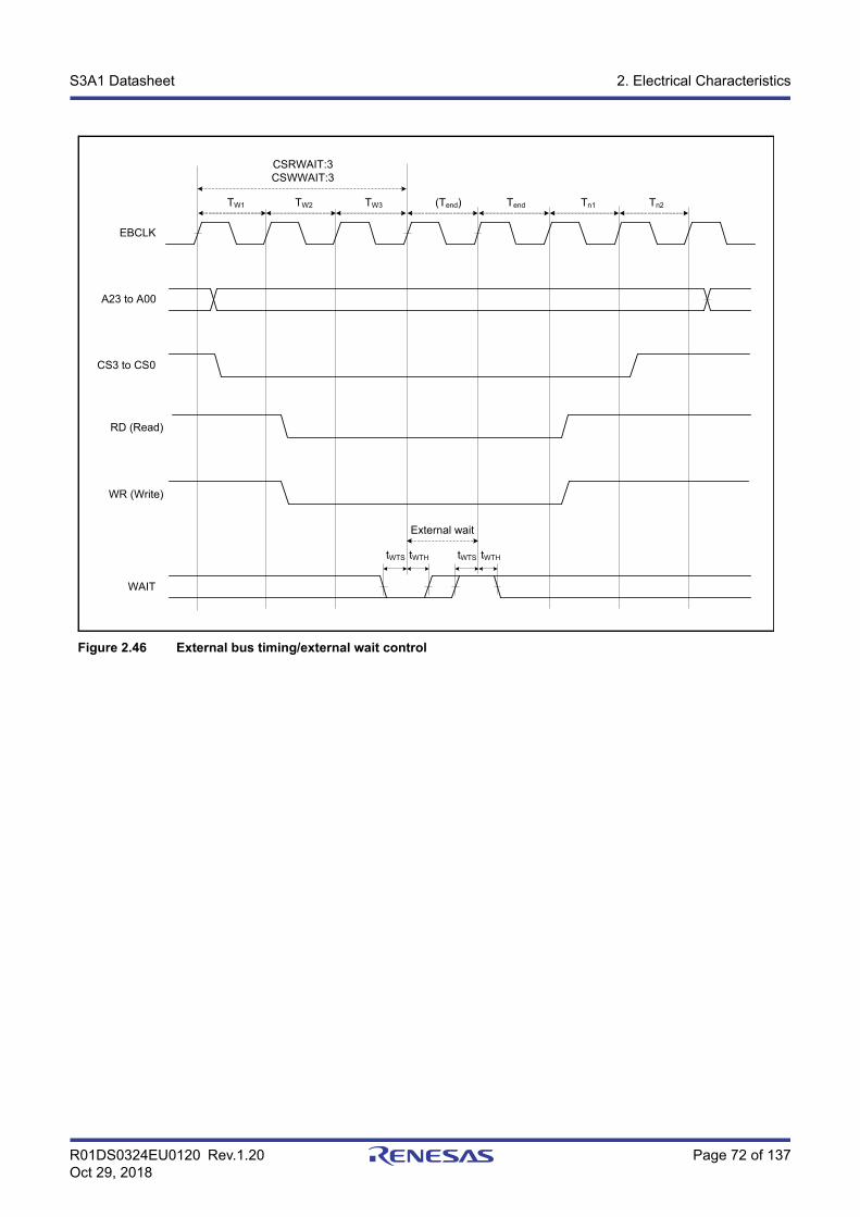
R01DS0324EU0120 Rev.1.20 Page 72 of 137Oct 29, 2018
S3A1 Datasheet 2. Electrical Characteristics
Figure 2.46 External bus timing/external wait control
tWTS tWTH tWTS tWTH
CSRWAIT:3CSWWAIT:3
EBCLK
A23 to A00
CS3 to CS0
RD (Read)
WR (Write)
WAIT
TW1 TW2 (Tend) TendTW3 Tn1 Tn2
External wait
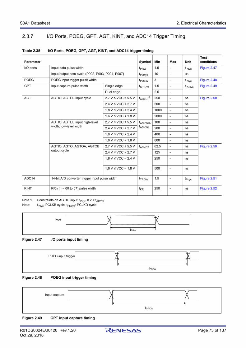
R01DS0324EU0120 Rev.1.20 Page 73 of 137Oct 29, 2018
S3A1 Datasheet 2. Electrical Characteristics
2.3.7 I/O Ports, POEG, GPT, AGT, KINT, and ADC14 Trigger Timing
Note 1. Constraints on AGTIO input: tPcyc × 2 < tACYC
Note: tPcyc: PCLKB cycle, tPDcyc: PCLKD cycle
Figure 2.47 I/O ports input timing
Figure 2.48 POEG input trigger timing
Figure 2.49 GPT input capture timing
Table 2.35 I/O Ports, POEG, GPT, AGT, KINT, and ADC14 trigger timing
Parameter Symbol Min Max UnitTest conditions
I/O ports Input data pulse width tPRW 1.5 - tPcyc Figure 2.47
Input/output data cycle (P002, P003, P004, P007) tPOcyc 10 - us
POEG POEG input trigger pulse width tPOEW 3 - tPcyc Figure 2.48
GPT Input capture pulse width Single edge tGTICW 1.5 - tPDcyc Figure 2.49
Dual edge 2.5 -
AGT AGTIO, AGTEE input cycle 2.7 V ≤ VCC ≤ 5.5 V tACYC*1 250 - ns Figure 2.50
2.4 V ≤ VCC < 2.7 V 500 - ns
1.8 V ≤ VCC < 2.4 V 1000 - ns
1.6 V ≤ VCC < 1.8 V 2000 - ns
AGTIO, AGTEE input high-level width, low-level width
2.7 V ≤ VCC ≤ 5.5 V tACKWH, tACKWL
100 - ns
2.4 V ≤ VCC < 2.7 V 200 - ns
1.8 V ≤ VCC < 2.4 V 400 - ns
1.6 V ≤ VCC < 1.8 V 800 - ns
AGTIO, AGTO, AGTOA, AGTOB output cycle
2.7 V ≤ VCC ≤ 5.5 V tACYC2 62.5 - ns Figure 2.50
2.4 V ≤ VCC < 2.7 V 125 - ns
1.8 V ≤ VCC < 2.4 V 250 - ns
1.6 V ≤ VCC < 1.8 V 500 - ns
ADC14 14-bit A/D converter trigger input pulse width tTRGW 1.5 - tPcyc Figure 2.51
KINT KRn (n = 00 to 07) pulse width tKR 250 - ns Figure 2.52
Port
tPRW
POEG input trigger
tPOEW
Input capture
tGTICW
R01DS0324EU0120 Rev.1.20 Page 74 of 137Oct 29, 2018
S3A1 Datasheet 2. Electrical Characteristics
Figure 2.50 AGT I/O timing
Figure 2.51 ADC14 trigger input timing
Figure 2.52 Key interrupt input timing
2.3.8 CAC Timing
Note 1. tPBcyc: PCLKB cycle.
Note 2. tcac: CAC count clock source cycle.
Table 2.36 CAC timing
Parameter Symbol Min Typ Max UnitTest conditions
CAC CACREF input pulse width tPBcyc*1 ≤ tcac*2 tCACREF 4.5 × tcac + 3 × tPBcyc*1 - - ns -
tPBcyc*1 > tcac*2 5 × tcac + 6.5 × tPBcyc*1 - - ns
tACYC2
AGTIO, AGTEE(input)
tACYC
tACKWL tACKWH
AGTIO, AGTO,AGTOA, AGTOB(output)
ADTRG0
tTRGW
KR00 to KR07
tKR
R01DS0324EU0120 Rev.1.20 Page 75 of 137Oct 29, 2018
S3A1 Datasheet 2. Electrical Characteristics
2.3.9 SCI Timing
Note 1. tPcyc: PCLKA cycle.
Figure 2.53 SCK clock input timing
Table 2.37 SCI timing (1)
Parameter Symbol Min Max Unit*1Test conditions
SCI Input clock cycle Asynchronous tScyc 4 - tPcyc Figure 2.53
Clock synchronous 6 -
Input clock pulse width tSCKW 0.4 0.6 tScyc
Input clock rise time tSCKr - 20 ns
Input clock fall time tSCKf - 20 ns
Output clock cycle Asynchronous tScyc 6 - tPcyc
Clock synchronous 4 -
Output clock pulse width tSCKW 0.4 0.6 tScyc
Output clock rise time 1.8 V or above tSCKr - 20 ns
1.6 V or above - 30
Output clock fall time 1.8 V or above tSCKf - 20 ns
1.6 V or above - 30
Transmit data delay (master)
Clock synchronous
1.8 V or above tTXD - 40 ns Figure 2.54
1.6 V or above - 45
Transmit data delay (slave)
Clock synchronous
2.7 V or above - 55 ns
2.4 V or above - 60
1.8 V or above - 100
1.6 V or above - 125
Receive data setup time (master)
Clock synchronous
2.7 V or above tRXS 45 - ns
2.4 V or above 55 -
1.8 V or above 90 -
1.6 V or above 110 -
Receive data setup time (slave)
Clock synchronous
2.7 V or above 40 - ns
1.6 V or above 45 -
Receive data hold time (master)
Clock synchronous tRXH 5 - ns
Receive data hold time (slave)
Clock synchronous tRXH 40 - ns
tSCKW tSCKr tSCKf
tScyc
SCKn(n = 0 to 4, 9)
R01DS0324EU0120 Rev.1.20 Page 76 of 137Oct 29, 2018
S3A1 Datasheet 2. Electrical Characteristics
Figure 2.54 SCI input/output timing in clock synchronous mode
Table 2.38 SCI timing (2) (1 of 2)
Parameter Symbol Min Max Unit Test conditions
Simple SPI
SCK clock cycle output (master) tSPcyc 4 65,536 tPcyc Figure 2.55
SCK clock cycle input (slave) 6 65,536
SCK clock high pulse width tSPCKWH 0.4 0.6 tSPcyc
SCK clock low pulse width tSPCKWL 0.4 0.6 tSPcyc
SCK clock rise and fall time 1.8 V or above tSPCKr, tSPCKf
- 20 ns
1.6 V or above - 30
Data input setup time
Master 2.7 V or above tSU 45 - ns Figure 2.56 to Figure 2.592.4 V or above 55 -
1.8 V or above 80 -
1.6 V or above 110 -
Slave 2.7 V or above 40 -
1.6 V or above 45 -
Data input hold time Master tH 33.3 - ns
Slave 40 -
SS input setup time tLEAD 1 - tSPcyc
SS input hold time tLAG 1 - tSPcyc
Data output delay Master 1.8 V or above tOD - 40 ns
1.6 V or above - 50
Slave 2.4 V or above - 65
1.8 V or above - 100
1.6 V or above - 125
Data output hold time
Master 2.7 V or above tOH -10 - ns
2.4 V or above -20 -
1.8 V or above -30 -
1.6 V or above -40 -
Slave -10 -
Data rise and fall time
Master 1.8 V or above tDr, tDf - 20 ns
1.6 V or above - 30
Slave 1.8 V or above - 20
1.6 V or above - 30
tTXD
tRXS tRXH
TXDn
RXDn
SCKn
n = 0 to 4, 9
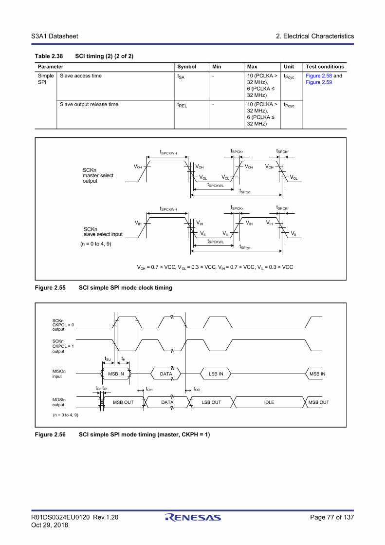
R01DS0324EU0120 Rev.1.20 Page 77 of 137Oct 29, 2018
S3A1 Datasheet 2. Electrical Characteristics
Figure 2.55 SCI simple SPI mode clock timing
Figure 2.56 SCI simple SPI mode timing (master, CKPH = 1)
Simple SPI
Slave access time tSA - 10 (PCLKA > 32 MHz),6 (PCLKA ≤ 32 MHz)
tPcyc Figure 2.58 and Figure 2.59
Slave output release time tREL - 10 (PCLKA > 32 MHz),6 (PCLKA ≤ 32 MHz)
tPcyc
Table 2.38 SCI timing (2) (2 of 2)
Parameter Symbol Min Max Unit Test conditions
tSPCKWH
VOH VOH
VOL VOL
VOH VOH
tSPCKWL
tSPCKr tSPCKf
VOL
tSPcyc
tSPCKWH
VIH VIH
VIL VIL
VIH VIH
tSPCKWL
tSPCKr tSPCKf
VIL
tSPcyc
VOH = 0.7 × VCC, VOL = 0.3 × VCC, VIH = 0.7 × VCC, VIL = 0.3 × VCC
(n = 0 to 4, 9)
SCKnmaster select output
SCKnslave select input
tDr, tDf
tSU tH
tOH tOD
MSB IN DATA LSB IN MSB IN
MSB OUT DATA LSB OUT IDLE MSB OUT
SCKnCKPOL = 0output
SCKnCKPOL = 1output
MISOninput
MOSInoutput
(n = 0 to 4, 9)
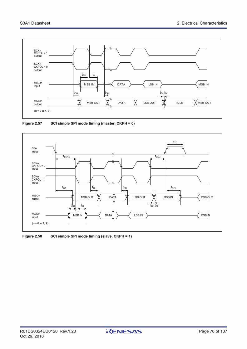
R01DS0324EU0120 Rev.1.20 Page 78 of 137Oct 29, 2018
S3A1 Datasheet 2. Electrical Characteristics
Figure 2.57 SCI simple SPI mode timing (master, CKPH = 0)
Figure 2.58 SCI simple SPI mode timing (slave, CKPH = 1)
tSU tH
tOH tOD
MSB IN DATA LSB IN MSB IN
MSB OUT DATA LSB OUT IDLE MSB OUT
SCKnCKPOL= 1output
SCKnCKPOL= 0output
MISOninput
MOSInoutput
(n = 0 to 4, 9)
tDr, tDf
tDr, tDftSU tH
tLEAD
tTD
tLAG
tSA
MSB IN DATA LSB IN MSB IN
MSB OUT DATA LSB OUT MSB IN MSB OUT
tOH tOD tREL
SSninput
SCKnCKPOL= 0input
SCKnCKPOL= 1input
MISOnoutput
MOSIninput
(n = 0 to 4, 9)
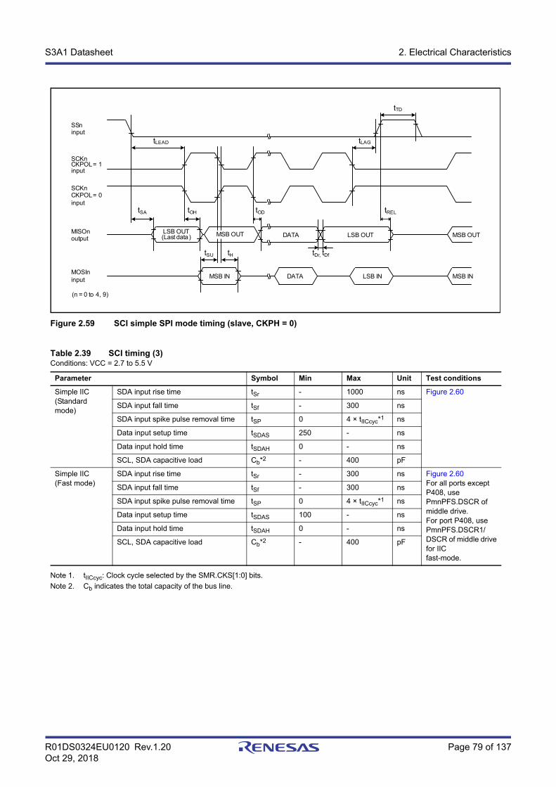
R01DS0324EU0120 Rev.1.20 Page 79 of 137Oct 29, 2018
S3A1 Datasheet 2. Electrical Characteristics
Figure 2.59 SCI simple SPI mode timing (slave, CKPH = 0)
Note 1. tIICcyc: Clock cycle selected by the SMR.CKS[1:0] bits.
Note 2. Cb indicates the total capacity of the bus line.
Table 2.39 SCI timing (3)Conditions: VCC = 2.7 to 5.5 V
Parameter Symbol Min Max Unit Test conditions
Simple IIC(Standard mode)
SDA input rise time tSr - 1000 ns Figure 2.60
SDA input fall time tSf - 300 ns
SDA input spike pulse removal time tSP 0 4 × tIICcyc*1 ns
Data input setup time tSDAS 250 - ns
Data input hold time tSDAH 0 - ns
SCL, SDA capacitive load Cb*2 - 400 pF
Simple IIC(Fast mode)
SDA input rise time tSr - 300 ns Figure 2.60For all ports except P408, use PmnPFS.DSCR of middle drive.For port P408, use PmnPFS.DSCR1/DSCR of middle drive for IIC fast-mode.
SDA input fall time tSf - 300 ns
SDA input spike pulse removal time tSP 0 4 × tIICcyc*1 ns
Data input setup time tSDAS 100 - ns
Data input hold time tSDAH 0 - ns
SCL, SDA capacitive load Cb*2 - 400 pF
tDr, tDf
tSA tOH
tLEAD
tTD
tLAG
tH
LSB OUT(Last data) DATA MSB OUT
MSB IN DATA LSB IN MSB IN
LSB OUT
tSU
tOD tREL
MSB OUT
SSninput
SCKnCKPOL= 1input
SCKnCKPOL= 0input
MISOnoutput
MOSIninput
(n = 0 to 4, 9)
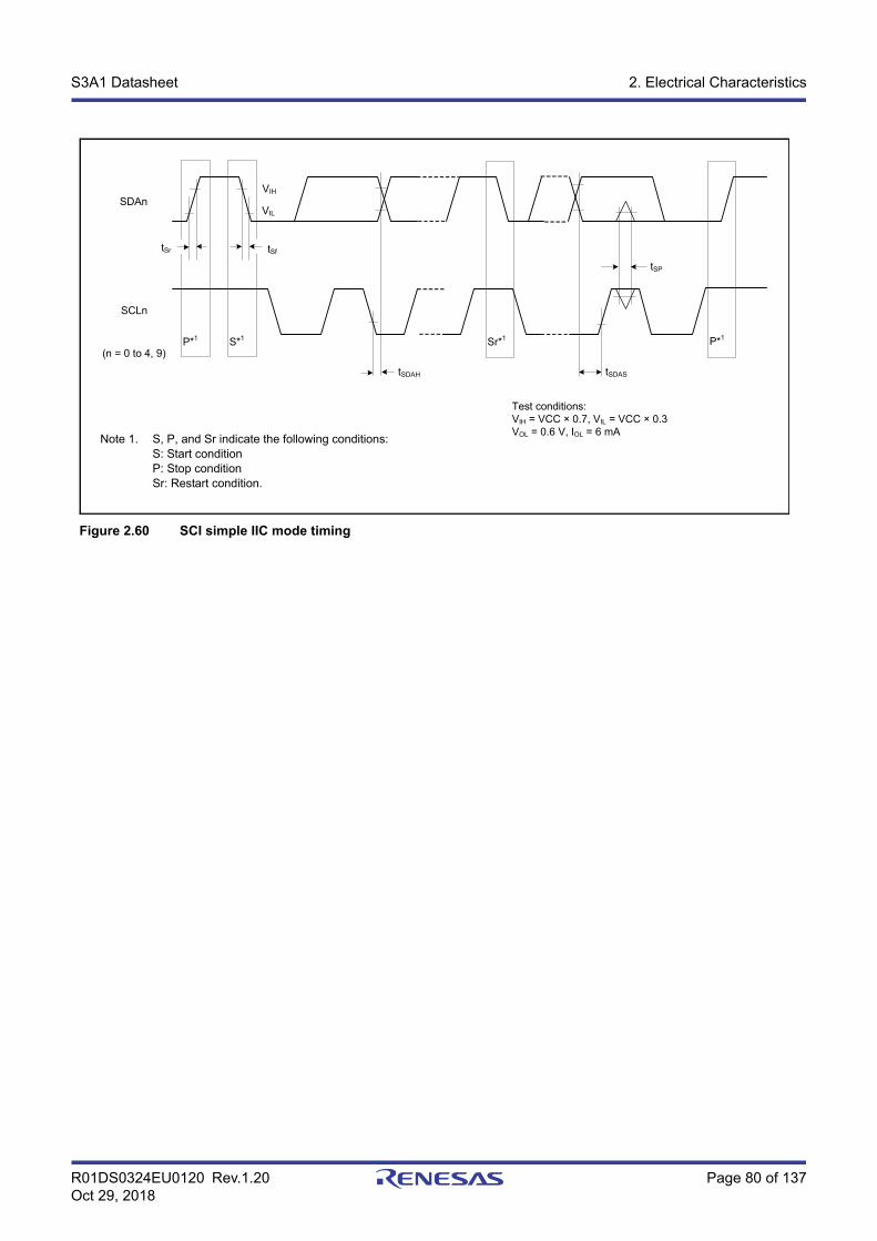
R01DS0324EU0120 Rev.1.20 Page 80 of 137Oct 29, 2018
S3A1 Datasheet 2. Electrical Characteristics
Figure 2.60 SCI simple IIC mode timing
SDAn
SCLn
VIH
VIL
P*1 S*1
tSftSr
tSDAH tSDAS
tSP
P*1
Test conditions:VIH = VCC × 0.7, VIL = VCC × 0.3VOL = 0.6 V, IOL = 6 mA
Sr*1
(n = 0 to 4, 9)
Note 1. S, P, and Sr indicate the following conditions:S: Start conditionP: Stop conditionSr: Restart condition.
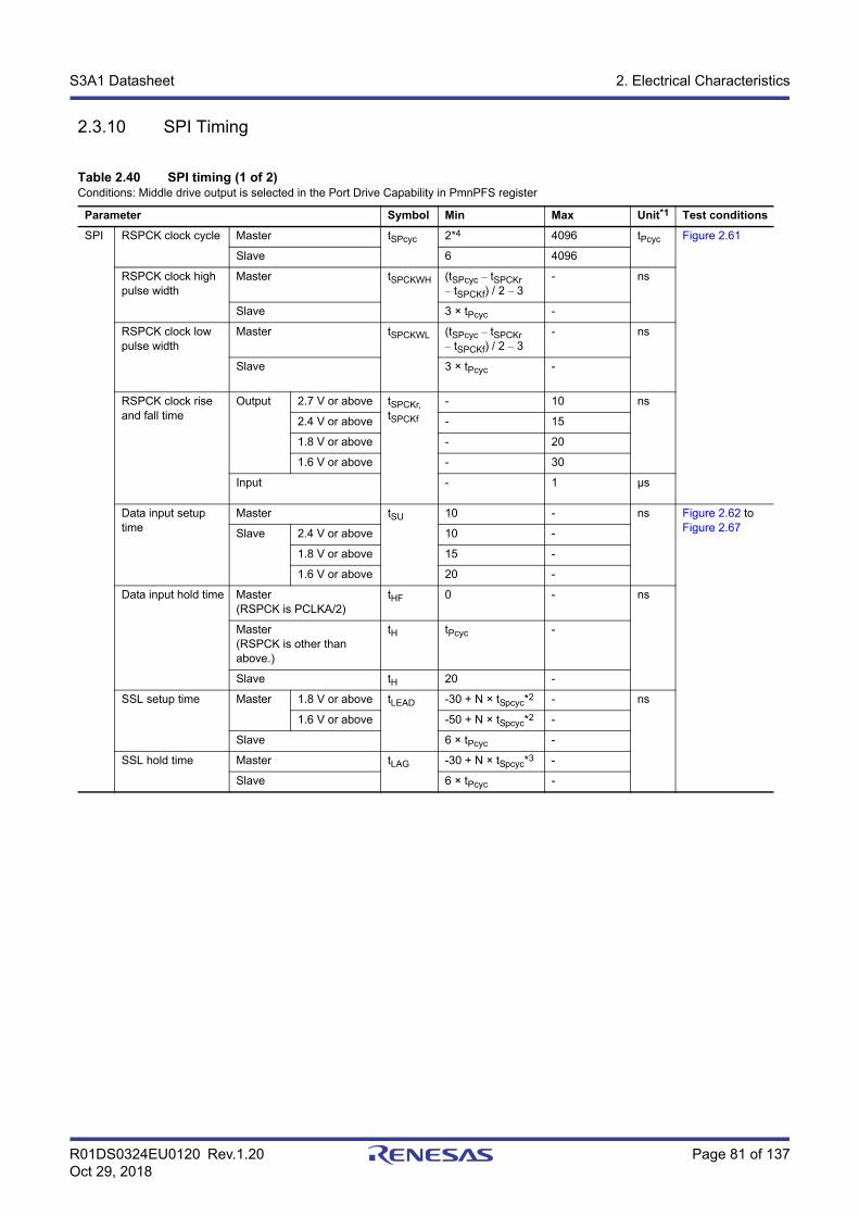
R01DS0324EU0120 Rev.1.20 Page 81 of 137Oct 29, 2018
S3A1 Datasheet 2. Electrical Characteristics
2.3.10 SPI Timing
Table 2.40 SPI timing (1 of 2)Conditions: Middle drive output is selected in the Port Drive Capability in PmnPFS register
Parameter Symbol Min Max Unit*1 Test conditions
SPI RSPCK clock cycle Master tSPcyc 2*4 4096 tPcyc Figure 2.61
Slave 6 4096
RSPCK clock high pulse width
Master tSPCKWH (tSPcyc – tSPCKr– tSPCKf) / 2 – 3
- ns
Slave 3 × tPcyc -
RSPCK clock low pulse width
Master tSPCKWL (tSPcyc – tSPCKr– tSPCKf) / 2 – 3
- ns
Slave 3 × tPcyc -
RSPCK clock rise and fall time
Output 2.7 V or above tSPCKr, tSPCKf
- 10 ns
2.4 V or above - 15
1.8 V or above - 20
1.6 V or above - 30
Input - 1 µs
Data input setup time
Master tSU 10 - ns Figure 2.62 to Figure 2.67Slave 2.4 V or above 10 -
1.8 V or above 15 -
1.6 V or above 20 -
Data input hold time Master(RSPCK is PCLKA/2)
tHF 0 - ns
Master(RSPCK is other than above.)
tH tPcyc -
Slave tH 20 -
SSL setup time Master 1.8 V or above tLEAD -30 + N × tSpcyc*2 - ns
1.6 V or above -50 + N × tSpcyc*2 -
Slave 6 × tPcyc -
SSL hold time Master tLAG -30 + N × tSpcyc*3 -
Slave 6 × tPcyc -
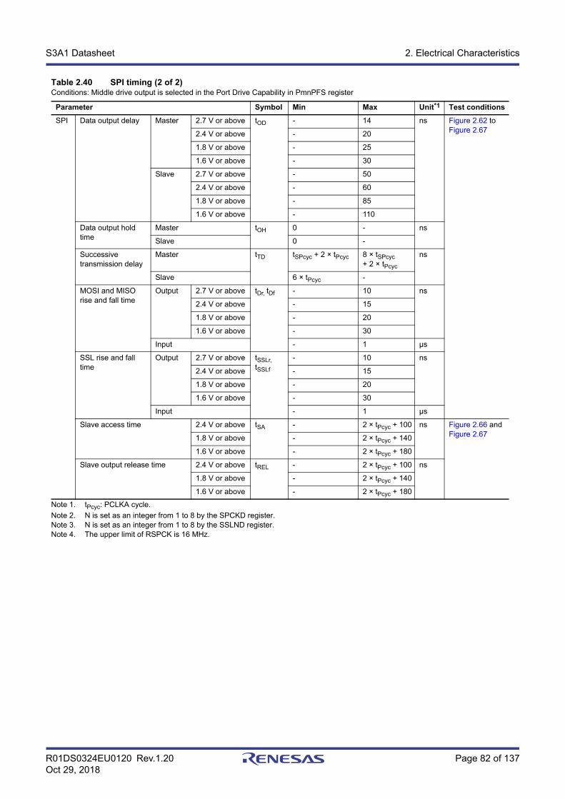
R01DS0324EU0120 Rev.1.20 Page 82 of 137Oct 29, 2018
S3A1 Datasheet 2. Electrical Characteristics
Note 1. tPcyc: PCLKA cycle.
Note 2. N is set as an integer from 1 to 8 by the SPCKD register.Note 3. N is set as an integer from 1 to 8 by the SSLND register.Note 4. The upper limit of RSPCK is 16 MHz.
SPI Data output delay Master 2.7 V or above tOD - 14 ns Figure 2.62 to Figure 2.67 2.4 V or above - 20
1.8 V or above - 25
1.6 V or above - 30
Slave 2.7 V or above - 50
2.4 V or above - 60
1.8 V or above - 85
1.6 V or above - 110
Data output hold time
Master tOH 0 - ns
Slave 0 -
Successive transmission delay
Master tTD tSPcyc + 2 × tPcyc 8 × tSPcyc+ 2 × tPcyc
ns
Slave 6 × tPcyc -
MOSI and MISO rise and fall time
Output 2.7 V or above tDr, tDf - 10 ns
2.4 V or above - 15
1.8 V or above - 20
1.6 V or above - 30
Input - 1 µs
SSL rise and fall time
Output 2.7 V or above tSSLr, tSSLf
- 10 ns
2.4 V or above - 15
1.8 V or above - 20
1.6 V or above - 30
Input - 1 µs
Slave access time 2.4 V or above tSA - 2 × tPcyc + 100 ns Figure 2.66 and Figure 2.671.8 V or above - 2 × tPcyc + 140
1.6 V or above - 2 × tPcyc + 180
Slave output release time 2.4 V or above tREL - 2 × tPcyc + 100 ns
1.8 V or above - 2 × tPcyc + 140
1.6 V or above - 2 × tPcyc + 180
Table 2.40 SPI timing (2 of 2)Conditions: Middle drive output is selected in the Port Drive Capability in PmnPFS register
Parameter Symbol Min Max Unit*1 Test conditions
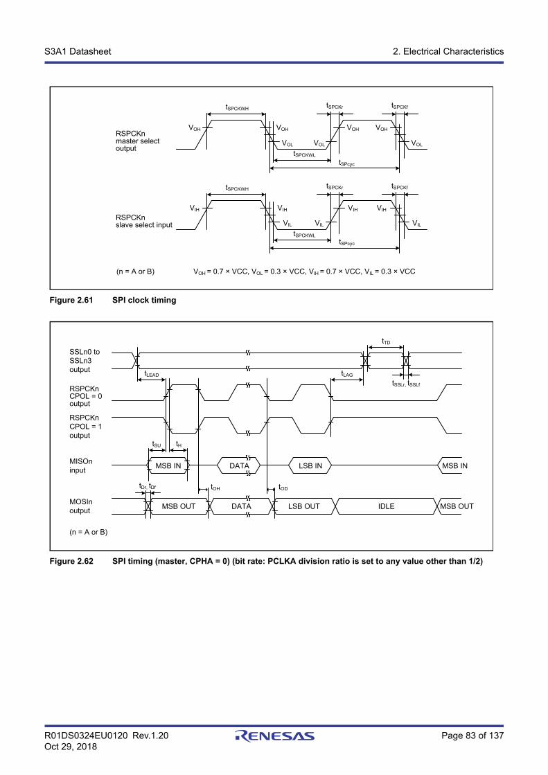
R01DS0324EU0120 Rev.1.20 Page 83 of 137Oct 29, 2018
S3A1 Datasheet 2. Electrical Characteristics
Figure 2.61 SPI clock timing
Figure 2.62 SPI timing (master, CPHA = 0) (bit rate: PCLKA division ratio is set to any value other than 1/2)
RSPCKnmaster select output
RSPCKnslave select input
tSPCKWH
VOH VOH
VOL VOL
VOH VOH
tSPCKWL
tSPCKr tSPCKf
VOL
tSPcyc
tSPCKWH
VIH VIH
VIL VIL
VIH VIH
tSPCKWL
tSPCKr tSPCKf
VIL
tSPcyc
VOH = 0.7 × VCC, VOL = 0.3 × VCC, VIH = 0.7 × VCC, VIL = 0.3 × VCC(n = A or B)
tDr, tDf
tSU tH
tLEAD
tTD
tLAG
tSSLr, tSSLf
tOH tOD
MSB IN DATA LSB IN MSB IN
MSB OUT DATA LSB OUT IDLE MSB OUT
SSLn0 to SSLn3output
RSPCKnCPOL = 0output
RSPCKnCPOL = 1output
MISOninput
MOSInoutput
(n = A or B)
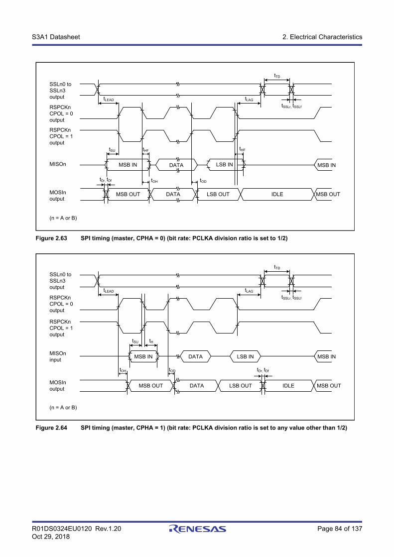
R01DS0324EU0120 Rev.1.20 Page 84 of 137Oct 29, 2018
S3A1 Datasheet 2. Electrical Characteristics
Figure 2.63 SPI timing (master, CPHA = 0) (bit rate: PCLKA division ratio is set to 1/2)
Figure 2.64 SPI timing (master, CPHA = 1) (bit rate: PCLKA division ratio is set to any value other than 1/2)
SSLn0 to SSLn3output
RSPCKnCPOL = 0output
RSPCKnCPOL = 1output
MISOn
MOSInoutput
LSB IN
tDr, tDf
tSU tHF
tLEAD
tTD
tLAG
tSSLr, tSSLf
tOH tOD
MSB IN
MSB OUT DATA LSB OUT IDLE MSB OUT
MSB IN DATA
tHF
(n = A or B)
tSU tH
tLEAD
tTD
tLAG
tSSLr, tSSLf
tOH tOD
MSB IN DATA LSB IN MSB IN
MSB OUT DATA LSB OUT IDLE MSB OUT
SSLn0 to SSLn3output
RSPCKnCPOL = 0output
RSPCKnCPOL = 1output
MISOninput
MOSInoutput
tDr, tDf
(n = A or B)
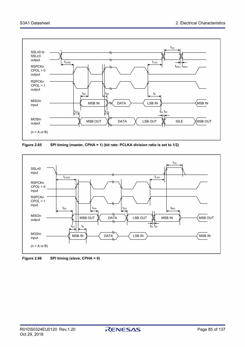
R01DS0324EU0120 Rev.1.20 Page 85 of 137Oct 29, 2018
S3A1 Datasheet 2. Electrical Characteristics
Figure 2.65 SPI timing (master, CPHA = 1) (bit rate: PCLKA division ratio is set to 1/2)
Figure 2.66 SPI timing (slave, CPHA = 0)
tSU tHF
tLEAD
tTD
tLAG
tSSLr, tSSLf
tOH tOD
MSB IN DATA LSB IN MSB IN
MSB OUT DATA LSB OUT IDLE MSB OUT
SSLn0 to SSLn3output
RSPCKnCPOL = 0output
RSPCKnCPOL = 1output
MISOninput
MOSInoutput
tDr, tDf
tH
(n = A or B)
tDr, tDftSU tH
tLEAD
tTD
tLAG
tSA
MSB IN DATA LSB IN MSB IN
MSB OUT DATA LSB OUT MSB IN MSB OUT
tOH tOD tREL
SSLn0input
RSPCKnCPOL = 0input
RSPCKnCPOL = 1input
MISOnoutput
MOSIninput
(n = A or B)
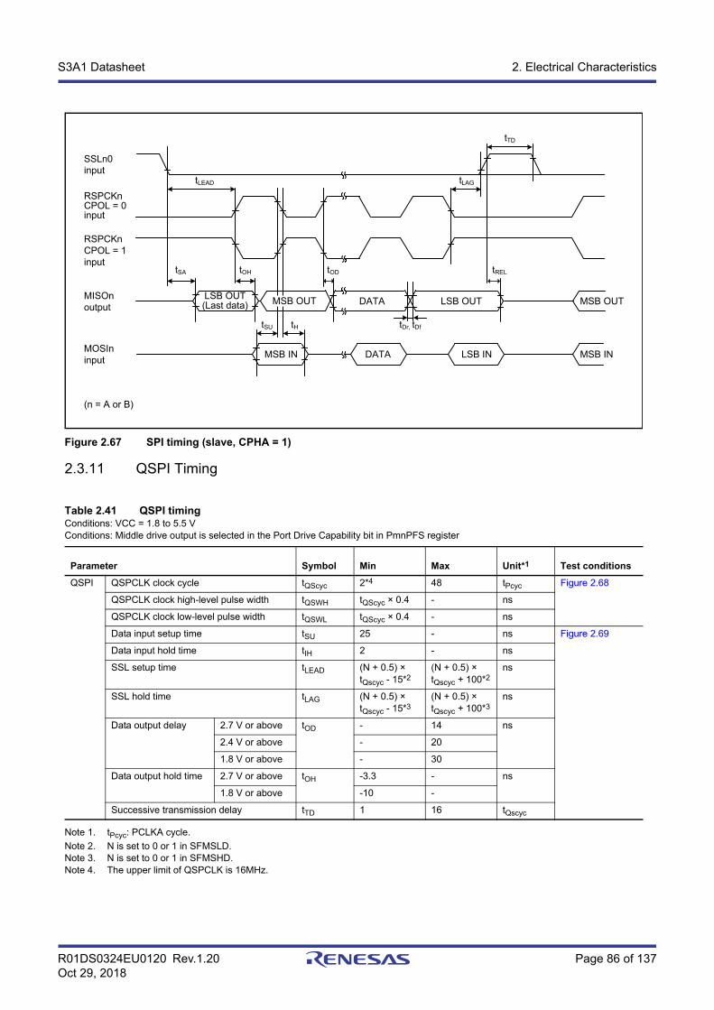
R01DS0324EU0120 Rev.1.20 Page 86 of 137Oct 29, 2018
S3A1 Datasheet 2. Electrical Characteristics
Figure 2.67 SPI timing (slave, CPHA = 1)
2.3.11 QSPI Timing
Note 1. tPcyc: PCLKA cycle.
Note 2. N is set to 0 or 1 in SFMSLD.Note 3. N is set to 0 or 1 in SFMSHD.Note 4. The upper limit of QSPCLK is 16MHz.
Table 2.41 QSPI timingConditions: VCC = 1.8 to 5.5 VConditions: Middle drive output is selected in the Port Drive Capability bit in PmnPFS register
Parameter Symbol Min Max Unit*1 Test conditions
QSPI QSPCLK clock cycle tQScyc 2*4 48 tPcyc Figure 2.68
QSPCLK clock high-level pulse width tQSWH tQScyc × 0.4 - ns
QSPCLK clock low-level pulse width tQSWL tQScyc × 0.4 - ns
Data input setup time tSU 25 - ns Figure 2.69
Data input hold time tIH 2 - ns
SSL setup time tLEAD (N + 0.5) × tQscyc - 15*2
(N + 0.5) × tQscyc + 100*2
ns
SSL hold time tLAG (N + 0.5) × tQscyc - 15*3
(N + 0.5) × tQscyc + 100*3
ns
Data output delay 2.7 V or above tOD - 14 ns
2.4 V or above - 20
1.8 V or above - 30
Data output hold time 2.7 V or above tOH -3.3 - ns
1.8 V or above -10 -
Successive transmission delay tTD 1 16 tQscyc
SSLn0input
RSPCKnCPOL = 0input
RSPCKnCPOL = 1input
MISOnoutput
MOSIninput
tDr, tDf
tSA tOH
tLEAD
tTD
tLAG
tH
LSB OUT(Last data) DATA MSB OUT
MSB IN DATA LSB IN MSB IN
LSB OUT
tSU
tOD tREL
MSB OUT
(n = A or B)
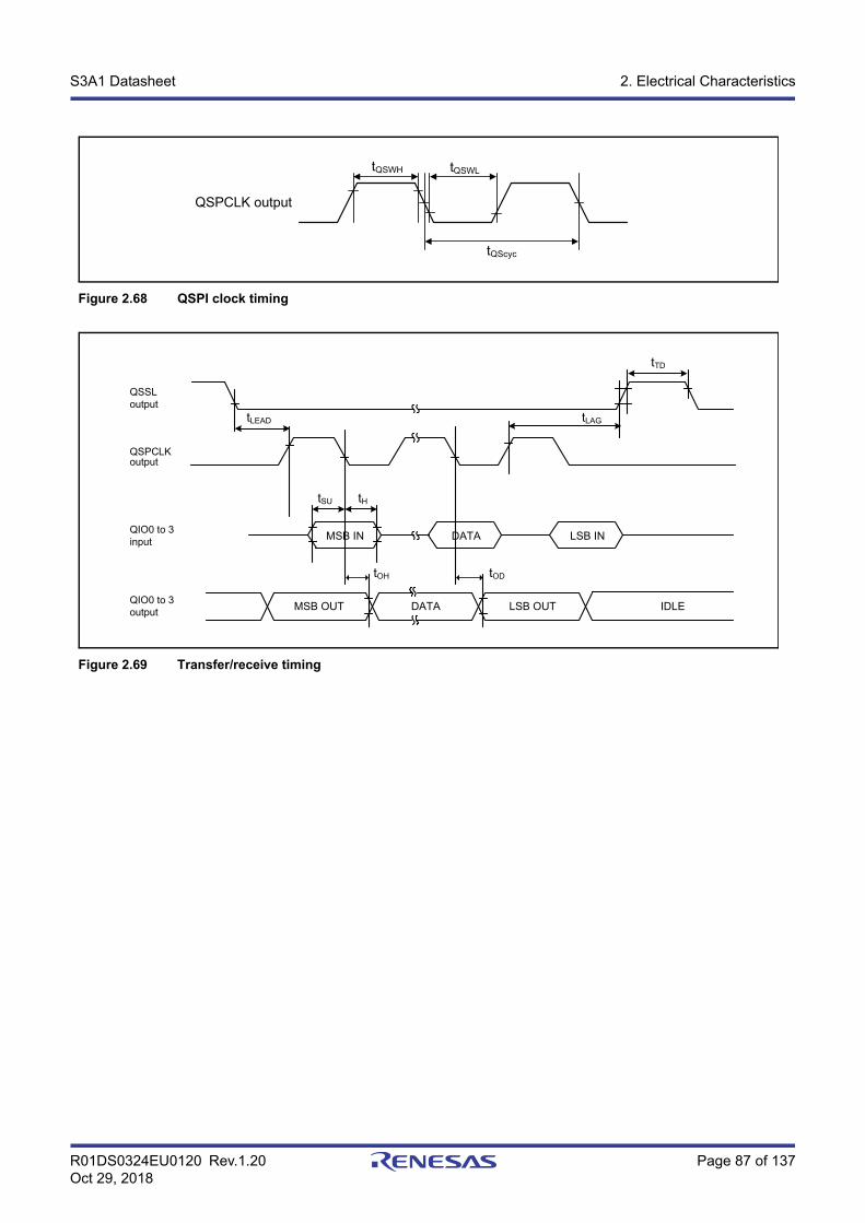
R01DS0324EU0120 Rev.1.20 Page 87 of 137Oct 29, 2018
S3A1 Datasheet 2. Electrical Characteristics
Figure 2.68 QSPI clock timing
Figure 2.69 Transfer/receive timing
tQScyc
QSPCLK output
tQSWH tQSWL
tSU tH
tLEAD
tTD
tLAG
tOH tOD
MSB IN DATA LSB IN
MSB OUT DATA LSB OUT IDLE
QSSLoutput
QSPCLKoutput
QIO0 to 3input
QIO0 to 3output
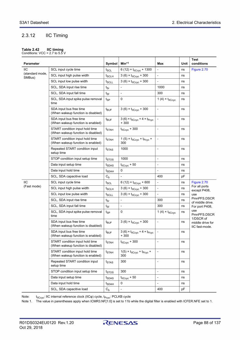
R01DS0324EU0120 Rev.1.20 Page 88 of 137Oct 29, 2018
S3A1 Datasheet 2. Electrical Characteristics
2.3.12 IIC Timing
Note: tIICcyc: IIC internal reference clock (IICφ) cycle, tPcyc: PCLKB cycle
Note 1. The value in parentheses apply when ICMR3.NF[1:0] is set to 11b while the digital filter is enabled with ICFER.NFE set to 1.
Table 2.42 IIC timingConditions: VCC = 2.7 to 5.5 V
Parameter Symbol Min*1 Max UnitTest conditions
IIC(standard mode, SMBus)
SCL input cycle time tSCL 6 (12) × tIICcyc + 1300 - ns Figure 2.70
SCL input high pulse width tSCLH 3 (6) × tIICcyc + 300 - ns
SCL input low pulse width tSCLL 3 (6) × tIICcyc + 300 - ns
SCL, SDA input rise time tSr - 1000 ns
SCL, SDA input fall time tSf - 300 ns
SCL, SDA input spike pulse removal time
tSP 0 1 (4) × tIICcyc ns
SDA input bus free time(When wakeup function is disabled)
tBUF 3 (6) × tIICcyc + 300 - ns
SDA input bus free time(When wakeup function is enabled)
tBUF 3 (6) × tIICcyc + 4 × tPcyc + 300
- ns
START condition input hold time(When wakeup function is disabled)
tSTAH tIICcyc + 300 - ns
START condition input hold time(When wakeup function is enabled)
tSTAH 1 (5) × tIICcyc + tPcyc + 300
- ns
Repeated START condition input setup time
tSTAS 1000 - ns
STOP condition input setup time tSTOS 1000 - ns
Data input setup time tSDAS tIICcyc + 50 - ns
Data input hold time tSDAH 0 - ns
SCL, SDA capacitive load Cb - 400 pF
IIC(Fast mode)
SCL input cycle time tSCL 6 (12) × tIICcyc + 600 - ns Figure 2.70For all ports except P408, use PmnPFS.DSCR of middle drive.For port P408, use PmnPFS.DSCR1/DSCR of middle drive for IIC fast-mode.
SCL input high pulse width tSCLH 3 (6) × tIICcyc + 300 - ns
SCL input low pulse width tSCLL 3 (6) × tIICcyc + 300 - ns
SCL, SDA input rise time tSr - 300 ns
SCL, SDA input fall time tSf - 300 ns
SCL, SDA input spike pulse removal time
tSP 0 1 (4) × tIICcyc ns
SDA input bus free time (When wakeup function is disabled)
tBUF 3 (6) × tIICcyc + 300 - ns
SDA input bus free time(When wakeup function is enabled)
tBUF 3 (6) × tIICcyc + 4 × tPcyc + 300
- ns
START condition input hold time(When wakeup function is disabled)
tSTAH tIICcyc + 300 - ns
START condition input hold time(When wakeup function is enabled)
tSTAH 1(5) × tIICcyc + tPcyc + 300
- ns
Repeated START condition input setup time
tSTAS 300 - ns
STOP condition input setup time tSTOS 300 - ns
Data input setup time tSDAS tIICcyc + 50 - ns
Data input hold time tSDAH 0 - ns
SCL, SDA capacitive load Cb - 400 pF
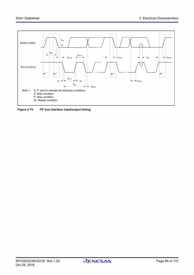
R01DS0324EU0120 Rev.1.20 Page 89 of 137Oct 29, 2018
S3A1 Datasheet 2. Electrical Characteristics
Figure 2.70 I2C bus interface input/output timing
SDA0 to SDA2
SCL0 to SCL2
VIH
VIL
tSTAH
tSCLH
tSCLL
P*1 S*1
tSf tSr
tSCLtSDAH
tSDAS
tSTAS tSP tSTOS
P*1
tBUF
Sr*1
Note 1. S, P, and Sr indicate the following conditions.S: Start conditionP: Stop conditionSr: Restart condition
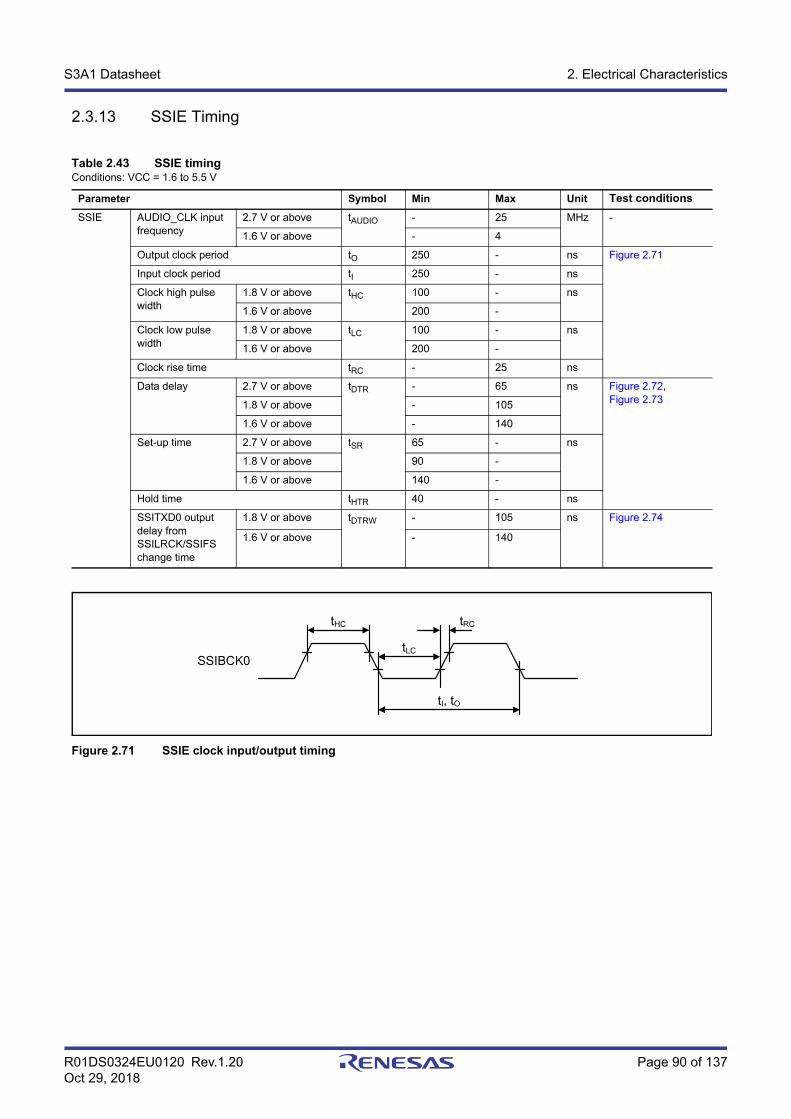
R01DS0324EU0120 Rev.1.20 Page 90 of 137Oct 29, 2018
S3A1 Datasheet 2. Electrical Characteristics
2.3.13 SSIE Timing
Figure 2.71 SSIE clock input/output timing
Table 2.43 SSIE timingConditions: VCC = 1.6 to 5.5 V
Parameter Symbol Min Max Unit Test conditions
SSIE AUDIO_CLK input frequency
2.7 V or above tAUDIO - 25 MHz -
1.6 V or above - 4
Output clock period tO 250 - ns Figure 2.71
Input clock period tI 250 - ns
Clock high pulse width
1.8 V or above tHC 100 - ns
1.6 V or above 200 -
Clock low pulse width
1.8 V or above tLC 100 - ns
1.6 V or above 200 -
Clock rise time tRC - 25 ns
Data delay 2.7 V or above tDTR - 65 ns Figure 2.72,Figure 2.731.8 V or above - 105
1.6 V or above - 140
Set-up time 2.7 V or above tSR 65 - ns
1.8 V or above 90 -
1.6 V or above 140 -
Hold time tHTR 40 - ns
SSITXD0 output delay from SSILRCK/SSIFS change time
1.8 V or above tDTRW - 105 ns Figure 2.74
1.6 V or above - 140
SSIBCK0
tHC
tLC
tRC
tI, tO
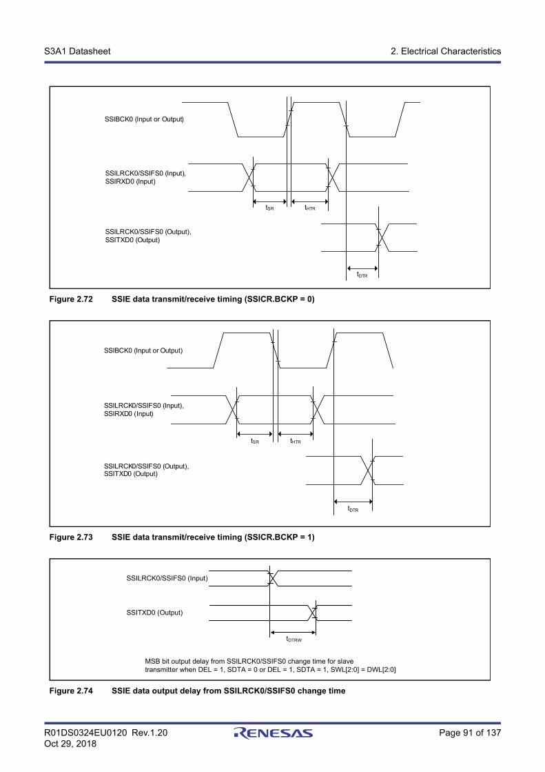
R01DS0324EU0120 Rev.1.20 Page 91 of 137Oct 29, 2018
S3A1 Datasheet 2. Electrical Characteristics
Figure 2.72 SSIE data transmit/receive timing (SSICR.BCKP = 0)
Figure 2.73 SSIE data transmit/receive timing (SSICR.BCKP = 1)
Figure 2.74 SSIE data output delay from SSILRCK0/SSIFS0 change time
tSR tHTR
tDTR
SSIBCK0 (Input or Output)
SSILRCK0/SSIFS0 (Input), SSIRXD0 (Input)
SSILRCK0/SSIFS0 (Output), SSITXD0 (Output)
tSR tHTR
tDTR
SSIBCK0 (Input or Output)
SSILRCK0/SSIFS0 (Input), SSIRXD0 (Input)
SSILRCK0/SSIFS0 (Output), SSITXD0 (Output)
tDTRW
SSILRCK0/SSIFS0 (Input)
SSITXD0 (Output)
MSB bit output delay from SSILRCK0/SSIFS0 change time for slave transmitter when DEL = 1, SDTA = 0 or DEL = 1, SDTA = 1, SWL[2:0] = DWL[2:0]
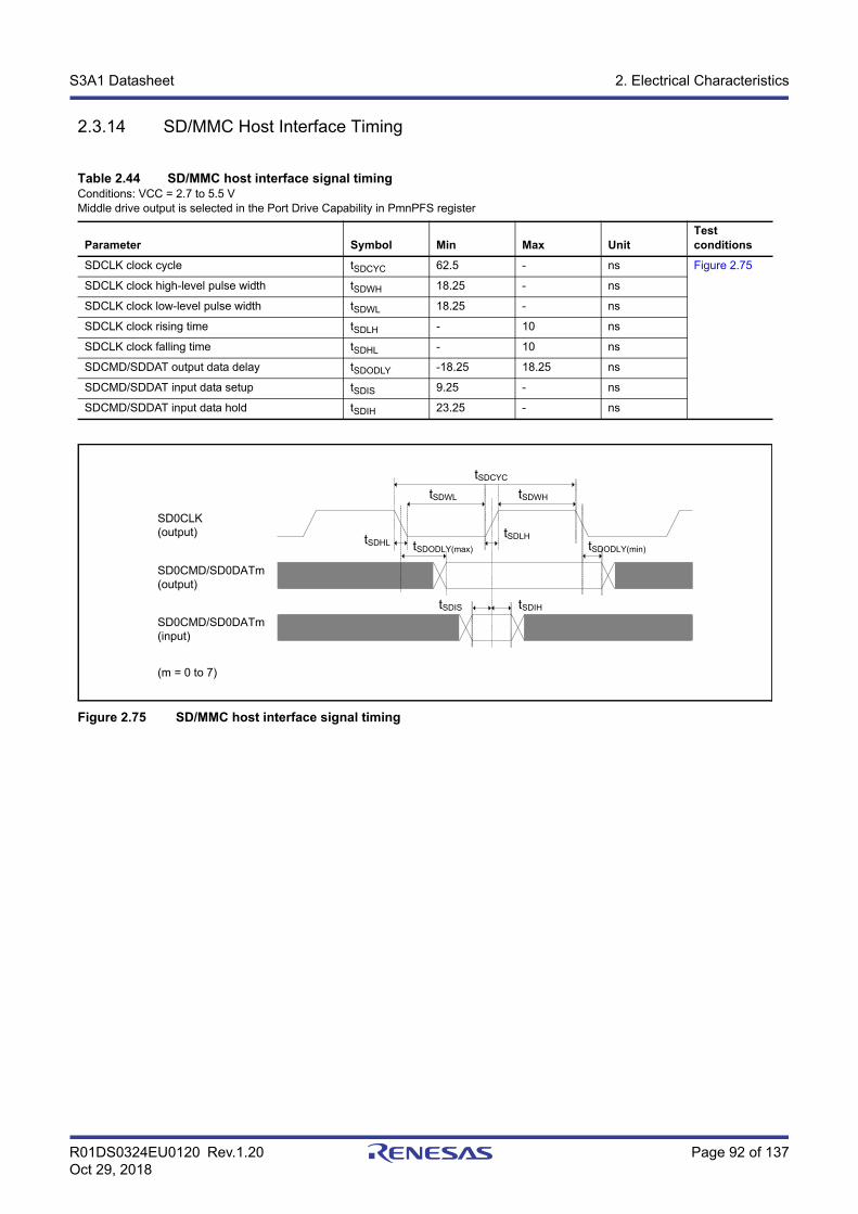
R01DS0324EU0120 Rev.1.20 Page 92 of 137Oct 29, 2018
S3A1 Datasheet 2. Electrical Characteristics
2.3.14 SD/MMC Host Interface Timing
Figure 2.75 SD/MMC host interface signal timing
Table 2.44 SD/MMC host interface signal timingConditions: VCC = 2.7 to 5.5 VMiddle drive output is selected in the Port Drive Capability in PmnPFS register
Parameter Symbol Min Max UnitTest conditions
SDCLK clock cycle tSDCYC 62.5 - ns Figure 2.75
SDCLK clock high-level pulse width tSDWH 18.25 - ns
SDCLK clock low-level pulse width tSDWL 18.25 - ns
SDCLK clock rising time tSDLH - 10 ns
SDCLK clock falling time tSDHL - 10 ns
SDCMD/SDDAT output data delay tSDODLY -18.25 18.25 ns
SDCMD/SDDAT input data setup tSDIS 9.25 - ns
SDCMD/SDDAT input data hold tSDIH 23.25 - ns
SD0CLK(output)
SD0CMD/SD0DATm(input)
SD0CMD/SD0DATm(output)
tSDODLY(max)
tSDIS tSDIH
tSDLHtSDHL
tSDCYC
tSDWHtSDWL
tSDODLY(min)
(m = 0 to 7)
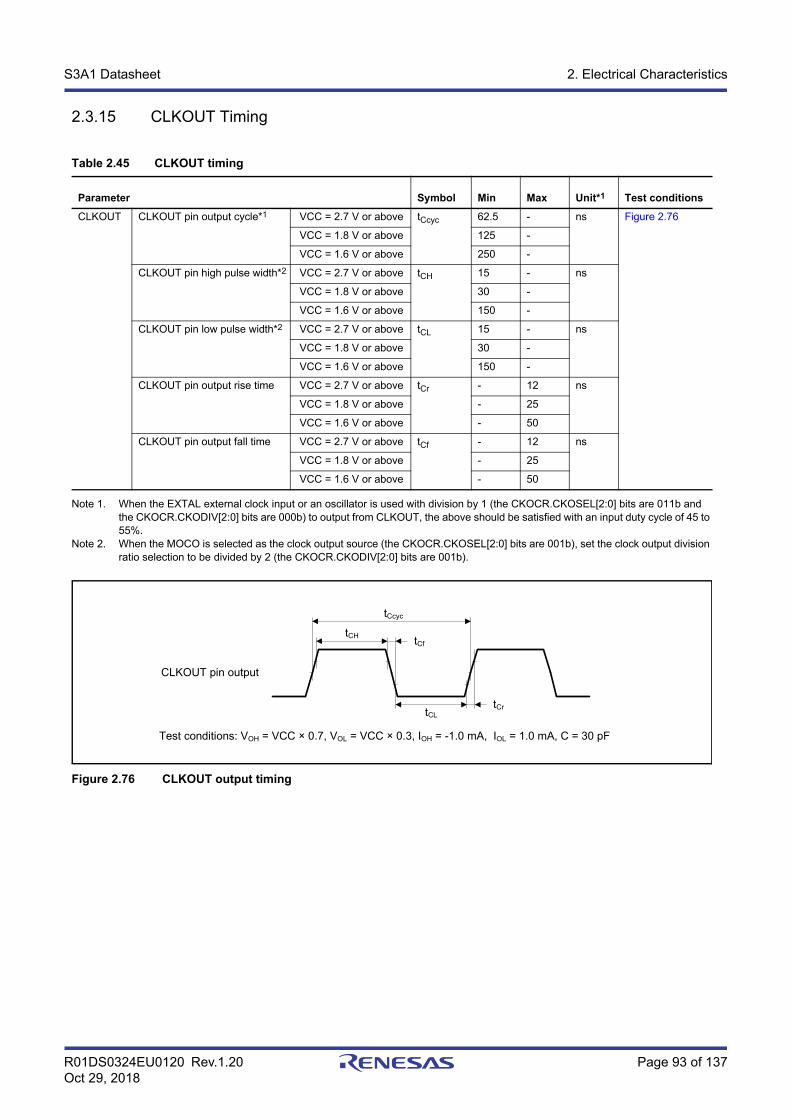
R01DS0324EU0120 Rev.1.20 Page 93 of 137Oct 29, 2018
S3A1 Datasheet 2. Electrical Characteristics
2.3.15 CLKOUT Timing
Note 1. When the EXTAL external clock input or an oscillator is used with division by 1 (the CKOCR.CKOSEL[2:0] bits are 011b and the CKOCR.CKODIV[2:0] bits are 000b) to output from CLKOUT, the above should be satisfied with an input duty cycle of 45 to 55%.
Note 2. When the MOCO is selected as the clock output source (the CKOCR.CKOSEL[2:0] bits are 001b), set the clock output division ratio selection to be divided by 2 (the CKOCR.CKODIV[2:0] bits are 001b).
Figure 2.76 CLKOUT output timing
Table 2.45 CLKOUT timing
Parameter Symbol Min Max Unit*1 Test conditions
CLKOUT CLKOUT pin output cycle*1 VCC = 2.7 V or above tCcyc 62.5 - ns Figure 2.76
VCC = 1.8 V or above 125 -
VCC = 1.6 V or above 250 -
CLKOUT pin high pulse width*2 VCC = 2.7 V or above tCH 15 - ns
VCC = 1.8 V or above 30 -
VCC = 1.6 V or above 150 -
CLKOUT pin low pulse width*2 VCC = 2.7 V or above tCL 15 - ns
VCC = 1.8 V or above 30 -
VCC = 1.6 V or above 150 -
CLKOUT pin output rise time VCC = 2.7 V or above tCr - 12 ns
VCC = 1.8 V or above - 25
VCC = 1.6 V or above - 50
CLKOUT pin output fall time VCC = 2.7 V or above tCf - 12 ns
VCC = 1.8 V or above - 25
VCC = 1.6 V or above - 50
tCftCH
tCcyc
tCrtCL
CLKOUT pin output
Test conditions: VOH = VCC × 0.7, VOL = VCC × 0.3, IOH = -1.0 mA, IOL = 1.0 mA, C = 30 pF
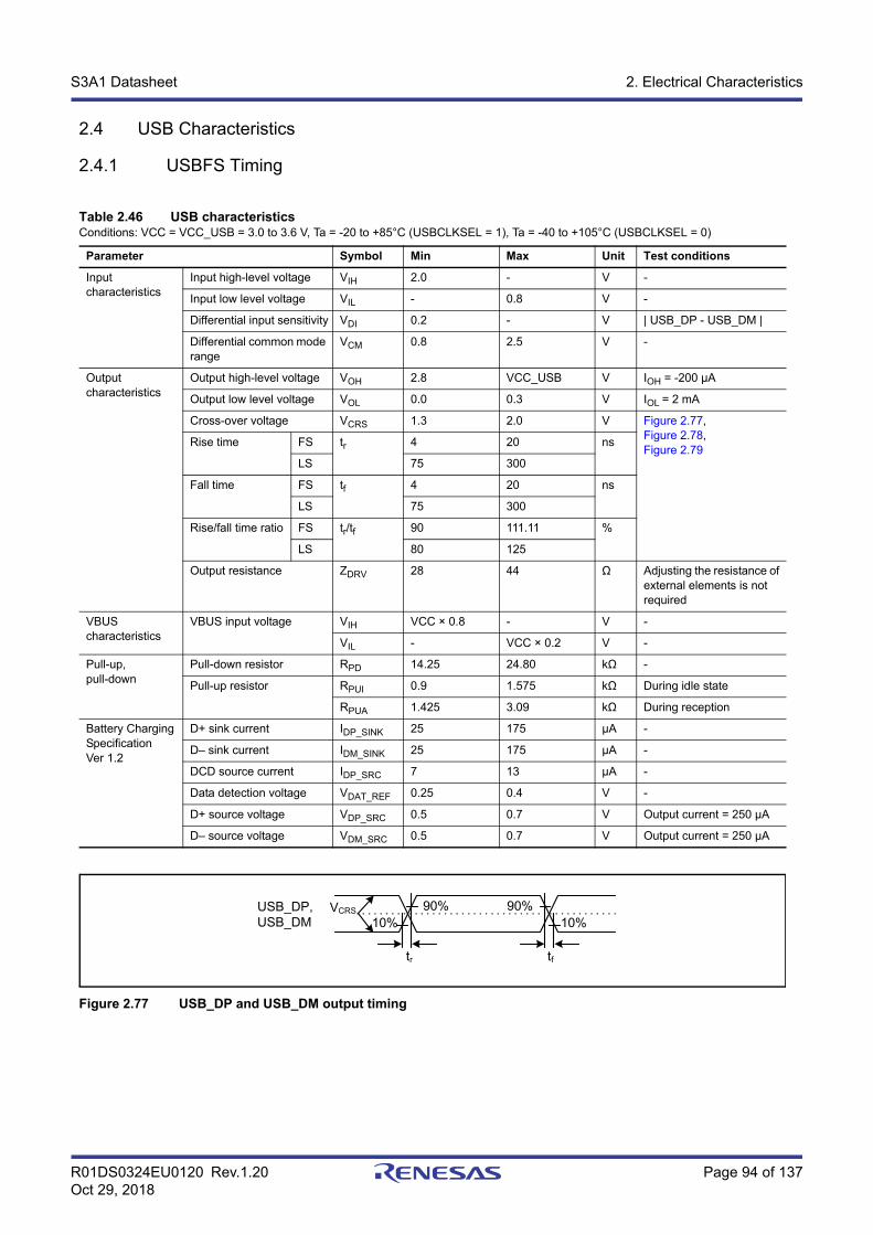
R01DS0324EU0120 Rev.1.20 Page 94 of 137Oct 29, 2018
S3A1 Datasheet 2. Electrical Characteristics
2.4 USB Characteristics
2.4.1 USBFS Timing
Figure 2.77 USB_DP and USB_DM output timing
Table 2.46 USB characteristicsConditions: VCC = VCC_USB = 3.0 to 3.6 V, Ta = -20 to +85°C (USBCLKSEL = 1), Ta = -40 to +105°C (USBCLKSEL = 0)
Parameter Symbol Min Max Unit Test conditions
Input characteristics
Input high-level voltage VIH 2.0 - V -
Input low level voltage VIL - 0.8 V -
Differential input sensitivity VDI 0.2 - V | USB_DP - USB_DM |
Differential common mode range
VCM 0.8 2.5 V -
Output characteristics
Output high-level voltage VOH 2.8 VCC_USB V IOH = -200 μA
Output low level voltage VOL 0.0 0.3 V IOL = 2 mA
Cross-over voltage VCRS 1.3 2.0 V Figure 2.77,Figure 2.78,Figure 2.79
Rise time FS tr 4 20 ns
LS 75 300
Fall time FS tf 4 20 ns
LS 75 300
Rise/fall time ratio FS tr/tf 90 111.11 %
LS 80 125
Output resistance ZDRV 28 44 Ω Adjusting the resistance of external elements is not required
VBUS characteristics
VBUS input voltage VIH VCC × 0.8 - V -
VIL - VCC × 0.2 V -
Pull-up, pull-down
Pull-down resistor RPD 14.25 24.80 kΩ -
Pull-up resistor RPUI 0.9 1.575 kΩ During idle state
RPUA 1.425 3.09 kΩ During reception
Battery Charging Specification Ver 1.2
D+ sink current IDP_SINK 25 175 μA -
D– sink current IDM_SINK 25 175 μA -
DCD source current IDP_SRC 7 13 μA -
Data detection voltage VDAT_REF 0.25 0.4 V -
D+ source voltage VDP_SRC 0.5 0.7 V Output current = 250 μA
D– source voltage VDM_SRC 0.5 0.7 V Output current = 250 μA
USB_DP,USB_DM
tftr
90%10%10%
90%VCRS
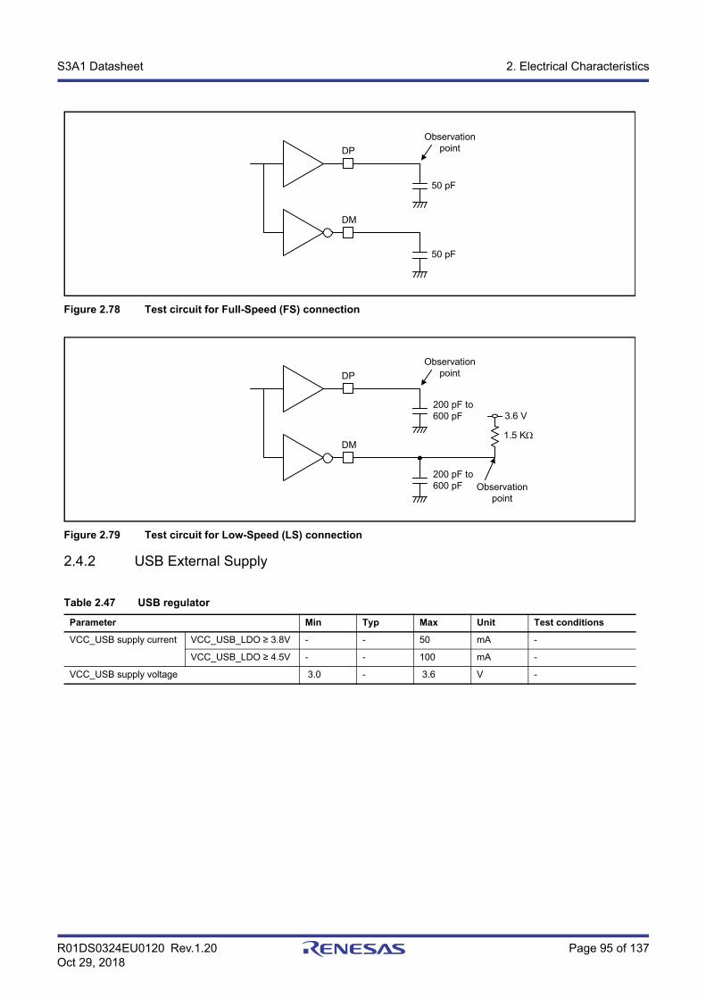
R01DS0324EU0120 Rev.1.20 Page 95 of 137Oct 29, 2018
S3A1 Datasheet 2. Electrical Characteristics
Figure 2.78 Test circuit for Full-Speed (FS) connection
Figure 2.79 Test circuit for Low-Speed (LS) connection
2.4.2 USB External Supply
Table 2.47 USB regulator
Parameter Min Typ Max Unit Test conditions
VCC_USB supply current VCC_USB_LDO ≥ 3.8V - - 50 mA -
VCC_USB_LDO ≥ 4.5V - - 100 mA -
VCC_USB supply voltage 3.0 - 3.6 V -
Observation point
50 pF
DP
DM
50 pF
Observation point
200 pF to 600 pF
DP
DM
200 pF to 600 pF
1.5 K
3.6 V
Observation point
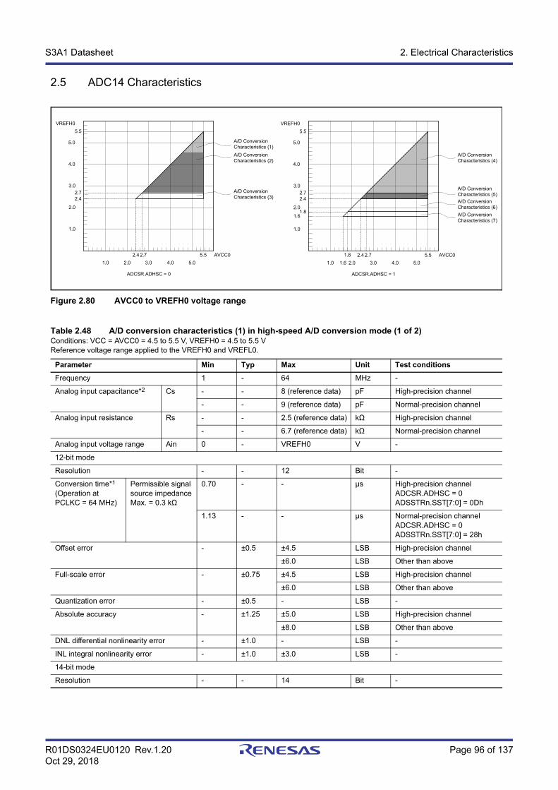
R01DS0324EU0120 Rev.1.20 Page 96 of 137Oct 29, 2018
S3A1 Datasheet 2. Electrical Characteristics
2.5 ADC14 Characteristics
Figure 2.80 AVCC0 to VREFH0 voltage range
Table 2.48 A/D conversion characteristics (1) in high-speed A/D conversion mode (1 of 2)Conditions: VCC = AVCC0 = 4.5 to 5.5 V, VREFH0 = 4.5 to 5.5 VReference voltage range applied to the VREFH0 and VREFL0.
Parameter Min Typ Max Unit Test conditions
Frequency 1 - 64 MHz -
Analog input capacitance*2 Cs - - 8 (reference data) pF High-precision channel
- - 9 (reference data) pF Normal-precision channel
Analog input resistance Rs - - 2.5 (reference data) kΩ High-precision channel
- - 6.7 (reference data) kΩ Normal-precision channel
Analog input voltage range Ain 0 - VREFH0 V -
12-bit mode
Resolution - - 12 Bit -
Conversion time*1
(Operation at PCLKC = 64 MHz)
Permissible signal source impedance Max. = 0.3 kΩ
0.70 - - μs High-precision channelADCSR.ADHSC = 0ADSSTRn.SST[7:0] = 0Dh
1.13 - - μs Normal-precision channelADCSR.ADHSC = 0ADSSTRn.SST[7:0] = 28h
Offset error - ±0.5 ±4.5 LSB High-precision channel
±6.0 LSB Other than above
Full-scale error - ±0.75 ±4.5 LSB High-precision channel
±6.0 LSB Other than above
Quantization error - ±0.5 - LSB -
Absolute accuracy - ±1.25 ±5.0 LSB High-precision channel
±8.0 LSB Other than above
DNL differential nonlinearity error - ±1.0 - LSB -
INL integral nonlinearity error - ±1.0 ±3.0 LSB -
14-bit mode
Resolution - - 14 Bit -
VREFH0
5.0
4.0
3.0
2.0
1.0
1.0 2.0 3.0 4.0 5.0
A/D Conversion Characteristics (2)
ADCSR.ADHSC = 0
5.5
2.72.4
2.4 2.7 5.5 AVCC0
VREFH0
5.0
4.0
3.0
2.0
1.0
1.0 2.0 3.0 4.0 5.0
ADCSR.ADHSC = 1
5.5
2.72.4
2.4 2.7 5.5 AVCC0
1.8
1.8
A/D Conversion Characteristics (1)
A/D Conversion Characteristics (3)
A/D Conversion Characteristics (4)
A/D Conversion Characteristics (5)
A/D Conversion Characteristics (6)
A/D Conversion Characteristics (7)
1.6
1.6
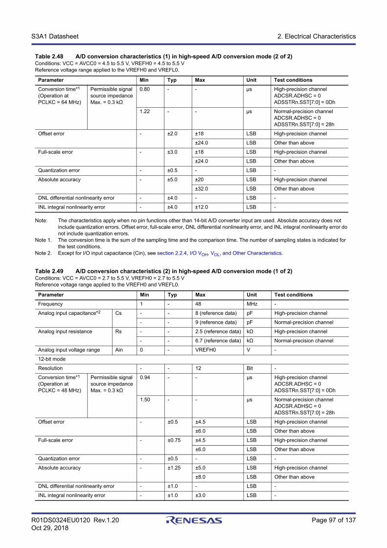
R01DS0324EU0120 Rev.1.20 Page 97 of 137Oct 29, 2018
S3A1 Datasheet 2. Electrical Characteristics
Note: The characteristics apply when no pin functions other than 14-bit A/D converter input are used. Absolute accuracy does not include quantization errors. Offset error, full-scale error, DNL differential nonlinearity error, and INL integral nonlinearity error do not include quantization errors.
Note 1. The conversion time is the sum of the sampling time and the comparison time. The number of sampling states is indicated for the test conditions.
Note 2. Except for I/O input capacitance (Cin), see section 2.2.4, I/O VOH, VOL, and Other Characteristics.
Conversion time*1
(Operation at PCLKC = 64 MHz)
Permissible signal source impedance Max. = 0.3 kΩ
0.80 - - μs High-precision channelADCSR.ADHSC = 0ADSSTRn.SST[7:0] = 0Dh
1.22 - - μs Normal-precision channelADCSR.ADHSC = 0ADSSTRn.SST[7:0] = 28h
Offset error - ±2.0 ±18 LSB High-precision channel
±24.0 LSB Other than above
Full-scale error - ±3.0 ±18 LSB High-precision channel
±24.0 LSB Other than above
Quantization error - ±0.5 - LSB -
Absolute accuracy - ±5.0 ±20 LSB High-precision channel
±32.0 LSB Other than above
DNL differential nonlinearity error - ±4.0 - LSB -
INL integral nonlinearity error - ±4.0 ±12.0 LSB -
Table 2.49 A/D conversion characteristics (2) in high-speed A/D conversion mode (1 of 2)Conditions: VCC = AVCC0 = 2.7 to 5.5 V, VREFH0 = 2.7 to 5.5 VReference voltage range applied to the VREFH0 and VREFL0.
Parameter Min Typ Max Unit Test conditions
Frequency 1 - 48 MHz -
Analog input capacitance*2 Cs - - 8 (reference data) pF High-precision channel
- - 9 (reference data) pF Normal-precision channel
Analog input resistance Rs - - 2.5 (reference data) kΩ High-precision channel
- - 6.7 (reference data) kΩ Normal-precision channel
Analog input voltage range Ain 0 - VREFH0 V -
12-bit mode
Resolution - - 12 Bit -
Conversion time*1
(Operation at PCLKC = 48 MHz)
Permissible signal source impedance Max. = 0.3 kΩ
0.94 - - μs High-precision channelADCSR.ADHSC = 0ADSSTRn.SST[7:0] = 0Dh
1.50 - - μs Normal-precision channelADCSR.ADHSC = 0ADSSTRn.SST[7:0] = 28h
Offset error - ±0.5 ±4.5 LSB High-precision channel
±6.0 LSB Other than above
Full-scale error - ±0.75 ±4.5 LSB High-precision channel
±6.0 LSB Other than above
Quantization error - ±0.5 - LSB -
Absolute accuracy - ±1.25 ±5.0 LSB High-precision channel
±8.0 LSB Other than above
DNL differential nonlinearity error - ±1.0 - LSB -
INL integral nonlinearity error - ±1.0 ±3.0 LSB -
Table 2.48 A/D conversion characteristics (1) in high-speed A/D conversion mode (2 of 2)Conditions: VCC = AVCC0 = 4.5 to 5.5 V, VREFH0 = 4.5 to 5.5 VReference voltage range applied to the VREFH0 and VREFL0.
Parameter Min Typ Max Unit Test conditions
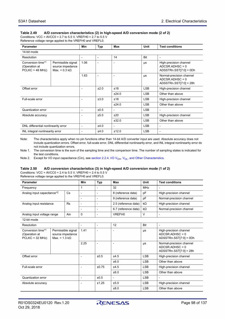
R01DS0324EU0120 Rev.1.20 Page 98 of 137Oct 29, 2018
S3A1 Datasheet 2. Electrical Characteristics
Note: The characteristics apply when no pin functions other than 14-bit A/D converter input are used. Absolute accuracy does not include quantization errors. Offset error, full-scale error, DNL differential nonlinearity error, and INL integral nonlinearity error do not include quantization errors.
Note 1. The conversion time is the sum of the sampling time and the comparison time. The number of sampling states is indicated for the test conditions.
Note 2. Except for I/O input capacitance (Cin), see section 2.2.4, I/O VOH, VOL, and Other Characteristics.
14-bit mode
Resolution - - 14 Bit -
Conversion time*1
(Operation at PCLKC = 48 MHz)
Permissible signal source impedance Max. = 0.3 kΩ
1.06 - - μs High-precision channelADCSR.ADHSC = 0ADSSTRn.SST[7:0] = 0Dh
1.63 - - μs Normal-precision channelADCSR.ADHSC = 0ADSSTRn.SST[7:0] = 28h
Offset error - ±2.0 ±18 LSB High-precision channel
±24.0 LSB Other than above
Full-scale error - ±3.0 ±18 LSB High-precision channel
±24.0 LSB Other than above
Quantization error - ±0.5 - LSB -
Absolute accuracy - ±5.0 ±20 LSB High-precision channel
±32.0 LSB Other than above
DNL differential nonlinearity error - ±4.0 - LSB -
INL integral nonlinearity error - ±4.0 ±12.0 LSB -
Table 2.50 A/D conversion characteristics (3) in high-speed A/D conversion mode (1 of 2)Conditions: VCC = AVCC0 = 2.4 to 5.5 V, VREFH0 = 2.4 to 5.5 VReference voltage range applied to the VREFH0 and VREFL0.
Parameter Min Typ Max Unit Test conditions
Frequency 1 - 32 MHz -
Analog input capacitance*2 Cs - - 8 (reference data) pF High-precision channel
- - 9 (reference data) pF Normal-precision channel
Analog input resistance Rs - - 2.5 (reference data) kΩ High-precision channel
- - 6.7 (reference data) kΩ Normal-precision channel
Analog input voltage range Ain 0 - VREFH0 V -
12-bit mode
Resolution - - 12 Bit -
Conversion time*1
(Operation at PCLKC = 32 MHz)
Permissible signal source impedance Max. = 1.3 kΩ
1.41 - - μs High-precision channelADCSR.ADHSC = 0ADSSTRn.SST[7:0] = 0Dh
2.25 - - μs Normal-precision channelADCSR.ADHSC = 0ADSSTRn.SST[7:0] = 28h
Offset error - ±0.5 ±4.5 LSB High-precision channel
±6.0 LSB Other than above
Full-scale error - ±0.75 ±4.5 LSB High-precision channel
±6.0 LSB Other than above
Quantization error - ±0.5 - LSB -
Absolute accuracy - ±1.25 ±5.0 LSB High-precision channel
±8.0 LSB Other than above
Table 2.49 A/D conversion characteristics (2) in high-speed A/D conversion mode (2 of 2)Conditions: VCC = AVCC0 = 2.7 to 5.5 V, VREFH0 = 2.7 to 5.5 VReference voltage range applied to the VREFH0 and VREFL0.
Parameter Min Typ Max Unit Test conditions
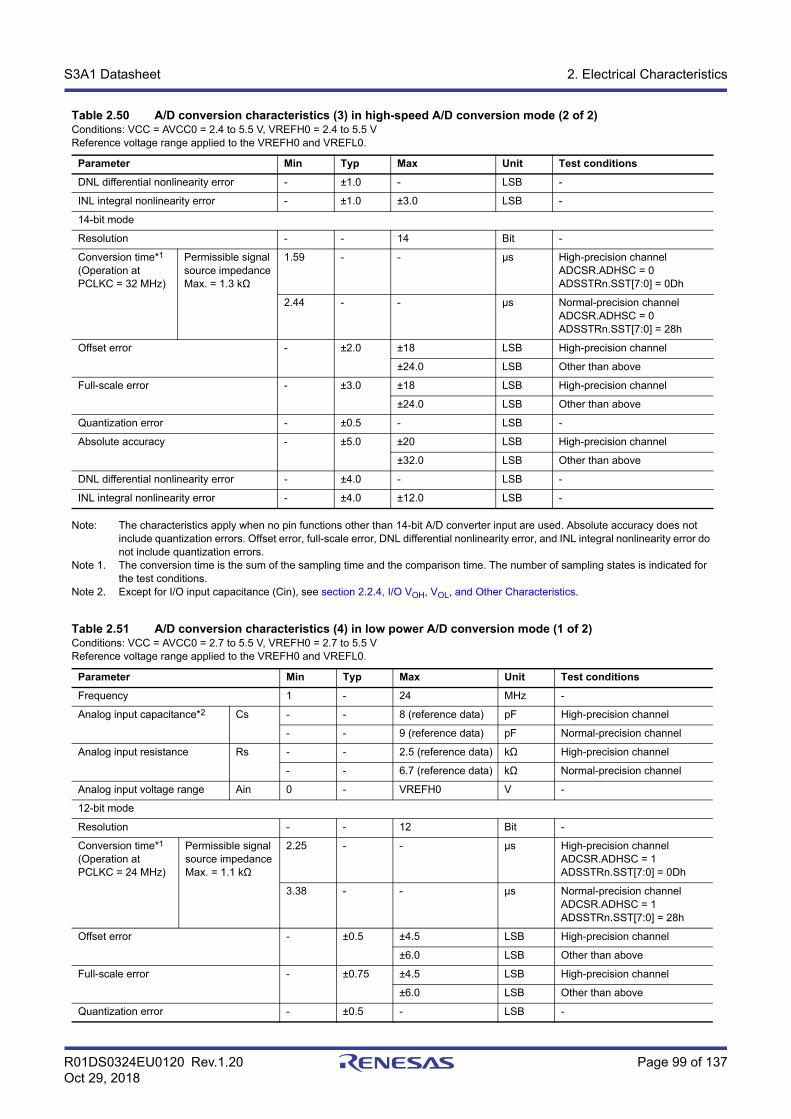
R01DS0324EU0120 Rev.1.20 Page 99 of 137Oct 29, 2018
S3A1 Datasheet 2. Electrical Characteristics
Note: The characteristics apply when no pin functions other than 14-bit A/D converter input are used. Absolute accuracy does not include quantization errors. Offset error, full-scale error, DNL differential nonlinearity error, and INL integral nonlinearity error do not include quantization errors.
Note 1. The conversion time is the sum of the sampling time and the comparison time. The number of sampling states is indicated for the test conditions.
Note 2. Except for I/O input capacitance (Cin), see section 2.2.4, I/O VOH, VOL, and Other Characteristics.
DNL differential nonlinearity error - ±1.0 - LSB -
INL integral nonlinearity error - ±1.0 ±3.0 LSB -
14-bit mode
Resolution - - 14 Bit -
Conversion time*1
(Operation at PCLKC = 32 MHz)
Permissible signal source impedance Max. = 1.3 kΩ
1.59 - - μs High-precision channelADCSR.ADHSC = 0ADSSTRn.SST[7:0] = 0Dh
2.44 - - μs Normal-precision channelADCSR.ADHSC = 0ADSSTRn.SST[7:0] = 28h
Offset error - ±2.0 ±18 LSB High-precision channel
±24.0 LSB Other than above
Full-scale error - ±3.0 ±18 LSB High-precision channel
±24.0 LSB Other than above
Quantization error - ±0.5 - LSB -
Absolute accuracy - ±5.0 ±20 LSB High-precision channel
±32.0 LSB Other than above
DNL differential nonlinearity error - ±4.0 - LSB -
INL integral nonlinearity error - ±4.0 ±12.0 LSB -
Table 2.51 A/D conversion characteristics (4) in low power A/D conversion mode (1 of 2)Conditions: VCC = AVCC0 = 2.7 to 5.5 V, VREFH0 = 2.7 to 5.5 VReference voltage range applied to the VREFH0 and VREFL0.
Parameter Min Typ Max Unit Test conditions
Frequency 1 - 24 MHz -
Analog input capacitance*2 Cs - - 8 (reference data) pF High-precision channel
- - 9 (reference data) pF Normal-precision channel
Analog input resistance Rs - - 2.5 (reference data) kΩ High-precision channel
- - 6.7 (reference data) kΩ Normal-precision channel
Analog input voltage range Ain 0 - VREFH0 V -
12-bit mode
Resolution - - 12 Bit -
Conversion time*1
(Operation at PCLKC = 24 MHz)
Permissible signal source impedance Max. = 1.1 kΩ
2.25 - - μs High-precision channelADCSR.ADHSC = 1ADSSTRn.SST[7:0] = 0Dh
3.38 - - μs Normal-precision channelADCSR.ADHSC = 1ADSSTRn.SST[7:0] = 28h
Offset error - ±0.5 ±4.5 LSB High-precision channel
±6.0 LSB Other than above
Full-scale error - ±0.75 ±4.5 LSB High-precision channel
±6.0 LSB Other than above
Quantization error - ±0.5 - LSB -
Table 2.50 A/D conversion characteristics (3) in high-speed A/D conversion mode (2 of 2)Conditions: VCC = AVCC0 = 2.4 to 5.5 V, VREFH0 = 2.4 to 5.5 VReference voltage range applied to the VREFH0 and VREFL0.
Parameter Min Typ Max Unit Test conditions
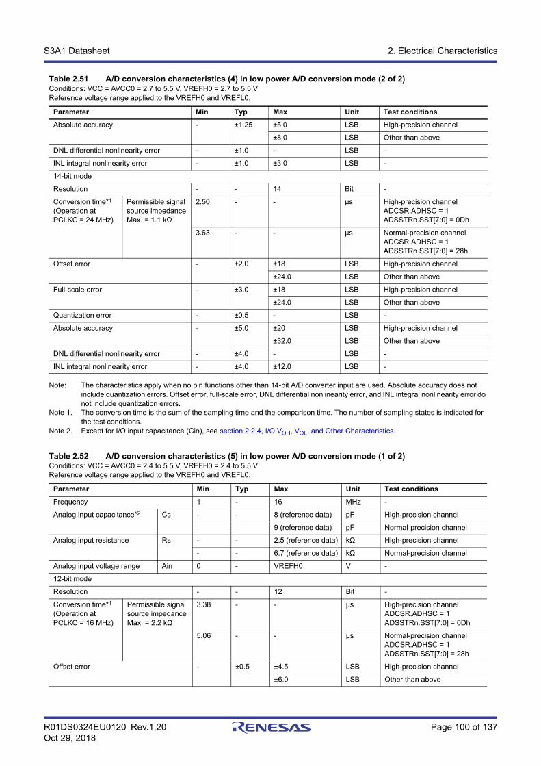
R01DS0324EU0120 Rev.1.20 Page 100 of 137Oct 29, 2018
S3A1 Datasheet 2. Electrical Characteristics
Note: The characteristics apply when no pin functions other than 14-bit A/D converter input are used. Absolute accuracy does not include quantization errors. Offset error, full-scale error, DNL differential nonlinearity error, and INL integral nonlinearity error do not include quantization errors.
Note 1. The conversion time is the sum of the sampling time and the comparison time. The number of sampling states is indicated for the test conditions.
Note 2. Except for I/O input capacitance (Cin), see section 2.2.4, I/O VOH, VOL, and Other Characteristics.
Absolute accuracy - ±1.25 ±5.0 LSB High-precision channel
±8.0 LSB Other than above
DNL differential nonlinearity error - ±1.0 - LSB -
INL integral nonlinearity error - ±1.0 ±3.0 LSB -
14-bit mode
Resolution - - 14 Bit -
Conversion time*1
(Operation at PCLKC = 24 MHz)
Permissible signal source impedance Max. = 1.1 kΩ
2.50 - - μs High-precision channelADCSR.ADHSC = 1ADSSTRn.SST[7:0] = 0Dh
3.63 - - μs Normal-precision channelADCSR.ADHSC = 1ADSSTRn.SST[7:0] = 28h
Offset error - ±2.0 ±18 LSB High-precision channel
±24.0 LSB Other than above
Full-scale error - ±3.0 ±18 LSB High-precision channel
±24.0 LSB Other than above
Quantization error - ±0.5 - LSB -
Absolute accuracy - ±5.0 ±20 LSB High-precision channel
±32.0 LSB Other than above
DNL differential nonlinearity error - ±4.0 - LSB -
INL integral nonlinearity error - ±4.0 ±12.0 LSB -
Table 2.52 A/D conversion characteristics (5) in low power A/D conversion mode (1 of 2)Conditions: VCC = AVCC0 = 2.4 to 5.5 V, VREFH0 = 2.4 to 5.5 VReference voltage range applied to the VREFH0 and VREFL0.
Parameter Min Typ Max Unit Test conditions
Frequency 1 - 16 MHz -
Analog input capacitance*2 Cs - - 8 (reference data) pF High-precision channel
- - 9 (reference data) pF Normal-precision channel
Analog input resistance Rs - - 2.5 (reference data) kΩ High-precision channel
- - 6.7 (reference data) kΩ Normal-precision channel
Analog input voltage range Ain 0 - VREFH0 V -
12-bit mode
Resolution - - 12 Bit -
Conversion time*1
(Operation at PCLKC = 16 MHz)
Permissible signal source impedance Max. = 2.2 kΩ
3.38 - - μs High-precision channelADCSR.ADHSC = 1ADSSTRn.SST[7:0] = 0Dh
5.06 - - μs Normal-precision channelADCSR.ADHSC = 1ADSSTRn.SST[7:0] = 28h
Offset error - ±0.5 ±4.5 LSB High-precision channel
±6.0 LSB Other than above
Table 2.51 A/D conversion characteristics (4) in low power A/D conversion mode (2 of 2)Conditions: VCC = AVCC0 = 2.7 to 5.5 V, VREFH0 = 2.7 to 5.5 VReference voltage range applied to the VREFH0 and VREFL0.
Parameter Min Typ Max Unit Test conditions
R01DS0324EU0120 Rev.1.20 Page 101 of 137Oct 29, 2018
S3A1 Datasheet 2. Electrical Characteristics
Note: The characteristics apply when no pin functions other than 14-bit A/D converter input are used. Absolute accuracy does not include quantization errors. Offset error, full-scale error, DNL differential nonlinearity error, and INL integral nonlinearity error do not include quantization errors.
Note 1. The conversion time is the sum of the sampling time and the comparison time. The number of sampling states is indicated for the test conditions.
Note 2. Except for I/O input capacitance (Cin), see section 2.2.4, I/O VOH, VOL, and Other Characteristics.
Full-scale error - ±0.75 ±4.5 LSB High-precision channel
±6.0 LSB Other than above
Quantization error - ±0.5 - LSB -
Absolute accuracy - ±1.25 ±5.0 LSB High-precision channel
±8.0 LSB Other than above
DNL differential nonlinearity error - ±1.0 - LSB -
INL integral nonlinearity error - ±1.0 ±3.0 LSB -
14-bit mode
Resolution - - 14 Bit -
Conversion time*1
(Operation at PCLKC = 16 MHz)
Permissible signal source impedance Max. = 2.2 kΩ
3.75 - - μs High-precision channelADCSR.ADHSC = 1ADSSTRn.SST[7:0] = 0Dh
5.44 - - μs Normal-precision channelADCSR.ADHSC = 1ADSSTRn.SST[7:0] = 28h
Offset error - ±2.0 ±18 LSB High-precision channel
±24.0 LSB Other than above
Full-scale error - ±3.0 ±18 LSB High-precision channel
±24.0 LSB Other than above
Quantization error - ±0.5 - LSB -
Absolute accuracy - ±5.0 ±20 LSB High-precision channel
±32.0 LSB Other than above
DNL differential nonlinearity error - ±4.0 - LSB -
INL integral nonlinearity error - ±4.0 ±12.0 LSB -
Table 2.53 A/D conversion characteristics (6) in low power A/D conversion mode (1 of 2)Conditions: VCC = AVCC0 = 1.8 to 5.5 V (AVCC0 = VCC when VCC < 2.0 V), VREFH0 = 1.8 to 5.5 VReference voltage range applied to the VREFH0 and VREFL0.
Parameter Min Typ Max Unit Test conditions
Frequency 1 - 8 MHz -
Analog input capacitance*2 Cs - - 8 (reference data) pF High-precision channel
- - 9 (reference data) pF Normal-precision channel
Analog input resistance Rs - - 3.8 (reference data) kΩ High-precision channel
- - 8.2 (reference data) kΩ Normal-precision channel
Analog input voltage range Ain 0 - VREFH0 V -
12-bit mode
Resolution - - 12 Bit -
Table 2.52 A/D conversion characteristics (5) in low power A/D conversion mode (2 of 2)Conditions: VCC = AVCC0 = 2.4 to 5.5 V, VREFH0 = 2.4 to 5.5 VReference voltage range applied to the VREFH0 and VREFL0.
Parameter Min Typ Max Unit Test conditions
R01DS0324EU0120 Rev.1.20 Page 102 of 137Oct 29, 2018
S3A1 Datasheet 2. Electrical Characteristics
Note: The characteristics apply when no pin functions other than 14-bit A/D converter input are used. Absolute accuracy does not include quantization errors. Offset error, full-scale error, DNL differential nonlinearity error, and INL integral nonlinearity error do not include quantization errors.
Note 1. The conversion time is the sum of the sampling time and the comparison time. The number of sampling states is indicated for the test conditions.
Note 2. Except for I/O input capacitance (Cin), see section 2.2.4, I/O VOH, VOL, and Other Characteristics.
Conversion time*1
(Operation at PCLKC = 8 MHz)
Permissible signal source impedance Max. = 5 kΩ
6.75 - - μs High-precision channelADCSR.ADHSC = 1ADSSTRn.SST[7:0] = 0Dh
10.13 - - μs Normal-precision channelADCSR.ADHSC = 1ADSSTRn.SST[7:0] = 28h
Offset error - ±1.0 ±7.5 LSB High-precision channel
±10.0 LSB Other than above
Full-scale error - ±1.5 ±7.5 LSB High-precision channel
±10.0 LSB Other than above
Quantization error - ±0.5 - LSB -
Absolute accuracy - ±3.0 ±8.0 LSB High-precision channel
±12.0 LSB Other than above
DNL differential nonlinearity error - ±1.0 - LSB -
INL integral nonlinearity error - ±1.0 ±3.0 LSB -
14-bit mode
Resolution - - 14 Bit -
Conversion time*1
(Operation at PCLKC = 8 MHz)
Permissible signal source impedance Max. = 5 kΩ
7.50 - - μs High-precision channelADCSR.ADHSC = 1ADSSTRn.SST[7:0] = 0Dh
10.88 - - μs Normal-precision channelADCSR.ADHSC = 1ADSSTRn.SST[7:0] = 28h
Offset error - ±4.0 ±30.0 LSB High-precision channel
±40.0 LSB Other than above
Full-scale error - ±6.0 ±30.0 LSB High-precision channel
±40.0 LSB Other than above
Quantization error - ±0.5 - LSB -
Absolute accuracy - ±12.0 ±32.0 LSB High-precision channel
±48.0 LSB Other than above
DNL differential nonlinearity error - ±4.0 - LSB -
INL integral nonlinearity error - ±4.0 ±12.0 LSB -
Table 2.53 A/D conversion characteristics (6) in low power A/D conversion mode (2 of 2)Conditions: VCC = AVCC0 = 1.8 to 5.5 V (AVCC0 = VCC when VCC < 2.0 V), VREFH0 = 1.8 to 5.5 VReference voltage range applied to the VREFH0 and VREFL0.
Parameter Min Typ Max Unit Test conditions
R01DS0324EU0120 Rev.1.20 Page 103 of 137Oct 29, 2018
S3A1 Datasheet 2. Electrical Characteristics
Note: The characteristics apply when no pin functions other than 14-bit A/D converter input are used. Absolute accuracy does not include quantization errors. Offset error, full-scale error, DNL differential nonlinearity error, and INL integral nonlinearity error do not include quantization errors.
Note 1. The conversion time is the sum of the sampling time and the comparison time. The number of sampling states is indicated for the test conditions.
Note 2. Except for I/O input capacitance (Cin), see section 2.2.4, I/O VOH, VOL, and Other Characteristics.
Table 2.54 A/D conversion characteristics (7) in low power A/D conversion modeConditions: VCC = AVCC0 = 1.6 to 5.5 V (AVCC0 = VCC when VCC < 2.0 V), VREFH0 = 1.6 to 5.5 VReference voltage range applied to the VREFH0 and VREFL0.
Parameter Min Typ Max Unit Test conditions
Frequency 1 - 4 MHz -
Analog input capacitance*2 Cs - - 8 (reference data) pF High-precision channel
- - 9 (reference data) pF Normal-precision channel
Analog input resistance Rs - - 13.1 (reference data) kΩ High-precision channel
- - 14.3 (reference data) kΩ Normal-precision channel
Analog input voltage range Ain 0 - VREFH0 V -
12-bit mode
Resolution - - 12 Bit -
Conversion time*1
(Operation at PCLKC = 4 MHz)
Permissible signal source impedance Max. = 9.9 kΩ
13.5 - - μs High-precision channelADCSR.ADHSC = 1ADSSTRn.SST[7:0] = 0Dh
20.25 - - μs Normal-precision channelADCSR.ADHSC = 1ADSSTRn.SST[7:0] = 28h
Offset error - ±1.0 ±7.5 LSB High-precision channel
±10.0 LSB Other than above
Full-scale error - ±1.5 ±7.5 LSB High-precision channel
±10.0 LSB Other than above
Quantization error - ±0.5 - LSB -
Absolute accuracy - ±3.0 ±8.0 LSB High-precision channel
±12.0 LSB Other than above
DNL differential nonlinearity error - ±1.0 - LSB -
INL integral nonlinearity error - ±1.0 ±3.0 LSB -
14-bit mode
Resolution - - 14 Bit -
Conversion time*1
(Operation at PCLKC = 4 MHz)
Permissible signal source impedance Max. = 9.9 kΩ
15.0 - - μs High-precision channelADCSR.ADHSC = 1ADSSTRn.SST[7:0] = 0Dh
21.75 - - μs Normal-precision channelADCSR.ADHSC = 1ADSSTRn.SST[7:0] = 28h
Offset error - ±4.0 ±30.0 LSB High-precision channel
±40.0 LSB Other than above
Full-scale error - ±6.0 ±30.0 LSB High-precision channel
±40.0 LSB Other than above
Quantization error - ±0.5 - LSB -
Absolute accuracy - ±12.0 ±32.0 LSB High-precision channel
±48.0 LSB Other than above
DNL differential nonlinearity error - ±4.0 - LSB -
INL integral nonlinearity error - ±4.0 ±12.0 LSB -
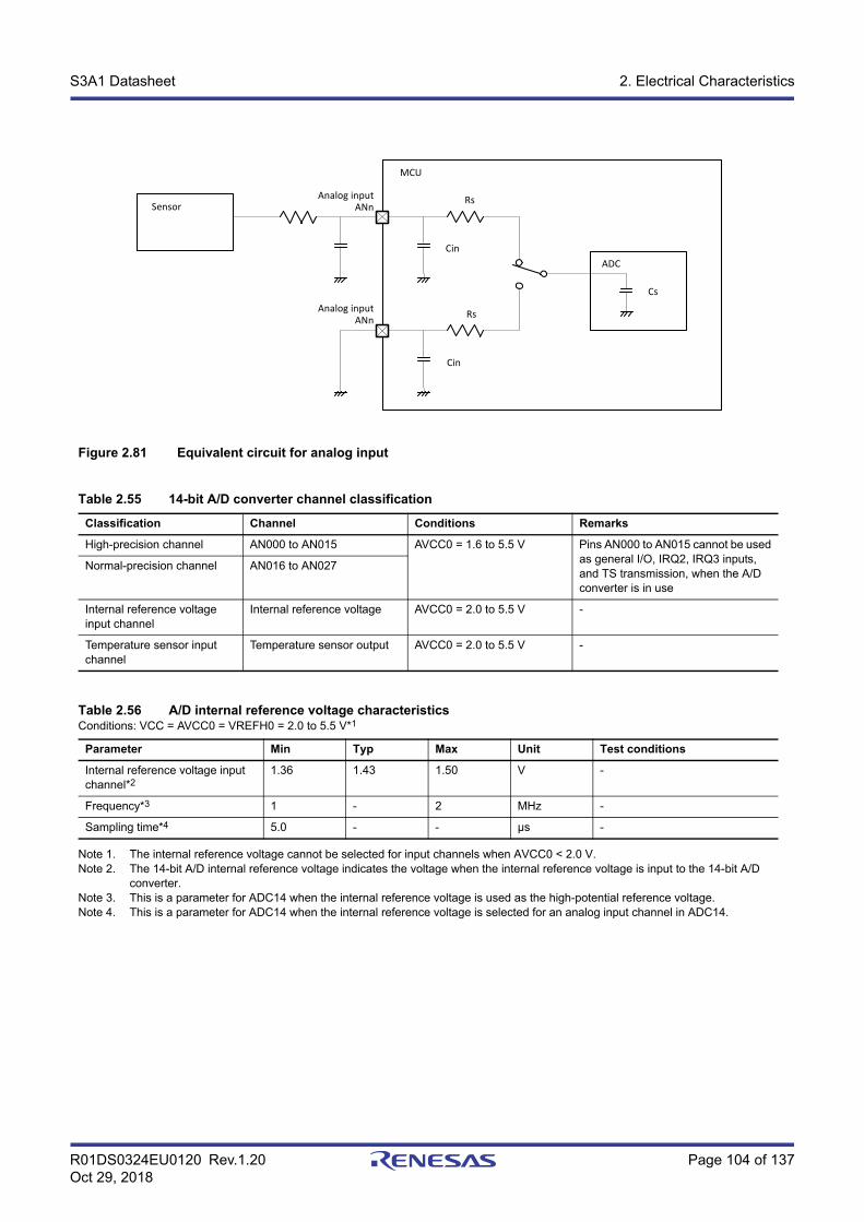
R01DS0324EU0120 Rev.1.20 Page 104 of 137Oct 29, 2018
S3A1 Datasheet 2. Electrical Characteristics
Figure 2.81 Equivalent circuit for analog input
Note 1. The internal reference voltage cannot be selected for input channels when AVCC0 < 2.0 V.Note 2. The 14-bit A/D internal reference voltage indicates the voltage when the internal reference voltage is input to the 14-bit A/D
converter.Note 3. This is a parameter for ADC14 when the internal reference voltage is used as the high-potential reference voltage.Note 4. This is a parameter for ADC14 when the internal reference voltage is selected for an analog input channel in ADC14.
Table 2.55 14-bit A/D converter channel classification
Classification Channel Conditions Remarks
High-precision channel AN000 to AN015 AVCC0 = 1.6 to 5.5 V Pins AN000 to AN015 cannot be used as general I/O, IRQ2, IRQ3 inputs, and TS transmission, when the A/D converter is in use
Normal-precision channel AN016 to AN027
Internal reference voltage input channel
Internal reference voltage AVCC0 = 2.0 to 5.5 V -
Temperature sensor input channel
Temperature sensor output AVCC0 = 2.0 to 5.5 V -
Table 2.56 A/D internal reference voltage characteristicsConditions: VCC = AVCC0 = VREFH0 = 2.0 to 5.5 V*1
Parameter Min Typ Max Unit Test conditions
Internal reference voltage input channel*2
1.36 1.43 1.50 V -
Frequency*3 1 - 2 MHz -
Sampling time*4 5.0 - - µs -
Rs
Cin
Rs
Cin
Cs
ADC
MCU
Analog input
Analog input
Sensor ANn
ANn
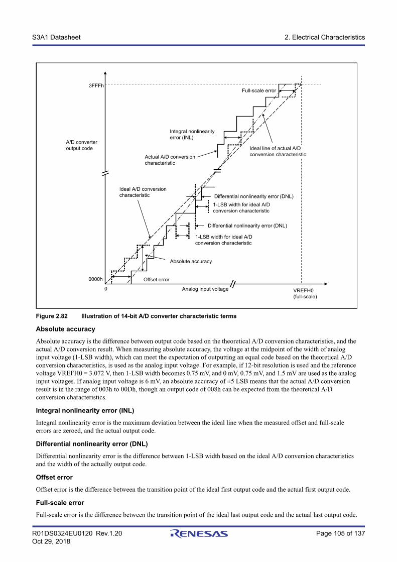
R01DS0324EU0120 Rev.1.20 Page 105 of 137Oct 29, 2018
S3A1 Datasheet 2. Electrical Characteristics
Figure 2.82 Illustration of 14-bit A/D converter characteristic terms
Absolute accuracy
Absolute accuracy is the difference between output code based on the theoretical A/D conversion characteristics, and the actual A/D conversion result. When measuring absolute accuracy, the voltage at the midpoint of the width of analog input voltage (1-LSB width), which can meet the expectation of outputting an equal code based on the theoretical A/D conversion characteristics, is used as the analog input voltage. For example, if 12-bit resolution is used and the reference voltage VREFH0 = 3.072 V, then 1-LSB width becomes 0.75 mV, and 0 mV, 0.75 mV, and 1.5 mV are used as the analog input voltages. If analog input voltage is 6 mV, an absolute accuracy of ±5 LSB means that the actual A/D conversion result is in the range of 003h to 00Dh, though an output code of 008h can be expected from the theoretical A/D conversion characteristics.
Integral nonlinearity error (INL)
Integral nonlinearity error is the maximum deviation between the ideal line when the measured offset and full-scale errors are zeroed, and the actual output code.
Differential nonlinearity error (DNL)
Differential nonlinearity error is the difference between 1-LSB width based on the ideal A/D conversion characteristics and the width of the actually output code.
Offset error
Offset error is the difference between the transition point of the ideal first output code and the actual first output code.
Full-scale error
Full-scale error is the difference between the transition point of the ideal last output code and the actual last output code.
Integral nonlinearity error (INL)
Actual A/D conversion characteristic
Ideal A/D conversion characteristic
Analog input voltage
Offset error
Absolute accuracy
Differential nonlinearity error (DNL)
Full-scale error3FFFh
0000h
0
Ideal line of actual A/D conversion characteristic
1-LSB width for ideal A/D conversion characteristic
Differential nonlinearity error (DNL)
1-LSB width for ideal A/D conversion characteristic
VREFH0(full-scale)
A/D converteroutput code
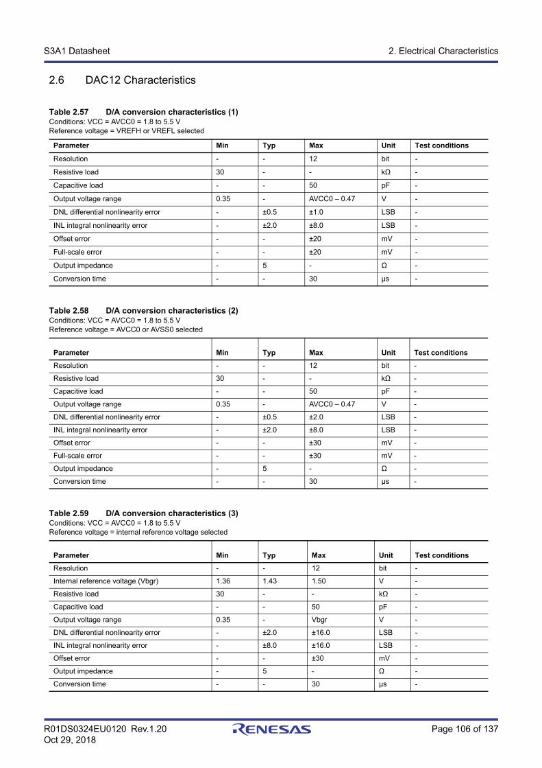
R01DS0324EU0120 Rev.1.20 Page 106 of 137Oct 29, 2018
S3A1 Datasheet 2. Electrical Characteristics
2.6 DAC12 Characteristics
Table 2.57 D/A conversion characteristics (1)Conditions: VCC = AVCC0 = 1.8 to 5.5 VReference voltage = VREFH or VREFL selected
Parameter Min Typ Max Unit Test conditions
Resolution - - 12 bit -
Resistive load 30 - - kΩ -
Capacitive load - - 50 pF -
Output voltage range 0.35 - AVCC0 – 0.47 V -
DNL differential nonlinearity error - ±0.5 ±1.0 LSB -
INL integral nonlinearity error - ±2.0 ±8.0 LSB -
Offset error - - ±20 mV -
Full-scale error - - ±20 mV -
Output impedance - 5 - Ω -
Conversion time - - 30 μs -
Table 2.58 D/A conversion characteristics (2)Conditions: VCC = AVCC0 = 1.8 to 5.5 VReference voltage = AVCC0 or AVSS0 selected
Parameter Min Typ Max Unit Test conditions
Resolution - - 12 bit -
Resistive load 30 - - kΩ -
Capacitive load - - 50 pF -
Output voltage range 0.35 - AVCC0 – 0.47 V -
DNL differential nonlinearity error - ±0.5 ±2.0 LSB -
INL integral nonlinearity error - ±2.0 ±8.0 LSB -
Offset error - - ±30 mV -
Full-scale error - - ±30 mV -
Output impedance - 5 - Ω -
Conversion time - - 30 μs -
Table 2.59 D/A conversion characteristics (3)Conditions: VCC = AVCC0 = 1.8 to 5.5 VReference voltage = internal reference voltage selected
Parameter Min Typ Max Unit Test conditions
Resolution - - 12 bit -
Internal reference voltage (Vbgr) 1.36 1.43 1.50 V -
Resistive load 30 - - kΩ -
Capacitive load - - 50 pF -
Output voltage range 0.35 - Vbgr V -
DNL differential nonlinearity error - ±2.0 ±16.0 LSB -
INL integral nonlinearity error - ±8.0 ±16.0 LSB -
Offset error - - ±30 mV -
Output impedance - 5 - Ω -
Conversion time - - 30 μs -
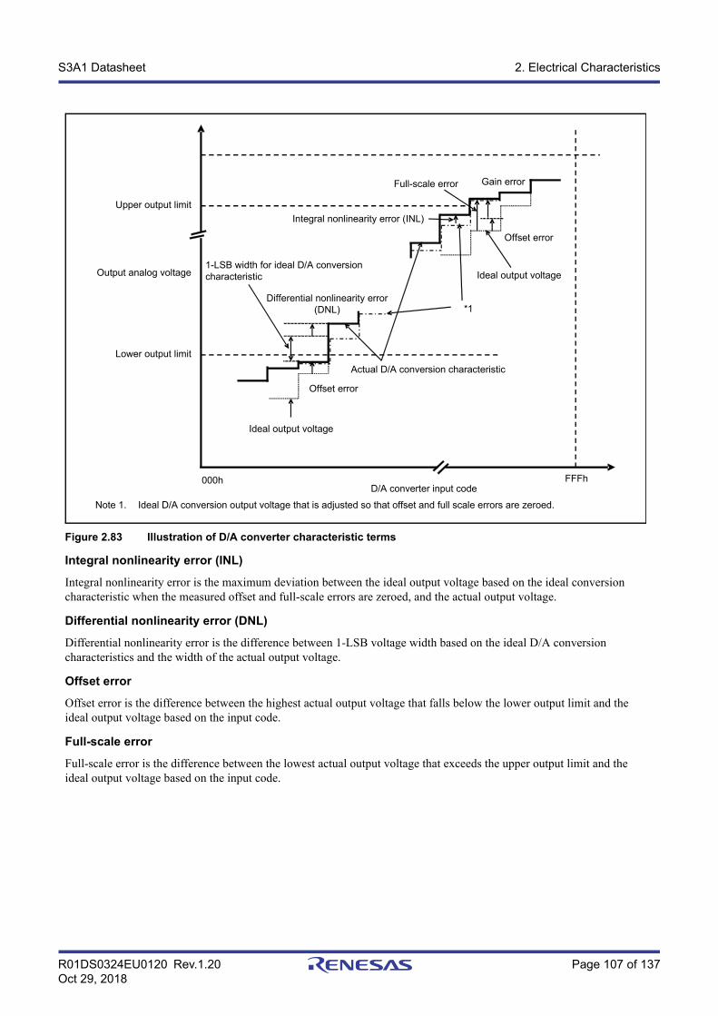
R01DS0324EU0120 Rev.1.20 Page 107 of 137Oct 29, 2018
S3A1 Datasheet 2. Electrical Characteristics
Figure 2.83 Illustration of D/A converter characteristic terms
Integral nonlinearity error (INL)
Integral nonlinearity error is the maximum deviation between the ideal output voltage based on the ideal conversion characteristic when the measured offset and full-scale errors are zeroed, and the actual output voltage.
Differential nonlinearity error (DNL)
Differential nonlinearity error is the difference between 1-LSB voltage width based on the ideal D/A conversion characteristics and the width of the actual output voltage.
Offset error
Offset error is the difference between the highest actual output voltage that falls below the lower output limit and the ideal output voltage based on the input code.
Full-scale error
Full-scale error is the difference between the lowest actual output voltage that exceeds the upper output limit and the ideal output voltage based on the input code.
000hD/A converter input code
FFFh
Output analog voltage
Upper output limit
Lower output limit
Offset error
Ideal output voltage
1-LSB width for ideal D/A conversion characteristic
Differential nonlinearity error (DNL)
Actual D/A conversion characteristic
*1
Integral nonlinearity error (INL)
Full-scale error Gain error
Offset error
Ideal output voltage
Note 1. Ideal D/A conversion output voltage that is adjusted so that offset and full scale errors are zeroed.
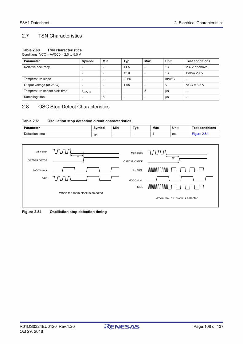
R01DS0324EU0120 Rev.1.20 Page 108 of 137Oct 29, 2018
S3A1 Datasheet 2. Electrical Characteristics
2.7 TSN Characteristics
2.8 OSC Stop Detect Characteristics
Figure 2.84 Oscillation stop detection timing
Table 2.60 TSN characteristicsConditions: VCC = AVCC0 = 2.0 to 5.5 V
Parameter Symbol Min Typ Max Unit Test conditions
Relative accuracy - - ±1.5 - °C 2.4 V or above
- - ±2.0 - °C Below 2.4 V
Temperature slope - - -3.65 - mV/°C -
Output voltage (at 25°C) - - 1.05 - V VCC = 3.3 V
Temperature sensor start time tSTART - - 5 μs -
Sampling time - 5 - - μs -
Table 2.61 Oscillation stop detection circuit characteristics
Parameter Symbol Min Typ Max Unit Test conditions
Detection time tdr - - 1 ms Figure 2.84
tdr
Main clock
OSTDSR.OSTDF
MOCO clock
ICLK
PLL clock
tdr
Main clock
OSTDSR.OSTDF
MOCO clock
ICLK
When the main clock is selected
When the PLL clock is selected
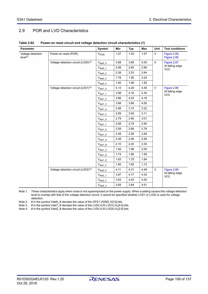
R01DS0324EU0120 Rev.1.20 Page 109 of 137Oct 29, 2018
S3A1 Datasheet 2. Electrical Characteristics
2.9 POR and LVD Characteristics
Note 1. These characteristics apply when noise is not superimposed on the power supply. When a setting causes this voltage detection level to overlap with that of the voltage detection circuit, it cannot be specified whether LVD1 or LVD2 is used for voltage detection.
Note 2. # in the symbol Vdet0_# denotes the value of the OFS1.VDSEL1[2:0] bits.Note 3. # in the symbol Vdet1_# denotes the value of the LVDLVLR.LVD1LVL[4:0] bits.Note 4. # in the symbol Vdet2_# denotes the value of the LVDLVLR.LVD2LVL[2:0] bits.
Table 2.62 Power-on reset circuit and voltage detection circuit characteristics (1)
Parameter Symbol Min Typ Max Unit Test conditions
Voltage detection level*1
Power-on reset (POR) VPOR 1.27 1.42 1.57 V Figure 2.85, Figure 2.86
Voltage detection circuit (LVD0)*2 Vdet0_0 3.68 3.85 4.00 V Figure 2.87At falling edge VCC
Vdet0_1 2.68 2.85 2.96
Vdet0_2 2.38 2.53 2.64
Vdet0_3 1.78 1.90 2.02
Vdet0_4 1.60 1.69 1.82
Voltage detection circuit (LVD1)*3 Vdet1_0 4.13 4.29 4.45 V Figure 2.88At falling edge VCC
Vdet1_1 3.98 4.16 4.30
Vdet1_2 3.86 4.03 4.18
Vdet1_3 3.68 3.86 4.00
Vdet1_4 2.98 3.10 3.22
Vdet1_5 2.89 3.00 3.11
Vdet1_6 2.79 2.90 3.01
Vdet1_7 2.68 2.79 2.90
Vdet1_8 2.58 2.68 2.78
Vdet1_9 2.48 2.58 2.68
Vdet1_A 2.38 2.48 2.58
Vdet1_B 2.10 2.20 2.30
Vdet1_C 1.84 1.96 2.05
Vdet1_D 1.74 1.86 1.95
Vdet1_E 1.63 1.75 1.84
Vdet1_F 1.60 1.65 1.73
Voltage detection circuit (LVD2)*4 Vdet2_0 4.11 4.31 4.48 V Figure 2.89At falling edge VCC
Vdet2_1 3.97 4.17 4.34
Vdet2_2 3.83 4.03 4.20
Vdet2_3 3.64 3.84 4.01
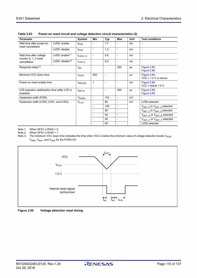
R01DS0324EU0120 Rev.1.20 Page 110 of 137Oct 29, 2018
S3A1 Datasheet 2. Electrical Characteristics
Note 1. When OFS1.LVDAS = 0.Note 2. When OFS1.LVDAS = 1.Note 3. The minimum VCC down time indicates the time when VCC is below the minimum value of voltage detection levels VPOR,
Vdet0, Vdet1, and Vdet2 for the POR/LVD.
Figure 2.85 Voltage detection reset timing
Table 2.63 Power-on reset circuit and voltage detection circuit characteristics (2)
Parameter Symbol Min Typ Max Unit Test conditions
Wait time after power-on reset cancellation
LVD0: enable tPOR - 1.7 - ms -
LVD0: disable tPOR - 1.3 - ms -
Wait time after voltage monitor 0, 1, 2 reset cancellation
LVD0: enable*1 tLVD0,1,2 - 0.6 - ms -
LVD0: disable*2 tLVD1,2 - 0.2 - ms -
Response delay*3 tdet - - 350 μs Figure 2.85,Figure 2.86
Minimum VCC down time tVOFF 450 - - μs Figure 2.85,VCC = 1.0 V or above
Power-on reset enable time tW(POR) 1 - - ms Figure 2.86,VCC = below 1.0 V
LVD operation stabilization time (after LVD is enabled)
td(E-A) - - 300 μs Figure 2.88,Figure 2.89
Hysteresis width (POR) VPORH - 110 - mV -
Hysteresis width (LVD0, LVD1, and LVD2) VLVH - 60 - mV LVD0 selected
- 100 - Vdet1_0 to Vdet1_2 selected
- 60 - Vdet1_3 to Vdet1_9 selected
- 50 - Vdet1_A or Vdet1_B selected
- 40 - Vdet1_C or Vdet1_F selected
- 60 - LVD2 selected
Internal reset signal(active-low)
VCC
tVOFF
tPORtdet
VPOR
tdet
1.0 V
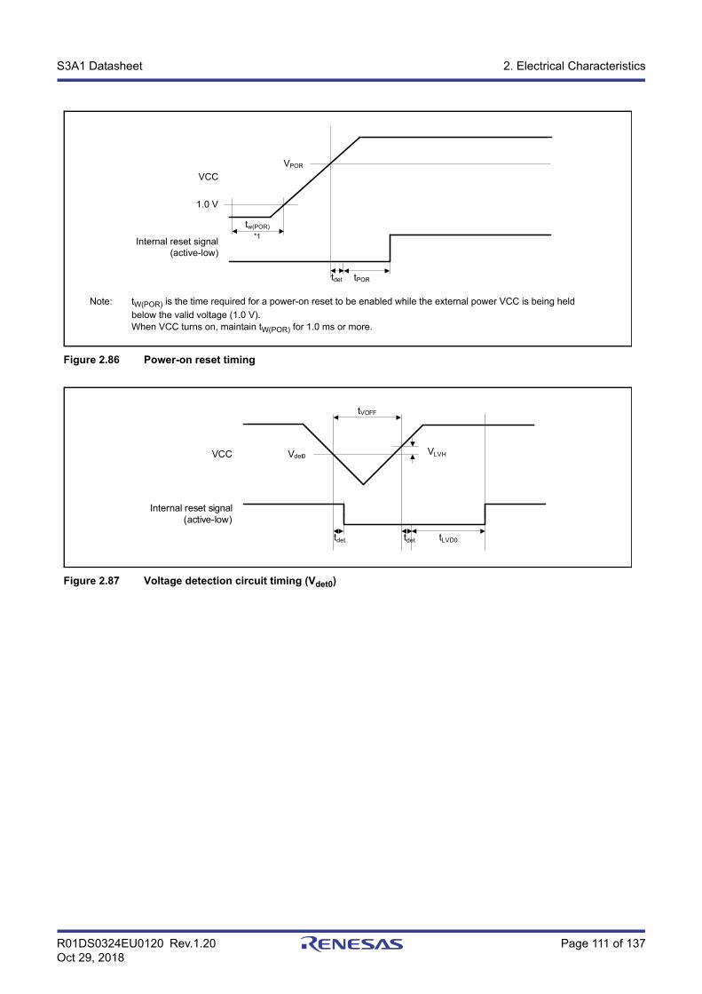
R01DS0324EU0120 Rev.1.20 Page 111 of 137Oct 29, 2018
S3A1 Datasheet 2. Electrical Characteristics
Figure 2.86 Power-on reset timing
Figure 2.87 Voltage detection circuit timing (Vdet0)
Note: tW(POR) is the time required for a power-on reset to be enabled while the external power VCC is being held
below the valid voltage (1.0 V).When VCC turns on, maintain tW(POR) for 1.0 ms or more.
Internal reset signal(active-low)
VCC
tPOR
VPOR
1.0 V
tw(POR)
*1
tdet
tVOFF
tLVD0tdet
Vdet0VCC
Internal reset signal(active-low)
tdet
VLVH
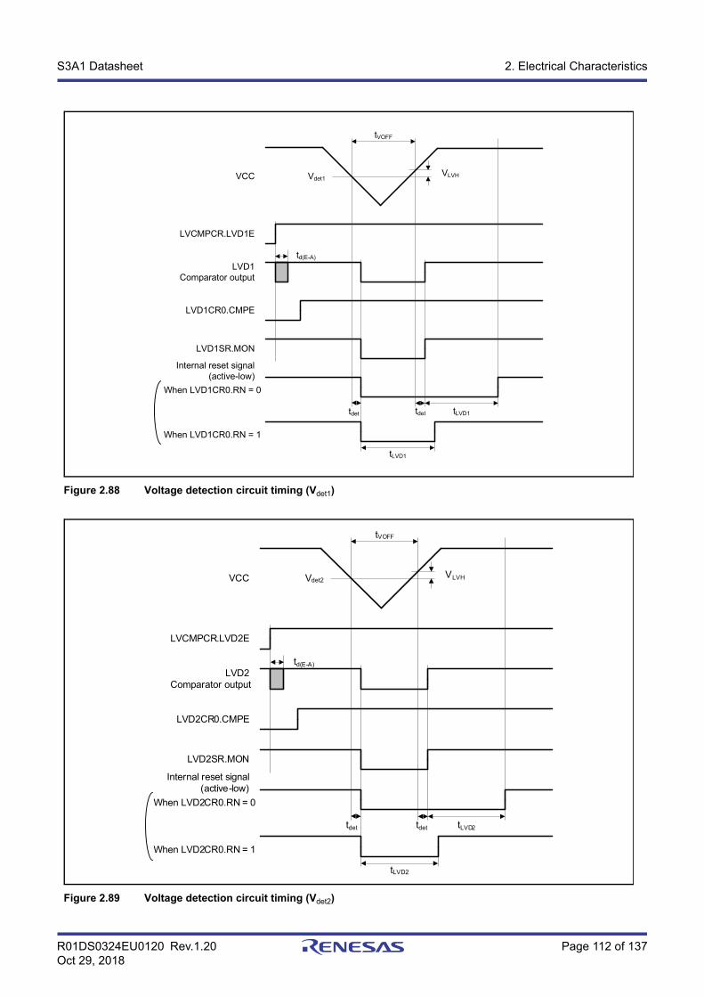
R01DS0324EU0120 Rev.1.20 Page 112 of 137Oct 29, 2018
S3A1 Datasheet 2. Electrical Characteristics
Figure 2.88 Voltage detection circuit timing (Vdet1)
Figure 2.89 Voltage detection circuit timing (Vdet2)
tVOFF
Vdet1VCC
tdettdet
tLVD1
td(E-A)
LVCMPCR.LVD1E
LVD1Comparator output
LVD1CR0.CMPE
LVD1SR.MON
Internal reset signal(active-low)
When LVD1CR0.RN = 0
When LVD1CR0.RN = 1
VLVH
tLVD1
tVOFF
Vdet2VCC
tdettdet
tLVD2
td(E-A)
LVCMPCR.LVD2E
LVD2Comparator output
LVD2CR0.CMPE
LVD2SR.MON
Internal reset signal (active-low)
When LVD2CR0.RN = 0
When LVD2CR0.RN = 1
VLVH
tLVD2
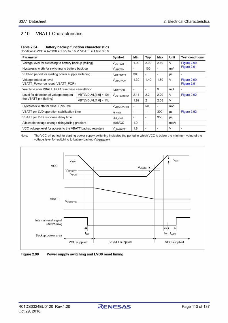
R01DS0324EU0120 Rev.1.20 Page 113 of 137Oct 29, 2018
S3A1 Datasheet 2. Electrical Characteristics
2.10 VBATT Characteristics
Note: The VCC-off period for starting power supply switching indicates the period in which VCC is below the minimum value of the voltage level for switching to battery backup (VDETBATT).
Figure 2.90 Power supply switching and LVD0 reset timing
Table 2.64 Battery backup function characteristicsConditions: VCC = AVCC0 = 1.6 V to 5.5 V, VBATT = 1.6 to 3.6 V
Parameter Symbol Min Typ Max Unit Test conditions
Voltage level for switching to battery backup (falling) VDETBATT 1.99 2.09 2.19 V Figure 2.90, Figure 2.91
Hysteresis width for switching to battery back up VVBATTH - 100 - mV
VCC-off period for starting power supply switching tVOFFBATT 300 - - μs -
Voltage detection level VBATT_Power-on reset (VBATT_POR)
VVBATPOR 1.30 1.40 1.50 V Figure 2.90, Figure 2.91
Wait time after VBATT_POR reset time cancellation tVBATPOR - - 3 mS -
Level for detection of voltage drop on the VBATT pin (falling)
VBTLVDLVL[1:0] = 10b VDETBATLVD 2.11 2.2 2.29 V Figure 2.92
VBTLVDLVL[1:0] = 11b 1.92 2 2.08 V
Hysteresis width for VBATT pin LVD VVBATLVDTH - 50 - mV
VBATT pin LVD operation stabilization time td_vbat - - 300 μs Figure 2.92
VBATT pin LVD response delay time tdet_vbat - - 350 μs
Allowable voltage change rising/falling gradient dt/dVCC 1.0 - - ms/V -
VCC voltage level for access to the VBATT backup registers V_BKBATT 1.8 - - V -
VDETBATT
VVBATH
VCC supplied
VBATT
VCC
VVBATPOR
VBATT supplied VCC supplied
Backup power area
Internal reset signal(active-low)
tLVD0
Vdet0VLVH
tdettdet
VPOR
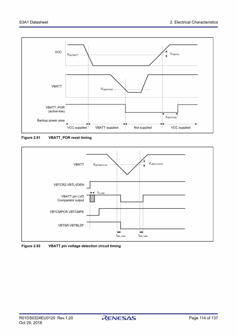
R01DS0324EU0120 Rev.1.20 Page 114 of 137Oct 29, 2018
S3A1 Datasheet 2. Electrical Characteristics
Figure 2.91 VBATT_POR reset timing
Figure 2.92 VBATT pin voltage detection circuit timing
VDETBATT VVBATH
VCC supplied
VBATT
VCC
VVBATPOR
VBATT supplied VCC supplied
Backup power area
Not supplied
VBATT_POR(active-low)
tVBATPOR
VDETBATLVDVBATT
td_vbat
VBTCR2.VBTLVDEN
VBATT pin LVDComparator output
VBTCMPCR.VBTCMPE
VBTSR.VBTBLDF
VVBATLVDTH
tdet_vbat tdet_vbat
R01DS0324EU0120 Rev.1.20 Page 115 of 137Oct 29, 2018
S3A1 Datasheet 2. Electrical Characteristics
2.11 CTSU Characteristics
2.12 Segment LCD Controller Characteristics
2.12.1 Resistance Division Method
[Static Display Mode]
[1/2 Bias Method, 1/4 Bias Method]
[1/3 Bias Method]
Table 2.65 VBATT-I/O characteristics
Parameter Symbol Min Typ Max Unit Test conditions
VBATWIOn I/O output characteristics(n = 0 to 2)
VCC > VDETBATT VCC = 4.0 to 5.5 V VOH VCC - 0.8 - - V IOH = -200 µA
VOL - - 0.8 IOL = 200 µA
VCC = 2.7 to 4.0 V VOH VCC - 0.5 - - IOH = -100 µA
VOL - - 0.5 IOL = 100 µA
VCC = VDETBATT to 2.7 V VOH VCC - 0.3 - - IOH = -50 µA
VOL - - 0.3 IOL = 50 µA
VCC < VDETBATT VBATT = 2.7 to 3.6 V VOH VBATT - 0.5 - - IOH = -100 µA
VOL - - 0.5 IOL = 100 µA
VBATT = 1.6 to 2.7 V VOH VBATT - 0.3 - - IOH = -50 µA
VOL - - 0.3 IOL = 50 µA
Table 2.66 CTSU characteristicsConditions: VCC = AVCC0 = 1.8 to 5.5 V
Parameter Symbol Min Typ Max Unit Test conditions
External capacitance connected to TSCAP pin Ctscap 9 10 11 nF -
TS pin capacitive load Cbase - - 50 pF -
Permissible output high current ΣIoH - - -24 mA When the mutual capacitance method is applied
Table 2.67 Resistance division method LCD characteristics (1)Conditions: VL4 ≤ VCC ≤ 5.5 V
Parameter Symbol Min Typ Max Unit Test conditions
LCD drive voltage VL4 2.0 - VCC V -
Table 2.68 Resistance division method LCD characteristics (2)Conditions: VL4 ≤ VCC ≤ 5.5 V
Parameter Symbol Min Typ Max Unit Test conditions
LCD drive voltage VL4 2.7 - VCC V -
Table 2.69 Resistance division method LCD characteristics (3)Conditions: VL4 ≤ VCC ≤ 5.5 V
Parameter Symbol Min Typ Max Unit Test conditions
LCD drive voltage VL4 2.5 - VCC V -
R01DS0324EU0120 Rev.1.20 Page 116 of 137Oct 29, 2018
S3A1 Datasheet 2. Electrical Characteristics
2.12.2 Internal Voltage Boosting Method
[1/3 Bias Method]
Note 1. This is a capacitor that is connected between voltage pins used to drive the LCD. C1: A capacitor connected between CAPH and CAPL C2: A capacitor connected between VL1 and GND C3: A capacitor connected between VL2 and GND C4: A capacitor connected between VL4 and GND C1 = C2 = C3 = C4 = 0.47 μF ± 30%
Note 2. This is the time required to wait from when the reference voltage is specified using the VLCD register (or when the internal voltage boosting method is selected (by setting the MDSET[1:0] bits in the LCDM0 register to 01b) if the default value reference voltage is used) until voltage boosting starts (VLCON = 1).
Note 3. This is the wait time from when voltage boosting is started (VLCON = 1) until display is enabled (LCDON = 1).
Table 2.70 Internal voltage boosting method LCD characteristicsConditions: VCC = 1.8 V to 5.5 V
Parameter Symbol Conditions Min Typ Max UnitTest conditions
LCD output voltage variation range
VL1 C1 to C4*1 = 0.47 μF VLCD = 04h 0.90 1.0 1.08 V -
VLCD = 05h 0.95 1.05 1.13 V -
VLCD = 06h 1.00 1.10 1.18 V -
VLCD = 07h 1.05 1.15 1.23 V -
VLCD = 08h 1.10 1.20 1.28 V -
VLCD = 09h 1.15 1.25 1.33 V -
VLCD = 0Ah 1.20 1.30 1.38 V -
VLCD = 0Bh 1.25 1.35 1.43 V -
VLCD = 0Ch 1.30 1.40 1.48 V -
VLCD = 0Dh 1.35 1.45 1.53 V -
VLCD = 0Eh 1.40 1.50 1.58 V -
VLCD = 0Fh 1.45 1.55 1.63 V -
VLCD = 10h 1.50 1.60 1.68 V -
VLCD = 11h 1.55 1.65 1.73 V -
VLCD = 12h 1.60 1.70 1.78 V -
VLCD = 13h 1.65 1.75 1.83 V -
Doubler output voltage VL2 C1 to C4*1 = 0.47 μF 2 × VL1 - 0.1 2 × VL1 2 × VL1 V -
Tripler output voltage VL4 C1 to C4*1 = 0.47 μF 3 × VL1 - 0.15 3 × VL1 3 × VL1 V -
Reference voltage setup time*2
tVL1S 5 - - ms Figure 2.93
LCD output voltage variation range*3
tVLWT C1 to C4*1 = 0.47 μF 500 - - ms
R01DS0324EU0120 Rev.1.20 Page 117 of 137Oct 29, 2018
S3A1 Datasheet 2. Electrical Characteristics
[1/4 Bias Method]
Note 1. This is a capacitor that is connected between voltage pins used to drive the LCD.C1: A capacitor connected between CAPH and CAPL C2: A capacitor connected between VL1 and GND C3: A capacitor connected between VL2 and GND C4: A capacitor connected between VL3 and GND C5: A capacitor connected between VL4 and GNDC1 = C2 = C3 = C4 = C5 = 0.47 μF ± 30%
Note 2. This is the time required to wait from when the reference voltage is specified by using the VLCD register or when the internal voltage boosting method is selected (by setting the MDSET[1] and MDSET[0] bits in the LCDM0 register to 01b) if the default value reference voltage is used) until voltage boosting starts (VLCON = 1).
Note 3. This is the wait time from when voltage boosting is started (VLCON = 1) until display is enabled (LCDON = 1).Note 4. VL4 must be 5.5 V or lower.
2.12.3 Capacitor Split Method
[1/3 Bias Method]
Note 1. This is the wait time from when voltage bucking is started (VLCON = 1) until display is enabled (LCDON = 1).Note 2. This is a capacitor that is connected between voltage pins used to drive the LCD.
C1: A capacitor connected between CAPH and CAPL C2: A capacitor connected between VL1 and GND C3: A capacitor connected between VL2 and GND C4: A capacitor connected between VL4 and GND C1 = C2 = C3 = C4 = 0.47 μF ± 30%.
Table 2.71 Internal voltage boosting method LCD characteristicsConditions: VCC = 1.8 V to 5.5 V
Parameter Symbol Conditions Min Typ Max UnitTest conditions
LCD output voltage variation range
VL1 C1 to C5*1 = 0.47 μF VLCD = 04h 0.90 1.0 1.08 V -
VLCD = 05h 0.95 1.05 1.13 V -
VLCD = 06h 1.00 1.10 1.18 V -
VLCD = 07h 1.05 1.15 1.23 V -
VLCD = 08h 1.10 1.20 1.28 V -
VLCD = 09h 1.15 1.25 1.33 V -
VLCD = 0Ah 1.20 1.30 1.38 V -
VLCD = 0Bh 1.25 1.35 1.43 V -
VLCD = 0Ch 1.30 1.40 1.48 V -
Doubler output voltage VL2 C1 to C5*1 = 0.47 μF 2VL1 - 0.08 2VL1 2VL1 V -
Tripler output voltage VL3 C1 to C5*1 = 0.47 μF 3VL1 - 0.12 3VL1 3VL1 V -
Quadruply output voltage
VL4*4 C1 to C5*1 = 0.47 μF 4VL1 - 0.16 4VL1 4VL1 V -
Reference voltage setup time*2
tVL1S 5 - - ms Figure 2.93
LCD output voltage variation range*3
tVLWT C1 to C5*1 = 0.47 μF 500 - - ms
Table 2.72 Internal voltage boosting method LCD characteristicsConditions: VCC = 2.2 V to 5.5 V
Parameter Symbol Conditions Min Typ Max UnitTest conditions
VL4 voltage*1 VL4 C1 to C4 = 0.47 μF*2 - VCC - V -
VL2 voltage*1 VL2 C1 to C4 = 0.47 μF*2 2/3 × VL4 - 0.07 2/3 × VL4 2/3 × VL4 + 0.07 V -
VL1 voltage*1 VL1 C1 to C4 = 0.47 μF*2 1/3 × VL4 - 0.08 1/3 × VL4 1/3 × VL4 + 0.08 V -
Capacitor split wait time*1 tWAIT 100 - - ms Figure 2.93
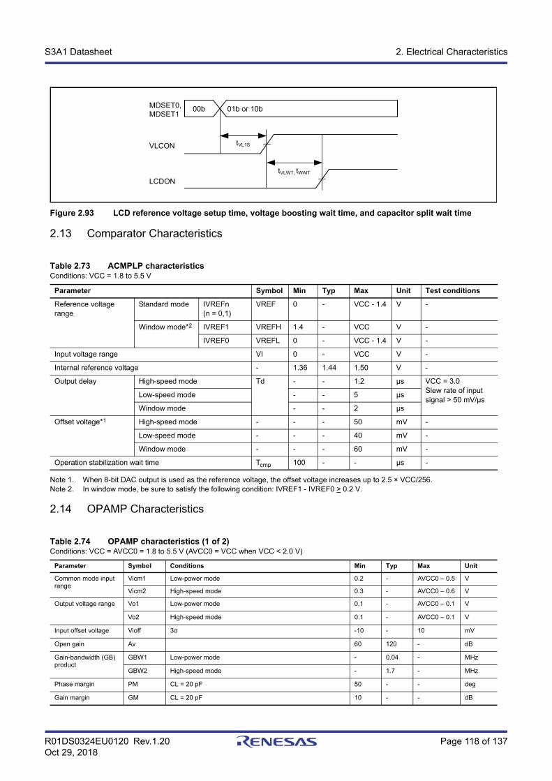
R01DS0324EU0120 Rev.1.20 Page 118 of 137Oct 29, 2018
S3A1 Datasheet 2. Electrical Characteristics
Figure 2.93 LCD reference voltage setup time, voltage boosting wait time, and capacitor split wait time
2.13 Comparator Characteristics
Note 1. When 8-bit DAC output is used as the reference voltage, the offset voltage increases up to 2.5 × VCC/256.Note 2. In window mode, be sure to satisfy the following condition: IVREF1 - IVREF0 > 0.2 V.
2.14 OPAMP Characteristics
Table 2.73 ACMPLP characteristicsConditions: VCC = 1.8 to 5.5 V
Parameter Symbol Min Typ Max Unit Test conditions
Reference voltage range
Standard mode IVREFn (n = 0,1)
VREF 0 - VCC - 1.4 V -
Window mode*2 IVREF1 VREFH 1.4 - VCC V -
IVREF0 VREFL 0 - VCC - 1.4 V -
Input voltage range VI 0 - VCC V -
Internal reference voltage - 1.36 1.44 1.50 V -
Output delay High-speed mode Td - - 1.2 μs VCC = 3.0Slew rate of input signal > 50 mV/μs
Low-speed mode - - 5 μs
Window mode - - 2 μs
Offset voltage*1 High-speed mode - - - 50 mV -
Low-speed mode - - - 40 mV -
Window mode - - - 60 mV -
Operation stabilization wait time Tcmp 100 - - μs -
Table 2.74 OPAMP characteristics (1 of 2)Conditions: VCC = AVCC0 = 1.8 to 5.5 V (AVCC0 = VCC when VCC < 2.0 V)
Parameter Symbol Conditions Min Typ Max Unit
Common mode input range
Vicm1 Low-power mode 0.2 - AVCC0 – 0.5 V
Vicm2 High-speed mode 0.3 - AVCC0 – 0.6 V
Output voltage range Vo1 Low-power mode 0.1 - AVCC0 – 0.1 V
Vo2 High-speed mode 0.1 - AVCC0 – 0.1 V
Input offset voltage Vioff 3σ -10 - 10 mV
Open gain Av 60 120 - dB
Gain-bandwidth (GB) product
GBW1 Low-power mode - 0.04 - MHz
GBW2 High-speed mode - 1.7 - MHz
Phase margin PM CL = 20 pF 50 - - deg
Gain margin GM CL = 20 pF 10 - - dB
MDSET0, MDSET1
VLCON
LCDON
01b or 10b00b
tVL1S
tVLWT, tWAIT
R01DS0324EU0120 Rev.1.20 Page 119 of 137Oct 29, 2018
S3A1 Datasheet 2. Electrical Characteristics
Note 1. When the operational amplifier reference current circuit is activated in advance.
2.15 Flash Memory Characteristics
2.15.1 Code Flash Memory Characteristics
Note 1. The reprogram/erase cycle is the number of erasures for each block. When the reprogram/erase cycle is n times (n = 1000), erasing can be done n times for each block. For instance, when 8-byte programming is performed 256 times for different addresses in 2-KB blocks, and the entire block is erased, the reprogram/erase cycle is counted as one. However, programming the same address for several times as one erasure is not enabled (overwriting is prohibited).
Note 2. Characteristic when using the flash memory programmer and the self-programming library provided by Renesas Electronics.Note 3. This result is obtained from reliability testing.
Equivalent input noise Vnoise1 f = 1 kHz Low power mode - 230 - nV/√Hz
Vnoise2 f = 10 kHz - 200 - nV/√Hz
Vnoise3 f = 1 kHz High-speed mode - 90 - nV/√Hz
Vnoise4 f = 2 kHz - 70 - nV/√Hz
Power supply reduction ratio
PSRR - 90 - dB
Common mode signal reduction ratio
CMRR - 90 - dB
Stabilization wait time Tstd1 CL = 20 pFOnly operational amplifier is activated *1
Low power mode 650 - - μs
Tstd2 High-speed mode 13 - - μs
Tstd3 CL = 20 pFOperational amplifier and reference current circuit are activated simultaneously
Low power mode 650 - - μs
Tstd4 High-speed mode 13 - - μs
Settling time Tset1 CL = 20 pF Low power mode - - 750 μs
Tset2 High-speed mode - - 13 μs
Slew rate Tslew1 CL = 20 pF Low power mode - 0.02 - V/μs
Tslew2 High-speed mode - 1.1 - V/μs
Load current Iload1 Low power mode -100 - 100 μA
Iload2 High-speed mode -100 - 100 μA
Load capacitance CL - - 20 pF
Table 2.75 Code flash characteristics (1)
Parameter Symbol Min Typ Max Unit Test conditions
Reprogramming/erasure cycle*1 NPEC 1000 - - Times -
Data hold time After 1000 times of NPEC tDRP 20*2, *3 - - Year Ta = +85°C
Table 2.76 Code flash characteristics (2) (1 of 2)High-speed operating modeConditions: VCC = 2.7 to 5.5 V
Parameter Symbol
FCLK = 1 MHz FCLK = 32 MHz
UnitMin Typ Max Min Typ Max
Programming time 8-byte tP8 - 116 998 - 54 506 μs
Erasure time 2-KB tE2K - 9.03 287 - 5.67 222 ms
Blank check time 8-byte tBC8 - - 56.8 - - 16.6 μs
2-KB tBC2K - - 1899 - - 140 μs
Erase suspended time tSED - - 22.5 - - 10.7 μs
Startup area switching setting time tSAS - 21.7 585 - 12.1 447 ms
Access window time tAWS - 21.7 585 - 12.1 447 ms
Table 2.74 OPAMP characteristics (2 of 2)Conditions: VCC = AVCC0 = 1.8 to 5.5 V (AVCC0 = VCC when VCC < 2.0 V)
Parameter Symbol Conditions Min Typ Max Unit
R01DS0324EU0120 Rev.1.20 Page 120 of 137Oct 29, 2018
S3A1 Datasheet 2. Electrical Characteristics
Note: Does not include the time until each operation of the flash memory is started after instructions are executed by software.Note: The lower-limit frequency of FCLK is 1 MHz during programming or erasing the flash memory. When using FCLK at below
4 MHz, the frequency can be set to 1 MHz, 2 MHz, or 3 MHz. A non-integer frequency value, such as 1.5 MHz, cannot be set.Note: The frequency accuracy of FCLK must be ±3.5%. Confirm the frequency accuracy of the clock source.
Note: Does not include the time until each operation of the flash memory is started after instructions are executed by software.Note: The lower-limit frequency of FCLK is 1 MHz during programming or erasing the flash memory. When using FCLK at below
4 MHz, the frequency can be set to 1 MHz, 2 MHz, or 3 MHz. A non-integer frequency such as 1.5 MHz cannot be set.Note: The frequency accuracy of FCLK must be ±3.5%. Confirm the frequency accuracy of the clock source.
2.15.2 Data Flash Memory Characteristics
Note 1. The reprogram/erase cycle is the number of erasure for each block. When the reprogram/erase cycle is n times (n = 100000), erasing can be performed n times for each block. For instance, when 1-byte programming is performed 1000 times for different addresses in 1-byte blocks, and then the entire block is erased, the reprogram/erase cycle is counted as one. However, programming the same address for several times as one erasure is not enabled. (overwriting is prohibited).
Note 2. Characteristics when using the flash memory programmer and the self-programming library provided by Renesas Electronics.Note 3. These results are obtained from reliability testing.
OCD/serial programmer ID setting time tOSIS - 21.7 585 - 12.1 447 ms
Flash memory mode transition wait time 1 tDIS 2 - - 2 - - μs
Flash memory mode transition wait time 2 tMS 5 - - 5 - - μs
Table 2.77 Code flash characteristics (3)Middle-speed operating modeConditions: VCC = 1.8 to 5.5 V, Ta = -40 to +85°C
Parameter Symbol
FCLK = 1 MHz FCLK = 8 MHz
UnitMin Typ Max Min Typ Max
Programming time 8-byte tP8 - 157 1411 - 101 966 μs
Erasure time 2-KB tE2K - 9.10 289 - 6.10 228 ms
Blank check time 8-byte tBC8 - - 87.7 - - 52.5 μs
2-KB tBC2K - - 1930 - - 414 μs
Erase suspended time tSED - - 32.7 - - 21.6 μs
Startup area switching setting time tSAS - 22.5 592 - 14.0 464 ms
Access window time tAWS - 22.5 592 - 14.0 464 ms
OCD/serial programmer ID setting time tOSIS - 22.5 592 - 14.0 464 ms
Flash memory mode transition wait time 1 tDIS 2 - - 2 - - μs
Flash memory mode transition wait time 2 tMS 720 - - 720 - - ns
Table 2.78 Data flash characteristics (1)
Parameter Symbol Min Typ Max Unit Test conditions
Reprogramming/erasure cycle*1 NDPEC 100000 1000000 - Times -
Data hold time After 10000 times of NDPEC tDDRP 20*2, *3 - - Year Ta = +85°C
After 100000 times of NDPEC 5*2, *3 - - Year
After 1000000 times of NDPEC - 1*2, *3 - Year Ta = +25°C
Table 2.76 Code flash characteristics (2) (2 of 2)High-speed operating modeConditions: VCC = 2.7 to 5.5 V
Parameter Symbol
FCLK = 1 MHz FCLK = 32 MHz
UnitMin Typ Max Min Typ Max
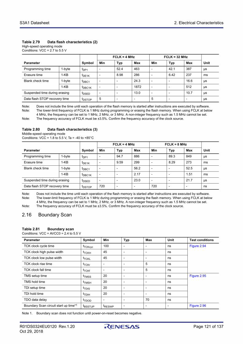
R01DS0324EU0120 Rev.1.20 Page 121 of 137Oct 29, 2018
S3A1 Datasheet 2. Electrical Characteristics
Note: Does not include the time until each operation of the flash memory is started after instructions are executed by software.Note: The lower-limit frequency of FCLK is 1 MHz during programming or erasing the flash memory. When using FCLK at below
4 MHz, the frequency can be set to 1 MHz, 2 MHz, or 3 MHz. A non-integer frequency such as 1.5 MHz cannot be set. Note: The frequency accuracy of FCLK must be ±3.5%. Confirm the frequency accuracy of the clock source.
Note: Does not include the time until each operation of the flash memory is started after instructions are executed by software.Note: The lower-limit frequency of FCLK is 1 MHz during programming or erasing the flash memory. When using FCLK at below
4 MHz, the frequency can be set to 1 MHz, 2 MHz, or 3 MHz. A non-integer frequency such as 1.5 MHz cannot be set.Note: The frequency accuracy of FCLK must be ±3.5%. Confirm the frequency accuracy of the clock source.
2.16 Boundary Scan
Note 1. Boundary scan does not function until power-on-reset becomes negative.
Table 2.79 Data flash characteristics (2)High-speed operating modeConditions: VCC = 2.7 to 5.5 V
Parameter Symbol
FCLK = 4 MHz FCLK = 32 MHz
UnitMin Typ Max Min Typ Max
Programming time 1-byte tDP1 - 52.4 463 - 42.1 387 μs
Erasure time 1-KB tDE1K - 8.98 286 - 6.42 237 ms
Blank check time 1-byte tDBC1 - - 24.3 - - 16.6 μs
1-KB tDBC1K - - 1872 - - 512 μs
Suspended time during erasing tDSED - - 13.0 - - 10.7 μs
Data flash STOP recovery time tDSTOP 5 - - 5 - - μs
Table 2.80 Data flash characteristics (3)Middle-speed operating modeConditions: VCC = 1.8 to 5.5 V, Ta = -40 to +85°C
Parameter Symbol
FCLK = 4 MHz FCLK = 8 MHz
UnitMin Typ Max Min Typ Max
Programming time 1-byte tDP1 - 94.7 886 - 89.3 849 μs
Erasure time 1-KB tDE1K - 9.59 299 - 8.29 273 ms
Blank check time 1-byte tDBC1 - - 56.2 - - 52.5 μs
1-KB tDBC1K - - 2.17 - - 1.51 ms
Suspended time during erasing tDSED - - 23.0 - - 21.7 μs
Data flash STOP recovery time tDSTOP 720 - - 720 - - ns
Table 2.81 Boundary scanConditions: VCC = AVCC0 = 2.4 to 5.5 V
Parameter Symbol Min Typ Max Unit Test conditions
TCK clock cycle time tTCKcyc 100 - - ns Figure 2.94
TCK clock high pulse width tTCKH 45 - - ns
TCK clock low pulse width tTCKL 45 - - ns
TCK clock rise time tTCKr - - 5 ns
TCK clock fall time tTCKf - - 5 ns
TMS setup time tTMSS 20 - - ns Figure 2.95
TMS hold time tTMSH 20 - - ns
TDI setup time tTDIS 20 - - ns
TDI hold time tTDIH 20 - - ns
TDO data delay tTDOD - - 70 ns
Boundary Scan circuit start up time*1 tBSSTUP tRESWP - - - Figure 2.96
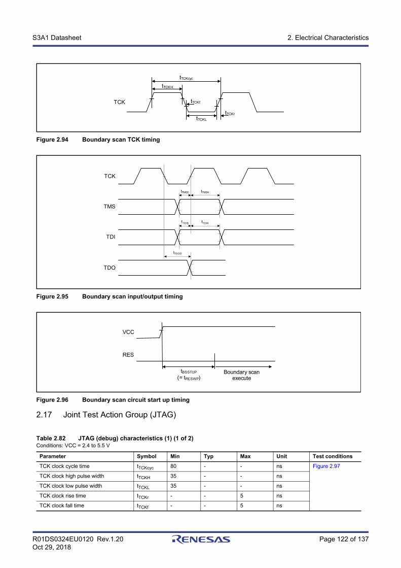
R01DS0324EU0120 Rev.1.20 Page 122 of 137Oct 29, 2018
S3A1 Datasheet 2. Electrical Characteristics
Figure 2.94 Boundary scan TCK timing
Figure 2.95 Boundary scan input/output timing
Figure 2.96 Boundary scan circuit start up timing
2.17 Joint Test Action Group (JTAG)
Table 2.82 JTAG (debug) characteristics (1) (1 of 2)Conditions: VCC = 2.4 to 5.5 V
Parameter Symbol Min Typ Max Unit Test conditions
TCK clock cycle time tTCKcyc 80 - - ns Figure 2.97
TCK clock high pulse width tTCKH 35 - - ns
TCK clock low pulse width tTCKL 35 - - ns
TCK clock rise time tTCKr - - 5 ns
TCK clock fall time tTCKf - - 5 ns
tTCKcyc
tTCKH
tTCKf
tTCKL
tTCKr
TCK
tTMSS tTMSH
tTDIS tTDIH
tTDOD
TCK
TMS
TDI
TDO
tBSSTUP
(= tRESWP)
VCC
RES
Boundary scan execute
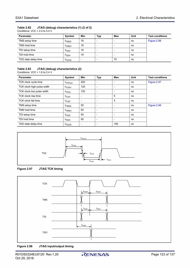
R01DS0324EU0120 Rev.1.20 Page 123 of 137Oct 29, 2018
S3A1 Datasheet 2. Electrical Characteristics
Figure 2.97 JTAG TCK timing
Figure 2.98 JTAG input/output timing
TMS setup time tTMSS 16 - - ns Figure 2.98
TMS hold time tTMSH 16 - - ns
TDI setup time tTDIS 16 - - ns
TDI hold time tTDIH 16 - - ns
TDO data delay time tTDOD - - 70 ns
Table 2.83 JTAG (debug) characteristics (2)Conditions: VCC = 1.6 to 2.4 V
Parameter Symbol Min Typ Max Unit Test conditions
TCK clock cycle time tTCKcyc 250 - - ns Figure 2.97
TCK clock high pulse width tTCKH 120 - - ns
TCK clock low pulse width tTCKL 120 - - ns
TCK clock rise time tTCKr - - 5 ns
TCK clock fall time tTCKf - - 5 ns
TMS setup time tTMSS 50 - - ns Figure 2.98
TMS hold time tTMSH 50 - - ns
TDI setup time tTDIS 50 - - ns
TDI hold time tTDIH 50 - - ns
TDO data delay time tTDOD - - 150 ns
Table 2.82 JTAG (debug) characteristics (1) (2 of 2)Conditions: VCC = 2.4 to 5.5 V
Parameter Symbol Min Typ Max Unit Test conditions
TCK
tTCKcyc
tTCKH
tTCKf
tTCKLtTCKr
TCK
TMS
TDI
TDO
tTMSS tTMSH
tTDIHtTDIS
tTDOD
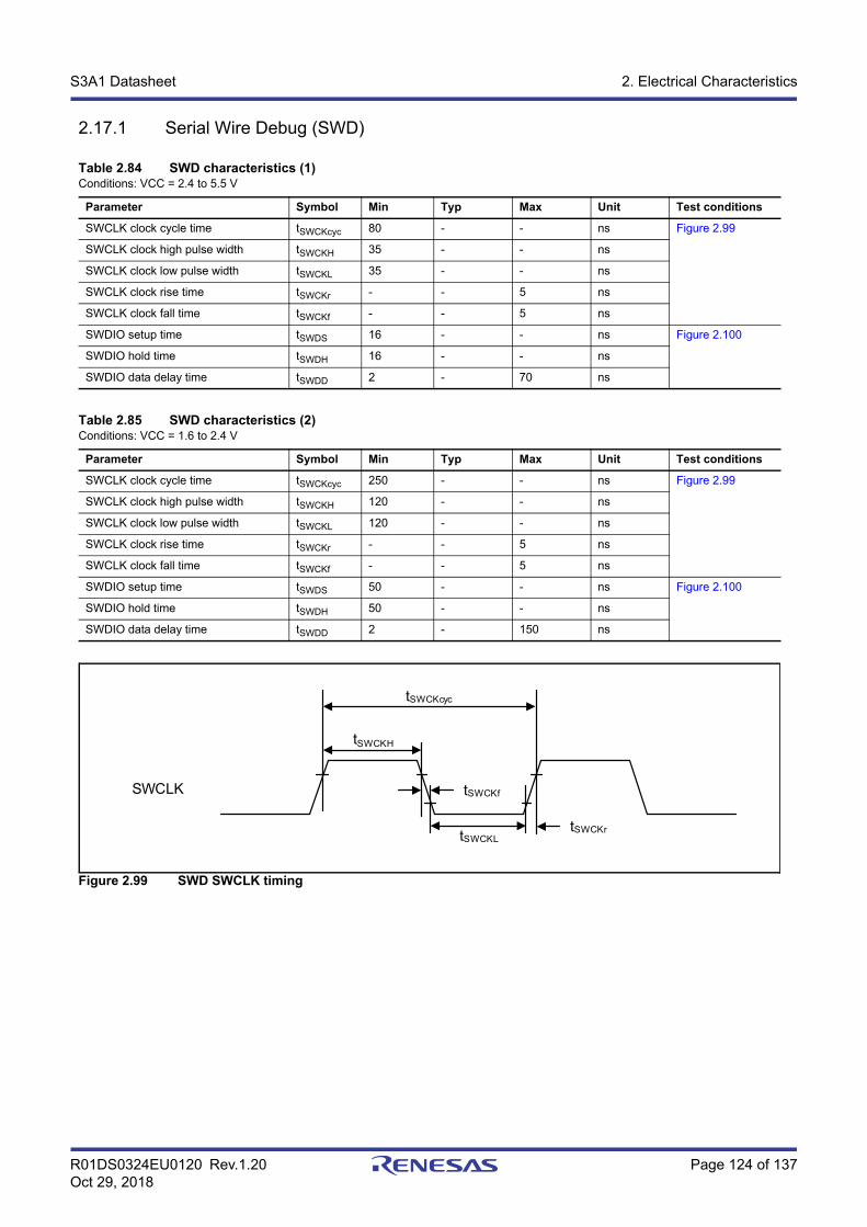
R01DS0324EU0120 Rev.1.20 Page 124 of 137Oct 29, 2018
S3A1 Datasheet 2. Electrical Characteristics
2.17.1 Serial Wire Debug (SWD)
Figure 2.99 SWD SWCLK timing
Table 2.84 SWD characteristics (1)Conditions: VCC = 2.4 to 5.5 V
Parameter Symbol Min Typ Max Unit Test conditions
SWCLK clock cycle time tSWCKcyc 80 - - ns Figure 2.99
SWCLK clock high pulse width tSWCKH 35 - - ns
SWCLK clock low pulse width tSWCKL 35 - - ns
SWCLK clock rise time tSWCKr - - 5 ns
SWCLK clock fall time tSWCKf - - 5 ns
SWDIO setup time tSWDS 16 - - ns Figure 2.100
SWDIO hold time tSWDH 16 - - ns
SWDIO data delay time tSWDD 2 - 70 ns
Table 2.85 SWD characteristics (2)Conditions: VCC = 1.6 to 2.4 V
Parameter Symbol Min Typ Max Unit Test conditions
SWCLK clock cycle time tSWCKcyc 250 - - ns Figure 2.99
SWCLK clock high pulse width tSWCKH 120 - - ns
SWCLK clock low pulse width tSWCKL 120 - - ns
SWCLK clock rise time tSWCKr - - 5 ns
SWCLK clock fall time tSWCKf - - 5 ns
SWDIO setup time tSWDS 50 - - ns Figure 2.100
SWDIO hold time tSWDH 50 - - ns
SWDIO data delay time tSWDD 2 - 150 ns
SWCLK
tSWCKcyc
tSWCKH
tSWCKf
tSWCKrtSWCKL
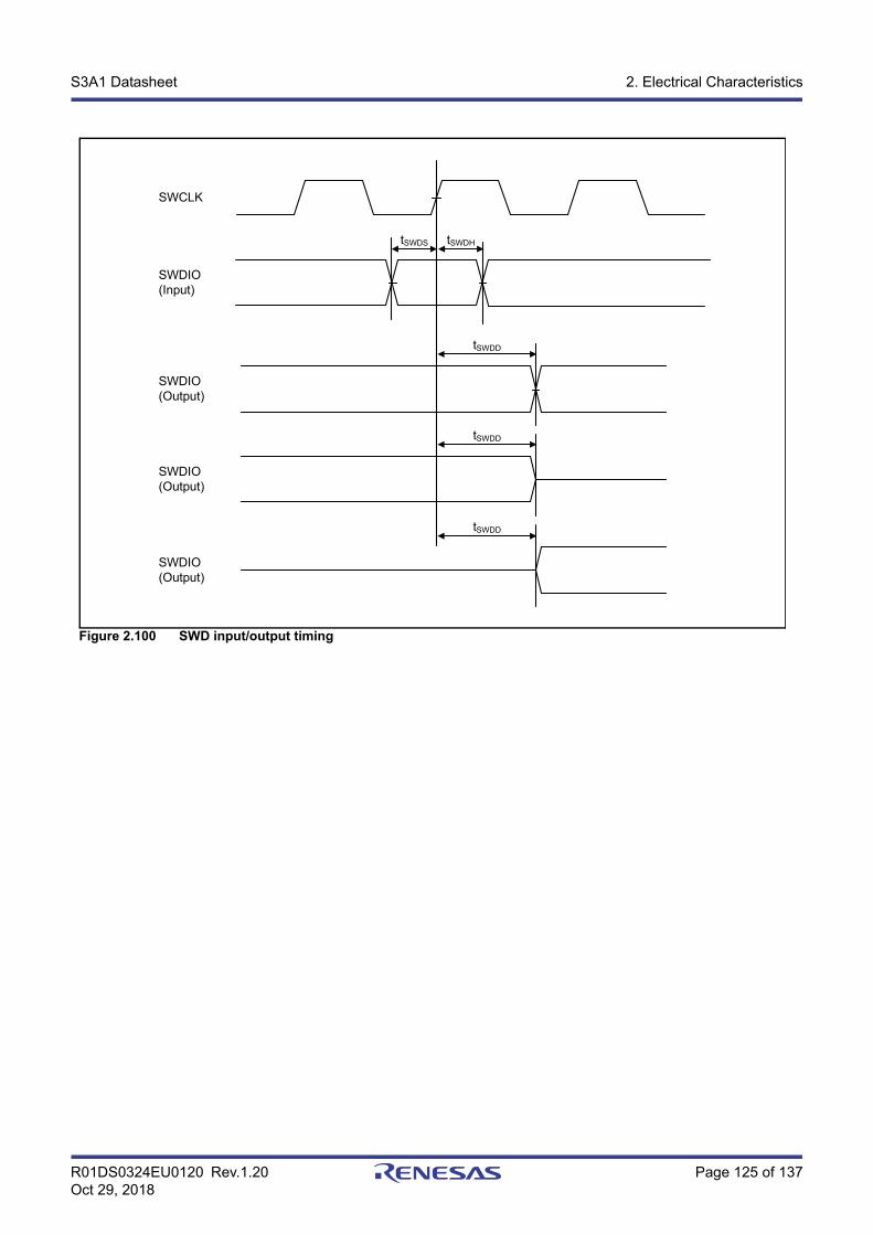
R01DS0324EU0120 Rev.1.20 Page 125 of 137Oct 29, 2018
S3A1 Datasheet 2. Electrical Characteristics
Figure 2.100 SWD input/output timing
SWDIO(Output)
SWDIO(Output)
SWDIO(Output)
tSWDD
tSWDD
tSWDD
SWCLK
SWDIO(Input)
tSWDS tSWDH
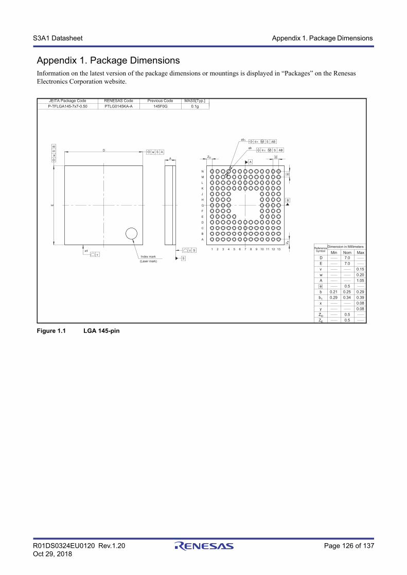
R01DS0324EU0120 Rev.1.20 Page 126 of 137Oct 29, 2018
S3A1 Datasheet Appendix 1. Package Dimensions
Appendix 1. Package DimensionsInformation on the latest version of the package dimensions or mountings is displayed in “Packages” on the Renesas Electronics Corporation website.
Figure 1.1 LGA 145-pin
0.5ZE
ZD 0.5
0.290.250.21b
b1
y 0.08
e 0.5
x
A 1.05
E 7.0
D 7.0
ReferenceSymbol
Dimension in Millimeters
Min Nom Max
0.29 0.34 0.39
0.08
w 0.20
v 0.15
PTLG0145KA-A 145F0GP-TFLGA145-7x7-0.50 0.1g
MASS[Typ.]RENESAS CodeJEITA Package Code Previous Code
131211109
N
M
L
K
J
Index mark
(Laser mark)
x4
v
AB
A
B
S
AB
S
S
y
S
87654321
B
C
D
E
F
G
H
A
S Aw S
wB
ZE
ZDA
e
e
E
D
φb1M
φb
φ
φ M
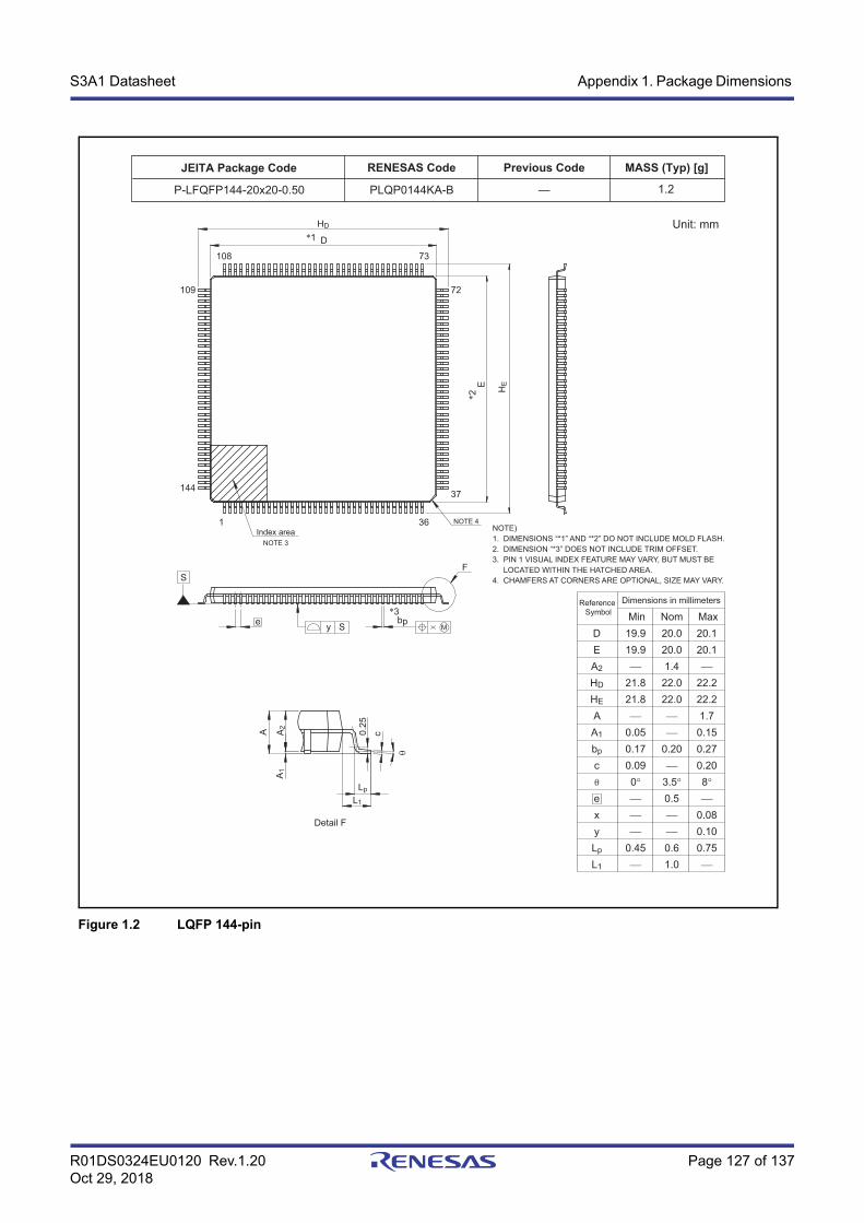
R01DS0324EU0120 Rev.1.20 Page 127 of 137Oct 29, 2018
S3A1 Datasheet Appendix 1. Package Dimensions
Figure 1.2 LQFP 144-pin
MASS (Typ) [g]
1.2
Unit: mm
Previous CodeRENESAS Code
PLQP0144KA-B —
JEITA Package Code
P-LFQFP144-20x20-0.50
DEA2
HD
HE
AA1
bp
c
exyLp
L1
19.919.9
21.821.8
0.050.170.090
0.45
Min NomDimensions in millimetersReference
Symbol Max20.020.01.422.022.0
0.20
3.50.5
0.61.0
20.120.1
22.222.21.7
0.150.270.208
0.080.100.75
NOTE)1. DIMENSIONS “*1” AND “*2” DO NOT INCLUDE MOLD FLASH.2. DIMENSION “*3” DOES NOT INCLUDE TRIM OFFSET.3. PIN 1 VISUAL INDEX FEATURE MAY VARY, BUT MUST BE LOCATED WITHIN THE HATCHED AREA.4. CHAMFERS AT CORNERS ARE OPTIONAL, SIZE MAY VARY.
HD
A2
A1
Lp
L1
Detail F
A c0.25
HE
D
E
108 73
72
37
109
144
1 36
F
NOTE 4
NOTE 3Index area
*1
*2
*3bpe y S
S
M
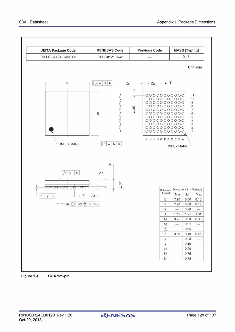
R01DS0324EU0120 Rev.1.20 Page 128 of 137Oct 29, 2018
S3A1 Datasheet Appendix 1. Package Dimensions
Figure 1.3 BGA 121-pin
MASS (Typ) [g]
0.15
Unit: mm
Previous CodeRENESAS Code
PLBG0121JA-A —
JEITA Package Code
P-LFBGA121-8x8-0.65
DEwAA1A2ebxyy1ZD
ZE
7.907.90—
1.110.25——
0.35—————
Min NomDimensions in millimetersReference
Symbol Max8.008.000.201.210.300.910.650.400.080.100.200.750.75
8.108.10—
1.310.35——
0.45—————
S
e
y1 S
A
A1
A2
Sy
Sxb A BM
Sw B
Sw A ZDZE
INDEX MARK
B
A
1234567891011
ABCDEFGHJKL
D
E
INDEX MARK
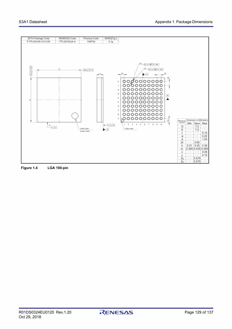
R01DS0324EU0120 Rev.1.20 Page 129 of 137Oct 29, 2018
S3A1 Datasheet Appendix 1. Package Dimensions
Figure 1.4 LGA 100-pin
P-TFLGA100-7x7-0.65 0.1g
MASS[Typ.]
100F0GPTLG0100JA-A
RENESAS CodeJEITA Package Code Previous Code
0.15v
0.20w
0.08
0.4850.4350.385
MaxNomMin
Dimension in MillimetersSymbol
Reference
7.0D
7.0E
1.05A
x
0.65e
0.10y
b1
b 0.31 0.35 0.39
0.575ZD
ZE 0.575
Index mark
Bw
Sw AS
A
H
G
F
E
D
C
B
1 2 3 4 5 6 7 8y S
S
A
v
×4
(Laser mark)
Index mark
J
K
9 10
D
E
e
e
A ZD
ZE
B
φ b
φ b1
φ× M S AB
φ× M S AB
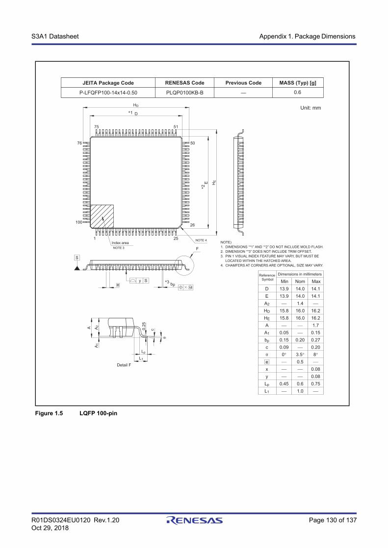
R01DS0324EU0120 Rev.1.20 Page 130 of 137Oct 29, 2018
S3A1 Datasheet Appendix 1. Package Dimensions
Figure 1.5 LQFP 100-pin
MASS (Typ) [g]
0.6
Unit: mm
Previous CodeRENESAS Code
PLQP0100KB-B —
JEITA Package Code
P-LFQFP100-14x14-0.50
DEA2
HD
HE
AA1
bp
c
exyLp
L1
13.913.9
15.815.8
0.050.150.090
0.45
Min NomDimensions in millimetersReference
Symbol Max14.014.01.4
16.016.0
0.20
3.50.5
0.61.0
14.114.1
16.216.21.7
0.150.270.208
0.080.080.75
NOTE)1. DIMENSIONS “*1” AND “*2” DO NOT INCLUDE MOLD FLASH.2. DIMENSION “*3” DOES NOT INCLUDE TRIM OFFSET.3. PIN 1 VISUAL INDEX FEATURE MAY VARY, BUT MUST BE LOCATED WITHIN THE HATCHED AREA.4. CHAMFERS AT CORNERS ARE OPTIONAL, SIZE MAY VARY.
HD
A2
A1
Lp
L1
Detail F
A c0.25
D
75
76
10026
251
50
51
F
NOTE 4
NOTE 3Index area
*1
HEE
*2
*3 bpey S
S
M
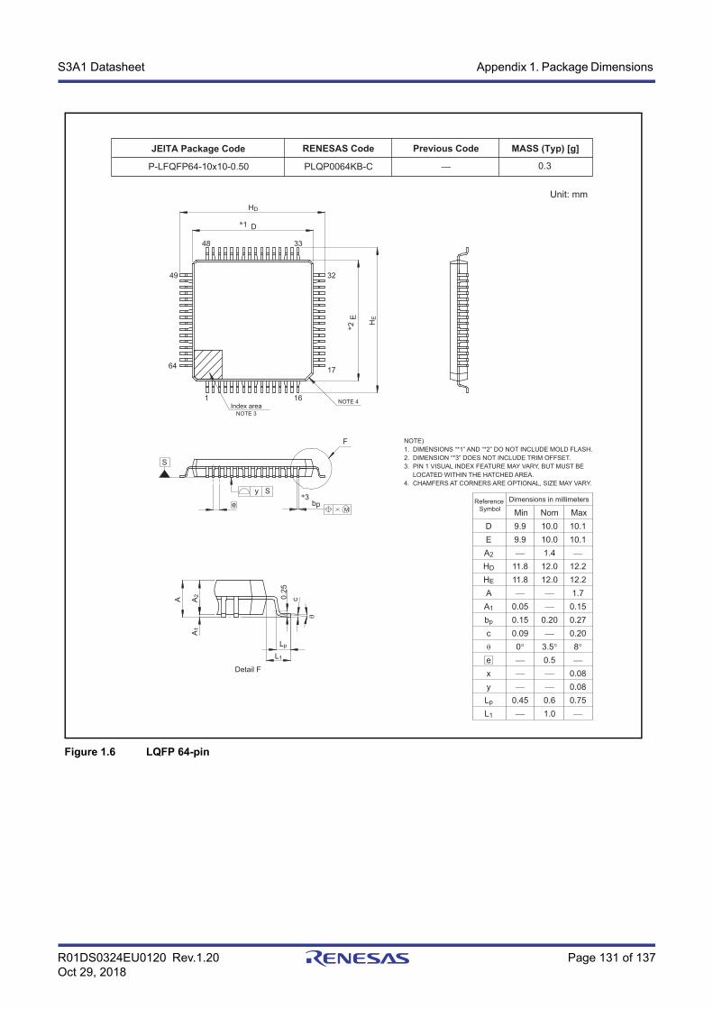
R01DS0324EU0120 Rev.1.20 Page 131 of 137Oct 29, 2018
S3A1 Datasheet Appendix 1. Package Dimensions
Figure 1.6 LQFP 64-pin
MASS (Typ) [g]
0.3
Unit: mm
Previous CodeRENESAS Code
PLQP0064KB-C —
JEITA Package Code
P-LFQFP64-10x10-0.50
DEA2
HD
HE
AA1
bp
c
exyLp
L1
9.99.9
11.811.8
0.050.150.090
0.45
Min NomDimensions in millimetersReference
Symbol Max10.010.01.412.012.0
0.20
3.50.5
0.61.0
10.110.1
12.212.21.70.150.270.208
0.080.080.75
NOTE)1. DIMENSIONS “*1” AND “*2” DO NOT INCLUDE MOLD FLASH.2. DIMENSION “*3” DOES NOT INCLUDE TRIM OFFSET.3. PIN 1 VISUAL INDEX FEATURE MAY VARY, BUT MUST BE LOCATED WITHIN THE HATCHED AREA.4. CHAMFERS AT CORNERS ARE OPTIONAL, SIZE MAY VARY.
HD
A2
A1
Lp
L1
Detail F
A c0.25
D
48 33
3249
17
161
64
F
NOTE 4
NOTE 3Index area
*1
HEE
*2
*3bpe
y S
S
M
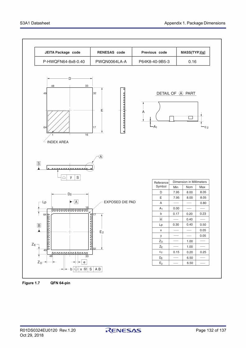
R01DS0324EU0120 Rev.1.20 Page 132 of 137Oct 29, 2018
S3A1 Datasheet Appendix 1. Package Dimensions
Figure 1.7 QFN 64-pin
Sy
e
Lp
Sxb A BM
A
D
E
48
32
33
16
17
1
64
A
S
B
A
D
E
49
DETAIL OF A PART
EXPOSED DIE PAD
JEITA Package code RENESAS code Previous code MASS(TYP.)[g]
P-HWQFN64-8x8-0.40 PWQN0064LA-A 0.16
161
17
3249
64
INDEX AREA
2
2
D
A
Lp
0.20
6.50
0.40
8.00
8.00
6.50
ReferanceSymbol Min Nom Max
Dimension in Millimeters
0.23
0.30 0.50
b 0.17
x
A 0.80
y 0.05
0.00
0.20
e
Z
Z
c
D
E
1
D
E
2
2
2
E
0.40
0.05
1.00
1.00
0.15 0.25
A1 c 2
8.057.95
8.057.95
Z
Z
D
E
3348
P64K8-40-9B5-3
S3A1 Microcontroller Group Datasheet
Website and SupportVisit the following vanity URLs to learn about key elements of the Synergy Platform, download components and relateddocumentation, and get support.
Proprietary NoticeAll text, graphics, photographs, trademarks, logos, artwork and computer code, collectively known as content, contained in this document is owned, controlled or licensed by or to Renesas, and is protected by trade dress, copyright, patent and trademark laws, and other intellectual property rights and unfair competition laws. Except as expressly provided herein, no part of this document or content may be copied, reproduced, republished, posted, publicly displayed, encoded, translated, transmitted or distributed in any other medium for publication or distribution or for any commercial enterprise, without prior written consent from Renesas.
Arm® and Cortex® are registered trademarks of Arm Limited. CoreSight™ is a trademark of Arm Limited.
CoreMark® is a registered trademark of the Embedded Microprocessor Benchmark Consortium.
Magic Packet™ is a trademark of Advanced Micro Devices, Inc.
SuperFlash® is a registered trademark of Silicon Storage Technology, Inc. in several countries including the United States and Japan.
Other brands and names mentioned in this document may be the trademarks or registered trademarks of their respectiveholders.
Rev. Date Summary
1.00 Oct 30, 2017 1st release
1.10 Mar 7, 2018 2nd release
1.20 Oct 29, 2018 3rd release
Synergy Software renesassynergy.com/software
Synergy Software Package renesassynergy.com/ssp
Software add-ons renesassynergy.com/addons
Software glossary renesassynergy.com/softwareglossary
Development tools renesassynergy.com/tools
Synergy Hardware renesassynergy.com/hardware
Microcontrollers renesassynergy.com/mcus
MCU glossary renesassynergy.com/mcuglossary
Parametric search renesassynergy.com/parametric
Kits renesassynergy.com/kits
Synergy Solutions Gallery renesassynergy.com/solutionsgallery
Partner projects renesassynergy.com/partnerprojects
Application projects renesassynergy.com/applicationprojects
Self-service support resources:
Documentation renesassynergy.com/docs
Knowledgebase renesassynergy.com/knowledgebase
Forums renesassynergy.com/forum
Training renesassynergy.com/training
Videos renesassynergy.com/videos
Chat and web ticket renesassynergy.com/support
Revision History

S3A1 Microcontroller Group Datasheet
Publication Date: Rev.1.20 Oct 29, 2018
Published by: Renesas Electronics Corporation
Colophon
Address ListGeneral Precautions
1. Precaution against Electrostatic Discharge (ESD) A strong electrical field, when exposed to a CMOS device, can cause destruction of the gate oxide and ultimately
degrade the device operation. Steps must be taken to stop the generation of static electricity as much as possible, and quickly dissipate it when it occurs. Environmental control must be adequate. When it is dry, a humidifier should be used. This is recommended to avoid using insulators that can easily build up static electricity. Semiconductor devices must be stored and transported in an anti-static container, static shielding bag or conductive material. All test and measurement tools including work benches and floors must be grounded. The operator must also be grounded using a wrist strap. Semiconductor devices must not be touched with bare hands. Similar precautions must be taken for printed circuit boards with mounted semiconductor devices.
2. Processing at power-on The state of the product is undefined at the time when power is supplied. The states of internal circuits in the LSI are
indeterminate and the states of register settings and pins are undefined at the time when power is supplied. In a finished product where the reset signal is applied to the external reset pin, the states of pins are not guaranteed from the time when power is supplied until the reset process is completed. In a similar way, the states of pins in a product that is reset by an on-chip power-on reset function are not guaranteed from the time when power is supplied until the power reaches the level at which resetting is specified.
3. Input of signal during power-off state Do not input signals or an I/O pull-up power supply while the device is powered off. The current injection that results
from input of such a signal or I/O pull-up power supply may cause malfunction and the abnormal current that passes in the device at this time may cause degradation of internal elements. Follow the guideline for input signal during power-off state as described in your product documentation.
4. Handling of unused pins Handle unused pins in accordance with the directions given under handling of unused pins in the manual. The input pins
of CMOS products are generally in the high-impedance state. In operation with an unused pin in the open-circuit state, extra electromagnetic noise is induced in the vicinity of the LSI, an associated shoot-through current flows internally, and malfunctions occur due to the false recognition of the pin state as an input signal become possible.
5. Clock signals After applying a reset, only release the reset line after the operating clock signal becomes stable. When switching the
clock signal during program execution, wait until the target clock signal is stabilized. When the clock signal is generated with an external resonator or from an external oscillator during a reset, ensure that the reset line is only released after full stabilization of the clock signal. Additionally, when switching to a clock signal produced with an external resonator or by an external oscillator while program execution is in progress, wait until the target clock signal is stable.
6. Voltage application waveform at input pin Waveform distortion due to input noise or a reflected wave may cause malfunction. If the input of the CMOS device
stays in the area between VIL (Max.) and VIH (Min.) due to noise, for example, the device may malfunction. Take care to prevent chattering noise from entering the device when the input level is fixed, and also in the transition period when the input level passes through the area between VIL (Max.) and VIH (Min.).
7. Prohibition of access to reserved addressesAccess to reserved addresses is prohibited. The reserved addresses are provided for possible future expansion of functions. Do not access these addresses as the correct operation of the LSI is not guaranteed.
8. Differences between products Before changing from one product to another, for example to a product with a different part number, confirm that the
change will not lead to problems. The characteristics of a microprocessing unit or microcontroller unit products in the same group but having a different part number might differ in terms of internal memory capacity, layout pattern, and other factors, which can affect the ranges of electrical characteristics, such as characteristic values, operating margins, immunity to noise, and amount of radiated noise. When changing to a product with a different part number, implement a system-evaluation test for the given product.
http://www.renesas.comSALES OFFICES
© 2018 Renesas Electronics Corporation. All rights reserved.
Colophon 7.2
(Rev.4.0-1 November 2017)
Notice1. Descriptions of circuits, software and other related information in this document are provided only to illustrate the operation of semiconductor products and application examples. You are fully responsible for
the incorporation or any other use of the circuits, software, and information in the design of your product or system. Renesas Electronics disclaims any and all liability for any losses and damages incurred by
you or third parties arising from the use of these circuits, software, or information.
2. Renesas Electronics hereby expressly disclaims any warranties against and liability for infringement or any other claims involving patents, copyrights, or other intellectual property rights of third parties, by or
arising from the use of Renesas Electronics products or technical information described in this document, including but not limited to, the product data, drawings, charts, programs, algorithms, and application
examples.
3. No license, express, implied or otherwise, is granted hereby under any patents, copyrights or other intellectual property rights of Renesas Electronics or others.
4. You shall not alter, modify, copy, or reverse engineer any Renesas Electronics product, whether in whole or in part. Renesas Electronics disclaims any and all liability for any losses or damages incurred by
you or third parties arising from such alteration, modification, copying or reverse engineering.
5. Renesas Electronics products are classified according to the following two quality grades: “Standard” and “High Quality”. The intended applications for each Renesas Electronics product depends on the
product’s quality grade, as indicated below.
"Standard": Computers; office equipment; communications equipment; test and measurement equipment; audio and visual equipment; home electronic appliances; machine tools; personal electronic
equipment; industrial robots; etc.
"High Quality": Transportation equipment (automobiles, trains, ships, etc.); traffic control (traffic lights); large-scale communication equipment; key financial terminal systems; safety control equipment; etc.
Unless expressly designated as a high reliability product or a product for harsh environments in a Renesas Electronics data sheet or other Renesas Electronics document, Renesas Electronics products are
not intended or authorized for use in products or systems that may pose a direct threat to human life or bodily injury (artificial life support devices or systems; surgical implantations; etc.), or may cause
serious property damage (space system; undersea repeaters; nuclear power control systems; aircraft control systems; key plant systems; military equipment; etc.). Renesas Electronics disclaims any and all
liability for any damages or losses incurred by you or any third parties arising from the use of any Renesas Electronics product that is inconsistent with any Renesas Electronics data sheet, user’s manual or
other Renesas Electronics document.
6. When using Renesas Electronics products, refer to the latest product information (data sheets, user’s manuals, application notes, “General Notes for Handling and Using Semiconductor Devices” in the
reliability handbook, etc.), and ensure that usage conditions are within the ranges specified by Renesas Electronics with respect to maximum ratings, operating power supply voltage range, heat dissipation
characteristics, installation, etc. Renesas Electronics disclaims any and all liability for any malfunctions, failure or accident arising out of the use of Renesas Electronics products outside of such specified
ranges.
7. Although Renesas Electronics endeavors to improve the quality and reliability of Renesas Electronics products, semiconductor products have specific characteristics, such as the occurrence of failure at a
certain rate and malfunctions under certain use conditions. Unless designated as a high reliability product or a product for harsh environments in a Renesas Electronics data sheet or other Renesas
Electronics document, Renesas Electronics products are not subject to radiation resistance design. You are responsible for implementing safety measures to guard against the possibility of bodily injury, injury
or damage caused by fire, and/or danger to the public in the event of a failure or malfunction of Renesas Electronics products, such as safety design for hardware and software, including but not limited to
redundancy, fire control and malfunction prevention, appropriate treatment for aging degradation or any other appropriate measures. Because the evaluation of microcomputer software alone is very difficult
and impractical, you are responsible for evaluating the safety of the final products or systems manufactured by you.
8. Please contact a Renesas Electronics sales office for details as to environmental matters such as the environmental compatibility of each Renesas Electronics product. You are responsible for carefully and
sufficiently investigating applicable laws and regulations that regulate the inclusion or use of controlled substances, including without limitation, the EU RoHS Directive, and using Renesas Electronics
products in compliance with all these applicable laws and regulations. Renesas Electronics disclaims any and all liability for damages or losses occurring as a result of your noncompliance with applicable
laws and regulations.
9. Renesas Electronics products and technologies shall not be used for or incorporated into any products or systems whose manufacture, use, or sale is prohibited under any applicable domestic or foreign laws
or regulations. You shall comply with any applicable export control laws and regulations promulgated and administered by the governments of any countries asserting jurisdiction over the parties or
transactions.
10. It is the responsibility of the buyer or distributor of Renesas Electronics products, or any other party who distributes, disposes of, or otherwise sells or transfers the product to a third party, to notify such third
party in advance of the contents and conditions set forth in this document.
11. This document shall not be reprinted, reproduced or duplicated in any form, in whole or in part, without prior written consent of Renesas Electronics.
12. Please contact a Renesas Electronics sales office if you have any questions regarding the information contained in this document or Renesas Electronics products.
(Note 1) “Renesas Electronics” as used in this document means Renesas Electronics Corporation and also includes its directly or indirectly controlled subsidiaries.
(Note 2) “Renesas Electronics product(s)” means any product developed or manufactured by or for Renesas Electronics.
Refer to "http://www.renesas.com/" for the latest and detailed information.
Renesas Electronics CorporationTOYOSU FORESIA, 3-2-24 Toyosu, Koto-ku, Tokyo 135-0061, JapanRenesas Electronics America Inc.1001 Murphy Ranch Road, Milpitas, CA 95035, U.S.A.Tel: +1-408-432-8888, Fax: +1-408-434-5351Renesas Electronics Canada Limited9251 Yonge Street, Suite 8309 Richmond Hill, Ontario Canada L4C 9T3Tel: +1-905-237-2004Renesas Electronics Europe LimitedDukes Meadow, Millboard Road, Bourne End, Buckinghamshire, SL8 5FH, U.KTel: +44-1628-651-700Renesas Electronics Europe GmbHArcadiastrasse 10, 40472 Düsseldorf, GermanyTel: +49-211-6503-0, Fax: +49-211-6503-1327Renesas Electronics (China) Co., Ltd.Room 1709 Quantum Plaza, No.27 ZhichunLu, Haidian District, Beijing, 100191 P. R. ChinaTel: +86-10-8235-1155, Fax: +86-10-8235-7679Renesas Electronics (Shanghai) Co., Ltd.Unit 301, Tower A, Central Towers, 555 Langao Road, Putuo District, Shanghai, 200333 P. R. ChinaTel: +86-21-2226-0888, Fax: +86-21-2226-0999Renesas Electronics Hong Kong LimitedUnit 1601-1611, 16/F., Tower 2, Grand Century Place, 193 Prince Edward Road West, Mongkok, Kowloon, Hong KongTel: +852-2265-6688, Fax: +852 2886-9022Renesas Electronics Taiwan Co., Ltd.13F, No. 363, Fu Shing North Road, Taipei 10543, TaiwanTel: +886-2-8175-9600, Fax: +886 2-8175-9670Renesas Electronics Singapore Pte. Ltd.80 Bendemeer Road, Unit #06-02 Hyflux Innovation Centre, Singapore 339949Tel: +65-6213-0200, Fax: +65-6213-0300Renesas Electronics Malaysia Sdn.Bhd.Unit 1207, Block B, Menara Amcorp, Amcorp Trade Centre, No. 18, Jln Persiaran Barat, 46050 Petaling Jaya, Selangor Darul Ehsan, MalaysiaTel: +60-3-7955-9390, Fax: +60-3-7955-9510Renesas Electronics India Pvt. Ltd.No.777C, 100 Feet Road, HAL 2nd Stage, Indiranagar, Bangalore 560 038, IndiaTel: +91-80-67208700, Fax: +91-80-67208777Renesas Electronics Korea Co., Ltd.17F, KAMCO Yangjae Tower, 262, Gangnam-daero, Gangnam-gu, Seoul, 06265 KoreaTel: +82-2-558-3737, Fax: +82-2-558-5338
Renesas Synergy™ PlatformS3A1 Microcontroller Group
R01DS0324EU0120
Back cover