Embed Size (px)
Citation preview

SALT, a 128-channel readout ASIC for Upstream Tracker in the LHCb Upgrade
Marek Idzikon behalf of LHCb UT working group
Faculty of Physics and Applied Computer ScienceAGH University of Science and Technology
TWEPP 2019 – Topical Workshop on Electronics for Particle Physics2 – 6 September 2019, Santiago de Compostela, Spain
M. Idzik, TWEEP 2019 2
Outline
• Introduction•SALT design
➢ Main blocks (FE, ADC, PLL, DLL, DSP)➢ SALTv3 versus previous versions
•SALT measurements➢ Analog test channels – scope measurements➢ SALT on hybrid with sensor type A – full tests
with transmission of digitized data
•Summary and plans

M. Idzik, TWEEP 2019 3
IntroductionUpgrade of LHCb Inner Tracker at LHC
• Upstream Tracker (UT) replaces the Tracker Turicensis (TT)
• 500 000 silicon strip detector channels
• Readout frequency increases to 40 MHz – currently Level-0 trigger output is limited to 1MHz
• New readout electronics is needed
LHCb detector
UT
M. Idzik, TWEEP 2019 4
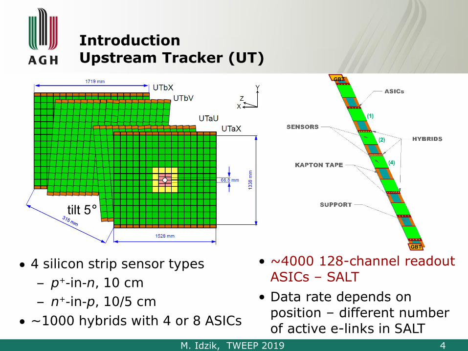
IntroductionUpstream Tracker (UT)
GBT
GBT
• 4 silicon strip sensor types
– p+-in-n, 10 cm
– n+-in-p, 10/5 cm
• ~1000 hybrids with 4 or 8 ASICs
• ~4000 128-channel readout ASICs – SALT
• Data rate depends on position – different number of active e-links in SALT
tilt 5°

M. Idzik, TWEEP 2019 5
IntroductionSALT specification
• CMOS 130 nm technology
• 128 channels, Front-end & ADC in each channel
• In/Out pitch 80/140um, No Top/Bottom pads (previous versions) SALTv3 uses it
• Sensor: capacitance 1.6–12 pF, AC coupled
• Both input signal polarities (p+-in-n and n+-in-p)
• Input charge range ~30ke–
• Noise: ENC ~1000e– @10pF + 50e–/pF
• Pulse shape: Tpeak ~25 ns, very short tail: ~5% after 2*Tpeak
• Crosstalk < 5%
• ADC: 6-bit resolution (5-bit&polarity), 40MS/s
• DSP functions: pedestal and common mode subtraction, zero-suppression
• Serialization & Data transmission: 320 Mbps e-links to GBT, SLVS I/O
• Slow control: I2C
• Power < 6 mW/channel
• Radiation hardness ~30 MRad

M. Idzik, TWEEP 2019 6
Outline
• Introduction•SALT design
➢ Main blocks (FE, ADC, PLL, DLL, DSP)➢ SALTv3 versus previous versions
•SALT measurements➢ Analog test channels – scope measurements➢ SALT on hybrid with sensor type A – full tests
with transmission of digitized data
•Summary and plans

M. Idzik, TWEEP 2019 7
SALT – Silicon ASIC for LHCb Tracking Architecture
• Front-end & ADC in each channel - 128 standard channels plus 2 test channels (nr -1,128 not shown) with analog outputs
• Digital Signal Processing (DSP) of the ADC data
• And many other features/blocks: PLL, DLL, TFC, I2C, serialiser, SLVS I/O, biasing DACs, monitoring ADCs, .... (not all shown)
• Only key functional blocks are discussed

M. Idzik, TWEEP 2019 8
SALT designPreamplifier&Shaper and Conv. Single-to-Diff.
Pream. Pole PZC + RealPole 2xComplexPoles 2xComplexPoles + RealPole 2xComplexZeros
Simplified circuit diagram
• 3-stage shaper (complex poles and zeros) gives the pulse with short tail
• Common mode (vcm_sh) at half power supply for both pulse polarities
• Single-to-Differential converter to generate differential signal for ADC
• Power consumption: ~1.5 mW
_
+_
+vcm_sh1
IN[i]
vcm_sh2
_
+
vcm_sh3
vcm_sh3Baseline DAC
vcm_s2d
adc_n[i] adc_p[i]
test[i]
Preamplifier + PZC Shaper Singletodifferential
Ctest

M. Idzik, TWEEP 2019 9
SALT design6-bit ADC
Main features: ● SAR architecture, 6-bit resolution● 40 MSps nominal sampling rate● Merge Capacitor Switching (MCS)● Capacitive DAC with 3b/2b split
● Dynamic comparator● Dynamic asynchronous logic● Bootstrapped input switches● Power consumption ~350µW
Update - dummy current option ON/OFF (const. current after conversion) added (additional ~400uW) to keep current consumption more stable

M. Idzik, TWEEP 2019 10
SALT designPLL, DLL
PLL
DLL
PLL features:
• High frequency (160 MHz) clock for DDR serializer
• Input frequency 40 MHz
• Power consumption ~0.5 mW @ 160 MHz
• 2 output phases (multiplexing) selected from 16 uniform phases (receiver synchronization)
DLL features:
• ADC sampling phase setting
• Test pulse phase setting
• Input frequency 40 MHz
• Power consumption ~0.7 mW
• 2 output phases (multiplexing) selected from 64 uniform phases
7bit DACdll_cp_curr
7bit DACdll_vcdl_curr
CLK Multiplexer
adc_clk
PD CPU
D
iCP
LPF VDLL
VCDL
iDLL
adc_clk_sel
ph0ph64
MAIN_CLK
2 x 64to1
dll_start
Out CLK Multiplexer2 x 2to1
dll_connect calib_clk_sel
calib_clk2
CT
dll_curr_ok
to voltage monitoring
HLD
dll_hld
dll_hld_debug
ph8 ph18 ph41
7bit DACpll_cp_curr 7bit DACpll_vco_curr
Clock Multiplexer
pll_out[0]
PFDMAIN_CLK(40MHz) CP
U
D
iCP
LPF VPLL
Multiphase VCO
iVC
O
2 x 16to1
pll_out[1]
pll_gain
pll_clk_sel[0]pll_clk_sel[1]
pll_clk[0] pll_clk[15]Clock Dividerby 4
pll_enable
pll_clk[1]
data_clk
to voltage monitoring
QDE
pll_connect

M. Idzik, TWEEP 2019 11
SALT designDSP operations
• Input data: 6 bits (5 bits plus sign)
• Noisy or dead channels can be masked
• All channel values can be inverted (1 config bit)
• Pedestal subtraction – subtraction in each channel
• CMS – (Mean) Common Mode Subtraction – sum of channels below CM threshold
– division by number of channels – average
– subtraction in each channel
• ZS – Zero suppression– only channels above ZS threshold are sent out
• PCK – Packet building
ChannelMasking
Pedestalsubtraction
CMS
ZeroSuppression
128 X 6b from ADC
Mem. & Ser.
Inversion
PCK
Analogue part Digital part (40 MHz) 160 MHzIN
FE ADCPed& MCM ZS PCK RAM IDL Ser
data_out
DLL PLLMAIN_CLK
da
ta_c
lk
ad
c_cl
k
Sync

M. Idzik, TWEEP 2019 12
• Measurements showed that SALTv2 did not fulfil specification:➢ main issue – 40MHz disturbance observed as baseline shift, when
sensor connected ● We have attributed the unsatisfactory SALTv2 performance mainly to large internal inductances (L) of power distribution lines and their couplings (amplifying the effects of large ADC current fluctuations)● These inductive effects were not seen in simulations of SALTv2 since design tools extract from the layout only R,C but not L● Contrary to previous SALT prototypes, SALTv3 was designed and simulated basing, NOT on layout-extracted chip, but on mix of schematic-extract with power distribution inductances added● List of main modifications in next slide...
SALT designSALTv3 versus SALTv2

M. Idzik, TWEEP 2019 13
● Single Channel➢ Analog front-end – highly improved PSRR➢ ADC - dummy current option added to minimize current fluctuations➢ Power supply domains separation optimized for inductive effects➢ Decoupling of analog supply removed to minimize LC factor
● Power distribution network➢ Analog front-end supplied from top&bottom pads (issue for 8-chip
hybrid), ➢ ADC supplied from digital domain mesh (output side)➢ Layout of analog power distribution drawn to minimize inductances
SALT designModifications of SALTv3 versus SALTv2

M. Idzik, TWEEP 2019 14
SALT DesignFloorplan and layout
4095um x 10900um
• Left & right sides bonded to the hybrid.
• Top&bottom pads for analog supply (issue for 8-chip hybrid) and wafer screening

M. Idzik, TWEEP 2019 15
Outline
• Introduction•SALT design
➢ Main blocks (FE, ADC, PLL, DLL, DSP)➢ SALTv3 versus previous versions
•SALT measurements➢ Analog test channels – scope measurements➢ SALT on hybrid with sensor type A – full tests
with transmission of digitized data
•Summary and plans

M. Idzik, TWEEP 2019 16
NOT Averaged
Measurements on analog test channelTransient response to MIP (~4fC) with 12pF external input capacitance
Averaged
Preamp
Preamp
S2Diff
S2Diff
For SALTv3 good pulse response is seen with large input capacitance.
With large input capacitance small 40MHz disturbance is still present (also in simulations)
M. Idzik, TWEEP 2019 17
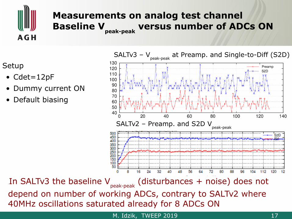
Measurements on analog test channelBaseline V
peak-peak versus number of ADCs ON
SALTv2 – Preamp. and S2D Vpeak-peak
SALTv3 – Vpeak-peak
at Preamp. and Single-to-Diff (S2D)
Setup
• Cdet=12pF
• Dummy current ON
• Default biasing
.In SALTv3 the baseline Vpeak-peak
(disturbances + noise) does not
depend on number of working ADCs, contrary to SALTv2 where 40MHz oscillations saturated already for 8 ADCs ON

M. Idzik, TWEEP 2019 18
Measurements on analog test channelSetup with “baby2” sensor
PCB with “baby2” sensor bonded to SALTv3
SALTv3
baby2 sensorCdet<2pF/strip

M. Idzik, TWEEP 2019 19
NOT Averaged
Measurements on analog test channelTransient response to MIP (~4fC)HV=200V, Dummy current ON
In SALTv3 good pulse response is observed with “baby2” sensor connected
Averaged
Preamp
Preamp
S2Diff
S2Diff
With “baby2” sensor connected 40MHz disturbance is practically NOT observed

M. Idzik, TWEEP 2019 20
Outline
• Introduction•SALT design
➢ Main blocks (FE, ADC, PLL, DLL, DSP)➢ SALTv3 versus previous versions
•SALT measurements➢ Analog test channels – scope measurements➢ SALT on hybrid with sensor type A – full tests
with transmission of digitized data
•Summary and plans

M. Idzik, TWEEP 2019 21
SALT on hybrid with sensor ASetup
Hybrid with the largest sensor and 4 SALT ASICs
SALT power consumption (@Vsup=1.2)• ~440mA (dummy
current OFF)• ~480mA (dummy
current ON)
sensor type A
~12pF/strip
biased @200V
ASIC 0
ASIC 1
ASIC 2
ASIC 3

M. Idzik, TWEEP 2019 22
SALT on hybrid with sensor ABaseline correction
Each channel is corrected by setting its own TrimDAC
TrimDAC scanfor ASIC 2
ASIC 2before correction
ASIC 2after correction
• Baseline correction works well
• Obtaining such data confirms that full processing chain (analog&digital) is functionally correct

M. Idzik, TWEEP 2019 23
SALT on hybrid with sensor type ANoise
Before TrimDAC correction After TrimDAC correction
ASIC 2 ASIC 2
• Various measurements showed noise rms slightly below 1 LSB
• SNR above 10 is estimated for MIP

M. Idzik, TWEEP 2019 24
SALT on hybrid with sensor ABaseline versus time
Before TrimDAC correction After TrimDAC correction
ASIC 2 ASIC 2
• In standard operation samples are taken every 25ns
• To obtain above plots internal DLL was scanned over all 64 phases (∆t=25ns/64) and data was averaged for each phase
• In standard operation small 40MHz component is seen as constant offset and can be subtracted

M. Idzik, TWEEP 2019 25
SALT on hybrid with sensor ABaseline versus time
After TrimDAC correction
ASIC 0
• In hybrid the worst 40MHz disturbance is seen in position “0”➢ Hybrid design (sensor biasing) is crucial for SALT performance
• In standard operation 40MHz disturbance is removed as offset

M. Idzik, TWEEP 2019 26
SALT on hybrid with sensor APulse shape
Before TrimDAC correction After TrimDAC correction
ASIC 2 ASIC 2
• Pulse shape is obtained via DLL scan
• Expected pulse shape is observed

M. Idzik, TWEEP 2019 27
Summary and plans
• The third SALT prototype was fabricated and tested. The tests confirmed that the measures taken against suspected inductive issues have proved effective
• Good results have been obtained for 4-chip hybrid. Full stave tests have been already started
• SALT production for 4-chip hybrids have been recently completed, wafer tests done, analysis of results ongoing
• For 8-chip hybrid a modified SALT version (without using top&bottom pads for power supply) is in fabrication. Will be checked a.s.a.p.
Thank you for attention

M. Idzik, TWEEP 2019 28
Backup

M. Idzik, TWEEP 2019 29
Measurements on analog test channelNoise, Pulse and ENC vs no. of ADCs ON
Satisfactory noise performance and good SNR (MIP pulse Cdet=12pF) observed with dummy current ON
Dummy current ON Dummy current OFF

M. Idzik, TWEEP 2019 30
SALTv2
In SALTv3 practically NO oscillations observed, contrary to SALTv2
Pulse shapes for bare chip are not shown since for each prototype nice pulses were observed without input capacitance
Bare chip, NO capacitanceVpp & baseline vs no. ADCs ON for chan. 128

M. Idzik, TWEEP 2019 31
NOT Averaged
Transient response to MIP (~4fC)Channel -1, C=24pF, Dummy current ON
Averaged
Preamp
Preamp
S2Diff
S2Diff
Good pulse response is seen even with 24pF external input capacitor
With 24pF external input capacitor 40MHz disturbance is still small


![ASIC/TRB Readout Status in Jülich - Indico [Home] · z-t ASIC/TRB Readout Status in Jülich Peter Wintz (IKP, FZ Jülich) STT RO WShop, Krakow, Jan-30/31 2016](https://img.pdfslide.net/doc/110x75/5e0a051f15f04325a03fce44/asictrb-readout-status-in-jlich-indico-home-z-t-asictrb-readout-status-in.jpg)


![Latest developments on the highly granular Silicon ... · SKIROC[14] (Silicon pin Kalorimeter Integrated ReadOut Chip) is the very front end ASIC designed for the readout of the Silicon](https://img.pdfslide.net/doc/110x75/5e314b7924ee241cf702c6fd/latest-developments-on-the-highly-granular-silicon-skiroc14-silicon-pin-kalorimeter.jpg)