Embed Size (px)
Citation preview


2
SAMSUNG ELECTRONICS RESERVES THE RIGHT TO CHANGE PRODUCTS, INFORMATION AND SPECIFICATIONS WITHOUT NOTICE.
Products and specifications discussed herein are for reference purposes only. All information discussed herein is provided on an "AS IS" basis,
without warranties of any kind. This document and all information discussed herein remain the sole and exclusive property of Samsung
Electronics. No license of any patent, copyright, mask work, trademark or any other intellectual property right is granted by one party to the
other party under this document, by implication, estoppel or other-wise. Samsung products are not intended for use in life support, critical
care, medical, safety equipment, or similar applications where product failure could result in loss of life or personal or physical harm, or any
military or defense application, or any governmental procurement to which special terms or provisions may apply. For updates or additional
information about Samsung products, contact your nearest Samsung office. All brand names, trademarks and registered trademarks belong to
their respective owners.

3
Table of Contents ................................................................................................................................................................... 3 List of Figures .......................................................................................................................................................................... 4 List of Tables ........................................................................................................................................................................... 4
Version History ...................................................................................................................................................................................... 5 Introduction ............................................................................................................................................................................ 6 ARTIK 020 Wireless starter Kit .............................................................................................................................................. 7
Description ............................................................................................................................................................................................ 7 Content................................................................................................................................................................................................... 7
ARTIK 020 WSTK Main Board ................................................................................................................................................ 8 ARTIK 020 Main Board Block Diagram ................................................................................................................................ 9 ARTIK 020 Main Board Connectors .................................................................................................................................... 10
Breakout Pads ..................................................................................................................................................................................... 10 Expansion Header ............................................................................................................................................................................... 11 Debug Connector (DBG) ..................................................................................................................................................................... 12 Simplicity Connector ........................................................................................................................................................................... 13
ARTIK 020 Main Board Debug Adapter ............................................................................................................................. 14 ARTIK 020 Main Board Power Supply and Reset ............................................................................................................. 15
Radio Board Power Selection ............................................................................................................................................................ 15 Board Controller Power ..................................................................................................................................................................... 15 ARTIK 020 Module Reset ..................................................................................................................................................................... 16 Battery Holder ..................................................................................................................................................................................... 16
ARTIK 020 Main Board Peripherals .................................................................................................................................... 17 Push Buttons and LEDs ...................................................................................................................................................................... 17 Memory LCD-TFT Display ................................................................................................................................................................... 17 Serial Flash .......................................................................................................................................................................................... 18 Relative Humidity and Temperature Sensor .................................................................................................................................... 18 Expansion Board ................................................................................................................................................................................. 19
Virtual COM Port .................................................................................................................................................................. 21 Board Controller ................................................................................................................................................................... 22 Advanced Energy Monitor ................................................................................................................................................... 23
Introduction ......................................................................................................................................................................................... 23 Advanced Energy Monitor - Theory of Operation ............................................................................................................................ 23 AEM Accuracy and Performance ....................................................................................................................................................... 24 Usage .................................................................................................................................................................................................... 24
Debugging ............................................................................................................................................................................. 25 Debug Modes....................................................................................................................................................................................... 25 Debugging during battery operation ................................................................................................................................................ 25
Ordering Information .......................................................................................................................................................... 26 Legal Information ................................................................................................................................................................. 27

4
Figure 1. ARTIK 020 Main Board ............................................................................................................................................. 6
Figure 2. ARTIK 020 Main Board ............................................................................................................................................. 8
Figure 3. ARTIK 020 Main Board Block Diagram .................................................................................................................. 9
Figure 4. Connector Placement on the ARTIK 020 Main Board ...................................................................................... 10
Figure 5. Pin out of the breakout Pad on the ARTIK 020 Main Board ............................................................................ 10
Figure 6. Expansion Header ................................................................................................................................................. 11
Figure 7. Debug Connector .................................................................................................................................................. 12
Figure 8. Simplicity Connector ............................................................................................................................................. 13
Figure 9. Mini Simplicity Connector .................................................................................................................................... 14
Figure 10. Power Switch Options ........................................................................................................................................ 15
Figure 11. Battery Holder Connection ................................................................................................................................ 16
Figure 12. ARTIK 020 Module 128x128 Pixel Memory LCD .............................................................................................. 17
Figure 13. ARTIK 020 Module Flash Connection ............................................................................................................... 18
Figure 14. Relative Humidity and Temperature Sensor ................................................................................................... 19
Figure 15. Available Sensors ................................................................................................................................................ 19
Figure 16. Virtual COM Port Interface ................................................................................................................................ 21
Figure 17. Advanced Energy Monitor ................................................................................................................................. 23
Table 1. ARTIK 020 WSTK Features ........................................................................................................................................ 6
Table 2. ARTIK 020 WSTK Package Content .......................................................................................................................... 7
Table 3. Expansion Header Pinout ...................................................................................................................................... 11
Table 4. Debug Connector Description .............................................................................................................................. 12
Table 5. Simplicity Connector Pin Description .................................................................................................................. 13
Table 6. Mini Simplicity Connector Pin Description .......................................................................................................... 14
Table 7. Virtual COM Port Interface Pins ............................................................................................................................ 21
Table 8. Debug Modes .......................................................................................................................................................... 25

5
Revision Date Description Maturity
1.0 10/12/2016 Initial Public Release Release

6
The ARTIK 020 Wireless Starter Kit (WSTK) is meant to help you evaluate the ARTIK 020 Module and get you started with your
own software development. This user guide helps you get an understanding on the most important components of the ARTIK
020 WSTK. The ARTIK 020 Module is based on Silicon Labs®
Wireless Gecko EFR32BG SoC and is using Silicon Labs®
Simplicity
Studio™ tools for development purposes.
Figure 1 shows a picture of the ARTIK 020 WSTK and Table 1 covers the various features.
Features Radio Board Software
Ethernet and USB connectivity ARTIK 020 Radio Board with 256kB Flash and
32kB RAM. Bluetooth® SDK
Advanced Energy Monitor Integrated high performance chip antenna Example applications
Virtual COM Port Transmit power up to 8 dBm iOS™ and Android™ applications
Packet Trace Interface support CPU core 32-bit ARM® Cortex®-M4
SEGGER J-Link on-board debugger
Debug Multiplexer supporting external hardware as
well as radio board
Relative Humidity and Temperature sensor
Ultra low power 128x128 pixel Memory LCD
User LEDs/Pushbuttons
20-pin 2.54 mm header for expansion boards
Breakout pads for direct access to all radio
Power sources include USB and CR2032 coin cell holder

7
The ARTIK 020 WSTK provides a complete development platform for the ARTIK 020 Module. The core of the Kit is the ARTIK
020 Main Board which features an on-board J-Link debugger, an Advanced Energy Monitor for real-time current and voltage
monitoring, a virtual COM port interface, and access to the Packet Trace Interface (PTI).
The ARTIK 020 Main Board is paired with a 8dBm ARTIK 020 Radio Board that plugs directly into the Main Board. The ARTIK
020 Radio Board features the ARTIK 020 Module itself and the RF interface. All debug functionality can also be used towards
an external target instead of the included Radio Board. To further enhance the WSTK usability, the WSTK Main Board contains
sensors and peripherals demonstrating some of the Wireless SoC's many capabilities.
Table 2 provides a list of components that are part of the ARTIK 020 Module Development Kit.
ARTIK 020 Module Development Kit
1x ARTIK 020 Main Board
1x ARTIK 020 Radio Board (with 8 dBm ARTIK 020 Module)
1x Expansion Board with buttons and sensor
1x Lithium battery
1x USB Type A <> USB Mini-B cables
1x Debug Adapter Board

8
Figure 2, shows the picture of the ARTIK 020 Main Board with its associated switches and indicators.

9
Figure 3 shows the block diagram of the ARTIK 020 Main Board.

10
Figure 4 shows the placement of the various connectors that are present on the ARTIK 020 Main Board.
Most of the ARTIK 020 Module pins are routed from the radio board to breakout pads at the top and bottom edges of the
ARTIK 020 Main Board. A 2.54 mm pitch pin header can be soldered on for easy access to the pins. Figure 5 shows you how
the pins of the ARTIK 020 Module are mapped onto the pin numbers printed on the breakout pads. To see the available
functions on each, please refer to the ARTIK 020 Module Data Sheet.

11
On the right hand side of the board an angled 20 pin expansion header is provided to allow connection of peripherals or
plugin boards. The connector contains a number of I/O pins that can be used with most of the ARTIK 020 Module features.
Additionally, the VMCU, 3V3 and 5V power rails are also exported. The connector follows a standard which ensures that
commonly used peripherals such as an SPI, a UART and an I2C bus are available on fixed locations in the connector. The rest
of the pins are used for general purpose IO. Figure 6 shows the pin assignment of the expansion header. Because of
limitations in the number of available GPIO pins, some of the expansion header pins are shared between features.
The pin-routing on the ARTIK 020 Module is very flexible, so most peripherals can be routed to any pin. However, many pins
are shared between the Expansion Header and other functions on the Main Board. Table 3 includes an overview of the Main
Board features that share pins with the Expansion Header.
Pin Connection Expansion Header Function Main Board Function/ Feature Peripheral Mapping
4 PC6 SPI_MOSI DISP_MOSI USART1_TX #11
6 PC7 SPI_MISO USART1_RX #11
8 PC8 SPI_SCLK DISP_SCLK USART1_CLK #11
10 PC9 SPI_CS USART1_CS #11
12 PA0 UART_TX VCOM_TX USART0_TX #0
14 PA1 UART_RX VCOM_RX USART0_RX #0
16 PC10 I2C_SDA SENSOR_I2C_SDA I2C0_SDA #15
3 PA2 UART_CTS VCOM_CTS USART0_CLK #0
5 PA3 UART_RTS VCOM_RTS USART0_CS #0
7 PF4 GPIO
9 PF5 GPIO
11 PB11 GPIO PTI_CLK
13 PF3 GPIO DBG_TDI
15 PC11 I2C_SCL SENSOR_I2C_SCL I2C0_SCL #15
*Please note that pin PF3 is used for DBG_TDI in JTAG mode only. When Serial Wire Debugging is used, PF3 can be used for other purposes.

12
The Debug Connector serves a dual purpose. Based on the "debug mode", that can be selected using Silicon Labs®
Simplicity
Studio™
. In the "Debug IN" mode this connector allows an external debug emulator to be used with the on-board ARTIK 020
Module. In the "Debug OUT" mode this connector allows the kit to be used as a debugger towards an external target. In the
"Debug MCU" (default) mode this connector is isolated from the debug interface of both the Board Controller and the on-
board target device. Because this connector is automatically switched to support the different operating modes, it is only
available when the Board Controller is powered (J-Link USB cable connected). If debug access to the target device is required
when the Board Controller is unpowered, this should be done by connecting directly to the appropriate breakout pins. The
pinout of the connector follows that of the standard ARM Cortex Debug+ETM 19-pin connector. The pinout is described in
detail below.
Note that the pin-out matches the pin-out of an ARM Cortex Debug+ETM connector, but these are not fully compatible as pin
7 is physically removed from the Cortex Debug+ETM connector. Some cables have, a small plug that prevent them from being
used when this pin is present. If this is the case, remove the plug, or use a standard 2x10 1.27 mm straight cable instead. For
more information of the debug functionality using Silicon Labs®
Simplicity Studio™,
see the Debugging section.
Pin Function Note
1 VTARGET Target voltage on the debugged application
2 TMS / SDWIO / C2D JTAG test mode select, Serial Wire data or C2 data
4 TCK / SWCLK / C2CK JTAG test clock, Serial Wire clock or C2 clock
6 TDO/SWO JTAG test data out or Serial Wire Output
8 TDI / C2Dps JTAG test data in, or C2D "pin sharing" function
10 RESET / C2CKps Target device reset, or C2CK "pin sharing" function
12 TRACECLK ETM Trace Clock
14 TRACED0 ETM Trace Data 0
16 TRACED1 ETM Trace Data 1
18 TRACED2 ETM Trace Data 2
20 TRACED3 ETM Trace Data 3
9 Cable detect This signal must be pulled to ground by the external debugger or application for cable insertion
detection.
11,13 NC Not Connected
3,5,15,17,19 GND Ground

13
The Simplicity Connector featured on the board enables advanced debugging features such as the Advanced Energy Monitor
(AEM), the Virtual COM port and the Packet Trace Interface to be used towards an external target. The pinout is illustrated in
Figure 8 whereas the pin description is covered in Table 5.
As an example when AEM is used, the current drawn from the VMCU voltage pin is included in the AEM measurements, while
the 3V3 and 5V voltage pins are not. To monitor the current consumption of an external target with the AEM, unplug the
ARTIK 020 Module from the Main Board to avoid that current consumption is added to the measurements.
Pin Function Note
1 VMCU 3.3 V power rail, monitored by the AEM
3 3 3V3 3.3 V power rail 3.3 V power rail
5 5 5V 5 V power rail 5 V power rail
2 2 VCOM_TX_MOSI Virtual COM Tx/MOSI Virtual COM Tx/MOSI
4 4 VCOM_RX_MISO Virtual COM Rx/MISO Virtual COM Rx/MISO
6 6 VCOM_CTS_#SCLK Virtual COM CTS/SCLK Virtual COM CTS/SCLK
8 VCOM_#RTS_#CS Virtual COM RTS/CS
10 PTI0_SYNC Packet Trace 0 Sync
13 PTI0_DATA Packet Trace 0 Data
14 PTI0_CLK Packet Trace 0 Clock
26 PTI1_SYNC Packet Trace 1 Sync
18 PTI1_DATA Packet Trace 1 Data
20 PTI1_CLK Packet Trace 1 Clock
17 EXT_ID_SCL Board ID SCL
19 EXT_ID_SDA Board ID SDA
7,9,11,13,15 GND Ground

14
Included with the ARTIK 020 Main Board is one Debug Adapter Board. This board is an adapter which plugs directly into the
Debug Connector and the Simplicity Connector on the mainboard. It combines selected functionality to a smaller footprint
10-pin connector, which is more suitable for space constrained designs. For versatility, the Debug Adapter features three
different 10-pin debug connectors:
- Silicon Labs®
Mini Simplicity Connector
- ARM Cortex 10-pin Debug Connector
- Silicon Labs®
ISA3 Packet Trace
The ARM Cortex 10-pin Debug Connector follows the standard Cortex pin-out defined by ARM and allows the Starter Kit to
be used to debug hardware designs that use this connector.
The ISA3 connector follows the same pin-out as the Packet Trace connector found on the Silicon Labs®
Ember Debug
Adapter (ISA3). This allows the Starter Kit to be used to debug hardware designs that use this connector.
The Mini Simplicity Connector is designed to offer advanced debug features from the ARTIK 020 Main Board on a 10-pin
connector:
- Serial Wire Debug (SWD) with SWO
- Packet Trace Interface (PTI)
- Virtual COM Port (VCOM)
- AEM Monitored voltage rail
Note: Packet Trace is only available on Wireless STK Main Boards. MCU Starter Kits do not support Packet Trace.
Pin Function Description
1 VAEM Target voltage on the debugged application. Supplied and monitored by the AEM when power
selection switch is in the "AEM" position.
2 GND Ground
3 RST Reset
4 VCOM_RX Virtual COM Rx
5 VCOM_TX Virtual COM Tx
6 SWO Serial Wire Output
7 SWDIO Serial Wire Data
8 SWCLK Serial Wire Clock
9 PTI_FRAME Packet Trace Frame Signal
10 PTI_DATA Packet Trace Data Signal

15
The ARTIK 020 Module can be powered by one of these sources:
1. The debug USB cable
2. A 3V coin cell battery
3. USB regulator on the Radio Board (for devices with USB support only).
The power source for radio board is selected with the slide switch in the lower left corner of the Wireless STK board. shows
how the different power sources can be selected with the slide switch.
With the switch in the AEM position, a low noise 3.3 V LDO on the ARTIK 020 Main Board is used to power the Radio board.
This LDO is again powered from the debug USB cable. The Advanced Energy Monitor is now also connected in series, allowing
accurate high speed current measurements and energy debugging/profiling.
With the switch in the USB position, radio boards with USB-support can be powered by a regulator on the radio board itself.
BRD4151A does not contain an USB regulator, and setting the switch in the USB position will cause the ARTIK 020 Module to
be unpowered.
Finally, with the switch in the BAT position, a 20 mm coin cell battery in the CR2032 socket can be used to power the device.
With the switch in this position no current measurements are active. This is the recommended switch position when
powering the radio board with an external power source.
Note: Please be aware that the current sourcing capabilities of a coin cell battery might be too low to supply certain wireless
applications.
Note: The Advanced Energy Monitor can only measure the current consumption of the ARTIK 020 Module when the power
selection switch is in the AEM position.
The board controller is responsible for important features such as the debugger and the Advanced Energy Monitor, and is
powered exclusively through the USB port in the top left corner of the board. This part of the ARTIK 020 Development Kit
resides on a separate power domain, so a different power source can be selected for the target device while retaining
debugging functionality. This power domain is also isolated to prevent current leakage from the target power domain when
power to the Board Controller is removed. The board controller power domain is exclusively supplied by the J-Link USB cable,

16
and is not influenced by the position of the power switch. The kit has been carefully designed to keep the board controller
and the target power domains isolated from each other as one of them powers down. This ensures that the ARTIK 020
Module will continue to operate in the USB and BAT modes.
The ARTIK 020 Module can be reset by a few different sources:
1. A user pressing the RESET button
2. The on-board debugger pulling the #RESET pin low
3. An external debugger pulling the #RESET pin low
In addition to the reset sources mentioned above, the Board Controller will also issue a reset to the ARTIK 020 Module when
booting up. This means that removing power to the Board Controller (plugging out the J-Link USB cable) will not generate a
reset, but plugging the cable back in will, as the Board Controller boots up.
In radio applications with high output power, peak current consumption will exceed the current sourcing capacity of a coin-
cell battery. To support evaluation of the ARTIK 020 Module in situations where powering the kit from a wired USB
connection is impractical, for instance during range-tests, the kit is supplied with a battery holder for 2 AA batteries.
To use the battery holder, first set the power switch in the BAT position. Then attach the cable to pin 1 and 2 on the
expansion header, orienting the connector so the black cable goes down towards pin 1, and the red cable up towards pin 2.
Figure 11 explains the situation.
Warning: There is no reverse voltage protection on the VMCU pin! Ensure that the battery holder is connected the right way.
Failure to do so may result in damage to the radio board and its components.

17
The ARTIK 020 Main Board has a set of peripherals that showcase some of the features of the ARTIK 020 Module. Be aware
that most ARTIK 020 Module I/O routed to peripherals are also routed to the breakout pads. This must be taken into
consideration when using the breakout pads for your application.
The ARTIK 020 Main Board has two user push buttons marked PB0 and PB1. They are connected directly to the ARTIK 020
Module, and are de-bounced by RC filters with a time constant of 1ms. The buttons are connected to pins PF6 and PF7. The
ARTIK 020 Main Board also features two yellow LEDs marked LED0 and LED1 that are controlled by GPIO pins on the ARTIK
020 Module. The LEDs are connected to pins PF4 and PF5 in an active-high configuration.
A 1.28-inch SHARP Memory LCD-TFT is available on the kit to enable interactive applications to be developed. The display has
a high resolution of 128 by 128 pixels, and consumes very little power. It is a reflective monochrome display, so each pixel
can only be light or dark, and no backlight is needed in normal daylight conditions. Data sent to the display is stored in the
pixels on the glass, which means no continuous refreshing is required to maintain a static image. The display interface
consists of an SPI-compatible serial interface and some extra control signals. Pixels are not individually addressable, instead
data is sent to the display one line (128 bits) at a time. The Memory LCD-TFT display is shared with the kit Board Controller,
allowing the Board Controller application to display useful information when the user application is not using the display. The
user application always controls ownership of the display with the DISP_ENABLE line:
- 0: The Board Controller has control of the display
- 1: The user application ARTIK 020 Module has control of the display
Power to the display is sourced from the target application power domain when the ARTIK 020 Module controls the display,
and from the Board Controller's power domain when the DISP_ENABLE line is low. Data is clocked in on DISP_MOSI when
DISP_CS is high, and the clock is sent on DISP_SCLK. The maximum supported clock speed is 1.1MHz. DISP_COM is the "COM
Inversion" line. It must be pulsed periodically to prevent static build-up in the display itself. Please refer to the display
application information for details on driving the display: (http://www.sharpmemorylcd.com/1-28-inch-memory-lcd.html).
18
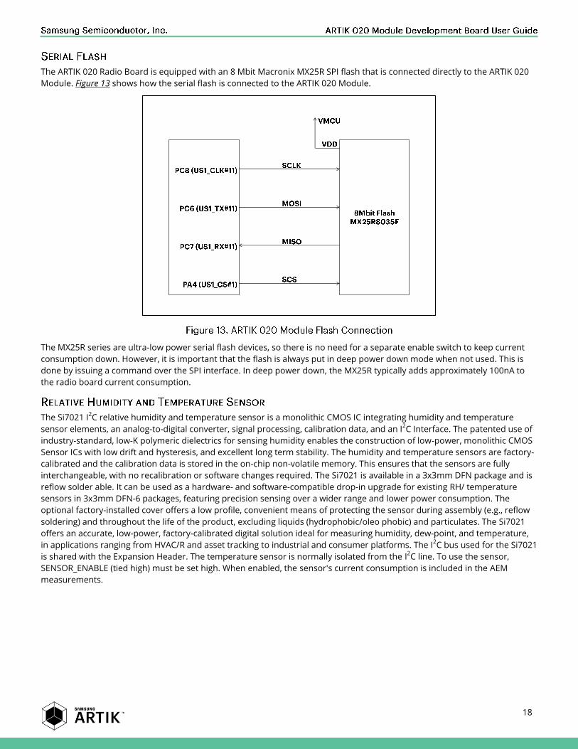
The ARTIK 020 Radio Board is equipped with an 8 Mbit Macronix MX25R SPI flash that is connected directly to the ARTIK 020
Module. Figure 13 shows how the serial flash is connected to the ARTIK 020 Module.
The MX25R series are ultra-low power serial flash devices, so there is no need for a separate enable switch to keep current
consumption down. However, it is important that the flash is always put in deep power down mode when not used. This is
done by issuing a command over the SPI interface. In deep power down, the MX25R typically adds approximately 100nA to
the radio board current consumption.
The Si7021 I2C relative humidity and temperature sensor is a monolithic CMOS IC integrating humidity and temperature
sensor elements, an analog-to-digital converter, signal processing, calibration data, and an I2C Interface. The patented use of
industry-standard, low-K polymeric dielectrics for sensing humidity enables the construction of low-power, monolithic CMOS
Sensor ICs with low drift and hysteresis, and excellent long term stability. The humidity and temperature sensors are factory-
calibrated and the calibration data is stored in the on-chip non-volatile memory. This ensures that the sensors are fully
interchangeable, with no recalibration or software changes required. The Si7021 is available in a 3x3mm DFN package and is
reflow solder able. It can be used as a hardware- and software-compatible drop-in upgrade for existing RH/ temperature
sensors in 3x3mm DFN-6 packages, featuring precision sensing over a wider range and lower power consumption. The
optional factory-installed cover offers a low profile, convenient means of protecting the sensor during assembly (e.g., reflow
soldering) and throughout the life of the product, excluding liquids (hydrophobic/oleo phobic) and particulates. The Si7021
offers an accurate, low-power, factory-calibrated digital solution ideal for measuring humidity, dew-point, and temperature,
in applications ranging from HVAC/R and asset tracking to industrial and consumer platforms. The I2C bus used for the Si7021
is shared with the Expansion Header. The temperature sensor is normally isolated from the I2C line. To use the sensor,
SENSOR_ENABLE (tied high) must be set high. When enabled, the sensor's current consumption is included in the AEM
measurements.

19
The Expansion Board included with the WSTK includes the following features:
- 1x 3-axis accelerometer (Bosch Sensortech BMA280)
- 1x Joystick with 9 measureable positions
- 2x Push button and 2x LEDs sharing the same I/O pins
The connections between the Expansion Board and the ARTIK 020 Module are shown in Figure 15.
The subsequent sections contain more detailed information about each feature.
The Expansion Board contains a Bosch Sensortec BMA280 triaxial, low-power, low-g accelerometer sensor with SPI
interface. It features 14-bit digital resolution and allows very low-noise measurement of acceleration in 3 perpendicular axes
and can therefore sense tilt, motion, shock and vibration.
For more details on the Bosch Sensortec BMA280 please visit http://www.boschsensortec.com/bst/products/
all_products/bma280

20
The Expansion Board contains two push buttons (marked BTN2 and BTN3 on the PCB) and two LEDs (LED2 and LED3 not
marked but placed correspondingly above the push button markings correspondingly). The push buttons and LEDs share the
same two module I/O pins. Each push button is connected to a LED through a transistor, allowing both I/O's to be used
either as an input (for reading the push button state) or as an output (to control the LED state on or off).
When configured as an input, "0" indicates that the button is being pressed and "1" that the push button is not being pressed.
Likewise, when configured as an output, "0" will turn the LED on and "1" will turn it off.
Pressing a push button will also light up the corresponding LED because the LED is controlled by the same line (state)
regardless of whether it is the Module or the push button that pulls the line low.
The push buttons are de-bounced by RC filters with a time constant of about 1ms. Pressing the push button while having the
pin configured as an output in high state ("1") will not cause damage, but will cause extra current to flow.
The WSTK has an analog joystick with 9 measureable positions. This joystick is connected to the ARTIK 020 Module pin PD4
and uses different resistor values to create voltages measurable by the internal ADC on the BGM111 Module. The joystick
output is connected to AD Channel 0 (ADC0). The figure below shows the connection between the joystick and the ARTIK 020
Module.

21
When enabling virtual serial communication (VCOM), the board controller makes communication possible on the following
interfaces:
1. Virtual USB COM port using a CDC driver
2. TCP/IP, by connecting to the WSTK on port 4901 with a telnet client
The VCOM functionality can operate in two different modes:
1. Transparent mode allows the target to communicate using a regular serial driver. The board controller forwards the
raw byte stream to its interfaces.
2. BSP-mode is initiated by a BSP call in the target application. This mode enables the target to use all BSP functionality,
while having access to VCOM over USB and Ethernet.
The Virtual COM port consists of a physical UART between the target device and the board controller see Figure 16, and a
logical function in the board controller that makes the serial port available to the host PC over USB or Ethernet. The UART
interface consists of four pins and an enable signal. Details of the UART Interface are given in Table 7.
Signal Description
VCOM_TX Transmit data from the ARTIK 020 Module to the board controller
VCOM_RX Receive data from the board controller to the ARTIK 020 Module
VCOM_CTS Clear to Send hardware flow control input, asserted by the board controller when it is ready to receive more data
VCOM_RTS Request to Send hardware flow control output, asserted by the ARTIK 020 Module when it is ready to receive more data
VCOM_ENABLE Enables the VCOM interface, allowing data to pass through to the board controller

22
The ARTIK 020 Main Board contains a board controller that is responsible for performing various board-level tasks, such as
handling the debugger and the Advanced Energy Monitor. An interface is provided between the ARTIK 020 Module and the
board controller in the form of a UART connection. The connection is enabled by setting the VCOM_ENABLE (PA5) line high,
and using the lines VCOM_TX (PA0) and VCOM_RX (PA1) for communication.
Specific library functions have been provided in the ARTIK 020 Module Main Board BSP that support various requests to be
made to the board controller, such as querying AEM voltage or current.
Note: The board controller is only available when USB power is connected.

23
Any embedded developer seeking to make his embedded code spend as little energy as the underlying architecture supports,
needs tools to easily and quickly discover inefficiencies in the running application. This is what the Simplicity Studio™
Energy
Profiler is designed to do. It will in real-time graph and log current as a function of time while correlating this to the actual
target application code running on the ARTIK 020 Module. There are multiple features in the profiler software that allows for
easy analysis, such as markers and statistics on selected regions of the current graph or aggregate energy usage by different
parts of the application.
The AEM circuitry on the board is capable of measuring current signals in the range of 0.1μA to 95mA, which is a dynamic
range of almost 120dB. It can do this while maintaining approximately 10kHz of current signal bandwidth. This is
accomplished through a combination of a highly capable current sense amplifier, multiple gain stages and signal processing
within the kit's board controller before the current sense signal is read by a host computer for display and/or storage.
The current sense amplifier measures the voltage drop over a small series resistor, and the gain stage further amplifies this
voltage with two different gain settings to obtain two current ranges. The transition between these two ranges occurs around
250μA. The current signal is combined with the target processor's Program Counter (PC) sampling by utilizing a feature of the
ARM CoreSight debug architecture. The ITM (Instrumentation Trace Macrocell) block can be programmed to sample the
MCU's PC at periodic intervals (50kHz) and output these over SWO pin ARM devices. When these two data streams are fused
and correlated with the running application's memory map, an accurate statistical profile can be built over time, that shows
the energy profile of the running application in real-time.
At power-up or on a power-cycle, an automatic AEM calibration is performed. This calibration compensates for any offset
errors in the current sense amplifiers.
Ω

24
The Advanced Energy Monitor is capable of measuring currents in the range of 0.1μA to 95mA. For currents above 250μA, the
AEM is accurate within 0.1mA. When measuring currents below 250μA, the accuracy increases to 1μA. Even though the
absolute accuracy is 1μA in the sub 250μA range, the AEM is able to detect changes in the current consumption as small as
100nA. The AEM current sampling rate is 10kHz.
Note: The AEM circuitry only works when the kit is powered and the power switch is in the AEM position.
The AEM (Advanced Energy Monitor) data is collected by the board controller and can be displayed by the Simplicity Studio™
Energy Profiler, available through Silicon Labs®
Simplicity Studio™. By using the Simplicity Studio™ Energy Profiler, current
consumption and voltage can be measured and linked to the actual code running on the ARTIK 020 Module in real time.
25
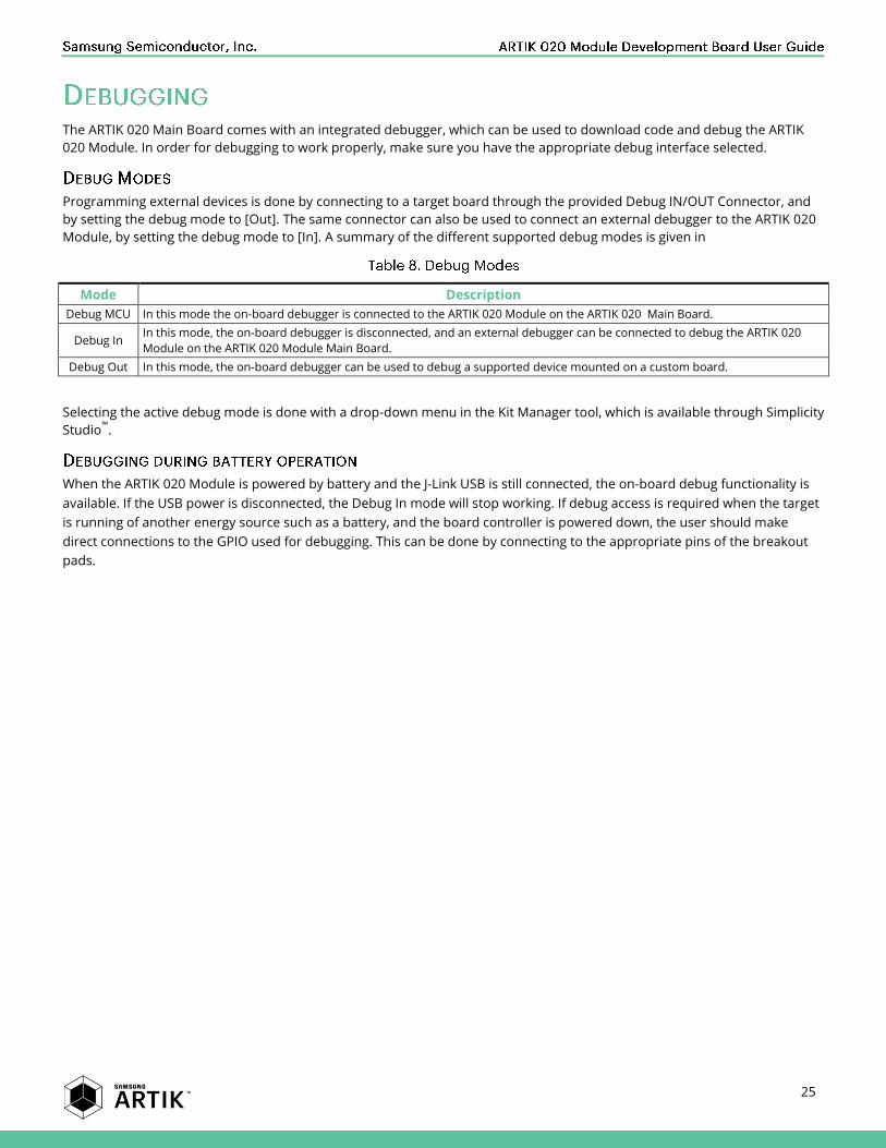
The ARTIK 020 Main Board comes with an integrated debugger, which can be used to download code and debug the ARTIK
020 Module. In order for debugging to work properly, make sure you have the appropriate debug interface selected.
Programming external devices is done by connecting to a target board through the provided Debug IN/OUT Connector, and
by setting the debug mode to [Out]. The same connector can also be used to connect an external debugger to the ARTIK 020
Module, by setting the debug mode to [In]. A summary of the different supported debug modes is given in
Mode Description
Debug MCU In this mode the on-board debugger is connected to the ARTIK 020 Module on the ARTIK 020 Main Board.
Debug In In this mode, the on-board debugger is disconnected, and an external debugger can be connected to debug the ARTIK 020
Module on the ARTIK 020 Module Main Board.
Debug Out In this mode, the on-board debugger can be used to debug a supported device mounted on a custom board.
Selecting the active debug mode is done with a drop-down menu in the Kit Manager tool, which is available through Simplicity
Studio™
.
When the ARTIK 020 Module is powered by battery and the J-Link USB is still connected, the on-board debug functionality is
available. If the USB power is disconnected, the Debug In mode will stop working. If debug access is required when the target
is running of another energy source such as a battery, and the board controller is powered down, the user should make
direct connections to the GPIO used for debugging. This can be done by connecting to the appropriate pins of the breakout
pads.

26
Please contact a sales representative in your area using the ARTIK official webpage – http://www.artik.io.

27
INFORMATION IN THIS DOCUMENT IS PROVIDED IN CONNECTION WITH THE SAMSUNG ARTIK™ DEVELOPMENT KIT AND ALL
RELATED PRODUCTS, UPDATES, AND DOCUMENTATION (HEREINAFTER “SAMSUNG PRODUCTS”). NO LICENSE, EXPRESS OR
IMPLIED, BY ESTOPPEL OR OTHERWISE, TO ANY INTELLECTUAL PROPERTY RIGHTS IS GRANTED BY THIS DOCUMENT. THE
LICENSE AND OTHER TERMS AND CONDITIONS RELATED TO YOUR USE OF THE SAMSUNG PRODUCTS ARE GOVERNED
EXCLUSIVELY BY THE SAMSUNG ARTIK™ DEVELOPER LICENSE AGREEMENT THAT YOU AGREED TO WHEN YOU REGISTERED AS
A DEVELOPER TO RECEIVE THE SAMSUNG PRODUCTS. EXCEPT AS PROVIDED IN THE SAMSUNG ARTIK™ DEVELOPER LICENSE
AGREEMENT, SAMSUNG ELECTRONICS CO., LTD. AND ITS AFFILIATES (COLLECTIVELY, “SAMSUNG”) AND ITS SUPPLIERS
ASSUME NO LIABILITY WHATSOEVER, INCLUDING WITHOUT LIMITATION CONSEQUENTIAL OR INCIDENTAL DAMAGES, AND
SAMSUNG DISCLAIMS ANY EXPRESS OR IMPLIED WARRANTY, ARISING OUT OF OR RELATED TO YOUR SALE, APPLICATION
AND/OR USE OF SAMSUNG PRODUCTS INCLUDING LIABILITY OR WARRANTIES RELATED TO FITNESS FOR A PARTICULAR
PURPOSE, MERCHANTABILITY, OR INFRINGEMENT OF ANY PATENT, COPYRIGHT, OR OTHER INTELLECTUAL PROPERTY RIGHT.
SAMSUNG RESERVES THE RIGHT TO CHANGE PRODUCTS, INFORMATION, DOCUMENTATION AND SPECIFICATIONS WITHOUT
NOTICE. THIS INCLUDES MAKING CHANGES TO THIS DOCUMENTATION AT ANY TIME WITHOUT PRIOR NOTICE.
CHARACTERIZATION DATA, AVAILABLE MODULES AND PERIPHERALS, MEMORY SIZES AND MEMORY ADDRESSES REFER TO
EACH SPECIFIC DEVICE, AND "TYPICAL" PARAMETERS PROVIDED CAN AND DO VARY IN DIFFERENT APPLICATIONS. THIS
DOCUMENTATION IS PROVIDED FOR REFERENCE PURPOSES ONLY, AND ALL INFORMATION DISCUSSED HEREIN IS PROVIDED
ON AN “AS IS” BASIS, WITHOUT WARRANTIES OF ANY KIND. SAMSUNG AND ITS SUPPLIERS ASSUME NO RESPONSIBILITY FOR
POSSIBLE ERRORS OR OMISSIONS, OR FOR ANY CONSEQUENCES FROM THE USE OF THE DOCUMENTATION CONTAINED
HEREIN.
Samsung Products are not intended for use in medical, life support, critical care, safety equipment, or similar applications
where product failure could result in loss of life or personal or physical harm, or any military or defense application, or any
governmental procurement to which special terms or provisions may apply. Samsung Products shall under no circumstances
be used in weapons of mass destruction including (but not limited to) nuclear, biological or chemical weapons, or missiles
capable of delivering such weapons.
This document and all information discussed herein remain the sole and exclusive property of Samsung. All brand names,
trademarks and registered trademarks belong to their respective owners. For updates or additional information about
Samsung ARTIK™, contact the Samsung ARTIK™ team via the Samsung ARTIK™ website at www.artik.io. Silicon Laboratories
Inc.®, Silicon Labs®, SiLabs®, Simplicity Studio™, EFR32™, LEUART™ and others are trademarks or registered trademarks of
Silicon Laboratories Inc. ARM and Cortex-M4 are trademarks or registered trademarks of ARM Holdings.
Copyright © 2016 Samsung Electronics Co., Ltd.
All rights reserved. No part of this publication may be reproduced, stored in a retrieval system, or transmitted in any form or
by any means, electric or mechanical, by photocopying, recording, or otherwise, without the prior written consent of
Samsung Electronics.