Embed Size (px)
Citation preview
Doc.No. Rev.No Page / 34LTN156AT22-001 104-A03-S-110406
Approval
Samsung Secret
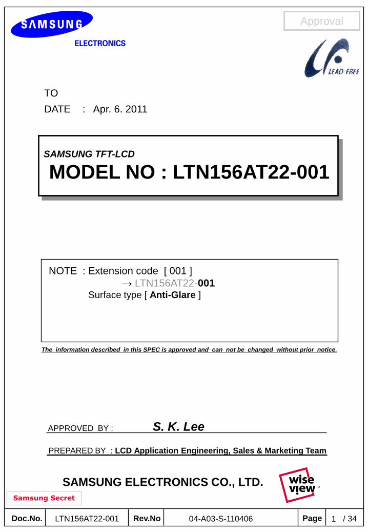
TO
DATE : Apr. 6. 2011
SAMSUNG TFT-LCD
MODEL NO : LTN156AT22-001
SAMSUNG ELECTRONICS CO., LTD.
APPROVED BY : S. K. Lee
PREPARED BY : LCD Application Engineering, Sales & Marketing Team
The information described in this SPEC is approved and can not be changed without prior notice.
NOTE : Extension code [ 001 ]
→ LTN156AT22-001Surface type [ Anti-Glare ]
Doc.No. Rev.No Page / 34LTN156AT22-001 204-A03-S-110406
Approval
Samsung Secret
CONTENTS
Revision History
General Description
1. Absolute Maximum Ratings
1.1 Absolute Ratings of environment
1.2 Electrical Absolute Ratings
2. Optical Characteristics
3. Electrical Characteristics
3.1 TFT LCD Module
3.2 Backlight Unit
3.3 LED Driver
4. Block Diagram
4.1 TFT LCD Module
5. Input Terminal Pin Assignment
5.1 Input Signal & Power
5.2 LVDS Interface
5.3 LVDS characteristics
5.4 Input Signals, Basic Display Colors and Gray Scale of Each Color.
5.5 Pixel format
6. Interface Timing
6.1 Timing Parameters
6.2 Timing Diagrams of interface Signal
6.3 Power ON/OFF Sequence
7. Outline Dimension
8. Packing
9. Markings & Others
10. General Precautions
11. EDID
- - - - - - - - - - - - - - - - - - - ( 3 )
- - - - - - - - - - - - - - - - - - - ( 5 )
- - - - - - - - - - - - - - - - - - - ( 6 )
- - - - - - - - - - - - - - - - - - - ( 8 )
- - - - - - - - - - - - - - - - - - - ( 11 )
- - - - - - - - - - - - - - - - - - - ( 14 )
- - - - - - - - - - - - - - - - - - - ( 15 )
- - - - - - - - - - - - - - - - - - - ( 21 )
- - - - - - - - - - - - - - - - - - - ( 23 )
-- - - - - - - - - - - - - - - - - - ( 26 )
-- - - - - - - - - - - - - - - - - - ( 28)
-- - - - - - - - - - - - - - - - - - ( 30 )
- - - - - - - - - - - - - - - - - - - ( 32 )
Doc.No. Rev.No Page / 34LTN156AT22-001 304-A03-S-110406
Approval
Samsung Secret
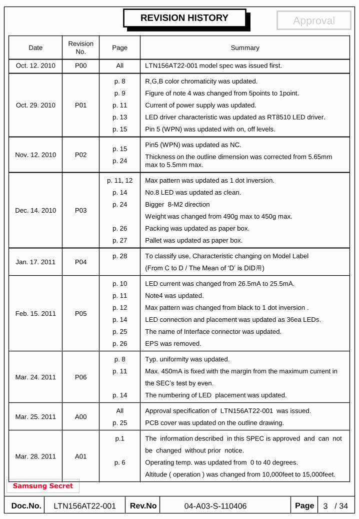
REVISION HISTORY
DateRevision
No.Page Summary
Oct. 12. 2010 P00 All LTN156AT22-001 model spec was issued first.
Oct. 29. 2010 P01
p. 8
p. 9
p. 11
p. 13
p. 15
R,G,B color chromaticity was updated.
Figure of note 4 was changed from 5points to 1point.
Current of power supply was updated.
LED driver characteristic was updated as RT8510 LED driver.
Pin 5 (WPN) was updated with on, off levels.
Nov. 12. 2010 P02p. 15
p. 24
Pin5 (WPN) was updated as NC.
Thickness on the outline dimension was corrected from 5.65mm
max to 5.5mm max.
Dec. 14. 2010 P03
p. 11, 12
p. 14
p. 24
p. 26
p. 27
Max pattern was updated as 1 dot inversion.
No.8 LED was updated as clean.
Bigger 8-M2 direction
Weight was changed from 490g max to 450g max.
Packing was updated as paper box.
Pallet was updated as paper box.
Jan. 17. 2011 P04p. 28 To classify use, Characteristic changing on Model Label
(From C to D / The Mean of „D‟ is DID用)
Feb. 15. 2011 P05
p. 10
p. 11
p. 12
p. 14
p. 25
p. 26
LED current was changed from 26.5mA to 25.5mA.
Note4 was updated.
Max pattern was changed from black to 1 dot inversion .
LED connection and placement was updated as 36ea LEDs.
The name of Interface connector was updated.
EPS was removed.
Mar. 24. 2011 P06
p. 8
p. 11
p. 14
Typ. uniformity was updated.
Max. 450mA is fixed with the margin from the maximum current in
the SEC‟s test by even.
The numbering of LED placement was updated.
Mar. 25. 2011 A00All
p. 25
Approval specification of LTN156AT22-001 was issued.
PCB cover was updated on the outline drawing.
Mar. 28. 2011 A01
p.1
p. 6
The information described in this SPEC is approved and can not
be changed without prior notice.
Operating temp. was updated from 0 to 40 degrees.
Altitude ( operation ) was changed from 10,000feet to 15,000feet.
Doc.No. Rev.No Page / 34LTN156AT22-001 404-A03-S-110406
Approval
Samsung Secret
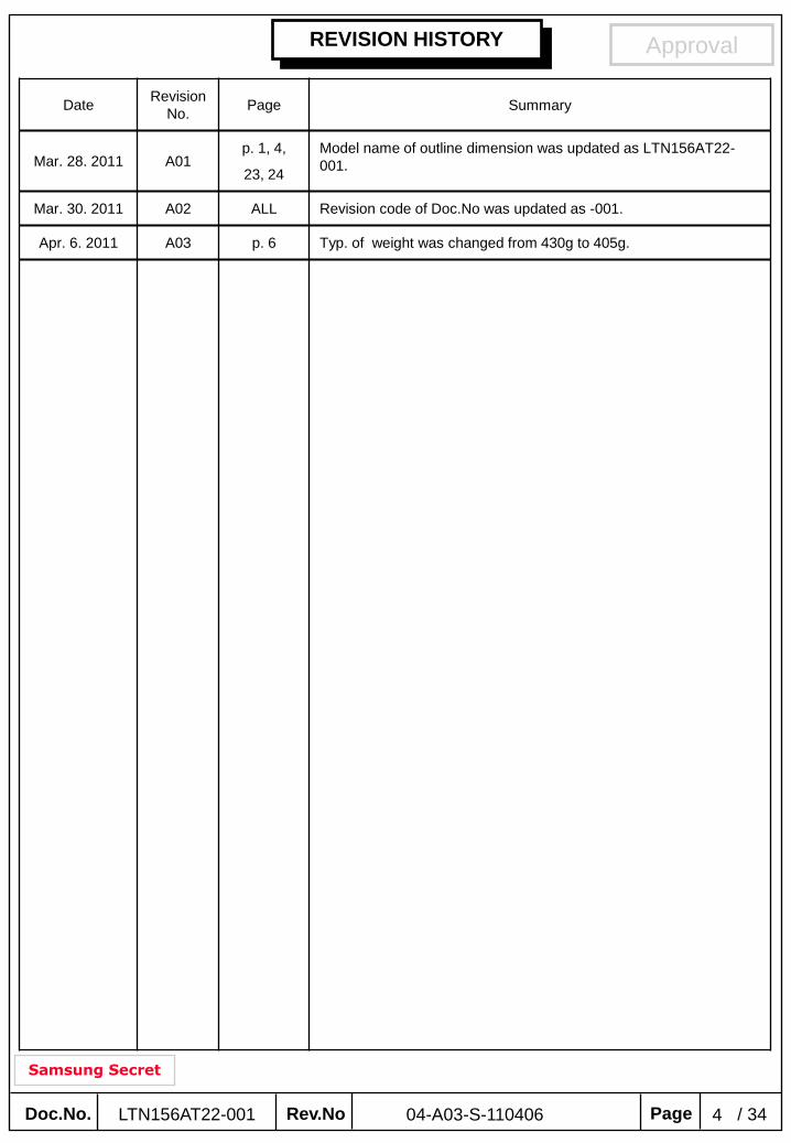
REVISION HISTORY
DateRevision
No.Page Summary
Mar. 28. 2011 A01p. 1, 4,
23, 24
Model name of outline dimension was updated as LTN156AT22-
001.
Mar. 30. 2011 A02 ALL Revision code of Doc.No was updated as -001.
Apr. 6. 2011 A03 p. 6 Typ. of weight was changed from 430g to 405g.
Doc.No. Rev.No Page / 34LTN156AT22-001 504-A03-S-110406
Approval
Samsung Secret
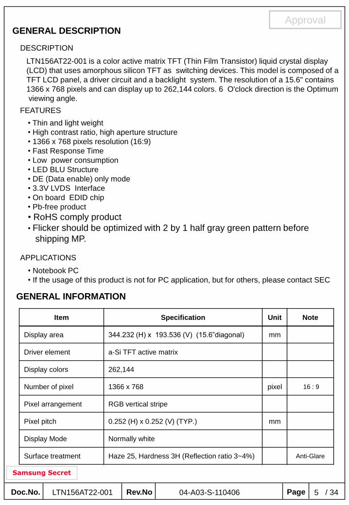
GENERAL DESCRIPTION
DESCRIPTION
LTN156AT22-001 is a color active matrix TFT (Thin Film Transistor) liquid crystal display
(LCD) that uses amorphous silicon TFT as switching devices. This model is composed of a
TFT LCD panel, a driver circuit and a backlight system. The resolution of a 15.6" contains
1366 x 768 pixels and can display up to 262,144 colors. 6 O'clock direction is the Optimum
viewing angle.
APPLICATIONS
• Notebook PC
• If the usage of this product is not for PC application, but for others, please contact SEC
GENERAL INFORMATION
FEATURES
• Thin and light weight
• High contrast ratio, high aperture structure
• 1366 x 768 pixels resolution (16:9)
• Fast Response Time
• Low power consumption
• LED BLU Structure
• DE (Data enable) only mode
• 3.3V LVDS Interface
• On board EDID chip
• Pb-free product
• RoHS comply product
• Flicker should be optimized with 2 by 1 half gray green pattern before
shipping MP.
Item Specification Unit Note
Display area 344.232 (H) x 193.536 (V) (15.6”diagonal) mm
Driver element a-Si TFT active matrix
Display colors 262,144
Number of pixel 1366 x 768 pixel 16 : 9
Pixel arrangement RGB vertical stripe
Pixel pitch 0.252 (H) x 0.252 (V) (TYP.) mm
Display Mode Normally white
Surface treatment Haze 25, Hardness 3H (Reflection ratio 3~4%) Anti-Glare
Doc.No. Rev.No Page / 34LTN156AT22-001 604-A03-S-110406
Approval
Samsung Secret
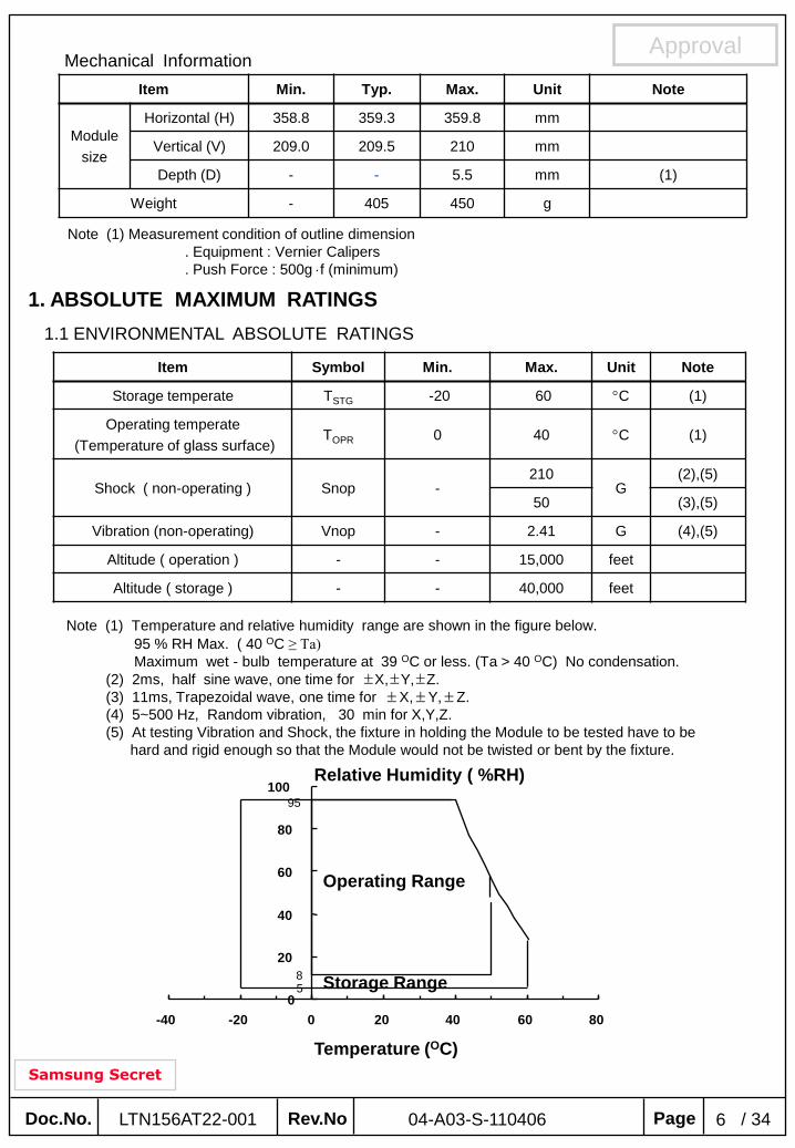
Mechanical Information
Item Min. Typ. Max. Unit Note
Module
size
Horizontal (H) 358.8 359.3 359.8 mm
Vertical (V) 209.0 209.5 210 mm
Depth (D) - - 5.5 mm (1)
Weight - 405 450 g
Note (1) Measurement condition of outline dimension
. Equipment : Vernier Calipers
. Push Force : 500g f (minimum)
1. ABSOLUTE MAXIMUM RATINGS
1.1 ENVIRONMENTAL ABSOLUTE RATINGS
0
20
40
60
80
100
-40 -20 0 20 40 60 80
5
95
Operating Range
Storage Range
Relative Humidity ( %RH)
Temperature (OC)
8
Item Symbol Min. Max. Unit Note
Storage temperate TSTG -20 60 C (1)
Operating temperate
(Temperature of glass surface)TOPR 0 40 C (1)
Shock ( non-operating ) Snop -210
G(2),(5)
50 (3),(5)
Vibration (non-operating) Vnop - 2.41 G (4),(5)
Altitude ( operation ) - - 15,000 feet
Altitude ( storage ) - - 40,000 feet
Note (1) Temperature and relative humidity range are shown in the figure below.
95 % RH Max. ( 40 OC ≥ Ta)
Maximum wet - bulb temperature at 39 OC or less. (Ta > 40 OC) No condensation.
(2) 2ms, half sine wave, one time for ±X,±Y,±Z.
(3) 11ms, Trapezoidal wave, one time for ±X,±Y,±Z.
(4) 5~500 Hz, Random vibration, 30 min for X,Y,Z.
(5) At testing Vibration and Shock, the fixture in holding the Module to be tested have to be
hard and rigid enough so that the Module would not be twisted or bent by the fixture.
Doc.No. Rev.No Page / 34LTN156AT22-001 704-A03-S-110406
Approval
Samsung Secret
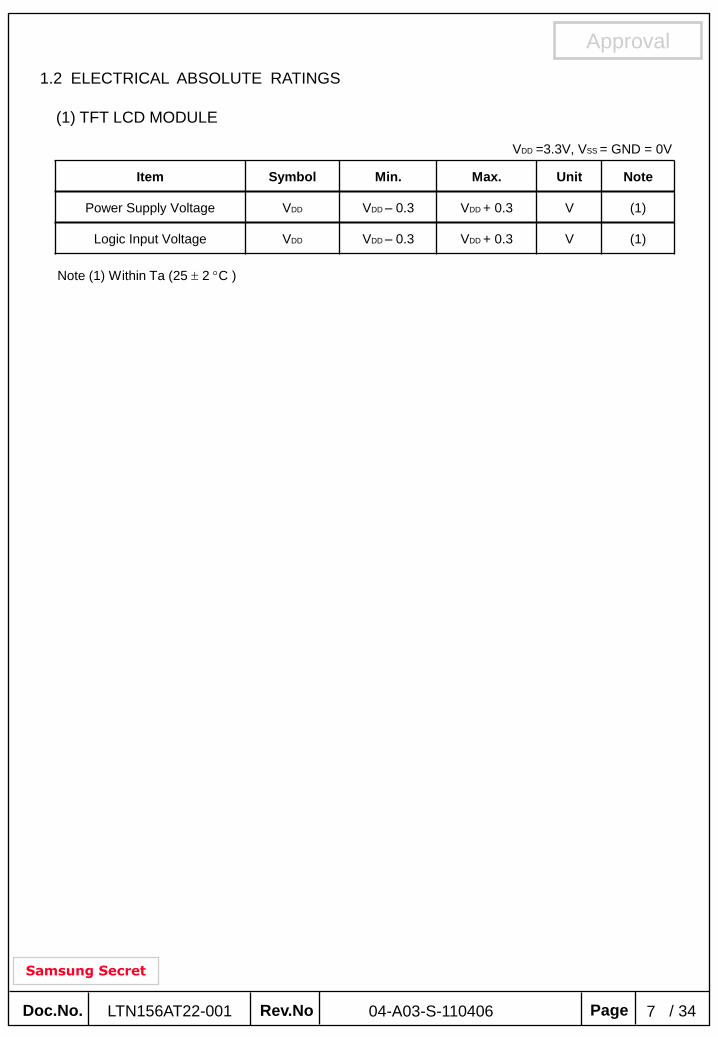
1.2 ELECTRICAL ABSOLUTE RATINGS
(1) TFT LCD MODULE
Note (1) Within Ta (25 2 C )
VDD =3.3V, VSS = GND = 0V
Item Symbol Min. Max. Unit Note
Power Supply Voltage VDD VDD – 0.3 VDD + 0.3 V (1)
Logic Input Voltage VDD VDD – 0.3 VDD + 0.3 V (1)
Doc.No. Rev.No Page / 34LTN156AT22-001 804-A03-S-110406
Approval
Samsung Secret
2. OPTICAL CHARACTERISTICS
The following items are measured under stable conditions. The optical characteristics
should be measured in a dark room or equivalent state with the methods shown in Note (5).
Measuring equipment : TOPCON SR-3
* Ta = 25 2 C, VDD=3.3V, fv= 60Hz, fDCLK = 72.33 MHz, PWM duty = 100%
Item SymbolConditio
nMin. Typ. Max Unit Note
Contrast Ratio CR1 center
point300 500 - -
(1), (2),
(5)
Response Time at Ta
( Rising + Falling )TRT -
16
( 6.75 +
9.25 )
25 msec (1), (3)
Average Luminance
of WhiteYL,AVE
1 center
point190 220 - cd/m2
PWM duty
= 100%
(1), (4)
Color
Chromaticity
( CIE )
RedRX
Normal
Viewing
Angle
= 0
= 0
0.585 0.615 0.645
-
RY 0.325 0.355 0.385
GreenGX 0.305 0.335 0.365
GY 0.580 0.610 0.640
BlueBX 0.120 0.150 0.180
BY 0.070 0.100 0.130
WhiteWX 0.283 0.313 0.343
WY 0.299 0.329 0.359
Viewing
Angle
Hor.L
CR 10
40 45 -
Degrees (1), (5)
SR-3
R 40 45 -
Ver. H 10 15 -
L 30 35 -
Color Gamut - 60 - %
13 Points
White VariationL - 1.6 1.7 - (6)
Doc.No. Rev.No Page / 34LTN156AT22-001 904-A03-S-110406
Approval
Samsung Secret
Note 3) Definition of Response time :
Note 1) Definition of Viewing Angle : Viewing angle range(10 C/R)
Note 4) Definition of Average Luminance of White : measure the luminance of white at 1 point.
6 O‟clock
direction
Normal Line
L
R
H L 12 O‟clock
direction
R =90o
L =90o
= 0o,
x
x'y'
y
= 0o
H = 90o
L= 90o
Display data Black(TFT ON)White(TFT OFF) White(TFT OFF)
Optical
Response
100%
90%
10%
0%
TR TF
Time
CR = CR(4) + CR(5) + CR(7) + CR(9) + CR(10)
Note 2) Definition of Contrast Ratio (CR) : Ratio of gray max (Gmax) ,gray min (Gmin)
at 5 points(4, 5, 7, 9, 10)
5
Points : , , , , at the figure of Note (6). 4 9 1075
: test point
VIEW AREA
(192)
(384)
(576)
(lines)
(342) ( 683) (1024)
7
. Center 1point of White ( YL,AVE )
Y,CENTER = YL7
Doc.No. Rev.No Page / 34LTN156AT22-001 1004-A03-S-110406
Approval
Samsung Secret
[ Optical characteristics measurement setup ]
Center of the screen
TFT-LCD module LCD panel
Photo-detector
( TOPCON SR-3 )
50 cmField = 2
Note 5) After stabilizing and leaVBLg the panel alone at a given temperature for 30 min , the measurement
should be executed. Measurement should be executed in a stable, windless,and dark room.
30 min after lighting the backlight. This should be measured in the center of screen.
LED current : 25.5 mA
Environment condition : Ta = 25 2 C
Maximum luminance of 13 points
Minimum luminance of 13 points
Note 6) Definition of 13 points white variation ( L ), [ ~ ]1 13
L =
: test point
342 683 1024
192
384
576
(lines)
10mm
10mm
10mm 10mm
4
2
5
3
68
10 9
13 12 11
1
7
Doc.No. Rev.No Page / 34LTN156AT22-001 1104-A03-S-110406
Approval
Samsung Secret
3. ELECTRICAL CHARACTERISTICS
3.1 TFT LCD MODULE
Note (1) Display data pins and timing signal pins should be connected.( GND = 0V )
(2) fV = 60Hz, fDCLK = 72.33 MHZ, VDD = 3.3V , DC Current.
(3) Power dissipation pattern
(4) Max. 450mA is fixed with the margin from the maximum current in the SEC‟s test by even.
*a) White Pattern *b) Mosaic Pattern
Display Brightest Gray Level
Display Darkest Gray Level
VIEW AREA
Ta= 25 2C
Item Symbol Min. Typ. Max. Unit Note
Voltage of Power Supply VDD 3.0 3.3 3.6 V
Differential Input
Voltage for LVDS
Receiver Threshold
High VIH - - +100 mVVCM = +1.2V
( +/- 10% )
Low VIL -100 - - mV
Vsync Frequency fv - 60 - Hz
Hsync Frequency fH - 47.4 - KHz
Main Frequency fDCLK 67.5 72.33 80 MHz
EDID Input Voltage VEDID 2.5 3.3 5.0 V
EDID Input Current IEDID - 0.8 1.0 mA
Skew PS -500 - +500 ps fDCLK =72.33Mhz
Rush Current IRUSH - - 1.5 A (4)
Current of Power
Supply
White
IDD
- 200 - mA (2),(3)*a
Mosaic - 220 - mA (2),(3)*b
V. Stripe - 350 - mA (2),(3)*c
Black - 200 - mA (2),(3)*d
1 dot - 400 450 mA (2),(3),(4)*e
Doc.No. Rev.No Page / 34LTN156AT22-001 1204-A03-S-110406
Approval
Samsung Secret
4) Rush current measurement condition
VDD rising time is 470us
3.3V
GND
0.9VDD
0.1VDD
470us
3.3V
12V
VDD ( LCD INPUT)
CONTROL SIGNAL
(HIGH to LOW)M2
2SK1399
M1
2SK1059
R2
1K
C2
10000pFC3
1uF
R3
47K
R1
47K
FUSEC1
1uF
*c) 1dot Vertical stripe pattern
R G B R G B R G B R G
G B R G B R G B R G
R G B R G B R G B R G
G B R G B R G B R GR
R
*e) Max pattern : 1dot inversion
*d) Black
+
-
+
-
+ +
+ +
- -
- -
- -
+ +
- -
+ +
+ +
- -
-
+
+
+ -+
+
+
-
-
- + + -+ -
+ -
- +
- - + -
Doc.No. Rev.No Page / 34LTN156AT22-001 1304-A03-S-110406
Approval
Samsung Secret
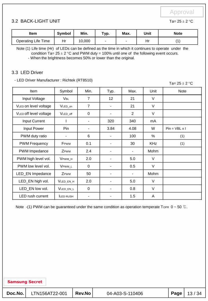
3.2 BACK-LIGHT UNIT
Item Symbol Min. Typ. Max. Unit Note
Operating Life Time Hr 10,000 - - Hr (1)
Ta= 25 2 C
3.3 LED Driver
- LED Driver Manufacturer : Richtek (RT8510)
Note (1) Life time (Hr) of LEDs can be defined as the time in which it continues to operate under the
condition Ta= 25 2 C and PWM duty = 100% until one of the following event occurs.
- When the brightness becomes 50% or lower than the original.
Ta= 25 2 C
Note -(1) PWM can be guaranteed under the same condition as operation temperate TOPR 0 ~ 50 ℃.
Item Symbol Min. Typ. Max. Unit Note
Input Voltage VBL 7 12 21 V
VLED on level voltage VLED_on 7 - 21 V
VLED off level voltage VLED_off 0 - 2 V
Input Current I - 320 340 mA
Input Power Pin - 3.84 4.08 W Pin = VBL x I
PWM duty ratio - 6 - 100 % (1)
PWM Frequency FPWM 0.1 - 30 KHz (1)
PWM Impedance ZPWM 2.4 - - Mohm
PWM high level vol. VPWM_H 2.0 - 5.0 V
PWM low level vol. VPWM_L 0 - 0.5 V
LED_EN Impedance ZPWM 50 - - Mohm
LED_EN high vol. VLED_EN_H 2.0 - 5.0 V
LED_EN low vol. VLED_EN_L 0 - 0.8 V
LED rush current ILED RUSH - - 1.5 A
Doc.No. Rev.No Page / 34LTN156AT22-001 1404-A03-S-110406
Approval
Samsung Secret
4. BLOCK DIAGRAM
4.1 TFT LCD Module
LVDS Input/LCDS Output
Timing Controller
15.6” HD
TFT-LCD Panel
Source
Driver
IC
TFT on Glass
DC-DCConverter
Control SignalVCOMGammaDVDDAVDDVon/Voff
Video Signal
Gamma
Generator
Input Connector
LVDS
VCOM
Generator
SOURCE PCB
mLVDS
EDID
EEPROM
I2 C bus
4.2 LED connection and placement
I-PEX 20455-040E-12
9
9 LEDs x 4 channels = Total 36 LEDs
9
……
..
LED 1, Channel 1-1
LED 2, Channel 2-1
LED 3, Channel 3-1
LED 4, Channel 4-1
LED 5, Channel 1-2
LED 36, Channel 4-9
LED Placement
Doc.No. Rev.No Page / 34LTN156AT22-001 1504-A03-S-110406
Approval
Samsung Secret
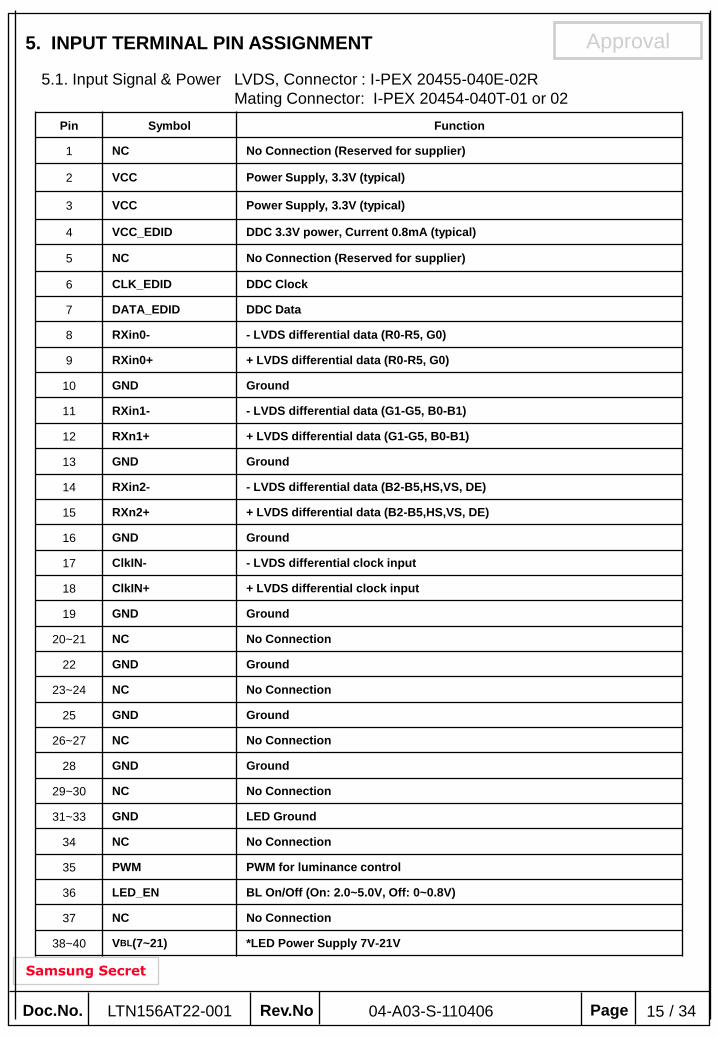
5. INPUT TERMINAL PIN ASSIGNMENT
Pin Symbol Function
1 NC No Connection (Reserved for supplier)
2 VCC Power Supply, 3.3V (typical)
3 VCC Power Supply, 3.3V (typical)
4 VCC_EDID DDC 3.3V power, Current 0.8mA (typical)
5 NC No Connection (Reserved for supplier)
6 CLK_EDID DDC Clock
7 DATA_EDID DDC Data
8 RXin0- - LVDS differential data (R0-R5, G0)
9 RXin0+ + LVDS differential data (R0-R5, G0)
10 GND Ground
11 RXin1- - LVDS differential data (G1-G5, B0-B1)
12 RXn1+ + LVDS differential data (G1-G5, B0-B1)
13 GND Ground
14 RXin2- - LVDS differential data (B2-B5,HS,VS, DE)
15 RXn2+ + LVDS differential data (B2-B5,HS,VS, DE)
16 GND Ground
17 ClkIN- - LVDS differential clock input
18 ClkIN+ + LVDS differential clock input
19 GND Ground
20~21 NC No Connection
22 GND Ground
23~24 NC No Connection
25 GND Ground
26~27 NC No Connection
28 GND Ground
29~30 NC No Connection
31~33 GND LED Ground
34 NC No Connection
35 PWM PWM for luminance control
36 LED_EN BL On/Off (On: 2.0~5.0V, Off: 0~0.8V)
37 NC No Connection
38~40 VBL(7~21) *LED Power Supply 7V-21V
5.1. Input Signal & Power LVDS, Connector : I-PEX 20455-040E-02R
Mating Connector: I-PEX 20454-040T-01 or 02
Doc.No. Rev.No Page / 34LTN156AT22-001 1604-A03-S-110406
Approval
Samsung Secret
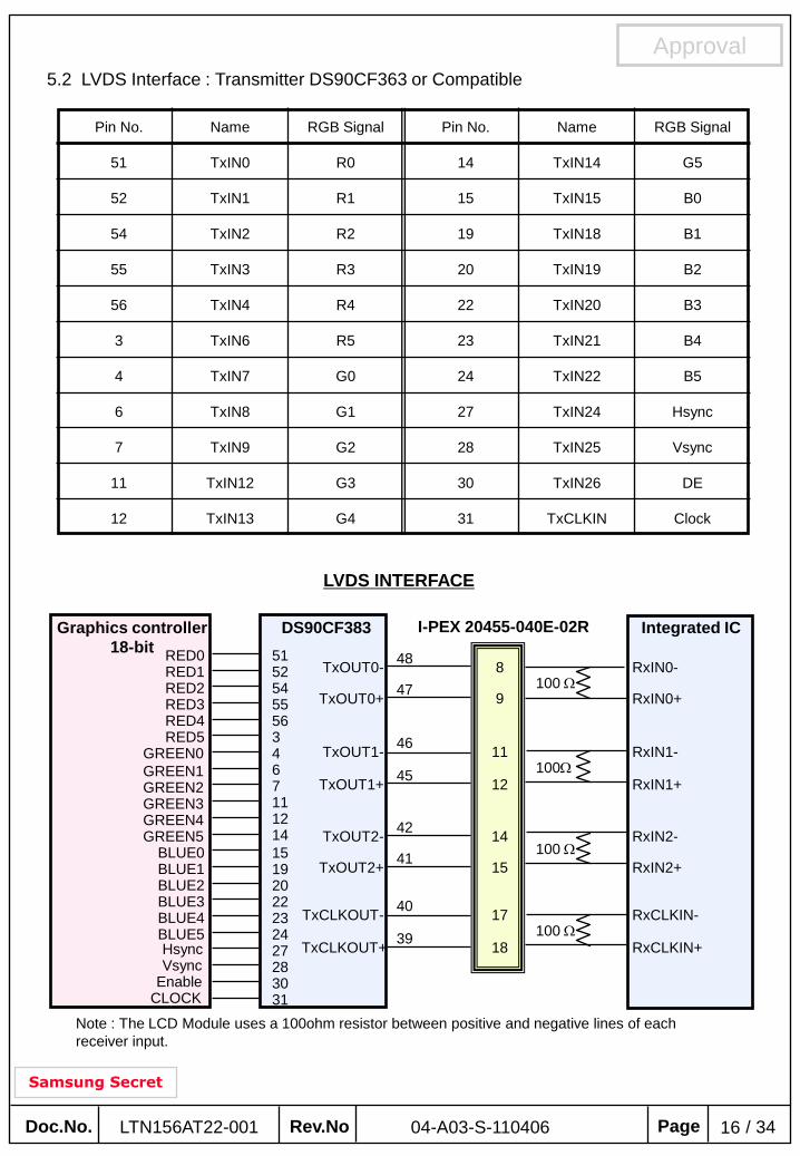
5.2 LVDS Interface : Transmitter DS90CF363 or Compatible
Note : The LCD Module uses a 100ohm resistor between positive and negative lines of each
receiver input.
Pin No. Name RGB Signal Pin No. Name RGB Signal
51 TxIN0 R0 14 TxIN14 G5
52 TxIN1 R1 15 TxIN15 B0
54 TxIN2 R2 19 TxIN18 B1
55 TxIN3 R3 20 TxIN19 B2
56 TxIN4 R4 22 TxIN20 B3
3 TxIN6 R5 23 TxIN21 B4
4 TxIN7 G0 24 TxIN22 B5
6 TxIN8 G1 27 TxIN24 Hsync
7 TxIN9 G2 28 TxIN25 Vsync
11 TxIN12 G3 30 TxIN26 DE
12 TxIN13 G4 31 TxCLKIN Clock
Graphics controller
18-bit
DS90CF383 Integrated IC
RED0RED1RED2RED3RED4RED5
GREEN0
Hsync
Enable
GREEN1GREEN2GREEN3GREEN4GREEN5
BLUE0BLUE1BLUE2BLUE3BLUE4BLUE5
Vsync
CLOCK
51525455563467111214
15192022232427283031
48
47
46
45
42
41
40
39
8
9
11
12
14
15
17
18
RxIN0-
RxIN0+
RxIN1-
RxIN1+
RxIN2-
RxIN2+
RxCLKIN-
RxCLKIN+
TxOUT0-
TxOUT0+
TxOUT1-
TxOUT1+
TxOUT2-
TxOUT2+
TxCLKOUT-
TxCLKOUT+
100
100
100
100
LVDS INTERFACE
I-PEX 20455-040E-02R
Doc.No. Rev.No Page / 34LTN156AT22-001 1704-A03-S-110406
Approval
Samsung Secret
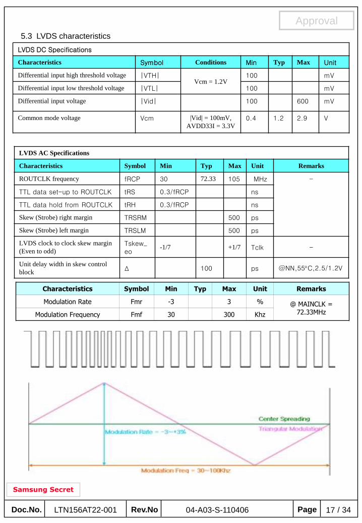
5.3 LVDS characteristics
LVDS DC Specifications
Characteristics Symbol Conditions Min Typ Max Unit
Differential input high threshold voltage |VTH|Vcm = 1.2V
100 mV
Differential input low threshold voltage |VTL| 100 mV
Differential input voltage |Vid| 100 600 mV
Common mode voltage Vcm |Vid| = 100mV,
AVDD33I = 3.3V0.4 1.2 2.9 V
LVDS AC Specifications
Characteristics Symbol Min Typ Max Unit Remarks
ROUTCLK frequency fRCP 30 72.33 105 MHz -
TTL data set-up to ROUTCLK tRS 0.3/fRCP ns
TTL data hold from ROUTCLK tRH 0.3/fRCP ns
Skew (Strobe) right margin TRSRM 500 ps
Skew (Strobe) left margin TRSLM 500 ps
LVDS clock to clock skew margin
(Even to odd)Tskew_eo
-1/7 +1/7 Tclk -
Unit delay width in skew control
blockΔ 100 ps @NN,55C,2.5/1.2V
Characteristics Symbol Min Typ Max Unit Remarks
Modulation Rate Fmr -3 3 % @ MAINCLK =72.33MHzModulation Frequency Fmf 30 300 Khz
Doc.No. Rev.No Page / 34LTN156AT22-001 1804-A03-S-110406
Approval
Samsung Secret
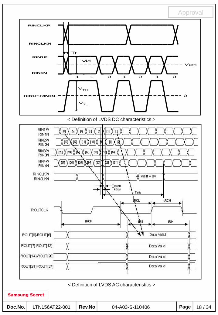
< Definition of LVDS AC characteristics >
VTL
RIN1P
RIN1P-RIN1N
Tr
Vcm
VTH
1 1 0 1 0 1 0
RINCLKP
Vid
RINCLKN
RIN1N
0
< Definition of LVDS DC characteristics >
Tclk
Doc.No. Rev.No Page / 34LTN156AT22-001 1904-A03-S-110406
Approval
Samsung Secret
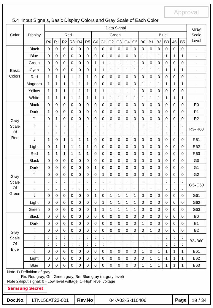
5.4 Input Signals, Basic Display Colors and Gray Scale of Each Color
Note 1) Definition of gray :
Rn: Red gray, Gn: Green gray, Bn: Blue gray (n=gray level)
Note 2)Input signal: 0 =Low level voltage, 1=High level voltage
Color Display
Data Signal Gray
Scale
Level
Red Green Blue
R0 R1 R2 R3 R4 R5 G0 G1 G2 G3 G4 G5 B0 B1 B2 B3 45 B5
Basic
Colors
Black 0 0 0 0 0 0 0 0 0 0 0 0 0 0 0 0 0 0 -
Blue 0 0 0 0 0 0 0 0 0 0 0 0 1 1 1 1 1 1 -
Green 0 0 0 0 0 0 1 1 1 1 1 1 0 0 0 0 0 0 -
Cyan 0 0 0 0 0 0 1 1 1 1 1 1 1 1 1 1 1 1 -
Red 1 1 1 1 1 1 0 0 0 0 0 0 0 0 0 0 0 0 -
Magenta 1 1 1 1 1 1 0 0 0 0 0 0 1 1 1 1 1 1 -
Yellow 1 1 1 1 1 1 1 1 1 1 1 1 0 0 0 0 0 0 -
White 1 1 1 1 1 1 1 1 1 1 1 1 1 1 1 1 1 1 -
Gray
Scale
Of
Red
Black 0 0 0 0 0 0 0 0 0 0 0 0 0 0 0 0 0 0 R0
Dark 1 0 0 0 0 0 0 0 0 0 0 0 0 0 0 0 0 0 R1
0 1 0 0 0 0 0 0 0 0 0 0 0 0 0 0 0 0 R2
: : : : : : : : : : : : : : : : : : :R3R60
: : : : : : : : : : : : : : : : : : :
1 0 1 1 1 1 0 0 0 0 0 0 0 0 0 0 0 0 R61
Light 0 1 1 1 1 1 0 0 0 0 0 0 0 0 0 0 0 0 R62
Red 1 1 1 1 1 1 0 0 0 0 0 0 0 0 0 0 0 0 R63
Gray
Scale
Of
Green
Black 0 0 0 0 0 0 0 0 0 0 0 0 0 0 0 0 0 0 G0
Dark 0 0 0 0 0 0 1 0 0 0 0 0 0 0 0 0 0 0 G1
0 0 0 0 0 0 0 1 0 0 0 0 0 0 0 0 0 0 G2
: : : : : : : : : : : : : : : : : : :G3G60
: : : : : : : : : : : : : : : : : : :
0 0 0 0 0 0 1 0 1 1 1 1 0 0 0 0 0 0 G61
Light 0 0 0 0 0 0 0 1 1 1 1 1 0 0 0 0 0 0 G62
Green 0 0 0 0 0 0 1 1 1 1 1 1 0 0 0 0 0 0 G63
Gray
Scale
Of
Blue
Black 0 0 0 0 0 0 0 0 0 0 0 0 0 0 0 0 0 0 B0
Dark 0 0 0 0 0 0 0 0 0 0 0 0 1 0 0 0 0 0 B1
0 0 0 0 0 0 0 0 0 0 0 0 0 1 0 0 0 0 B2
: : : : : : : : : : : : : : : : : : :B3B60
: : : : : : : : : : : : : : : : : : :
0 0 0 0 0 0 0 0 0 0 0 0 1 0 1 1 1 1 B61
Light 0 0 0 0 0 0 0 0 0 0 0 0 0 1 1 1 1 1 B62
Blue 0 0 0 0 0 0 0 0 0 0 0 0 1 1 1 1 1 1 B63
Doc.No. Rev.No Page / 34LTN156AT22-001 2004-A03-S-110406
Approval
Samsung Secret
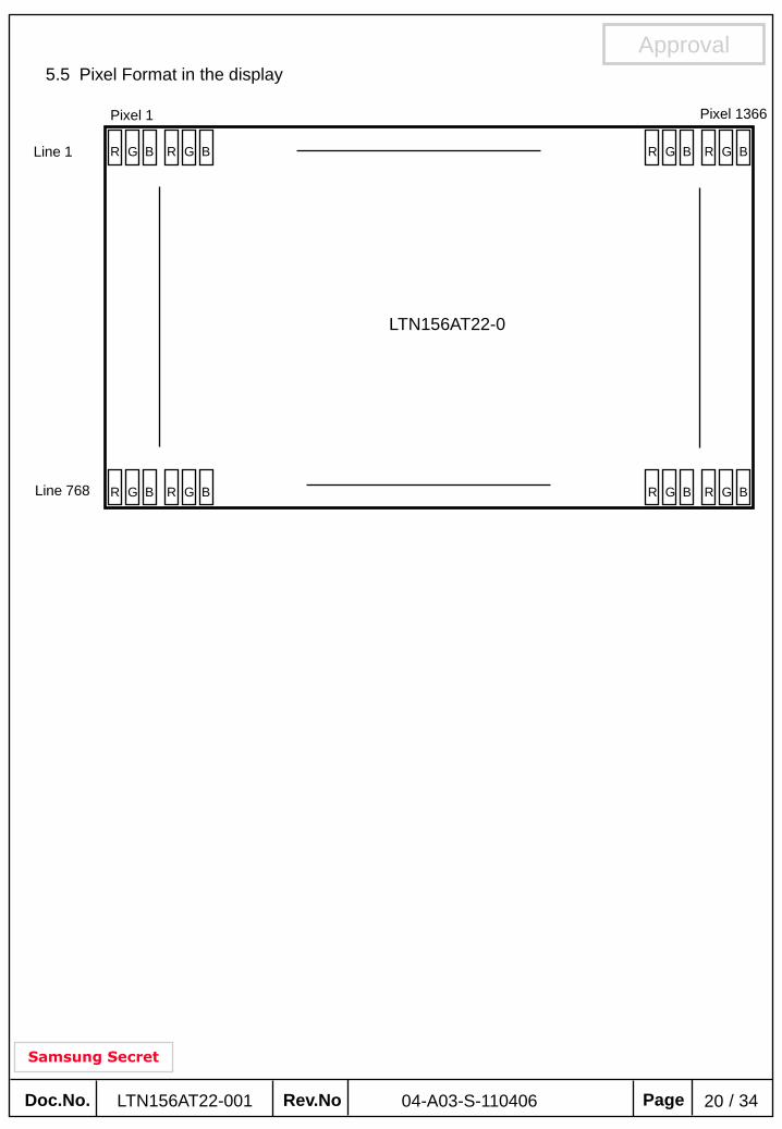
5.5 Pixel Format in the display
R G B R G B
Pixel 1
R G B R G B R G B R G B
R G B R G B
LTN156AT22-0
Line 1
Line 768
Pixel 1366
Doc.No. Rev.No Page / 34LTN156AT22-001 2104-A03-S-110406
Approval
Samsung Secret
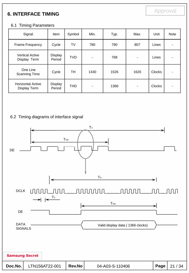
6. INTERFACE TIMING
6.1 Timing Parameters
6.2 Timing diagrams of interface signal
Signal Item Symbol Min. Typ. Max. Unit Note
Frame Frequency Cycle TV 780 790 807 Lines -
Vertical Active
Display Term
Display
PeriodTVD - 768 - Lines -
One Line
Scanning Time Cycle TH 1430 1526 1620 Clocks -
Horizontal Active
Display Term
Display
PeriodTHD - 1366 - Clocks -
TVD
TV
DE
TH
TC
THD
Valid display data ( 1366 clocks)
DCLK
DE
DATA
SIGNALS
Doc.No. Rev.No Page / 34LTN156AT22-001 2204-A03-S-110406
Approval
Samsung Secret
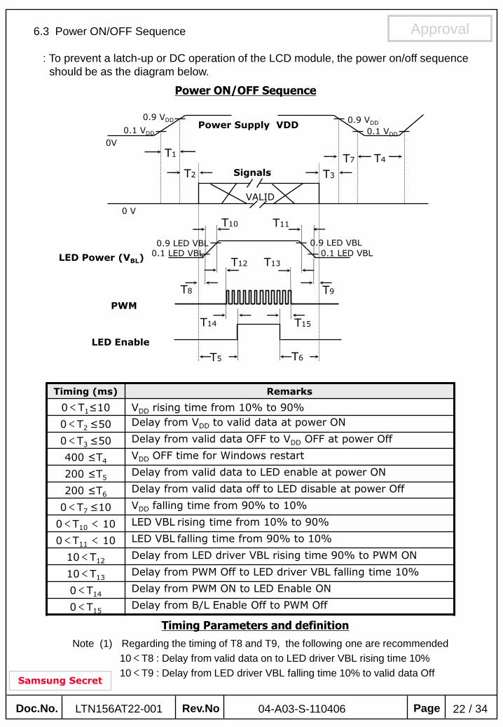
6.3 Power ON/OFF Sequence
: To prevent a latch-up or DC operation of the LCD module, the power on/off sequence
should be as the diagram below.
Power ON/OFF Sequence
0 V
0.9 VDD 0.9 VDD
0V
VALID
T3
T1
T2
T4
0.1 VDD 0.1 VDD
T6
LED Enable
T5
PWM
0.1 LED VBL
T8 T9
T14 T15
T11
Power Supply VDD
Signals
LED Power (VBL)
T7
T12
T10
T13
0.9 LED VBL 0.9 LED VBL
0.1 LED VBL
Timing (ms) Remarks
0<T1≤10 VDD rising time from 10% to 90%
0<T2 ≤50 Delay from VDD to valid data at power ON
0<T3 ≤50 Delay from valid data OFF to VDD OFF at power Off
400 ≤T4VDD OFF time for Windows restart
200 ≤T5Delay from valid data to LED enable at power ON
200 ≤T6Delay from valid data off to LED disable at power Off
0<T7 ≤10 VDD falling time from 90% to 10%
0<T10 < 10 LED VBL rising time from 10% to 90%
0<T11 < 10 LED VBL falling time from 90% to 10%
10<T12Delay from LED driver VBL rising time 90% to PWM ON
10<T13Delay from PWM Off to LED driver VBL falling time 10%
0<T14Delay from PWM ON to LED Enable ON
0<T15Delay from B/L Enable Off to PWM Off
Timing Parameters and definition
Note (1) Regarding the timing of T8 and T9, the following one are recommended
10<T8 : Delay from valid data on to LED driver VBL rising time 10%
10<T9 : Delay from LED driver VBL falling time 10% to valid data Off
Doc.No. Rev.No Page / 34LTN156AT22-001 2304-A03-S-110406
Approval
Samsung Secret
7. MECHANICAL OUTLINE DIMENSION
[ Refer to the next page ]
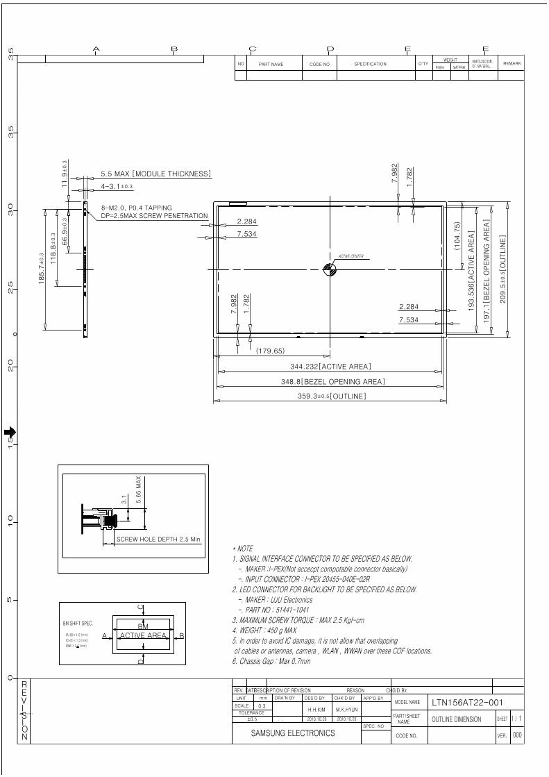
REVISION
LTN156AT22-001DES'D BYDRA'N BY CHK'D BY APP'D BYUNIT
SCALE
TOLERANCE
mm
. . . .
SPEC. NO
BMACTIVE AREAA B
CD
CODE NONO PART NAME SPECIFICATION Q'TY REMARK
3.1
SCREW HOLE DEPTH 2.5 Min
5.6
5 M
AX
(104.7
5)
359.3±0.5[OUTLINE]
344.232[ACTIVE AREA]
348.8[BEZEL OPENING AREA]
197.1
[BEZEL O
PEN
ING
AR
EA]
209.5±0.5
[OU
TLIN
E]
193.5
36[A
CTIV
E A
REA]
2.284
7.534
(179.65)
1.7
82
7.9
82
7.9
82
1.7
82
2.284
7.534
185.7±0.3
118.8±0.3
66.9±0.3
11.9±0.3
4-3.1±0.3
8-M2.0, P0.4 TAPPINGDP=2.5MAX SCREW PENETRATION
5.5 MAX [MODULE THICKNESS]

REVISION
DES'D BYDRA'N BY CHK'D BY APP'D BYUNIT
SCALE
TOLERANCE
mm
. .
SPEC. NO
CODE NONO PART NAME SPECIFICATION Q'TY REMARK
LTN156AT22-001
US C
CHR
Doc.No. Rev.No Page / 34LTN156AT22-001 2604-A03-S-110406
Approval
Samsung Secret
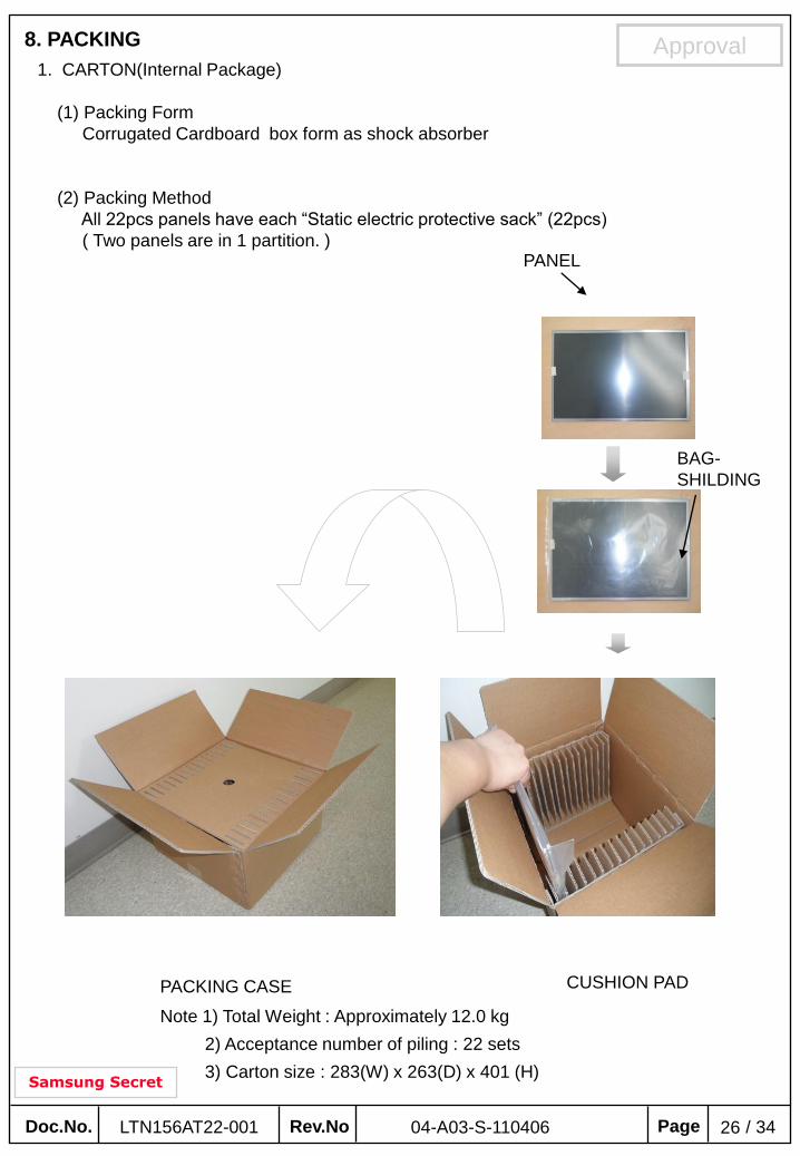
8. PACKING
1. CARTON(Internal Package)
(1) Packing Form
Corrugated Cardboard box form as shock absorber
(2) Packing Method
All 22pcs panels have each “Static electric protective sack” (22pcs)
( Two panels are in 1 partition. )
Note 1) Total Weight : Approximately 12.0 kg
2) Acceptance number of piling : 22 sets
3) Carton size : 283(W) x 263(D) x 401 (H)
PACKING CASE CUSHION PAD
PANEL
BAG-
SHILDING
Doc.No. Rev.No Page / 34LTN156AT22-001 2704-A03-S-110406
Approval
Samsung Secret
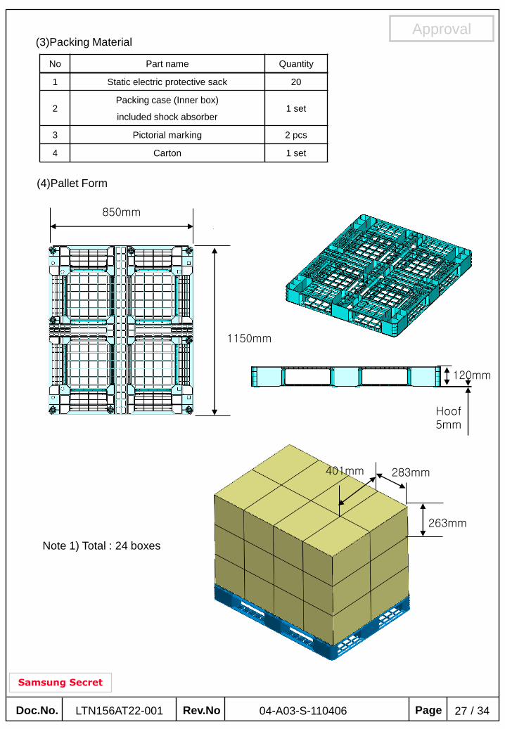
(3)Packing Material
No Part name Quantity
1 Static electric protective sack 20
2Packing case (Inner box)
included shock absorber1 set
3 Pictorial marking 2 pcs
4 Carton 1 set
(4)Pallet Form
1150mm
850mm
120mm
Hoof5mm
Note 1) Total : 24 boxes
283mm401mm
263mm
Doc.No. Rev.No Page / 34LTN156AT22-001 2804-A03-S-110406
Approval
Samsung Secret
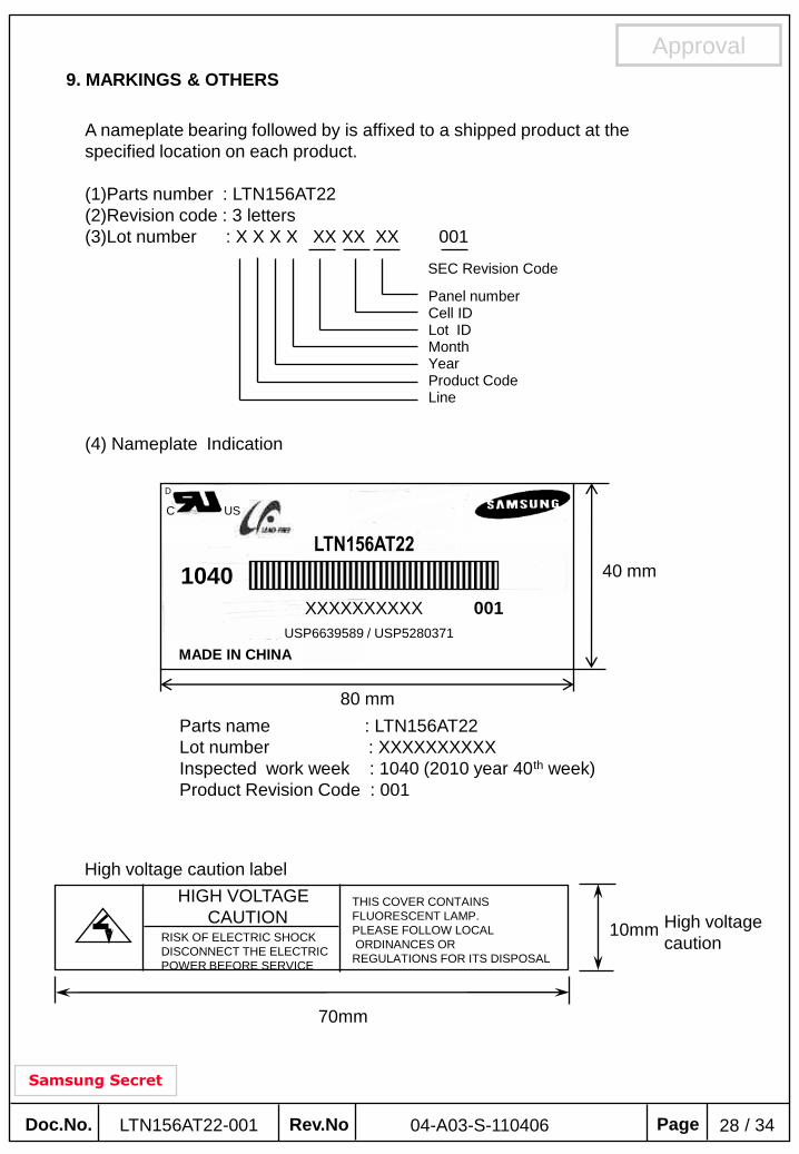
9. MARKINGS & OTHERS
A nameplate bearing followed by is affixed to a shipped product at the
specified location on each product.
(1)Parts number : LTN156AT22
(2)Revision code : 3 letters
(3)Lot number : X X X X XX XX XX 001
Panel numberCell IDLot IDMonthYearProduct CodeLine
SEC Revision Code
(4) Nameplate Indication
High voltage
caution
High voltage caution label
HIGH VOLTAGE
CAUTIONRISK OF ELECTRIC SHOCK
DISCONNECT THE ELECTRIC
POWER BEFORE SERVICE
10mm
70mm
THIS COVER CONTAINS
FLUORESCENT LAMP.
PLEASE FOLLOW LOCAL
ORDINANCES OR
REGULATIONS FOR ITS DISPOSAL
Parts name : LTN156AT22
Lot number : XXXXXXXXXX
Inspected work week : 1040 (2010 year 40th week)
Product Revision Code : 001
40 mm
80 mm
LTN156AT22
1040
XXXXXXXXXX 001
MADE IN CHINA
C US
D
USP6639589 / USP5280371
Doc.No. Rev.No Page / 34LTN156AT22-001 2904-A03-S-110406
Approval
Samsung Secret
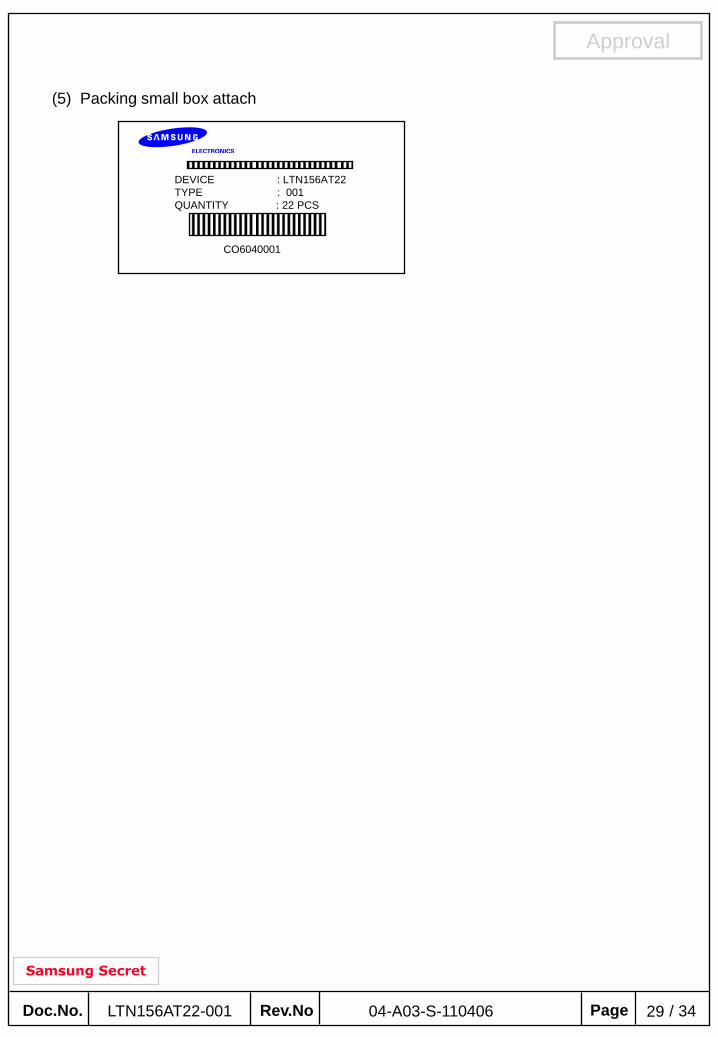
(5) Packing small box attach
DEVICE : LTN156AT22
TYPE : 001
QUANTITY : 22 PCS
CO6040001
Doc.No. Rev.No Page / 34LTN156AT22-001 3004-A03-S-110406
Approval
Samsung Secret
10. GENERAL PRECAUTIONS
1. Handling
(a) When the module is assembled, It should be attached to the system firmly
using every mounting holes. Be careful not to twist and bend the modules.
(b) Refrain from strong mechanical shock and / or any force to the module. In addition to
damage, this may cause improper operation or damage to the module and CCFT back-light.
(c) Note that polarizers are very fragile and could be easily damaged. Do not press or scratch
the surface harder than a HB pencil lead.
(d) Wipe off water droplets or oil immediately. If you leave the droplets for a long time,
Staining and discoloration may occur.
(e) If the surface of the polarizer is dirty, clean it using some absorbent cotton or soft cloth.
(f) The desirable cleaners are water, IPA (Isoprophyl Alcohol) or Hexane.
Do not use Ketone type materials(ex. Acetone), Ethyl alcohol, Toluene, Ethyl acid or Methyl
chloride. It might permanent damage to the polarizer due to chemical reaction.
(g) If the liquid crystal material leaks from the panel, it should be kept away from the eyes or
mouth . In case of contact with hands, legs or clothes, it must be washed away thoroughly
with soap.
(h) Protect the module from static , it may cause damage to the C-MOS Gate Array IC.
(i) Use fingerstalls with soft gloves in order to keep display clean during the incoming
inspection and assembly process.
(j) Do not disassemble the module.
(k) Do not pull or fold the lamp wire.
(l) Do not adjust the variable resistor which is located on the back side.
(m) Protection film for polarizer on the module shall be slowly peeled off just before use so
that the electrostatic charge can be minimized.
(n) Pins of I/F connector shall not be touched directly with bare hands.
Doc.No. Rev.No Page / 34LTN156AT22-001 3104-A03-S-110406
Approval
Samsung Secret
2. STORAGE
(a) Do not leave the module in high temperature, and high humidity for a long time.It is highly recommended to store the module with temperature from 0 to 35 C and relative humidity of less than 70%.
(b) Do not store the TFT-LCD module in direct sunlight.
(c) The module shall be stored in a dark place. It is prohibited to apply sunlight or fluorescentlight during the store.
3. OPERATION
(a) Do not connect,disconnect the module in the “ Power On” condition.
(b) Power supply should always be turned on/off by following item 6.3 “ Power on/off sequence “.
(c) Module has high frequency circuits. Sufficient suppression to the electromagnetic interference shall be done by system manufacturers. Grounding and shielding methodsmay be important to minimize the interference.
(d) The cable between the back-light connector and its inverter power supply shall be aminimized length and be connected directly . The longer cable between the back-lightand the inverter may cause lower luminance of lamp(CCFT) and may require higherstartup voltage (Vs).
(e) The standard limited warranty is only applicable when the module is used for general notebook applications. If used for purposes other than as specified, SEC is not to be held reliable for the defective operations. It is strongly recommended to contact SEC to find out fitness for a particular purpose.
( f ) When you connect a signal cable to LCD, remove an AC adapter by all means.In addition, to connect with keep the correct sequence, not to occur the short by left voltage.
4. OTHERS
(a) Ultra-violet ray filter is necessary for outdoor operation.
(b) Avoid condensation of water. It may result in improper operation or disconnection of electrode.
(c) Do not exceed the absolute maximum rating value. ( the supply voltage variation, input voltage variation, variation in part contents and environmental temperature, so on) Otherwise the module may be damaged.
(d) If the module displays the same pattern continuously for a long period of time,it can bethe situation when the image “sticks” to the screen.
(e) This module has its circuitry PCB‟s on the rear side and should be handled carefully in order not to be stressed.
Doc.No. Rev.No Page / 34LTN156AT22-001 3204-A03-S-110406
Approval
Samsung Secret
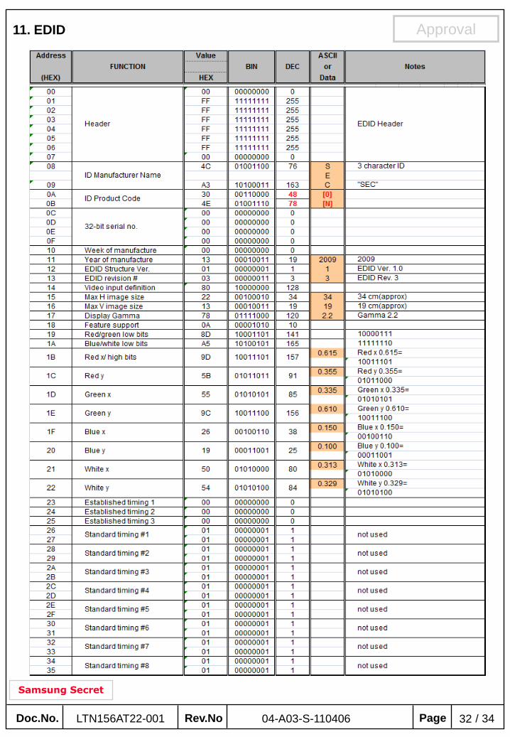
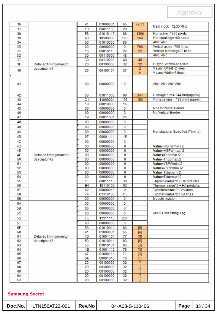
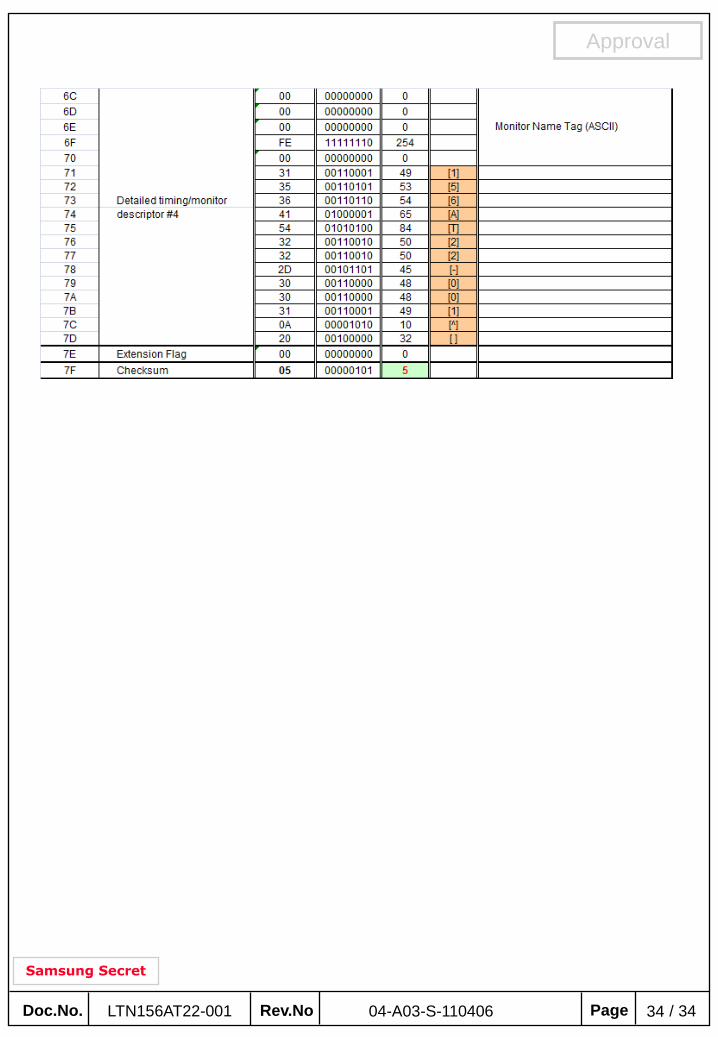
11. EDID
Doc.No. Rev.No Page / 34LTN156AT22-001 3304-A03-S-110406
Approval
Samsung Secret
Doc.No. Rev.No Page / 34LTN156AT22-001 3404-A03-S-110406
Approval
Samsung Secret


![SAMSUNG TFT-LCD MODEL A460HN08W(HD,60HZ) · LTY[Z]460HN05 is a color active matrix liquid crystal display (LCD) that uses amorphous silicon TFT(Thin Film Transistor) as switching](https://img.pdfslide.net/doc/110x75/5e813674375a7e757f1cdfd4/samsung-tft-lcd-model-a460hn08whd60hz-ltyz460hn05-is-a-color-active-matrix.jpg)