Embed Size (px)
Citation preview
www.semtech.com1
POWER MANAGEMENT
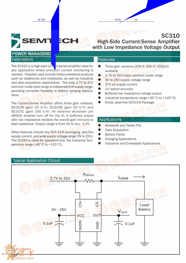
SC310High-Side Current-Sense Amplifier
with Low Impedance Voltage Output
Typical Application Circuit
Applications
Description FeaturesThe SC310 is a high-side current sense amplifier ideal forany application where precision current monitoring isneeded. Possible uses include battery-powered productssuch as cellphones and notebooks, as well as industrialand data acquisition applications. The wide 2.7V to 25Vcommon mode input range is independent of supply range,providing complete flexibility in battery sensing applica-tions.
The Current-Sense Amplifier offers three gain versions,SC310A (gain 20 V/V), SC310B (gain 50 V/V) andSC310C (gain 100 V/V). An external shutdown pin(SHDN) enables turn off for the IC. A buffered outputwith low impedance renders the overall gain immune toload resistance. Output range is from 0V to Vcc - 1.7V.
Other features include tiny SOT-23-6 packaging, very lowsupply current, and wide supply voltage range (3V to 25V).The SC310 is rated for operation over the Industrial Tem-perature range (-40°C to +125°C).
Three gain versions (20V/V, 50V/V, 100V/V) available 2.7V to 25V input common mode range 3V to 25V supply voltage range 270 μA supply current 1% typical accuracy Buffered low impedance voltage output Industrial temperature range (-40°C to +125°C) Small, lead-free SOT23-6 Package
Notebook and Tablet PCs Data Acquisition Battery Packs Charging Applications Industrial and Embedded Applications
June 4, 2007
0.1uF
2.7V to 25V
Load/Battery
CS
+
CS
-
SH
DN
OUT
GN
D
VCC
RSENSE ILOAD
VOUT3V - 25V
0.1uF
查询SC310供应商 捷多邦,专业PCB打样工厂,24小时加急出货
2© 2005 Semtech Corp. www.semtech.com
POWER MANAGEMENT
SC310
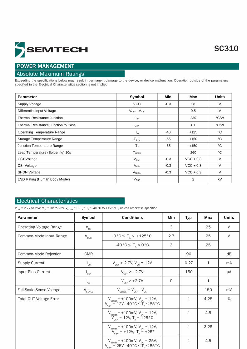
Absolute Maximum Ratings
Electrical Characteristics
Exceeding the specifications below may result in permanent damage to the device, or device malfunction. Operation outside of the parametersspecified in the Electrical Characteristics section is not implied.
VCS+ = 2.7V to 25V, VCC = 3V to 25V, VSENSE = 0, TA = TJ = -40°C to +125°C , unless otherwise specified
retemaraP retemaraP retemaraP retemaraP retemaraP lobmyS lobmyS lobmyS lobmyS lobmyS snoitidnoC snoitidnoC snoitidnoC snoitidnoC snoitidnoC niM niM niM niM niM pyT pyT pyT pyT pyT xaM xaM xaM xaM xaM stinU stinU stinU stinU stinU
egnaRegatloVgnitarepO V CC 3 52 V
egnaRtupnIedoM-nommoC V RMC C°0 ≤ TA ≤ C°521+ 7.2 52 V
C°04- ≤ TA C°0< 3 52
noitcejeRedoM-nommoC RMC 09 Bd
tnerruCylppuS I CC V +SC V,V7.2> CC V21= 72.0 1 Am
tnerruCsaiBtupnI I +SC V +SC V7.2+> 051 Aμ
I -SC V +SC V7.2+> 0 1
egatloVesneSelacS-lluF V ESNES V ESNES V= +SC V- -SC 051 Vm
rorrEegatloVTUOlatoT V ESNES V,Vm001+= CC ,V21=V +SC C°04-,V21= ≤ TA ≤ C°58
1 52.4 %
V ESNES V,Vm001+= CC ,V21=V +SC T,V21= A C°521=
1 5.4
V ESNES V,Vm001+= CC ,V21=V +SC T,V21+= A º52+=
1 52.3
V ESNES V,Vm001+= CC ,V52=V +SC C°04-,V52= ≤ TA ≤ C°58
1 5.4
Parameter Symbol Min Max Units
Supply Voltage VCC -0.3 28 V
Differential Input Voltage VCS+ - VCS- 0.5 V
Thermal Resistance Junction θJA 230 °C/W
Thermal Resistance Junction to Case θJC 81 °C/W
Operating Temperature Range TA -40 +125 °C
Storage Temperature Range TSTG -65 +150 °C
Junction Temperature Range TJ -65 +150 °C
Lead Temperature (Soldering) 10s TLEAD 260 °C
CS+ Voltage VCS+ -0.3 VCC + 0.3 V
CS- Voltage VCS- -0.3 VCC + 0.3 V
SHDN Voltage VSHDN -0.3 VCC + 0.3 V
ESD Rating (Human Body Model) VESD 2 kV
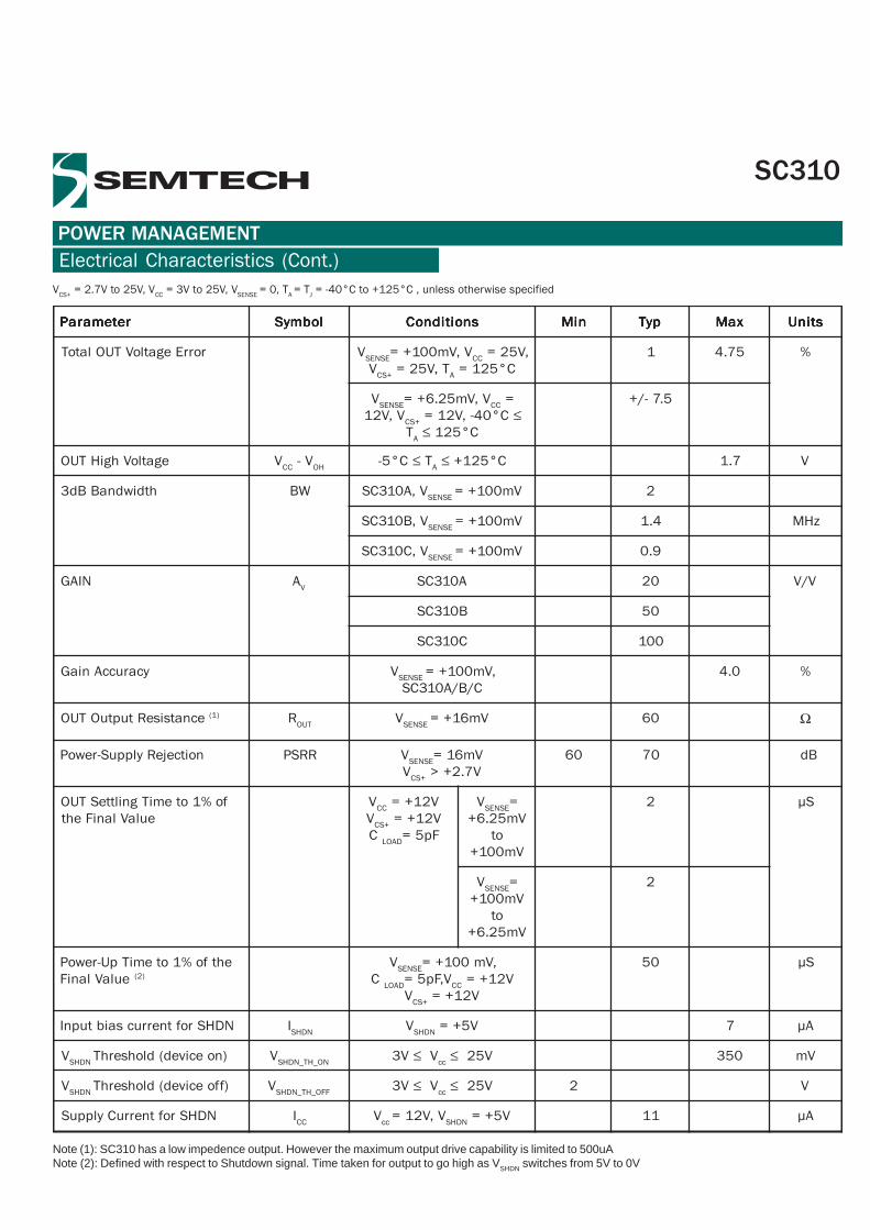
3© 2005 Semtech Corp. www.semtech.com
POWER MANAGEMENT
SC310
Electrical Characteristics (Cont.)
retemaraP retemaraP retemaraP retemaraP retemaraP lobmyS lobmyS lobmyS lobmyS lobmyS snoitidnoC snoitidnoC snoitidnoC snoitidnoC snoitidnoC niM niM niM niM niM pyT pyT pyT pyT pyT xaM xaM xaM xaM xaM stinU stinU stinU stinU stinU
rorrEegatloVTUOlatoT V ESNES V,Vm001+= CC ,V52=V +SC T,V52= A C°521=
1 57.4 %
V ESNES V,Vm52.6+= CC =V,V21 +SC C°04-,V21= ≤
TA ≤ C°521
5.7-/+
egatloVhgiHTUO V CC V- HO C°5- ≤ TA ≤ C°521+ 7.1 V
htdiwdnaBBd3 WB V,A013CS ESNES Vm001+= 2
V,B013CS ESNES Vm001+= 4.1 zHM
V,C013CS ESNES Vm001+= 9.0
NIAG AV A013CS 02 V/V
B013CS 05
C013CS 001
ycaruccAniaG V ESNES ,Vm001+=C/B/A013CS
0.4 %
ecnatsiseRtuptuOTUO )1( R TUO V ESNES Vm61+= 06 Ω
noitcejeRylppuS-rewoP RRSP V ESNES Vm61=V +SC V7.2+>
06 07 Bd
fo%1otemiTgniltteSTUOeulaVlaniFeht
V CC V21+=V +SC V21+=C DAOL Fp5=
V ESNES =Vm52.6+
otVm001+
2 Sμ
V ESNES =Vm001+
otVm52.6+
2
ehtfo%1otemiTpU-rewoPeulaVlaniF )2(
V ESNES ,Vm001+=C DAOL V,Fp5= CC V21+=
V +SC V21+=
05 Sμ
NDHSroftnerrucsaibtupnI I NDHS V NDHS V5+= 7 Aμ
V NDHS )noecived(dlohserhT V NO_HT_NDHS V3 ≤ V cc ≤ V52 053 Vm
V NDHS )ffoecived(dlohserhT V FFO_HT_NDHS V3 ≤ V cc ≤ V52 2 V
NDHSroftnerruCylppuS I CC V cc V,V21= NDHS V5+= 11 Aμ
Note (1): SC310 has a low impedence output. However the maximum output drive capability is limited to 500uANote (2): Defined with respect to Shutdown signal. Time taken for output to go high as VSHDN switches from 5V to 0V
VCS+ = 2.7V to 25V, VCC = 3V to 25V, VSENSE = 0, TA = TJ = -40°C to +125°C , unless otherwise specified
4 2005 Semtech Corp. www.semtech.com
POWER MANAGEMENT
SC310
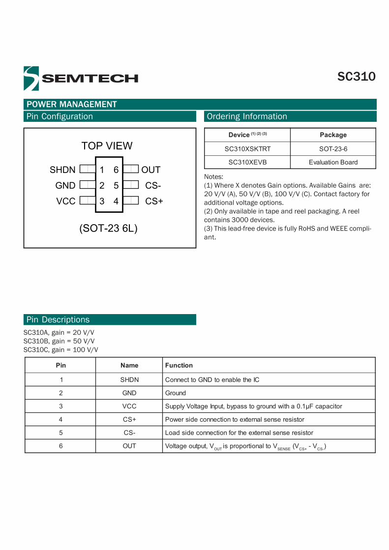
3
1SHDN
TOP VIEW
(SOT-23 6L)
5 CS-
VCC
6
CS+4
OUT
2GND
Pin Configuration Ordering Information
eciveD )3()2()1( egakcaP
TRTKSX013CS 6-32-TOS
BVEX013CS draoBnoitaulavE
Pin Descriptions
niP emaN noitcnuF
1 NDHS CIehtelbaneotDNGottcennoC
2 DNG dnuorG
3 CCV roticapacFµ1.0ahtiwdnuorgotssapyb,tupnIegatloVylppuS
4 +SC rotsiseresneslanretxeotnoitcennocedisrewoP
5 -SC rotsiseresneslanretxeehtrofnoitcennocedisdaoL
6 TUO V,tuptuoegatloV TUO Votlanoitroporpsi ESNES V( +SC V- -SC )
SC310A, gain = 20 V/VSC310B, gain = 50 V/VSC310C, gain = 100 V/V
Notes:(1) Where X denotes Gain options. Available Gains are:20 V/V (A), 50 V/V (B), 100 V/V (C). Contact factory foradditional voltage options.(2) Only available in tape and reel packaging. A reelcontains 3000 devices.(3) This lead-free device is fully RoHS and WEEE compli-ant.
5 2005 Semtech Corp. www.semtech.com
POWER MANAGEMENT
SC310
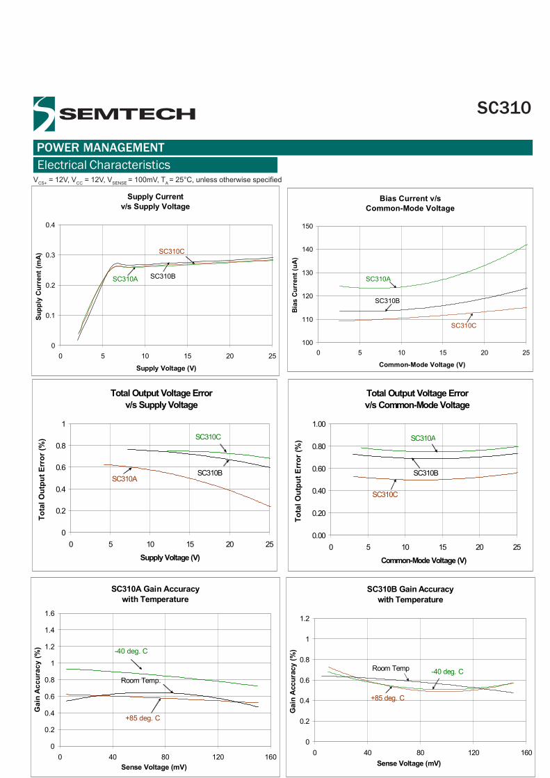
Electrical Characteristics
T
VCS+ = 12V, VCC = 12V, VSENSE = 100mV, TA = 25°C, unless otherwise specified
Supply Current v/s Supply Voltage
0
0.1
0.2
0.3
0.4
0 5 10 15 20 25
Supply Voltage (V)
Supp
ly C
urre
nt (m
A)
SC310BSC310A
SC310C
Bias Current v/s Common-Mode Voltage
100
110
120
130
140
150
0 5 10 15 20 25
Common-Mode Voltage (V)
Bia
s C
urre
nt (u
A)
SC310A
SC310B
SC310C
Total Output Voltage Error v/s Supply Voltage
0
0.2
0.4
0.6
0.8
1
0 5 10 15 20 25
Supply Voltage (V)
Tota
l Out
put E
rror
(%)
SC310ASC310B
SC310C
Total Output Voltage Error v/s Common-Mode Voltage
0.00
0.20
0.40
0.60
0.80
1.00
0 5 10 15 20 25
Common-Mode Voltage (V)
Tota
l Out
put E
rror
(%)
SC310C
SC310A
SC310B
SC310A Gain Accuracywith Temperature
0
0.2
0.4
0.6
0.8
1
1.2
1.4
1.6
0 40 80 120 160Sense Voltage (mV)
Gai
n A
ccur
acy
(%) -40 deg. C
+85 deg. C
Room Temp.
SC310B Gain Accuracywith Temperature
0
0.2
0.4
0.6
0.8
1
1.2
0 40 80 120 160Sense Voltage (mV)
Gai
n A
ccur
acy
(%)
Room Temp
+85 deg. C
-40 deg. C
6 2005 Semtech Corp. www.semtech.com
POWER MANAGEMENT
SC310
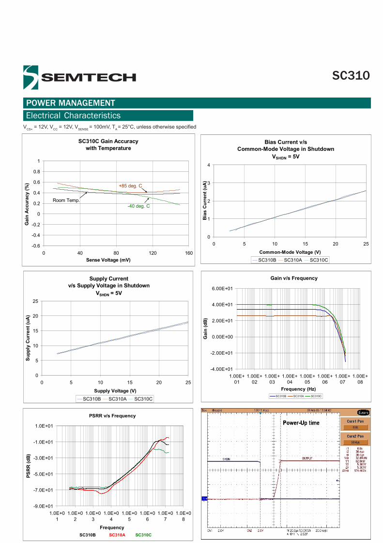
Electrical Characteristics
PSRR v/s Frequency
-9.0E+01
-7.0E+01
-5.0E+01
-3.0E+01
-1.0E+01
1.0E+01
1.0E+01
1.0E+02
1.0E+03
1.0E+04
1.0E+05
1.0E+06
1.0E+07
1.0E+08
Frequency
PSR
R (d
B)
SC310CSC310B SC310A
Gain v/s Frequency
-4.00E+01
-2.00E+01
0.00E+00
2.00E+01
4.00E+01
6.00E+01
1.00E+01
1.00E+02
1.00E+03
1.00E+04
1.00E+05
1.00E+06
1.00E+07
1.00E+08
Frequency (Hz)
Gai
n (d
B)
SC310B SC310A SC310C
VCS+ = 12V, VCC = 12V, VSENSE = 100mV, TA = 25°C, unless otherwise specified
SC310C Gain Accuracywith Temperature
-0.6
-0.4
-0.2
0
0.2
0.4
0.6
0.8
1
0 40 80 120 160Sense Voltage (mV)
Gai
n A
ccur
acy
(%)
-40 deg. CRoom Temp.
+85 deg. C
Bias Current v/s Common-Mode Voltage in Shutdown
VSHDN = 5V
0
1
2
3
4
0 5 10 15 20 25
Common-Mode Voltage (V)
Bia
s C
urre
nt (u
A)
SC310B SC310A SC310C
Supply Current v/s Supply Voltage in Shutdown
VSHDN = 5V
0
5
10
15
20
25
0 5 10 15 20 25
Supply Voltage (V)
Supp
ly C
urre
nt (u
A)
SC310B SC310A SC310C
7 2005 Semtech Corp. www.semtech.com
POWER MANAGEMENT
SC310
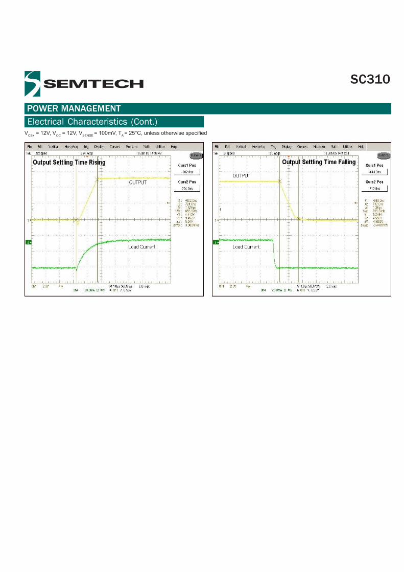
Electrical Characteristics (Cont.)VCS+ = 12V, VCC = 12V, VSENSE = 100mV, TA = 25°C, unless otherwise specified
8 2005 Semtech Corp. www.semtech.com
POWER MANAGEMENT
SC310
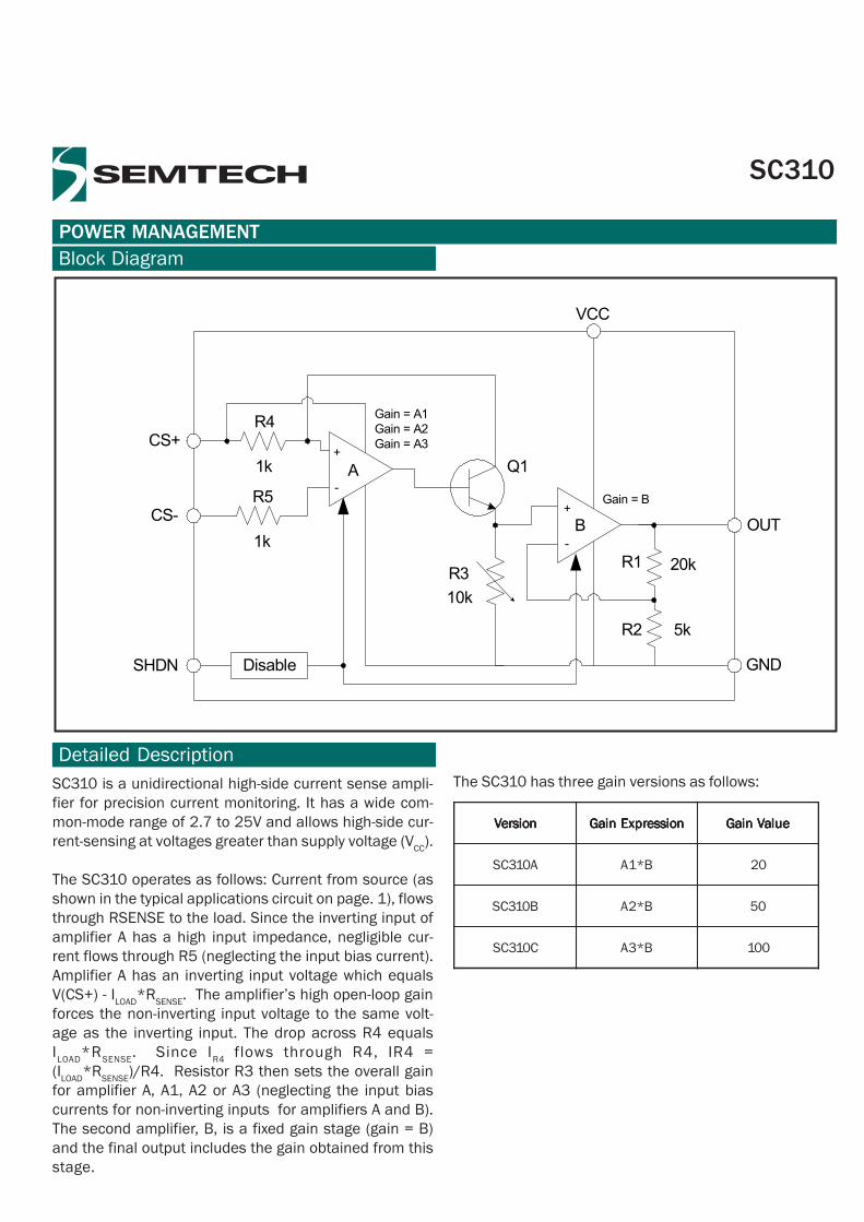
Block Diagram
Detailed DescriptionSC310 is a unidirectional high-side current sense ampli-fier for precision current monitoring. It has a wide com-mon-mode range of 2.7 to 25V and allows high-side cur-rent-sensing at voltages greater than supply voltage (VCC).
The SC310 operates as follows: Current from source (asshown in the typical applications circuit on page. 1), flowsthrough RSENSE to the load. Since the inverting input ofamplifier A has a high input impedance, negligible cur-rent flows through R5 (neglecting the input bias current).Amplifier A has an inverting input voltage which equalsV(CS+) - ILOAD*RSENSE. The amplifier’s high open-loop gainforces the non-inverting input voltage to the same volt-age as the inverting input. The drop across R4 equalsILOAD*RSENSE. Since IR4 flows through R4, IR4 =(ILOAD*RSENSE)/R4. Resistor R3 then sets the overall gainfor amplifier A, A1, A2 or A3 (neglecting the input biascurrents for non-inverting inputs for amplifiers A and B).The second amplifier, B, is a fixed gain stage (gain = B)and the final output includes the gain obtained from thisstage.
noisreV noisreV noisreV noisreV noisreV noisserpxEniaG noisserpxEniaG noisserpxEniaG noisserpxEniaG noisserpxEniaG eulaVniaG eulaVniaG eulaVniaG eulaVniaG eulaVniaG
A013CS B*1A 02
B013CS B*2A 05
C013CS B*3A 001
The SC310 has three gain versions as follows:
VCC
+
-
+
-R1
R2
R3
R4
R5
Q1A
B
Gain = A1Gain = A2Gain = A3
Gain = BCS-
GNDSHDN
CS+
OUT
1k
10k
20k
5k
1k
Disable
9 2005 Semtech Corp. www.semtech.com
POWER MANAGEMENT
SC310
PCB trace can also be used as the sense resistor. Thishas the drawback of significant error at the output overtemperature. The trade-off, despite the error in the out-put voltage, provides for a cost-effective solution.
SHDN FSHDN FSHDN FSHDN FSHDN Functionunctionunctionunctionunction
The SHDN pin should not be kept floating and must betied to either ground or be held high. Connecting the pinto ground is needed for normal operation. The voltagelevel at the SHDN pin is independent of the functioningof the IC.
TTTTTypical Vypical Vypical Vypical Vypical Values falues falues falues falues for Sense Ror Sense Ror Sense Ror Sense Ror Sense Resistesistesistesistesistorororororsssss
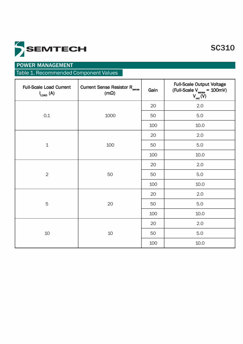
Table 1. lists the common resistor values for typical op-eration of the SC310. SC310 is capable of sensing wideranges of currents providing proper sense resistors areused.
Output ImpedanceOutput ImpedanceOutput ImpedanceOutput ImpedanceOutput Impedance
The output impedance of the SC310 is very low. Typicalvalue is 60Ω. Connecting the OUT pin to a high-imped-ance input stage is recommended. Resistive loading onthe OUT pin will not affect the gain of the SC310.
Common Mode InputCommon Mode InputCommon Mode InputCommon Mode InputCommon Mode Input
The sense voltage is limited at low values of common modeinput voltage (VCMR ). The figure below specifies the de-sired sense voltage for low common mode input volt-age. In the figure below we see that SC310A can be op-erated over full-scale sense voltage at Vcs+ = 2.7V,whereas the voltage is limited for SC310B and SC310C.
Layout GuidelinesLayout GuidelinesLayout GuidelinesLayout GuidelinesLayout Guidelines
1. Place the SC310 between the pins and external cir-cuitry to reduce the trace length.2. Place the decoupling capacitor at the input (VCC) asclose as possible to the pin.3. An R-C filter at the input will help achieve the highestnoise rejection.4. Run the traces from RSENSE as close as possible. Useminimum width traces to reduce capacitive coupling.
Choosing RChoosing RChoosing RChoosing RChoosing Rsensesensesensesensesense
Full scale sense voltage for the amplifier is 150mV max.The resistor (Rsense) is selected depending on the load ofthe system. For light loads a bigger value of Rsense is se-lected to minimize the error in the proportional outputvoltage. Higher resistor value improves the strength ofthe signal at the current-sense amplifier input and hencegives an accurate output.
The voltage at the OUT pin of the amplifier is given as:
Vout = (Gain) * (Iload) * (Rsense)
Similarly, for heavy loads, a smaller value of Rsense resis-tor is used not to exceed the max “Sense Voltage” ratingof the IC. Also at high loads, a power rating of Rsense re-sistor is used and must be acceptable (greater than I2Rpower dissipation in the resistor).
Application Information
Vsense
0 70mV 150mV
2.7V
3.5V
28VV C
S+
35mV
5V
SC310C SC310B
SC310A
Not drawn to scale
10 2005 Semtech Corp. www.semtech.com
POWER MANAGEMENT
SC310
tnerruCdaoLelacS-lluF tnerruCdaoLelacS-lluF tnerruCdaoLelacS-lluF tnerruCdaoLelacS-lluF tnerruCdaoLelacS-lluFIIIII DAOL DAOL DAOL DAOL DAOL )A( )A( )A( )A( )A(
RrotsiseResneStnerruC RrotsiseResneStnerruC RrotsiseResneStnerruC RrotsiseResneStnerruC RrotsiseResneStnerruC esnes esnes esnes esnes esnes
m(m(m(m(m( ΩΩΩΩΩ)))))niaG niaG niaG niaG niaG
egatloVtuptuOelacS-lluF egatloVtuptuOelacS-lluF egatloVtuptuOelacS-lluF egatloVtuptuOelacS-lluF egatloVtuptuOelacS-lluFVelacS-lluF( VelacS-lluF( VelacS-lluF( VelacS-lluF( VelacS-lluF( esnes esnes esnes esnes esnes )Vm001= )Vm001= )Vm001= )Vm001= )Vm001=
VVVVV tuo tuo tuo tuo tuo )V( )V( )V( )V( )V(
1.0 0001
02 0.2
05 0.5
001 0.01
1 001
02 0.2
05 0.5
001 0.01
2 05
02 0.2
05 0.5
001 0.01
5 02
02 0.2
05 0.5
001 0.01
01 01
02 0.2
05 0.5
001 0.01
Table 1. Recommended Component Values
11 2005 Semtech Corp. www.semtech.com
POWER MANAGEMENT
SC310
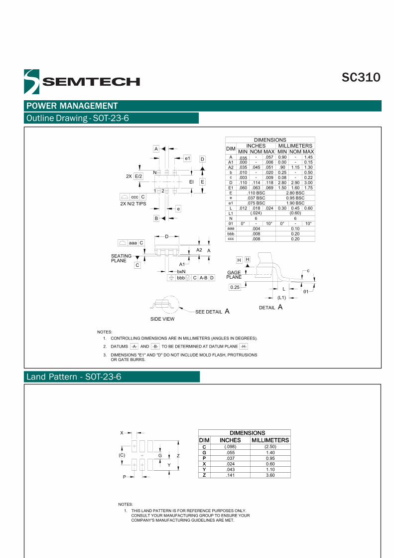
Outline Drawing - SOT-23-6
.110 BSC
.037 BSC
DETAIL
aaa C
SEATING
ccc C2X N/2 TIPS
2X E/2
6
SEE DETAIL
A1
AA2
bxN
A
.008
1 2
N
E.060
.114
.063.118
.010 -
6
A
0.20
1.603.00
2.80 BSC0.95 BSC
.069 1.502.90
.020 0.25
1.75
0.50-
EI
L
(L1)
c
010.25
PLANEGAGE
H
2.80.110
bbb C A-B D
0°
.008
-.004
.012
.003
(.024).018
-
.035
.000
.035--
.045
0.10
0.20
10° 0° - 10°
1.15
(0.60)0.45.024
.009
0.30
0.08
.057
.051
.006 0.00.90
0.90
0.22
0.60
-
0.151.45
1.30--
1.90 BSC.075 BSC
A
e1 D
e
B
CH
NOMINCHES
DIMENSIONS
L1
aaabbbccc
01N
DIM
c
ee1L
E1E
D
A1A2b
AMIN
MILLIMETERSMAX MIN NOM MAX
PLANE
D
DATUMS AND TO BE DETERMINED AT DATUM PLANE
CONTROLLING DIMENSIONS ARE IN MILLIMETERS (ANGLES IN DEGREES).
DIMENSIONS "E1" AND "D" DO NOT INCLUDE MOLD FLASH, PROTRUSIONS3.OR GATE BURRS.
NOTES:1.
2. -A- -B- -H-
SIDE VIEW
Land Pattern - SOT-23-6
THIS LAND PATTERN IS FOR REFERENCE PURPOSES ONLY.CONSULT YOUR MANUFACTURING GROUP TO ENSURE YOURCOMPANY'S MANUFACTURING GUIDELINES ARE MET.
NOTES:1.
DIMENSIONSINCHES
YZ
DIM
GPX
CMILLIMETERS
P
(C) Z
Y
G
.043
.141
.055(.098)
.037
.024
1.40(2.50)
0.950.601.103.60
X DIMENSIONSINCHES
YZ
DIM
GPX
CMILLIMETERS
12 2005 Semtech Corp. www.semtech.com
POWER MANAGEMENT
SC310
Table 1. Recommended Component Values
NOTES
Visit us at: www.semtech.com
Semtech CorporationPower Management Products Division200 Flynn Road, Camarillo, CA 93012
Phone: (805) 498-2111 FAX (805)498-3804
Contact Information