Embed Size (px)
Citation preview
SCAN926260
www.ti.com SNLS153H –JUNE 2002–REVISED APRIL 2013
SCAN926260 Six 1 to 10 Bus LVDS Deserializers with IEEE 1149.1 and At-Speed BISTCheck for Samples: SCAN926260
1FEATURES DESCRIPTIONThe SCAN926260 integrates six 10-bit deserializer
2• Deserializes One to Six Bus LVDS Input Serialdevices into a single chip. The SCAN926260 canData Streams with Embedded Clockssimultaneously deserialize up to six data streams that
• IEEE 1149.1 (JTAG) Compliant and At-Speed have been serialized by TI’s 10-bit Bus LVDSBIST Test Modes serializers. In addition, the SCAN926260 is compliant
with IEEE standard 1149.1 and also features an At-• Parallel Clock Rate 16-66MHzSpeed Built-In Self Test (BIST). For more details,• On Chip Filtering for PLLplease see the sections titled IEEE 1149.1 Test
• High Impedance Inputs Upon Power Off (Vcc = Modes and BIST Alone Test Modes.0V)
Each deserializer block in the SCAN926260 has it’s• Single Power Supply at +3.3V own powerdown pin (PWRDWN[n])and operates• 196-Pin NFBGA Package (Low-Profile Ball Grid independently with its own clock recovery circuitry
Array) Package and lock-detect signaling. In addition, a masterpowerdown pin (MS_PWRDWN) which puts all the• Industrial Temperature Range Operation:entire device into sleep mode is provided.−40°C to +85°CThe SCAN926260 uses a single +3.3V power supply• ROUTn[0:9] and RCLKn Default High whenand consumes 1.2W at 3.3V with a PRBS-15 patternChannel is Not Lockedon all channels at 660Mbps.• Powerdown Per Channel to Conserve Power
on Unused Channels
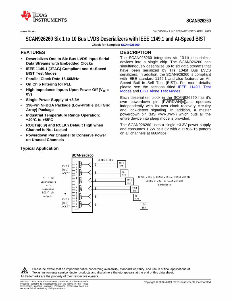
Typical Application
1
Please be aware that an important notice concerning availability, standard warranty, and use in critical applications ofTexas Instruments semiconductor products and disclaimers thereto appears at the end of this data sheet.
2All trademarks are the property of their respective owners.
PRODUCTION DATA information is current as of publication date. Copyright © 2002–2013, Texas Instruments IncorporatedProducts conform to specifications per the terms of the TexasInstruments standard warranty. Production processing does notnecessarily include testing of all parameters.
SCAN926260
SNLS153H –JUNE 2002–REVISED APRIL 2013 www.ti.com
These devices have limited built-in ESD protection. The leads should be shorted together or the device placed in conductive foamduring storage or handling to prevent electrostatic damage to the MOS gates.
Absolute Maximum Ratings (1) (2)
Supply Voltage (VDD) -0.3 to 3.8V
BLVDS Input Voltage (Rin ±) -0.3V to +3.9V
Maximum Package Power Dissipation Capacity @ 25°C 3.7W
θJA 196 NFBGA: 34°C/WPackage Thermal Resistance
θJC 196 NFBGA: 8°C/W
Storage Temp. Range -65°C to +150°C
Junction Temperature +125°C
Lead Temperature (Soldering 10 Seconds) +225°C
Human Body Model >2KVESD Ratings
Machine Model >250V
(1) Absolute Maximum Ratings are those values beyond which the safety of the device cannot be ensured. They are not meant to imply thatthe devices should be operated at these limits. The table of Electrical Characteristics specifies conditions of device operation.
(2) If Military/Aerospace specified devices are required, please contact the Texas Instruments Sales Office/ Distributors for availability andspecifications.
Recommended Operating ConditionsSupply Voltage (VDD) 3.0V to 3.6V
Operating Free Air Temperature (TA) -40°C to +85°C
Electrical CharacteristicsOver recommended operating supply and temperature ranges unless otherwise specified. (1)
Symbol Parameter Conditions Pin/Freq. Min Typ Max Units
LVCMOS/LVTTL DC Specifications
High Level InputVIH 2.0 VCC VVoltageREN, REFCLK,Low Level InputVIL GND 0.8 VPWRDWNn ,VoltageMS_PWRDWN
VCL Input Clamp Voltage -0.87 -1.5 V
IIN Input Current Vin = 0 or 3.6V -10 +10 uA
TRST, TMS, TDI,IIN Input Current Vin = 0 or 3.6V -20 +20 uABIST_SEL[0:2]
High Level OutputVOH IOH = −6mA 2 3 VCC VVoltage
Low Level OutputVOL IOL = 6mA GND 0.18 0.5 VVoltage ROUT,RCLK,Output short CircuitIOS Vout = 0V -15 -46 -85 mALOCKnCurrent
MS_PWRDWN orTri-state OutputIOZ REN = 0.8V -10 ±0.2 +10 µACurrent Vout = 0V or VCC
High Level OutputVOH IOH = −12mA 2 VCC VVoltage
Low Level OutputVOL IOL = 12mA TDO GND 0.5 VVoltage
Tri-state OutputIOS Vout = 0V -15 -120 mACurrent
(1) Typical values are given for VDD = 3.3V and TA =25°C
2 Submit Documentation Feedback Copyright © 2002–2013, Texas Instruments Incorporated
Product Folder Links: SCAN926260
SCAN926260
www.ti.com SNLS153H –JUNE 2002–REVISED APRIL 2013
Electrical Characteristics (continued)Over recommended operating supply and temperature ranges unless otherwise specified.(1)
Symbol Parameter Conditions Pin/Freq. Min Typ Max Units
Bus LVDS DC specifications
Differential ThresholdVTH +3 +50 mVVCM = 0.025,High Voltage1.250, 2.375V
Differential Threshold (VRI+-VRI-)VTL -50mV -2 mVLow VoltageRI+, RI-
IIN Vin = +2.4V, -10 ±1 +10 µAVcc = 3.6 or 0VInput Current
Vin =0V, -10 ±1 +10 µAVcc = 3.6 or 0V
Supply Current
Checker BoardPattern, 66 MHz 500 600 mACL=15pFICCR Total Supply Current
PRBS-15 Pattern, 66 MHz 385 mACL=15pF
Reduction in Supply Checker BoardΔICCR 66 MHz 55 77 100 mACurrent per Channel Pattern
Total Supply Current MS_PWRDN=ICCXR 1.5 2.2 mAwhen Powered Down 0.8V (2)
Timing Requirements for REFCLK
tRFCP REFCLK Period 15.15 62.5 ns
tRFDC REFCLK Duty Cycle 30 50 70 %
Ratio of REFCLK totRFCP/tTCP 0.95 1.05TCLK
REFCLK TransitiontRFTT 8 nsTime
Deserializer Switching Characteristics
tRCP RCLK Period 15.15 62.5 nsRCLK
tRDC RCLK Duty Cycle See (3) 41 50 55 %
LVCMOS/LVTTL Low-tCLH 1.3 1.8 2.2 nsto-High Transition Time CL = 15pF,Figure 3 (4)
LVCMOS/LVTTL High-tCHL 1.0 1.5 2.0 nsto-Low Transition Time
Rout Data Valid beforetROS See Figure 2 0.4*tRCP nsRCLK LOCK,RCLK,Rout Data Valid aftertROH See Figure 2 -0.4*tRCP nsROUTRCLK
tHZR High to Tri-state Delay 10 ns
tLZR Low to Tri-state Delay 10 nsSee Figure 7
tZHR Tri-state to High Delay 12 ns
tZLR Tri-state to Low Delay 12 ns
See Figure 1 1.75*tRCP+5 1.75*tRCP+7 1.75*tRCP+10 ns(All Cases)tDD Deserializer Delay RCLK66 MHz Only 1.75*tRCP+6 1.75*tRCP+7 1.75*tRCP+9 ns
(2) Total Supply Current when Powered Down (ICCXR) is higher than previous six channel devices because previous devices assertedROUTn and RCLKn into tri-state upon loss-of-lock, whereas the SCAN926260 now asserts ROUTn and RCLKn HIGH upon loss-of-lock.
(3) tRDC was specified by measuring the positive pulse on the RCLK and dividing this number by the ideal pulse width.(4) tCLH and tCHL are Ensured by Statistical Analysis (EBSA). Please see Figure 3 for a graphical representation.
Copyright © 2002–2013, Texas Instruments Incorporated Submit Documentation Feedback 3
Product Folder Links: SCAN926260
SCAN926260
SNLS153H –JUNE 2002–REVISED APRIL 2013 www.ti.com
Electrical Characteristics (continued)Over recommended operating supply and temperature ranges unless otherwise specified.(1)
Symbol Parameter Conditions Pin/Freq. Min Typ Max Units
Deserializer PLL LOCK 66MHz 2.5 µstDSR1 Time from PWRDNn See Figure 4 (5)
16MHz 7.0 µs(with SYNCPAT)
66MHz 1.1 µsDeserializer PLL LocktDSR2 See Figure 5 (5)Time from SYNCPAT 16MHz 4.5 µs
66MHz 400 500 psDeserializer RighttRNMI-RIGHT Noise Margin 16MHz 1.3 2.51 nsSee Figure 8 (6)
66MHz 440 600 psDeserializer Left NoisetRNMI-LEFT Margin 16MHz 1.4 2.59 ns
(5) For the purpose of specifying deserializer PLL performance, tDSR1 and tDSR2 are specified with the REFCLK running and stable, andspecific conditions of the incoming data stream (SYNCPATs). tDSR1 is the time required for the deserializer to indicate lock upon power-up or when leaving the power-down mode. tDSR2 is the time required to indicate lock for the powered-up and enabled deserializer whenthe input (RI+ and RI−) conditions change from not receiving data to receiving synchronization patterns (SYNCPATs). The time to lockto random data is dependent upon the incoming data and is not specified.
(6) tRNMI-LEFT and tRNMI-RIGHT are a measure of how much phase noise (jitter) the deserializer can tolerate in the incoming data streambefore bit errors occur. The Deserializer noise margin specification does not include transmitter jitter and is Ensured By StatisticalAnalysis (EBSA). Please see Figure 8 for a graphical representation.
SCAN Circuitry Timing RequirementsSymbol Parameter Conditions Min Typ Max Units
fMAX Maximum TCK Clock RL = 500Ω, CL = 35 pF 25.0 50.0 MHzFrequency
tS TDI to TCK, H or L 2.0 ns
tH TDI to TCK, H or L 1.0 ns
tS TMS to TCK, H or L 2.5 ns
tH TMS to TCK, H or L 1.0 ns
tW TCK Pulse Width, H or L 10.0 ns
tW TRST Pulse Width, L 2.5 ns
tREC Recovery Time, TRST to 2.0 nsTCK
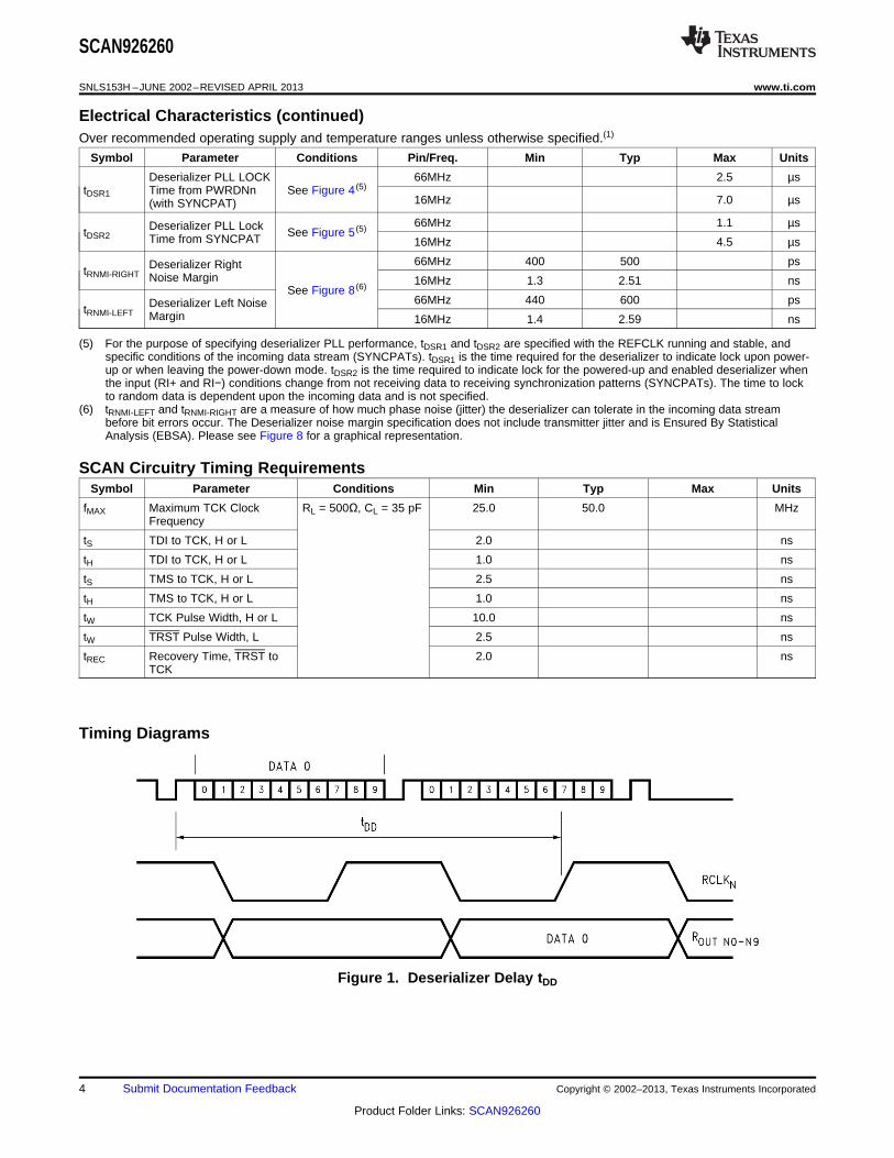
Timing Diagrams
Figure 1. Deserializer Delay tDD
4 Submit Documentation Feedback Copyright © 2002–2013, Texas Instruments Incorporated
Product Folder Links: SCAN926260
SCAN926260
www.ti.com SNLS153H –JUNE 2002–REVISED APRIL 2013
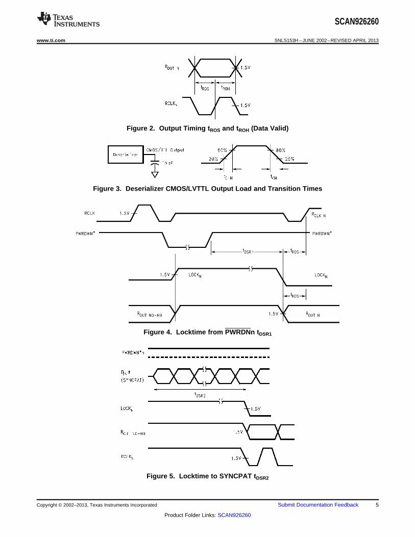
Figure 2. Output Timing tROS and tROH (Data Valid)
Figure 3. Deserializer CMOS/LVTTL Output Load and Transition Times
Figure 4. Locktime from PWRDNn tDSR1
Figure 5. Locktime to SYNCPAT tDSR2
Copyright © 2002–2013, Texas Instruments Incorporated Submit Documentation Feedback 5
Product Folder Links: SCAN926260
SCAN926260
SNLS153H –JUNE 2002–REVISED APRIL 2013 www.ti.com
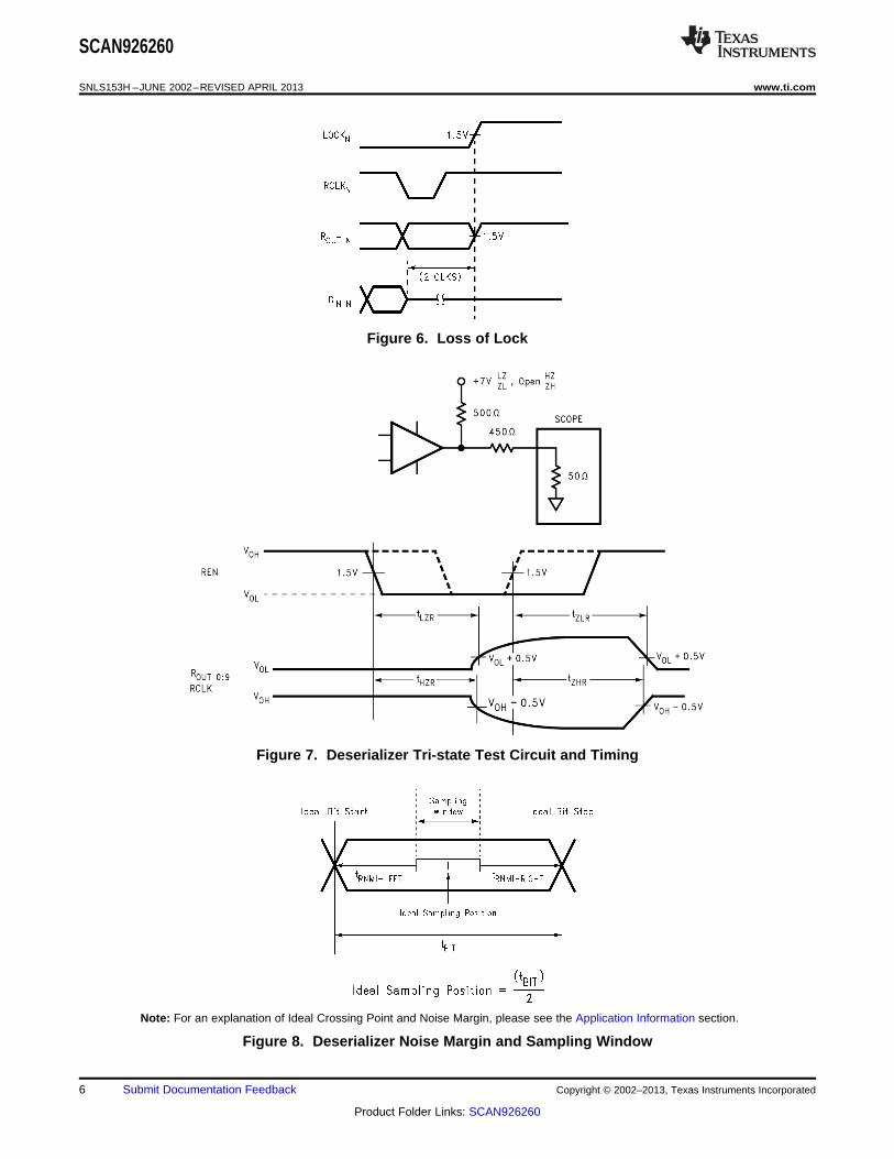
Figure 6. Loss of Lock
Figure 7. Deserializer Tri-state Test Circuit and Timing
Note: For an explanation of Ideal Crossing Point and Noise Margin, please see the Application Information section.
Figure 8. Deserializer Noise Margin and Sampling Window
6 Submit Documentation Feedback Copyright © 2002–2013, Texas Instruments Incorporated
Product Folder Links: SCAN926260
SCAN926260
www.ti.com SNLS153H –JUNE 2002–REVISED APRIL 2013
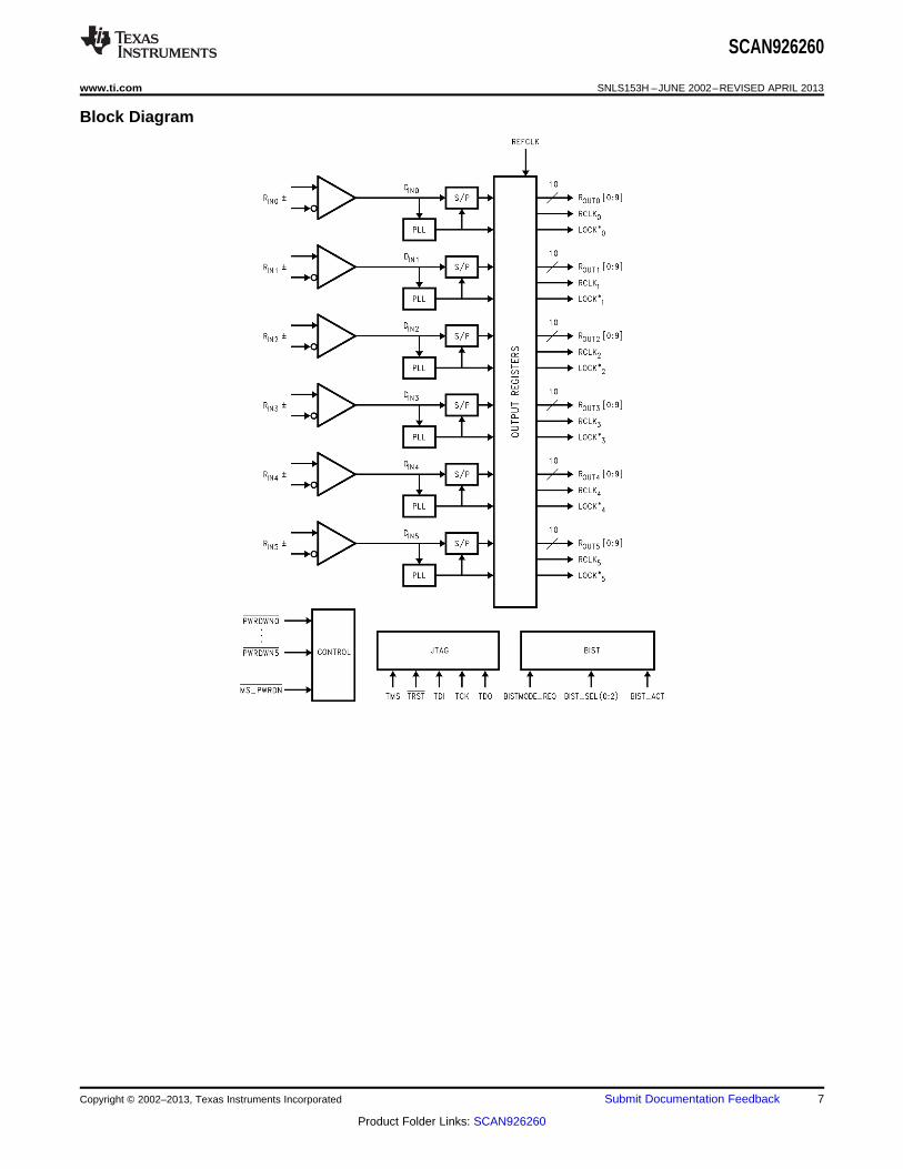
Block Diagram
Copyright © 2002–2013, Texas Instruments Incorporated Submit Documentation Feedback 7
Product Folder Links: SCAN926260
SCAN926260
SNLS153H –JUNE 2002–REVISED APRIL 2013 www.ti.com
Functional Description
The SCAN926260 combines six 1:10 deserializers into a single chip. Each of the six deserializers accepts a BusLVDS data stream from TI's DS92LV1021, DS92LV1023, DS92LV8028, SCAN921023, or SCAN921025Serializer. The deserializers then recover the clock and data to deliver the resulting 10-bit wide words to theoutputs.
Each of the six channels acts completely independent of each other. Each independent channel has outputs fora 10-bit wide data word, a recovered clock output, and a lock-detect output.
The SCAN926260 has three operating states: Initialization, Data Transfer, and Resynchronization. In addition,there are two passive states: Powerdown and Tri-state. During normal operation, the SCAN6260 also has thecapability of utilizing the IEEE 1149.1 test modes (JTAG) or the Built-In Self Test mode (BIST).
The following sections describe each operating mode, passive states, and the JTAG and BIST modes.
Initialization
Before the SCAN926260 receives and deserializes data, it and the transmitting Serializer must initialize the link.Initialization refers to synchronizing the Serializer's and the Deserializer's PLL's to local clocks. The local clocksmust be within ±5% of the incoming transmitter clock frequency. After all devices synchronize to local clocks, theDeserializer synchronizes to the Serializer as the second and final initialization step.
Step 1: After applying power to the Deserializer, the outputs are held high and the on-chip Power-on Reset(POR) circuitry disables the internal circuits. When Vcc reaches VccOK (2.1V), the PLL in each deserializer beginslocking to the local clock (REFCLK). A local on-board oscillator or other source that provides the specified clockinput to the REFCLK pin.
Step 2: The Deserializer PLL must synchronize to the Serializer to complete the initialization. Refer to theSerializer data sheet for proper operation during the Initialization State. The Deserializer identifies the rising clockedge in a synchronization pattern or pseudo-random data and after 80 clock cycles will synchronize to the datastream from the Serializer. At the point where the Deserializer's PLL locks to the embedded clock, the LOCKnpin goes low and valid data appears at the outputs.
Data Transfer
After initialization, the Serializer transfers data to the Deserializer. The serial data stream includes a start andstop bit appended by the serializer, which frames the ten data bits. The start bit is always high and the stop bit isalways low. The start and stop bits also function as clock bits embedded in the serial stream.
The Serializer transmits the data and clock bits (10+2 bits) at 12 times the TCLK frequency. For example, ifTCLK is 40 MHz, the serial rate is 40 X 12 = 480 Mbps. Since only 10 bits are from input data, the serial'payload' rate is 10 times the TCLK frequency. For instance, if TCLK = 40 MHz, the payload data is 40 X 10 =400 Mbps. TCLK is provided by the data source and must be in the range of 16MHz to 66MHz.
When one of six Deserializer channels synchronizes to the input from a Serializer, it drives its LOCKn pin lowand synchronously delivers valid data at its outputs. The Deserializer locks to the embedded clock, uses it togenerate multiple internal data strobes, and drives the embedded clock to the RCLKn pin. The RCLKn pin issynchronous to the data on the ROUTn[0:9] pins. While LOCKn is low, data on ROUTn[0:9] is valid. Otherwise,ROUTn[0:9] and RCLKn are high.
All ROUT, LOCK, and RCLK signals will drive a minimum of three CMOS input gates (15pF load) with a 66 MHzclock. This amount of drive allows bussing outputs of two Deserializers and a destination ASIC. REN controls tri-state of all the outputs.
The Deserializer input pins are high impedance during Powerdown (PWRDNn or MS_PWRDN low) and power-off (Vcc = 0V).
Resynchronization
Whenever one of the six Deserializers loses lock, it will automatically try to resynchronize. For example, if theembedded clock edge is not detected two times in succession, the PLL loses lock and the LOCKn pin is drivenhigh. The system must monitor the LOCKn pin to determine when data is valid.
8 Submit Documentation Feedback Copyright © 2002–2013, Texas Instruments Incorporated
Product Folder Links: SCAN926260
SCAN926260
www.ti.com SNLS153H –JUNE 2002–REVISED APRIL 2013
The user has the choice of allowing the deserializer to re-sync to the data stream or to force synchronization byasserting the Serializer SYNC1 or SYNC2 pin high. This scheme is left up to user discretion. Onerecommendation is to provide a feedback loop using the LOCKn pin itself to control the sync request of theSerializer (SYNC1 or SYNC2). Dual SYNC pins are provided for local or remote control..
Powerdown
The Powerdown state is a low power sleep mode that the Deserializer typically occupies while waiting forinitialization or to reduce power consumption when no data is transferred. While in Powerdown Mode, the PLLstops and RCLK and ROUTn[0:9] are high, which reduces the supply current for each channel by approximately80mA. Each channel has a powerdown (PWRDWNn) pin that puts the respective channel into sleep mode whenasserted low. In addition, the SCAN926260 has a master powerdown (MS_PWRDWN) pin that overrides eachindividual powerdown pin and puts the entire device into sleep mode when asserted low (This same conditioncan be replicated by asserting all six individual powerdown pins low.). The powerdown pins are internally pulledlow which defaults the device into sleep mode. Active operation requires asserting a high on MS_PWRDWN andthe selected channel’s PWRDWNn pin.
Upon exiting Powerdown, the Deserializer enters the Initialization state. The system must then allow time toInitialize before data transfer can begin.
Tri-state
When the system drives the REN pin low, the Deserializer enters tri-state. This will tri-state the receiver outputpins (ROUTn[0:9]) and RCLK[0:5]. When the system drives REN high, the Deserializer will return to the previousstate as long as all other control pins remain static (PWRDWNn, MS_PWRDWN). The LOCKn pin is not affectedby REN and continues to be active, signalling LOCK status. This allows the system to be sure the channel islocked before enabling the data outputs.
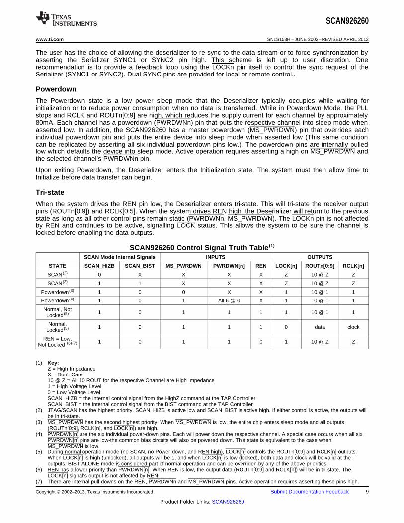
SCAN926260 Control Signal Truth Table (1)
SCAN Mode Internal Signals INPUTS OUTPUTS
STATE SCAN_HIZB SCAN_BIST MS_PWRDWN PWRDWN[n] REN LOCK[n] ROUTn[0:9] RCLK[n]
SCAN (2) 0 X X X X Z 10 @ Z Z
SCAN (2) 1 1 X X X Z 10 @ Z Z
Powerdown (3) 1 0 0 X X 1 10 @ 1 1
Powerdown (4) 1 0 1 All 6 @ 0 X 1 10 @ 1 1
Normal, Not 1 0 1 1 1 1 10 @ 1 1Locked (5)
Normal, 1 0 1 1 1 0 data clockLocked (5)
REN = Low, 1 0 1 1 0 1 10 @ Z ZNot Locked (6) (7)
(1) Key:Z = High ImpedanceX = Don’t Care10 @ Z = All 10 ROUT for the respective Channel are High Impedance1 = High Voltage Level0 = Low Voltage LevelSCAN_HIZB = the internal control signal from the HighZ command at the TAP ControllerSCAN_BIST = the internal control signal from the BIST command at the TAP Controller
(2) JTAG/SCAN has the highest priority. SCAN_HIZB is active low and SCAN_BIST is active high. If either control is active, the outputs willbe in tri-state.
(3) MS_PWRDWN has the second highest priority. When MS_PWRDWN is low, the entire chip enters sleep mode and all outputs(ROUTn[0:9], RCLK[n], and LOCK[n]) are high.
(4) PWRDWN[n] are the six individual power-down pins. Each will power down the respective channel. A special case occurs when all sixPWRDWN[n] pins are low-the common bias circuits will also be powered down. This state is equivalent to the case whenMS_PWRDWN is low.
(5) During normal operation mode (no SCAN, no Power-down, and REN high), LOCK[n] controls the ROUTn[0:9] and RCLK[n] outputs.When LOCK[n] is high (unlocked), all outputs will be 1, and when LOCK[n] is low (locked), both data and clock will be valid at theoutputs. BIST-ALONE mode is considered part of normal operation and can be overriden by any of the above priorities.
(6) REN has a lower priority than PWRDWN[n]. When REN is low, the output data (ROUTn[0:9] and RCLK[n]) will be in tri-state. TheLOCK[n] signal’s output is not affected by REN.
(7) There are internal pull-downs on the REN, PWRDWNn and MS_PWRDWN pins. Active operation requires asserting these pins high.
Copyright © 2002–2013, Texas Instruments Incorporated Submit Documentation Feedback 9
Product Folder Links: SCAN926260
SCAN926260
SNLS153H –JUNE 2002–REVISED APRIL 2013 www.ti.com
SCAN926260 Control Signal Truth Table(1) (continued)SCAN Mode Internal Signals INPUTS OUTPUTS
STATE SCAN_HIZB SCAN_BIST MS_PWRDWN PWRDWN[n] REN LOCK[n] ROUTn[0:9] RCLK[n]
REN = Low, 1 0 1 1 0 0 10 @ Z ZLocked (6) (7)
Default State (7) 0 0 0 1 10 @ 1 1
IEEE 1149.1 Test Modes
The SCAN926260 features interconnect test access that is compliant to the IEEE 1149.1 Standard for BoundaryScan Test (JTAG). All digital TTL I/O's on the device are accessible using IEEE 1149.1, and entering this testmode will override all input control cases including power down and REN. In addition to the four required TestAccess Port (TAP) signals of TMS, TCK, TDI, and TDO, TRST is provided for test reset.
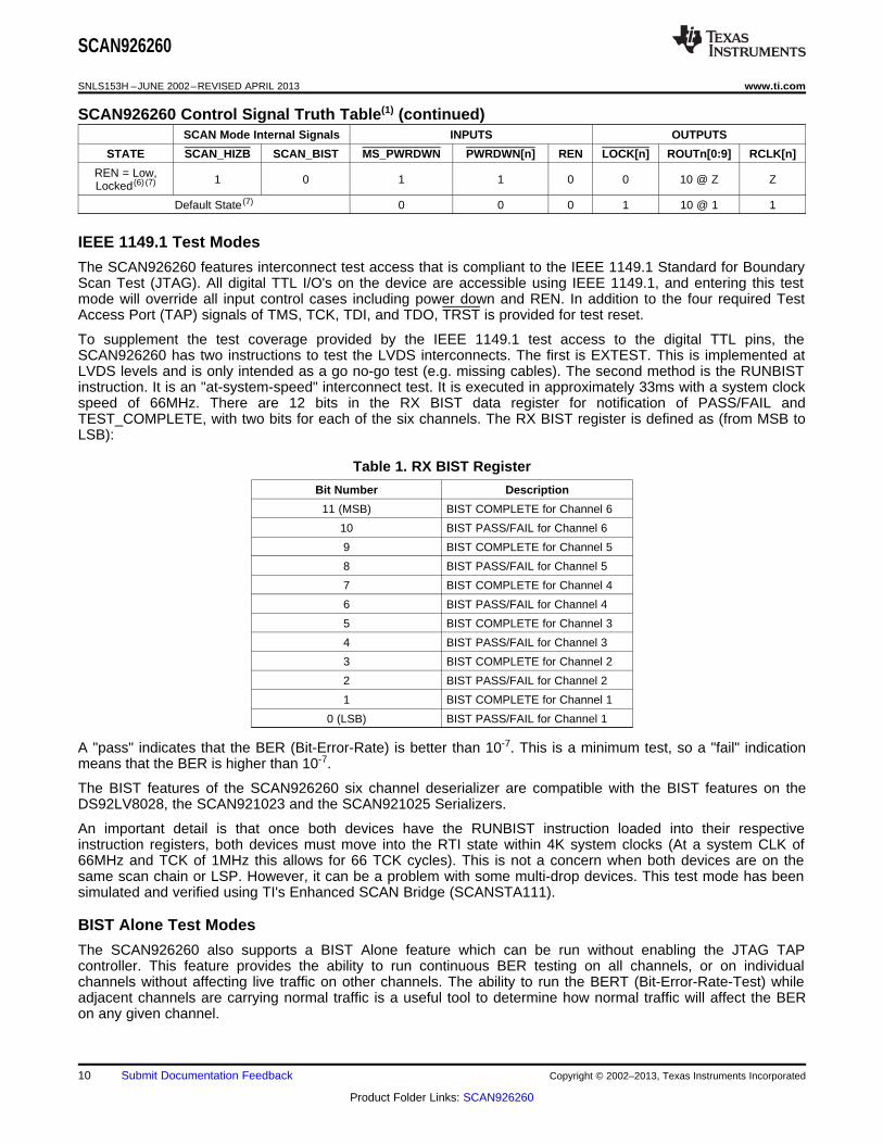
To supplement the test coverage provided by the IEEE 1149.1 test access to the digital TTL pins, theSCAN926260 has two instructions to test the LVDS interconnects. The first is EXTEST. This is implemented atLVDS levels and is only intended as a go no-go test (e.g. missing cables). The second method is the RUNBISTinstruction. It is an "at-system-speed" interconnect test. It is executed in approximately 33ms with a system clockspeed of 66MHz. There are 12 bits in the RX BIST data register for notification of PASS/FAIL andTEST_COMPLETE, with two bits for each of the six channels. The RX BIST register is defined as (from MSB toLSB):
Table 1. RX BIST Register
Bit Number Description
11 (MSB) BIST COMPLETE for Channel 6
10 BIST PASS/FAIL for Channel 6
9 BIST COMPLETE for Channel 5
8 BIST PASS/FAIL for Channel 5
7 BIST COMPLETE for Channel 4
6 BIST PASS/FAIL for Channel 4
5 BIST COMPLETE for Channel 3
4 BIST PASS/FAIL for Channel 3
3 BIST COMPLETE for Channel 2
2 BIST PASS/FAIL for Channel 2
1 BIST COMPLETE for Channel 1
0 (LSB) BIST PASS/FAIL for Channel 1
A "pass" indicates that the BER (Bit-Error-Rate) is better than 10-7. This is a minimum test, so a "fail" indicationmeans that the BER is higher than 10-7.
The BIST features of the SCAN926260 six channel deserializer are compatible with the BIST features on theDS92LV8028, the SCAN921023 and the SCAN921025 Serializers.
An important detail is that once both devices have the RUNBIST instruction loaded into their respectiveinstruction registers, both devices must move into the RTI state within 4K system clocks (At a system CLK of66MHz and TCK of 1MHz this allows for 66 TCK cycles). This is not a concern when both devices are on thesame scan chain or LSP. However, it can be a problem with some multi-drop devices. This test mode has beensimulated and verified using TI's Enhanced SCAN Bridge (SCANSTA111).
BIST Alone Test Modes
The SCAN926260 also supports a BIST Alone feature which can be run without enabling the JTAG TAPcontroller. This feature provides the ability to run continuous BER testing on all channels, or on individualchannels without affecting live traffic on other channels. The ability to run the BERT (Bit-Error-Rate-Test) whileadjacent channels are carrying normal traffic is a useful tool to determine how normal traffic will affect the BERon any given channel.
10 Submit Documentation Feedback Copyright © 2002–2013, Texas Instruments Incorporated
Product Folder Links: SCAN926260
SCAN926260
www.ti.com SNLS153H –JUNE 2002–REVISED APRIL 2013
The BIST Alone features can be accessed using the 5 pins defined as BIST_SEL0, BIST_SEL1, BIST_SEL2,BIST_ACT, and BISTMODE_REQ.
BIST_ACT activates the BIST Alone mode. The BIST Alone mode will continue until deactivated by theBIST_ACT pin. The BIST_ACT input must be high or low for four or more clock cycles in order to activate ordeactivate the BIST Alone mode. The BIST_ACT input is pulled low internally.
BISTMODE_REQ is used to select either gross error reporting or a specific output error report. When the BISTAlone mode is active, the LOCKn output for all channels running BIST Alone will go low and the respectiveROUTn(0:9) output will report any errors. When BISTMODE_REQ is low, the error reporting is set to GrossMode, and whenever a bit contains one or more errors, ROUT(0:9) for that channel goes high and stays highuntil deactivation by the BIST_ACT input. When BISTMODE_REQ is high, the output error reporting is set to BitError mode. Whenever any data bit contains an error, the data output for that corresponding bit goes high. Thedefault setting is Gross Error mode.
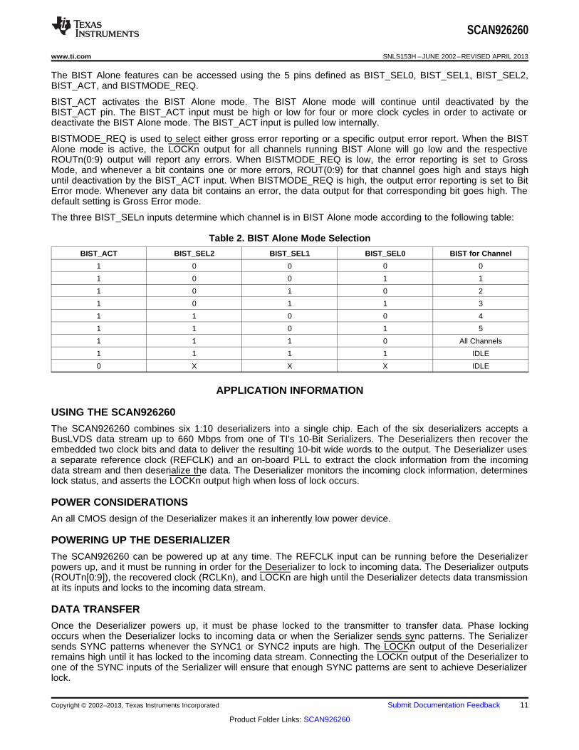
The three BIST_SELn inputs determine which channel is in BIST Alone mode according to the following table:
Table 2. BIST Alone Mode Selection
BIST_ACT BIST_SEL2 BIST_SEL1 BIST_SEL0 BIST for Channel
1 0 0 0 0
1 0 0 1 1
1 0 1 0 2
1 0 1 1 3
1 1 0 0 4
1 1 0 1 5
1 1 1 0 All Channels
1 1 1 1 IDLE
0 X X X IDLE
APPLICATION INFORMATION
USING THE SCAN926260
The SCAN926260 combines six 1:10 deserializers into a single chip. Each of the six deserializers accepts aBusLVDS data stream up to 660 Mbps from one of TI's 10-Bit Serializers. The Deserializers then recover theembedded two clock bits and data to deliver the resulting 10-bit wide words to the output. The Deserializer usesa separate reference clock (REFCLK) and an on-board PLL to extract the clock information from the incomingdata stream and then deserialize the data. The Deserializer monitors the incoming clock information, determineslock status, and asserts the LOCKn output high when loss of lock occurs.
POWER CONSIDERATIONS
An all CMOS design of the Deserializer makes it an inherently low power device.
POWERING UP THE DESERIALIZER
The SCAN926260 can be powered up at any time. The REFCLK input can be running before the Deserializerpowers up, and it must be running in order for the Deserializer to lock to incoming data. The Deserializer outputs(ROUTn[0:9]), the recovered clock (RCLKn), and LOCKn are high until the Deserializer detects data transmissionat its inputs and locks to the incoming data stream.
DATA TRANSFER
Once the Deserializer powers up, it must be phase locked to the transmitter to transfer data. Phase lockingoccurs when the Deserializer locks to incoming data or when the Serializer sends sync patterns. The Serializersends SYNC patterns whenever the SYNC1 or SYNC2 inputs are high. The LOCKn output of the Deserializerremains high until it has locked to the incoming data stream. Connecting the LOCKn output of the Deserializer toone of the SYNC inputs of the Serializer will ensure that enough SYNC patterns are sent to achieve Deserializerlock.
Copyright © 2002–2013, Texas Instruments Incorporated Submit Documentation Feedback 11
Product Folder Links: SCAN926260
SCAN926260
SNLS153H –JUNE 2002–REVISED APRIL 2013 www.ti.com
The Deserializer can also lock to incoming data by simply powering up the device and allowing the “lock topseudo random data” circuitry to find and lock to the data stream.
While the Deserializer LOCKn output is low, data at the respective channel’s Deserializer outputs (ROUTn[0:9])is valid, except for the specific case when loss of lock occurs during transmission which is further discussed inthe RECOVERING FROM LOCK LOSS section below.
NOISE MARGIN
The Deserializer noise margin is the amount of input jitter (phase noise) that the Deserializer can tolerate and stillreliably receive data. Various environmental and systematic factors include:
Serializer: TCLK jitter, VDD noise (noise bandwidth and out-of-band noise)
Media: ISI, Large VCM shifts
Deserializer: VDD noise
Please see the section on USING NOISE MARGIN TO VALIDATE SIGNAL QUALITY for more information.
RECOVERING FROM LOCK LOSS
In the case where the Deserializer loses lock during data transmission, up to 1 cycle of data that was previouslyreceived can be invalid. This is due to the delay in the lock detection circuit. The lock detect circuit requires thatinvalid clock information be received two times in a row to indicate loss of lock. Since clock information has beenlost, it is possible that data was also lost during these cycles. Therefore, after the Deserializer relocks to theincoming data stream and the Deserializer LOCKn pin goes low, at least one previous data cycle should besuspect for bit errors.
The Deserializer can relock to the incoming data stream by making the Serializer resend SYNC patterns, asdescribed above, or by locking to pseudo random data, which can take more time, depending on the datapatterns being received.
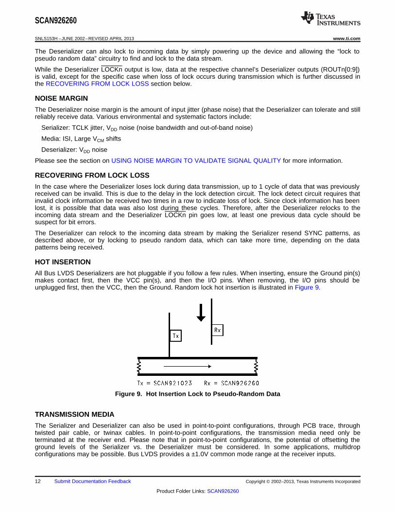
HOT INSERTION
All Bus LVDS Deserializers are hot pluggable if you follow a few rules. When inserting, ensure the Ground pin(s)makes contact first, then the VCC pin(s), and then the I/O pins. When removing, the I/O pins should beunplugged first, then the VCC, then the Ground. Random lock hot insertion is illustrated in Figure 9.
Figure 9. Hot Insertion Lock to Pseudo-Random Data
TRANSMISSION MEDIA
The Serializer and Deserializer can also be used in point-to-point configurations, through PCB trace, throughtwisted pair cable, or twinax cables. In point-to-point configurations, the transmission media need only beterminated at the receiver end. Please note that in point-to-point configurations, the potential of offsetting theground levels of the Serializer vs. the Deserializer must be considered. In some applications, multidropconfigurations may be possible. Bus LVDS provides a ±1.0V common mode range at the receiver inputs.
12 Submit Documentation Feedback Copyright © 2002–2013, Texas Instruments Incorporated
Product Folder Links: SCAN926260
SCAN926260
www.ti.com SNLS153H –JUNE 2002–REVISED APRIL 2013
FAILSAFE BIASING FOR THE SCAN926260
The SCAN926260 has internal failsafe biasing and an improved input threshold sensitivity of ±50mV versus±100mV for the DS92LV1210.. This allows for a greater differential noise margin. However, in cases where thereceiver input is not being actively driven, the increased sensitivity of the SCAN926260 can pickup noise as asignal and cause unintentional locking. For example, this can occur when an input cable is disconnected.
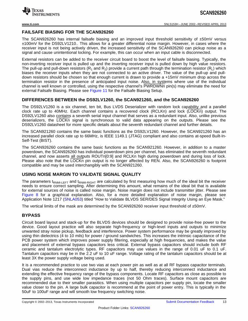
External resistors can be added to the receiver circuit board to boost the level of failsafe biasing. Typically, thenon-inverting receiver input is pulled up and the inverting receiver input is pulled down by high value resistors.The pull-up and pull-down resistors (R1 and R2) provide a current path through the termination resistor (RL) whichbiases the receiver inputs when they are not connected to an active driver. The value of the pull-up and pull-down resistors should be chosen so that enough current is drawn to provide a +15mV minimum drop across thetermination resistor in the presence of anticipated input noise. Also, in systems where use of the individualchannel is well known or controlled, using the respective channel’s PWRDWNn pin(s) may eliminate the need forexternal Failsafe Biasing. Please see Figure 11 for the Failsafe Biasing Setup.
DIFFERENCES BETWEEN the DS92LV1260, the SCAN921260, and the SCAN926260
The DS92LV1260 is a six channel, ten bit, Bus LVDS Deserializer with random lock capability and a parallelclock rate up to 40MHz. Each channel contains a recovered clock (RCLKn) and lock (LOCKn) output. TheDS92LV1260 also contains a seventh serial input channel that serves as a redundant input. Also, unlike previousdeserializers, the LOCKn signal is synchronous to valid data appearing on the outputs. Please see theDS92LV1260 datasheet for more specific details about the seventh redundant channel and further details.
The SCAN921260 contains the same basic functions as the DS92LV1260. However, the SCAN921260 has anincreased parallel clock rate up to 66MHz, is IEEE 1149.1 (JTAG) compliant and also contains at-speed Built-In-Self-Test (BIST).
The SCAN926260 contains the same basic functions as the SCAN921260. However, in addition to a masterpowerdown, the SCAN926260 has individual powerdown pins per channel, has eliminated the seventh redundantchannel, and now asserts all outputs ROUTn[0:9] and RCLKn high during powerdown and during loss of lock.Please also note that the LOCKn pin output is no longer affected by REN. Also, the SCAN926260 is footprintcompatible and may be used interchangibly with the SCAN921260.
USING NOISE MARGIN TO VALIDATE SIGNAL QUALITY
The parameters tRNMI-LEFT and tRNMI-RIGHT are calculated by first measuring how much of the ideal bit the receiverneeds to ensure correct sampling. After determining this amount, what remains of the ideal bit that is availablefor external sources of noise is called noise margin. Noise margin does not include transmitter jitter. Please seeFigure 8 for a graphical explanation. Also, for a more detailed explanation of noise margin, please seeApplication Note 1217 (SNLA053) titled "How to Validate BLVDS SER/DES Signal Integrity Using an Eye Mask."
The vertical limits of the mask are determined by the SCAN926260 receiver input threshold of ±50mV.
BYPASS
Circuit board layout and stack-up for the BLVDS devices should be designed to provide noise-free power to thedevice. Good layout practice will also separate high-frequency or high-level inputs and outputs to minimizeunwanted stray noise pickup, feedback and interference. Power system performance may be greatly improved byusing thin dielectrics (4 to 10 mils) for power / ground sandwiches. This increases the intrinsic capacitance of thePCB power system which improves power supply filtering, especially at high frequencies, and makes the valueand placement of external bypass capacitors less critical. External bypass capacitors should include both RFceramic and tantalum electrolytic types. RF capacitors may use values in the range of 0.01 uF to 0.1 uF.Tantalum capacitors may be in the 2.2 uF to 10 uF range. Voltage rating of the tantalum capacitors should be atleast 3X the power supply voltage being used.
It is a recommended practice to use two vias at each power pin as well as at all RF bypass capacitor terminals.Dual vias reduce the interconnect inductance by up to half, thereby reducing interconnect inductance andextending the effective frequency range of the bypass components. Locate RF capacitors as close as possible tothe supply pins, and use wide low impedance traces (not 50 Ohm traces). Surface mount capacitors arerecommended due to their smaller parasitics. When using multiple capacitors per supply pin, locate the smallervalue closer to the pin. A large bulk capacitor is recommend at the point of power entry. This is typically in the50uF to 100uF range and will smooth low frequency switching noise.
Copyright © 2002–2013, Texas Instruments Incorporated Submit Documentation Feedback 13
Product Folder Links: SCAN926260
SCAN926260
SNLS153H –JUNE 2002–REVISED APRIL 2013 www.ti.com
Some devices provide separate power and ground pins for different portions of the circuit. This is done to isolateswitching noise effects between different sections of the circuit. Separate planes on the PCB are typically notrequired. Pin Description tables typically provide guidance on which circuit blocks are connected to which powerpin pairs. In some cases, an external filter may be used to provide clean power to sensitive circuits such as PLLcircuitry.
Use at least a four layer board with a power and ground plane. Locate CMOS (TTL) signals away from the LVDSlines to prevent coupling. Closely-coupled differential lines of 100 Ohms ZDIFF are typically recommended forLVDS interconnects. The closely-coupled lines help to ensure that coupled noise will appear as common-modeand is rejected by the receivers. Also, the tight coupled lines will radiate less.
Termination of the LVDS interconnect is required. For point-to-point applications, termination should be located atthe load end. Nominal value is 100 Ohms to match the line's differential impedance. Place the resistor as closeto the receiver inputs as possible to minimize the resulting stub between the termination resistor and receiver.
Additional general guidance can be found in the LVDS Owner's Manual - available in PDF format from the TIweb site at: http://www.ti.com/ww/en/analog/interface/lvds.shtml. For packaging information on NFBGA's, pleasesee AN-1126 (SNOA021).
Guidance for the SCAN926260 is provided next:
SCAN926260: SIX 1 TO 10 DESERIALIZERS
General guidance is provided below. Exact guidance can not be given as it is dictated by other board level/system level criteria. This includes the density of the board, power rails, power supply, and other integratedcircuit power supply needs.
DVDD = DIGITAL SECTION POWER SUPPLY
These pins supply the digital portion and receiver output buffers of the device. Receiver DVDD pins require morebypass to power outputs under synchronous switching conditions. An estimate of local capacitance requires aminimum of 20nF. This is calculated by taking 66 (60 LVTTL Outputs + 6 RCLK Outputs) times the maximumoutput short circuit current (IOS) of 85mA. Multiplying this number by the maximum rise time (tCLH) of 4ns anddividing by the maximum allowed droop in VDD (assume 50mV) yields 448.8nF. Dividing this number by thenumber of DVDD pins (25) yields 18nF. Rounding up to a standard value, 0.1uF is selected for each DVDD pin.The capacitative bandwidth for this capacitor may be extended by placing a 0.01uF capacitor in parallel. The0.01uF capacitor should be placed closer to the DVDD pin than the 0.1uF capacitor.
PVDD = PLL SECTION POWER SUPPLY
The PVDD pin supplies the PLL circuit. PLL circuits require clean power for the minimization of jitter. A supplynoise frequency in the 300kHZ to 1MHz range can cause increased output jitter. Certain power supplies mayhave switching frequencies or high harmonic content in this range. If this is the case, filtering of this noisespectrum may be required. A notch filter response is best to provide a stable VDD, suppression of the noiseband, and good high-frequency response (clock fundamental). This may be accomplished with a pie filter (CRCor CLC). If employed, a separate pie filter is recommended for each PLL to minimize drop in potential due to theseries resistance. Separate power planes for the PVDD pins is typically not required.
AVDD = LVDS SECTION POWER SUPPLY
The AVDD pin supplies the LVDS portion of the circuit. The SCAN926260 has four AVDD pins. Due to the natureof the design, current draw is not excessive on these pins. A 0.1uF capacitor is sufficient for these pins. If spaceis available, the 0.01uF capacitor may be used in parallel with the 0.1uF capacitor for additional high frequencyfiltering.
GROUNDs
The AGND pin should be connected to the signal common in the cable for the return path of any common-modecurrent. Most of the LVDS current will be odd-mode and return within the interconnect pair. A small amount ofcurrent may be even-mode due to coupled noise and driver imbalances. This current should return via a lowimpedance known path.
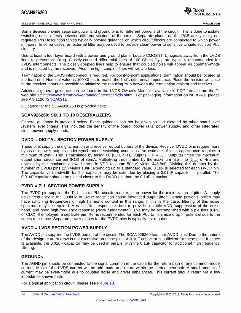
For a typical application circuit, please see Figure 10.
14 Submit Documentation Feedback Copyright © 2002–2013, Texas Instruments Incorporated
Product Folder Links: SCAN926260
0.01uF 0.1uF
RL
BLVDS Link
(Serializer AGND)
(Optional)
0.3uF 0.1uF 1.0uH 0.1uF
0.1uF 0.01uF
+Vcc
+Vcc
+Vcc
+
- +RINn
AGND
PVDD
PGND
DVDD
DGND
AVDD
SCAN926260(16-66 MHz)
Serializers:
DS92LV1021 (16-40 MHz)or
DS92LV1023 (40-66 MHz)or
DS92LV8028 (25-66 MHz)or
SCAN921023 (20-66 MHz)
orSCAN921025 (20-80
MHz)
SCAN926260
www.ti.com SNLS153H –JUNE 2002–REVISED APRIL 2013
(Only one power/ground for each supply type shown for clarity-bypass networks should be repeated for allpower/ground pairs.)
Figure 10. Typical Application Circuit
Figure 11. Optional Additional External Failsafe Biasing
Copyright © 2002–2013, Texas Instruments Incorporated Submit Documentation Feedback 15
Product Folder Links: SCAN926260
SCAN926260
SNLS153H –JUNE 2002–REVISED APRIL 2013 www.ti.com
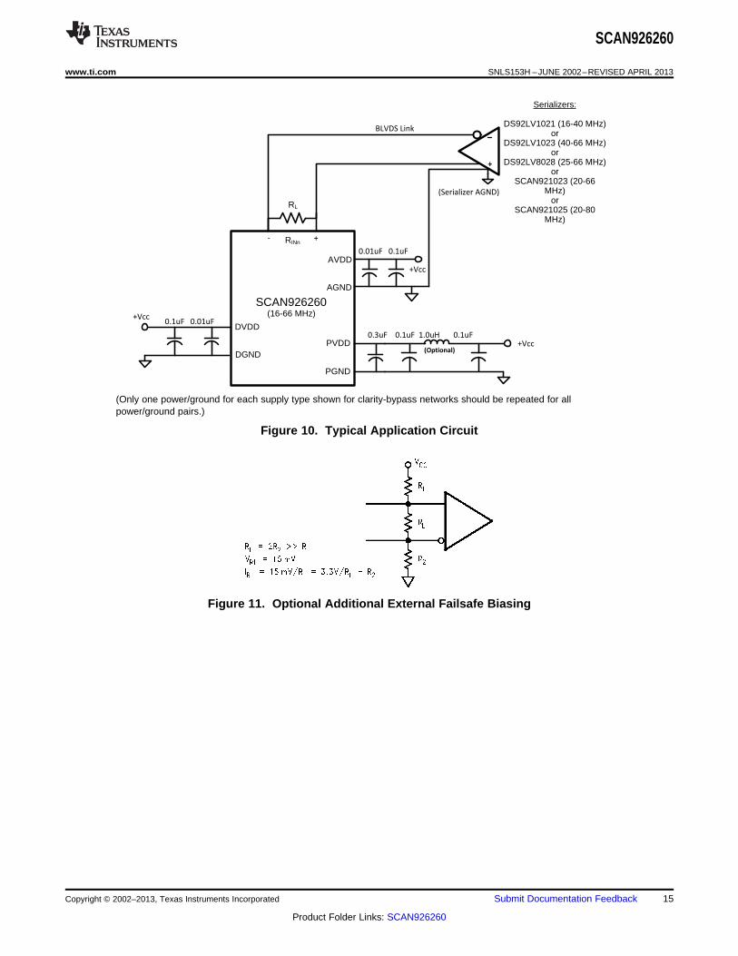
Pin Diagram
Figure 12. Top View of SCAN926260TUF (196 pin NFBGA)
Note: * = OVERBAR
16 Submit Documentation Feedback Copyright © 2002–2013, Texas Instruments Incorporated
Product Folder Links: SCAN926260
SCAN926260
www.ti.com SNLS153H –JUNE 2002–REVISED APRIL 2013
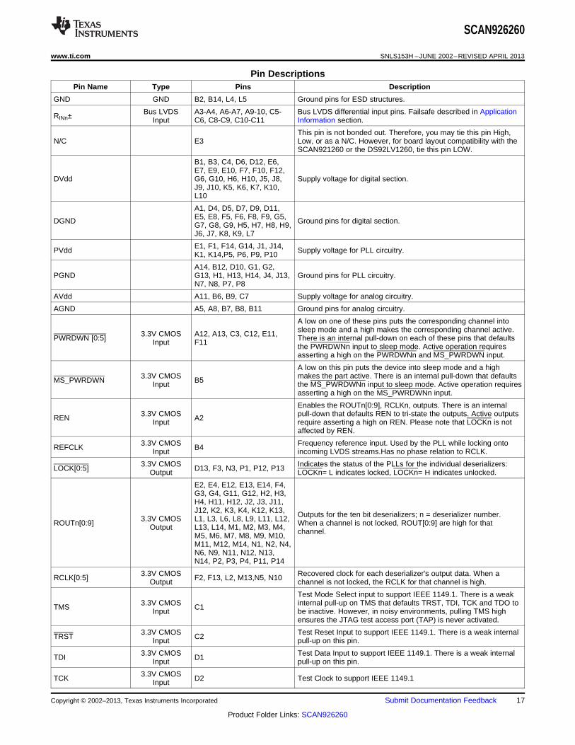
Pin DescriptionsPin Name Type Pins Description
GND GND B2, B14, L4, L5 Ground pins for ESD structures.
Bus LVDS A3-A4, A6-A7, A9-10, C5- Bus LVDS differential input pins. Failsafe described in ApplicationRINn± Input C6, C8-C9, C10-C11 Information section.
This pin is not bonded out. Therefore, you may tie this pin High,N/C E3 Low, or as a N/C. However, for board layout compatibility with the
SCAN921260 or the DS92LV1260, tie this pin LOW.
B1, B3, C4, D6, D12, E6,E7, E9, E10, F7, F10, F12,
DVdd G6, G10, H6, H10, J5, J8, Supply voltage for digital section.J9, J10, K5, K6, K7, K10,L10
A1, D4, D5, D7, D9, D11,E5, E8, F5, F6, F8, F9, G5,DGND Ground pins for digital section.G7, G8, G9, H5, H7, H8, H9,J6, J7, K8, K9, L7
E1, F1, F14, G14, J1, J14,PVdd Supply voltage for PLL circuitry.K1, K14,P5, P6, P9, P10
A14, B12, D10, G1, G2,PGND G13, H1, H13, H14, J4, J13, Ground pins for PLL circuitry.
N7, N8, P7, P8
AVdd A11, B6, B9, C7 Supply voltage for analog circuitry.
AGND A5, A8, B7, B8, B11 Ground pins for analog circuitry.
A low on one of these pins puts the corresponding channel intosleep mode and a high makes the corresponding channel active.3.3V CMOS A12, A13, C3, C12, E11,PWRDWN [0:5] There is an internal pull-down on each of these pins that defaultsInput F11 the PWRDWNn input to sleep mode. Active operation requiresasserting a high on the PWRDWNn and MS_PWRDWN input.
A low on this pin puts the device into sleep mode and a high3.3V CMOS makes the part active. There is an internal pull-down that defaultsMS_PWRDWN B5Input the MS_PWRDWNn input to sleep mode. Active operation requires
asserting a high on the MS_PWRDWNn input.
Enables the ROUTn[0:9], RCLKn, outputs. There is an internal3.3V CMOS pull-down that defaults REN to tri-state the outputs. Active outputsREN A2Input require asserting a high on REN. Please note that LOCKn is not
affected by REN.
3.3V CMOS Frequency reference input. Used by the PLL while locking ontoREFCLK B4Input incoming LVDS streams.Has no phase relation to RCLK.
3.3V CMOS Indicates the status of the PLLs for the individual deserializers:LOCK[0:5] D13, F3, N3, P1, P12, P13Output LOCKn= L indicates locked, LOCKn= H indicates unlocked.
E2, E4, E12, E13, E14, F4,G3, G4, G11, G12, H2, H3,H4, H11, H12, J2, J3, J11,J12, K2, K3, K4, K12, K13, Outputs for the ten bit deserializers; n = deserializer number.3.3V CMOS L1, L3, L6, L8, L9, L11, L12,ROUTn[0:9] When a channel is not locked, ROUT[0:9] are high for thatOutput L13, L14, M1, M2, M3, M4, channel.M5, M6, M7, M8, M9, M10,M11, M12, M14, N1, N2, N4,N6, N9, N11, N12, N13,N14, P2, P3, P4, P11, P14
3.3V CMOS Recovered clock for each deserializer's output data. When aRCLK[0:5] F2, F13, L2, M13,N5, N10Output channel is not locked, the RCLK for that channel is high.
Test Mode Select input to support IEEE 1149.1. There is a weak3.3V CMOS internal pull-up on TMS that defaults TRST, TDI, TCK and TDO toTMS C1Input be inactive. However, in noisy environments, pulling TMS high
ensures the JTAG test access port (TAP) is never activated.
3.3V CMOS Test Reset Input to support IEEE 1149.1. There is a weak internalTRST C2Input pull-up on this pin.
3.3V CMOS Test Data Input to support IEEE 1149.1. There is a weak internalTDI D1Input pull-up on this pin.
3.3V CMOSTCK D2 Test Clock to support IEEE 1149.1Input
Copyright © 2002–2013, Texas Instruments Incorporated Submit Documentation Feedback 17
Product Folder Links: SCAN926260
SCAN926260
SNLS153H –JUNE 2002–REVISED APRIL 2013 www.ti.com
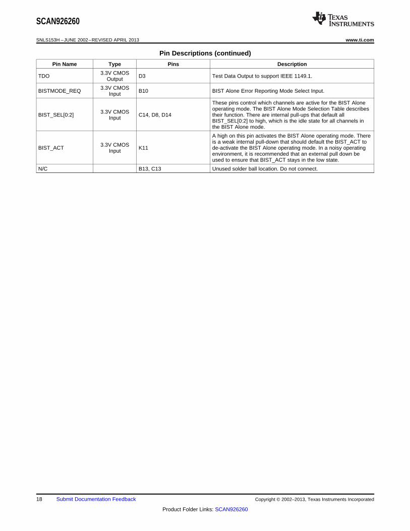
Pin Descriptions (continued)
Pin Name Type Pins Description
3.3V CMOSTDO D3 Test Data Output to support IEEE 1149.1.Output
3.3V CMOSBISTMODE_REQ B10 BIST Alone Error Reporting Mode Select Input.Input
These pins control which channels are active for the BIST Aloneoperating mode. The BIST Alone Mode Selection Table describes3.3V CMOSBIST_SEL[0:2] C14, D8, D14 their function. There are internal pull-ups that default allInput BIST_SEL[0:2] to high, which is the idle state for all channels inthe BIST Alone mode.
A high on this pin activates the BIST Alone operating mode. Thereis a weak internal pull-down that should default the BIST_ACT to3.3V CMOSBIST_ACT K11 de-activate the BIST Alone operating mode. In a noisy operatingInput environment, it is recommended that an external pull down beused to ensure that BIST_ACT stays in the low state.
N/C B13, C13 Unused solder ball location. Do not connect.
18 Submit Documentation Feedback Copyright © 2002–2013, Texas Instruments Incorporated
Product Folder Links: SCAN926260
SCAN926260
www.ti.com SNLS153H –JUNE 2002–REVISED APRIL 2013
REVISION HISTORY
Changes from Revision G (April 2013) to Revision H Page
• Changed layout of National Data Sheet to TI format .......................................................................................................... 18
Copyright © 2002–2013, Texas Instruments Incorporated Submit Documentation Feedback 19
Product Folder Links: SCAN926260
PACKAGE OPTION ADDENDUM
www.ti.com 4-Nov-2016
Addendum-Page 1
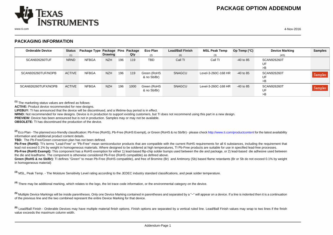
PACKAGING INFORMATION
Orderable Device Status(1)
Package Type PackageDrawing
Pins PackageQty
Eco Plan(2)
Lead/Ball Finish(6)
MSL Peak Temp(3)
Op Temp (°C) Device Marking(4/5)
Samples
SCAN926260TUF NRND NFBGA NZH 196 119 TBD Call TI Call TI -40 to 85 SCAN926260TUF>B
SCAN926260TUF/NOPB ACTIVE NFBGA NZH 196 119 Green (RoHS& no Sb/Br)
SNAGCU Level-3-260C-168 HR -40 to 85 SCAN926260TUF>B
SCAN926260TUFX/NOPB ACTIVE NFBGA NZH 196 1000 Green (RoHS& no Sb/Br)
SNAGCU Level-3-260C-168 HR -40 to 85 SCAN926260TUF>B
(1) The marketing status values are defined as follows:ACTIVE: Product device recommended for new designs.LIFEBUY: TI has announced that the device will be discontinued, and a lifetime-buy period is in effect.NRND: Not recommended for new designs. Device is in production to support existing customers, but TI does not recommend using this part in a new design.PREVIEW: Device has been announced but is not in production. Samples may or may not be available.OBSOLETE: TI has discontinued the production of the device.
(2) Eco Plan - The planned eco-friendly classification: Pb-Free (RoHS), Pb-Free (RoHS Exempt), or Green (RoHS & no Sb/Br) - please check http://www.ti.com/productcontent for the latest availabilityinformation and additional product content details.TBD: The Pb-Free/Green conversion plan has not been defined.Pb-Free (RoHS): TI's terms "Lead-Free" or "Pb-Free" mean semiconductor products that are compatible with the current RoHS requirements for all 6 substances, including the requirement thatlead not exceed 0.1% by weight in homogeneous materials. Where designed to be soldered at high temperatures, TI Pb-Free products are suitable for use in specified lead-free processes.Pb-Free (RoHS Exempt): This component has a RoHS exemption for either 1) lead-based flip-chip solder bumps used between the die and package, or 2) lead-based die adhesive used betweenthe die and leadframe. The component is otherwise considered Pb-Free (RoHS compatible) as defined above.Green (RoHS & no Sb/Br): TI defines "Green" to mean Pb-Free (RoHS compatible), and free of Bromine (Br) and Antimony (Sb) based flame retardants (Br or Sb do not exceed 0.1% by weightin homogeneous material)
(3) MSL, Peak Temp. - The Moisture Sensitivity Level rating according to the JEDEC industry standard classifications, and peak solder temperature.
(4) There may be additional marking, which relates to the logo, the lot trace code information, or the environmental category on the device.
(5) Multiple Device Markings will be inside parentheses. Only one Device Marking contained in parentheses and separated by a "~" will appear on a device. If a line is indented then it is a continuationof the previous line and the two combined represent the entire Device Marking for that device.
(6) Lead/Ball Finish - Orderable Devices may have multiple material finish options. Finish options are separated by a vertical ruled line. Lead/Ball Finish values may wrap to two lines if the finishvalue exceeds the maximum column width.
PACKAGE OPTION ADDENDUM
www.ti.com 4-Nov-2016
Addendum-Page 2
Important Information and Disclaimer:The information provided on this page represents TI's knowledge and belief as of the date that it is provided. TI bases its knowledge and belief on informationprovided by third parties, and makes no representation or warranty as to the accuracy of such information. Efforts are underway to better integrate information from third parties. TI has taken andcontinues to take reasonable steps to provide representative and accurate information but may not have conducted destructive testing or chemical analysis on incoming materials and chemicals.TI and TI suppliers consider certain information to be proprietary, and thus CAS numbers and other limited information may not be available for release.
In no event shall TI's liability arising out of such information exceed the total purchase price of the TI part(s) at issue in this document sold by TI to Customer on an annual basis.
TAPE AND REEL INFORMATION
*All dimensions are nominal
Device PackageType
PackageDrawing
Pins SPQ ReelDiameter
(mm)
ReelWidth
W1 (mm)
A0(mm)
B0(mm)
K0(mm)
P1(mm)
W(mm)
Pin1Quadrant
SCAN926260TUFX/NOPB NFBGA NZH 196 1000 330.0 24.4 15.3 15.3 2.5 20.0 24.0 Q1
PACKAGE MATERIALS INFORMATION
www.ti.com 10-Aug-2016
Pack Materials-Page 1
*All dimensions are nominal
Device Package Type Package Drawing Pins SPQ Length (mm) Width (mm) Height (mm)
SCAN926260TUFX/NOPB NFBGA NZH 196 1000 367.0 367.0 45.0
PACKAGE MATERIALS INFORMATION
www.ti.com 10-Aug-2016
Pack Materials-Page 2
MECHANICAL DATA
NZH0196A
www.ti.com
UJB196A (Rev C)
IMPORTANT NOTICE
Texas Instruments Incorporated and its subsidiaries (TI) reserve the right to make corrections, enhancements, improvements and otherchanges to its semiconductor products and services per JESD46, latest issue, and to discontinue any product or service per JESD48, latestissue. Buyers should obtain the latest relevant information before placing orders and should verify that such information is current andcomplete. All semiconductor products (also referred to herein as “components”) are sold subject to TI’s terms and conditions of salesupplied at the time of order acknowledgment.TI warrants performance of its components to the specifications applicable at the time of sale, in accordance with the warranty in TI’s termsand conditions of sale of semiconductor products. Testing and other quality control techniques are used to the extent TI deems necessaryto support this warranty. Except where mandated by applicable law, testing of all parameters of each component is not necessarilyperformed.TI assumes no liability for applications assistance or the design of Buyers’ products. Buyers are responsible for their products andapplications using TI components. To minimize the risks associated with Buyers’ products and applications, Buyers should provideadequate design and operating safeguards.TI does not warrant or represent that any license, either express or implied, is granted under any patent right, copyright, mask work right, orother intellectual property right relating to any combination, machine, or process in which TI components or services are used. Informationpublished by TI regarding third-party products or services does not constitute a license to use such products or services or a warranty orendorsement thereof. Use of such information may require a license from a third party under the patents or other intellectual property of thethird party, or a license from TI under the patents or other intellectual property of TI.Reproduction of significant portions of TI information in TI data books or data sheets is permissible only if reproduction is without alterationand is accompanied by all associated warranties, conditions, limitations, and notices. TI is not responsible or liable for such altereddocumentation. Information of third parties may be subject to additional restrictions.Resale of TI components or services with statements different from or beyond the parameters stated by TI for that component or servicevoids all express and any implied warranties for the associated TI component or service and is an unfair and deceptive business practice.TI is not responsible or liable for any such statements.Buyer acknowledges and agrees that it is solely responsible for compliance with all legal, regulatory and safety-related requirementsconcerning its products, and any use of TI components in its applications, notwithstanding any applications-related information or supportthat may be provided by TI. Buyer represents and agrees that it has all the necessary expertise to create and implement safeguards whichanticipate dangerous consequences of failures, monitor failures and their consequences, lessen the likelihood of failures that might causeharm and take appropriate remedial actions. Buyer will fully indemnify TI and its representatives against any damages arising out of the useof any TI components in safety-critical applications.In some cases, TI components may be promoted specifically to facilitate safety-related applications. With such components, TI’s goal is tohelp enable customers to design and create their own end-product solutions that meet applicable functional safety standards andrequirements. Nonetheless, such components are subject to these terms.No TI components are authorized for use in FDA Class III (or similar life-critical medical equipment) unless authorized officers of the partieshave executed a special agreement specifically governing such use.Only those TI components which TI has specifically designated as military grade or “enhanced plastic” are designed and intended for use inmilitary/aerospace applications or environments. Buyer acknowledges and agrees that any military or aerospace use of TI componentswhich have not been so designated is solely at the Buyer's risk, and that Buyer is solely responsible for compliance with all legal andregulatory requirements in connection with such use.TI has specifically designated certain components as meeting ISO/TS16949 requirements, mainly for automotive use. In any case of use ofnon-designated products, TI will not be responsible for any failure to meet ISO/TS16949.
Products ApplicationsAudio www.ti.com/audio Automotive and Transportation www.ti.com/automotiveAmplifiers amplifier.ti.com Communications and Telecom www.ti.com/communicationsData Converters dataconverter.ti.com Computers and Peripherals www.ti.com/computersDLP® Products www.dlp.com Consumer Electronics www.ti.com/consumer-appsDSP dsp.ti.com Energy and Lighting www.ti.com/energyClocks and Timers www.ti.com/clocks Industrial www.ti.com/industrialInterface interface.ti.com Medical www.ti.com/medicalLogic logic.ti.com Security www.ti.com/securityPower Mgmt power.ti.com Space, Avionics and Defense www.ti.com/space-avionics-defenseMicrocontrollers microcontroller.ti.com Video and Imaging www.ti.com/videoRFID www.ti-rfid.comOMAP Applications Processors www.ti.com/omap TI E2E Community e2e.ti.comWireless Connectivity www.ti.com/wirelessconnectivity
Mailing Address: Texas Instruments, Post Office Box 655303, Dallas, Texas 75265Copyright © 2016, Texas Instruments Incorporated