Embed Size (px)
Citation preview
Y = A • B or Y = +A B
Product
Folder
Sample &Buy
Technical
Documents
Tools &
Software
Support &Community
SN74LVC1G08SCES217Y –APRIL 1999–REVISED APRIL 2014
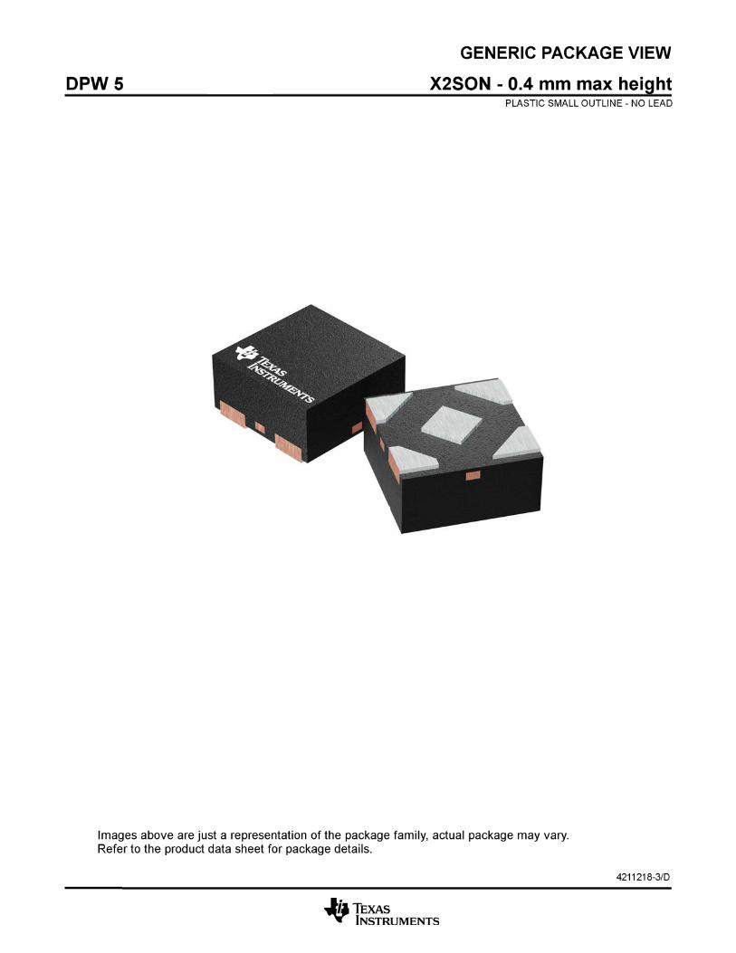
SN74LVC1G08 Single 2-Input Positive-AND Gate1 Features 3 Description
This single 2-input positive-AND gate is designed for1• Available in the Ultra Small 0.64-mm2
1.65-V to 5.5-V VCC operation.Package (DPW) With 0.5-mm PitchThe SN74LVC1G08 device performs the Boolean• Supports 5-V VCC Operationfunction or in positive logic.• Inputs Accept Voltages to 5.5 VThe CMOS device has high output drive while• Provides Down Translation to VCCmaintaining low static power dissipation over a broad• Max tpd of 3.6 ns at 3.3 VVCC operating range.
• Low Power Consumption, 10-μA Max ICCThe SN74LVC1G08 is available in a variety of• ±24-mA Output Drive at 3.3 V packages, including the ultra-small DPW package
• Ioff Supports Live Insertion, Partial-Power-Down with a body size of 0.8 mm × 0.8 mm.Mode, and Back Drive Protection
white space• Latch-Up Performance Exceeds 100 mAwhite spacePer JESD 78, Class II
• ESD Protection Exceeds JESD 22 Device Information(1)– 2000-V Human-Body Model (A114-A) DEVICE NAME PACKAGE BODY SIZE– 200-V Machine Model (A115-A) SOT-23 (5) 2.9mm × 1.6mm– 1000-V Charged-Device Model (C101) SC70 (5) 2.0mm × 1.25mm
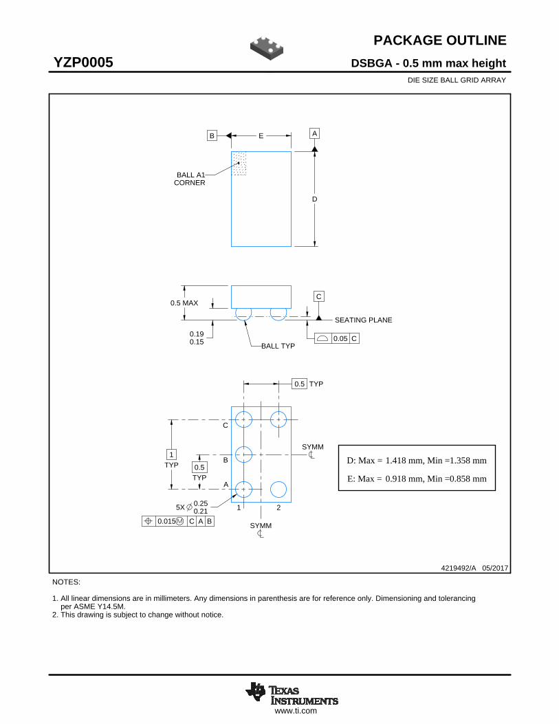
SN74LVC1G08 X2SON (4) 0.8mm × 0.8mm2 ApplicationsSON (6) 1.45mm × 1.0mm
• ATCA Solutions SON (6) 1.0mm × 1.0mm• Active Noise Cancellation (ANC) (1) For all available packages, see the orderable addendum at
the end of the datasheet.• Barcode Scanner• Blood Pressure Monitor• CPAP Machine• Cable Solutions• DLP 3D Machine Vision, Hyperspectral Imaging,
Optical Networking, and Spectroscopy• E-Book• Embedded PC• Field Transmitter: Temperature or Pressure
Sensor• Fingerprint Biometrics• HVAC: Heating, Ventilating, and Air Conditioning• Network-Attached Storage (NAS)• Server Motherboard and PSU• Software Defined Radio (SDR)• TV: High-Definition (HDTV), LCD, and Digital• Video Communications System• Wireless Data Access Card, Headset, Keyboard,
Mouse, and LAN Card• X-ray: Baggage Scanner, Medical, and Dental
1
An IMPORTANT NOTICE at the end of this data sheet addresses availability, warranty, changes, use in safety-critical applications,intellectual property matters and other important disclaimers. PRODUCTION DATA.

SN74LVC1G08SCES217Y –APRIL 1999–REVISED APRIL 2014 www.ti.com
Table of Contents1 Features .................................................................. 1 8 Detailed Description ............................................ 10
8.1 Overview ................................................................. 102 Applications ........................................................... 18.2 Functional Block Diagram ....................................... 103 Description ............................................................. 18.3 Feature Description................................................. 104 Revision History..................................................... 28.4 Device Functional Modes........................................ 105 Pin Configuration and Functions ......................... 3
9 Application and Implementation ........................ 116 Specifications......................................................... 49.1 Application Information............................................ 116.1 Absolute Maximum Ratings ..................................... 49.2 Typical Application ................................................. 116.2 Handling Ratings....................................................... 4
10 Power Supply Recommendations ..................... 126.3 Recommended Operating Conditions ...................... 511 Layout................................................................... 126.4 Thermal Information .................................................. 5
11.1 Layout Guidelines ................................................. 126.5 Electrical Characteristics........................................... 611.2 Layout Example .................................................... 126.6 Switching Characteristics, CL = 15 pF ...................... 6
12 Device and Documentation Support ................. 136.7 Switching Characteristics, 1.8 V and 2.5 V .............. 612.1 Trademarks ........................................................... 136.8 Switching Characteristics, 3.3 V and 5 V ................. 712.2 Electrostatic Discharge Caution............................ 136.9 Operating Characteristics.......................................... 712.3 Glossary ................................................................ 136.10 Typical Characteristics ............................................ 7
13 Mechanical, Packaging, and Orderable7 Parameter Measurement Information .................. 8Information ........................................................... 13
4 Revision History
Changes from Revision X (March 2014) to Revision Y Page
• Updated Handling Ratings table. ........................................................................................................................................... 4• Added Thermal Information table. ......................................................................................................................................... 5• Added Typical Characteristics. .............................................................................................................................................. 7• Added Detailed Description section. .................................................................................................................................... 10• Added Application and Implementation section. ................................................................................................................. 11• Added Power Supply Recommendations section. .............................................................................................................. 12• Added Layout section. ......................................................................................................................................................... 12
Changes from Revision W (July 2013) to Revision X Page
• Added Applications. ................................................................................................................................................................ 1• Added Device Information table. ............................................................................................................................................ 1• Moved Tstg to Handling Ratings table. .................................................................................................................................... 4
Changes from Revision V (November 2012) to Revision W Page
• Added parameter values for –40 to 125°C temperature ratings............................................................................................. 6
2 Submit Documentation Feedback Copyright © 1999–2014, Texas Instruments Incorporated
Product Folder Links: SN74LVC1G08

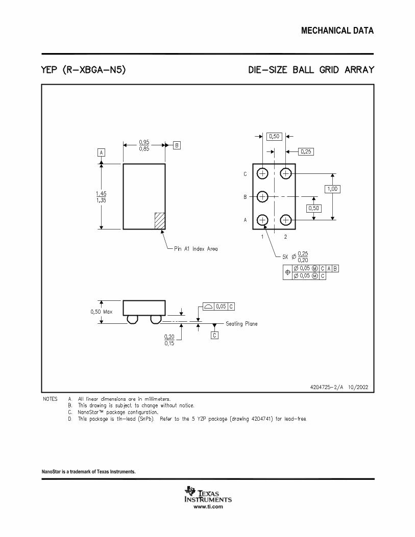
DBV PACKAGE(TOP VIEW)
2
5
3 4 Y
1
B
GND
A VCC
DCK PACKAGE(TOP VIEW)
3 4GND
2B
Y
1A 5 VCC
DRL PACKAGE(TOP VIEW)
2B
1A
3 4GND Y
5 VCC
1 5
2
3
AGND
Y
VCC
DPW PACKAGE
(TOP VIEW)
B
4
GND
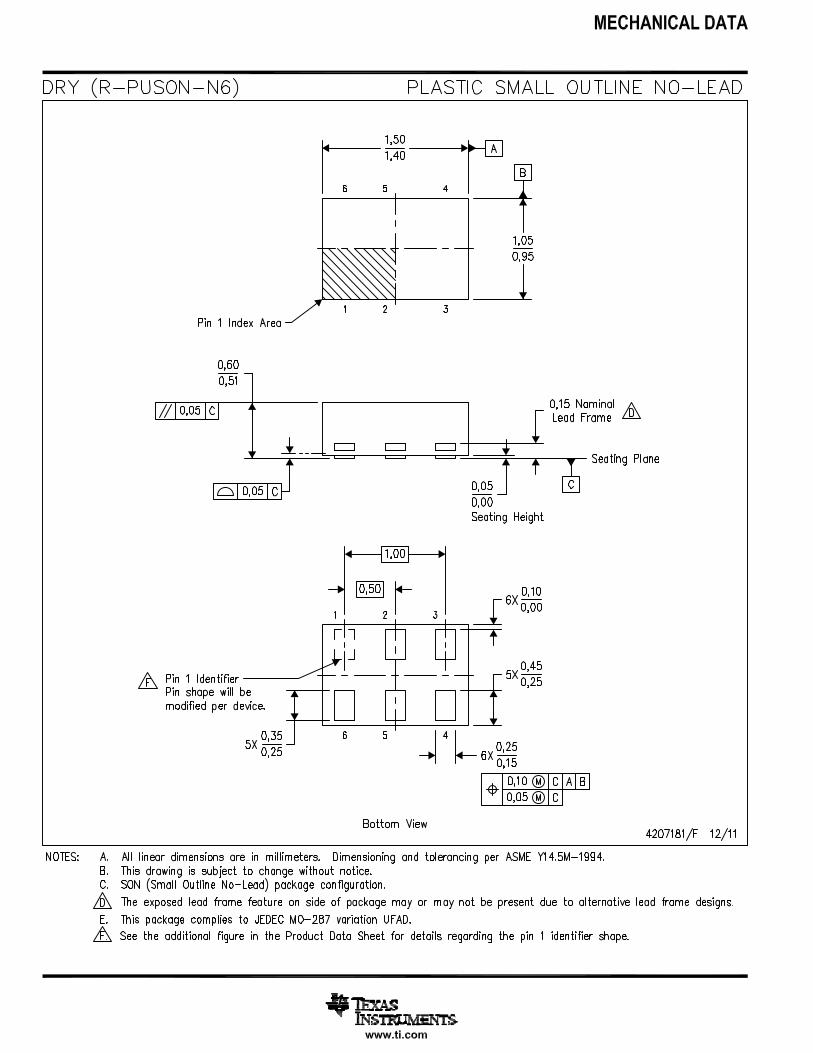
DRY PACKAGE(TOP VIEW)
B NC
A 6
5
4
2
3 Y
VCC
1
YZP PACKAGE(BOTTOM VIEW)
2B
1A
GND 43 Y
5 VCC
6
5
4
2
3
1
DSF PACKAGE(TOP VIEW)
B
A
GND
NC
Y
VCC
SN74LVC1G08www.ti.com SCES217Y –APRIL 1999–REVISED APRIL 2014
5 Pin Configuration and Functions
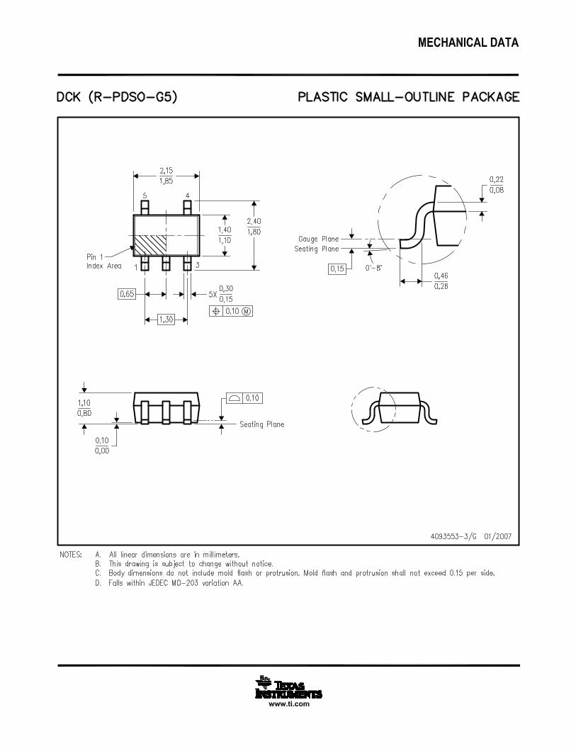
NC – No internal connectionSee mechanical drawings for dimensions.
Pin FunctionsPIN
DESCRIPTIONDBV, DCK,NAME DRY, DSF DPWDRL, YZP
A 1 1 2 Input
B 2 2 1 Input
GND 3 3 3 Ground
Y 4 4 4 Output
VCC 5 6 5 Power pin
NC 5 Not connected
Copyright © 1999–2014, Texas Instruments Incorporated Submit Documentation Feedback 3
Product Folder Links: SN74LVC1G08
SN74LVC1G08SCES217Y –APRIL 1999–REVISED APRIL 2014 www.ti.com
6 Specifications
6.1 Absolute Maximum Ratings (1)
over operating free-air temperature range (unless otherwise noted)MIN MAX UNIT
VCC Supply voltage range –0.5 6.5 VVI Input voltage range (2) –0.5 6.5 VVO Voltage range applied to any output in the high-impedance or power-off state (2) –0.5 6.5 VVO Voltage range applied to any output in the high or low state (2) (3) –0.5 VCC + 0.5 VIIK Input clamp current VI < 0 –50 mAIOK Output clamp current VO < 0 –50 mAIO Continuous output current ±50 mA
Continuous current through VCC or GND ±100 mA
(1) Stresses beyond those listed under Absolute Maximum Ratings may cause permanent damage to the device. These are stress ratingsonly, and functional operation of the device at these or any other conditions beyond those indicated under Recommended OperatingConditions is not implied. Exposure to absolute-maximum-rated conditions for extended periods may affect device reliability.
(2) The input and output negative-voltage ratings may be exceeded if the input and output current ratings are observed.(3) The value of VCC is provided in the Recommended Operating Conditions table.
6.2 Handling RatingsMIN MAX UNIT
Tstg Storage temperature range –65 150 °CHuman body model (HBM), per ANSI/ESDA/JEDEC JS-001, all 0 2000pins (1)
V(ESD) Electrostatic discharge VCharged device model (CDM), per JEDEC specification 0 1000JESD22-C101, all pins (2)
(1) JEDEC document JEP155 states that 500-V HBM allows safe manufacturing with a standard ESD control process.(2) JEDEC document JEP157 states that 250-V CDM allows safe manufacturing with a standard ESD control process.
4 Submit Documentation Feedback Copyright © 1999–2014, Texas Instruments Incorporated
Product Folder Links: SN74LVC1G08
SN74LVC1G08www.ti.com SCES217Y –APRIL 1999–REVISED APRIL 2014
6.3 Recommended Operating Conditions (1)
MIN MAX UNITOperating 1.65 5.5
VCC Supply voltage VData retention only 1.5VCC = 1.65 V to 1.95 V 0.65 × VCC
VCC = 2.3 V to 2.7 V 1.7VIH High-level input voltage V
VCC = 3 V to 3.6 V 2VCC = 4.5 V to 5.5 V 0.7 × VCC
VCC = 1.65 V to 1.95 V 0.35 × VCC
VCC = 2.3 V to 2.7 V 0.7VIL Low-level input voltage V
VCC = 3 V to 3.6 V 0.8VCC = 4.5 V to 5.5 V 0.3 × VCC
VI Input voltage 0 5.5 VVO Output voltage 0 VCC V
VCC = 1.65 V –4VCC = 2.3 V –8
IOH High-level output current –16 mAVCC = 3 V
–24VCC = 4.5 V –32VCC = 1.65 V 4VCC = 2.3 V 8
IOL Low-level output current 16 mAVCC = 3 V
24VCC = 4.5 V 32VCC = 1.8 V ± 0.15 V, 2.5 V ± 0.2 V 20
Δt/Δv Input transition rise or fall rate VCC = 3.3 V ± 0.3 V 10 ns/VVCC = 5 V ± 0.5 V 5
TA Operating free-air temperature –40 125 °C
(1) All unused inputs of the device must be held at VCC or GND to ensure proper device operation. Refer to the TI application report,Implications of Slow or Floating CMOS Inputs, literature number SCBA004.
6.4 Thermal InformationSN74LVC1G08
THERMAL METRIC (1) DBV DCK DRL DRY YZP DPW UNIT
5 PINS 5 PINS 5 PINS 6 PINS 5 PINS 4 PINS
RθJA Junction-to-ambient thermal resistance 207.6 283.1 242.9 438.8 130 340
RθJCtop Junction-to-case (top) thermal resistance 145.2 92.3 77.5 276.8 54 215
RθJB Junction-to-board thermal resistance 53.5 60.9 77.5 271.7 51 294°C/W
ψJT Junction-to-top characterization parameter 37.5 1.7 9.6 83.8 1 41
ψJB Junction-to-board characterization parameter 53.1 60.1 77.3 271.4 50 294
RθJCbot Junction-to-case (bottom) thermal resistance – – – – – 250
(1) For more information about traditional and new thermal metrics, see the IC Package Thermal Metrics application report, SPRA953.
Copyright © 1999–2014, Texas Instruments Incorporated Submit Documentation Feedback 5
Product Folder Links: SN74LVC1G08
SN74LVC1G08SCES217Y –APRIL 1999–REVISED APRIL 2014 www.ti.com
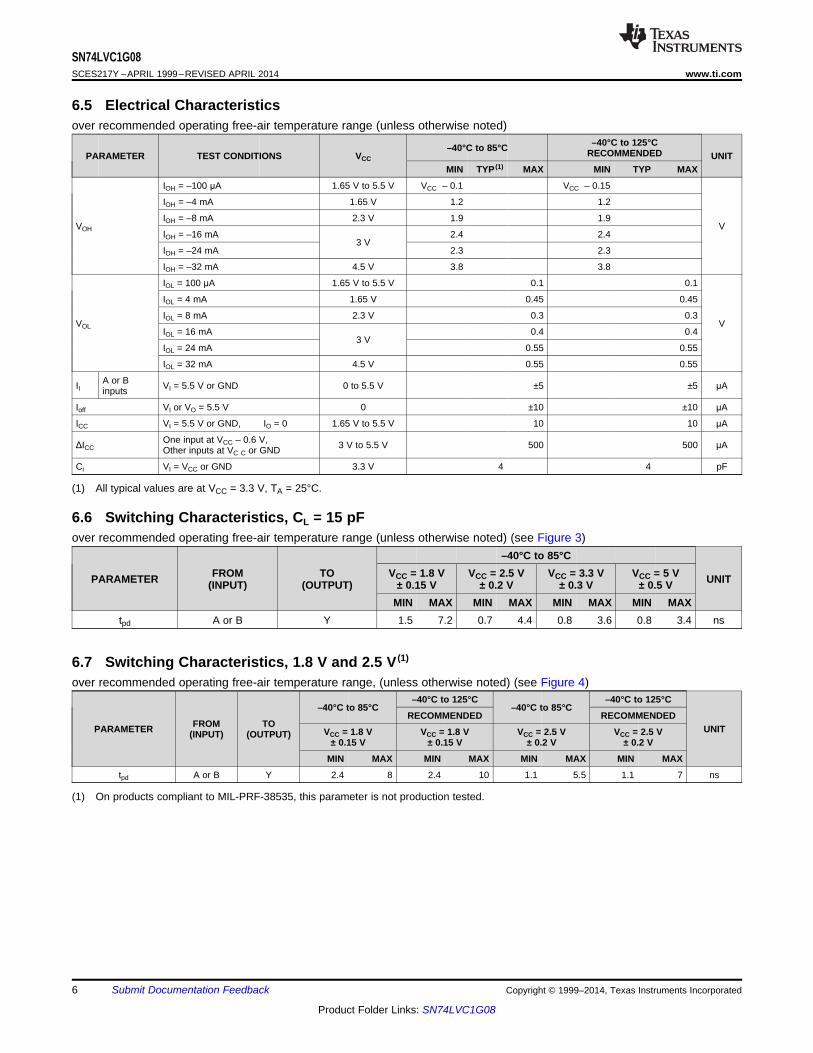
6.5 Electrical Characteristicsover recommended operating free-air temperature range (unless otherwise noted)
–40°C to 125°C–40°C to 85°C RECOMMENDEDPARAMETER TEST CONDITIONS VCC UNITMIN TYP (1) MAX MIN TYP MAX
IOH = –100 μA 1.65 V to 5.5 V VCC – 0.1 VCC – 0.15
IOH = –4 mA 1.65 V 1.2 1.2
IOH = –8 mA 2.3 V 1.9 1.9VOH V
IOH = –16 mA 2.4 2.43 V
IOH = –24 mA 2.3 2.3
IOH = –32 mA 4.5 V 3.8 3.8
IOL = 100 μA 1.65 V to 5.5 V 0.1 0.1
IOL = 4 mA 1.65 V 0.45 0.45
IOL = 8 mA 2.3 V 0.3 0.3VOL V
IOL = 16 mA 0.4 0.43 V
IOL = 24 mA 0.55 0.55
IOL = 32 mA 4.5 V 0.55 0.55
A or BII VI = 5.5 V or GND 0 to 5.5 V ±5 ±5 μAinputs
Ioff VI or VO = 5.5 V 0 ±10 ±10 μA
ICC VI = 5.5 V or GND, IO = 0 1.65 V to 5.5 V 10 10 μA
One input at VCC – 0.6 V,ΔICC 3 V to 5.5 V 500 500 μAOther inputs at VC C or GND
Ci VI = VCC or GND 3.3 V 4 4 pF
(1) All typical values are at VCC = 3.3 V, TA = 25°C.
6.6 Switching Characteristics, CL = 15 pFover recommended operating free-air temperature range (unless otherwise noted) (see Figure 3)
–40°C to 85°CFROM TO VCC = 1.8 V VCC = 2.5 V VCC = 3.3 V VCC = 5 VPARAMETER UNIT(INPUT) (OUTPUT) ± 0.15 V ± 0.2 V ± 0.3 V ± 0.5 V
MIN MAX MIN MAX MIN MAX MIN MAXtpd A or B Y 1.5 7.2 0.7 4.4 0.8 3.6 0.8 3.4 ns
6.7 Switching Characteristics, 1.8 V and 2.5 V (1)
over recommended operating free-air temperature range, (unless otherwise noted) (see Figure 4)–40°C to 125°C –40°C to 125°C
–40°C to 85°C –40°C to 85°CRECOMMENDED RECOMMENDED
FROM TOPARAMETER UNITVCC = 1.8 V VCC = 1.8 V VCC = 2.5 V VCC = 2.5 V(INPUT) (OUTPUT)± 0.15 V ± 0.15 V ± 0.2 V ± 0.2 V
MIN MAX MIN MAX MIN MAX MIN MAX
tpd A or B Y 2.4 8 2.4 10 1.1 5.5 1.1 7 ns
(1) On products compliant to MIL-PRF-38535, this parameter is not production tested.
6 Submit Documentation Feedback Copyright © 1999–2014, Texas Instruments Incorporated
Product Folder Links: SN74LVC1G08

Temperature - °C
TPD
- ns
-100 -50 0 50 100 1500
1
2
3
4
5
6
D001
TPD
Vcc - V
TPD
- ns
0 1 2 3 4 5 60
1
2
3
4
5
6
7
8
D002
TPD
SN74LVC1G08www.ti.com SCES217Y –APRIL 1999–REVISED APRIL 2014
6.8 Switching Characteristics, 3.3 V and 5 V (1)
over recommended operating free-air temperature range, CL = 30 pF or 50 pF (unless otherwise noted) (see Figure 4)–40°C to 125°C –40°C to 125°C
–40°C to 85°C –40°C to 85°CRECOMMENDED RECOMMENDED
FROM TOPARAMETER UNITVCC = 3.3 V VCC = 3.3 V VCC = 5 V VCC = 5 V(INPUT) (OUTPUT)± 0.3 V ± 0.3 V ± 0.5 V ± 0.5 V
MIN MAX MIN MAX MIN MAX MIN MAX
tpd A or B Y 1 4.5 1 6 1 4 1 5 ns
(1) On products compliant to MIL-PRF-38535, this parameter is not production tested.
6.9 Operating CharacteristicsTA = 25°C
VCC = 1.8 V VCC = 2.5 V VCC = 3.3 V VCC = 5 VTESTPARAMETER UNITCONDITIONS TYP TYP TYP TYPCpd Power dissipation capacitance f = 10 MHz 21 24 26 31 pF
6.10 Typical Characteristics
Figure 1. TPD Across Temperature at 3.3V Vcc Figure 2. TPD Across Vcc at 25°C
Copyright © 1999–2014, Texas Instruments Incorporated Submit Documentation Feedback 7
Product Folder Links: SN74LVC1G08
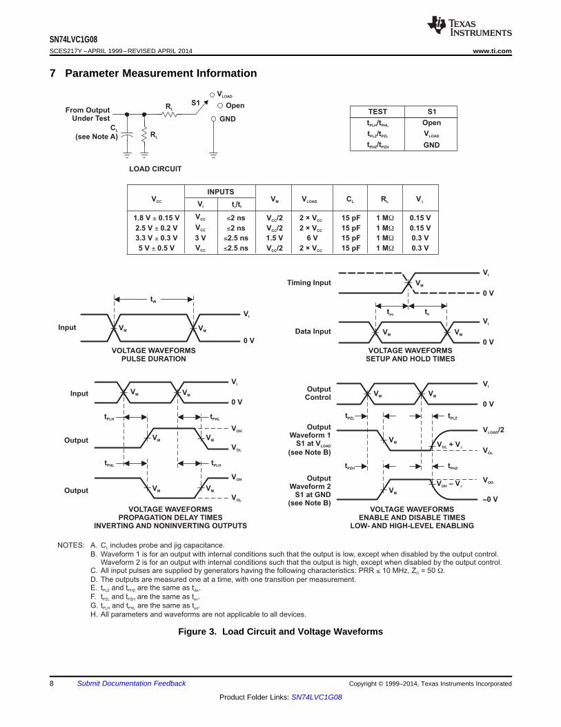
thtsu
From OutputUnder Test
C
(see Note A)L
LOAD CIRCUIT
S1
VLOAD
Open
GND
RL
Data Input
Timing Input
0 V
0 V0 V
tW
Input
0 VInput
OutputWaveform 1
S1 at V
(see Note B)LOAD
OutputWaveform 2
S1 at GND(see Note B)
VOL
VOH
0 V
»0 V
Output
Output
t /tPLH PHL Open
TEST S1
OutputControl
VM
VM VM
VM
VM
1.8 V 0.15 V±
2.5 V 0.2 V±
3.3 V 0.3 V±
5 V 0.5 V±
1 MW
1 MW
1 MW
1 MW
VCC RL
2 × VCC
2 × VCC
6 V
2 × VCC
VLOAD CL
15 pF
15 pF
15 pF
15 pF
0.15 V
0.15 V
0.3 V
0.3 V
VD
3 V
VI
VCC/2
VCC/2
1.5 V
VCC/2
VM
£2 ns
£2 ns
£2.5 ns
£2.5 ns
INPUTS
RL
t /tr f
VCC
VCC
VCC
VLOADt /tPLZ PZL
GNDt /tPHZ PZH
VOLTAGE WAVEFORMSENABLE AND DISABLE TIMES
LOW- AND HIGH-LEVEL ENABLING
VOLTAGE WAVEFORMSPROPAGATION DELAY TIMES
INVERTING AND NONINVERTING OUTPUTS
NOTES: A. C includes probe and jig capacitance.
B. Waveform 1 is for an output with internal conditions such that the output is low, except when disabled by the output control.Waveform 2 is for an output with internal conditions such that the output is high, except when disabled by the output control.
C. All input pulses are supplied by generators having the following characteristics: PRR 10 MHz, Z = 50 .
D. The outputs are measured one at a time, with one transition per measurement.E. t and t are the same as t .
F. t and t are the same as t .
G. t and t are the same as t .
H. All parameters and waveforms are not applicable to all devices.
L
O
PLZ PHZ dis
PZL PZH en
PLH PHL pd
£ W
VOLTAGE WAVEFORMSPULSE DURATION
VOLTAGE WAVEFORMSSETUP AND HOLD TIMES
VI
VI
VI
VM
VM
V /2LOAD
tPZL tPLZ
tPHZtPZH
V – VOH D
V + VOL D
VM
VM VM
VM
VOL
VOH
VI
VI
VOH
VOL
VM
VM
VM
VM
tPLH tPHL
tPLHtPHL
SN74LVC1G08SCES217Y –APRIL 1999–REVISED APRIL 2014 www.ti.com
7 Parameter Measurement Information
Figure 3. Load Circuit and Voltage Waveforms
8 Submit Documentation Feedback Copyright © 1999–2014, Texas Instruments Incorporated
Product Folder Links: SN74LVC1G08

thtsu
From OutputUnder Test
C
(see Note A)L
LOAD CIRCUIT
S1
VLOAD
Open
GND
RL
Data Input
Timing Input
0 V
0 V0 V
tW
Input
0 VInput
OutputWaveform 1
S1 at V
(see Note B)LOAD
OutputWaveform 2
S1 at GND(see Note B)
VOL
VOH
0 V
»0 V
Output
Output
TEST S1
t /tPLH PHL Open
OutputControl
VM
VM VM
VM
VM
1.8 V 0.15 V±
2.5 V 0.2 V±
3.3 V 0.3 V±
5 V 0.5 V±
1 kW
500 W
500 W
500 W
VCC RL
2 × VCC
2 × VCC
6 V
2 × VCC
VLOAD CL
30 pF
30 pF
50 pF
50 pF
0.15 V
0.15 V
0.3 V
0.3 V
VD
3 V
VI
VCC/2
VCC/2
1.5 V
VCC/2
VM
£2 ns
£2 ns
£2.5 ns
£2.5 ns
INPUTS
RL
t /tr f
VCC
VCC
VCC
VLOADt /tPLZ PZL
GNDt /tPHZ PZH
VOLTAGE WAVEFORMSENABLE AND DISABLE TIMES
LOW- AND HIGH-LEVEL ENABLING
VOLTAGE WAVEFORMSPROPAGATION DELAY TIMES
INVERTING AND NONINVERTING OUTPUTS
NOTES: A. C includes probe and jig capacitance.
B. Waveform 1 is for an output with internal conditions such that the output is low, except when disabled by the output control.Waveform 2 is for an output with internal conditions such that the output is high, except when disabled by the output control.
C. All input pulses are supplied by generators having the following characteristics: PRR 10 MHz, Z = 50 .
D. The outputs are measured one at a time, with one transition per measurement.E. t and t are the same as t .
F. t and t are the same as t .
G. t and t are the same as t .
H. All parameters and waveforms are not applicable to all devices.
L
O
PLZ PHZ dis
PZL PZH en
PLH PHL pd
£ W
VOLTAGE WAVEFORMSPULSE DURATION
VOLTAGE WAVEFORMSSETUP AND HOLD TIMES
VI
VI
VI
VM
VM
V /2LOAD
tPZL tPLZ
tPHZtPZH
V – VOH D
V + VOL D
VM
VM VM
VM
VOL
VOH
VI
VI
VOH
VOL
VM
VM
VM
VM
tPLH tPHL
tPLHtPHL
SN74LVC1G08www.ti.com SCES217Y –APRIL 1999–REVISED APRIL 2014
Parameter Measurement Information (continued)
Figure 4. Load Circuit and Voltage Waveforms
Copyright © 1999–2014, Texas Instruments Incorporated Submit Documentation Feedback 9
Product Folder Links: SN74LVC1G08
Y = A • B or Y = +A B
SN74LVC1G08SCES217Y –APRIL 1999–REVISED APRIL 2014 www.ti.com
8 Detailed Description
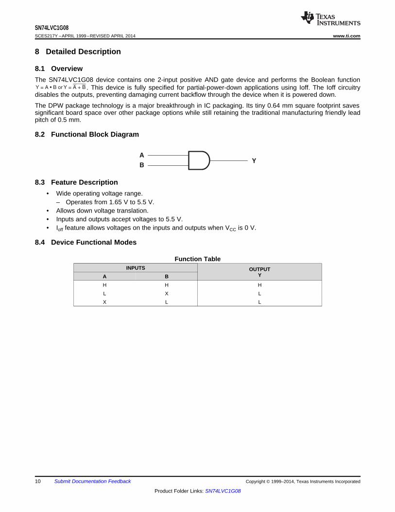
8.1 OverviewThe SN74LVC1G08 device contains one 2-input positive AND gate device and performs the Boolean function
. This device is fully specified for partial-power-down applications using Ioff. The Ioff circuitrydisables the outputs, preventing damaging current backflow through the device when it is powered down.
The DPW package technology is a major breakthrough in IC packaging. Its tiny 0.64 mm square footprint savessignificant board space over other package options while still retaining the traditional manufacturing friendly leadpitch of 0.5 mm.
8.2 Functional Block Diagram
8.3 Feature Description• Wide operating voltage range.
– Operates from 1.65 V to 5.5 V.• Allows down voltage translation.• Inputs and outputs accept voltages to 5.5 V.• Ioff feature allows voltages on the inputs and outputs when VCC is 0 V.
8.4 Device Functional Modes
Function TableINPUTS OUTPUT
YA BH H HL X LX L L
10 Submit Documentation Feedback Copyright © 1999–2014, Texas Instruments Incorporated
Product Folder Links: SN74LVC1G08
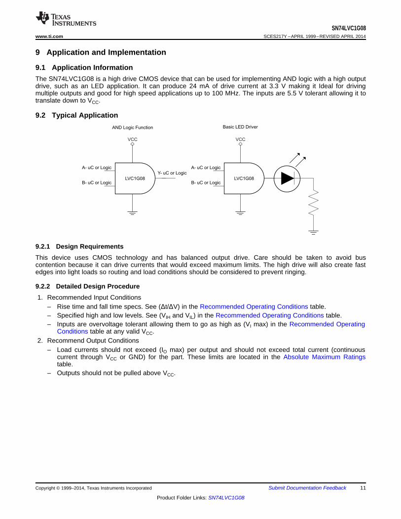
LVC1G08
A- uC or Logic
B- uC or Logic
Basic LED Driver
A- uC or Logic
B- uC or Logic
Y- uC or Logic
AND Logic Function
LVC1G08
VCC VCC
SN74LVC1G08www.ti.com SCES217Y –APRIL 1999–REVISED APRIL 2014
9 Application and Implementation
9.1 Application InformationThe SN74LVC1G08 is a high drive CMOS device that can be used for implementing AND logic with a high outputdrive, such as an LED application. It can produce 24 mA of drive current at 3.3 V making it Ideal for drivingmultiple outputs and good for high speed applications up to 100 MHz. The inputs are 5.5 V tolerant allowing it totranslate down to VCC.
9.2 Typical Application
9.2.1 Design RequirementsThis device uses CMOS technology and has balanced output drive. Care should be taken to avoid buscontention because it can drive currents that would exceed maximum limits. The high drive will also create fastedges into light loads so routing and load conditions should be considered to prevent ringing.
9.2.2 Detailed Design Procedure1. Recommended Input Conditions
– Rise time and fall time specs. See (Δt/ΔV) in the Recommended Operating Conditions table.– Specified high and low levels. See (VIH and VIL) in the Recommended Operating Conditions table.– Inputs are overvoltage tolerant allowing them to go as high as (VI max) in the Recommended Operating
Conditions table at any valid VCC.2. Recommend Output Conditions
– Load currents should not exceed (IO max) per output and should not exceed total current (continuouscurrent through VCC or GND) for the part. These limits are located in the Absolute Maximum Ratingstable.
– Outputs should not be pulled above VCC.
Copyright © 1999–2014, Texas Instruments Incorporated Submit Documentation Feedback 11
Product Folder Links: SN74LVC1G08
VCC
Unused Input
Input
Output Output
Input
Unused Input
Frequency - MHz
Icc
- mA
-20 0 20 40 60 80-2
0
2
4
6
8
10
D003
Icc 1.8VIcc 2.5VIcc 3.3VIcc 5V
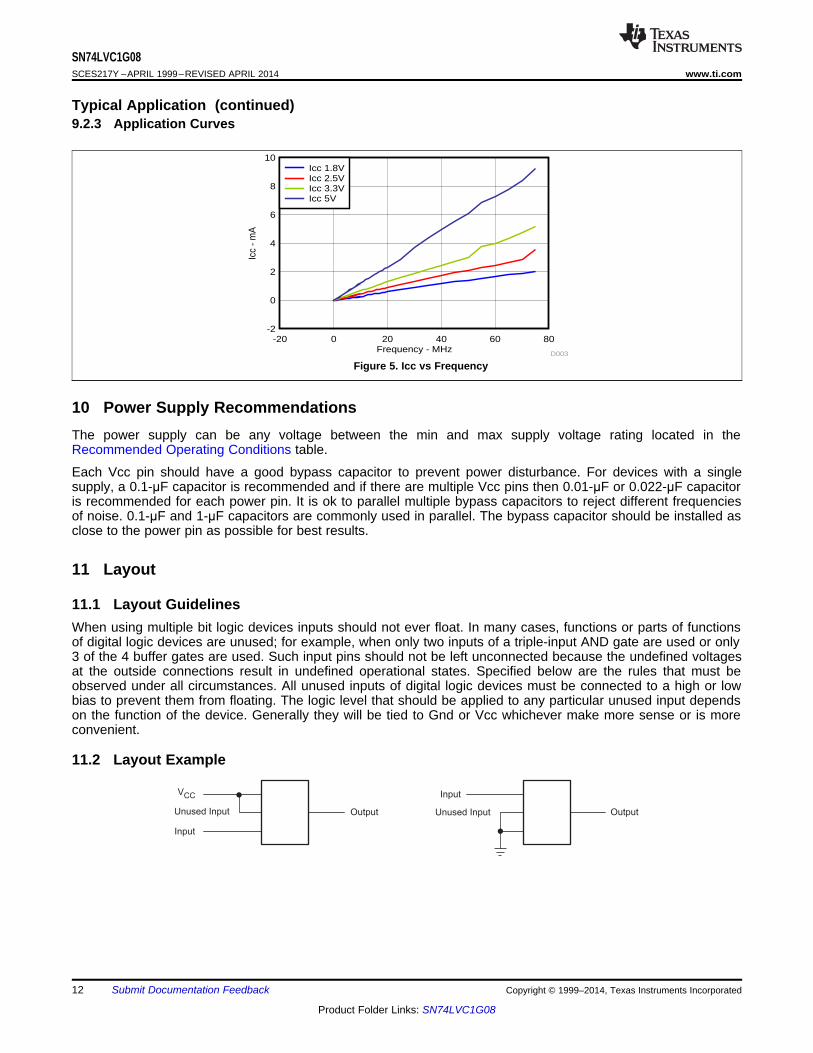
SN74LVC1G08SCES217Y –APRIL 1999–REVISED APRIL 2014 www.ti.com
Typical Application (continued)9.2.3 Application Curves
Figure 5. Icc vs Frequency
10 Power Supply RecommendationsThe power supply can be any voltage between the min and max supply voltage rating located in theRecommended Operating Conditions table.
Each Vcc pin should have a good bypass capacitor to prevent power disturbance. For devices with a singlesupply, a 0.1-μF capacitor is recommended and if there are multiple Vcc pins then 0.01-μF or 0.022-μF capacitoris recommended for each power pin. It is ok to parallel multiple bypass capacitors to reject different frequenciesof noise. 0.1-μF and 1-μF capacitors are commonly used in parallel. The bypass capacitor should be installed asclose to the power pin as possible for best results.
11 Layout
11.1 Layout GuidelinesWhen using multiple bit logic devices inputs should not ever float. In many cases, functions or parts of functionsof digital logic devices are unused; for example, when only two inputs of a triple-input AND gate are used or only3 of the 4 buffer gates are used. Such input pins should not be left unconnected because the undefined voltagesat the outside connections result in undefined operational states. Specified below are the rules that must beobserved under all circumstances. All unused inputs of digital logic devices must be connected to a high or lowbias to prevent them from floating. The logic level that should be applied to any particular unused input dependson the function of the device. Generally they will be tied to Gnd or Vcc whichever make more sense or is moreconvenient.
11.2 Layout Example
12 Submit Documentation Feedback Copyright © 1999–2014, Texas Instruments Incorporated
Product Folder Links: SN74LVC1G08
SN74LVC1G08www.ti.com SCES217Y –APRIL 1999–REVISED APRIL 2014
12 Device and Documentation Support
12.1 TrademarksAll trademarks are the property of their respective owners.
12.2 Electrostatic Discharge CautionThese devices have limited built-in ESD protection. The leads should be shorted together or the device placed in conductive foamduring storage or handling to prevent electrostatic damage to the MOS gates.
12.3 GlossarySLYZ022 — TI Glossary.
This glossary lists and explains terms, acronyms and definitions.
13 Mechanical, Packaging, and Orderable InformationThe following pages include mechanical packaging and orderable information. This information is the mostcurrent data available for the designated devices. This data is subject to change without notice and revision ofthis document. For browser-based versions of this data sheet, refer to the left-hand navigation.
Copyright © 1999–2014, Texas Instruments Incorporated Submit Documentation Feedback 13
Product Folder Links: SN74LVC1G08
PACKAGE OPTION ADDENDUM
www.ti.com 28-Nov-2017
Addendum-Page 1
PACKAGING INFORMATION
Orderable Device Status(1)
Package Type PackageDrawing
Pins PackageQty
Eco Plan(2)
Lead/Ball Finish(6)
MSL Peak Temp(3)
Op Temp (°C) Device Marking(4/5)
Samples
SN74LVC1G08DBVR ACTIVE SOT-23 DBV 5 3000 Green (RoHS& no Sb/Br)
CU NIPDAU Level-1-260C-UNLIM -40 to 125 (C085, C08F, C08K, C08R, C08T)(C08P, C08S)
SN74LVC1G08DBVRE4 ACTIVE SOT-23 DBV 5 3000 Green (RoHS& no Sb/Br)
CU NIPDAU Level-1-260C-UNLIM -40 to 125 (C085, C08F, C08K, C08R, C08T)(C08P, C08S)
SN74LVC1G08DBVRG4 ACTIVE SOT-23 DBV 5 3000 Green (RoHS& no Sb/Br)
CU NIPDAU Level-1-260C-UNLIM -40 to 125 (C085, C08F, C08K, C08R, C08T)(C08P, C08S)
SN74LVC1G08DBVT ACTIVE SOT-23 DBV 5 250 Green (RoHS& no Sb/Br)
CU NIPDAU Level-1-260C-UNLIM -40 to 125 (C085, C08F, C08K, C08R)(C08H, C08P, C08S)
SN74LVC1G08DBVTE4 ACTIVE SOT-23 DBV 5 250 Green (RoHS& no Sb/Br)
CU NIPDAU Level-1-260C-UNLIM -40 to 125 (C085, C08F, C08K, C08R)(C08H, C08P, C08S)
SN74LVC1G08DBVTG4 ACTIVE SOT-23 DBV 5 250 Green (RoHS& no Sb/Br)
CU NIPDAU Level-1-260C-UNLIM -40 to 125 (C085, C08F, C08K, C08R)(C08H, C08P, C08S)
SN74LVC1G08DCKR ACTIVE SC70 DCK 5 3000 Green (RoHS& no Sb/Br)
CU NIPDAU Level-1-260C-UNLIM -40 to 125 (CE5, CEF, CEK, CE R, CET)(CEH, CEP, CES)
SN74LVC1G08DCKRE4 ACTIVE SC70 DCK 5 3000 Green (RoHS& no Sb/Br)
CU NIPDAU Level-1-260C-UNLIM -40 to 125 (CE5, CEF, CEK, CE R, CET)(CEH, CEP, CES)
SN74LVC1G08DCKRG4 ACTIVE SC70 DCK 5 3000 Green (RoHS& no Sb/Br)
CU NIPDAU Level-1-260C-UNLIM -40 to 125 (CE5, CEF, CEK, CE R, CET)(CEH, CEP, CES)
SN74LVC1G08DCKT ACTIVE SC70 DCK 5 250 Green (RoHS& no Sb/Br)
CU NIPDAU Level-1-260C-UNLIM -40 to 125 (CE5, CEF, CEK, CE R, CET)(CEH, CEP, CES)
SN74LVC1G08DCKTE4 ACTIVE SC70 DCK 5 250 Green (RoHS& no Sb/Br)
CU NIPDAU Level-1-260C-UNLIM -40 to 125 (CE5, CEF, CEK, CE R, CET)(CEH, CEP, CES)
PACKAGE OPTION ADDENDUM
www.ti.com 28-Nov-2017
Addendum-Page 2
Orderable Device Status(1)
Package Type PackageDrawing
Pins PackageQty
Eco Plan(2)
Lead/Ball Finish(6)
MSL Peak Temp(3)
Op Temp (°C) Device Marking(4/5)
Samples
SN74LVC1G08DCKTG4 ACTIVE SC70 DCK 5 250 Green (RoHS& no Sb/Br)
CU NIPDAU Level-1-260C-UNLIM -40 to 125 (CE5, CEF, CEK, CE R, CET)(CEH, CEP, CES)
SN74LVC1G08DPWR ACTIVE X2SON DPW 5 3000 Green (RoHS& no Sb/Br)
CU NIPDAU Level-1-260C-UNLIM -40 to 125 M4
SN74LVC1G08DRLR ACTIVE SOT-5X3 DRL 5 4000 Green (RoHS& no Sb/Br)
CU NIPDAU Level-1-260C-UNLIM -40 to 125 (CE7, CER)
SN74LVC1G08DRLRG4 ACTIVE SOT-5X3 DRL 5 4000 Green (RoHS& no Sb/Br)
CU NIPDAU Level-1-260C-UNLIM -40 to 125 (CE7, CER)
SN74LVC1G08DRY2 ACTIVE SON DRY 6 5000 Green (RoHS& no Sb/Br)
CU NIPDAU Level-1-260C-UNLIM -40 to 125 CE
SN74LVC1G08DRYR ACTIVE SON DRY 6 5000 Green (RoHS& no Sb/Br)
CU NIPDAU Level-1-260C-UNLIM -40 to 125 CE
SN74LVC1G08DSF2 ACTIVE SON DSF 6 5000 Green (RoHS& no Sb/Br)
CU NIPDAU |CU NIPDAUAG
Level-1-260C-UNLIM -40 to 125 CE
SN74LVC1G08DSFR ACTIVE SON DSF 6 5000 Green (RoHS& no Sb/Br)
CU NIPDAU |CU NIPDAUAG
Level-1-260C-UNLIM -40 to 125 CE
SN74LVC1G08YZPR ACTIVE DSBGA YZP 5 3000 Green (RoHS& no Sb/Br)
SNAGCU Level-1-260C-UNLIM -40 to 85 (CE, CE7)
(1) The marketing status values are defined as follows:ACTIVE: Product device recommended for new designs.LIFEBUY: TI has announced that the device will be discontinued, and a lifetime-buy period is in effect.NRND: Not recommended for new designs. Device is in production to support existing customers, but TI does not recommend using this part in a new design.PREVIEW: Device has been announced but is not in production. Samples may or may not be available.OBSOLETE: TI has discontinued the production of the device.
(2) RoHS: TI defines "RoHS" to mean semiconductor products that are compliant with the current EU RoHS requirements for all 10 RoHS substances, including the requirement that RoHS substancedo not exceed 0.1% by weight in homogeneous materials. Where designed to be soldered at high temperatures, "RoHS" products are suitable for use in specified lead-free processes. TI mayreference these types of products as "Pb-Free".RoHS Exempt: TI defines "RoHS Exempt" to mean products that contain lead but are compliant with EU RoHS pursuant to a specific EU RoHS exemption.Green: TI defines "Green" to mean the content of Chlorine (Cl) and Bromine (Br) based flame retardants meet JS709B low halogen requirements of <=1000ppm threshold. Antimony trioxide basedflame retardants must also meet the <=1000ppm threshold requirement.
(3) MSL, Peak Temp. - The Moisture Sensitivity Level rating according to the JEDEC industry standard classifications, and peak solder temperature.
(4) There may be additional marking, which relates to the logo, the lot trace code information, or the environmental category on the device.
PACKAGE OPTION ADDENDUM
www.ti.com 28-Nov-2017
Addendum-Page 3
(5) Multiple Device Markings will be inside parentheses. Only one Device Marking contained in parentheses and separated by a "~" will appear on a device. If a line is indented then it is a continuationof the previous line and the two combined represent the entire Device Marking for that device.
(6) Lead/Ball Finish - Orderable Devices may have multiple material finish options. Finish options are separated by a vertical ruled line. Lead/Ball Finish values may wrap to two lines if the finishvalue exceeds the maximum column width.
Important Information and Disclaimer:The information provided on this page represents TI's knowledge and belief as of the date that it is provided. TI bases its knowledge and belief on informationprovided by third parties, and makes no representation or warranty as to the accuracy of such information. Efforts are underway to better integrate information from third parties. TI has taken andcontinues to take reasonable steps to provide representative and accurate information but may not have conducted destructive testing or chemical analysis on incoming materials and chemicals.TI and TI suppliers consider certain information to be proprietary, and thus CAS numbers and other limited information may not be available for release.
In no event shall TI's liability arising out of such information exceed the total purchase price of the TI part(s) at issue in this document sold by TI to Customer on an annual basis.
OTHER QUALIFIED VERSIONS OF SN74LVC1G08 :
• Automotive: SN74LVC1G08-Q1
• Enhanced Product: SN74LVC1G08-EP
NOTE: Qualified Version Definitions:
• Automotive - Q100 devices qualified for high-reliability automotive applications targeting zero defects
• Enhanced Product - Supports Defense, Aerospace and Medical Applications

TAPE AND REEL INFORMATION
*All dimensions are nominal
Device PackageType
PackageDrawing
Pins SPQ ReelDiameter
(mm)
ReelWidth
W1 (mm)
A0(mm)
B0(mm)
K0(mm)
P1(mm)
W(mm)
Pin1Quadrant
SN74LVC1G08DBVR SOT-23 DBV 5 3000 178.0 9.2 3.3 3.23 1.55 4.0 8.0 Q3
SN74LVC1G08DBVR SOT-23 DBV 5 3000 178.0 9.0 3.23 3.17 1.37 4.0 8.0 Q3
SN74LVC1G08DBVT SOT-23 DBV 5 250 178.0 9.2 3.3 3.23 1.55 4.0 8.0 Q3
SN74LVC1G08DBVT SOT-23 DBV 5 250 178.0 9.0 3.23 3.17 1.37 4.0 8.0 Q3
SN74LVC1G08DCKR SC70 DCK 5 3000 178.0 9.0 2.4 2.5 1.2 4.0 8.0 Q3
SN74LVC1G08DCKR SC70 DCK 5 3000 178.0 9.2 2.4 2.4 1.22 4.0 8.0 Q3
SN74LVC1G08DCKT SC70 DCK 5 250 178.0 9.0 2.4 2.5 1.2 4.0 8.0 Q3
SN74LVC1G08DCKT SC70 DCK 5 250 178.0 9.2 2.4 2.4 1.22 4.0 8.0 Q3
SN74LVC1G08DCKT SC70 DCK 5 250 180.0 9.2 2.3 2.55 1.2 4.0 8.0 Q3
SN74LVC1G08DPWR X2SON DPW 5 3000 178.0 8.4 0.91 0.91 0.5 2.0 8.0 Q3
SN74LVC1G08DRLR SOT-5X3 DRL 5 4000 180.0 8.4 1.98 1.78 0.69 4.0 8.0 Q3
SN74LVC1G08DRY2 SON DRY 6 5000 180.0 8.4 1.65 1.2 0.7 4.0 8.0 Q3
SN74LVC1G08DRY2 SON DRY 6 5000 180.0 9.5 1.6 1.15 0.75 4.0 8.0 Q3
SN74LVC1G08DRYR SON DRY 6 5000 180.0 9.5 1.15 1.6 0.75 4.0 8.0 Q1
SN74LVC1G08DSF2 SON DSF 6 5000 180.0 8.4 1.16 1.16 0.63 4.0 8.0 Q3
SN74LVC1G08DSF2 SON DSF 6 5000 180.0 9.5 1.16 1.16 0.5 4.0 8.0 Q3
SN74LVC1G08DSFR SON DSF 6 5000 180.0 8.4 1.16 1.16 0.5 4.0 8.0 Q2
SN74LVC1G08YZPR DSBGA YZP 5 3000 180.0 8.4 1.02 1.52 0.63 4.0 8.0 Q1
PACKAGE MATERIALS INFORMATION
www.ti.com 23-Nov-2017
Pack Materials-Page 1

*All dimensions are nominal
Device Package Type Package Drawing Pins SPQ Length (mm) Width (mm) Height (mm)
SN74LVC1G08DBVR SOT-23 DBV 5 3000 180.0 180.0 18.0
SN74LVC1G08DBVR SOT-23 DBV 5 3000 180.0 180.0 18.0
SN74LVC1G08DBVT SOT-23 DBV 5 250 180.0 180.0 18.0
SN74LVC1G08DBVT SOT-23 DBV 5 250 180.0 180.0 18.0
SN74LVC1G08DCKR SC70 DCK 5 3000 180.0 180.0 18.0
SN74LVC1G08DCKR SC70 DCK 5 3000 180.0 180.0 18.0
SN74LVC1G08DCKT SC70 DCK 5 250 180.0 180.0 18.0
SN74LVC1G08DCKT SC70 DCK 5 250 180.0 180.0 18.0
SN74LVC1G08DCKT SC70 DCK 5 250 205.0 200.0 33.0
SN74LVC1G08DPWR X2SON DPW 5 3000 205.0 200.0 33.0
SN74LVC1G08DRLR SOT-5X3 DRL 5 4000 202.0 201.0 28.0
SN74LVC1G08DRY2 SON DRY 6 5000 202.0 201.0 28.0
SN74LVC1G08DRY2 SON DRY 6 5000 184.0 184.0 19.0
SN74LVC1G08DRYR SON DRY 6 5000 184.0 184.0 19.0
SN74LVC1G08DSF2 SON DSF 6 5000 202.0 201.0 28.0
SN74LVC1G08DSF2 SON DSF 6 5000 184.0 184.0 19.0
SN74LVC1G08DSFR SON DSF 6 5000 210.0 185.0 35.0
SN74LVC1G08YZPR DSBGA YZP 5 3000 182.0 182.0 20.0
PACKAGE MATERIALS INFORMATION
www.ti.com 23-Nov-2017
Pack Materials-Page 2


www.ti.com
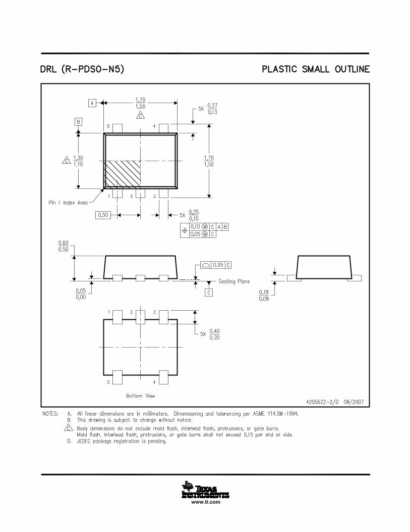
PACKAGE OUTLINE
C
4X 0.270.17
3X 0.320.23
0.4 MAX
0.050.00
2X0.48
0.270.17
0.25 0.1
B 0.850.75
A
0.850.75
(0.1)
(0.06)
4X (0.05) (0.25)
2X (0.26)
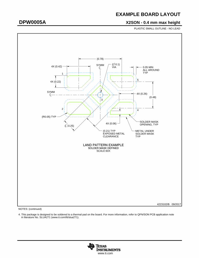
X2SON - 0.4 mm max heightDPW0005APLASTIC SMALL OUTLINE - NO LEAD
4223102/B 09/2017
PIN 1 INDEX AREA
SEATING PLANE
NOTE 3
1
2
3
4
0.1 C A B0.05 C
5
NOTES: 1. All linear dimensions are in millimeters. Any dimensions in parenthesis are for reference only. Dimensioning and tolerancing per ASME Y14.5M. 2. This drawing is subject to change without notice. 3. The size and shape of this feature may vary.
NOTE 3
SCALE 12.000
www.ti.com
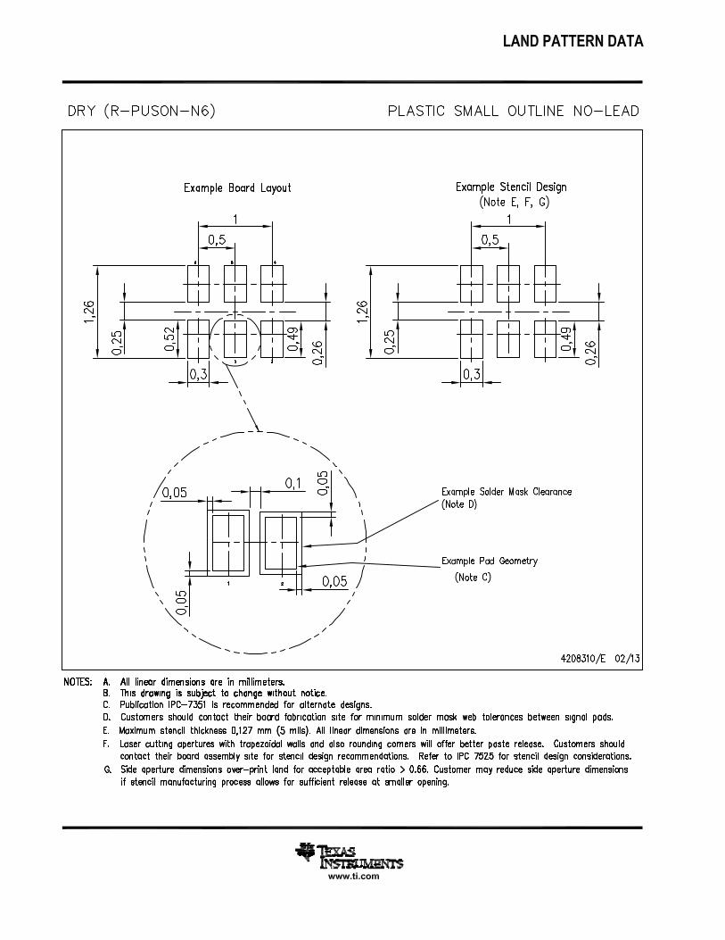
EXAMPLE BOARD LAYOUT
0.05 MINALL AROUNDTYP
(0.21) TYPEXPOSED METALCLEARANCE
(0.48)
(0.78)
4X (0.42)
4X (0.22)
( 0.25)
4X (0.26)
4X (0.06)
( 0.1)VIA
(R0.05) TYP
X2SON - 0.4 mm max heightDPW0005APLASTIC SMALL OUTLINE - NO LEAD
4223102/B 09/2017
SYMM
1
2
3
4
SYMM
LAND PATTERN EXAMPLESOLDER MASK DEFINED
SCALE:60X
SOLDER MASKOPENING, TYP
METAL UNDERSOLDER MASKTYP
5
NOTES: (continued) 4. This package is designed to be soldered to a thermal pad on the board. For more information, refer to QFN/SON PCB application note in literature No. SLUA271 (www.ti.com/lit/slua271).

www.ti.com
EXAMPLE STENCIL DESIGN
(0.48)
(0.78)
4X (0.42)
4X (0.22)
4X (0.26)
4X (0.06)
( 0.24)
(0.21)TYP
(R0.05) TYP
X2SON - 0.4 mm max heightDPW0005APLASTIC SMALL OUTLINE - NO LEAD
4223102/B 09/2017
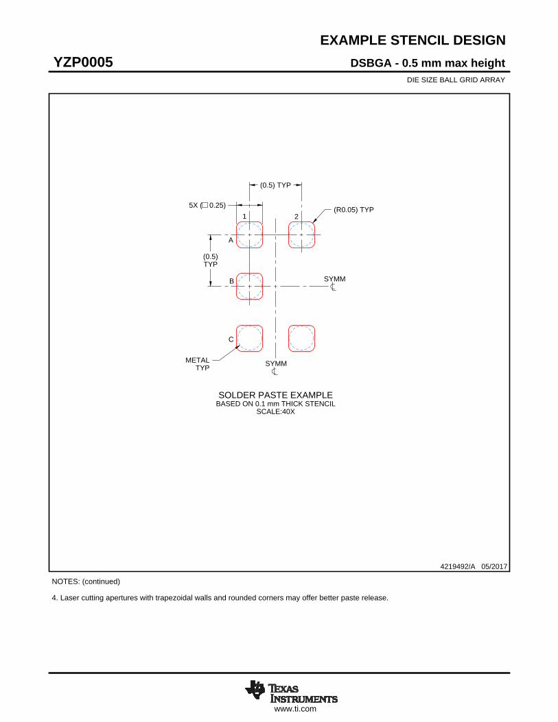
NOTES: (continued) 5. Laser cutting apertures with trapezoidal walls and rounded corners may offer better paste release. IPC-7525 may have alternate design recommendations.
SOLDER PASTE EXAMPLEBASED ON 0.1 mm THICK STENCIL
EXPOSED PAD
92% PRINTED SOLDER COVERAGE BY AREASCALE:100X
SYMM
1
2
3
4
SYMM
EDGESOLDER MASK
5
www.ti.com
PACKAGE OUTLINE
C0.5 MAX
0.190.15
1TYP
0.5 TYP
5X 0.250.21
0.5TYP
B E A
D
4219492/A 05/2017
DSBGA - 0.5 mm max heightYZP0005DIE SIZE BALL GRID ARRAY
NOTES: 1. All linear dimensions are in millimeters. Any dimensions in parenthesis are for reference only. Dimensioning and tolerancing per ASME Y14.5M.2. This drawing is subject to change without notice.
BALL A1CORNER
SEATING PLANE
BALL TYP0.05 C
B
1 2
0.015 C A B
SYMM
SYMM
C
A
SCALE 8.000
D: Max =
E: Max =
1.418 mm, Min =
0.918 mm, Min =
1.358 mm
0.858 mm

www.ti.com
EXAMPLE BOARD LAYOUT
5X ( 0.23)(0.5) TYP
(0.5) TYP
( 0.23)METAL
0.05 MAX ( 0.23)SOLDER MASKOPENING
0.05 MIN
4219492/A 05/2017
DSBGA - 0.5 mm max heightYZP0005DIE SIZE BALL GRID ARRAY
NOTES: (continued) 3. Final dimensions may vary due to manufacturing tolerance considerations and also routing constraints. For more information, see Texas Instruments literature number SNVA009 (www.ti.com/lit/snva009).
SYMM
SYMM
LAND PATTERN EXAMPLESCALE:40X
1 2
A
B
C
NON-SOLDER MASKDEFINED
(PREFERRED)
SOLDER MASK DETAILSNOT TO SCALE
SOLDER MASKOPENING
SOLDER MASKDEFINED
METAL UNDERSOLDER MASK
www.ti.com
EXAMPLE STENCIL DESIGN
(0.5)TYP
(0.5) TYP
5X ( 0.25) (R0.05) TYP
METALTYP
4219492/A 05/2017
DSBGA - 0.5 mm max heightYZP0005DIE SIZE BALL GRID ARRAY
NOTES: (continued) 4. Laser cutting apertures with trapezoidal walls and rounded corners may offer better paste release.
SYMM
SYMM
SOLDER PASTE EXAMPLEBASED ON 0.1 mm THICK STENCIL
SCALE:40X
1 2
A
B
C

www.ti.com
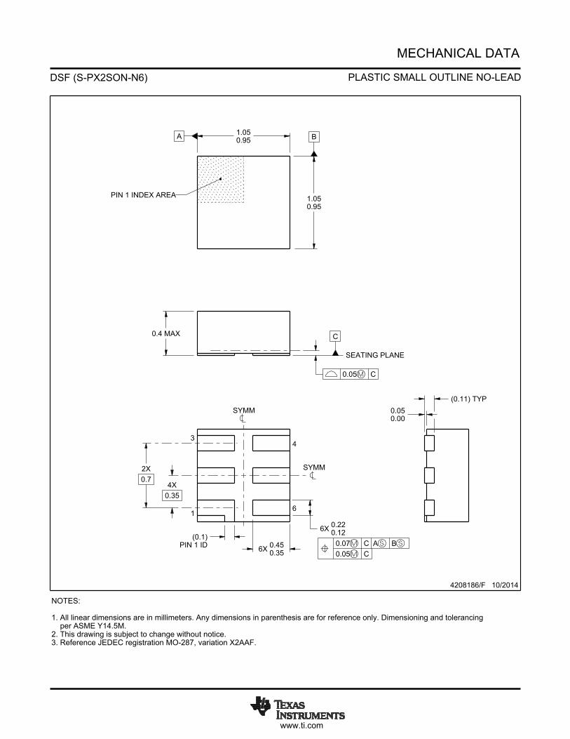
C
6X 0.220.12
6X 0.450.35
2X0.7
4X0.35
0.4 MAX
0.050.00
A 1.050.95 B
1.050.95
(0.11) TYP
(0.1)PIN 1 ID
4208186/F 10/2014
PIN 1 INDEX AREA
SEATING PLANE
0.05 C
1
34
6
0.07 C A B0.05 C
SYMM
SYMM
NOTES: 1. All linear dimensions are in millimeters. Any dimensions in parenthesis are for reference only. Dimensioning and tolerancing per ASME Y14.5M. 2. This drawing is subject to change without notice.3. Reference JEDEC registration MO-287, variation X2AAF.
MECHANICAL DATA
DSF (S-PX2SON-N6) PLASTIC SMALL OUTLINE NO-LEAD


IMPORTANT NOTICE
Texas Instruments Incorporated (TI) reserves the right to make corrections, enhancements, improvements and other changes to itssemiconductor products and services per JESD46, latest issue, and to discontinue any product or service per JESD48, latest issue. Buyersshould obtain the latest relevant information before placing orders and should verify that such information is current and complete.TI’s published terms of sale for semiconductor products (http://www.ti.com/sc/docs/stdterms.htm) apply to the sale of packaged integratedcircuit products that TI has qualified and released to market. Additional terms may apply to the use or sale of other types of TI products andservices.Reproduction of significant portions of TI information in TI data sheets is permissible only if reproduction is without alteration and isaccompanied by all associated warranties, conditions, limitations, and notices. TI is not responsible or liable for such reproduceddocumentation. Information of third parties may be subject to additional restrictions. Resale of TI products or services with statementsdifferent from or beyond the parameters stated by TI for that product or service voids all express and any implied warranties for theassociated TI product or service and is an unfair and deceptive business practice. TI is not responsible or liable for any such statements.Buyers and others who are developing systems that incorporate TI products (collectively, “Designers”) understand and agree that Designersremain responsible for using their independent analysis, evaluation and judgment in designing their applications and that Designers havefull and exclusive responsibility to assure the safety of Designers' applications and compliance of their applications (and of all TI productsused in or for Designers’ applications) with all applicable regulations, laws and other applicable requirements. Designer represents that, withrespect to their applications, Designer has all the necessary expertise to create and implement safeguards that (1) anticipate dangerousconsequences of failures, (2) monitor failures and their consequences, and (3) lessen the likelihood of failures that might cause harm andtake appropriate actions. Designer agrees that prior to using or distributing any applications that include TI products, Designer willthoroughly test such applications and the functionality of such TI products as used in such applications.TI’s provision of technical, application or other design advice, quality characterization, reliability data or other services or information,including, but not limited to, reference designs and materials relating to evaluation modules, (collectively, “TI Resources”) are intended toassist designers who are developing applications that incorporate TI products; by downloading, accessing or using TI Resources in anyway, Designer (individually or, if Designer is acting on behalf of a company, Designer’s company) agrees to use any particular TI Resourcesolely for this purpose and subject to the terms of this Notice.TI’s provision of TI Resources does not expand or otherwise alter TI’s applicable published warranties or warranty disclaimers for TIproducts, and no additional obligations or liabilities arise from TI providing such TI Resources. TI reserves the right to make corrections,enhancements, improvements and other changes to its TI Resources. TI has not conducted any testing other than that specificallydescribed in the published documentation for a particular TI Resource.Designer is authorized to use, copy and modify any individual TI Resource only in connection with the development of applications thatinclude the TI product(s) identified in such TI Resource. NO OTHER LICENSE, EXPRESS OR IMPLIED, BY ESTOPPEL OR OTHERWISETO ANY OTHER TI INTELLECTUAL PROPERTY RIGHT, AND NO LICENSE TO ANY TECHNOLOGY OR INTELLECTUAL PROPERTYRIGHT OF TI OR ANY THIRD PARTY IS GRANTED HEREIN, including but not limited to any patent right, copyright, mask work right, orother intellectual property right relating to any combination, machine, or process in which TI products or services are used. Informationregarding or referencing third-party products or services does not constitute a license to use such products or services, or a warranty orendorsement thereof. Use of TI Resources may require a license from a third party under the patents or other intellectual property of thethird party, or a license from TI under the patents or other intellectual property of TI.TI RESOURCES ARE PROVIDED “AS IS” AND WITH ALL FAULTS. TI DISCLAIMS ALL OTHER WARRANTIES ORREPRESENTATIONS, EXPRESS OR IMPLIED, REGARDING RESOURCES OR USE THEREOF, INCLUDING BUT NOT LIMITED TOACCURACY OR COMPLETENESS, TITLE, ANY EPIDEMIC FAILURE WARRANTY AND ANY IMPLIED WARRANTIES OFMERCHANTABILITY, FITNESS FOR A PARTICULAR PURPOSE, AND NON-INFRINGEMENT OF ANY THIRD PARTY INTELLECTUALPROPERTY RIGHTS. TI SHALL NOT BE LIABLE FOR AND SHALL NOT DEFEND OR INDEMNIFY DESIGNER AGAINST ANY CLAIM,INCLUDING BUT NOT LIMITED TO ANY INFRINGEMENT CLAIM THAT RELATES TO OR IS BASED ON ANY COMBINATION OFPRODUCTS EVEN IF DESCRIBED IN TI RESOURCES OR OTHERWISE. IN NO EVENT SHALL TI BE LIABLE FOR ANY ACTUAL,DIRECT, SPECIAL, COLLATERAL, INDIRECT, PUNITIVE, INCIDENTAL, CONSEQUENTIAL OR EXEMPLARY DAMAGES INCONNECTION WITH OR ARISING OUT OF TI RESOURCES OR USE THEREOF, AND REGARDLESS OF WHETHER TI HAS BEENADVISED OF THE POSSIBILITY OF SUCH DAMAGES.Unless TI has explicitly designated an individual product as meeting the requirements of a particular industry standard (e.g., ISO/TS 16949and ISO 26262), TI is not responsible for any failure to meet such industry standard requirements.Where TI specifically promotes products as facilitating functional safety or as compliant with industry functional safety standards, suchproducts are intended to help enable customers to design and create their own applications that meet applicable functional safety standardsand requirements. Using products in an application does not by itself establish any safety features in the application. Designers mustensure compliance with safety-related requirements and standards applicable to their applications. Designer may not use any TI products inlife-critical medical equipment unless authorized officers of the parties have executed a special contract specifically governing such use.Life-critical medical equipment is medical equipment where failure of such equipment would cause serious bodily injury or death (e.g., lifesupport, pacemakers, defibrillators, heart pumps, neurostimulators, and implantables). Such equipment includes, without limitation, allmedical devices identified by the U.S. Food and Drug Administration as Class III devices and equivalent classifications outside the U.S.TI may expressly designate certain products as completing a particular qualification (e.g., Q100, Military Grade, or Enhanced Product).Designers agree that it has the necessary expertise to select the product with the appropriate qualification designation for their applicationsand that proper product selection is at Designers’ own risk. Designers are solely responsible for compliance with all legal and regulatoryrequirements in connection with such selection.Designer will fully indemnify TI and its representatives against any damages, costs, losses, and/or liabilities arising out of Designer’s non-compliance with the terms and provisions of this Notice.
Mailing Address: Texas Instruments, Post Office Box 655303, Dallas, Texas 75265Copyright © 2018, Texas Instruments Incorporated