Embed Size (px)
Citation preview

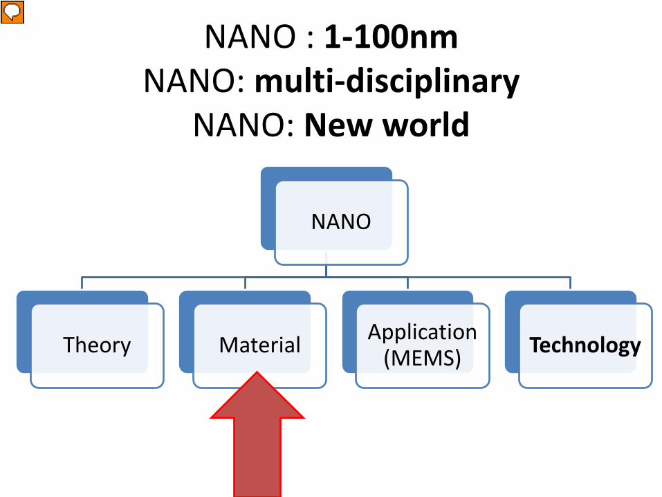
NANO
Science·Material·Application·Technology
段力
2015.4

Out line
• NANO = Science + Material + Application + Technology
• NANO – the future

NANO
Theory Material Application (MEMS) Technology
NANO : 1-100nmNANO: multi-disciplinary
NANO: New world

NANO in a glance
• NANO is:
– NANO is the study of 1-100 nm range
– NANO is a multi-disciplinary
– NANO opens a new world
• 4 main aspects:
– Science / theory– Material– Application– Technology

NANO: Science
• Multi-discipline• Physics + Chemistry + Biology + ··· + IC Technology
• Computer simulation: • Models:Multi-physics, Poisson equation, Schrodinger
equation• Application: Quantum structures, 3D, MEMS• Tools: COMSOL,Pisces, ATLAS , Cadence
NANO
Theory Material Application (MEMS) Technology
NANO : 1-100nmNANO: multi-disciplinary
NANO: New world

Nano Material
• 什么是纳米材料?有人简称为0D,1D,2D,3D, 也就是至少在一个维度上,尺度在1nm –0.1mm之间的材料。
• 纳米点、纳米线、薄膜、纳米粉体颗粒\纤维(比表面积大, specific surface area (SSA),100-1000 m^2/g)

NANO: Material
• Nanometer material may have distinct physical / chemical / etc, behaviors, Such as carbon nanotube (CNT), gold, Si/SiO2 and various hetero junction interface

NANO: Material - thin film
• Most of the devices just use the top layers (~um) to fulfill their functions,
• expensive substrate is a waste, – 例子。SOI, 镀金的首饰。
• Thin film technology offers a cheaper way to make use of various expensive bulk materials
• 薄膜技术:微电子技术为引进新材料带来可能
– 硅衬底 + 薄膜:Au, Ti, IIIV, IIVI, 锗, SOI, HKMG, Salicide, Cu , Low K,...

NANO: Material -酒瓶新酒
• 同一个元素\不同的视角
– 门捷列夫与微纳米,同一种原子、分子,不同的组合方式 =》
– 例如,C材料, 之前只有石墨和金刚石, 现在有了石墨烯和碳纳米管。它们的元素符号都是c。但是由于组合的不同,就形成了新的物质。

Nano:material→ C
• 金刚石 + 石墨 +富勒烯C60,
• 石墨烯 + 碳纳米管(英文Carbon Nanotube,缩写CNT)日本物理学家饭岛澄男(Iijima Sumio )

C -石墨烯(Graphene)

C- CNT
• 碳纳米管
英文Carbon Nanotube,缩写CNT日本物理学家饭岛澄男( Iijima Sumio )

再下边材料就应该是

NANO
Theory Material Application (MEMS) Technology
NANO : 1-100nmNANO: multi-disciplinary
NANO: New world

Nano:Applications• MEMS
– MEMS (Micro Electro Mechanical System)– Sensors, actuators
• New Devices:– CNT – man-made material– CNT transistors, CNTFET
• Energy, chemistry, civil:– Lotus effect – very high water repellence of the leaves of the lotus flower– Catalyst – Fuel cell
• ... ...

Nano:Applications→MEMS
• MEMS / SOC
– E: IC as a brain, M: as a hand.
– Sensor is to receive; actuator is to response
– Technology:borrow the IC technology
【 From/to 】 Temperature, optical, mechanical, chemical, magnetic signals【To/from】An electrical signal

Nano:Applications→出淤泥而不染
• 周敦颐《爱莲说》「莲花出淤泥而不染」为什么呢?
• Lotus Effect 莲之所以出淤泥而不染的原因是莲叶的表面奈米结构达到自洁的效果,如
此表面自我洁净的物理现象称为『莲叶效应』!
• 科学家们模拟莲叶的表面,发明了纳米自清洁的衣料和建筑涂料,只需一点水形成水滴,就可以自动清洁衣物和建筑表面。

NANO
Theory Material Application (MEMS) Technology
NANO : 1-100nmNANO: multi-disciplinary
NANO: New world

Nano Technology
• Most from IC industry• 4 basic steps (repeating)
– Draw– Add– Remove– Modify

Nano Technology
• Draw – using photolithography to draw a pattern of pictures
• Light, exposing• Mask, patterning
• Paint – using the pattern to add, remove or change the material selectively
• Add: thin film deposition, epitaxy, thermal growth, • Remove: wet etching, plasma etching, CMP• Modify: ion implantation, alloying, saliciding

Micro/nano process
• 在薄膜淀积之后,
• 在表面涂一层光刻胶(PR),然后光线(Light)透过光刻版(Mask)对硅片进行曝光(Light Exposure)、显影(Developing)、烘干(Baking)
• 之后进行刻蚀(Etching),
• 除去光刻胶之后,就在薄膜上得到了所需要的图案

Micro/nano process
Light Exposure
Developing
Etching
PR Stripping
Light Exposure
Developing
Light Exposure
Etching
Developing
Light Exposure
PR Stripping
Etching
Developing
Light ExposureLight Exposure
Developing
Etching
PR Stripping
Mask
Light Exposure
Developing
Light Exposure
Etching
Developing
Light Exposure
PR Stripping
Etching
Developing
Light Exposure
Light
Feature Size Lithography Wavelength
365nm
248nm
193nm
180nm
90nm 45nmSubstrate
Thickness
GapWidth
photoresist
Substrate
Thickness
Width Gap
PhotoresistPhotoresist
Feature Size Lithography Wavelength
365nm
248nm
193nm
180nm
90nm 45nmSubstrate
Thickness
GapWidth
photoresist
Substrate
Thickness
Width Gap
PhotoresistPhotoresist
(a) (b)

Nano Technology: Photolithography
Reducing the size for the
past 30 years

CostYield
More function
Reducing the size , why?
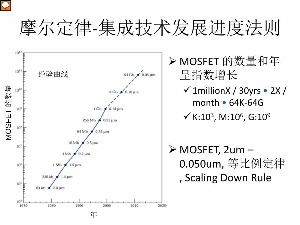
摩尔定律-集成技术发展进度法则
MOSFET 的数量和年呈指数增长
1millionX / 30yrs • 2X / month • 64K-64G
K:103, M:106, G:109
MOSFET, 2um –0.050um, 等比例定律, Scaling Down Rule
年
MO
SFET
的数量
经验曲线

Nano Technology: Thin film deposition
• Methods:– PVD, CVD– Epitaxy– Thermal
• Criteria:– Uniformity, quality, defects, step coverage, deposition
rate• Materials:
– Base material, Si– Optical (LED, Solar) ,Magnetic (Compass), Stress
(Strained Si)

ALD: delicate thin film growth
Better thickness control Better 3D coverage

Nano Technology: etching
【Wet etching】easy, hard to control lateral【Dry etching】ion + chemical, < 0.1um patterning 【Damascene】CMP, hard to etch Cu, Metal Gate
【3D Shaping】Σ shape patterning, SiGe
isotropic vs. anisotropic, {111} < {110} < {100},
selectivity, etch rate,

Nano Technology: modify the material
• Ion implantation, annealing• Salicide, sputtering, alloying• Post processing
– FPGA– Flash – ROM, Fuse, anti-fuse

FEOL: smaller and smaller “T”s
Si Substrate
Poly SiSi3N4
Buffer Oxide
Silacide
Silacide

BEOL more and more “L”s
Contact
M1 Oxide
Via
M2
Cu
SEM of Copper Interconnect
Nitride
Si
ILD淀积/刻沟
Cu淀积
CMP磨平

Out line
• NANO = Science + Material + Application + Technology
• NANO - future trend
Nano trend
• Longer: 长度方向:科研
– 新的纳米材料(0D、1D、2D),人造材料
– 新的纳米物理、原理
– 新的纳米器件、新纳米结构
– MEMS
• Wider: 宽度方向:应用
– 利用现有的微纳技术进行跨学科的应用

Longer:physics
• 新材料
– 启发,用最便宜的材料,做成最不平凡的事,就是使用自然界常用、便宜的材料,来造成革命性的变革。
1. 首先是Si,就是沙子,造成了现在的信息革命。
2. 然后是C,就是木头。碳:金刚石+石墨+C60+grephene+CNT,同一种原子、分子,不同的组合方式 =》新的材料,旧瓶装新酒。
3. 然后是 H2O,水里面的内容是很多的,不仅包含了物质层次,也包含了意识层次。
• 新器件、新原理
• 新结构、MEMS

Wider:应用
基本思路,科技人人白日梦。也就是将自己的所长、技术与经历用于要用的领域 。
这张图是2006年时候的图。那个时候图里面的这些东西还都是分立的元件。现在,他们都已经被集成了,就是现在我们的智能手机。

Summary
• Nano is a multidicipilinary of Physics + Chemistry + Biology + nano Engineering
• Nano has 4 main aspects: Science, Material, Application and Technology
• 3 main nanotechnologies :photolithography, etching, and thin film, in the playground of nano/MEMS fabrication.
• MEMS + SOC may offer a large application and market place to play.
习题
• Nano的4个方面?
• Nano 跨学科?几个学科?
• Nano Technology 的4个基本工艺?
• “加法的”几种方法?
• “减法的”几种方法?
• Micro/nano process 的示意图?
• 缩减光刻尺寸对微纳工艺集成电路发展的三项基本贡献?
• 微纳学的未来发展的两种方向?

FIN
Thank you!