Embed Size (px)
Citation preview

Timers
11
Section 11. Timers
HIGHLIGHTSThis section of the manual contains the following topics:
11.1 Introduction ................................................................................................................. 11-211.2 Timer Variants ............................................................................................................. 11-311.3 Control Registers ........................................................................................................ 11-611.4 Modes of Operation................................................................................................... 11-1011.5 Timer Interrupts ......................................................................................................... 11-1511.6 32-Bit Timer Configuration ........................................................................................ 11-1611.7 32-Bit Timer Modes of Operation .............................................................................. 11-1811.8 Timer Operation in Power-Saving Modes ................................................................. 11-2011.9 Peripherals Using Timer Modules ............................................................................. 11-2111.10 Register Maps ........................................................................................................... 11-2211.11 Related Application Notes......................................................................................... 11-2411.12 Revision History ........................................................................................................ 11-25
© 2010 Microchip Technology Inc. DS70362B-page 11-1

dsPIC33E/PIC24E Family Reference Manual
11.1 INTRODUCTIONThe dsPIC33E/PIC24E device family offers several 16-bit timer modules. With certainexceptions, all of the 16-bit timers have the same functional circuitry, and are classified into threetypes according to their functional differences:
• Type A timer (Timer1)• Type B timer (Timer2, Timer4, Timer6 and Timer8)• Type C timer (Timer3, Timer5, Timer7 and Timer9)
The Type B and Type C timers can be combined to form a 32-bit timer.
Each timer module is a 16-bit timer/counter consisting of the following readable/writableregisters:
• TMRx: 16-bit Timer Count register• PRx: 16-bit Timer Period register associated with the timer• TxCON: 16-bit Timer Control register associated with the timer
Each timer module also has these associated bits for interrupt control:
• Interrupt Enable Control bit (TxIE)• Interrupt Flag Status bit (TxIF)• Interrupt Priority Control bits (TxIP<2:0>)
Note: This family reference manual section is meant to serve as a complement to devicedata sheets. Depending on the device variant, this manual section may not applyto all dsPIC33E/PIC24E devices.
Please consult the note at the beginning of the “Timers” chapter in the currentdevice data sheet to check whether this document supports the device you areusing.
Device data sheets and family reference manual sections are available fordownload from the Microchip Worldwide Web site at: http://www.microchip.com
Note 1: Each dsPIC33E/PIC24E device variant can have one or more timer modules. Formore information, refer to the specific device data sheet.
2: An ‘x’ used in the names of pins, control/status bits and registers denotes theparticular timer number (x = 1 to 9).
3: A ‘y’ used in the names of pins, control/status bits and registers denotes the particular Type C timer number (y = 3, 5, 7, and 9).
DS70362B-page 11-2 © 2010 Microchip Technology Inc.

Section 11. TimersTim
ers
11
11.2 TIMER VARIANTSThis section describes the different types of timers available on the dsPIC33E/PIC24E family ofdevices.
11.2.1 Type A TimerTimer1 is a Type A timer. The Type A timer has the following unique features over other types oftimers:
• Can be operated from the low-power 32 kHz crystal oscillator available on the device• Can be operated in Asynchronous Counter mode from an external clock source• Optionally, the external clock input (TxCK) can be synchronized to the internal device clock
and clock synchronization is performed after TxCK is divided by the prescaler. The advantage of clock synchronization after division by the prescaler is explained in the Section 11.4.3 “Synchronous Counter Mode”.
The unique features of a Type A timer allow it to be used for Real Time Clock (RTC) applications.Figure 11-1 illustrates a block diagram of a Type A timer.
Figure 11-1: Type A Timer Block Diagram
TGATE
TCS
00
10
x1
TMRx
Comparator
TGATE
Set TxIF flag
0
1
TSYNC
0
1
Sync
SOSCI
SOSCO/T1CK
Prescaler(/n)
TCKPS<1:0>
GateSync
FCY(1)
Falling Edge Detect
Prescaler(/n)
TCKPS<1:0>
LPOSCEN(2)
Note 1: FCY is the instruction cycle clock.2: For more information on secondary oscillator, refer to Section 7. “Oscillator” (DS70580).
Timer Sync
T1CK
Latch
Out
TON
Data
Equal
CLK
Reset
PRx
© 2010 Microchip Technology Inc. DS70362B-page 11-3

dsPIC33E/PIC24E Family Reference Manual
11.2.2 Type B TimerTimer2, Timer4, Timer6 and Timer8, if present, are Type B timers. The Type B timer has thefollowing specific features:
• It can be concatenated with a Type C timer to form a 32-bit timer• The external clock input (TxCK) is always synchronized to the internal device clock and
clock synchronization is performed after TxCK is divided by the prescaler. The advantage of clock synchronization after division by the prescaler is explained in 11.4.3 “Synchronous Counter Mode”
Figure 11-2 illustrates a block diagram of the Type B timer.
Figure 11-2: Type B Timer Block Diagram
Prescaler(/n)
TGATE
TCS
00
10
x1
TGATE
Set TxIF flag
0
1
Sync
TCKPS<1:0>
TxCK
GateSync
FCY(1)
Falling Edge Detect
Prescaler(/n)
TCKPS<1:0>
Note 1: FCY is the instruction cycle clock.
TMRx
Comparator
Timer Sync
Latch
OutTON
Data
Equal
CLK
Reset
PRx
DS70362B-page 11-4 © 2010 Microchip Technology Inc.

Section 11. TimersTim
ers
11
11.2.3 Type C TimerTimer3, Timer5, Timer7 and Timer9, if present, are Type C timers. The Type C timer has the following specific features:• It can be concatenated with a Type B timer to form a 32-bit timer• At least one Type C timer has the ability to trigger an Analog-to-Digital (A/D) conversion • The external clock input (TxCK) is always synchronized to the internal device clock and the
clock synchronization is performed using TxCK, after which this synchronized clock is divided by the prescaler
Figure 11-3 illustrates a block diagram of the Type C timer.
Figure 11-3: Type C Timer Block Diagram
Prescaler
GateSync
TGATE
TCS
00
10
x1
FCY(1)
TGATE
Falling Edge Detect Set TxIF flag
0
1
Sync
TCKPS<1:0>
TxCK
ADC SOC Trigger(2)
Prescaler(/n)
TCKPS<1:0>
Note 1: FCY is the instruction cycle clock.2: ADC trigger is available only on TMR3 and TMR5.
TMRx
Comparator
Timer Sync
Latch
OutTON
Data
Equal
CLK
Reset
PRx
(/n)
© 2010 Microchip Technology Inc. DS70362B-page 11-5

dsPIC33E/PIC24E Family Reference Manual
11.3 CONTROL REGISTERSThis section outlines the functions of specific timer control registers.
• TxCON: Type A Timer Control Register (x = 1)This register controls the configuration of a Type A timer.
• TxCON: Type B Timer Control Register (x = 2, 4, 6, 8)This register controls the configuration of a Type B timer.
• TxCON: Type C Timer Control Register (x = 3, 5, 7, 9)This register controls the configuration of a Type C timer.
In addition to the above registers, each timer has the following 16-bit registers associated with it.
• PRx: Timer Period Register (x = 1 through 9)
This is the 16-bit timer period register.
• TMRx: Timer Count Register (x = 1 through 9)
This is the 16-bit timer count register.
• TMRxHLD: Timer Hold Register (x = 3, 5, 7, and 9)
This register is used in 32-bit Timer mode read/write operations.
DS70362B-page 11-6 © 2010 Microchip Technology Inc.

Section 11. TimersTim
ers
11
Register 11-1: TxCON: Type A Timer Control Register (x = 1)
R/W-0 U-0 R/W-0 U-0 U-0 U-0 U-0 U-0TON — TSIDL — — — — —
bit 15 bit 8
U-0 R/W-0 R/W-0 R/W-0 U-0 R/W-0 R/W-0 U-0— TGATE TCKPS<1:0> — TSYNC TCS —
bit 7 bit 0
Legend:R = Readable bit W = Writable bit U = Unimplemented bit, read as ‘0’-n = Value at POR ‘1’ = Bit is set ‘0’ = Bit is cleared x = Bit is unknown
bit 15 TON: Timer On bit1 = Starts the timer0 = Stops the timer
bit 14 Unimplemented: Read as ‘0’bit 13 TSIDL: Stop in Idle Mode bit
1 = Discontinue timer operation when device enters Idle mode0 = Continue timer operation in Idle mode
bit 12-7 Unimplemented: Read as ‘0’bit 6 TGATE: Timer Gated Time Accumulation Enable bit
When TCS = 1:This bit is ignoredWhen TCS = 0:1 = Gated time accumulation enabled0 = Gated time accumulation disabled
bit 5-4 TCKPS<1:0>: Timer Input Clock Prescale Select bits11 = 1:256 prescale value10 = 1:64 prescale value01 = 1:8 prescale value00 = 1:1 prescale value
bit 3 Unimplemented: Read as ‘0’bit 2 TSYNC: Timer External Clock Input Synchronization Select bit
When TCS = 1: 1 = Synchronize external clock input0 = Do not synchronize external clock inputWhen TCS = 0: This bit is ignored. Read as ‘0’. Timer uses the internal clock when TCS = 0
bit 1 TCS: Timer Clock Source Select bit1 = External clock from TxCK pin (on the rising edge), also used as a clock request to SOSC0 = Internal clock (FOSC/2)
bit 0 Unimplemented: Read as ‘0’
© 2010 Microchip Technology Inc. DS70362B-page 11-7

dsPIC33E/PIC24E Family Reference Manual
Register 11-2: TxCON: Type B Timer Control Register (x = 2, 4, 6, 8)
R/W-0 U-0 R/W-0 U-0 U-0 U-0 U-0 U-0TON — TSIDL — — — — —
bit 15 bit 8
U-0 R/W-0 R/W-0 R/W-0 R/W-0 U-0 R/W-0 U-0— TGATE TCKPS<1:0> T32 — TCS —
bit 7 bit 0
Legend:R = Readable bit W = Writable bit U = Unimplemented bit, read as ‘0’-n = Value at POR ‘1’ = Bit is set ‘0’ = Bit is cleared x = Bit is unknown
bit 15 TON: Timerx On bitWhen T32 = 1 (in 32-bit Timer mode):1 = Starts 32-bit TMRy(1):TMRx timer pair0 = Stops 32-bit TMRy(1):TMRx timer pairWhen T32 = 0 (in 16-bit Timer mode):1 = Starts 16-bit timer0 = Stops 16-bit timer
bit 14 Unimplemented: Read as ‘0’bit 13 TSIDL: Stop in Idle Mode bit
1 = Discontinue timer operation when device enters Idle mode0 = Continue timer operation in Idle mode
bit 12-7 Unimplemented: Read as ‘0’bit 6 TGATE: Timerx Gated Time Accumulation Enable bit
When TCS = 1:This bit is ignoredWhen TCS = 0:1 = Gated time accumulation enabled0 = Gated time accumulation disabled
bit 5-4 TCKPS<1:0>: Timerx Input Clock Prescale Select bits11 = 1:256 prescale value10 = 1:64 prescale value01 = 1:8 prescale value00 = 1:1 prescale value
bit 3 T32: 32-Bit Timerx Mode Select bit1 = TMRx and TMRy(1) form a 32-bit timer0 = TMRx and TMRy(1) form separate 16-bit timer
bit 2 Unimplemented: Read as ‘0’bit 1 TCS: Timerx Clock Source Select bit
1 = External clock from TxCK pin (on the rising edge)0 = Internal clock (FOSC/2)
bit 0 Unimplemented: Read as ‘0’
Note 1: TMRy is a Type C timer (y = 3, 5, 7, and 9)
DS70362B-page 11-8 © 2010 Microchip Technology Inc.

Section 11. TimersTim
ers
11
Register 11-3: TxCON: Type C Timer Control Register (x = 3, 5, 7, 9)
R/W-0 U-0 R/W-0 U-0 U-0 U-0 U-0 U-0TON(2) — TSIDL(1) — — — — —
bit 15 bit 8
U-0 R/W-0 R/W-0 R/W-0 U-0 U-0 R/W-0 U-0— TGATE(2) TCKPS<1:0>(2) — — TCS(2) —
bit 7 bit 0
Legend:R = Readable bit W = Writable bit U = Unimplemented bit, read as ‘0’-n = Value at POR ‘1’ = Bit is set ‘0’ = Bit is cleared x = Bit is unknown
bit 15 TON: Timerx On bit(2)
1 = Starts 16-bit Timerx0 = Stops 16-bit Timerx
bit 14 Unimplemented: Read as ‘0’bit 13 TSIDL: Stop in Idle Mode bit (1)
1 = Discontinue timer operation when device enters Idle mode0 = Continue timer operation in Idle mode
bit 12-7 Unimplemented: Read as ‘0’bit 6 TGATE: Timerx Gated Time Accumulation Enable bit(2)
When TCS = 1:This bit is ignoredWhen TCS = 0:1 = Gated time accumulation enabled0 = Gated time accumulation disabled
bit 5-4 TCKPS<1:0>: Timerx Input Clock Prescale Select bits(2)
11 = 1:256 prescale value10 = 1:64 prescale value01 = 1:8 prescale value00 = 1:1 prescale value
bit 3-2 Unimplemented: Read as ‘0’bit 1 TCS: Timerx Clock Source Select bit(2)
1 = External clock from TxCK pin (on the rising edge)0 = Internal clock (FOSC/2)
bit 0 Unimplemented: Read as ‘0’
Note 1: When 32-bit timer operation is enabled (T32 = 1) in Type B Timer Control (TxCON<3>) register, TSIDL bitmust be cleared to operate the 32-bit timer in Idle mode.
2: These bits have no effect when the 32-bit timer operation is enabled (T32 = 1) in the Type B Timer Control(TxCON<3>) register.
© 2010 Microchip Technology Inc. DS70362B-page 11-9
dsPIC33E/PIC24E Family Reference Manual
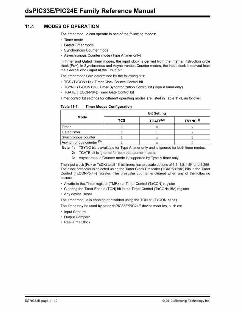
11.4 MODES OF OPERATIONThe timer module can operate in one of the following modes:
• Timer mode• Gated Timer mode• Synchronous Counter mode• Asynchronous Counter mode (Type A timer only)
In Timer and Gated Timer modes, the input clock is derived from the internal instruction cycleclock (FCY). In Synchronous and Asynchronous Counter modes, the input clock is derived fromthe external clock input at the TxCK pin.
The timer modes are determined by the following bits:
• TCS (TxCON<1>): Timer Clock Source Control bit• TSYNC (TxCON<2>): Timer Synchronization Control bit (Type A timer only)• TGATE (TxCON<6>): Timer Gate Control bit
Timer control bit settings for different operating modes are listed in Table 11-1, as follows:
The input clock (FCY or TxCK) to all 16-bit timers has prescale options of 1:1, 1:8, 1:64 and 1:256.The clock prescaler is selected using the Timer Clock Prescaler (TCKPS<1:0>) bits in the TimerControl (TxCON<5:4>) register. The prescaler counter is cleared when any of the followingoccurs:
• A write to the Timer register (TMRx) or Timer Control (TxCON) register• Clearing the Timer Enable (TON) bit in the Timer Control (TxCON<15>) register • Any device Reset
The timer module is enabled or disabled using the TON bit (TxCON <15>).
The timer may be used by other dsPIC33E/PIC24E device modules, such as:
• Input Capture• Output Compare• Real-Time Clock
Table 11-1: Timer Modes Configuration
ModeBit Setting
TCS TGATE(2) TSYNC(1)
Timer 0 0 x
Gated timer 0 1 xSynchronous counter 1 x 1
Asynchronous counter (3) 1 x 0
Note 1: TSYNC bit is available for Type A timer only and is ignored for both timer modes.2: TGATE bit is ignored for both the counter modes.3: Asynchronous Counter mode is supported by Type A timer only.
DS70362B-page 11-10 © 2010 Microchip Technology Inc.

Section 11. TimersTim
ers
11
11.4.1 Timer ModeIn Timer mode, the input clock to the timer is derived from the internal clock (FCY), divided by aprogrammable prescaler. When the timer is enabled, it increments by one on every rising edgeof the input clock and generates an interrupt on a period match. Figure 11-4 illustrates the timeroperation.To configure Timer mode:
1. Clear the TCS control bit (TxCON<11>) to select the internal clock source.2. Clear the TGATE control bit (TxCON<6>) to disable Gated Timer mode operation.
Setting the TSYNC bit (TxCON<2>) has no effect because the internal clock is alwayssynchronized.
Example 11-1 provides the code sequence to set up Timer1 in 16-bit Timer mode. This codegenerates an interrupt on every 10 cycles of the timer input clock.
Example 11-1: Initialization Code for 16-bit Timer Mode
Figure 11-4: Interrupt Timing for Timer Period Match
T1CONbits.TON = 0; // Disable TimerT1CONbits.TCS = 0; // Select internal instruction cycle clock T1CONbits.TGATE = 0; // Disable Gated Timer modeT1CONbits.TCKPS = 0b011; // Select 1:8 PrescalerTMR1 = 0x00; // Clear timer registerPR1 = 9; // Load the period value
IPC0bits.T1IP = 0x01; // Set Timer 1 Interrupt Priority LevelIFS0bits.T1IF = 0; // Clear Timer 1 Interrupt FlagIEC0bits.T1IE = 1; // Enable Timer1 interrupt
T1CONbits.TON = 1; // Start Timer
/* Example code for Timer1 ISR*/void __attribute__((__interrupt__, no_auto_psv)) _T1Interrupt(void){/* Interrupt Service Routine code goes here */
IFS0bits.T1IF = 0; //Clear Timer1 interrupt flag}
TimerClockInput
TxIF
TMRx 1 2 3 4 0 1 2 3 4 5 6 7 0 1 2 30
PRx 9
Cleared by user software Cleared by user software
8 95 6 7 8 9
~ ~ ~ ~
1 TCY 1 TCY
© 2010 Microchip Technology Inc. DS70362B-page 11-11

dsPIC33E/PIC24E Family Reference Manual
11.4.2 Gated Timer ModeWhen the timer module operates with the internal clock (TCS = 0), Gated Timer mode can beused to measure the duration of an external gate signal. In this mode, the timer increments byone on every rising edge of the input clock as long as the external gate signal at the TxCK pin ishigh. The timer interrupt is generated on the falling edge of the TxCK pin. Figure 11-5 illustratesGated Timer mode operation. To configure the Gated Timer mode:1. Set the TGATE control bit (TxCON<6>) to enable gated timer operation.2. Clear the TCS control bit (TxCON<11>) to select the internal clock source.Setting the TSYNC bit (TxCON<2>) has no effect because the internal clock is alwayssynchronized.Example 11-2 provides the code sequence to measure pulse width (T1CK) in Gated Timer mode.
Example 11-2: Initialization Code for 16-bit Gated Timer Mode
Figure 11-5: Gated Timer Mode Operation
T1CONbits.TON = 0; // Disable TimerT1CONbits.TCS = 0; // Select internal instruction cycle clock T1CONbits.TGATE = 1; // Enable Gated Timer modeT1CONbits.TCKPS = 0b00; // Select 1:1 PrescalerTMR1 = 0x00; // Clear timer registerPR1 = 9; // Load the period value
IPC0bits.T1IP = 0x01; // Set Timer 1 Interrupt Priority LevelIFS0bits.T1IF = 0; // Clear Timer 1 Interrupt FlagIEC0bits.T1IE = 1; // Enable Timer1 interrupt
T1CONbits.TON = 1; // Start Timer
/* Example code for Timer1 ISR*/void __attribute__((__interrupt__, no_auto_psv)) _T1Interrupt(void){/* Interrupt Service Routine code goes here */
IFS0bits.T1IF = 0; //Clear Timer1 interrupt flag}
Timer Clock Input
(Internal)
TxIF
TMRx 1 2 3 8 90
PRx 9
Cleared by user software Cleared by user software
TxCK(Gate Input)
4 5 6 7 1 20
DS70362B-page 11-12 © 2010 Microchip Technology Inc.

Section 11. TimersTim
ers
11
11.4.3 Synchronous Counter ModeIn Synchronous Counter mode, the input clock to the timer is derived from the external clock inputdivided by a programmable prescaler. In this mode, the external clock input is synchronized withthe internal device clock. When the timer is enabled, it increments by one on every rising edgeof the input clock, and generates an interrupt on a period match.To configure Synchronous Counter mode:
• Set the TSYNC control bit (TxCON<2>) for a Type A timer to enable clock synchronization. For a Type B or Type C timer, the external clock input is always synchronized.
• Set the TCS control bit (TxCON<1>) to select the external clock source.
A timer operating from a synchronized external clock source does not operate in Sleep mode,because the synchronization circuit is shut off during Sleep mode.
For Type C timers, it is necessary for the external clock input period to be high for at least 0.5 TCY(and an additional input buffer delay of 20 ns), and low for at least 0.5 TCY (and an additional inputbuffer delay of 20 ns) for proper synchronization.
The clock synchronization for a Type A and Type B timer is performed after the prescaler and theprescaler output changes on the rising edge of the input. Therefore, for a Type A and Type Btimer, the external clock input period must be at least 0.5 TCY (and an additional input buffer delayof 20 ns) divided by the prescaler value.
However, the high and low time of the external clock input must not violate the minimumpulse-width requirement of 10 ns nominal (or 50 MHz nominal frequency).
Example 11-3 provides the code sequence to set up the Timer1 module in Synchronous Countermode. This code generates an interrupt after counting 1000 rising edges in the TxCK pin.
Example 11-3: Initialization Code for 16-bit Synchronous Counter Mode
Note 1: For the external clock timing requirement in Synchronous Counter mode, refer tothe “Electrical Characteristics” chapter of the specific device data sheet.
2: Timers, when configured for the External Counter mode (TCS = 1), operate as fol-lows: Type A and Type B timers start counting from the second rising edge, whileType C timers start counting from the first rising edge.
3: After a period match, the TMRx register resets on the subsequent rising edge of thetimer clock input.
4: The TxIF bit is set one instruction cycle after a period match.
T1CONbits.TON = 0; // Disable TimerT1CONbits.TCS = 1; // Select external clock sourceT1CONbits.TSYNC = 1; // Enable SynchronizationT1CONbits.TCKPS = 0b00; // Select 1:1 PrescalerTMR1 = 0x00; // Clear timer registerPR1 = 999; // Load the period value
IPC0bits.T1IP = 0x01; // Set Timer 1 Interrupt Priority LevelIFS0bits.T1IF = 0; // Clear Timer 1 Interrupt FlagIEC0bits.T1IE = 1; // Enable Timer1 interrupt
T1CONbits.TON = 1; // Start Timer
/* Example code for Timer1 ISR*/void __attribute__((__interrupt__, no_auto_psv)) _T1Interrupt(void){/* Interrupt Service Routine code goes here */
IFS0bits.T1IF = 0; //Clear Timer1 interrupt flag}
© 2010 Microchip Technology Inc. DS70362B-page 11-13

dsPIC33E/PIC24E Family Reference Manual
11.4.4 Asynchronous Counter Mode (Type A Timer only)The Type A timer can operate in an Asynchronous Counting mode. In Asynchronous Countermode, the input clock to the timer is derived from the external clock input (TxCK) divided by aprogrammable prescaler. In this mode, the external clock input is not synchronized with theinternal device clock. When enabled, the timer increments by one on every rising edge of theinput clock and generates an interrupt on a period match.
To configure the Asynchronous Counter mode:
1. Clear the TSYNC control bit (TxCON<2>) to disable clock synchronization.2. Set the TCS control bit (TxCON<11>) to select the external clock source.
In Asynchronous Counter mode:
• The timer can be clocked from the low-power 32 kHz secondary crystal oscillator for Real-Time Clock (RTC) applications by setting the Secondary Oscillator Enable (LPOSCEN) bit in the Oscillator Control (OSCCON<1>) register. For more information, refer to Section 7. “Oscillator” (DS70580).
• The timer can operate during Sleep mode if the external clock input is active or the secondary oscillator is enabled. It can generate an interrupt (if enabled) on a period register match to wake-up the processor from Sleep mode
In Asynchronous Counter mode, the external clock input high and low time should not violate theminimum pulse width requirement of 10 ns nominal (or 50 MHz nominal frequency).
Example 11-4 provides the code sequence to set up the Timer1 module in AsynchronousCounter mode. This code generates an interrupt every second when running on 32 kHz clockinput.
Example 11-4: Initialization Code for 16-Bit Asynchronous Counter Mode
Note 1: For the external clock timing requirement in Asynchronous Counter mode, refer tothe “Electrical Characteristics” chapter of the specific device data sheet.
2: After a period match, the TMRx register resets on the subsequent rising edge of thetimer clock input.
3: The TxIF bit is set one instruction cycle after a period match.
T1CONbits.TON = 0; // Disable TimerT1CONbits.TCS = 1; // Select external clock T1CONbits.TSYNC = 0; // Disable SynchronizationT1CONbits.TCKPS = 0b00; // Select 1:1 PrescalerTMR1 = 0x00; // Clear timer registerPR1 = 32767; // Load the period value
IPC0bits.T1IP = 0x01; // Set Timer 1 Interrupt Priority LevelIFS0bits.T1IF = 0; // Clear Timer 1 Interrupt FlagIEC0bits.T1IE = 1; // Enable Timer1 interrupt
T1CONbits.TON = 1; // Start Timer
/* Example code for Timer1 ISR*/void __attribute__((__interrupt__, no_auto_psv)) _T1Interrupt(void){/* Interrupt Service Routine code goes here */
IFS0bits.T1IF = 0; //Clear Timer1 interrupt flag}
DS70362B-page 11-14 © 2010 Microchip Technology Inc.

Section 11. TimersTim
ers
11
11.5 TIMER INTERRUPTSA timer interrupt is generated:
• On a period match for Timer mode or Synchronous/Asynchronous Counter modes (see Figure 11-4)
• On the falling edge of the “gate” signal at the TxCK pin for Gated Timer mode (see Figure 11-5)
The Timer Interrupt Flag (TxIF) bit must be cleared in software.
A timer is enabled as a source of interrupt through the respective Timer Interrupt Enable (TxIE)bit. The interrupt priority level (TxIP<2:0>) bits must be written with a non-zero value for the timerto be a source of interrupt. For more information, refer to Section 6. “Interrupts”.
Note: A special case occurs when the period register, PRx, is loaded with 0x0000 and thetimer is enabled. No timer interrupts are generated for this configuration.
© 2010 Microchip Technology Inc. DS70362B-page 11-15

dsPIC33E/PIC24E Family Reference Manual
11.6 32-BIT TIMER CONFIGURATIONA 32-bit timer module can be formed by combining Type B and Type C 16-bit timers. For 32-bittimer operation, the T32 control bit in the Type B Timer Control register (TxCON<3>) must be set.The Type C timer holds the most significant word (msw) and the Type B timer holds the leastsignificant word (lsw) for 32-bit operation.
When configured for 32-bit operation, only the Type B Timer Control (TxCON) register bits arerequired for setup and control. With the exception of the TSIDL bit, all Type C timer controlregister bits are ignored. For more information, see 11.8.2 “Timer Operation in Idle Mode”.
For interrupt control, the combined 32-bit timer uses the interrupt enable, interrupt flag, andinterrupt priority control bits of the Type C timer. The interrupt control and status bits for theType B timer are ignored during 32-bit timer operation.
Table 11-2 lists the Type B and Type C timers that can be combined to form a 32-bit timer.
A block diagram representation of the 32-bit timer module is illustrated in Figure 11-6. The32-timer module can operate in any of the following modes:
• Timer• Gated Timer• Synchronous Counter
In Timer and Gated Timer modes, the input clock is derived from the internal instruction cycleclock (FCY). In Synchronous Counter mode, the input clock is derived from the Type B timerexternal clock input at the TxCK pin.
The 32-bit timer modes are determined by the following bits in the Type B timer control registers:
• TCS (TxCON<1>): Timer Clock Source Control bit• TGATE (TxCON<6>): Timer Gate Control bit
Timer control bit settings for different operating modes are listed in the Table 11-3.
The input clock (FCY or TxCK) to all 32-bit timers has prescale options of 1:1, 1:8, 1:64 and 1:256.The clock prescaler is selected using the Timer Clock Prescaler (TCKPS<1:0>) bits in the TypeB Timer Control (TxCON<5:4>) register. The prescaler counter is cleared when any of thefollowing occurs:
• A write to the Type B Timer register (TMRx) or Type B Timer Control (TxCON) register• Clearing the Timer Enable (TON) bit in Type B Timer Control (TxCON<15>) register • Any device Reset
Table 11-2: 32-bit Timer Combinations
TYPE B timer (lsw) TYPE C timer (msw)Timer2 Timer3Timer4 Timer5Timer6 Timer7Timer8 Timer9
Table 11-3: Timer Mode Configuration
ModeBit Setting
TCS TGATETimer 0 0
Gated Timer 0 1Synchronous Counter 1 x
Note 1: Type B and Type C timers do not support the Asynchronous External Clock mode;therefore, 32-bit Asynchronous Counter mode is not supported.
2: After a period match, the TMRx register resets on the subsequent rising edge of thetimer clock input.
3: The TxIF bit is set one instruction cycle after a period match.
DS70362B-page 11-16 © 2010 Microchip Technology Inc.

Section 11. TimersTim
ers
11
The 32-bit timer module is enabled or disabled using the TON bit (TxCON <15>) in the Type Btimer control registers.For 32-bit read/write operations to be synchronized between the lsw and msw of the 32-bit timer,additional control logic and holding registers are used (see Figure 11-6). Each Type C timer hasa register called TMRyHLD that is used when reading or writing the timer register pair. TheTMRyHLD registers are used only when their respective timers are configured for 32-bit operation.
Assuming TMR3:TMR2 form a 32-bit timer pair, the user-assigned application should first readthe lsw of the timer value from the TMR2 register. The read of the lsw automatically transfers thecontents of TMR3 into the TMR3HLD register. The user application can then read TMR3HLD toget the msw of the timer value.
To write a value to the TMR3:TMR2 register pair, the user application should first write the mswto the TMR3HLD register. When the lsw of the timer value is written to TMR2, the contents ofTMR3HLD is transferred to the TMR3 register.
Example 11-5 provides the code for accessing the 32-bit timer.
Example 11-5: 32-Bit Timer Access
Figure 11-6: Type B/Type C Timer Pair Block Diagram (32-Bit Timer)
// Reading from 32-bit timerlsw = TMR2; //Read lsw from the Type B timer registermsw = TMR3HLD; //Read msw from the Type C timer holding register
// Writing to 32-bit timerTMR3HLD = msw; //Write msw to the Type C timer holding registerTMR2 = lsw; //Write lsw to the Type B timer register
Latch
Prescaler(/n)
TGATE
TCS
00
10
x1
TMRx
PRx
TGATE
Set TyIF Flag
0
1
Sync
TCKPS<1:0>
Equal
GateSync
FCY
Falling Edge Detect
Prescaler(/n)
TCKPS<1:0>TMRy
Comparator
PRy
Reset
mswlsw
TMRyHLD
Data Bus<15:0>
ADC DATA
CLK
Note 1: ADC trigger is only available on TMR3:TMR2 and TMR5:TMR4 32-bit timers.2: Timerx is a Type B timer (x = 2, 4, 6 and 8).3: Timery is a Type C timer (y = 3, 5, 7 and 9).
TXCK
© 2010 Microchip Technology Inc. DS70362B-page 11-17

dsPIC33E/PIC24E Family Reference Manual
11.7 32-BIT TIMER MODES OF OPERATION
11.7.1 Timer ModeThe 32-bit timer operates similar to a 16-bit timer in Timer mode. Example 11-6 provides the codesequence to set up Timer2 and Timer3 in 32-bit Timer mode.
Example 11-6: Initialization Code for 32-Bit Timer
11.7.2 Gated Timer ModeThe 32-bit timer operates similar to a 16-bit timer in Gated Timer mode. Example 11-7 providesthe code sequence to set up Timer2 and Timer3 in 32-bit Gated Timer mode.
Example 11-7: Initialization Code for 32-Bit Gated Timer Mode
T3CONbits.TON = 0; // Stop any 16-bit Timer3 operationT2CONbits.TON = 0; // Stop any 16/32-bit Timer3 operationT2CONbits.T32 = 1; // Enable 32-bit Timer modeT2CONbits.TCS = 0; // Select internal instruction cycle clock T2CONbits.TGATE = 0; // Disable Gated Timer modeT2CONbits.TCKPS = 0b00; // Select 1:1 PrescalerTMR3 = 0x00; // Clear 32-bit Timer (msw)TMR2 = 0x00; // Clear 32-bit Timer (lsw)PR3 = 0x0002; // Load 32-bit period value (msw)PR2 = 0x0000; // Load 32-bit period value (lsw)
IPC2bits.T3IP = 0x01; // Set Timer3 Interrupt Priority LevelIFS0bits.T3IF = 0; // Clear Timer3 Interrupt FlagIEC0bits.T3IE = 1; // Enable Timer3 interrupt
T2CONbits.TON = 1; // Start 32-bit Timer
/* Example code for Timer3 ISR*/void __attribute__((__interrupt__, no_auto_psv)) _T3Interrupt(void){/* Interrupt Service Routine code goes here */
IFS0bits.T3IF = 0; //Clear Timer3 interrupt flag}
T3CONbits.TON = 0; // Stop any 16-bit Timer3 operationT2CONbits.TON = 0; // Stop any 16/32-bit Timer3 operationT2CONbits.T32 = 1; // Enable 32-bit Timer modeT2CONbits.TCS = 0; // Select internal instruction cycle clock T2CONbits.TGATE = 1; // Enable Gated Timer modeT2CONbits.TCKPS = 0b00; // Select 1:1 PrescalerTMR3 = 0x00; // Clear 32-bit Timer (msw)TMR2 = 0x00; // Clear 32-bit Timer (lsw)PR3 = 0x0002; // Load 32-bit period value (msw)PR2 = 0x0000; // Load 32-bit period value (lsw)
IPC2bits.T3IP = 0x01; // Set Timer3 Interrupt Priority LevelIFS0bits.T3IF = 0; // Clear Timer3 Interrupt FlagIEC0bits.T3IE = 1; // Enable Timer3 interrupt
T2CONbits.TON = 1; // Start 32-bit Timer
/* Example code for Timer3 ISR*/void __attribute__((__interrupt__, no_auto_psv)) _T3Interrupt(void){/* Interrupt Service Routine code goes here */
IFS0bits.T3IF = 0; //Clear Timer3 interrupt flag}
DS70362B-page 11-18 © 2010 Microchip Technology Inc.

Section 11. TimersTim
ers
11
11.7.3 Synchronous Counter ModeThe 32-bit timer operates similar to a 16-bit timer in Synchronous Counter mode. Example 11-8provides the code sequence to set up Timer2 and Timer3 in 32-bit Synchronous Counter mode.Example 11-8: Initialization Code for 32-Bit Synchronous Counter Mode T3CONbits.TON = 0; // Stop any 16-bit Timer3 operationT2CONbits.TON = 0; // Stop any 16/32-bit Timer3 operationT2CONbits.T32 = 1; // Enable 32-bit Timer modeT2CONbits.TCS = 1; // Select External clock T2CONbits.TCKPS = 0b00; // Select 1:1 PrescalerTMR3 = 0x00; // Clear 32-bit Timer (msw)TMR2 = 0x00; // Clear 32-bit Timer (lsw)PR3 = 0x0002; // Load 32-bit period value (msw)PR2 = 0x0000; // Load 32-bit period value (lsw)
IPC2bits.T3IP = 0x01; // Set Timer3 Interrupt Priority LevelIFS0bits.T3IF = 0; // Clear Timer3 Interrupt FlagIEC0bits.T3IE = 1; // Enable Timer3 interrupt
T2CONbits.TON = 1; // Start 32-bit Timer
/* Example code for Timer3 ISR*/void __attribute__((__interrupt__, no_auto_psv)) _T3Interrupt(void){/* Interrupt Service Routine code goes here */
IFS0bits.T3IF = 0; //Clear Timer3 interrupt flag}
© 2010 Microchip Technology Inc. DS70362B-page 11-19

dsPIC33E/PIC24E Family Reference Manual
11.8 TIMER OPERATION IN POWER-SAVING MODES
11.8.1 Timer Operation in Sleep ModeWhen the device enters Sleep mode, the system clock is disabled. If the timer module is runningfrom the internal clock source (FCY), it is disabled as well.
The Type A timer is different from the other timers because it can operate asynchronously fromthe system clock source. Because of this distinction, the Type A timer can continue to operateduring Sleep mode. To operate in Sleep mode, the Type A timer must be configured as follows:
• Clear the TSYNC control bit (TxCON<2>) to disable clock synchronization• Set the TCS control bit (TxCON<11>) to select external clock source• Enable the secondary oscillator if the external clock input (TxCK) is not active
When all these conditions are met, the timer continues to count and detect period matches whenthe device is in Sleep mode. When a match between the timer and the period register occurs,the TxIF bit is set. The timer interrupt is generated if the timer interrupt is enabled (TxIE = 1).
The timer interrupt wakes up the device from Sleep mode, and the following occurs:
• If the assigned priority for the interrupt is less than, or equal to, the current CPU priority, the device wakes up and continues code execution from the instruction following the PWRSAV instruction that initiated Sleep mode.
• If the assigned priority level for the interrupt source is greater than the current CPU priority, the device wakes up and the CPU exception process begins. Code execution continues from the first instruction of the timer Interrupt Service Routine (ISR).
For further information, refer to Section 9. “Watchdog Timer and Power-Saving Modes”(DS70615).
11.8.2 Timer Operation in Idle ModeWhen the device enters Idle mode, the system clock sources remain functional and the CPUstops executing the code. The Timer Stop-in Idle (TSIDL) bit (TxCON<13>) in the Timer Controlregister determines whether the module stops in Idle mode or continues to operate in Idle mode.
If TSIDL = 0, the timer continues to operate in Idle mode providing full functionality. For 32-bittimer operation, the TSIDL bit (TxCON<13>) must be cleared in Type B and Type C TimerControl registers for a timer to operate in Idle mode.
If TSIDL = 1, the timer performs the same functions when stopped in Idle mode as in Sleepmode (see Section 11.8.1 “Timer Operation in Sleep Mode”).
Note: The secondary oscillator is enabled by setting the Secondary Oscillator Enable(LPOSCEN) bit in the Oscillator Control (OSCCON<1>) register. For moreinformation, refer to Section 7. “Oscillator”. The 32 kHz watch crystal must beconnected to the SOSCO/SOSCI device pins.
DS70362B-page 11-20 © 2010 Microchip Technology Inc.

Section 11. TimersTim
ers
11
11.9 PERIPHERALS USING TIMER MODULES11.9.1 Time Base for Input Capture and Output CompareThe input capture and output compare peripherals can select Timer1 through Timer 5 as theirtime base. Timer1 can be used as a time base for these peripherals only in Synchronous mode.
Timer1 through Timer5 can be configured as a source of synchronization and trigger for the InputCapture and Output Compare modules. For more information, refer to Section 12. “InputCapture” (DS70352) and Section 13. “Output Compare”(DS70358), and specific device datasheet.s
The TCK and Timer Sync Out signals are illustrated in Figure 11-1, it also provides the time baseand synchronization source details.
11.9.2 A/D Special Event TriggerOn each device variant, one Type C timer can generate a special A/D conversion trigger signalon a period match, in both 16-bit and 32-bit modes. The timer module provides a conversion startsignal to the A/D sampling logic.
• If T32 = 0, when a match occurs between the 16-bit timer register (TMRx) and the respective 16-bit period register (PRx), the A/D Special Event Trigger signal is generated
• If T32 = 1, when a match occurs between the 32-bit timer (TMRx:TMRy) and the 32-bit respective combined period register (PRx:PRy), the A/D Special Event Trigger signal is generated
The Special Event Trigger signal is always generated by the timer. The trigger source must beselected in the A/D converter control registers. For additional information, refer toSection 16. “Analog-to-Digital Converter (ADC)” (DS70621), and the specific device datasheet.
11.9.3 Timer as an External Interrupt PinThe external clock input pin for each timer can be used as an additional interrupt pin. To providethe interrupt, the timer period register, PRx, is written with a non-zero value and the TMRxregister is initialized to a value of one less than the value written to the period register. The timermust be configured for a 1:1 clock prescaler. An interrupt is generated when the next rising edgeof the external clock signal is detected.
11.9.4 I/O Pin ControlWhen a timer module is enabled and configured for external clock or gate operation, theuser-assigned application must ensure the I/O pin direction is configured for an input. Enablingthe timer module does not configure the pin direction.
© 2010 Microchip Technology Inc. DS70362B-page 11-21

dsPIC33E/PIC
24E Family R
eference Manual
DS
70362B-page 11-22
© 2010 M
icrochip Technology Inc.
imer modules are provided in Table 11-4 and
Bit 3 Bit 2 Bit 1 Bit 0 All Resets
xxxx
FFFF
— TSYNC TCS — 0000
xxxx
xxxx
xxxx
FFFF
FFFF
T32 — TCS — 0000
— — TCS — 0000
xxxx
xxxx
xxxx
FFFF
FFFF
T32 — TCS — 0000
— — TCS — 0000
xxxx
xxxx
xxxx
FFFF
FFFF
T32 — TCS — 0000
— — TCS — 0000
xxxx
xxxx
xxxx
FFFF
FFFF
T32 — TCS — 0000
— — TCS — 0000
11.10 REGISTER MAPSSummaries of the Special Function Registers associated with the dsPIC33E/PIC24E TTable 11-5
Table 11-4: Timer Register MapSFR
Name Bit 15 Bit 14 Bit 13 Bit 12 Bit 11 Bit 10 Bit 9 Bit 8 Bit 7 Bit 6 Bit 5 Bit 4
TMR1 Timer1 Register
PR1 Period Register 1
T1CON TON — TSIDL — — — — — — TGATE TCKPS<1:0>
TMR2 Timer2 Register
TMR3HLD Timer3 Holding Register (for 32-bit timer operations only)
TMR3 Timer3 Register
PR2 Period Register 2
PR3 Period Register 3
T2CON TON — TSIDL — — — — — — TGATE TCKPS<1:0>
T3CON TON — TSIDL — — — — — — TGATE TCKPS<1:0>
TMR4 Timer4 Register
TMR5HLD Timer5 Holding Register (for 32-bit operations only)
TMR5 Timer5 Register
PR4 Period Register 4
PR5 Period Register 5
T4CON TON — TSIDL — — — — — — TGATE TCKPS<1:0>
T5CON TON — TSIDL — — — — — — TGATE TCKPS<1:0>
TMR6 Timer6 Register
TMR7HLD Timer7 Holding Register (for 32-bit operations only)
TMR7 Timer7 Register
PR6 Period Register 6
PR7 Period Register 7
T6CON TON — TSIDL — — — — — — TGATE TCKPS<1:0>
T7CON TON — TSIDL — — — — — — TGATE TCKPS<1:0>
TMR8 Timer8 Register
TMR9HLD Timer9 Holding Register (for 32-bit operations only)
TMR9 Timer9 Register
PR8 Period Register 8
PR9 Period Register 9
T8CON TON — TSIDL — — — — — — TGATE TCKPS<1:0>
T9CON TON — TSIDL — — — — — — TGATE TCKPS<1:0>
Legend: x = unknown value on Reset, — = unimplemented, read as ‘0’. Reset values are shown in hexadecimal.

© 2010 M
icrochip Technology Inc.D
S70362B
-page 11-23
Section 11. Timers
Timers
11
Ta
it 3 Bit 2 Bit 1 Bit 0 AllResets
IFS 1IF — — — 0000
IFS — — — — 0000
IFS — — — — 0000
IFS 8IF — — T7IF 0000
IEC 1IE — — — 0000
IEC — — — — 0000
IEC — — — — 0000
IEC 8IE — — T7IE 0000
IPC — — — — 4444
IPC — — — — 4444
IPC — T3IP<2:0> 4444
IPC — — — — 4444
IPC — T5IP<2:0> 4444
IPC — — — — 4444
IPC — T7IP<2:0> 4444
IPC — T9IP<2:0> 4444
Le
ble 11-5: Interrupt Control Register MapSFR
Name Bit 15 Bit 14 Bit 13 Bit 12 Bit 11 Bit 10 Bit 9 Bit 8 Bit 7 Bit 6 Bit 5 Bit 4 B
0 — — — — — — — T3IF T2IF — — — T
1 — — — T5IF T4IF — — — — — — —
2 T6IF — — — — — — — — — — —
3 — — — — — — — — — — — T9IF T
0 — — — — — — — T3IE T2IE — — — T
1 — — — T5IE T4IE — — — — — — —
2 T6IE — — — — — — — — — — —
3 — — — — — — — — — — — T9IE T
0 — T1IP<2:0> — — — — — — — —
1 — T2IP<2:0> — — — — — — — —
2 — — — — — — — — — — — —
6 — T4IP<2:0> — — — — — — — —
7 — — — — — — — — — — — —
11 — T6IP<2:0> — — — — — — — —
12 — T8IP<2:0> — — — — — — — —
13 — — — — — — — — — — — —
gend: x = unknown value on Reset, — = unimplemented, read as ‘0’. Reset values are shown in hexadecimal.

dsPIC33E/PIC24E Family Reference Manual
11.11 RELATED APPLICATION NOTESThis section lists application notes that are related to this section of the manual. Theseapplication notes may not be written specifically for the dsPIC33E/PIC24E device family, but theconcepts are pertinent and could be used with modification and possible limitations. The currentapplication notes related to the Timer modules are:
Title Application Note #Using Timer1 in Asynchronous Clock Mode AN580
Note: For additional application notes and code examples for the dsPIC33E/PIC24Edevice family, visit the Microchip web site (www.microchip.com).
DS70362B-page 11-24 © 2010 Microchip Technology Inc.

Section 11. TimersTim
ers
11
11.12 REVISION HISTORYRevision A (January 2008)This is the initial released revision of this document.
Revision B (July 2010)This revision includes the following updates:
• Updated all initialization code examples, changing __shadow__ to no_auto_psv and removed the watermarks (see Example 11-1 through Example 11-4 and Example 11-6 through Example 11-8)
• Updated the Type A Timer Block Diagram (Figure 11-1)• Updated the Type B Timer Block Diagram (Figure 11-2)• Updated the Type C Timer Block Diagram (Figure 11-3)• Added references to registers in 11.3 “Control Registers”• Added a shaded note in 11.4.1 “Timer Mode”• Updated the Interrupt Timing for Timer Period Match (Figure 11-4)• Updated 11.4.3 “Synchronous Counter Mode”• Updated the first shaded note and added a new shaded note after Example 11-4 in
11.4.4 “Asynchronous Counter Mode (Type A Timer only)”• Updated the shaded note in 11.6 “32-Bit Timer Configuration”• Updated the Type B/Type C Timer Pair Block Diagram (32-Bit Timer) in Figure 11-6• Updated the first sentence of the second paragraph in 11.9.1 “Time Base for Input
Capture and Output Compare”• Additional minor formatting updates were incorporated throughout the document
© 2010 Microchip Technology Inc. DS70362B-page 11-25

dsPIC33E/PIC24E Family Reference Manual
NOTES:
DS70362B-page 11-26 © 2010 Microchip Technology Inc.

Note the following details of the code protection feature on Microchip devices:• Microchip products meet the specification contained in their particular Microchip Data Sheet.
• Microchip believes that its family of products is one of the most secure families of its kind on the market today, when used in the intended manner and under normal conditions.
• There are dishonest and possibly illegal methods used to breach the code protection feature. All of these methods, to our knowledge, require using the Microchip products in a manner outside the operating specifications contained in Microchip’s Data Sheets. Most likely, the person doing so is engaged in theft of intellectual property.
• Microchip is willing to work with the customer who is concerned about the integrity of their code.
• Neither Microchip nor any other semiconductor manufacturer can guarantee the security of their code. Code protection does not mean that we are guaranteeing the product as “unbreakable.”
Code protection is constantly evolving. We at Microchip are committed to continuously improving the code protection features of ourproducts. Attempts to break Microchip’s code protection feature may be a violation of the Digital Millennium Copyright Act. If such actsallow unauthorized access to your software or other copyrighted work, you may have a right to sue for relief under that Act.
Information contained in this publication regarding deviceapplications and the like is provided only for your convenienceand may be superseded by updates. It is your responsibility toensure that your application meets with your specifications.MICROCHIP MAKES NO REPRESENTATIONS ORWARRANTIES OF ANY KIND WHETHER EXPRESS ORIMPLIED, WRITTEN OR ORAL, STATUTORY OROTHERWISE, RELATED TO THE INFORMATION,INCLUDING BUT NOT LIMITED TO ITS CONDITION,QUALITY, PERFORMANCE, MERCHANTABILITY ORFITNESS FOR PURPOSE. Microchip disclaims all liabilityarising from this information and its use. Use of Microchipdevices in life support and/or safety applications is entirely atthe buyer’s risk, and the buyer agrees to defend, indemnify andhold harmless Microchip from any and all damages, claims,suits, or expenses resulting from such use. No licenses areconveyed, implicitly or otherwise, under any Microchipintellectual property rights.
© 2010 Microchip Technology Inc.
Trademarks
The Microchip name and logo, the Microchip logo, dsPIC, KEELOQ, KEELOQ logo, MPLAB, PIC, PICmicro, PICSTART, PIC32 logo, rfPIC and UNI/O are registered trademarks of Microchip Technology Incorporated in the U.S.A. and other countries.
FilterLab, Hampshire, HI-TECH C, Linear Active Thermistor, MXDEV, MXLAB, SEEVAL and The Embedded Control Solutions Company are registered trademarks of Microchip Technology Incorporated in the U.S.A.
Analog-for-the-Digital Age, Application Maestro, CodeGuard, dsPICDEM, dsPICDEM.net, dsPICworks, dsSPEAK, ECAN, ECONOMONITOR, FanSense, HI-TIDE, In-Circuit Serial Programming, ICSP, Mindi, MiWi, MPASM, MPLAB Certified logo, MPLIB, MPLINK, mTouch, Octopus, Omniscient Code Generation, PICC, PICC-18, PICDEM, PICDEM.net, PICkit, PICtail, REAL ICE, rfLAB, Select Mode, Total Endurance, TSHARC, UniWinDriver, WiperLock and ZENA are trademarks of Microchip Technology Incorporated in the U.S.A. and other countries.
SQTP is a service mark of Microchip Technology Incorporated in the U.S.A.
All other trademarks mentioned herein are property of their respective companies.
© 2010, Microchip Technology Incorporated, Printed in the U.S.A., All Rights Reserved.
Printed on recycled paper.
ISBN: 978-1-60932-375-2
DS70362B-page 27
Microchip received ISO/TS-16949:2002 certification for its worldwide headquarters, design and wafer fabrication facilities in Chandler and Tempe, Arizona; Gresham, Oregon and design centers in California and India. The Company’s quality system processes and procedures are for its PIC® MCUs and dsPIC® DSCs, KEELOQ® code hopping devices, Serial EEPROMs, microperipherals, nonvolatile memory and analog products. In addition, Microchip’s quality system for the design and manufacture of development systems is ISO 9001:2000 certified.
DS70362B-page 28 © 2010 Microchip Technology Inc.
AMERICASCorporate Office2355 West Chandler Blvd.Chandler, AZ 85224-6199Tel: 480-792-7200 Fax: 480-792-7277Technical Support: http://support.microchip.comWeb Address: www.microchip.comAtlantaDuluth, GA Tel: 678-957-9614 Fax: 678-957-1455BostonWestborough, MA Tel: 774-760-0087 Fax: 774-760-0088ChicagoItasca, IL Tel: 630-285-0071 Fax: 630-285-0075ClevelandIndependence, OH Tel: 216-447-0464 Fax: 216-447-0643DallasAddison, TX Tel: 972-818-7423 Fax: 972-818-2924DetroitFarmington Hills, MI Tel: 248-538-2250Fax: 248-538-2260KokomoKokomo, IN Tel: 765-864-8360Fax: 765-864-8387Los AngelesMission Viejo, CA Tel: 949-462-9523 Fax: 949-462-9608Santa ClaraSanta Clara, CA Tel: 408-961-6444Fax: 408-961-6445TorontoMississauga, Ontario, CanadaTel: 905-673-0699 Fax: 905-673-6509
ASIA/PACIFICAsia Pacific OfficeSuites 3707-14, 37th FloorTower 6, The GatewayHarbour City, KowloonHong KongTel: 852-2401-1200Fax: 852-2401-3431Australia - SydneyTel: 61-2-9868-6733Fax: 61-2-9868-6755China - BeijingTel: 86-10-8528-2100 Fax: 86-10-8528-2104China - ChengduTel: 86-28-8665-5511Fax: 86-28-8665-7889China - ChongqingTel: 86-23-8980-9588Fax: 86-23-8980-9500China - Hong Kong SARTel: 852-2401-1200 Fax: 852-2401-3431China - NanjingTel: 86-25-8473-2460Fax: 86-25-8473-2470China - QingdaoTel: 86-532-8502-7355Fax: 86-532-8502-7205China - ShanghaiTel: 86-21-5407-5533 Fax: 86-21-5407-5066China - ShenyangTel: 86-24-2334-2829Fax: 86-24-2334-2393China - ShenzhenTel: 86-755-8203-2660 Fax: 86-755-8203-1760China - WuhanTel: 86-27-5980-5300Fax: 86-27-5980-5118China - XianTel: 86-29-8833-7252Fax: 86-29-8833-7256China - XiamenTel: 86-592-2388138 Fax: 86-592-2388130China - ZhuhaiTel: 86-756-3210040 Fax: 86-756-3210049
ASIA/PACIFICIndia - BangaloreTel: 91-80-3090-4444 Fax: 91-80-3090-4123India - New DelhiTel: 91-11-4160-8631Fax: 91-11-4160-8632India - PuneTel: 91-20-2566-1512Fax: 91-20-2566-1513Japan - YokohamaTel: 81-45-471- 6166 Fax: 81-45-471-6122Korea - DaeguTel: 82-53-744-4301Fax: 82-53-744-4302Korea - SeoulTel: 82-2-554-7200Fax: 82-2-558-5932 or 82-2-558-5934Malaysia - Kuala LumpurTel: 60-3-6201-9857Fax: 60-3-6201-9859Malaysia - PenangTel: 60-4-227-8870Fax: 60-4-227-4068Philippines - ManilaTel: 63-2-634-9065Fax: 63-2-634-9069SingaporeTel: 65-6334-8870Fax: 65-6334-8850Taiwan - Hsin ChuTel: 886-3-6578-300Fax: 886-3-6578-370Taiwan - KaohsiungTel: 886-7-536-4818Fax: 886-7-536-4803Taiwan - TaipeiTel: 886-2-2500-6610 Fax: 886-2-2508-0102Thailand - BangkokTel: 66-2-694-1351Fax: 66-2-694-1350
EUROPEAustria - WelsTel: 43-7242-2244-39Fax: 43-7242-2244-393Denmark - CopenhagenTel: 45-4450-2828 Fax: 45-4485-2829France - ParisTel: 33-1-69-53-63-20 Fax: 33-1-69-30-90-79Germany - MunichTel: 49-89-627-144-0 Fax: 49-89-627-144-44Italy - Milan Tel: 39-0331-742611 Fax: 39-0331-466781Netherlands - DrunenTel: 31-416-690399 Fax: 31-416-690340Spain - MadridTel: 34-91-708-08-90Fax: 34-91-708-08-91UK - WokinghamTel: 44-118-921-5869Fax: 44-118-921-5820
WORLDWIDE SALES AND SERVICE
01/05/10