Embed Size (px)
Citation preview

Section 14. Timers
Timers
14
HIGHLIGHTS
This section of the manual contains the following major topics:
14.1 Introduction ................................................................................................................. 14-2
14.2 Timer Variants ............................................................................................................. 14-314.3 Control Registers ........................................................................................................ 14-614.4 Modes of Operation..................................................................................................... 14-9
14.5 Timer Prescalers ....................................................................................................... 14-1414.6 Timer Interrupts ......................................................................................................... 14-1414.7 Reading and Writing 16-Bit Timer Module Registers ................................................ 14-15
14.8 Secondary Oscillator 32 kHz Crystal Input................................................................ 14-1514.9 32-Bit Timer Configuration ........................................................................................ 14-1614.10 32-Bit Timer Modes of Operation .............................................................................. 14-18
14.11 Reading and Writing Into 32-Bit Timers .................................................................... 14-2114.12 Timer Operation in Power-Saving States .................................................................. 14-2114.13 Peripherals Using Timer Modules ............................................................................. 14-22
14.14 Register Maps ........................................................................................................... 14-2314.15 Related Application Notes......................................................................................... 14-2414.16 Revision History ........................................................................................................ 14-25
© 2006 Microchip Technology Inc. Advance Information DS39704A-page 14-1

PIC24F Family Reference Manual
14.1 INTRODUCTION
Depending on the specific variant, the PIC24F device family offers several 16-bit timers. Thesetimers are designated as Timer1, Timer2, Timer3, ..., etc.
Each timer module is a 16-bit timer/counter consisting of the following readable/writableregisters:
• TMRx: 16-Bit Timer Count register• PRx: 16-Bit Timer Period register associated with the timer
• TxCON: 16-Bit Timer Control register associated with the timer
Each timer module also has the associated bits for interrupt control:
• Interrupt Enable Control bit (TxIE) • Interrupt Flag Status bit (TxIF) • Interrupt Priority Control bits (TxIP<2:0>)
With certain exceptions, all of the 16-bit timers have the same functional circuitry. The 16-bittimers are classified into three types to account for their functional differences:
• Type A time base• Type B time base
• Type C time base
Some 16-bit timers can be combined to form a 32-bit timer.
This section does not describe the dedicated timers that are associated with peripheral devices.For example, this includes the time base associated with the input capture or output comparemodules.
DS39704A-page 14-2 Advance Information © 2006 Microchip Technology Inc.

Section 14. TimersTim
ers
14
14.2 TIMER VARIANTS
All 16-bit timers available on the PIC24F devices are functionally identical with certainexceptions. The 16-bit timers are classified into three functional types; Type A timers, Type Btimers and Type C timers.
14.2.1 Type A Timer
At least one Type A timer is available on most PIC24F devices. For most PIC24F devices, Timer1is a Type A timer. A Type A timer has the following unique features over other types:
• Can be operated from the device low-power 32 kHz oscillator
• Can be operated in an Asynchronous mode from an external clock source
In particular, the unique features of a Type A timer allow it to be used for timekeeping functionsor as a secondary system clock source.
Figure 14-1: Type A Timer Block Diagram
Note: Please refer to the specific device data sheet for the available timers and theircorresponding type.
Note: Most PIC24F devices have an HW RTCC module eliminating the need for hardwareRTCC.
Note 1: Refer to Section 6. “Oscillator” for information on enabling the secondary oscillator.
TON
Sync
SOSCI
SOSCO/
PR1
Set T1IF
EqualComparator
TMR1Reset
SOSCEN
1
0
TSYNC
Q
Q D
CK
TCKPS1:TCKPS0
Prescaler1, 8, 64, 256
2
TGATE
TCY
1
0
T1CK
TCS
1x
01
TGATE
00
GateSync
(Note 1)
© 2006 Microchip Technology Inc. Advance Information DS39704A-page 14-3

PIC24F Family Reference Manual
14.2.2 Type B Timer
Timer2 and Timer4, if present, are Type B timers on most PIC24F devices. A Type B timer hasthe following unique features over other types of timers:
• A Type B timer can be concatenated with a Type C timer to form a 32-bit timer. The TxCON register for a Type B timer has the T32 control bit to enable the 32-bit timer function.
• The clock synchronization for a Type B timer is performed after the prescale logic. The advantage of placing clock synchronization after the prescale logic is explained in Section 14.4.4 “Timer Operation with Fast External Clock Source”.
A block diagram of the Type B timer is shown in Figure 14-2.
Figure 14-2: Type B Timer Block Diagram
TON
TCKPS1:TCKPS0
Prescaler1, 8, 64, 256
2
TCY TCS
1x
01
TGATE
00
Gate
TxCK
Sync
PR2 (PR4)
TxIF
EqualComparator
TMR2 (TMR4)Reset
Q
Q D
CK
TGATE
1
0
Sync
Event Flag
DS39704A-page 14-4 Advance Information © 2006 Microchip Technology Inc.

Section 14. TimersTim
ers
14
14.2.3 Type C Timer
Timer3 and Timer5 are Type C timers on most PIC24F devices. A Type C timer has the followingunique features over other types of timers:
• A Type C timer can be concatenated with a Type B timer to form a 32-bit timer.• On a given device, at least one Type C timer has the ability to trigger an A/D conversion.
A block diagram of the Type C timer is shown in Figure 14-3.
Figure 14-3: Type C Timer Block Diagram
Note 1: In certain variants of the PIC24F family, the TxCK pin may not be available. Refer to the device data sheet for the I/O pin details. In such cases, the timer must use the system clock (FOSC/2) as its input clock unless it is configured for 32-bit operation.
TON
TCKPS1:TCKPS0
2
TCY TCS
1x
01
TGATE
00
TxCK(1)
PR3 (PR5)
TxIF
EqualComparator
TMR3 (TMR5)Reset
Q
Q D
CK
TGATE
1
0
ADC Event Trigger*
Prescaler1, 8, 64, 256
Sync
Event Flag
* The ADC Event Trigger is available only on Timer4/5.
© 2006 Microchip Technology Inc. Advance Information DS39704A-page 14-5

PIC24F Family Reference Manual
14.3 CONTROL REGISTERS
Register 14-1: TxCON: Type A Time Base Control
R/W-0 U-0 R/W-0 U-0 U-0 U-0 U-0 U-0
TON — TSIDL — — — — —
bit 15 bit 8
U-0 R/W-0 R/W-0 R/W-0 U-0 R/W-0 R/W-0 U-0
— TGATE TCKPS<1:0> — TSYNC TCS —
bit 7 bit 0
Legend:
R = Readable bit W = Writable bit U = Unimplemented bit, read as ‘0’
-n = Value at POR ‘1’ = Bit is set ‘0’ = Bit is cleared x = Bit is unknown
bit 15 TON: Timerx On bit
1 = Starts the timer0 = Stops the timer
bit 14 Unimplemented: Read as ‘0’
bit 13 TSIDL: Stop in Idle Mode bit1 = Discontinue timer operation when device enters Idle mode0 = Continue timer operation in Idle mode
bit 12-7 Unimplemented: Read as ‘0’
bit 6 TGATE: Timerx Gated Time Accumulation Enable bitWhen TCS = 1:This bit is ignored.When TCS = 0:1 = Gated time accumulation enabled0 = Gated time accumulation disabled
bit 5-4 TCKPS<1:0>: Timerx Input Clock Prescale Select bits
11 = 1:256 prescale value10 = 1:64 prescale value01 = 1:8 prescale value00 = 1:1 prescale value
bit 3 Unimplemented: Read as ‘0’
bit 2 TSYNC: Timerx External Clock Input Synchronization Select bitWhen TCS = 1: 1 = Synchronize external clock input0 = Do not synchronize external clock inputWhen TCS = 0: This bit is ignored. Read as ‘0’. Timerx uses the internal clock when TCS = 0.
bit 1 TCS: Timerx Clock Source Select bit
1 = External clock from TxCK pin0 = Internal clock (FOSC/2)
bit 0 Unimplemented: Read as ‘0’
DS39704A-page 14-6 Advance Information © 2006 Microchip Technology Inc.
Section 14. TimersTim
ers
14
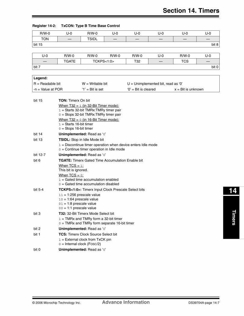
Register 14-2: TxCON: Type B Time Base Control
R/W-0 U-0 R/W-0 U-0 U-0 U-0 U-0 U-0
TON — TSIDL — — — — —
bit 15 bit 8
U-0 R/W-0 R/W-0 R/W-0 R/W-0 U-0 R/W-0 U-0
— TGATE TCKPS<1:0> T32 — TCS —
bit 7 bit 0
Legend:
R = Readable bit W = Writable bit U = Unimplemented bit, read as ‘0’
-n = Value at POR ‘1’ = Bit is set ‘0’ = Bit is cleared x = Bit is unknown
bit 15 TON: Timerx On bitWhen T32 = 1 (in 32-Bit Timer mode):1 = Starts 32-bit TMRx:TMRy timer pair0 = Stops 32-bit TMRx:TMRy timer pairWhen T32 = 0 (in 16-Bit Timer mode):1 = Starts 16-bit timer0 = Stops 16-bit timer
bit 14 Unimplemented: Read as ‘0’
bit 13 TSIDL: Stop in Idle Mode bit1 = Discontinue timer operation when device enters Idle mode0 = Continue timer operation in Idle mode
bit 12-7 Unimplemented: Read as ‘0’
bit 6 TGATE: Timerx Gated Time Accumulation Enable bit
When TCS = 1:This bit is ignored.
When TCS = 0:1 = Gated time accumulation enabled0 = Gated time accumulation disabled
bit 5-4 TCKPS<1:0>: Timerx Input Clock Prescale Select bits11 = 1:256 prescale value10 = 1:64 prescale value01 = 1:8 prescale value00 = 1:1 prescale value
bit 3 T32: 32-Bit Timerx Mode Select bit1 = TMRx and TMRy form a 32-bit timer0 = TMRx and TMRy form separate 16-bit timer
bit 2 Unimplemented: Read as ‘0’
bit 1 TCS: Timerx Clock Source Select bit1 = External clock from TxCK pin0 = Internal clock (FOSC/2)
bit 0 Unimplemented: Read as ‘0’
© 2006 Microchip Technology Inc. Advance Information DS39704A-page 14-7

PIC24F Family Reference Manual
Register 14-3: TyCON: Type C Time Base Control
R/W-0 U-0 R/W-0 U-0 U-0 U-0 U-0 U-0
TON(1) — TSIDL — — — — —
bit 15 bit 8
U-0 R/W-0 R/W-0 R/W-0 U-0 U-0 R/W-0 U-0
— TGATE(1) TCKPS<1:0> — — TCS —
bit 7 bit 0
Legend:
R = Readable bit W = Writable bit U = Unimplemented bit, read as ‘0’
-n = Value at POR ‘1’ = Bit is set ‘0’ = Bit is cleared x = Bit is unknown
bit 15 TON: Timery On bit(1)
1 = Starts 16-bit Timery0 = Stops 16-bit Timery
bit 14 Unimplemented: Read as ‘0’
bit 13 TSIDL: Stop in Idle Mode bit1 = Discontinue timer operation when device enters Idle mode0 = Continue timer operation in Idle mode
bit 12-7 Unimplemented: Read as ‘0’
bit 6 TGATE: Timery Gated Time Accumulation Enable bit(1)
When TCS = 1:This bit is ignored.
When TCS = 0:1 = Gated time accumulation enabled0 = Gated time accumulation disabled
bit 5-4 TCKPS<1:0>: Timery Input Clock Prescale Select bits11 = 1:256 prescale value10 = 1:64 prescale value01 = 1:8 prescale value00 = 1:1 prescale value
bit 3-2 Unimplemented: Read as ‘0’
bit 1 TCS: Timery Clock Source Select bit
1 = External clock from TxCK pin0 = Internal clock (FOSC/2)
bit 0 Unimplemented: Read as ‘0’
Note 1: When 32-bit operation is enabled (T2CON<3> = 1), these bits have no effect on Timery operation; all timer functions are set through T2CON.
DS39704A-page 14-8 Advance Information © 2006 Microchip Technology Inc.

Section 14. TimersTim
ers
14
14.4 MODES OF OPERATION
Each timer module can operate in one of the following modes:• Timer• Synchronous counter
• As a gated timer• Asynchronous counter (Type A and C time base only)
The Timer modes are determined by the following bits:• TCS (TxCON<1>): Timer Clock Source Control bit
• TSYNC (TxCON<2>): Timer Synchronization Control bit (Type A time base only)• TGATE (TxCON<6>): Timer Gate Control bit
Each timer module is enabled or disabled using the TON bit (TxCON <15>).
14.4.1 Timer Mode
All types of timers have the ability to operate in Timer mode based on the system clock. In Timermode, the input clock to the timer is provided from the internal system clock (FOSC/2). Whenenabled, the timer increments once per instruction cycle for a 1:1 prescaler setting. The Timermode is selected by clearing the TCS control bit (TxCON<1>). The Synchronous mode controlbit, TSYNC (TxCON<2>), has no effect, since the system clock source is used to generate thetimer clock.
Example 14-1: Initialization Code for 16-Bit Timer Using System Clock
Note: Only Type A and C time bases support the External Asynchronous Counter mode.
/* The following code example will enable Timer1 interrupts, load the Timer1 Period register and start Timer1.
When a Timer1 period match interrupt occurs, the interrupt service routine must clear the Timer1 interrupt status flag in software.
*/
T1CON = 0x00; //Stops the Timer1 and reset control reg.TMR1 = 0x00; //Clear contents of the timer registerPR1 = 0xFFFF; //Load the Period register with the value 0xFFFFIPC0bits.T1IP = 0x01; //Setup Timer1 interrupt for desired priority level
// (This example assigns level 1 priority)IFS0bits.T1IF = 0; //Clear the Timer1 interrupt status flagIEC0bits.T1IE = 1; //Enable Timer1 interruptsT1CONbits.TON = 1; //Start Timer1 with prescaler settings at 1:1 and
//clock source set to the internal instruction cycle
/* Example code for Timer1 ISR*/
void __attribute__((__interrupt__, __shadow__)) _T1Interrupt(void){
/* Interrupt Service Routine code goes here */
IFS0bits.T1IF = 0; //Reset Timer1 interrupt flag and Return from ISR}
© 2006 Microchip Technology Inc. Advance Information DS39704A-page 14-9
PIC24F Family Reference Manual
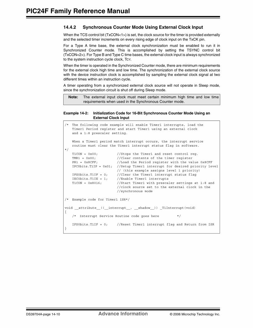
14.4.2 Synchronous Counter Mode Using External Clock Input
When the TCS control bit (TxCON<1>) is set, the clock source for the timer is provided externallyand the selected timer increments on every rising edge of clock input on the TxCK pin.
For a Type A time base, the external clock synchronization must be enabled to run it inSynchronized Counter mode. This is accomplished by setting the TSYNC control bit(TxCON<2>). For Type B and Type C time bases, the external clock input is always synchronizedto the system instruction cycle clock, TCY.
When the timer is operated in the Synchronized Counter mode, there are minimum requirementsfor the external clock high time and low time. The synchronization of the external clock sourcewith the device instruction clock is accomplished by sampling the external clock signal at twodifferent times within an instruction cycle.
A timer operating from a synchronized external clock source will not operate in Sleep mode,since the synchronization circuit is shut off during Sleep mode.
Example 14-2: Initialization Code for 16-Bit Synchronous Counter Mode Using an External Clock Input
Note: The external input clock must meet certain minimum high time and low timerequirements when used in the Synchronous Counter mode.
/* The following code example will enable Timer1 interrupts, load theTimer1 Period register and start Timer1 using an external clockand a 1:8 prescaler setting.
When a Timer1 period match interrupt occurs, the interrupt service routine must clear the Timer1 interrupt status flag in software.
*/T1CON = 0x00; //Stops the Timer1 and reset control reg.TMR1 = 0x00; //Clear contents of the timer registerPR1 = 0x8CFF; //Load the Period register with the value 0x8CFFIPC0bits.T1IP = 0x01; //Setup Timer1 interrupt for desired priority level
// (this example assigns level 1 priority)IFS0bits.T1IF = 0; //Clear the Timer1 interrupt status flagIEC0bits.T1IE = 1; //Enable Timer1 interruptsT1CON = 0x8016; //Start Timer1 with prescaler settings at 1:8 and
//clock source set to the external clock in the //synchronous mode
/* Example code for Timer1 ISR*/
void __attribute__((__interrupt__, __shadow__)) _T1Interrupt(void){
/* Interrupt Service Routine code goes here */
IFS0bits.T1IF = 0; //Reset Timer1 interrupt flag and Return from ISR}
DS39704A-page 14-10 Advance Information © 2006 Microchip Technology Inc.

Section 14. TimersTim
ers
14
14.4.3 Type A Timer Asynchronous Counter Mode Using External Clock Input
A Type A time base has the ability to operate in an Asynchronous Counting mode, using anexternal clock source connected to the TxCK pin. When the TSYNC control bit (TxCON<2>) iscleared, the external clock input is not synchronized with the device system clock source. Thetime base continues to increment asynchronously to the internal device clock.
The asynchronous operation time base is beneficial for the following applications:
• The time base can operate during Sleep mode and can generate an interrupt on period register match that will wake-up the processor.
• The time base can be clocked from the low-power 32 kHz oscillator to provide a secondary system clock source.
Example 14-3: Initialization Code for 16-Bit Asynchronous Counter Mode Using an External Clock Input
Note 1: Only Type A time bases support the Asynchronous Counter mode.
2: The external input clock must meet certain minimum high time and low timerequirements when Timerx is used in the Asynchronous Counter mode.
/* The following code example will enable Timer1 interrupts, load the Timer1 Period register and start Timer1 using an asynchronous external clock and a 1:8 prescaler setting.
When a Timer1 period match interrupt occurs, the interrupt serviceroutine must clear the Timer1 interrupt status flag in software.
*/
T1CON = 0x00; //Stops the Timer1 and reset control reg.TMR1 = 0x00; //Clear contents of the timer registerPR1 = 0x8CFF; //Load the Period register with the value 0x8CFFIPC0bits.T1IP = 0x01; //Setup Timer1 interrupt for desired priority level
// (this example assigns level 1 priority)IFS0bits.T1IF = 0; //Clear the Timer1 interrupt status flagIEC0bits.T1IE = 1; //Enable Timer1 interruptsT1CON = 0x8012; //Start Timer1 with prescaler settings at 1:8 and
//clock source set to the external clock in the //asynchronous mode
/* Example code for Timer1 ISR*/
void __attribute__((__interrupt__, __shadow__)) _T1Interrupt(void){
/* Interrupt Service Routine code goes here */
IFS0bits.T1IF = 0; //Reset Timer1 interrupt flag and Return from ISR}
© 2006 Microchip Technology Inc. Advance Information DS39704A-page 14-11

PIC24F Family Reference Manual
14.4.4 Timer Operation with Fast External Clock Source
In some applications, it may be desirable to use one of the timers to count clock edges from arelatively high-frequency external clock source. In these situations, Type A and Type B timebases are the most suitable choices for counting the external clock source because the clocksynchronization logic for these timers is located after the timer prescaler (see Figure 14-1 andFigure 14-2). This allows a higher external clock frequency to be used that will not violate theminimum high and low times required by the prescaler. When a timer prescaler ratio other than1:1 is selected for a Type A or Type B time base, the minimum high and low times for the externalclock input are reduced by the chosen prescaler ratio.
A Type A time base is unique because it can be operated in an Asynchronous mode, eliminatingany prescaler timing requirements.
Note that in all cases, there are minimum high and low times for the external clock signal thatcannot be exceeded. These minimum times are required to satisfy the I/O pin timingrequirements.
Please refer to the specific device data sheet for the external clock timing specifications associatedwith the time bases.
14.4.5 Gated Time Accumulation Mode
The Gated Time Accumulation mode allows the internal timer register to increment based uponthe duration of the high time applied to the TxCK pin. In the Gated Time Accumulation mode, thetimer clock source is derived from the internal system clock. When the TxCK pin state is high, thetimer register will count up until a period match has occurred, or the TxCK pin state is changedto a low state. A pin state transition from high-to-low will set the TxIF interrupt flag. Dependingon when the edge occurs, the interrupt flag is asserted 1 or 2 instruction cycles after the fallingedge of the signal on the TxCK pin.
The TGATE control bit (TxCON<6>) must be set to enable the Gated Time Accumulation mode.The timer must be enabled, TON (TxCON<15>) = 1, and the timer clock source set to the internalclock, TCS (TxCON<1>) = 0.
The gate operation starts on a rising edge of the signal applied to the TxCK pin and terminateson the falling edge of the signal applied to the TxCK pin. The respective timer will increment whilethe external gate signal is high.
The falling edge of the gate signal sets the TxIF interrupt flag and generates an interrupt ifenabled.
The resolution of the timer count is directly related to the timer clock period. For a timer prescalerof 1:1, the timer clock period is one instruction cycle. For a timer prescaler of 1:256, the timerclock period is 256 times the instruction cycle. The timer clock resolution can be associated withthe pulse width of the gate signal. Refer to the “Electrical Characteristics” section in thespecific device data sheet for further details on the gate width pulse requirements.
Note: The timer will not interrupt the CPU when a timer period match occurs in Gate TimeAccumulation mode.
DS39704A-page 14-12 Advance Information © 2006 Microchip Technology Inc.

Section 14. TimersTim
ers
14
Figure 14-4: Gated Timer Mode Operation
Example 14-4: Initialization Code for 16-Bit Gated Time Accumulation Mode
/* The following code example will enable Timer2 interrupts, load the Timer2 Period register and start Timer2 using an internal clock and an external gate signal. On the falling edge of the gate signal a Timer2 interrupt occurs. The interrupt service routine must clear the Timer2 interrupt status flag in software .
*/T2CON = 0x00; //Stops the Timer2 and reset control reg.TMR2 = 0x00; //Clear contents of the timer registerPR2 = 0xFFFF; //Load the Period register with the value 0xFFFFIPC1bits.T2IP = 0x01; //Setup Timer2 interrupt for desired priority level
// (this example assigns level 1 priority)IFS0bits.T2IF = 0; //Clear the Timer2 interrupt status flagIEC0bits.T2IE = 1; //Enable Timer2 interruptsT2CONbits.TGATE = 1; //Set up Timer2 for operation in Gated
//Time Accumulation modeT2CONbits.TON = 1; //Start Timer2
void __attribute__((__interrupt__, __shadow__)) _T2Interrupt(void){
/* Interrupt Service Routine code goes here */
IFS0bits.T2IF = 0; //Reset Timer2 interrupt flag and Return from ISR}
TxIF
0001 0002TMRx
1 Instruction Cycle (TCY)
00040003
TxCK pin
0005
TxIF bit cleared by user in software.
0000
© 2006 Microchip Technology Inc. Advance Information DS39704A-page 14-13

PIC24F Family Reference Manual
14.5 TIMER PRESCALERS
The input clock (FOSC/2 or external clock) to all 16-bit timers has prescale options of 1:1, 1:8,1:64 and 1:256. The clock prescaler is selected using the TCKPS<1:0> control bits(TxCON<5:4>). The prescaler counter is cleared when any of the following occurs:
• A write to the TMRx register• Clearing TON (TxCON<15>) to ‘0’
• Any device Reset
14.6 TIMER INTERRUPTS
A 16-bit timer has the ability to generate an interrupt on a period match or falling edge of theexternal gate signal, depending on the operating mode.
The TxIF bit is set when one of the following conditions is true:
• The timer count matches the respective period register and the timer module is not operating in Gated Time Accumulation mode.
• The falling edge of the “gate” signal is detected when the timer is operating in Gated Time Accumulation mode.
The TxIF bit must be cleared in software.
A timer is enabled as a source of interrupt via the respective Timer Interrupt Enable bit, TxIE.Furthermore, the interrupt priority level bits (TxIP<2:0>) must be written with a non-zero value inorder for the timer to be a source of interrupt. Refer to Section 8. “Interrupts” for further details.
Figure 14-5: Interrupt Timing for Timer Period Match
Note: The TMRx register is not cleared when TxCON is written.
Note: A special case occurs when the period register, PRx, is loaded with 0x0000 and thetimer is enabled. No timer interrupts will be generated for this configuration.
TxIF
0003 000547FE 47FF 4800 000047FDTMR2 0004
1 Instruction Cycle (TCY)
4800PR2
00020001
Cleared by User
TMR2 Resets Here
DS39704A-page 14-14 Advance Information © 2006 Microchip Technology Inc.

Section 14. TimersTim
ers
14
14.7 READING AND WRITING 16-BIT TIMER MODULE REGISTERS
• All timer module SFRs can be written to as a byte (8 bits) or as a word (16 bits).• All timer module SFRs can only be read as a word (16 bits).
14.7.1 Writing to the 16-Bit Timers
The timer and its respective period register can be written to while the module is operating. Theuser should be aware of the following when byte writes are performed:
• If the timer is incrementing and the low byte of the timer is written to, the upper byte of the timer is not affected. If 0xFF is written into the low byte of the timer, the next timer count clock after this write will cause the low byte to rollover to 0x00 and generate a carry into the high byte of the timer.
• If the timer is incrementing and the high byte of the timer is written to, the low byte of the timer is not affected. If the low byte of the timer contains 0xFF when the write occurs, the next timer count clock will generate a carry from the timer low byte and this carry will cause the upper byte of the timer to increment.
When the TMRx register is written to (word or byte) via an instruction, the TMRx registerincrement is masked and does not occur during that instruction cycle.
Writes to a timer with an Asynchronous mode should be avoided in a real timekeeping application.See Section 14.4.1 “Timer Mode” for information on Asynchronous Counter mode.
14.7.2 Reading From the 16-Bit Timers
All reads of the timers and their associated SFRs must be word reads (16 bits). A byte read willhave no effect (‘0’ will be returned).
The timer and respective period register can be read while the module is operating. A read of theTMRx register does not prevent the timer from incrementing during the same instruction cycle.
14.8 SECONDARY OSCILLATOR 32 kHz CRYSTAL INPUT
In each device variant, a 32 kHz crystal oscillator is available to the Type A timer module forReal-Time Clock (RTC) type of applications.
• The secondary oscillator becomes the clock source for the timer when the secondary oscillator is enabled and the timer is configured to use the external clock source.
• The secondary oscillator is enabled by setting the SOSCEN control bit in the OSCCON register.
• The 32 kHz crystal is connected to the SOSCO/SOSCI device pins.
Refer to Section 6. “Oscillator” for further details.
© 2006 Microchip Technology Inc. Advance Information DS39704A-page 14-15

PIC24F Family Reference Manual
14.9 32-BIT TIMER CONFIGURATION
A 32-bit timer module can be formed by combining a Type B and a Type C 16-bit timer module.The Type C time base becomes the most significant word (msw) of the combined timer and theType B time base is the least significant word (lsw).
When configured for 32-bit operation, the control bits for the Type B time base control the operationof the 32-bit timer. The control bits in the TxCON register for the Type C time base have no effect.
For interrupt control, the combined 32-bit timer uses the interrupt enable, interrupt flag andinterrupt priority control bits of the Type C time base. The interrupt control and status bits for theType B time base are not used during 32-bit timer operation.
The following configuration settings assume Timer3 is a Type C time base and Timer2 is a Type Btime base:
• TON (T2CON<15>) = 1.• T32 (T2CON<3>) = 1.• TCKPS<1:0> bits (T2CON<5:4>) are used to set the Prescaler mode for Timer2
(Type B time base).• The TMR3:TMR2 register pair contains the 32-bit value of the timer module. The TMR3
(Type C time base) register is the most significant word, while the TMR2 (Type B time base) register is the least significant word of the 32-bit timer value.
• The PR3:PR2 register pair contains the 32-bit period value that is used for comparison with the TMR3:TMR2 timer value.
• T3IE (IEC0<8>) is used to enable the 32-bit timer interrupt for this configuration.• T3IF (IFS0<8>) is used as a status flag for the timer interrupt.
• T3IP<2:0> bits (IPC2<2:0>) set the interrupt priority level for the 32-bit timer.• T3CON<15:0> are “don’t care” bits.
A block diagram representation of the 32-bit timer module using Timer2 and Timer3 as anexample is shown in Figure 14-6.
Note: Refer to the specific device data sheet for information on the Type B and Type Ctime bases that can be combined.
Note: Input capture and output compare are not available in 32-Bit Timer mode.
DS39704A-page 14-16 Advance Information © 2006 Microchip Technology Inc.

Section 14. TimersTim
ers
14
Figure 14-6: Type B/Type C Timer Pair Block Diagram (32-Bit Timer)
TMR3 TMR2
Set T3IF (T5IF)
EqualComparator
PR3 PR2
Reset
LSB MSB
Note: The 32-bit Timer Configuration bit, T32, must be set for 32-bit timer/counter operation. All control bits arerespective to the T2CON and T4CON registers.
Data Bus<15:0>
TMR3HLD
Read TMR2 (TMR4)
Write TMR2 (TMR4)16
16
16
Q
Q D
CK
TGATE
0
1
TON
TCKPS1:TCKPS0
Prescaler1, 8, 64, 256
2
TCY
TCS
1x
01
TGATE
00
Gate
T2CK
Sync
ADC Event Trigger*
Sync
(T4CK)
(PR5) (PR4)
(TMR5HLD)
(TMR5) (TMR4)
* The ADC Event Trigger is available only on Timer4/5.
© 2006 Microchip Technology Inc. Advance Information DS39704A-page 14-17

PIC24F Family Reference Manual
14.10 32-BIT TIMER MODES OF OPERATION
14.10.1 Timer Mode
Example 14-5 shows how to configure a 32-bit timer in Timer mode. This example assumesTimer2 is a Type B time base and Timer3 is a Type C time base. For 32-bit timer operation, theT32 control bit must be set in the T2CON register (Type B time base). When Timer2 and Timer3are configured for a 32-bit timer, the T3CON control bits are ignored. Only the T2CON controlbits are required for setup and control. The Timer2 clock and gate input is utilized for the 32-bittimer module, but an interrupt is generated with the T3IF flag. Timer2 is the lsw and Timer3 is themsw of the 32-bit timer. TMR3 is incremented by an overflow (carry out) from TMR2. The 32-bittimer increments up to a match value preloaded into the combined 32-bit period register, formedby PR2 and PR3, then rolls over and continues. For a maximum 32-bit timer count, loadPR3:PR2 with a value of 0xFFFFFFFF. An interrupt is generated on a period match if enabled.
Example 14-5: Initialization Code for 32-Bit Timer Using Instruction Cycle as Input Clock
/* The following code example will enable Timer3 interrupts, load the Timer3:Timer2 Period Register and start the 32-bit timer module consisting of Timer3 and Timer2.
When a 32-bit period match interrupt occurs, the user must clear the Timer3 interrupt status flag in software.
*/T2CON = 0x00; //Stops any 16/32-bit Timer2 operationT3CON = 0x00; //Stops any 16-bit Timer3 operationTMR3 = 0x00; //Clear contents of the timer3 registerTMR2 = 0x00; //Clear contents of the timer2 registerPR3 = 0xFFFF; //Load the Period register3 with the value 0xFFFFPR2 = 0xFFFF; //Load the Period register2 with the value 0xFFFF
IPC2bits.T3IP = 0x01; //Setup Timer3 interrupt for desired priority level//(this example assigns level 1 priority)
IFS0bits.T3IF = 0; //Clear the Timer3 interrupt status flagIEC0bits.T3IE = 1; //Enable Timer3 interruptsT2CONbits.T32 = 1; //Enable 32-bit Timer operationT2CONbits.TON = 1; //Start 32-bit timer with prescaler
//settings at 1:1 and clock source set to//the internal instruction cycle
void __attribute__((__interrupt__, __shadow__)) _T3Interrupt(void){
/* Interrupt Service Routine code goes here */
IFS0bits.T3IF = 0; //Reset Timer1 interrupt flag and Return from ISR}
DS39704A-page 14-18 Advance Information © 2006 Microchip Technology Inc.

Section 14. TimersTim
ers
14
14.10.2 Synchronous Counter Mode
The 32-bit timer operates similarly to a 16-bit timer in Synchronous Counter mode. Example 14-6shows how to configure a 32-bit timer in Synchronous Counter mode. This example assumesTimer2 is a Type B time base and Timer3 is a Type C time base.
Example 14-6: Initialization Code for 32-Bit Synchronous Counter Mode Using an External Clock Input
/* The following code example will enable Timer2 interrupts, load the Timer3:Timer2 Period register and start the 32-bit timer module consisting of Timer3 and Timer2.
When a 32-bit period match interrupt occurs, the user must clear the Timer3 interrupt status flag in the software.
*/T2CON = 0x00; //Stops any 16/32-bit Timer2 operationT3CON = 0x00; //Stops any 16-bit Timer3 operationTMR3 = 0x00; //Clear contents of the timer3 registerTMR2 = 0x00; //Clear contents of the timer2 registerPR3 = 0xFFFF; //Load the Period register3 with the value 0xFFFFPR2 = 0xFFFF; //Load the Period register2 with the value 0xFFFF
IPC2bits.T3IP = 0x01; //Setup Timer3 interrupt for desired priority level//(this example assigns level 1 priority)
IFS0bits.T3IF = 0; //Clear the Timer3 interrupt status flagIEC0bits.T3IE = 1; //Enable Timer3 interruptsT2CON = 0x801A; //Enable 32-bit Timer operation and start
//32-bit timer with prescaler settings at 1:8 //and clock source set to external clock
void __attribute__((__interrupt__, __shadow__)) _T3Interrupt(void){
/* Interrupt Service Routine code goes here */
IFS0bits.T3IF = 0; //Reset Timer1 interrupt flag and Return from ISR}
© 2006 Microchip Technology Inc. Advance Information DS39704A-page 14-19
PIC24F Family Reference Manual
14.10.3 Asynchronous Counter Mode
Type B and Type C time bases do not support the Asynchronous External Clock mode, therefore,no 32-bit Asynchronous Counter mode is supported.
14.10.4 Gated Time Accumulation Mode
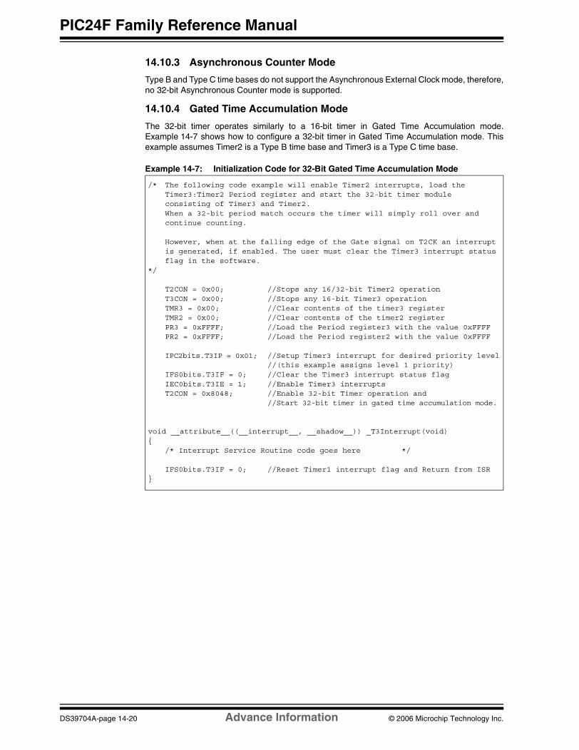
The 32-bit timer operates similarly to a 16-bit timer in Gated Time Accumulation mode.Example 14-7 shows how to configure a 32-bit timer in Gated Time Accumulation mode. Thisexample assumes Timer2 is a Type B time base and Timer3 is a Type C time base.
Example 14-7: Initialization Code for 32-Bit Gated Time Accumulation Mode /* The following code example will enable Timer2 interrupts, load the
Timer3:Timer2 Period register and start the 32-bit timer module consisting of Timer3 and Timer2. When a 32-bit period match occurs the timer will simply roll over and continue counting.
However, when at the falling edge of the Gate signal on T2CK an interrupt is generated, if enabled. The user must clear the Timer3 interrupt status flag in the software.
*/
T2CON = 0x00; //Stops any 16/32-bit Timer2 operationT3CON = 0x00; //Stops any 16-bit Timer3 operationTMR3 = 0x00; //Clear contents of the timer3 registerTMR2 = 0x00; //Clear contents of the timer2 registerPR3 = 0xFFFF; //Load the Period register3 with the value 0xFFFFPR2 = 0xFFFF; //Load the Period register2 with the value 0xFFFF
IPC2bits.T3IP = 0x01; //Setup Timer3 interrupt for desired priority level//(this example assigns level 1 priority)
IFS0bits.T3IF = 0; //Clear the Timer3 interrupt status flagIEC0bits.T3IE = 1; //Enable Timer3 interruptsT2CON = 0x8048; //Enable 32-bit Timer operation and
//Start 32-bit timer in gated time accumulation mode.
void __attribute__((__interrupt__, __shadow__)) _T3Interrupt(void){
/* Interrupt Service Routine code goes here */
IFS0bits.T3IF = 0; //Reset Timer1 interrupt flag and Return from ISR}
DS39704A-page 14-20 Advance Information © 2006 Microchip Technology Inc.

Section 14. TimersTim
ers
14
14.11 READING AND WRITING INTO 32-BIT TIMERS
In order for 32-bit read/write operations to be synchronized between the lsw and msw of the32-bit timer, additional control logic and holding registers are utilized (see Figure 14-6). EachType C time base has a register called TMRxHLD that is used when reading or writing the timerregister pair. The TMRxHLD registers are only used when their respective timers are configuredfor 32-bit operation.
Assuming TMR3:TMR2 form a 32-bit timer pair, the user should first read the lsw of the timervalue from the TMR2 register. The read of the lsw will automatically transfer the contents ofTMR3 into the TMR3HLD register. The user can then read TMR3HLD to get the msw of the timervalue. This is shown in Example 14-8:
Example 14-8: Reading From a 32-Bit Timer
To write a value to the TMR3:TMR2 register pair, the user should first write the msw to theTMR3HLD register. When the lsw of the timer value is written to TMR2, the contents ofTMR3HLD will automatically be transferred to the TMR3 register.
14.12 TIMER OPERATION IN POWER-SAVING STATES
14.12.1 Timer Operation in Sleep Mode
When the device enters Sleep mode, the system clock is disabled. If the timer module is runningfrom the internal clock source (FOSC/2), it will also be disabled.
A Type A timer is different from the other timer modules because it can operate asynchronouslyfrom the system clock source. Because of this distinction, the Type A time base module cancontinue to operate during Sleep mode. To operate in Sleep mode, the Type A time base mustbe configured as follows:
• The Timer1 module is enabled, TON (TxCON<15>) = 1;
• The Timer1 clock source is selected as external, TCS (TxCON<1>) = 1 and• The TSYNC bit (TxCON<2>) is set to logic ‘0’ (Asynchronous Counter mode enabled).
When all of the above conditions are met, Timer1 will continue to count and detect periodmatches when the device is in Sleep mode. When a match between the timer and the periodregister occurs, the TxIF bit will be set and an interrupt can be generated to optionally wake thedevice from Sleep. Refer to Section 10. “Power-Saving Features” for further details.
14.12.2 Timer Operation in Idle Mode
When the device enters Idle mode, the system clock sources remain functional and the CPUstops executing code. The timer modules can optionally continue to operate in Idle mode.
The TSIDL bit (TxCON<13>) selects if the timer module will stop in Idle mode or continue tooperate normally. If TSIDL = 0, the module will continue operation in Idle mode. If TSIDL = 1, themodule will stop in Idle mode.
14.12.3 Timer Operation in Doze Mode
Timer operation in Doze mode is the same as in normal mode. When the device enters Dozemode, the system clock sources remain functional and the CPU may run at a slower clock rate.Refer to Section 10. “Power-Saving Features” for further details.
/* The following code segment reads the 32-bit timer formed by theTimer3-Timer2 pair into the registers W1(MS Word) and W0(LS Word).
*/unsigned int temp_lsb;unsigned int temp_msb;
temp_lsb = TMR2; //Transfer the LSW into temp_lsbtemp_msb = TMR3HLD; //Transfer the MSW from the holding register to into
//temp_msb
Note: Asynchronous counter operation is only supported for the Timer1 module.
© 2006 Microchip Technology Inc. Advance Information DS39704A-page 14-21

PIC24F Family Reference Manual
14.13 PERIPHERALS USING TIMER MODULES
14.13.1 Time Base for Input Capture/Output Compare
The input capture and output compare peripherals can select one of two timer modules as theirtime base. Refer to Section 15. “Input Capture”, Section 16. “Output Compare” and thespecific device data sheet for further details.
14.13.2 A/D Special Event Trigger
On each device variant, one Type C time base has the capability to generate a special A/Dconversion trigger signal, on a period match, in both 16 and 32-bit modes. The timer moduleprovides a conversion start signal to the A/D sampling logic.
• If T32 = 0 when a match occurs between the 16-bit timer register (TMRx) and the respective 16-bit period register (PRx), the A/D Special Event Trigger signal is generated.
• If T32 = 1 when a match occurs between the 32-bit timer (TMRx:TMRy) and the 32-bit respective combined period register (PRx:PRy), the A/D Special Event Trigger signal is generated.
The Special Event Trigger signal is always generated by the timer. The trigger source must beselected in the A/D converter control registers. Refer to Section 17. “10-Bit A/D Converter” andthe specific device data sheet for additional information.
14.13.3 Timer as an External Interrupt Pin
The external clock input pin for each timer can be used as an additional interrupt pin. To providethe interrupt, the timer period register, PRx, is written with a non-zero value and the TMRxregister is initialized to a value of 1 less than the value written to the period register. The timermust be configured for a 1:1 clock prescaler. An interrupt will be generated when the next risingedge of the external clock signal is detected.
14.13.4 I/O Pin Control
When a timer module is enabled and configured for external clock or gate operation, the usermust ensure the I/O pin direction is configured for an input. Enabling the timer module does notconfigure the pin direction.
14.13.5 Enabling Timer
To enable the timer, the Timer Module Disable bit (TxMD in PMD1 register) must be cleared alongwith setting the module enable bit. Setting the TxMD bit will disable all clock sources to thatmodule, reducing its power consumption to an absolute minimum. In this state, the control andstatus registers associated with the peripheral will also be disabled, so writes to those registerswill have no effect and read values will be invalid.
DS39704A-page 14-22 Advance Information © 2006 Microchip Technology Inc.

Section 14. TimersT
imers
14
14.1
4 R
EG
IST
ER
MA
PS
A s
umm
ary
of th
e S
peci
al F
unct
ion
Reg
iste
rs a
ssoc
iate
d w
ith th
e P
IC24
F ti
mer
mod
ule
is p
rovi
ded
in T
able
14-1
.
Tab
le 1
4-1:
Sp
ecia
l Fu
nct
ion
Reg
iste
rs A
sso
ciat
ed w
ith
Tim
er M
od
ule
s
SF
RN
ame
Bit
15
Bit
14
Bit
13
Bit
12
Bit
11
Bit
10
Bit
9B
it 8
Bit
7B
it 6
Bit
5B
it 4
Bit
3B
it 2
Bit
1B
it 0
All
Res
ets
PM
D1
T5M
DT
4MD
T3M
DT
2MD
T1M
D—
——
I2C
1MD
U2M
DU
1MD
SP
I2M
DS
PI1
MD
——
AD
CM
D0000
TM
R1
Tim
er1
Reg
iste
rxxxx
PR
1P
erio
d R
egis
ter
1FFFF
T1C
ON
TO
N—
TS
IDL
——
——
——
TG
AT
ET
CK
PS
1T
CK
PS
0—
TS
YN
CT
CS
—0000
TM
R2
Tim
er2
Reg
iste
rxxxx
TM
R3H
LDTi
mer
3 H
oldi
ng R
egis
ter
(for
32-
bit t
imer
ope
ratio
ns o
nly)
xxxx
TM
R3
Tim
er3
Reg
iste
rxxxx
PR
2P
erio
d R
egis
ter
2FFFF
PR
3P
erio
d R
egis
ter
3FFFF
T2C
ON
TO
N—
TS
IDL
——
——
——
TG
AT
ET
CK
PS
1T
CK
PS
0T
32—
TC
S—
0000
T3C
ON
TO
N—
TS
IDL
——
——
——
TG
AT
ET
CK
PS
1T
CK
PS
0—
—T
CS
—0000
TM
R4
Tim
er4
Reg
iste
rxxxx
TM
R5H
LDTi
mer
5 H
oldi
ng R
egis
ter
(for
32-
bit t
imer
ope
ratio
ns o
nly)
xxxx
TM
R5
Tim
er5
Reg
iste
rxxxx
PR
4P
erio
d R
egis
ter
4FFFF
PR
5P
erio
d R
egis
ter
5FFFF
T4C
ON
TO
N—
TS
IDL
——
——
——
TG
AT
ET
CK
PS
1T
CK
PS
0T
32—
TC
S—
0000
T5C
ON
TO
N—
TS
IDL
——
——
——
TG
AT
ET
CK
PS
1T
CK
PS
0—
—T
CS
—0000
IFS
0—
—A
D1I
FU
1TX
IFU
1RX
IFS
PI1
IFS
PF
1IF
T3I
FT
2IF
OC
2IF
IC2I
F—
T1I
FO
C1I
FIC
1IF
INT
01F
0000
IFS
1U
2TX
IFU
2RX
IFIN
T2I
FT
5IF
T4I
FO
C4I
FO
C3I
F—
——
—IN
T1I
FC
NIF
CM
IFM
2C1I
FS
I2C
1IF
0000
IEC
0—
—A
D1I
EU
1TX
IEU
1RX
IES
PI1
IES
PF
1IE
T3I
ET
2IE
OC
2IE
IC2I
E—
T1I
EO
C1I
EIC
1IE
INT
01E
0000
IEC
1U
2TX
IEU
2RX
IEIN
T2I
ET
5IE
T4I
EO
C4I
EO
C3I
E—
——
—IN
T1I
EC
NIE
CM
IEM
2C1I
ES
I2C
1IE
0000
IPC
0—
T1I
P2
T1I
P1
T1I
P0
—O
C1I
P2
OC
1IP
1O
C1I
P0
—IC
1IP
2IC
1IP
1IC
1IP
0—
INT
0IP
2IN
T0I
P1
INT
0IP
04444
IPC
1—
T2I
P2
T2I
P1
T2I
P0
—O
C2I
P2
OC
2IP
1O
C2I
P0
—IC
2IP
2IC
2IP
1IC
2IP
0—
——
—4440
IPC
2—
U1R
XIP
2U
1RX
IP1
U1R
XIP
0—
SP
I1IP
2S
PI1
IP1
SP
I1IP
0—
SP
F1I
P2
SP
F1I
P1
SP
F1I
P0
—T
3IP
2T
3IP
1T
3IP
04444
IPC
6—
T4I
P2
T4I
P1
T4I
P0
—O
C4I
P2
OC
4IP
1O
C4I
P0
—O
C3I
P2
OC
3IP
1O
C3I
P0
——
——
4440
IPC
7—
U2T
XIP
2U
2TX
IP1
U2T
XIP
0—
U2R
XIP
2U
2RX
IP1
U2R
XIP
0—
INT
2IP
2IN
T2I
P1
INT
2IP
0—
T5I
P2
T5I
P1
T5I
P0
4444
No
te:
Ple
ase
refe
r to
the
spec
ific
devi
ce d
ata
shee
t for
mem
ory
map
det
ails
.
© 2006 Microchip Technology Inc. Advance Information DS39704A-page 14-23

PIC24F Family Reference Manual
14.15 RELATED APPLICATION NOTES
This section lists application notes that are related to this section of the manual. Theseapplication notes may not be written specifically for the PIC24F device family, but the conceptsare pertinent and could be used with modification and possible limitations. The currentapplication notes related to the Timer modules are:
Title Application Note #
Using Timer1 in Asynchronous Clock Mode AN580
Note: Please visit the Microchip web site (www.microchip.com) for additional applicationnotes and code examples for the PIC24F family of devices.
DS39704A-page 14-24 Advance Information © 2006 Microchip Technology Inc.

Section 14. TimersTim
ers
14
14.16 REVISION HISTORY
Revision A (April 2006)This is the initial released revision of this document.
© 2006 Microchip Technology Inc. Advance Information DS39704A-page 14-25

PIC24F Family Reference Manual
NOTES:
DS39704A-page 14-26 Advance Information © 2006 Microchip Technology Inc.