Embed Size (px)
Citation preview

ADCS FOR DSP APPLICATIONS
3.a
SECTION 3
ADCs FOR DSP APPLICATIONS
Successive Approximation ADCs
Sigma-Delta ADCs
Flash Converters
Subranging (Pipelined) ADCs
Bit-Per-Stage (Serial, or Ripple) ADCs

ADCS FOR DSP APPLICATIONS
3.b

ADCS FOR DSP APPLICATIONS
3.1
SECTION 3
ADCs FOR DSP APPLICATIONSWalt Kester, James BryantThe trend in ADCs and DACs is toward higher speeds and higher resolutions atreduced power levels and supply voltages. Modern data converters generally operateon ±5V (dual supply), +5V or +3V (single supply). In fact, the number of +3V devicesis rapidly increasing because of many new markets such as digital cameras,camcorders, and cellular telephones. This trend has created a number of design andapplications problems which were much less important in earlier data converters,where ±15V supplies and ±10V input ranges were the standard.
Lower supply voltages imply smaller input voltage ranges, and hence moresusceptibility to noise from all potential sources: power supplies, references, digitalsignals, EMI/RFI, and probably most important, improper layout, grounding, anddecoupling techniques. Single-supply ADCs often have an input range which is notreferenced to ground. Finding compatible single-supply drive amplifiers and dealingwith level shifting of the input signal in direct-coupled applications also becomes achallenge.
In spite of these issues, components are now available which allow extremely highresolutions at low supply voltages and low power. This section discusses theapplications problems associated with such components and shows techniques forsuccessfully designing them into systems.
The most popular ADCs for DSP applications are based on five fundamentalarchitectures: successive approximation, sigma-delta, flash, subranging (orpipelined), and bit-per-stage (or ripple).
Figure 3.1
LOW POWER, LOW VOLTAGE ADC DESIGN ISSUES
Typical Supply Voltages: ±5V, +5V, +5/+3V, +3V
Lower Signal Swings Increase Sensitivity to
All Types of Noise (Device, Power Supply, Logic, etc.)
Device Noise Increases at Low Currents
Common Mode Input Voltage Restrictions
Input Buffer Amplifier Selection Critical
Auto-Calibration Modes Desirable at High Resolutions

ADCS FOR DSP APPLICATIONS
3.2
Figure 3.2
SUCCESSIVE APPROXIMATION ADCS
The successive approximation ADC has been the mainstay of signal conditioning formany years. Recent design improvements have extended the sampling frequency ofthese ADCs into the megahertz region. The use of internal switched capacitortechniques along with auto calibration techniques extend the resolution of theseADCs to 16-bits on standard CMOS processes without the need for expensive thin-film laser trimming.
The basic successive approximation ADC is shown in Figure 3.3. It performsconversions on command. On the assertion of the CONVERT START command, thesample-and-hold (SHA) is placed in the hold mode, and all the bits of the successiveapproximation register (SAR) are reset to "0" except the MSB which is set to "1".The SAR output drives the internal DAC. If the DAC output is greater than theanalog input, this bit in the SAR is reset, otherwise it is left set. The next mostsignificant bit is then set to "1". If the DAC output is greater than the analog input,this bit in the SAR is reset, otherwise it is left set. The process is repeated with eachbit in turn. When all the bits have been set, tested, and reset or not as appropriate,the contents of the SAR correspond to the value of the analog input, and theconversion is complete. These bit “tests” can form the basis of a serial outputversion SAR-based ADC.
ADCs FOR DSP APPLICATIONS
Successive Approximation Resolutions to 16-bits Minimal Throughput Delay Time (No Output Latency,
"Single-Shot" Operation Possible Used in Multiplexed Data Acquisition Systems
Sigma-Delta Resolutions to 24-bits Excellent Differential Linearity Internal Digital Filter (Can be Linear Phase) Long Throughput Delay Time (Output Latency) Difficult to Multiplex Inputs Due to Digital Filter Settling Time
High Speed Architectures: Flash Converter Subranging or Pipelined Bit-Per-Stage (Ripple)

ADCS FOR DSP APPLICATIONS
3.3
The end of conversion is generally indicated by an end-of-convert (EOC), data-ready(DRDY), or a busy signal (actually, not-BUSY indicates end of conversion). Thepolarities and name of this signal may be different for different SAR ADCs, but thefundamental concept is the same. At the beginning of the conversion interval, thesignal goes high (or low) and remains in that state until the conversion iscompleted, at which time it goes low (or high). The trailing edge is generally anindication of valid output data.
Figure 3.3
An N-bit conversion takes N steps. It would seem on superficial examination that a16-bit converter would have twice the conversion time of an 8-bit one, but this is notthe case. In an 8-bit converter, the DAC must settle to 8-bit accuracy before the bitdecision is made, whereas in a 16-bit converter, it must settle to 16-bit accuracy,which takes a lot longer. In practice, 8-bit successive approximation ADCs canconvert in a few hundred nanoseconds, while 16-bit ones will generally take severalmicroseconds.
Notice that the overall accuracy and linearity of the SAR ADC is determinedprimarily by the internal DAC. Until recently, most precision SAR ADCs used laser-trimmed thin-film DACs to achieve the desired accuracy and linearity. The thin-filmresistor trimming process adds cost, and the thin-film resistor values may beaffected when subjected to the mechanical stresses of packaging.
For these reasons, switched capacitor (or charge-redistribution) DACs have becomepopular in newer SAR ADCs. The advantage of the switched capacitor DAC is thatthe accuracy and linearity is primarily determined by photolithography, which inturn controls the capacitor plate area and the capacitance as well as matching. In
SUCCESSIVE APPROXIMATION ADC
SHA
SUCCESSIVEAPPROXIMATION
REGISTER(SAR)
DAC
TIMING
CONVERTSTART
EOC,DRDY,
OR BUSY
OUTPUT
ANALOGINPUT COMPARATOR

ADCS FOR DSP APPLICATIONS
3.4
addition, small capacitors can be placed in parallel with the main capacitors whichcan be switched in and out under control of autocalibration routines to achieve highaccuracy and linearity without the need for thin-film laser trimming. Temperaturetracking between the switched capacitors can be better than 1ppm/ºC, therebyoffering a high degree of temperature stability.
A simple 3-bit capacitor DAC is shown in Figure 3.4. The switches are shown in thetrack, or sample mode where the analog input voltage, AIN, is constantly chargingand discharging the parallel combination of all the capacitors. The hold mode isinitiated by opening SIN, leaving the sampled analog input voltage on the capacitorarray. Switch SC is then opened allowing the voltage at node A to move as the bitswitches are manipulated. If S1, S2, S3, and S4 are all connected to ground, avoltage equal to –AIN appears at node A. Connecting S1 to VREF adds a voltageequal to VREF/2 to –AIN. The comparator then makes the MSB bit decision, andthe SAR either leaves S1 connected to VREF or connects it to ground depending onthe comparator output (which is high or low depending on whether the voltage atnode A is negative or positive, respectively). A similar process is followed for theremaining two bits. At the end of the conversion interval, S1, S2, S3, S4, and SINare connected to AIN, SC is connected to ground, and the converter is ready foranother cycle.
Figure 3.4
Note that the extra LSB capacitor (C/4 in the case of the 3-bit DAC) is required tomake the total value of the capacitor array equal to 2C so that binary division isaccomplished when the individual bit capacitors are manipulated.
3-BIT SWITCHED CAPACITOR DAC
_
+C/ 4C/ 2C C/ 4
AIN
VREF
SIN
SC
S1 S2 S3 S4
BIT1(MSB)
BIT2 BIT3(LSB)
SWITCHES SHOWN IN TRACK (SAMPLE) MODE
A
CTOTAL = 2C
ADCS FOR DSP APPLICATIONS
3.5
The operation of the capacitor DAC (cap DAC) is similar to an R/2R resistive DAC.When a particular bit capacitor is switched to VREF, the voltage divider created bythe bit capacitor and the total array capacitance (2C) adds a voltage to node A equalto the weight of that bit. When the bit capacitor is switched to ground, the samevoltage is subtracted from node A.
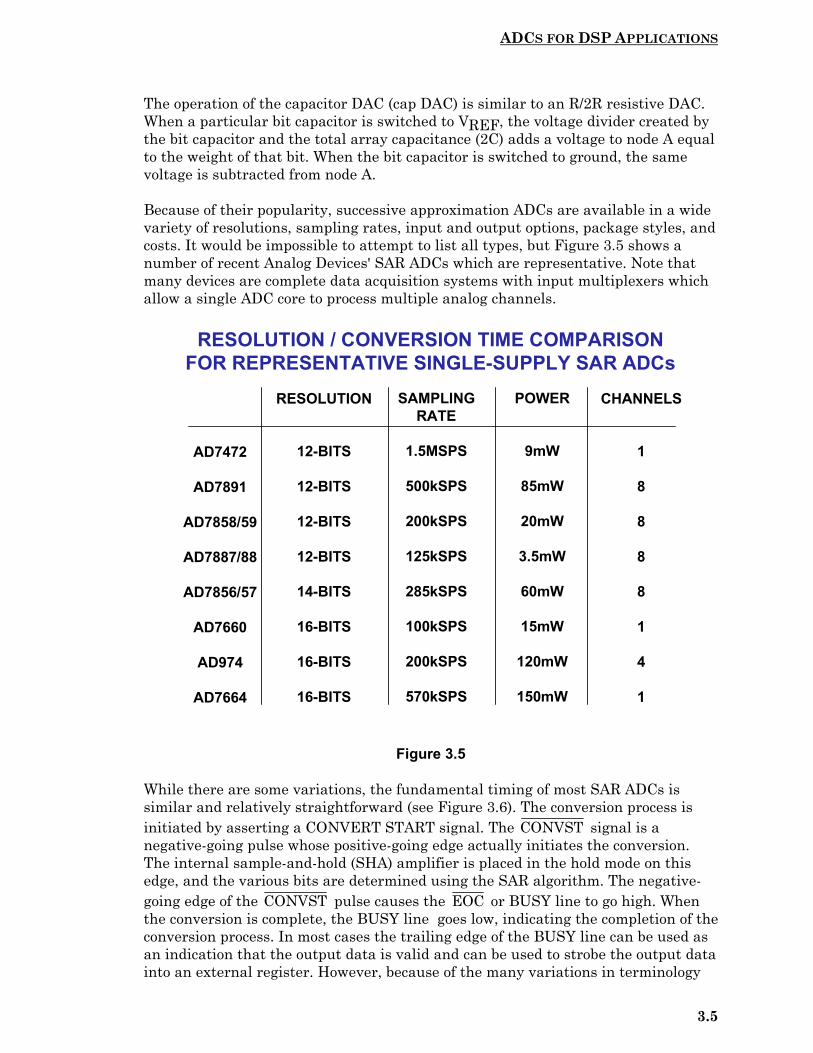
Because of their popularity, successive approximation ADCs are available in a widevariety of resolutions, sampling rates, input and output options, package styles, andcosts. It would be impossible to attempt to list all types, but Figure 3.5 shows anumber of recent Analog Devices' SAR ADCs which are representative. Note thatmany devices are complete data acquisition systems with input multiplexers whichallow a single ADC core to process multiple analog channels.
Figure 3.5
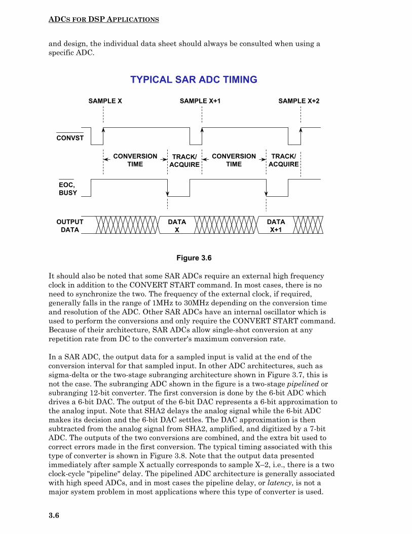
While there are some variations, the fundamental timing of most SAR ADCs issimilar and relatively straightforward (see Figure 3.6). The conversion process isinitiated by asserting a CONVERT START signal. The CONVST signal is anegative-going pulse whose positive-going edge actually initiates the conversion.The internal sample-and-hold (SHA) amplifier is placed in the hold mode on thisedge, and the various bits are determined using the SAR algorithm. The negative-going edge of the CONVST pulse causes the EOC or BUSY line to go high. Whenthe conversion is complete, the BUSY line goes low, indicating the completion of theconversion process. In most cases the trailing edge of the BUSY line can be used asan indication that the output data is valid and can be used to strobe the output datainto an external register. However, because of the many variations in terminology
RESOLUTION / CONVERSION TIME COMPARISONFOR REPRESENTATIVE SINGLE-SUPPLY SAR ADCs
AD7472
AD7891
AD7858/59
AD7887/88
AD7856/57
AD7660
AD974
AD7664
RESOLUTION
12-BITS
12-BITS
12-BITS
12-BITS
14-BITS
16-BITS
16-BITS
16-BITS
SAMPLINGRATE
1.5MSPS
500kSPS
200kSPS
125kSPS
285kSPS
100kSPS
200kSPS
570kSPS
POWER
9mW
85mW
20mW
3.5mW
60mW
15mW
120mW
150mW
CHANNELS
1
8
8
8
8
1
4
1
ADCS FOR DSP APPLICATIONS
3.6
and design, the individual data sheet should always be consulted when using aspecific ADC.
Figure 3.6
It should also be noted that some SAR ADCs require an external high frequencyclock in addition to the CONVERT START command. In most cases, there is noneed to synchronize the two. The frequency of the external clock, if required,generally falls in the range of 1MHz to 30MHz depending on the conversion timeand resolution of the ADC. Other SAR ADCs have an internal oscillator which isused to perform the conversions and only require the CONVERT START command.Because of their architecture, SAR ADCs allow single-shot conversion at anyrepetition rate from DC to the converter's maximum conversion rate.
In a SAR ADC, the output data for a sampled input is valid at the end of theconversion interval for that sampled input. In other ADC architectures, such assigma-delta or the two-stage subranging architecture shown in Figure 3.7, this isnot the case. The subranging ADC shown in the figure is a two-stage pipelined orsubranging 12-bit converter. The first conversion is done by the 6-bit ADC whichdrives a 6-bit DAC. The output of the 6-bit DAC represents a 6-bit approximation tothe analog input. Note that SHA2 delays the analog signal while the 6-bit ADCmakes its decision and the 6-bit DAC settles. The DAC approximation is thensubtracted from the analog signal from SHA2, amplified, and digitized by a 7-bitADC. The outputs of the two conversions are combined, and the extra bit used tocorrect errors made in the first conversion. The typical timing associated with thistype of converter is shown in Figure 3.8. Note that the output data presentedimmediately after sample X actually corresponds to sample X–2, i.e., there is a twoclock-cycle "pipeline" delay. The pipelined ADC architecture is generally associatedwith high speed ADCs, and in most cases the pipeline delay, or latency, is not amajor system problem in most applications where this type of converter is used.
TYPICAL SAR ADC TIMING
CONVST
CONVERSIONTIME
SAMPLE X SAMPLE X+1 SAMPLE X+2
DATAX
DATAX+1
OUTPUTDATA
EOC,BUSY
TRACK/ACQUIRE
CONVERSIONTIME
TRACK/ACQUIRE

ADCS FOR DSP APPLICATIONS
3.7
Figure 3.7
Figure 3.8
12-BIT TWO-STAGE PIPELINED ADC ARCHITECTURE
SHA1
SHA2
TIMING 6-BITADC
6-BITDAC
BUFFERREGISTER
+
_
7-BITADC
ERROR CORRECTION LOGIC
OUTPUT REGISTERS
6
6 7
12
12
ANALOGINPUT
SAMPLINGCLOCK
OUTPUT DATA
TYPICAL PIPELINED ADC TIMING
SAMPLINGCLOCK
SAMPLE X SAMPLE X+1 SAMPLE X+2
DATAX–2
DATAX–1
DATAX
OUTPUTDATA
ABOVE SHOWS TWO CLOCK-CYCLES PIPELINE DELAY
ADCS FOR DSP APPLICATIONS
3.8
Pipelined ADCs may have more than two clock-cycles latency depending on theparticular architecture. For instance, the conversion could be done in three, or four,or perhaps even more pipelined stages causing additional latency in the outputdata.
Therefore, if the ADC is to be used in an event-triggered (or single-shot) modewhere there must be a one-to-one time correspondence between each sample and thecorresponding data, then the pipeline delay can be troublesome, and the SARarchitecture is advantageous. Pipeline delay or latency can also be a problem inhigh speed servo-loop control systems or multiplexed applications. In addition, somepipelined converters have a minimum allowable conversion rate and must be keptrunning to prevent saturation of internal nodes.
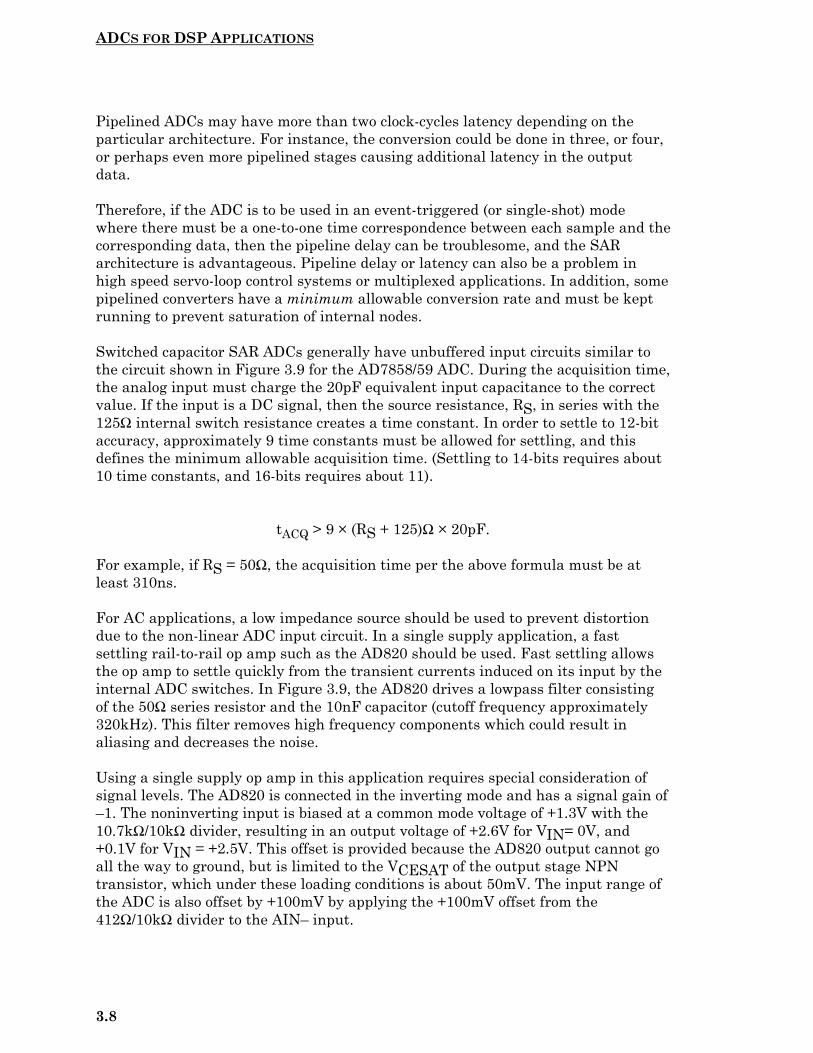
Switched capacitor SAR ADCs generally have unbuffered input circuits similar tothe circuit shown in Figure 3.9 for the AD7858/59 ADC. During the acquisition time,the analog input must charge the 20pF equivalent input capacitance to the correctvalue. If the input is a DC signal, then the source resistance, RS, in series with the125Ω internal switch resistance creates a time constant. In order to settle to 12-bitaccuracy, approximately 9 time constants must be allowed for settling, and thisdefines the minimum allowable acquisition time. (Settling to 14-bits requires about10 time constants, and 16-bits requires about 11).
tACQ > 9 × (RS + 125)Ω × 20pF.
For example, if RS = 50Ω, the acquisition time per the above formula must be atleast 310ns.
For AC applications, a low impedance source should be used to prevent distortiondue to the non-linear ADC input circuit. In a single supply application, a fastsettling rail-to-rail op amp such as the AD820 should be used. Fast settling allowsthe op amp to settle quickly from the transient currents induced on its input by theinternal ADC switches. In Figure 3.9, the AD820 drives a lowpass filter consistingof the 50Ω series resistor and the 10nF capacitor (cutoff frequency approximately320kHz). This filter removes high frequency components which could result inaliasing and decreases the noise.
Using a single supply op amp in this application requires special consideration ofsignal levels. The AD820 is connected in the inverting mode and has a signal gain of–1. The noninverting input is biased at a common mode voltage of +1.3V with the10.7kΩ/10kΩ divider, resulting in an output voltage of +2.6V for VIN= 0V, and+0.1V for VIN = +2.5V. This offset is provided because the AD820 output cannot goall the way to ground, but is limited to the VCESAT of the output stage NPNtransistor, which under these loading conditions is about 50mV. The input range ofthe ADC is also offset by +100mV by applying the +100mV offset from the412Ω/10kΩ divider to the AIN– input.

ADCS FOR DSP APPLICATIONS
3.9
Figure 3.9
SIGMA-DELTA (ΣΣΣΣ∆∆∆∆) ADCSJames M. BryantSigma-Delta Analog-Digital Converters (Σ∆ ADCs) have been known for nearlythirty years, but only recently has the technology (high-density digital VLSI) existedto manufacture them as inexpensive monolithic integrated circuits. They are nowused in many applications where a low-cost, low-bandwidth, low-power,high-resolution ADC is required.
There have been innumerable descriptions of the architecture and theory of Σ∆ADCs, but most commence with a maze of integrals and deteriorate from there. Inthe Applications Department at Analog Devices, we frequently encounter engineerswho do not understand the theory of operation of Σ∆ ADCs and are convinced, fromstudy of a typical published article, that it is too complex to comprehend easily.
There is nothing particularly difficult to understand about Σ∆ ADCs, as long as youavoid the detailed mathematics, and this section has been written in an attempt toclarify the subject. A Σ∆ ADC contains very simple analog electronics (a comparator,voltage reference, a switch, and one or more integrators and analog summingcircuits), and quite complex digital computational circuitry. This circuitry consists ofa digital signal processor (DSP) which acts as a filter (generally, but not invariably,
DRIVING SWITCHED CAPACITOR INPUTSOF AD7858/59 12-BIT, 200kSPS ADC
AD820
_
+
+
_
CAPDAC
10kΩΩΩΩ
10kΩΩΩΩ
10.7kΩΩΩΩ10kΩΩΩΩ
50ΩΩΩΩ
10nF
125ΩΩΩΩ
125ΩΩΩΩ
20pFT
H
H TVREF
AIN+
AIN–
DGND AGND
AVDD DVDD
0.1µF
0.1µF
+2.5V+1.30V
+3V TO +5V
VIN
VIN : 0V TO +2.5V
AIN+ : +2.6V TO +0.1VAD7858/59
CUTOFF= 320kHz
0.1µF
VCM =
NOTE: ONLY ONE INPUT SHOWN
T = TRACKH = HOLD
10kΩΩΩΩ
412ΩΩΩΩ +100mV
0.1µF
0.1µF

ADCS FOR DSP APPLICATIONS
3.10
a low pass filter). It is not necessary to know precisely how the filter works toappreciate what it does. To understand how a Σ∆ ADC works, familiarity with theconcepts of over-sampling, quantization noise shaping, digital filtering, anddecimation is required.
Figure 3.10
Let us consider the technique of over-sampling with an analysis in the frequencydomain. Where a DC conversion has a quantization error of up to ½ LSB, a sampleddata system has quantization noise. A perfect classical N-bit sampling ADC has anRMS quantization noise of q/√12 uniformly distributed within the Nyquist band ofDC to fs/2 (where q is the value of an LSB and fs is the sampling rate) as shown inFigure 3.11A. Therefore, its SNR with a full-scale sinewave input will be(6.02N + 1.76) dB. If the ADC is less than perfect, and its noise is greater than itstheoretical minimum quantization noise, then its effective resolution will be lessthan N-bits. Its actual resolution (often known as its Effective Number of Bits orENOB) will be defined by
ENOB SNR dBdB
= − 1766 02
..
.
If we choose a much higher sampling rate, Kfs (see Figure 3.11B), the RMSquantization noise remains q/√12, but the noise is now distributed over a widerbandwidth DC to Kfs/2. If we then apply a digital low pass filter (LPF) to theoutput, we remove much of the quantization noise, but do not affect the wanted
SIGMA-DELTA ADCs
Low Cost, High Resolution (to 24-bits)
Excellent DNL
Low Power, but Limited Bandwidth (Voiceband, Audio)
Key Concepts are Simple, but Math is Complex
Oversampling
Quantization Noise Shaping
Digital Filtering
Decimation
Ideal for Sensor Signal Conditioning
High Resolution
Self, System, and Auto Calibration Modes
Wide Applications in Voiceband and Audio SignalProcessing

ADCS FOR DSP APPLICATIONS
3.11
signal - so the ENOB is improved. We have accomplished a high resolution A/Dconversion with a low resolution ADC. The factor K is generally referred to as theoversampling ratio. It should be noted at this point that oversampling has an addedbenefit in that it relaxes the requirements on the analog antialiasing filter.
Figure 3.11
Since the bandwidth is reduced by the digital output filter, the output data rate maybe lower than the original sampling rate (Kfs) and still satisfy the Nyquist criterion.This may be achieved by passing every Mth result to the output and discarding theremainder. The process is known as "decimation" by a factor of M. Despite theorigins of the term (decem is Latin for ten), M can have any integer value, providedthat the output data rate is more than twice the signal bandwidth. Decimation doesnot cause any loss of information (see Figure 3.11B).
If we simply use over-sampling to improve resolution, we must over-sample by afactor of 22N to obtain an N-bit increase in resolution. The Σ∆ converter does notneed such a high over-sampling ratio because it not only limits the signal passband,but also shapes the quantization noise so that most of it falls outside this passbandas shown in Figure 3.11C.
If we take a 1-bit ADC (generally known as a comparator), drive it with the outputof an integrator, and feed the integrator with an input signal summed with theoutput of a 1-bit DAC fed from the ADC output, we have a first-order Σ∆ modulatoras shown in Figure 3.12. Add a digital low pass filter (LPF) and decimator at thedigital output, and we have a Σ∆ ADC: the Σ∆ modulator shapes the quantization
OVERSAMPLING, DIGITAL FILTERING,NOISE SHAPING, AND DECIMATION
fs2
fs
Kfs2
Kfs
KfsKfs2
fs2
fs2
DIGITAL FILTERREMOVED NOISE
REMOVED NOISE
QUANTIZATIONNOISE = q / 12 q = 1 LSBADC
ADC DIGITALFILTER
Σ∆Σ∆Σ∆Σ∆MOD
DIGITALFILTER
fs
Kfs
Kfs
DEC
fs
NyquistOperation
Oversampling+ Digital Filter+ Decimation
Oversampling+ Noise Shaping+ Digital Filter+ Decimation
A
B
C
DEC
fs

ADCS FOR DSP APPLICATIONS
3.12
noise so that it lies above the passband of the digital output filter, and the ENOB istherefore much larger than would otherwise be expected from the over-samplingratio.
Figure 3.12
Intuitively, a Σ∆ ADC operates as follows. Assume a DC input at VIN. Theintegrator is constantly ramping up or down at node A. The output of thecomparator is fed back through a 1-bit DAC to the summing input at node B. Thenegative feedback loop from the comparator output through the 1-bit DAC back tothe summing point will force the average DC voltage at node B to be equal to VIN.This implies that the average DAC output voltage must equal to the input voltageVIN. The average DAC output voltage is controlled by the ones-density in the 1-bitdata stream from the comparator output. As the input signal increases towards+VREF, the number of "ones" in the serial bit stream increases, and the number of"zeros" decreases. Similarly, as the signal goes negative towards –VREF, thenumber of "ones" in the serial bit stream decreases, and the number of "zeros"increases. From a very simplistic standpoint, this analysis shows that the averagevalue of the input voltage is contained in the serial bit stream out of thecomparator. The digital filter and decimator process the serial bit stream andproduce the final output data.
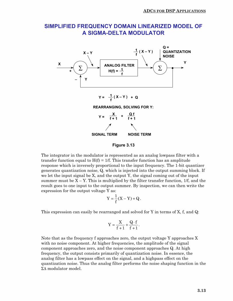
The concept of noise shaping is best explained in the frequency domain byconsidering the simple Σ∆ modulator model in Figure 3.13.
FIRST-ORDER SIGMA-DELTA ADC
∑ ∫ +
_
+VREF
–VREF
DIGITALFILTER
ANDDECIMATOR
+
_
CLOCKKfs
VINN-BITS
fs
fs
A
B
1-BIT DATASTREAM1-BIT
DAC
LATCHEDCOMPARATOR(1-BIT ADC)
1-BIT,Kfs
SIGMA-DELTA MODULATOR
INTEGRATOR
ADCS FOR DSP APPLICATIONS
3.13
Figure 3.13
The integrator in the modulator is represented as an analog lowpass filter with atransfer function equal to H(f) = 1/f. This transfer function has an amplituderesponse which is inversely proportional to the input frequency. The 1-bit quantizergenerates quantization noise, Q, which is injected into the output summing block. Ifwe let the input signal be X, and the output Y, the signal coming out of the inputsummer must be X – Y. This is multiplied by the filter transfer function, 1/f, and theresult goes to one input to the output summer. By inspection, we can then write theexpression for the output voltage Y as:
Yf
X Y Q= − +1 ( ) .
This expression can easily be rearranged and solved for Y in terms of X, f, and Q:
Y Xf
Q ff
=+
+ ⋅+1 1
.
Note that as the frequency f approaches zero, the output voltage Y approaches Xwith no noise component. At higher frequencies, the amplitude of the signalcomponent approaches zero, and the noise component approaches Q. At highfrequency, the output consists primarily of quantization noise. In essence, theanalog filter has a lowpass effect on the signal, and a highpass effect on thequantization noise. Thus the analog filter performs the noise shaping function in theΣ∆ modulator model.
SIMPLIFIED FREQUENCY DOMAIN LINEARIZED MODEL OFA SIGMA-DELTA MODULATOR
∑ ANALOG FILTERH(f) = 1
f∑
X Y
+
_
X – Y1f
( X – Y )Q = QUANTIZATIONNOISE
Y = 1f
( X – Y ) + Q
REARRANGING, SOLVING FOR Y:
Y = X
f + 1 + Q ff + 1
SIGNAL TERM NOISE TERM
Y

ADCS FOR DSP APPLICATIONS
3.14
For a given input frequency, higher order analog filters offer more attenuation. Thesame is true of Σ∆ modulators, provided certain precautions are taken.
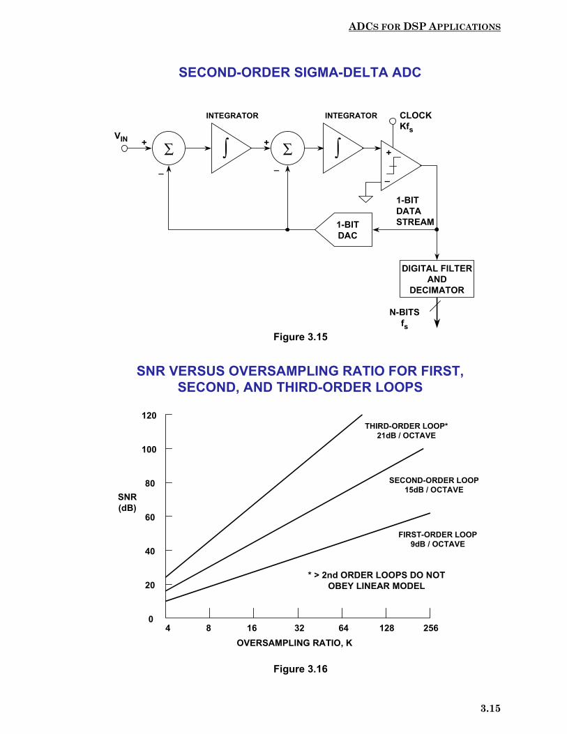
By using more than one integration and summing stage in the Σ∆ modulator, we canachieve higher orders of quantization noise shaping and even better ENOB for agiven over-sampling ratio as is shown in Figure 3.14 for both a first and second-order Σ∆ modulator. The block diagram for the second-order Σ∆ modulator is shownin Figure 3.15. Third, and higher, order Σ∆ ADCs were once thought to bepotentially unstable at some values of input - recent analyses using finite ratherthan infinite gains in the comparator have shown that this is not necessarily so, buteven if instability does start to occur, it is not important, since the DSP in thedigital filter and decimator can be made to recognize incipient instability and reactto prevent it.
Figure 3.16 shows the relationship between the order of the Σ∆ modulator and theamount of over-sampling necessary to achieve a particular SNR. For instance, if theoversampling ratio is 64, an ideal second-order system is capable of providing anSNR of about 80dB. This implies approximately 13 effective number of bits (ENOB).Although the filtering done by the digital filter and decimator can be done to anydegree of precision desirable, it would be pointless to carry more than 13 binary bitsto the outside world. Additional bits would carry no useful signal information, andwould be buried in the quantization noise unless post-filtering techniques wereemployed. Additional resolution can be obtained by increasing the oversamplingratio and/or by using a higher-order modulator.
Figure 3.14
SIGMA-DELTA MODULATORSSHAPE QUANTIZATION NOISE
fs2
Kfs2
2ND ORDER
1ST ORDER
DIGITALFILTER
ADCS FOR DSP APPLICATIONS
3.15
Figure 3.15
Figure 3.16
SECOND-ORDER SIGMA-DELTA ADC
∑ ∫+
_
VIN
INTEGRATOR
∑ ∫ +
_
CLOCKKfs
1-BITDAC
INTEGRATOR
DIGITAL FILTERAND
DECIMATOR
N-BITSfs
+
_
1-BITDATASTREAM
SNR VERSUS OVERSAMPLING RATIO FOR FIRST,SECOND, AND THIRD-ORDER LOOPS
FIRST-ORDER LOOP9dB / OCTAVE
SECOND-ORDER LOOP15dB / OCTAVE
THIRD-ORDER LOOP*21dB / OCTAVE
* > 2nd ORDER LOOPS DO NOTOBEY LINEAR MODEL
4 8 16 32 64 128 2560
20
40
60
80
100
120
SNR(dB)
OVERSAMPLING RATIO, K

ADCS FOR DSP APPLICATIONS
3.16
The AD1877 is a 16-bit 48kSPS stereo sigma-delta DAC suitable for demandingaudio applications. Key specifications are summarized in Figure 3.17. This devicehas a 64X oversampling ratio, and a fourth-order modulator. The internal digitalfilter is a linear phase FIR filter whose response is shown in Figure 3.18. Thepassband ripple is 0.006dB, and the attenuation is greater than 90dB in thestopband. The width of the transition region from passband to stopband is only0.1fs, where fs is the effective sampling frequency of the AD1877 (maximum of48kSPS). Such a filter would obviously be impossible to implement in analog form.
Figure 3.17
All sigma-delta ADCs have a settling time associated with the internal digital filter,and there is no way to remove it. In multiplexed applications the input to the ADCis a step function if there are different input voltages on adjacent channels. In fact,the multiplexer output can represent a fullscale step voltage to the sigma-delta ADCwhen channels are switched. Adequate filter settling time must be allowed,therefore, in such applications. This does not mean that sigma-delta ADCsshouldn’t be used in multiplexed applications, just that the settling time of thedigital filter must be considered.
For example, the group delay through the AD1877 FIR filter is 36/fs, andrepresents the time it takes for a step function input to propagate through one-halfthe number of taps in the digital filter. The total time required for settling istherefore 72fs, or approximately 1.5ms when sampling at 48kSPS with a 64Xoversampling rate.
AD1877 16-BIT, 48kSPS STEREO SIGMA-DELTA ADC
Single +5 V Power Supply Single-Ended Dual-Channel Analog Inputs 92 dB (typ) Dynamic Range 90 dB (typ) S/(THD+N) 0.006 dB Decimator Passband Ripple Fourth-Order, 64-Times Oversampling Σ∆Σ∆Σ∆Σ∆ Modulator Three-Stage, Linear-Phase Decimator Less than 100 mW (typ) Power-Down Mode Input Overrange Indication On-Chip Voltage Reference Flexible Serial Output Interface 28-Pin SOIC Package

ADCS FOR DSP APPLICATIONS
3.17
Figure 3.18
In other applications, such as low frequency, high resolution 24-bit measurementsigma-delta ADCs (such as the AD77xx-series), other types of digital filters may beused. For instance, the SINC3 response is popular because it has zeros at multiplesof the throughput rate. For instance a 10Hz throughput rate produces zeros at50Hz and 60Hz which aid in AC power line rejection.
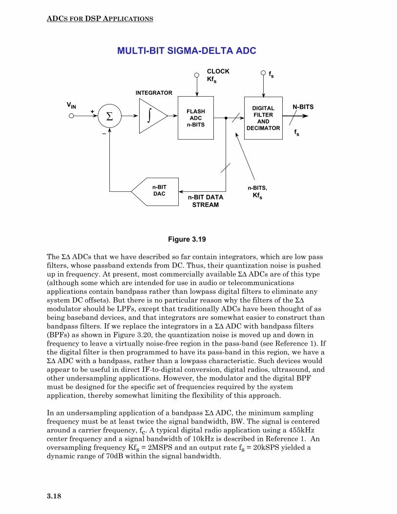
So far we have considered only sigma-delta converters which contain a single-bitADC (comparator) and a single-bit DAC (switch). The block diagram of Figure 3.19shows a multi-bit sigma-delta ADC which uses an n-bit flash ADC and an n-bitDAC. Obviously, this architecture will give a higher dynamic range for a givenoversampling ratio and order of loop filter. Stabilization is easier, since second-orderand higher loops can be used. Idling patterns tend to be more random therebyminimizing tonal effects.
The real disadvantage of this technique is that the linearity depends on the DAClinearity, and thin film laser trimming is generally required to approach 16-bitperformance levels. This makes the multi-bit architecture extremely difficult toimplement on sigma-delta ADCs. It is, however, currently used in sigma-delta audioDACs (AD1852, AD1853, AD1854) where special “bit scrambling” techniques areused to ensure linearity and eliminate idle tones.
AD1877 16-BIT, 48kSPS STEREO SIGMA-DELTA ADCFIR FILTER CHARACTERISTICS
fs = OUTPUT WORD RATE, 32kSPS, 44.1kSPS, OR 48kSPS TYPICAL PASSBAND TO STOPBAND TRANSITION REGION: 0.45fs TO 0.55fs SETTLING TIME = 72 / fs = 1.5ms FOR fs = 48kSPS GROUP DELAY = 36 / fs = 0.75ms FOR fs = 48kSPS
NORMALIZED fs
ADCS FOR DSP APPLICATIONS
3.18
Figure 3.19
The Σ∆ ADCs that we have described so far contain integrators, which are low passfilters, whose passband extends from DC. Thus, their quantization noise is pushedup in frequency. At present, most commercially available Σ∆ ADCs are of this type(although some which are intended for use in audio or telecommunicationsapplications contain bandpass rather than lowpass digital filters to eliminate anysystem DC offsets). But there is no particular reason why the filters of the Σ∆modulator should be LPFs, except that traditionally ADCs have been thought of asbeing baseband devices, and that integrators are somewhat easier to construct thanbandpass filters. If we replace the integrators in a Σ∆ ADC with bandpass filters(BPFs) as shown in Figure 3.20, the quantization noise is moved up and down infrequency to leave a virtually noise-free region in the pass-band (see Reference 1). Ifthe digital filter is then programmed to have its pass-band in this region, we have aΣ∆ ADC with a bandpass, rather than a lowpass characteristic. Such devices wouldappear to be useful in direct IF-to-digital conversion, digital radios, ultrasound, andother undersampling applications. However, the modulator and the digital BPFmust be designed for the specific set of frequencies required by the systemapplication, thereby somewhat limiting the flexibility of this approach.
In an undersampling application of a bandpass Σ∆ ADC, the minimum samplingfrequency must be at least twice the signal bandwidth, BW. The signal is centeredaround a carrier frequency, fc. A typical digital radio application using a 455kHzcenter frequency and a signal bandwidth of 10kHz is described in Reference 1. Anoversampling frequency Kfs = 2MSPS and an output rate fs = 20kSPS yielded adynamic range of 70dB within the signal bandwidth.
MULTI-BIT SIGMA-DELTA ADC
∑ ∫DIGITALFILTER
ANDDECIMATOR
+
_
CLOCKKfs
VIN N-BITS
fs
fs
n-BIT DATASTREAM
n-BITS,Kfs
INTEGRATOR
FLASHADC
n-BITS
n-BITDAC

ADCS FOR DSP APPLICATIONS
3.19
Figure 3.20
Most sigma-delta ADCs generally have a fixed internal digital filter. The filter’scutoff frequency and the ADC output data rate scales with the master clockfrequency. The AD7725 is a 16-bit sigma-delta ADC with a programmable internaldigital filter. The modulator operates at a maximum oversampling rate of19.2MSPS. The modulator is followed by a preset FIR filter which decimates themodulator output by a factor of 8, yielding an output data rate of 2.4MSPS. Theoutput of the preset filter drives a programmable FIR filter. By loading the ROMwith suitable coefficient values, this filter can be programmed for the desiredfrequency response.
The programmable filter is flexible with respect to number of taps and decimationrate. The filter can have up to 108 taps, up to 5 decimation stages, and a decimationfactor between 2 and 256. Coefficient precision is 24-bits, and arithmetic precision is30-bits.
The AD7725 contains Systolix’s PuldeDSP™ (trademark of Systolix) post processorwhich permits the filter characteristics to be programmed through the parallel orserial microprocessor interface. Or, it may boot at power-on-reset from its internalROM or from an external EPROM.
REPLACING INTEGRATORS WITH RESONATORSGIVES A BANDPASS SIGMA-DELTA ADC
ΣΣΣΣ ΣΣΣΣ+
-
+
-
1-BITDAC
ANALOGBPF
ANALOGBPF DIGITAL
BPF ANDDECIMATOR
CLOCK Kfs
fs
SHAPEDQUANTIZATION
NOISE
DIGITAL BPFRESPONSEfc
f
BW fs > 2 BW

ADCS FOR DSP APPLICATIONS
3.20
The post processor is a fully programmable core which provides processing power ofup to 130 million multiply-accumulates (MAC) per second. To program the postprocessor, the user must produce a configuration file which contains theprogramming data for the filter function. This file is generated by a compiler whichis available from Analog Devices. The AD7725 compiler accepts filter coefficientdata as an input and automatically generates the required device programmingdata.
The coefficient file for the FIR filter response can be generated using a digital filterdesign package such as QEDesign from Momentum Data Systems. The response ofthe filter can be plotted so the user knows the response before generating the filtercoefficients. The data is available to the processor at a 2.4MSPS rate. Whendecimation is employed in a multistage filter, the first filter will be operated at2.4MSPS, and the user can then decimate between stages. The number of tapswhich can be contained in the processor is 108. Therefore, a single filter with 108taps can be generated, or a multistage filter can be designed whereby the totalnumber of taps adds up to 108. The filter characteristic can be lowpass, highpass,bandstop, or bandpass.
The AD7725 operates on a single +5V supply, has an on-chip 2.5V reference, and ispackaged in a 44-pin PQFP. Power dissipation is approximately 350mW whenoperating at full power. A half-power mode is available with a master clockfrequency of 10MSPS maximum. Power consumption in the standby mode is 200mWmaximum. More details of the AD7725 operation can be found in Section 9.
Summary
A Σ∆ ADC works by over-sampling, where simple analog filters in the Σ∆ modulatorshape the quantization noise so that the SNR in the bandwidth of interest is muchgreater than would otherwise be the case, and by using high performance digitalfilters and decimation to eliminate noise outside the required passband.Oversampling has the added benefit of relaxing the requirements on theantialiasing filter. Because the analog circuitry is relatively undemanding, it may bebuilt with the same digital VLSI process that is used to fabricate the DSP circuitryof the digital filter. Because the basic ADC is 1-bit (a comparator), the technique isinherently linear.
Although the detailed analysis of Σ∆ ADCs involves quite complex mathematics,their basic design can be understood without the necessity of any mathematics atall. For further discussion on Σ∆ ADCs, refer to References 1 through 18 at the endof this section.
ADCS FOR DSP APPLICATIONS
3.21
Figure 3.21
FLASH CONVERTERS
Flash ADCs (sometimes called parallel ADCs) are the fastest type of ADC and uselarge numbers of comparators. An N-bit flash ADC consists of 2N resistors and 2N–1comparators arranged as in Figure 3.22. Each comparator has a reference voltagewhich is 1 LSB higher than that of the one below it in the chain. For a given inputvoltage, all the comparators below a certain point will have their input voltagelarger than their reference voltage and a "1" logic output, and all the comparatorsabove that point will have a reference voltage larger than the input voltage and a"0" logic output. The 2N–1 comparator outputs therefore behave in a way analogousto a mercury thermometer, and the output code at this point is sometimes called athermometer code. Since 2N–1 data outputs are not really practical, they areprocessed by a decoder to an N-bit binary output.
The input signal is applied to all the comparators at once, so the thermometeroutput is delayed by only one comparator delay from the input, and the encoderN-bit output by only a few gate delays on top of that, so the process is very fast.However, the architecture uses large numbers of resistors and comparators and islimited to low resolutions, and if it is to be fast, each comparator must run atrelatively high power levels. Hence, the problems of flash ADCs include limitedresolution, high power dissipation because of the large number of high speedcomparators (especially at sampling rates greater than 50MSPS), and relativelylarge (and therefore expensive) chip sizes. In addition, the resistance of thereference resistor chain must be kept low to supply adequate bias current to the fastcomparators, so the voltage reference has to source quite large currents (>10 mA).
SIGMA-DELTA SUMMARY
Inherently Excellent Linearity Oversampling Relaxes Analog Antialiasing Filter Requirements Ideal for Mixed-Signal IC Processes, no Trimming No SHA Required Added Functionality: On-Chip PGAs, Analog Filters,
Autocalibration On-Chip Programmable Digital Filters (AD7725: Lowpass,
Highpass, Bandpass, Bandstop) Upper Sampling Rate Currently Limits Applications to
Measurement, Voiceband, and Audio, but Bandpass Sigma-DeltaTechniques May Change This
Analog Multiplexer Switching Speed Limited by Internal FilterSettling Time. Consider One Sigma-Delta ADC per Channel.

ADCS FOR DSP APPLICATIONS
3.22
In practice, flash converters are available up to 10-bits, but more commonly theyhave 8-bits of resolution. Their maximum sampling rate can be as high as 1GHz,with input full-power bandwidths in excess of 300 MHz.
Figure 3.22
But as mentioned earlier, full-power bandwidths are not necessarily full-resolutionbandwidths. Ideally, the comparators in a flash converter are well matched both forDC and AC characteristics. Because the strobe is applied to all the comparatorssimultaneously, the flash converter is inherently a sampling converter. In practice,there are delay variations between the comparators and other AC mismatcheswhich cause a degradation in ENOB at high input frequencies. This is because theinputs are slewing at a rate comparable to the comparator conversion time.
The input to a flash ADC is applied in parallel to a large number of comparators.Each has a voltage-variable junction capacitance, and this signal-dependentcapacitance results in most flash ADCs having reduced ENOB and higher distortionat high input frequencies.
Adding 1 bit to the total resolution of a flash converter requires doubling thenumber of comparators! This limits the practical resolution of high speed flashconverters to 8-bits because of excessive power dissipation.
FLASH OR PARALLEL ADC
N
R
PRIORITYENCODER
AND LATCH
ANALOGINPUT
DIGITALOUTPUT
+VREF
R
R
R
R
R
0.5R
STROBE
1.5R

ADCS FOR DSP APPLICATIONS
3.23
However, in the AD9410 10-bit, 200MSPS ADC, a technique called interpolation isused to minimize the number of preamplifiers in the flash converter comparatorsand also reduce the power (1.8W). The method is shown in Figure 3.23.
Figure 3.23
The preamplifiers (labeled “A1”, “A2”, etc.) are low-gain gm stages whose bandwidthis proportional to the tail currents of the differential pairs. Consider the case for apositive-going ramp input which is initially below the reference to AMP A1, V1. Asthe input signal approaches V1, the differential output of A1 approaches zero (i.e., A= A ), and the decision point is reached. The output of A1 drives the differentialinput of LATCH 1. As the input signals continues to go positive, A continues to gopositive, and B begins to go negative. The interpolated decision point is determinedwhen A = B . As the input continues positive, the third decision point is reachedwhen B = B . This novel architecture reduces the ADC input capacitance andthereby minimizes its change with signal level and the associated distortion. TheAD9410 also uses an input sample-and-hold circuit for improved AC linearity.
SUBRANGING (PIPELINED) ADCS
Although it is not practical to make flash ADCs with high resolution (greater than10-bits), flash ADCs are often used as subsystems in "subranging" ADCs (sometimesknown as "half-flash ADCs"), which are capable of much higher resolutions (up to16-bits).
“INTERPOLATING” FLASH REDUCES THE NUMBEROF PREAMPLIFIERS BY FACTOR OF TWO
B
V1A =
A2
LATCHSTROBE
ANALOGINPUT ANALOG
INPUT
DECODE
LATCH2
LATCH1A
LATCH1
A
B
V2
V1 AA1
+
+
-
-
B
B
B
B
V1A
V1
A
A
A
A
V2
V1 + V22
AD9410: 10-Bits, 200MSPS

ADCS FOR DSP APPLICATIONS
3.24
A block diagram of an 8-bit subranging ADC based upon two 4-bit flash convertersis shown in Figure 3.24. Although 8-bit flash converters are readily available athigh sampling rates, this example will be used to illustrate the theory. Theconversion process is done in two steps. The first four significant bits (MSBs) aredigitized by the first flash (to better than 8-bits accuracy), and the 4-bit binaryoutput is applied to a 4-bit DAC (again, better than 8-bit accurate). The DAC outputis subtracted from the held analog input, and the resulting residue signal isamplified and applied to the second 4-bit flash. The outputs of the two 4-bit flashconverters are then combined into a single 8-bit binary output word. If the residuesignal range does not exactly fill the range of the second flash converter, non-linearities and perhaps missing codes will result.
Figure 3.24
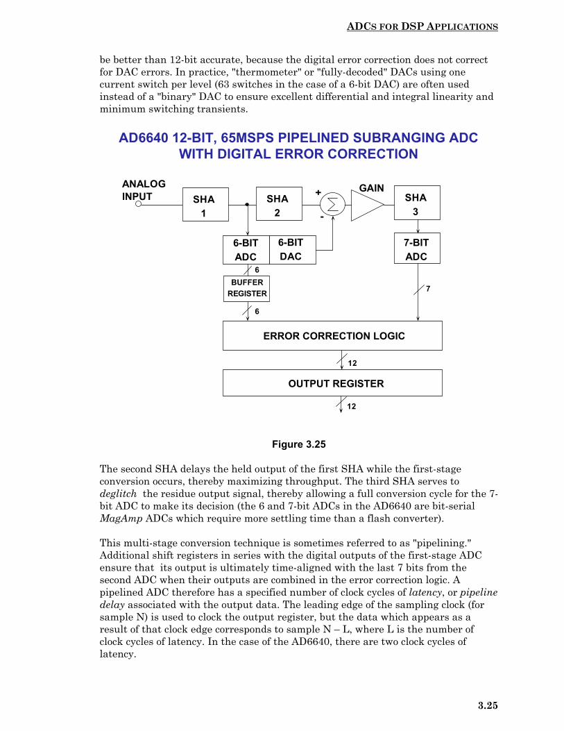
Modern subranging ADCs use a technique called digital correction to eliminateproblems associated with the architecture of Figure 3.24. A simplified block diagramof a 12-bit digitally corrected subranging (DCS) ADC is shown in Figure 3.25. Thearchitecture is similar to that used in the AD6640 12-bit, 65MSPS ADC. Note that a6-bit and an 7-bit ADC have been used to achieve an overall 12-bit output. Theseare not flash ADCs, but utilize a magnitude-amplifier (MagAmp™) architecturewhich will be described shortly.
If there were no errors in the first-stage conversion, the 6-bit "residue" signalapplied to the 7-bit ADC by the summing amplifier would never exceed one-half ofthe range of the 7-bit ADC. The extra range in the second ADC is used inconjunction with the error correction logic (usually just a full adder) to correct theoutput data for most of the errors inherent in the traditional uncorrectedsubranging converter architecture. It is important to note that the 6-bit DAC must
8-BIT SUBRANGING ADC
ANALOGINPUT
4
8
SHA
4-BITFLASH
4-BITDAC
4-BITFLASH
GAIN
4
+
-RESIDUESIGNAL
OUTPUT REGISTER
ADCS FOR DSP APPLICATIONS
3.25
be better than 12-bit accurate, because the digital error correction does not correctfor DAC errors. In practice, "thermometer" or "fully-decoded" DACs using onecurrent switch per level (63 switches in the case of a 6-bit DAC) are often usedinstead of a "binary" DAC to ensure excellent differential and integral linearity andminimum switching transients.
Figure 3.25
The second SHA delays the held output of the first SHA while the first-stageconversion occurs, thereby maximizing throughput. The third SHA serves todeglitch the residue output signal, thereby allowing a full conversion cycle for the 7-bit ADC to make its decision (the 6 and 7-bit ADCs in the AD6640 are bit-serialMagAmp ADCs which require more settling time than a flash converter).
This multi-stage conversion technique is sometimes referred to as "pipelining."Additional shift registers in series with the digital outputs of the first-stage ADCensure that its output is ultimately time-aligned with the last 7 bits from thesecond ADC when their outputs are combined in the error correction logic. Apipelined ADC therefore has a specified number of clock cycles of latency, or pipelinedelay associated with the output data. The leading edge of the sampling clock (forsample N) is used to clock the output register, but the data which appears as aresult of that clock edge corresponds to sample N – L, where L is the number ofclock cycles of latency. In the case of the AD6640, there are two clock cycles oflatency.
AD6640 12-BIT, 65MSPS PIPELINED SUBRANGING ADCWITH DIGITAL ERROR CORRECTION
ANALOGINPUT
7
12
SHA1
6-BITADC
7-BITADC
GAIN
6
+
-
ERROR CORRECTION LOGIC
6-BITDAC
SHA2
SHA3
OUTPUT REGISTER
12
BUFFERREGISTER
6
ADCS FOR DSP APPLICATIONS
3.26
The error correction scheme described above is designed to correct for errors madein the first conversion. Internal ADC gain, offset, and linearity errors are correctedas long as the residue signal falls within the range of the second-stage ADC. Theseerrors will not affect the linearity of the overall ADC transfer characteristic. Errorsmade in the final conversion, however, do translate directly as errors in the overalltransfer function. Also, linearity errors or gain errors either in the DAC or theresidue amplifier will not be corrected and will show up as nonlinearities or non-monotonic behavior in the overall ADC transfer function.
So far, we have considered only two-stage subranging ADCs, as these are easiest toanalyze. There is no reason to stop at two stages, however. Three-pass and four-passsubranging pipelined ADCs are quite common, and can be made in many differentways, usually with digital error correction.
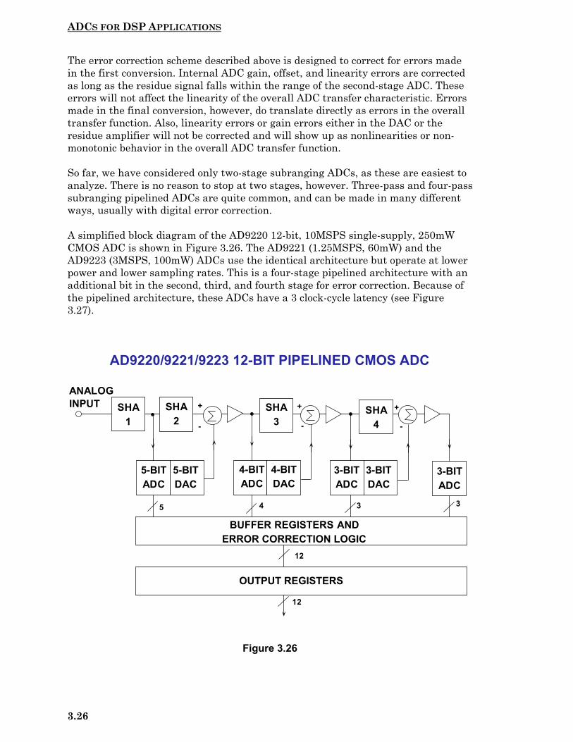
A simplified block diagram of the AD9220 12-bit, 10MSPS single-supply, 250mWCMOS ADC is shown in Figure 3.26. The AD9221 (1.25MSPS, 60mW) and theAD9223 (3MSPS, 100mW) ADCs use the identical architecture but operate at lowerpower and lower sampling rates. This is a four-stage pipelined architecture with anadditional bit in the second, third, and fourth stage for error correction. Because ofthe pipelined architecture, these ADCs have a 3 clock-cycle latency (see Figure3.27).
Figure 3.26
AD9220/9221/9223 12-BIT PIPELINED CMOS ADC
ANALOGINPUT + + +
- - -
5 4 3 3
12
12
BUFFER REGISTERS ANDERROR CORRECTION LOGIC
OUTPUT REGISTERS
SHA1
SHA2
SHA3
SHA4
5-BITADC
5-BITDAC
4-BITADC
4-BITDAC
3-BITADC
3-BITDAC
3-BITADC

ADCS FOR DSP APPLICATIONS
3.27
Figure 3.27
BIT-PER-STAGE (SERIAL, OR RIPPLE) ADCS
Various architectures exist for performing A/D conversion using one stage per bit. Infact, a multistage subranging ADC with one bit per stage and no error correction isone form. Figure 3.28 shows the overall concept. The SHA holds the input signalconstant during the conversion cycle. There are N stages, each of which have a bitoutput and a residue output. The residue output of one stage is the input to thenext. The last bit is detected with a single comparator as shown.
Figure 3.28
LATENCY (PIPELINE DELAY)OF AD9220/9221/9223 ADC
ANALOGINPUT
SAMPLINGCLOCK
OUTPUTDATA DATA N - 3 DATA N - 2 DATA N - 1 DATA N
N N + 1 N + 2 N + 3
BIT-PER-STAGE, SERIAL, OR RIPPLE ADC
ANALOGINPUT
SHA STAGE1
STAGE2
DECODE LOGIC AND OUTPUT REGISTERS
+
-BIT 1MSB
BIT 2
VREF
N
R1 R2 STAGEN-1
BIT N-1 BIT NLSB
ADCS FOR DSP APPLICATIONS
3.28
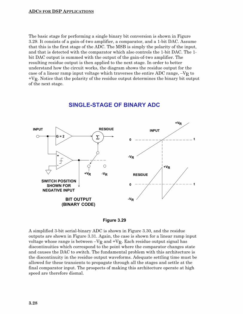
The basic stage for performing a single binary bit conversion is shown in Figure3.29. It consists of a gain-of-two amplifier, a comparator, and a 1-bit DAC. Assumethat this is the first stage of the ADC. The MSB is simply the polarity of the input,and that is detected with the comparator which also controls the 1-bit DAC. The 1-bit DAC output is summed with the output of the gain-of-two amplifier. Theresulting residue output is then applied to the next stage. In order to betterunderstand how the circuit works, the diagram shows the residue output for thecase of a linear ramp input voltage which traverses the entire ADC range, –VR to+VR. Notice that the polarity of the residue output determines the binary bit outputof the next stage.
Figure 3.29
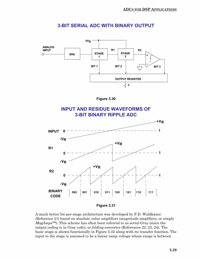
A simplified 3-bit serial-binary ADC is shown in Figure 3.30, and the residueoutputs are shown in Figure 3.31. Again, the case is shown for a linear ramp inputvoltage whose range is between –VR and +VR. Each residue output signal hasdiscontinuities which correspond to the point where the comparator changes stateand causes the DAC to switch. The fundamental problem with this architecture isthe discontinuity in the residue output waveforms. Adequate settling time must beallowed for these transients to propagate through all the stages and settle at thefinal comparator input. The prospects of making this architecture operate at highspeed are therefore dismal.
SINGLE-STAGE OF BINARY ADC
INPUT INPUTRESIDUE
+VR
+VR
-VR
-VR
0
0
RESIDUE+VR -VR
G = 2
+
-
Σ
BIT OUTPUT(BINARY CODE)
SWITCH POSITIONSHOWN FOR
NEGATIVE INPUT
t
t
ADCS FOR DSP APPLICATIONS
3.29
Figure 3.30
Figure 3.31
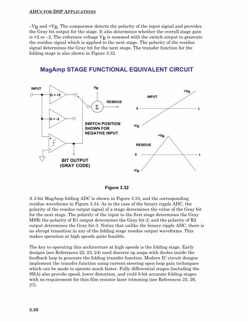
A much better bit-per-stage architecture was developed by F.D. Waldhauer(Reference 21) based on absolute value amplifiers (magnitude amplifiers, or simplyMagAmps™). This scheme has often been referred to as serial-Gray (since theoutput coding is in Gray code), or folding converter (References 22, 23, 24). Thebasic stage is shown functionally in Figure 3.32 along with its transfer function. Theinput to the stage is assumed to be a linear ramp voltage whose range is between
3-BIT SERIAL ADC WITH BINARY OUTPUT
ANALOGINPUT
SHA STAGE1
STAGE2
OUTPUT REGISTER
+
-BIT 1 BIT 2 BIT 3
±VR
3
R1 R2
INPUT AND RESIDUE WAVEFORMS OF3-BIT BINARY RIPPLE ADC
INPUT
R1
R2
BINARYCODE
-VR
-VR
-VR
+VR
+VR
+VR
000 001 010 011 100 101 110 111
0
0
0
t
t
t
ADCS FOR DSP APPLICATIONS
3.30
–VR and +VR. The comparator detects the polarity of the input signal and providesthe Gray bit output for the stage. It also determines whether the overall stage gainis +2 or –2. The reference voltage VR is summed with the switch output to generatethe residue signal which is applied to the next stage. The polarity of the residuesignal determines the Gray bit for the next stage. The transfer function for thefolding stage is also shown in Figure 3.32.
Figure 3.32
A 3-bit MagAmp folding ADC is shown in Figure 3.33, and the correspondingresidue waveforms in Figure 3.34. As in the case of the binary ripple ADC, thepolarity of the residue output signal of a stage determines the value of the Gray bitfor the next stage. The polarity of the input to the first stage determines the GrayMSB; the polarity of R1 output determines the Gray bit-2; and the polarity of R2output determines the Gray bit-3. Notice that unlike the binary ripple ADC, there isno abrupt transition in any of the folding stage residue output waveforms. Thismakes operation at high speeds quite feasible.
The key to operating this architecture at high speeds is the folding stage. Earlydesigns (see References 22, 23, 24) used discrete op amps with diodes inside thefeedback loop to generate the folding transfer function. Modern IC circuit designsimplement the transfer function using current-steering open-loop gain techniqueswhich can be made to operate much faster. Fully differential stages (including theSHA) also provide speed, lower distortion, and yield 8-bit accurate folding stageswith no requirement for thin film resistor laser trimming (see References 25, 26,27).
MagAmp STAGE FUNCTIONAL EQUIVALENT CIRCUIT
INPUT
G = +2 INPUTRESIDUE
+VR
+VR
-VR
-VR
0
0
RESIDUE
VR
+
-
BIT OUTPUT(GRAY CODE)
G = -2
Σ
SWITCH POSITIONSHOWN FORNEGATIVE INPUT
t
t

ADCS FOR DSP APPLICATIONS
3.31
Figure 3.33
Figure 3.34
3-BIT MagAmp™ (FOLDING) ADC BLOCK DIAGRAM
ANALOGINPUT
SHA MAGAMP1
MAGAMP2
GRAY-TO-BINARY CONVERTER
OUTPUT REGISTER
GRAY CODE REGISTER
+
-BIT 1 BIT 2 BIT 3
±VR
3
3
3
INPUT AND RESIDUE WAVEFORMSFOR 3-BIT MagAmp ADC
INPUT
R1
R2
GRAYCODE
-VR
-VR
-VR
+VR
+VR
+VR
000 001 011 010 110 111 101 100
0
0
0
t
t
t

ADCS FOR DSP APPLICATIONS
3.32
The MagAmp architecture can be extended to sampling rates previously dominatedby flash converters. The AD9288-100 8-bit, 100MSPS dual ADC is shown in Figure3.35. The first five bits (Gray code) are derived from five differential MagAmpstages. The differential residue output of the fifth MagAmp stage drives a 3-bitflash converter, rather than a single comparator. The Gray-code output of the fiveMagAmps and the binary-code output of the 3-bit flash are latched, all convertedinto binary, and latched again in the output data register.
Figure 3.35
AD9288-100 DUAL 8-BIT,100MSPS ADC FUNCTIONAL DIAGRAM
5
5
8
ANALOGINPUT
SHA MAGAMP1
MAGAMP2
MAGAMP3
MAGAMP4
MAGAMP5
3-BITFLASH
ADC
BIT1
GRAY
BIT2
GRAY
BIT3
GRAY
BIT4
GRAY
BIT5
GRAY
3
REGISTER
GRAY-TO-BINARY CONVERTER
OUTPUT REGISTER
BINARYDIFFERENTIALOUTPUTS ONBITS 1 - 5
3

ADCS FOR DSP APPLICATIONS
3.33
REFERENCES
1. S. A. Jantzi, M. Snelgrove & P. F. Ferguson Jr., A 4th-Order BandpassSigma-Delta Modulator, IEEE Journal of Solid State Circuits,Vol. 38, No. 3, March 1993, pp.282-291.
2. System Applications Guide, Analog Devices, Inc., 1993, Section 14.
3. Mixed Signal Design Seminar, Analog Devices, Inc., 1991, Section 6.
4. AD77XX-Series Data Sheets, Analog Devices, http://www.analog.com.
5. Linear Design Seminar, Analog Devices, Inc., 1995, Section 8.
6. J. Dattorro, A. Charpentier, D. Andreas, The Implementation of a One-Stage Multirate 64:1 FIR Decimator for use in One-Bit Sigma-Delta A/DApplications, AES 7th International Conference, May 1989.
7. W.L. Lee and C.G. Sodini, A Topology for Higher-Order InterpolativeCoders, ISCAS PROC. 1987.
8. P.F. Ferguson, Jr., A. Ganesan and R. W. Adams, One Bit Higher OrderSigma-Delta A/D Converters, ISCAS PROC. 1990, Vol. 2, pp. 890-893.
9. R. Koch, B. Heise, F. Eckbauer, E. Engelhardt, J. Fisher, and F. Parzefall,A 12-bit Sigma-Delta Analog-to-Digital Converter with a 15MHz ClockRate, IEEE Journal of Solid-State Circuits, Vol. SC-21, No. 6,December 1986.
10. Wai Laing Lee, A Novel Higher Order Interpolative Modulator Topologyfor High Resolution Oversampling A/D Converters, MIT MastersThesis, June 1987.
11. D. R. Welland, B. P. Del Signore and E. J. Swanson, A Stereo 16-BitDelta-Sigma A/D Converter for Digital Audio, J. Audio EngineeringSociety, Vol. 37, No. 6, June 1989, pp. 476-485.
12. R. W. Adams, Design and Implementation of an Audio 18-Bit Analog-to-Digital Converter Using Oversampling Techniques, J. AudioEngineering Society, Vol. 34, March 1986, pp. 153-166.
13. B. Boser and Bruce Wooley, The Design of Sigma-Delta ModulationAnalog-to-Digital Converters, IEEE Journal of Solid-State Circuits,Vol. 23, No. 6, December 1988, pp. 1298-1308.
14. Y. Matsuya, et. al., A 16-Bit Oversampling A/D Conversion TechnologyUsing Triple-Integration Noise Shaping, IEEE Journal of Solid-StateCircuits, Vol. SC-22, No. 6, December 1987, pp. 921-929.

ADCS FOR DSP APPLICATIONS
3.34
15. Y. Matsuya, et. al., A 17-Bit Oversampling D/A Conversion TechnologyUsing Multistage Noise Shaping, IEEE Journal of Solid-State Circuits,Vol. 24, No. 4, August 1989, pp. 969-975.
16. P. Ferguson, Jr., A. Ganesan, R. Adams, et. al., An 18-Bit 20-kHz DualSigma-Delta A/D Converter, ISSCC Digest of Technical Papers,February 1991.
17. Steven Harris, The Effects of Sampling Clock Jitter on Nyquist Sampling Analog-to-Digital Converters and on Oversampling Delta Sigma ADCs,Audio Engineering Society Reprint 2844 (F-4), October, 1989.
18. Max W. Hauser, Principles of Oversampling A/D Conversion, JournalAudio Engineering Society, Vol. 39, No. 1/2, January/February 1991,pp. 3-26.
19. Daniel H. Sheingold, Analog-Digital Conversion Handbook,Third Edition, Prentice-Hall, 1986.
20. Chuck Lane, A 10-bit 60MSPS Flash ADC, Proceedings of the 1989Bipolar Circuits and Technology Meeting, IEEE Catalog No.89CH2771-4, September 1989, pp. 44-47.
21. F.D. Waldhauer, Analog to Digital Converter, U.S. Patent3-187-325, 1965.
22. J.O. Edson and H.H. Henning, Broadband Codecs for an Experimental224Mb/s PCM Terminal, Bell System Technical Journal, 44,November 1965, pp. 1887-1940.
23. J.S. Mayo, Experimental 224Mb/s PCM Terminals, Bell SystemTechnical Journal, 44, November 1965, pp. 1813-1941.
24. Hermann Schmid, Electronic Analog/Digital Conversions,Van Nostrand Reinhold Company, New York, 1970.
25. Carl Moreland, An 8-bit 150MSPS Serial ADC, 1995 ISSCC Digestof Technical Papers, Vol. 38, p. 272.
26. Roy Gosser and Frank Murden, A 12-bit 50MSPS Two-Stage A/DConverter, 1995 ISSCC Digest of Technical Papers, p. 278.
27. Carl Moreland, An Analog-to-Digital Converter Using Serial-Ripple Architecture, Masters' Thesis, Florida State UniversityCollege of Engineering, Department of Electrical Engineering, 1995.
28. Practical Analog Design Techniques, Analog Devices, 1995, Chapter4, 5, and 8.
29. Linear Design Seminar, Analog Devices, 1995, Chapter 4, 5.

ADCS FOR DSP APPLICATIONS
3.35
30. System Applications Guide, Analog Devices, 1993, Chapter 12, 13,15,16.
31. Amplifier Applications Guide, Analog Devices, 1992, Chapter 7.
32. Walt Kester, Drive Circuitry is Critical to High-Speed Sampling ADCs,Electronic Design Special Analog Issue, Nov. 7, 1994, pp. 43-50.
33. Walt Kester, Basic Characteristics Distinguish Sampling A/D Converters,EDN, Sept. 3, 1992, pp. 135-144.
34. Walt Kester, Peripheral Circuits Can Make or Break Sampling ADCSystems, EDN, Oct. 1, 1992, pp. 97-105.
35. Walt Kester, Layout, Grounding, and Filtering Complete SamplingADC System, EDN, Oct. 15, 1992, pp. 127-134.
36. High Speed Design Techniques, Analog Devices, 1996, Chapter 4, 5.

ADCS FOR DSP APPLICATIONS
3.36