Embed Size (px)
Citation preview
Arby Argueta / Tyler Smith ECE 593L/Spr 2010
1
California State Polytechnic University, Pomona
Department of Electrical and Computer Engineering
ECE 593L – DSP Applications Laboratory
Final Report
Arby Argueta
Tyler Smith
Spring 2010
Prof. Kang
Arby Argueta / Tyler Smith ECE 593L/Spr 2010
2
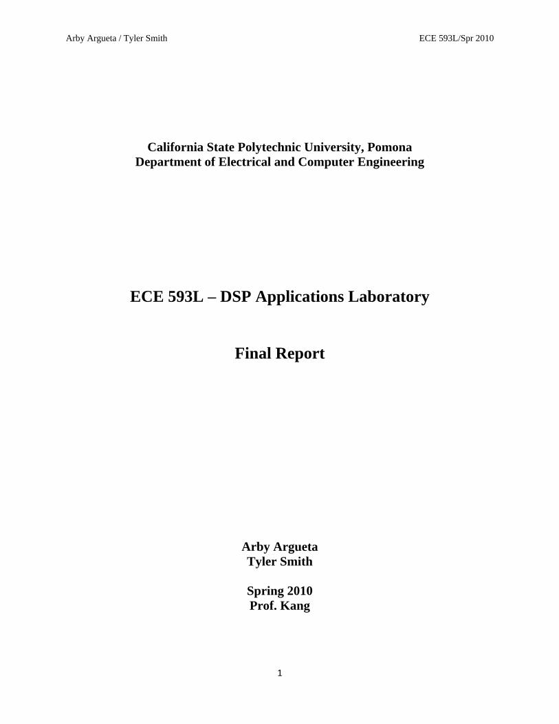
System Overview
The system we are designing in this lab is a basic signal processing block consisting of a
Spartan 3E as the basis of signal processing. The FPGA will be used to create different ways in
which to process the input. This includes creating an AM modulator, double side band
suppressed carrier and other processing systems. The system also consists of three voltage
regulators that output 3.3V, +5V, and -5V that provide power to the system DAC, ADC, and
THS4131. The analog input of the system is first converted to a differential signal through the
THS4131 and is then converted into a digital signal through the ADS8422. The FPGA then
processes the signal in accordance to what it has been programmed to do. The digital output is
then converted into an analog signal using the DAC882 and two opa37 op amps. The analog
output is the processed signal that has processed using the FPGA. There is some accuracy loss
due to the conversion from digital to analog and only having 2^16 values. The different systems
that will be used will be created using Simulink’s Xilinx generator. This program allows us to
created several different systems graphically and have them implemented in hardware. This
gives us the advantage to verify the system before implementing it on the board allows for
greater adaptability. This method also reduces our control over optimization of the system and to
an extent, creates a black box way of generating systems. The program though allows us to
create complex systems quickly that perform the necessary tasks, and are easily altered in
Simulink.
THS4131 ADS8422
DAC8822
Including opa37 opamp
Spartan 3E
FPGAVoltage
Regulators
16 digital lines
Analog Output
16 digita
l lines
Differential
Output
Po
we
r
3.3 5 -5
Po
we
r
5 -5
Analog Input
Clock
Clock
Po
we
r
3.3 5 -5
Arby Argueta / Tyler Smith ECE 593L/Spr 2010
3
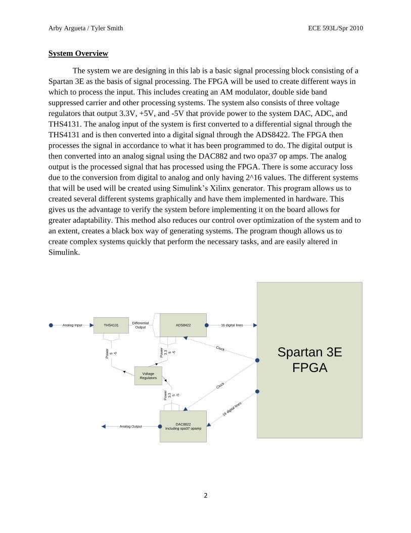
System Design
To implement our system design, we created a circuit design to integrate the various subsystems:
Fully Differential Amplifier (THS4131), Voltage Regulators (+5, -5, +3.3), Analog to Digital
Converter (ADS8422), Digital to Analog Converter(DAC8822), and Op-Amps (OPA37) on a
single pc board. We created this circuit design using PCB123 by Sunmicro.
Our PCB Circuit Design
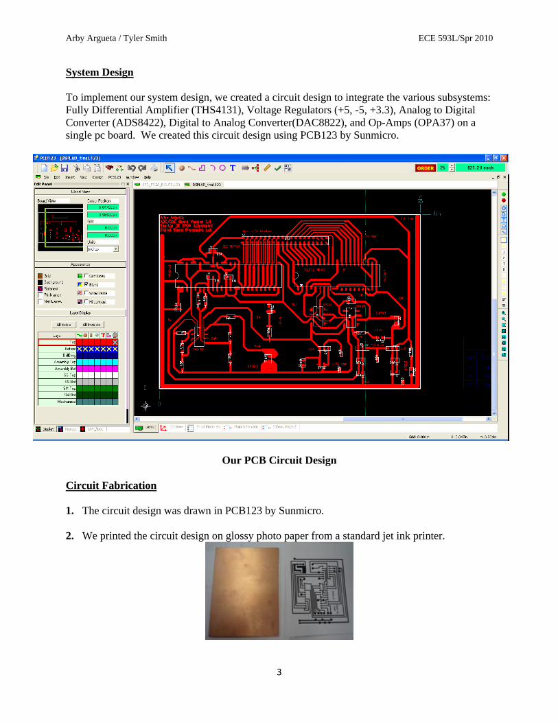
Circuit Fabrication
1. The circuit design was drawn in PCB123 by Sunmicro.
2. We printed the circuit design on glossy photo paper from a standard jet ink printer.

Arby Argueta / Tyler Smith ECE 593L/Spr 2010
4
3. We ironed the design onto a piece of copper for about 20 minutes so the ink could trace could
bond to the copper.
4. We soak it in water for 20 minutes for the paper to being to dissolve. Then we rub off all the
paper.
5. We used a nail and hammer to make indent for all of the holes.
6. We placed the copper in a tub of chemical for 20 minutes to allow the chemical to eat away
all the exposed copper, just leaving our circuit design.
7. We used a dremel with a 1/32 drill bit to drill all the holes.
Arby Argueta / Tyler Smith ECE 593L/Spr 2010
5
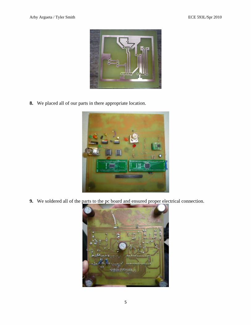
8. We placed all of our parts in there appropriate location.
9. We soldered all of the parts to the pc board and ensured proper electrical connection.
Arby Argueta / Tyler Smith ECE 593L/Spr 2010
6
Subsystem Testing:
Experiment # 2: Fully Differential Amplifier THS4131 and Voltage Regulators
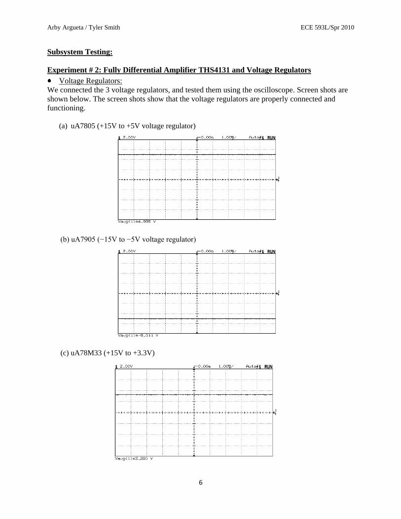
Voltage Regulators:
We connected the 3 voltage regulators, and tested them using the oscilloscope. Screen shots are
shown below. The screen shots show that the voltage regulators are properly connected and
functioning.
(a) uA7805 (+15V to +5V voltage regulator)
(b) uA7905 (−15V to −5V voltage regulator)
(c) uA78M33 (+15V to +3.3V)
Arby Argueta / Tyler Smith ECE 593L/Spr 2010
7
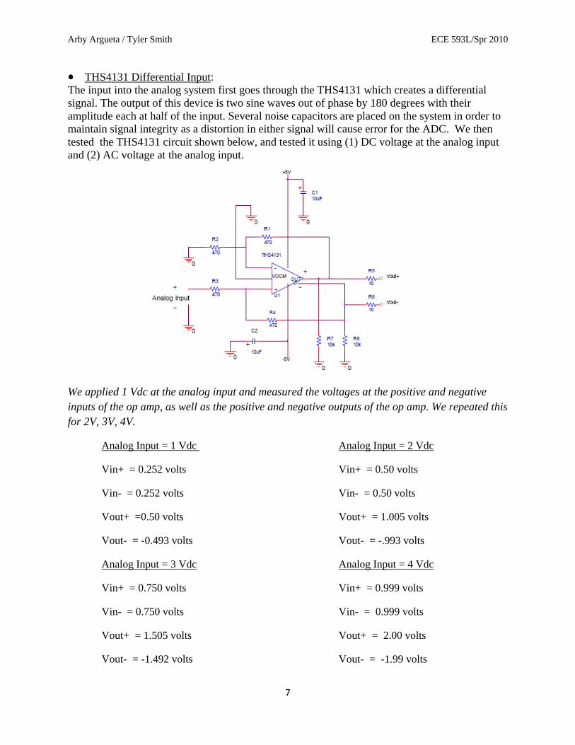
THS4131 Differential Input:
The input into the analog system first goes through the THS4131 which creates a differential
signal. The output of this device is two sine waves out of phase by 180 degrees with their
amplitude each at half of the input. Several noise capacitors are placed on the system in order to
maintain signal integrity as a distortion in either signal will cause error for the ADC. We then
tested the THS4131 circuit shown below, and tested it using (1) DC voltage at the analog input
and (2) AC voltage at the analog input.
We applied 1 Vdc at the analog input and measured the voltages at the positive and negative
inputs of the op amp, as well as the positive and negative outputs of the op amp. We repeated this
for 2V, 3V, 4V.
Analog Input = 1 Vdc Analog Input = 2 Vdc
Vin+ = 0.252 volts Vin+ = 0.50 volts
Vin- = 0.252 volts Vin- = 0.50 volts
Vout+ =0.50 volts Vout+ = 1.005 volts
Vout- = -0.493 volts Vout- = -.993 volts
Analog Input = 3 Vdc Analog Input = 4 Vdc
Vin+ = 0.750 volts Vin+ = 0.999 volts
Vin- = 0.750 volts Vin- = 0.999 volts
Vout+ = 1.505 volts Vout+ = 2.00 volts
Vout- = -1.492 volts Vout- = -1.99 volts
Arby Argueta / Tyler Smith ECE 593L/Spr 2010
8
Experiment # 2 (Continued)
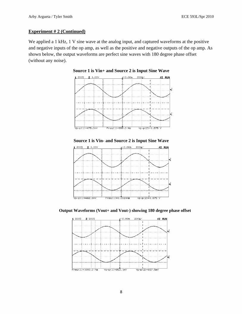
We applied a 1 kHz, 1 V sine wave at the analog input, and captured waveforms at the positive
and negative inputs of the op amp, as well as the positive and negative outputs of the op amp. As
shown below, the output waveforms are perfect sine waves with 180 degree phase offset
(without any noise).
Source 1 is Vin+ and Source 2 is Input Sine Wave
Source 1 is Vin- and Source 2 is Input Sine Wave
Output Waveforms (Vout+ and Vout-) showing 180 degree phase offset
Arby Argueta / Tyler Smith ECE 593L/Spr 2010
9
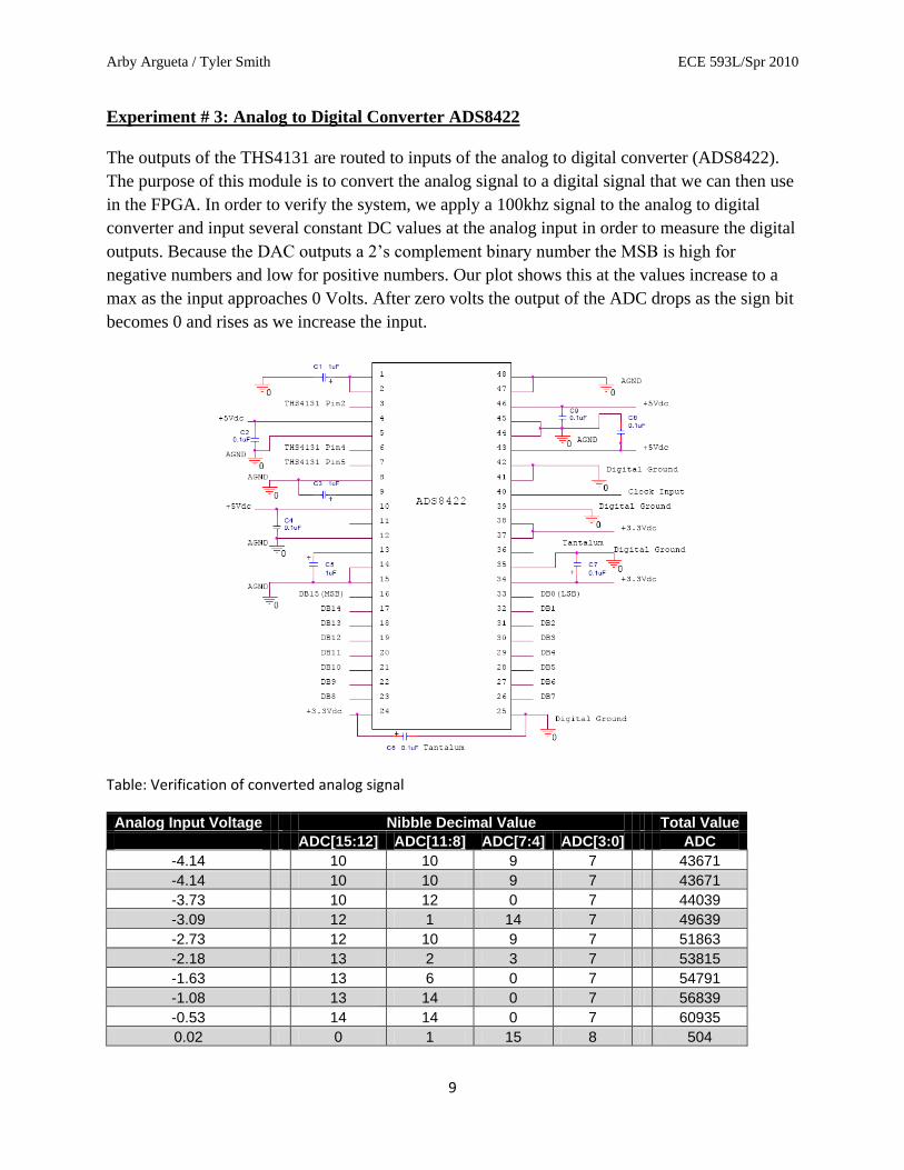
Experiment # 3: Analog to Digital Converter ADS8422
The outputs of the THS4131 are routed to inputs of the analog to digital converter (ADS8422).
The purpose of this module is to convert the analog signal to a digital signal that we can then use
in the FPGA. In order to verify the system, we apply a 100khz signal to the analog to digital
converter and input several constant DC values at the analog input in order to measure the digital
outputs. Because the DAC outputs a 2’s complement binary number the MSB is high for
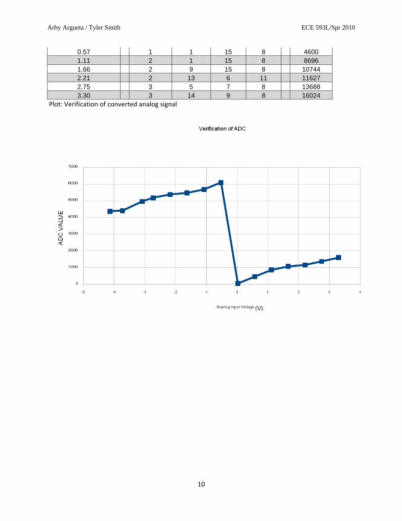
negative numbers and low for positive numbers. Our plot shows this at the values increase to a
max as the input approaches 0 Volts. After zero volts the output of the ADC drops as the sign bit
becomes 0 and rises as we increase the input.
Table: Verification of converted analog signal
Analog Input Voltage Nibble Decimal Value Total Value
ADC[15:12] ADC[11:8] ADC[7:4] ADC[3:0] ADC
-4.14 10 10 9 7 43671
-4.14 10 10 9 7 43671
-3.73 10 12 0 7 44039
-3.09 12 1 14 7 49639
-2.73 12 10 9 7 51863
-2.18 13 2 3 7 53815
-1.63 13 6 0 7 54791
-1.08 13 14 0 7 56839
-0.53 14 14 0 7 60935
0.02 0 1 15 8 504
Arby Argueta / Tyler Smith ECE 593L/Spr 2010
10
0.57 1 1 15 8 4600
1.11 2 1 15 8 8696
1.66 2 9 15 8 10744
2.21 2 13 6 11 11627
2.75 3 5 7 8 13688
3.30 3 14 9 8 16024
Plot: Verification of converted analog signal
Arby Argueta / Tyler Smith ECE 593L/Spr 2010
11
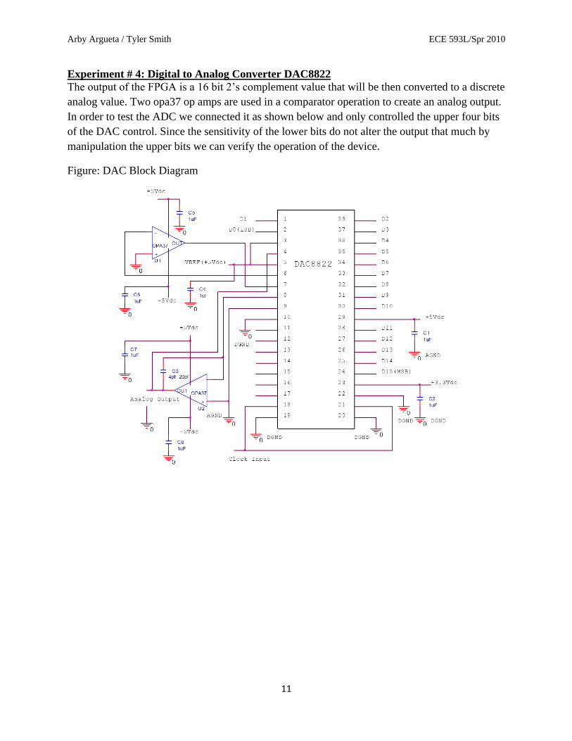
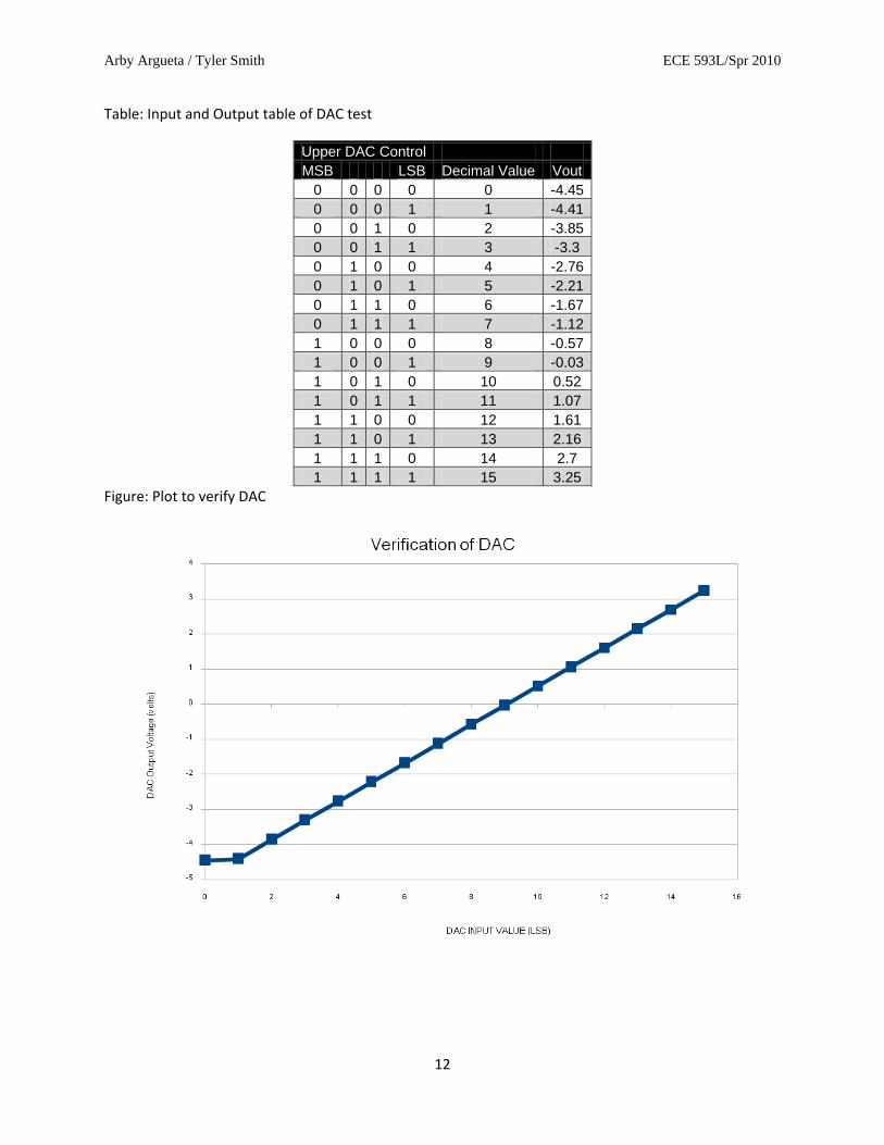
Experiment # 4: Digital to Analog Converter DAC8822
The output of the FPGA is a 16 bit 2’s complement value that will be then converted to a discrete
analog value. Two opa37 op amps are used in a comparator operation to create an analog output.
In order to test the ADC we connected it as shown below and only controlled the upper four bits
of the DAC control. Since the sensitivity of the lower bits do not alter the output that much by
manipulation the upper bits we can verify the operation of the device.
Figure: DAC Block Diagram
Arby Argueta / Tyler Smith ECE 593L/Spr 2010
12
Table: Input and Output table of DAC test
Upper DAC Control
MSB LSB Decimal Value Vout
0 0 0 0 0 -4.45
0 0 0 1 1 -4.41
0 0 1 0 2 -3.85
0 0 1 1 3 -3.3
0 1 0 0 4 -2.76
0 1 0 1 5 -2.21
0 1 1 0 6 -1.67
0 1 1 1 7 -1.12
1 0 0 0 8 -0.57
1 0 0 1 9 -0.03
1 0 1 0 10 0.52
1 0 1 1 11 1.07
1 1 0 0 12 1.61
1 1 0 1 13 2.16
1 1 1 0 14 2.7
1 1 1 1 15 3.25
Figure: Plot to verify DAC
Arby Argueta / Tyler Smith ECE 593L/Spr 2010
13
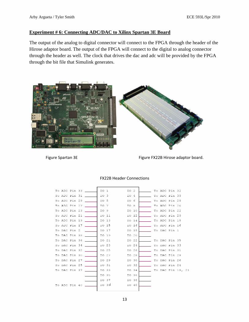
Experiment # 6: Connecting ADC/DAC to Xilinx Spartan 3E Board
The output of the analog to digital connector will connect to the FPGA through the header of the
Hirose adaptor board. The output of the FPGA will connect to the digital to analog connector
through the header as well. The clock that drives the dac and adc will be provided by the FPGA
through the bit file that Simulink generates.
Figure Spartan 3E Figure FX22B Hirose adaptor board.
FX22B Header Connections
Arby Argueta / Tyler Smith ECE 593L/Spr 2010
14
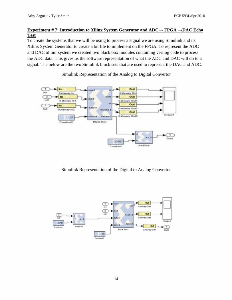
Experiment # 7: Introduction to Xilinx System Generator and ADC→ FPGA →DAC Echo
Test
To create the systems that we will be using to process a signal we are using Simulink and its
Xilinx System Generator to create a bit file to implement on the FPGA. To represent the ADC
and DAC of our system we created two black box modules containing verilog code to process
the ADC data. This gives us the software representation of what the ADC and DAC will do to a
signal. The below are the two Simulink block sets that are used to represent the DAC and ADC.
Simulink Representation of the Analog to Digital Convertor
Simulink Representation of the Digital to Analog Convertor
Arby Argueta / Tyler Smith ECE 593L/Spr 2010
15
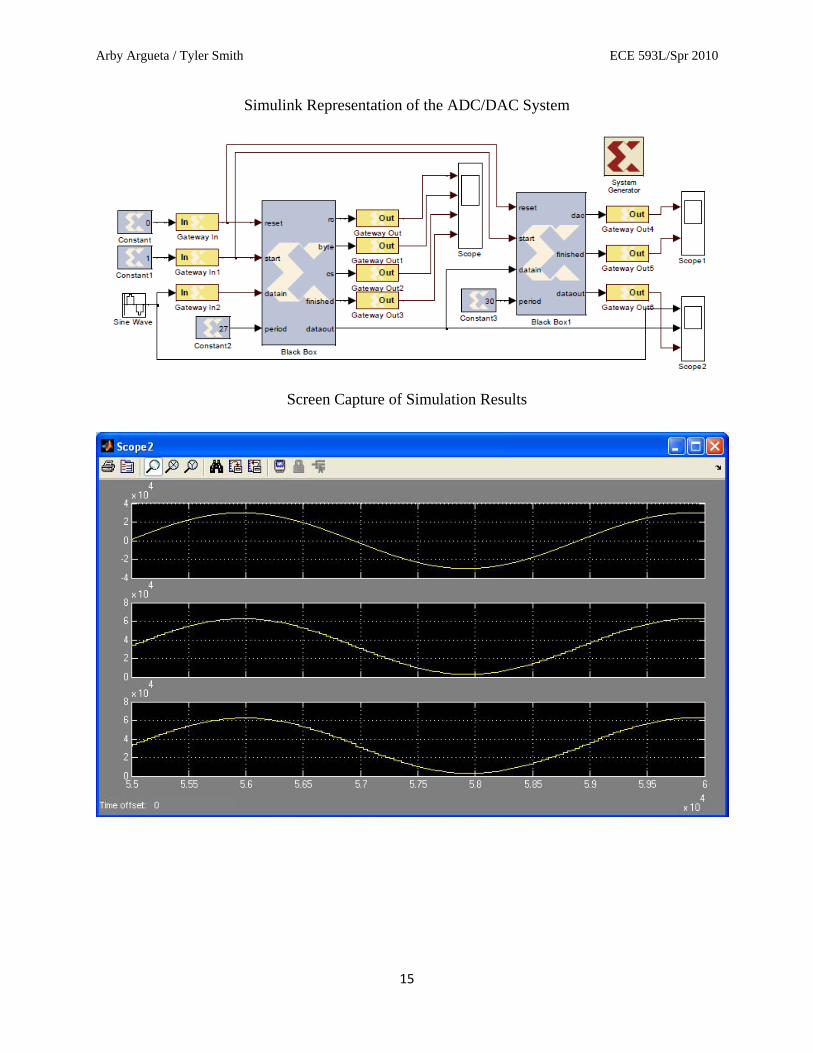
Simulink Representation of the ADC/DAC System
Screen Capture of Simulation Results
Arby Argueta / Tyler Smith ECE 593L/Spr 2010
16
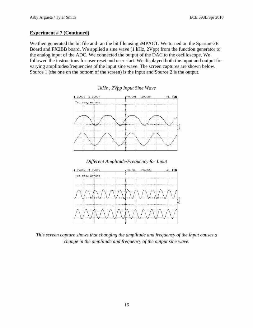
Experiment # 7 (Continued)
We then generated the bit file and ran the bit file using iMPACT. We turned on the Spartan-3E
Board and FX2BB board. We applied a sine wave (1 kHz, 2Vpp) from the function generator to
the analog input of the ADC. We connected the output of the DAC to the oscilloscope. We
followed the instructions for user reset and user start. We displayed both the input and output for
varying amplitudes/frequencies of the input sine wave. The screen captures are shown below.
Source 1 (the one on the bottom of the screen) is the input and Source 2 is the output.
1kHz , 2Vpp Input Sine Wave
Different Amplitude/Frequency for Input
This screen capture shows that changing the amplitude and frequency of the input causes a
change in the amplitude and frequency of the output sine wave.
Arby Argueta / Tyler Smith ECE 593L/Spr 2010
17
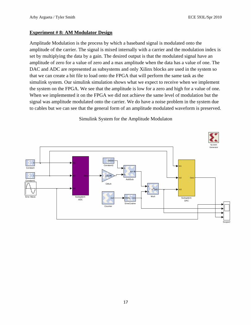
Experiment # 8: AM Modulator Design
Amplitude Modulation is the process by which a baseband signal is modulated onto the
amplitude of the carrier. The signal is mixed internally with a carrier and the modulation index is
set by multiplying the data by a gain. The desired output is that the modulated signal have an
amplitude of zero for a value of zero and a max amplitude when the data has a value of one. The
DAC and ADC are represented as subsystems and only Xilinx blocks are used in the system so
that we can create a bit file to load onto the FPGA that will perform the same task as the
simulink system. Our simulink simulation shows what we expect to receive when we implement
the system on the FPGA. We see that the amplitude is low for a zero and high for a value of one.
When we implemented it on the FPGA we did not achieve the same level of modulation but the
signal was amplitude modulated onto the carrier. We do have a noise problem in the system due
to cables but we can see that the general form of an amplitude modulated waveform is preserved.
Simulink System for the Amplitude Modulaton
In1
In2
In3
Out1
Subsystem
DAC
In1
In2
In3
Out1
Subsystem
ADCsysgentheta cos
SineCosine
Sine Wave
Scope2
sysgen
a
b(ab)z
-3
Multsysgenout
Counter
20000
Constant2
1
Constant1
0
Constant
sysgenx 0.75
CMult
sysgen
a
b
a + b
AddSub
Sy stem
Generator
Arby Argueta / Tyler Smith ECE 593L/Spr 2010
18
Experiment # 8 (Continued)
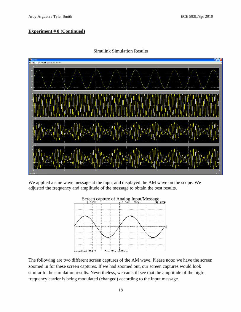
Simulink Simulation Results
We applied a sine wave message at the input and displayed the AM wave on the scope. We
adjusted the frequency and amplitude of the message to obtain the best results.
Screen capture of Analog Input/Message
The following are two different screen captures of the AM wave. Please note: we have the screen
zoomed in for these screen captures. If we had zoomed out, our screen captures would look
similar to the simulation results. Nevertheless, we can still see that the amplitude of the high-
frequency carrier is being modulated (changed) according to the input message.
Arby Argueta / Tyler Smith ECE 593L/Spr 2010
19
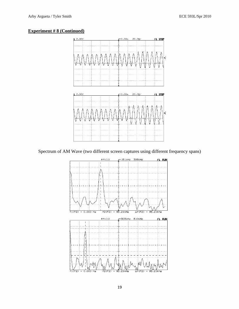
Experiment # 8 (Continued)
Spectrum of AM Wave (two different screen captures using different frequency spans)
Arby Argueta / Tyler Smith ECE 593L/Spr 2010
20
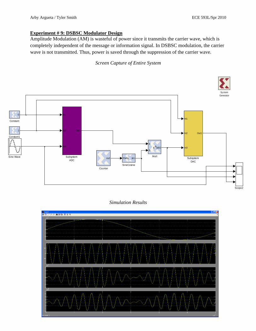
Experiment # 9: DSBSC Modulator Design
Amplitude Modulation (AM) is wasteful of power since it transmits the carrier wave, which is
completely independent of the message or information signal. In DSBSC modulation, the carrier
wave is not transmitted. Thus, power is saved through the suppression of the carrier wave.
Screen Capture of Entire System
Simulation Results
In1
In2
In3
Out1
Subsystem
DAC
In1
In2
In3
Out1
Subsystem
ADCsysgentheta sin
SineCosine
Sine Wave
Scope2
sysgen
a
b(ab)z
-3
Multsysgenout
Counter
1
Constant1
0
Constant
Sy stem
Generator
Arby Argueta / Tyler Smith ECE 593L/Spr 2010
21
Experiment # 9 (Continued)
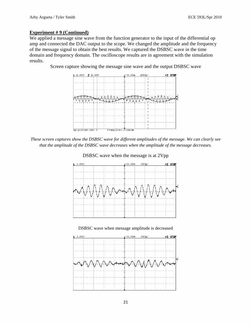
We applied a message sine wave from the function generator to the input of the differential op
amp and connected the DAC output to the scope. We changed the amplitude and the frequency
of the message signal to obtain the best results. We captured the DSBSC wave in the time
domain and frequency domain. The oscilloscope results are in agreement with the simulation
results.
Screen capture showing the message sine wave and the output DSBSC wave
These screen captures show the DSBSC wave for different amplitudes of the message. We can clearly see
that the amplitude of the DSBSC wave decreases when the amplitude of the message decreases.
DSBSC wave when the message is at 2Vpp
DSBSC wave when message amplitude is decreased
Arby Argueta / Tyler Smith ECE 593L/Spr 2010
22
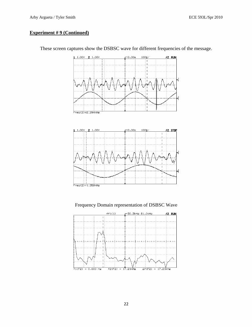
Experiment # 9 (Continued)
These screen captures show the DSBSC wave for different frequencies of the message.
Frequency Domain representation of DSBSC Wave
Arby Argueta / Tyler Smith ECE 593L/Spr 2010
23
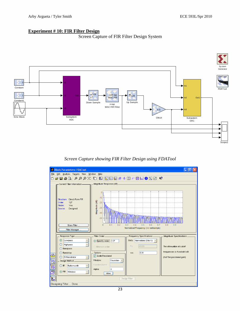
Experiment # 10: FIR Filter Design
Screen Capture of FIR Filter Design System
Screen Capture showing FIR Filter Design using FDATool
128 tap
MAC FIR
n-tap
MAC FIR Filter
sysgen128
Up Sample
In1
In2
In3
Out1
Subsystem
DAC
In1
In2
In3
Out1
Subsystem
ADC
Sine Wave
Scope2
FDATool
FDATool
sysgen128
z-1
Down Sample
1
Constant1
0
Constant
sysgenx 1
CMult
Sy stem
Generator
Arby Argueta / Tyler Smith ECE 593L/Spr 2010
24
Experiment # 10 (Continued):
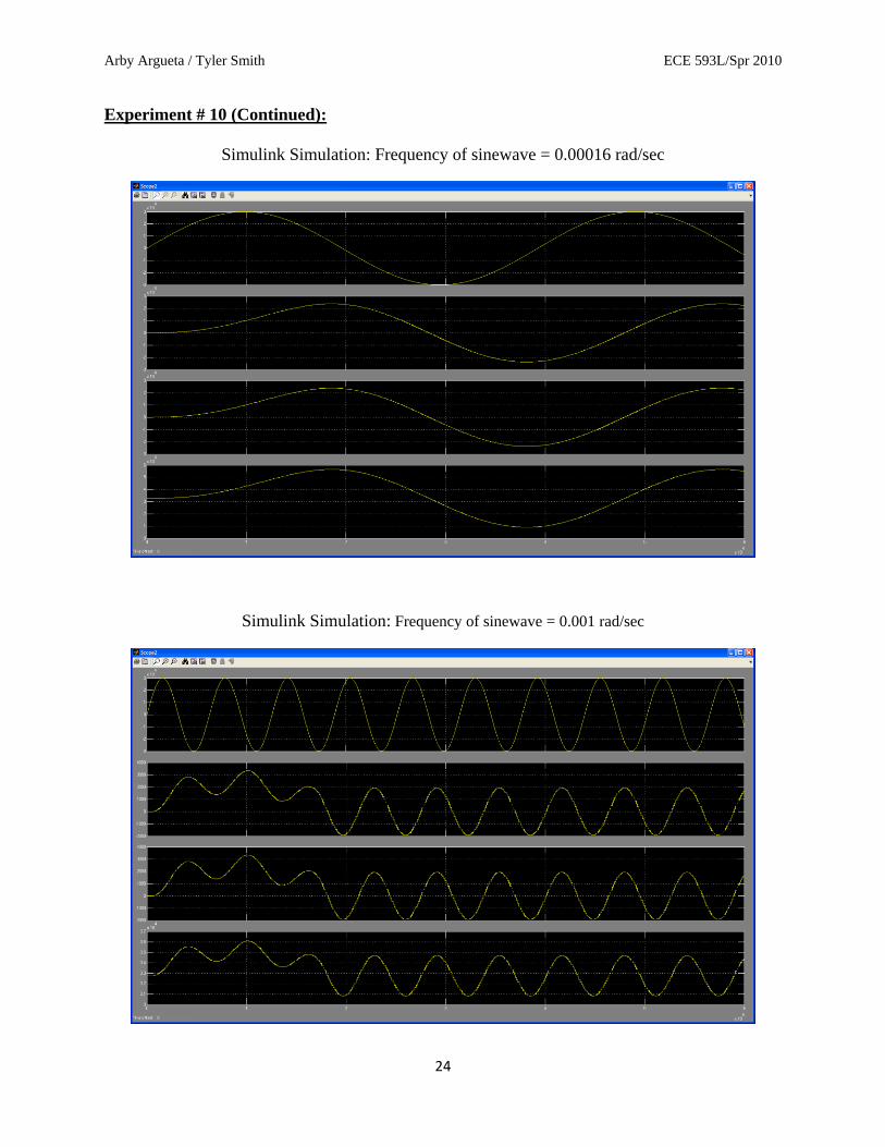
Simulink Simulation: Frequency of sinewave = 0.00016 rad/sec
Simulink Simulation: Frequency of sinewave = 0.001 rad/sec
Arby Argueta / Tyler Smith ECE 593L/Spr 2010
25
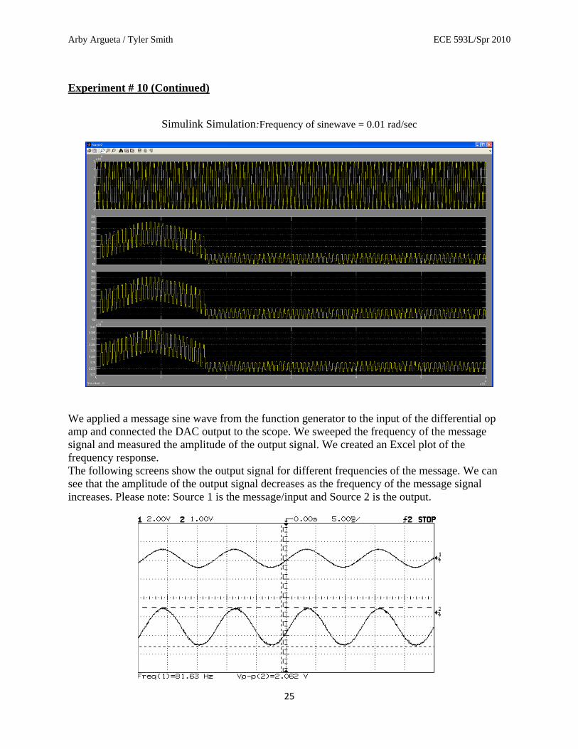
Experiment # 10 (Continued)
Simulink Simulation:Frequency of sinewave = 0.01 rad/sec
We applied a message sine wave from the function generator to the input of the differential op
amp and connected the DAC output to the scope. We sweeped the frequency of the message
signal and measured the amplitude of the output signal. We created an Excel plot of the
frequency response.
The following screens show the output signal for different frequencies of the message. We can
see that the amplitude of the output signal decreases as the frequency of the message signal
increases. Please note: Source 1 is the message/input and Source 2 is the output.
Arby Argueta / Tyler Smith ECE 593L/Spr 2010
26
Experiment # 10 (Continued)
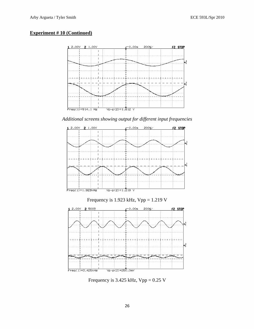
Additional screens showing output for different input frequencies
Frequency is 1.923 kHz, Vpp = 1.219 V
Frequency is 3.425 kHz, Vpp = 0.25 V
Arby Argueta / Tyler Smith ECE 593L/Spr 2010
27
Experiment # 10 (Continued)
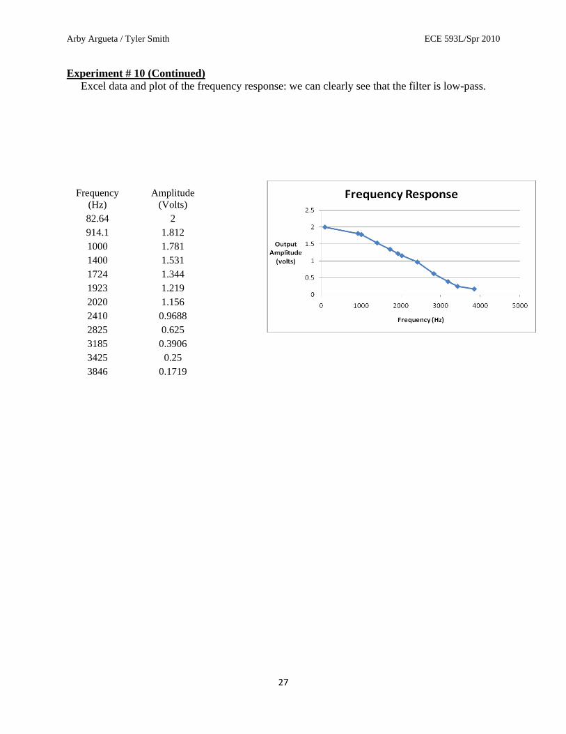
Excel data and plot of the frequency response: we can clearly see that the filter is low-pass.
Frequency
(Hz)
Amplitude
(Volts)
82.64 2
914.1 1.812
1000 1.781
1400 1.531
1724 1.344
1923 1.219
2020 1.156
2410 0.9688
2825 0.625
3185 0.3906
3425 0.25
3846 0.1719
Arby Argueta / Tyler Smith ECE 593L/Spr 2010
28
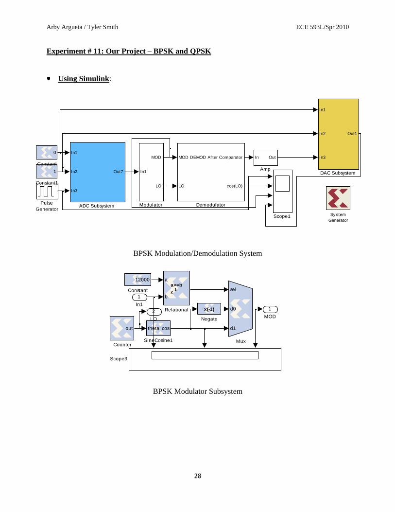
Experiment # 11: Our Project – BPSK and QPSK
Using Simulink:
Scope1
Pulse
Generator
In1
MOD
LO
Modulator
MOD
LO
DEMOD Af ter Comparator
cos(LO)
Demodulator
In1
In2
In3
Out1
DAC Subsystem1
Constant1
0
Constant
In Out
Amp
In1
In2
In3
Out7
ADC Subsystem
Sy stem
Generator
BPSK Modulation/Demodulation System
2
LO
1
MOD
sysgentheta cos
SineCosine1
Scope3
sysgen
a
b
a>=b
z-1
Relational sysgenx(-1)
Negate
sysgen
sel
d0
d1
Mux
sysgenout
Counter
12000
Constant
1
In1
BPSK Modulator Subsystem
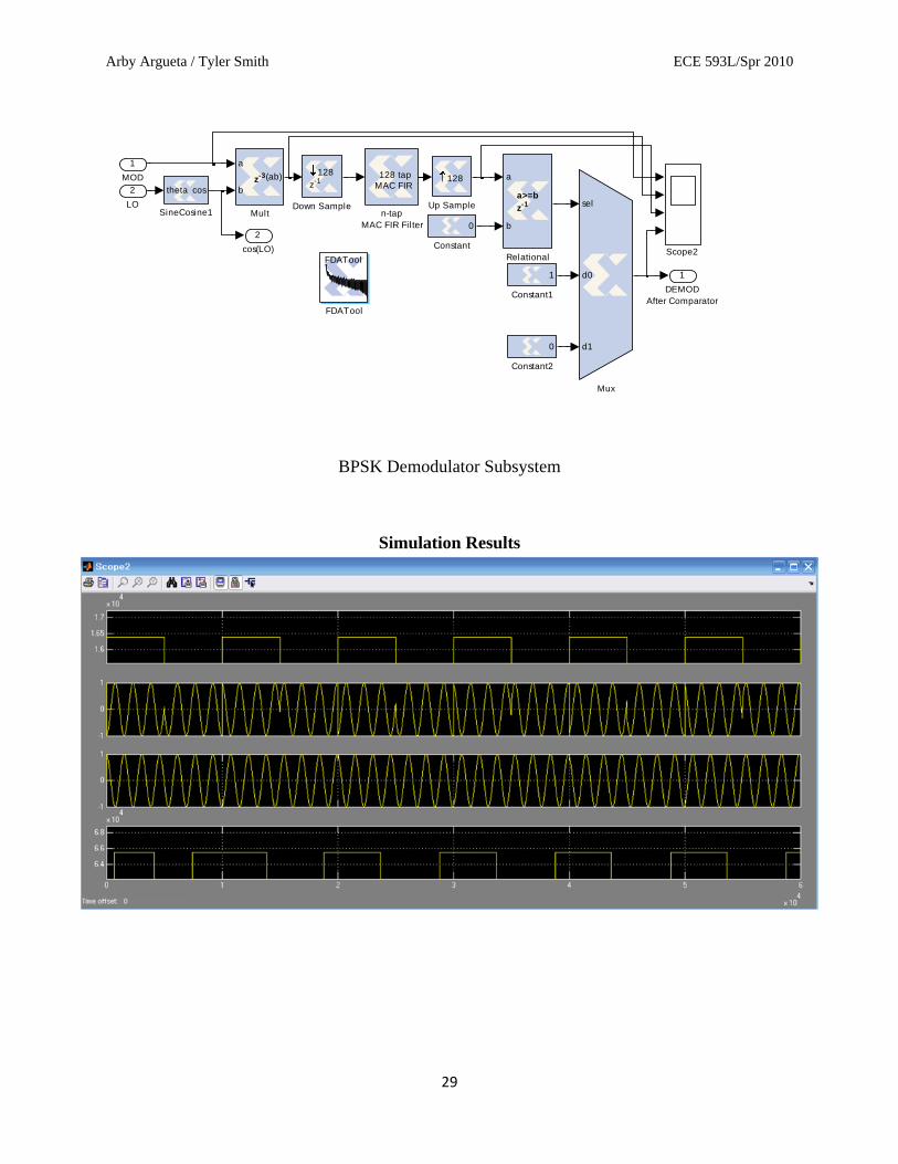
Arby Argueta / Tyler Smith ECE 593L/Spr 2010
29
2
cos(LO)
1
DEMOD
After Comparator
128 tap
MAC FIR
n-tap
MAC FIR Filter
sysgen128
Up Sample
sysgentheta cos
SineCosine1
Scope2
sysgen
a
b
a>=b
z-1
Relational
sysgen
sel
d0
d1
Mux
sysgen
a
b
(ab)z-3
Mult
FDATool
FDATool
sysgen128
z-1
Down Sample
0
Constant2
1
Constant1
0
Constant
2
LO
1
MOD
BPSK Demodulator Subsystem
Simulation Results
Arby Argueta / Tyler Smith ECE 593L/Spr 2010
30
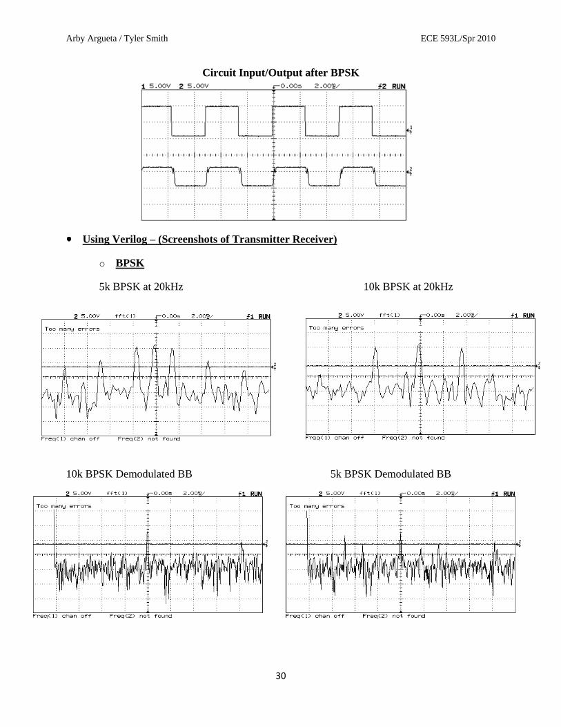
Circuit Input/Output after BPSK
Using Verilog – (Screenshots of Transmitter Receiver)
o BPSK
5k BPSK at 20kHz 10k BPSK at 20kHz
10k BPSK Demodulated BB 5k BPSK Demodulated BB
Arby Argueta / Tyler Smith ECE 593L/Spr 2010
31
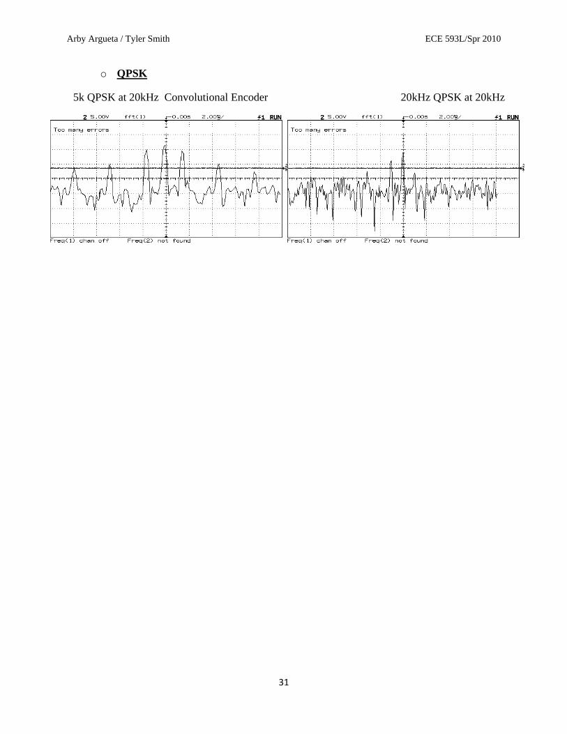
o QPSK
5k QPSK at 20kHz Convolutional Encoder 20kHz QPSK at 20kHz


![Ece-Vii-dsp Algorithms & Architecture [10ec751]-Notes](https://img.pdfslide.net/doc/110x75/5695d4481a28ab9b02a0ea8e/ece-vii-dsp-algorithms-architecture-10ec751-notes.jpg)