Embed Size (px)
Citation preview

High Speed Analog Design and Application Seminar
3-1Texas Instruments
Section 3
Useful Things to Know aboutHigh-Speed A/D Converters
High Speed Analog Design and Application Seminar
3-2Texas Instruments
Agenda
Understanding the ADC InputWorking with the ADC InputADC ReferencesClock ConsiderationsADC’s Digital Data Outputs
Appendix:• HS-ADC Testing
- Bench Test Setup and Equipment
• Pipeline Architecture, Basic Overview
Today’s High-Speed A/D converter feature a wide dynamic range at very highsampling rates. In order to preserve and utilize this wide dynamic range, carefulattention must be given to the details of applying the A/D converter. The designerwill find a lot of useful application information and circuit suggestions in theproduct data sheets. While the datasheets focus on model specific information,however, it typically does not go into the details that would help particularly theinexperienced designer to gain a fundamental understanding of high-speed A/Dconverter. This section of the seminar is designed to review some of the relevantfundamentals in and around High-Speed Pipeline ADCs.

High Speed Analog Design and Application Seminar
3-3Texas Instruments
High-Speed A/D Converter
Sampling rate, Fs >10MspsAlmost always ‘Pipeline’ ADCsMonolithic CMOS DevicesSingle-Supply (analog, digital)Integrated S&H -> ADSInternal ReferenceLow-Voltage, Single-Ended Logic Outputs(LVCMOS, typ. +3.3V, +1.8V)Emphasis on Dynamic Performance
The term ‘High-Speed’ can be found in combination with a lot of different productlines. For this presentation it is used for A/D converter with a sampling or clockrate of more than 10Msps. Such converter are in most cases based on the‘pipeline’ architecture (see Appendix for more details on the principals of PipelineADCs), and fabricated using a sub-micron CMOS process. Some convertermodel designed for very-low power consumption operate on only 1.8V supplies, aresult of a 0.18um process used. Most such ADCs are single-supply components,which poses certain restrictions on their operating conditions, a topic that will belooked at throughout this presentation. Based on switched capacitor techniques,High-Speed ADCs typically have a build-in Sample&Hold circuit, as well asinternal references. The use of external reference is in most cases an availableoption. The supplies of the converter is usually such that it provides a dedicatedoutput driver supply pin. This allows the digital outputs to be interfaced to avariety of logic families. Most High-Speed A/D converter are designed to achievea certain, high level of dynamic performance, i.e. in terms of SFDR and SNR. Itshould be noted that in order to meet those ac-performances dc accuracy istypically compromised. For example, gain and offset error are often in the percentrange.

High Speed Analog Design and Application Seminar
3-4Texas Instruments
Understanding the ADC Input
High Speed Analog Design and Application Seminar
3-5Texas Instruments
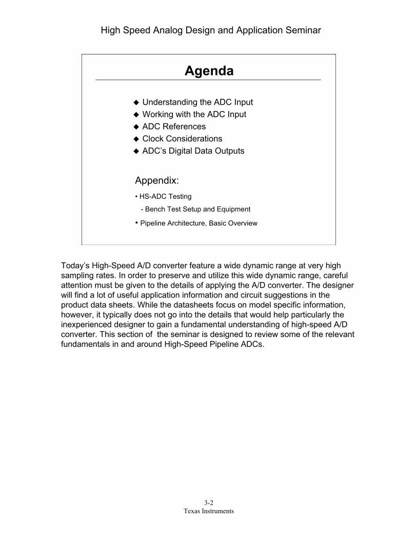
Understanding the ADC InputWhat’s the nature of the inputs?
Differential InputsLooking into a S&HSwitched Cap InputsDynamic Input ImpedanceEffectively ‘Capacitive’ Load
What are the ac and dc constraints?Full-Scale Input Range (FSR in Vp-p)DC-Input Common-mode Voltage (VCM)Analog Input Bandwidth
IN
IN
ADC
+Vs
Typically, a particular high-speed ADC model is selected based on its sampling speed anddynamic performance at certain frequencies or over a bandwidth of interest. For the systemdesigner this selection process is not always easy. Often the system requirements are uniqueand the relevant information can not directly be extracted from the product datasheetExtrapolating the achievable performance bears some risk and to minimize the possible errorsources the designer must pay careful attention to the issue of the ‘interface’. Theconsiderations on the interface include an understanding of the input of the ADC – what effectit will have on the driving source and it’s constraints.
The signal inputs to the ADC are typically differential, which has a number of advantages, andwill be discussed throughout the presentations. What the driving source sees is the input stageSample&Hold amplifier, who’s architecture employs switched capacitors. Here, switches aretypically connected directly to the input pins and switching transients occur as a function of theclock. Consequently, the input impedance is neither constant nor just resistive, but dynamicand highly capacitive in nature.
The full-scale input range of the ADC is usually determined by the internal references. Notethat there will be a significant difference in the required signal amplitude between differentialand single-ended input configurations; typically a factor of two. In either case, most high-speedADCs require their inputs to be biased up to a defined common-mode voltage. It is usuallyaround half the supply voltage, and can be adjusted within a range without too much trade-offin performance.
One other consideration that comes into play particularly for undersampling or IF-samplingapplications is the ‘Analog Input Bandwidth’ of the ADC.

High Speed Analog Design and Application Seminar
3-6Texas Instruments
Interfacing the input signal differentially to the high-speed ADCs is usually therecommended configuration as it leads to the highest achievable dynamicperformance. Most ADCs are specified based on the differential input configuration.
Compared to single-ended, differential inputs require two signals that are180degrees out of phase, but each of the two signal requires only half the signalamplitude. This is essential as it typically translates into reduced distortion from thedriving source. Differential signaling also leads to a significant reduction in even-order harmonics. This is desirable since the second harmonic is often dominant andhigher order harmonics can be filtered more easily. Furthermore, common-modenoise can be greatly suppressed.
Most high-speed ADCs designed for 3V to 5V power supplies operate with a full-scale input range of about 2Vp-p. This typically represents a good compromisebetween the achievable signal-to-noise ratio (SNR), and the distortion performance(THD, SFDR). Depending on the application, optimizations towards one or the othercan be made, but will also affect the requirements for the driver circuit.
ADC – Differential Input
Differential/Complementary InputsTwo Input Signals, Complementary½ Signal Swing compared to SEReduces Even-Order Harmonics, compared to SEImproves Common-Mode Noise RejectionFull-Scale Input Range:
• Typically 2Vp-p span for best Distortion and Noisetrade-off
• Can include Rail-to-Rail Operation
Directly Affects Requirements for Driver Circuit
High Speed Analog Design and Application Seminar
3-7Texas Instruments
Single-ended vs. Differential Signals
GND
VDiff (p-p)
Vp+
VCM
Vp-
IN
IN
A/D
2. Driving Differential Inputs Differentially +Vs
GND
More headroom
VDiff (p-p)IN
IN
1. Driving Differential Inputs Single-Ended
A/DVSE (p-p)
+VsLittle headroom
VCM
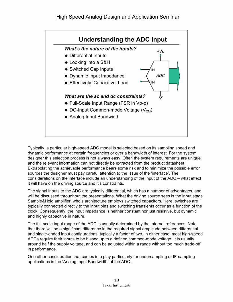
This slide shows the difference in required input signal amplitude between thesingle-ended input configuration and the differential input configuration. It alsoshows very clearly that for a given supply rail (+Vs) the differential signalingapproach leaves significantly more headroom – the distance between the peaksignal amplitude and the supply rail. Typically, as the signal amplitudeapproaches the supply rail distortion from the driving source, as well as the ADC,increases.

High Speed Analog Design and Application Seminar
3-8Texas Instruments
Single-ended vs. DifferentialInterface Tradeoffs
Single-ended InputsDegraded dynamic performance (larger FSR)Common-mode voltage and op amp headroom maylimit use for dc-couplingMay be best suited for Time Domain application
DifferentialOptimized performance due to lower FSR, Reductionof even-order and common-mode componentsBest for higher input frequencies (IFs)More complex driver circuitry
This slide summarizes the key points between a single-ended and differential interface.Even though the single-ended configuration has a number of draw backs it is still a viableoption for time domain based applications. For example, for a CCD imaging system theemphasis is clearly on maximizing the signal-to-noise ratio and the increase in distortionthat may result can be accepted. A related point is whether or not the system requires dc-or ac-coupling. Here, dc-coupling often places additional constraints on the interfacecircuit implementation.
For almost all high-speed A/D converter it can be said that in most applications, using thedifferential input configuration along with ac-coupling results in the best obtainable ADCperformance.
Some general observations:
The distortion and SFDR performance typically improves with smaller signal amplitudes.
The SNR performance typically improves with larger signal amplitudes.
The distortion and SFDR performance typically degrades as the input frequency increases.
The SNR typically degrades as well with higher input frequencies. This is often primarilydue to jitter having a higher impact. See the discussion on clock and jitter later in thispresentation.
High Speed Analog Design and Application Seminar
3-9Texas Instruments
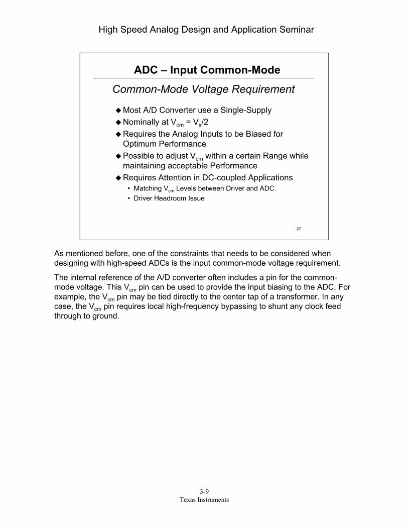
As mentioned before, one of the constraints that needs to be considered whendesigning with high-speed ADCs is the input common-mode voltage requirement.
The internal reference of the A/D converter often includes a pin for the common-mode voltage. This Vcm pin can be used to provide the input biasing to the ADC. Forexample, the Vcm pin may be tied directly to the center tap of a transformer. In anycase, the Vcm pin requires local high-frequency bypassing to shunt any clock feedthrough to ground.
ADC – Input Common-Mode
Common-Mode Voltage Requirement
Most A/D Converter use a Single-SupplyNominally at Vcm = Vs/2Requires the Analog Inputs to be Biased forOptimum PerformancePossible to adjust Vcm within a certain Range whilemaintaining acceptable PerformanceRequires Attention in DC-coupled Applications
• Matching Vcm Levels between Driver and ADC• Driver Headroom Issue
27

High Speed Analog Design and Application Seminar
3-10Texas Instruments
AC Performance vs Common-Mode Voltage
Example of an ADC’s AC Performance over a range ofInput Common-Mode Voltage
50.0
60.0
70.0
80.0
90.0
0.25 0.75 1.25 1.75 2.25
Common Mode (V)
(dB
FS)
SFDR SNR

High Speed Analog Design and Application Seminar
3-11Texas Instruments
Analog Input Sample & Hold Amplifier Circuit
The sample and hold amplifier is implemented using switched cap techniques. Asimplified functional block diagram is shown here. The SHA is in sample modewhen the clock is high and in hold mode when it is low. In sample mode the F 1switches are closed and the differential input signal is sampled onto thecapacitors Cs. As the CLK falling edge occurs, the F 1 switches are opened andthe SHA is now placed into hold mode. The F 2 switches are subsequently closed,and the voltage across the sampling capacitors is then transferred to the output ofthe S/H amplifier.
ADC Simplified Input Circuit
ø1 ø1ø2
Input Clock
Internal Clock, non-overlapping
tCONVø1
ø2
ø1
ø1
ø1
Out
OutIN
IN
CSVCMi
CSVCMi
ø2
VCMi = internal common-mode voltage
Differential Sample & Hold (Flip-around)

High Speed Analog Design and Application Seminar
3-12Texas Instruments
Because the input to the sample and hold amplifier is a switched capacitor circuit, the inputimpedance is dynamic and dependent upon the sampling rate of the converter. The effectiveresistance of the dynamic load for each input is defined by the following equation.
Input Impedance: Zin = 1 / (Fs * Cs )
Where Cs = Sampling Capacitor; Fs = Sampling clock frequency in Hz; Ron = ON resistance ofMOS switch
Zin : - High Static (no clock) Input Impedance, >1Mohm
- Dynamic Input Impedance Proportional to Sampling Clock
Small sampling capacitor values allow for very fast charging times, which corresponds to fastacquisition times. However, the trade-off here is the noise. The generated switching inducednoise is equivalent to en= √kT/Cs. It can easily be seen that reducing the sampling capacitorvalue is reciprocally affecting the noise.
The components Ron and Cs also determine the ADCs ‘Analog Input Bandwidth’, a topic that willbe discussed later in this seminar.
The time averaged charging of the sampling capacitor will cause a net dc current to flow into theADC’s input. The magnitude of this current changes depending on the clock frequency. Current(Iin) inrush to charge Cs to Vin. Q = Cs * (Vin – Vcm)
The implementation of this transmission gate type switch typically includes the use of‘bootstrapping’. The purpose is to maintain a constant VGS on the transistors and linearize thevoltage dependency of the on resistance. This will help minimizing the distortion generated. Thisis particularly critical for IF sampling applications. Another advantage is that the ADC’sperformance becomes less sensitive to the external common-mode voltage.
ADC Input - Switched Capacitor
ø1CLKH
ø2CLKLVIN
CS
VCM
(ParasiticCapacitance)
CP
ZIN
IINRON
1Cfc
RZs
ONIN +=
ADC
1Cfc
Rs
ON <<
Typically:
Example: Cs = 5pF Zin ~ 2000Ω @ 100MspsZin ~ 20kΩ @10Msps
Load to the driving Source !
Equivalent Input Impedance:

High Speed Analog Design and Application Seminar
3-13Texas Instruments
During the sampling phase (typically half the clock period) the driving source mustcharge or discharge the sampling capacitors to the new value. The conditionencountered by the driver is a rapid change of its load and it must recover from thistransient and settle to the new value. The worst case would be a full-scale excursion,but in most cases the input slew rate is significantly less. But even in this case theinstantaneous demand of charging current could be challenging for a driver, e.g. anop amp, especially since the signal should be settled to within ½ LSB.Unsymmetrical or incomplete settling will result in an increase in distortion andreduction in the achievable SFDR performance. Ideally, the source impedance seenby the inputs of the high-speed ADC should be low and constant over a widebandwidth.
Most ADC input driver configurations benefit from adding low value series resistorsat the inputs of the ADC as well as shunt capacitors. Those simple components canbe instrumental in achieving the listed requirements.
Driving the ADC Input
Driver must charge or discharge ADC sampling cap tothe new input voltageSettle to ½LSB in the sample period of fs/2Differential Inputs require Symmetrical SettlingIncomplete Settling may degrade SFDR performanceSource Impedance looking back from the ADC shouldbe low up to high frequencies
Input Driver Requirements

High Speed Analog Design and Application Seminar
3-14Texas Instruments
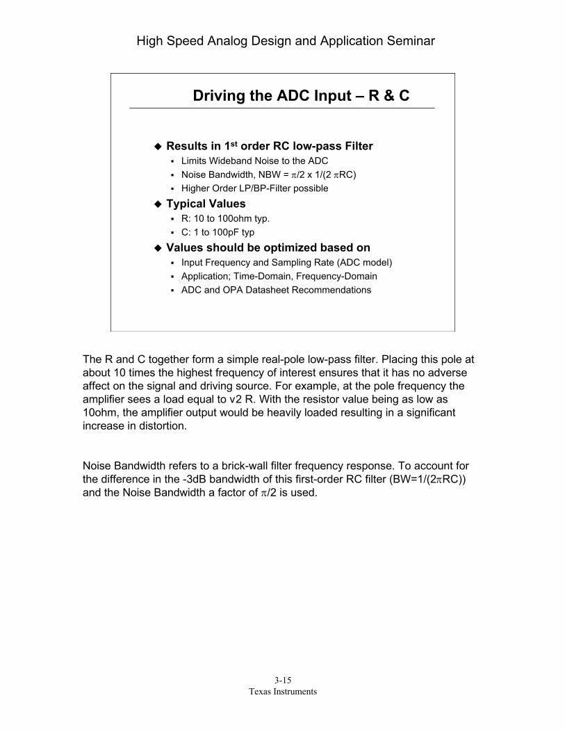
This slide describes the use and functions of the series resistors, R, and the shuntcapacitors ,C. References to the resistors and capacitors as shown here can befound in most product datasheets as a means to optimize the performance of inputdriver configuration for pipeline ADC. While the values may be different their use istypically recommended for transformer based as well as amplifier based circuits.
Driving the ADC Input – R & C
Insert Series Resistor, RReduces peak transient currentDecouples driver from capacitive ADC input(improves settling time due to reduced ringing)
Add Shunt Capacitor, CSupplies/absorbs charge from internal Cs duringsampling phaseShunts switching related current transients to ground
Cs S/H
R
RC
C
IN
IN
Optimizing Driver Performance
High Speed Analog Design and Application Seminar
3-15Texas Instruments
Driving the ADC Input – R & C
Results in 1st order RC low-pass FilterLimits Wideband Noise to the ADCNoise Bandwidth, NBW = π/2 x 1/(2 πRC)Higher Order LP/BP-Filter possible
Typical ValuesR: 10 to 100ohm typ.C: 1 to 100pF typ
Values should be optimized based onInput Frequency and Sampling Rate (ADC model)Application; Time-Domain, Frequency-DomainADC and OPA Datasheet Recommendations
The R and C together form a simple real-pole low-pass filter. Placing this pole atabout 10 times the highest frequency of interest ensures that it has no adverseaffect on the signal and driving source. For example, at the pole frequency theamplifier sees a load equal to v2 R. With the resistor value being as low as10ohm, the amplifier output would be heavily loaded resulting in a significantincrease in distortion.
Noise Bandwidth refers to a brick-wall filter frequency response. To account forthe difference in the -3dB bandwidth of this first-order RC filter (BW=1/(2πRC))and the Noise Bandwidth a factor of π/2 is used.

High Speed Analog Design and Application Seminar
3-16Texas Instruments
Optimizing the ADC Interface
Observations:Increasing R and/or C
improves SNR, due to lower f –3dB point of RC-LPreduces SFDR, due to longer settling time
Note:R’s have 1% tolerance typ.C’s have 10% tolerance typ.
SNR SFDR
Trying to optimize the interface circuit including the adjustments of the R and Cvalues the designer should be aware of their effects and the resulting constraints.Generally, the values can only be changed within a certain range before theADC’s performance is negatively impacted. Also, choosing component valuesthat seem to improve the SNR may carry a penalty on the distortion and SFDRperformance, and visa versa. In the context of differential signaling attentionshould be paid to the component tolerances as it may lead to unsymmetricalsettling times.

High Speed Analog Design and Application Seminar
3-17Texas Instruments
In addition to selecting the right values of Rs and Cs for the chosen ADC model andapplication, their configuration might be of importance as well. Shown here are thetwo common configurations one can also find in the product datasheets. While thecircuit on the right uses two shunt capacitor in a single-ended configuration the left-hand circuit example employs only one capacitor placed across the inputs of theADC. At the same time its value is reduced by half to maintain the same timeconstant.
Designers considering to use the left-hand implementation should pay closeattention to the ground connection of the two shunt capacitors. If their ground isnoisy or carries other interferences such signals can be directly coupled into thesignal path resulting in reduced performance (e.g. higher noise). Both capacitorsshould be grounded to the same low-noise ground point such that any frequencycoupled in occurs as a common-mode signal and can be suppressed by the ADCscommon-mode rejection.
Driving the ADC Input
R1
R2
C1
C2
IN
IN
Critical ground node – view as ‘signal input’ during pcb layout
C/2
IN
IN
ADCADC
Important Considerations: Match RC time constants (R1C1=R2C2) for optimal differential signaling Match pc-board trace length
R1
R2
RC Input Filter

High Speed Analog Design and Application Seminar
3-18Texas Instruments
Working with the ADC Input
High Speed Analog Design and Application Seminar
3-19Texas Instruments
ADC – Analog Input Bandwidth
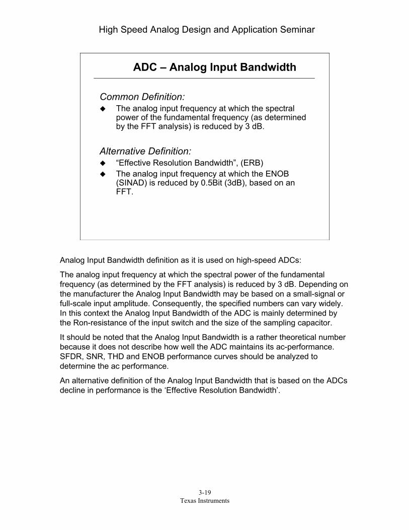
Common Definition:The analog input frequency at which the spectralpower of the fundamental frequency (as determinedby the FFT analysis) is reduced by 3 dB.
Alternative Definition:“Effective Resolution Bandwidth”, (ERB)The analog input frequency at which the ENOB(SINAD) is reduced by 0.5Bit (3dB), based on anFFT.
Analog Input Bandwidth definition as it is used on high-speed ADCs:
The analog input frequency at which the spectral power of the fundamentalfrequency (as determined by the FFT analysis) is reduced by 3 dB. Depending onthe manufacturer the Analog Input Bandwidth may be based on a small-signal orfull-scale input amplitude. Consequently, the specified numbers can vary widely.In this context the Analog Input Bandwidth of the ADC is mainly determined bythe Ron-resistance of the input switch and the size of the sampling capacitor.
It should be noted that the Analog Input Bandwidth is a rather theoretical numberbecause it does not describe how well the ADC maintains its ac-performance.SFDR, SNR, THD and ENOB performance curves should be analyzed todetermine the ac performance.
An alternative definition of the Analog Input Bandwidth that is based on the ADCsdecline in performance is the ‘Effective Resolution Bandwidth’.

High Speed Analog Design and Application Seminar
3-20Texas Instruments
ADC – Analog Input Bandwidth
Large Signal vs Small SignalInput S&H of ADC determines the inputbandwidthFull-Power Bandwidth is directly related tothe Full-Scale Input Range of the ADC
FPBW is a ‘theoretical’ number
Analog Input Bandwidth
The S&H performance of an ADC is the most significant function thatdetermines the input bandwidth:
The slew-rate capability of the S&H determines the ‘Full-powerBandwidth’ (FPBW) for large signals, typically with the inputamplitude set near full-scale (-1dBFS).
The frequency response of the S&H determines the small signalbandwidth for small signals. The input signal amplitude issignificantly below FS, for example at -20dBFS.
Typically, when specifying the ‘Analog Input Bandwidth’ of an ADC, it isbased on the Full-Power Bandwidth. It is directly related to the full-scaleinput range of the ADC and therefore can be used as an initial selectioncriteria when comparing converter for their undersampling capabilities.

High Speed Analog Design and Application Seminar
3-21Texas Instruments
ADC – Analog Input Bandwidth
G -
Gai
n - d
BFS
0
-2
-4
-6
-8
-101 10 100 1000
f - Input Frequency - MHz
ADS5421
FPBW approx. 550MHzADS5421 14-bit , 40MSPS Pipeline ADC
fsfs/2
Shown here is the frequency response of the ADS5421, a 14-Bit, 40Mspspipeline A/D converter as an example of its ‘Analog Input Bandwidth’. ThisCMOS converter uses a differential sample-and-hold circuit. The switchedcapacitor architecture allows for a very wide analog input bandwidth.
Also indicated by the red line markers are the Nyquist frequency at 20MHz,and the sampling frequency at 40MHz.
The information obtained out of such a bandwidth is that one can estimatethe attenuation to the input signal based on the ADCs frequency response.For example, inputting a 200MHz signal into the ADS5421 would cause anattenuation of about 0.5dB.
Again, there is no indication on what the dynamic performance will be atthis high input frequency. Specifying an ‘Effective Resolution Bandwidth’would make this connection.

High Speed Analog Design and Application Seminar
3-22Texas Instruments
4V
Over-range condition
Sample taken
2.5V
6 Clock cyclelatency
n n+1 n+2
n n+1 n+2
Sample isover-range,invalid data
Valid dataValid data
outputdata
clock
Input
1V
ADC – Input Overload Recovery
OVERVOLTAGE RECOVERY TIME
There is no one condition, except that the signal amplitude must stay below thesupply voltage. If the ADC has internal ESD diodes on its inputs they may start toconduct. For most CMOS based design this is usually 0.3V above and below thesupply rails. If the input voltage exceeds the full-scale range of the ADC the inputcapacitors of the input S&H are still being charged to reflect that value. Assumingnow, the overload condition instantly disappears, within one clock cycle thecharge on the input caps will be removed and biased back to a normal value. Itwill take as many pipeline delays as the converter has until valid data is availableon the data outputs. In this example it will take 6 clock cycles.

High Speed Analog Design and Application Seminar
3-23Texas Instruments
ADC – Input Overload Recovery
Vinput < VsupplyPeak input voltage exceeds specified full-scale ADC input range,
but remains within the supply rails:ADC output at all ‘1’ or ‘0’ during overloadOnce overload condition removed, ADC acquires new validsample with the next clock cycle
Vinput > VsupplyPeak input voltage exceeds the supply rail(s):
ADC output at all ‘1’ or ‘0’ during overloadInternal ESD diodes may conduct and short circuit signal
DC-coupled input configuration:Possible excessive current flowPossibility of damage – need to add external protection, e.g. R’sand diodes, or Voltage Limiting Amplifier (e.g.OPA698)
Two cases:
When the input voltage at any pin exceeds the power supplies (that is,VIN < AGND or VIN > VA or VD), the current at that pin should be limited to lessthan 10mA.

High Speed Analog Design and Application Seminar
3-24Texas Instruments
ADC References
High Speed Analog Design and Application Seminar
3-25Texas Instruments
High-Speed ADC References
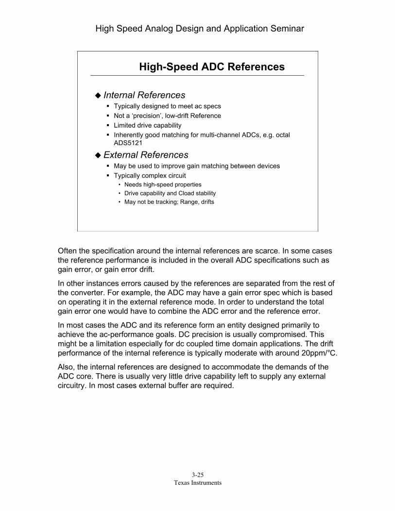
Internal ReferencesTypically designed to meet ac specsNot a ‘precision’, low-drift ReferenceLimited drive capabilityInherently good matching for multi-channel ADCs, e.g. octalADS5121
External ReferencesMay be used to improve gain matching between devicesTypically complex circuit
• Needs high-speed properties• Drive capability and Cload stability• May not be tracking; Range, drifts
Often the specification around the internal references are scarce. In some casesthe reference performance is included in the overall ADC specifications such asgain error, or gain error drift.
In other instances errors caused by the references are separated from the rest ofthe converter. For example, the ADC may have a gain error spec which is basedon operating it in the external reference mode. In order to understand the totalgain error one would have to combine the ADC error and the reference error.
In most cases the ADC and its reference form an entity designed primarily toachieve the ac-performance goals. DC precision is usually compromised. Thismight be a limitation especially for dc coupled time domain applications. The driftperformance of the internal reference is typically moderate with around 20ppm/°C.
Also, the internal references are designed to accommodate the demands of theADC core. There is usually very little drive capability left to supply any externalcircuitry. In most cases external buffer are required.
High Speed Analog Design and Application Seminar
3-26Texas Instruments
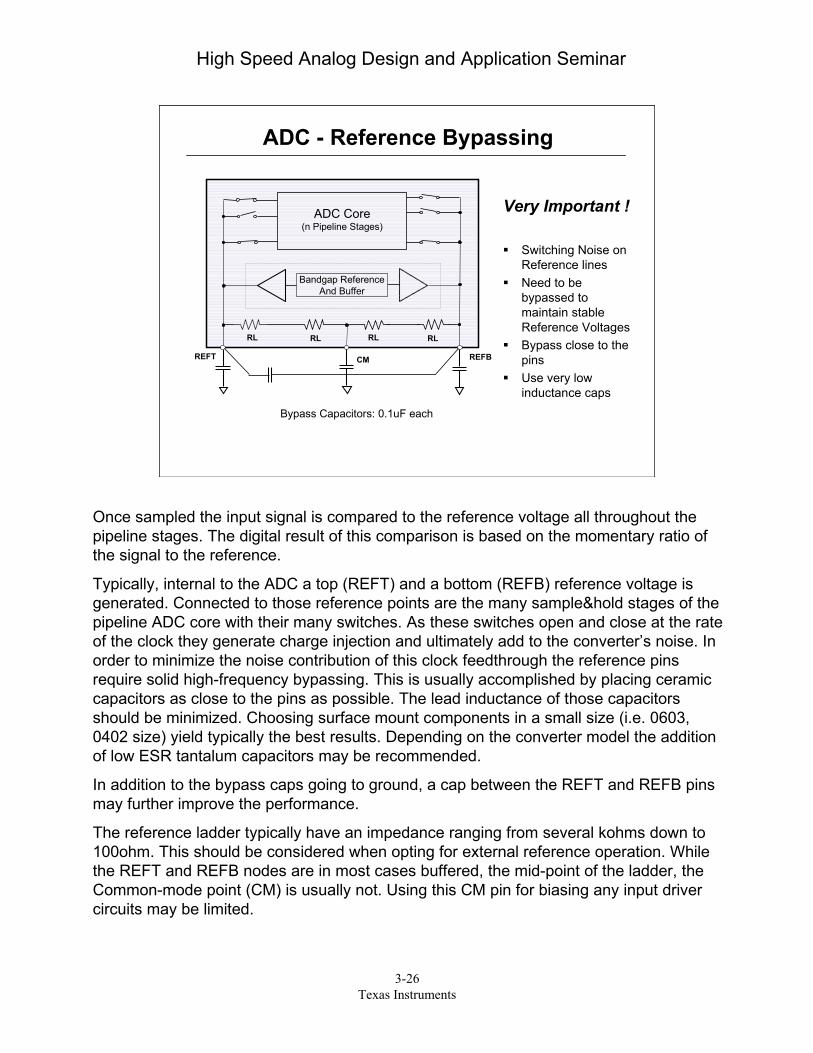
ADC - Reference Bypassing
Very Important !
Switching Noise onReference linesNeed to bebypassed tomaintain stableReference VoltagesBypass close to thepinsUse very lowinductance caps
REFT CM REFB
Bandgap ReferenceAnd Buffer
RL
Bypass Capacitors: 0.1uF each
RL RL RL
ADC Core(n Pipeline Stages)
Once sampled the input signal is compared to the reference voltage all throughout thepipeline stages. The digital result of this comparison is based on the momentary ratio ofthe signal to the reference.
Typically, internal to the ADC a top (REFT) and a bottom (REFB) reference voltage isgenerated. Connected to those reference points are the many sample&hold stages of thepipeline ADC core with their many switches. As these switches open and close at the rateof the clock they generate charge injection and ultimately add to the converter’s noise. Inorder to minimize the noise contribution of this clock feedthrough the reference pinsrequire solid high-frequency bypassing. This is usually accomplished by placing ceramiccapacitors as close to the pins as possible. The lead inductance of those capacitorsshould be minimized. Choosing surface mount components in a small size (i.e. 0603,0402 size) yield typically the best results. Depending on the converter model the additionof low ESR tantalum capacitors may be recommended.
In addition to the bypass caps going to ground, a cap between the REFT and REFB pinsmay further improve the performance.
The reference ladder typically have an impedance ranging from several kohms down to100ohm. This should be considered when opting for external reference operation. Whilethe REFT and REFB nodes are in most cases buffered, the mid-point of the ladder, theCommon-mode point (CM) is usually not. Using this CM pin for biasing any input drivercircuits may be limited.
High Speed Analog Design and Application Seminar
3-27Texas Instruments
Clock Considerations

High Speed Analog Design and Application Seminar
3-28Texas Instruments
ADC Clock ConsiderationsClock Quality a Major Factor for achieving high Dynamic
Performance!
Very low Jitter required to maintain good SNR
• Especially at high Input Frequencies (IF)
SNRj = 20log 2π x fIN x taj taj = rms aperture jitterfIN = Input Frequency
1
• Independent Jitter Sources sum by Root-Sum square
tajtot = √ (tajADC2 + tajExt
2 ) [psrms]
The degradation in SNR is dependent on the input frequency and the totalaperture jitter.
Since jitter is a random occurrence and sources are typically not correlatedthey add by calculating the square-root of the sum of the squares.
The slew-rate (dv/dt) of undersampled IF input signals is very high.Consequently, the effect of clock jitter is pronounced and thereforerequires special consideration.

High Speed Analog Design and Application Seminar
3-29Texas Instruments
ADC Clock ConsiderationsClock ‘Quality’
Use Differential Clock SignalObserve symmetry of Clock line and ImpedancesFast rise/fall timesUse 50% Duty Cycle at max. Sampling Rate
• less important, if A/D operated below max. sampling rateMaintain Clock within the recommended range
• Amplitude (Vp-p), and Common-Mode Level (VCM)• Use proper Termination Techniques to avoid Reflections• Avoid any Over- or Undershoot
Use higher turns ratio for Transformer coupled Circuit to increaseamplitude
Consider using logic circuits that have sufficiently fast rise and fall times(1ns) to minimize their contribution to the total jitter error.
If this option is available, the ADC’s clock input should be drivendifferentially. Applying a single-ended clock to differential clock inputs maynot yield the optimum performance due to asymmetric rsie and fall timesthat will also affect the duty cycle.
If the A/D converter is operated below its maximum sampling rate the dutycycle requirement for the converter clock may be relaxed, meaning it canvary from the ideal 50% point.
High Speed Analog Design and Application Seminar
3-30Texas Instruments
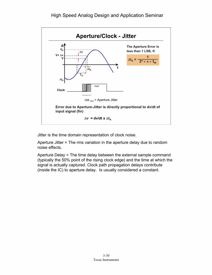
The Aperture Error isless than 1 LSB, if:
ΔtA < 12n × π × fIN
t
A
V
VP
-VP
TA
ΔtA
ΔvV+ Δv
Error due to Aperture-Jitter is directly proportional to dv/dt ofinput signal (fin)
Aperture/Clock - Jitter
Δv = dv/dt x ΔtA
ClockHold
Δta rms = Aperture Jitter
Jitter is the time domain representation of clock noise.
Aperture Jitter = The rms variation in the aperture delay due to randomnoise effects.
Aperture Delay = The time delay between the external sample command(typically the 50% point of the rising clock edge) and the time at which thesignal is actually captured. Clock path propagation delays contribute(inside the IC) to aperture delay. Is usually considered a constant.
High Speed Analog Design and Application Seminar
3-31Texas Instruments
Clock Jitter Effects
Good clock source Not so good clock source
Comparison of Different Clock Sources
4.5 MHz
Undersampling a 71MHz input signal shows the jitter impact
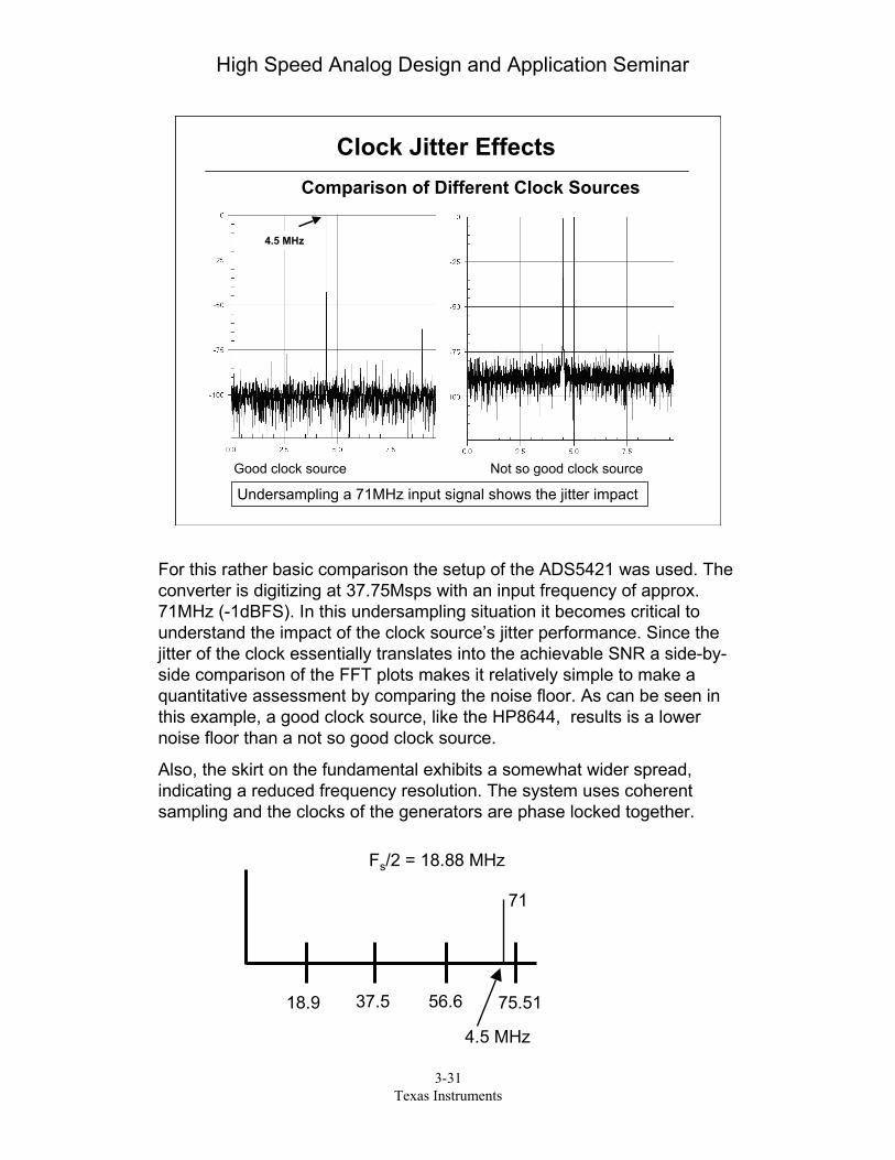
For this rather basic comparison the setup of the ADS5421 was used. Theconverter is digitizing at 37.75Msps with an input frequency of approx.71MHz (-1dBFS). In this undersampling situation it becomes critical tounderstand the impact of the clock source’s jitter performance. Since thejitter of the clock essentially translates into the achievable SNR a side-by-side comparison of the FFT plots makes it relatively simple to make aquantitative assessment by comparing the noise floor. As can be seen inthis example, a good clock source, like the HP8644, results is a lowernoise floor than a not so good clock source.
Also, the skirt on the fundamental exhibits a somewhat wider spread,indicating a reduced frequency resolution. The system uses coherentsampling and the clocks of the generators are phase locked together.
Fs/2 = 18.88 MHz
18.9 37.5 56.6 75.51
71
4.5 MHz

High Speed Analog Design and Application Seminar
3-32Texas Instruments
Notes on Clock & Jitter 1
If the noise floor (SNR) appears to be higher thanexpected when evaluating a High-Speed ADC(FFT plot), check the jitter contribution of the clocksource
Typically, higher frequency crystal clocks(fc>10MHz) have a low jitter of less than 10ps rms
Lower frequency clocks usually have higher jitter
Therefore, consider a higher Fc and divide down
Dividing a higher frequency clock can be beneficial, however eachadditional logic gate etc. can potentially add phase noise and mayincrease the total jitter. Therefore, division factors are usually limited to 8or less. This also depends on the clock source and desired end frequency.

High Speed Analog Design and Application Seminar
3-33Texas Instruments
Notes on Clock & Jitter 2
Clocks from FPGAs, uP, DSP etc., are usually notsuitable for high-speed converter, especially not forundersampling applications
Noise on the ADC power supply directly affects theinternal clock circuitry and may lead to increased jitter
Noise and spurs on the clock will be ‘mixed’ duringsampling and lead to a decrease in dynamic range
Many A/D converters now feature differential clockinput designed for sine-, and square wave inputs
Don’t route clock line parallel to other signal lines
Clock signal may be band limited (BP filtered) to reduce existing spursand noise before applying to the ADC.
High Speed Analog Design and Application Seminar
3-34Texas Instruments
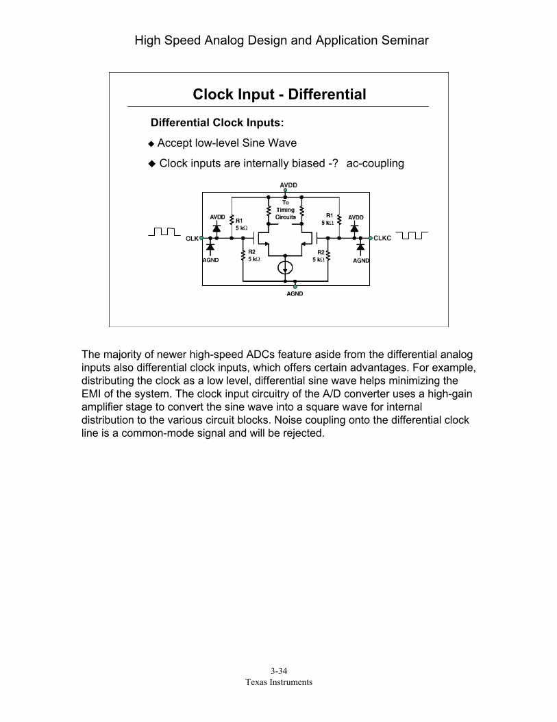
Clock Input - Differential
Differential Clock Inputs:
Accept low-level Sine Wave
Clock inputs are internally biased -? ac-coupling
The majority of newer high-speed ADCs feature aside from the differential analoginputs also differential clock inputs, which offers certain advantages. For example,distributing the clock as a low level, differential sine wave helps minimizing theEMI of the system. The clock input circuitry of the A/D converter uses a high-gainamplifier stage to convert the sine wave into a square wave for internaldistribution to the various circuit blocks. Noise coupling onto the differential clockline is a common-mode signal and will be rejected.
High Speed Analog Design and Application Seminar
3-35Texas Instruments
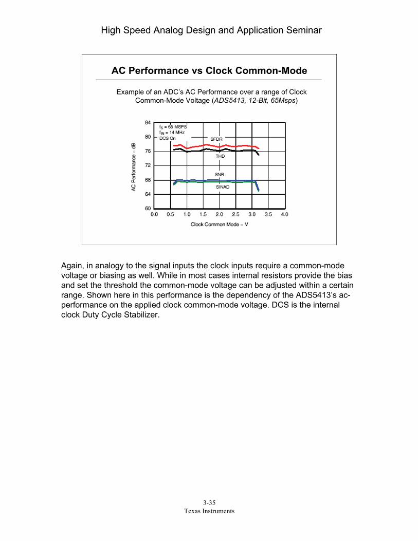
AC Performance vs Clock Common-Mode
Example of an ADC’s AC Performance over a range of ClockCommon-Mode Voltage (ADS5413, 12-Bit, 65Msps)
Again, in analogy to the signal inputs the clock inputs require a common-modevoltage or biasing as well. While in most cases internal resistors provide the biasand set the threshold the common-mode voltage can be adjusted within a certainrange. Shown here in this performance is the dependency of the ADS5413’s ac-performance on the applied clock common-mode voltage. DCS is the internalclock Duty Cycle Stabilizer.
High Speed Analog Design and Application Seminar
3-36Texas Instruments
CLK
CLKADC
0.01nFTTL/CMOS Clock Source(3V/5V)
Clock Driver - Examples
CLK
CLK
ADCSquare waveClock Source
0.01uF
1:1Rs
RT
1. Single-Ended
2. Differential
0.01nF
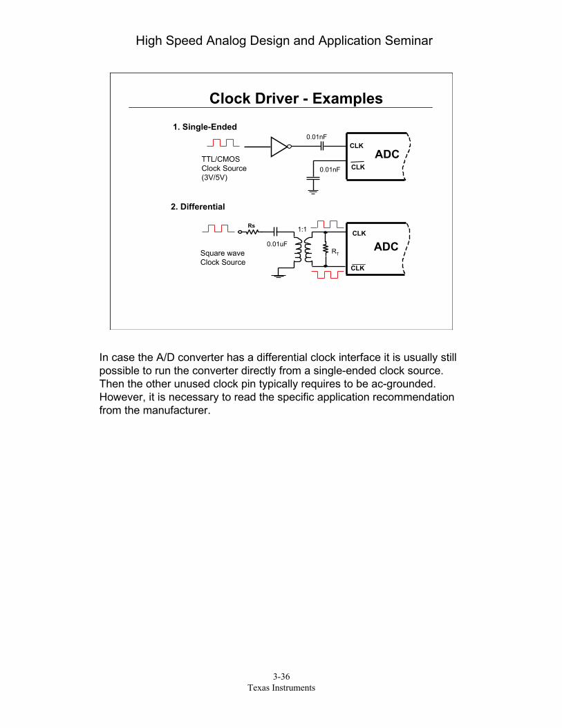
In case the A/D converter has a differential clock interface it is usually stillpossible to run the converter directly from a single-ended clock source.Then the other unused clock pin typically requires to be ac-grounded.However, it is necessary to read the specific application recommendationfrom the manufacturer.

High Speed Analog Design and Application Seminar
3-37Texas Instruments
Clock Driver - Examples
0.01μF
100Ω
Clock Driver: CDCM1804, CDCP1803,CDC7005; or other PECL translatordevices
+ 5V
ADC
Sine WaveInput
CLK2
3
78
54
CLK6
0.01μF100Ω
0.01μF50Ω
Sine Wave to TTL Conversion, Differential

High Speed Analog Design and Application Seminar
3-38Texas Instruments
Minimum Sampling Frequency
Sampling Capacitor Values typically < 1pF Non-ideal Components Internal Leakage Current
Causes Droop
Requires a Minimum Sampling Frequency to Move Signal Charge and ‘Refresh’ the Capacitors to a Defined Voltage (VCM).
High-Speed Pipeline ADC
Datasheets of High-Speed Pipeline ADCs often specify a ‘Minimum SamplingFrequency’, and this frequently prompt the questions why that is and whathappens if the clock frequency drops below the specified value. Back when theSample&Hold stage had to be implemented with an external Sample&Holdamplifier one big concern was the droop rate, which is a functions of the Holdtime and the capacitor size. The on-chip Sample&Hold circuit has just the sameconstraints. The size of the sampling capacitor is very small and internal leakagecurrents (charge) can affect the charge representing the actual sample. As thesampling frequency is reduced the hold time becomes longer and droop occurs.

High Speed Analog Design and Application Seminar
3-39Texas Instruments
Non-Continuous Clocking
Burst-Mode Operation possible on some ADCs
Observe Minimum Clock Requirement for Uninterrupted,Continuous Sampling. Typically: fsmin >1MHz.Data in Pipeline may become Invalid if Clock is Stopped for aLonger than specified Time.Some ADCs may go into an automatic power-down mode ifsampling rate drops below a certain limitWill not work with ADCs that have internal clock stabilizer,which is usually DLL based.
Operating the ADC within certain clock conditions is typically required in order toobtain the specified dynamic performance. One of those clock conditions is todeliver a 50% clock duty cycle to the converter, a requirement particularlyimportant towards the maximum sampling rate. To ease this requirement for thesystems designer, newer ADC model incorporate a clock duty cycle stabilizercircuit. Those circuits typically look at the sampling clock edge, e.g. the risingedge, as a reference and retime the non-sampling edge, providing an internalclock that maintains a fixed 50% duty cycle. The advantage is that it allows awide range of clock input duty cycles without compromising the ADC’sperformance. Such duty cycle stabilizer typically use delay-locked loops (DLL). Asa result, any change in the applied sampling rate requires the DLL to acquire andlock to the new rate, which can take up to several hundred clock cycles. For thatreason such an ADC may not be the right choice for applications that require afast response to instantaneous changes in the sampling rate.

High Speed Analog Design and Application Seminar
3-40Texas Instruments
Minimum Clock Requirement
a.
tH tL
tCONV
b.
tHtL
Minimum Clock Width Requirement tH, tL 2tCONVmax
tH tL
tCONVmax
c.
While we discussed before the requirements for a certain duty cycle andmaximum, or minimum sampling frequency it comes down to a ‘Minimum ClockPulse Width’ requirement.
Shown in a) is the clock signal as it is required to run the ADC at its maximumsampling rate – with a duty cycle at or close to 50%.
When operating the ADC below the maximum sampling rate, the duty cycle maydeviate from this requirement to the extent that the minimum clock pulse width issatisfied. Line b. shows the clock high time being the shortest, but no less thanhalf the sampling rate. Line c. has the clock low time being short.
For example: for an ADC with a maximum sampling rate of 40Msps (Clock period= 25ns), the minimum ½ cycle width is 11.25ns.

High Speed Analog Design and Application Seminar
3-41Texas Instruments
ADS5413 Duty-Cycle Sensitivity
Shown here is the duty-cycle sensitivity of the ADS5413, a 12-Bit 65MspsPipeline A/D converter. This particular model employs an internal clock duty-cyclestabilizer (DCA). While it’s performance holds up fairly well with this stabilizerbeing inactive, it further improves the performance towards the extreme ends ofthe duty-cycle.

High Speed Analog Design and Application Seminar
3-42Texas Instruments
Power Consumption vs. Fclk
Supply Current (I) versus CLK
0
50
100
150
200
250
300
350
1 5 10 15 20 25 30 35 40
S A MP LE R A TE ( MS P S )
IAVDD (mA) IDVDD (mA) IDRVDD (mA)
In general, the power consumption on (High-Speed) converters do not scalelinearly, even though their CMOS nature may imply this. While 'scaling' is true forpure logic devices, converter are essentially 'analog' components. The internalcircuits devices need biasing in order to achieve the maximum speed theconverter is designed for. Therefore most of the supply current is a constantcurrent and is not affected by the clock speed. On almost all of the high-speedconverter, only about 20% to 30% of the total power consumption is affected by achange in the clock speed.
The shown curves are taken on the ADS5120, an eight-channel, 10-Bit, 40MspsPipeline converter operating on a low 1.8V supply (3.3V output driver supply).
High Speed Analog Design and Application Seminar
3-43Texas Instruments
ADC’s Digital Data Output

High Speed Analog Design and Application Seminar
3-44Texas Instruments
Digital Data Outputs of HS- ADCs
Usually has only Limited Output DriveTyp. around 15mA per Output
External Latches or Buffers Recommended
Dedicated Output Driver Supply Pin (VDRV)Allows Flexible Interfacing to +5V/+3.3V/+1.8V LogicIVDRV = VDRV x fclk x CL x N (worst case)
• CL = load capacitance• N = number of data output pins
The maximum output driver current flows when all outputs are switching on everyclock cycle, e.g. when a full-scale square wave signal is applied. While this is arather theoretical case, the sampling rate along with the characteristics of theinput signal will result in an average number of bits switching.

High Speed Analog Design and Application Seminar
3-45Texas Instruments
Shown here is the simplified model of an digital output driver within theADC’s output stage. Here the upper transistor will charge the load(capacitive, CL) while drawing the current from the supply pin +VDRV. Thelower transistor will be active for discharging the load capacitance. Thischarge will be conducted to the converter’s ground (possibly the substrate),and due to it’s finite resistance it may momentarily raise the groundpotential. This could effectively add noise degrading the noiseperformance of the converter. When transitioning from logic ‘L’ to ‘H’ or ‘H’to ‘L’, a high transient current flows through the output MOSFETs eitherfrom the +VDRV supply or to ground. This current depends on thecapacitive loading (CL), according to Iout = C dv/dt.
Therefore, a large capacitive load (parasitic) can create a large current toflow in the output stage and cause a current spike in the supplies.
CL
+VDRV
Iout proportional to CL !
Iout = C dvdt
dvdt
Digital Data Outputs of HS- ADCs
Z ⇒Δ VImpedance of ‘chip’ ground causes voltagedrop and therefore ‘ground bounce’

High Speed Analog Design and Application Seminar
3-46Texas Instruments
Capacitive Loading of Digital Outputs
Limit capacitive loading to <15pF for each output pin
Datasheet Specifications use 10pF total output loading:5pF - pcb parasitics5pF - input capacitance of one logic gate
Typical output slew rate of logic gate is 0.8V/ns.
Example: 15pF x 0.8V/ns = 12mA
Digital Data Outputs of HS- ADCs
The current requirements for the output driver of the ADC is directly proportionalto its capacitive loading. Hence the requirement for keeping the capacitive loadingas low as possible. However, with a target of keeping the loading at one pin toless than 10 or 15pF, it is easy to accumulate this quickly.

High Speed Analog Design and Application Seminar
3-47Texas Instruments
Capacitive Loading of Digital Outputs
Example: Data Output with CL = 15pF, VDRV = +5V/+3V
+5V
+3V
0V
Increased Output Loading results in ‘Sawtooth’ shaped Output
Excess capacitive loading will alter the time constant and could eventuallyprevent from the data capture window being sufficient. Or, the required thresholdlevels are no longer being crossed. It is often recommended to insert small seriesresistor between the ADC’s data outputs and the following logic device. While thismethod can help avoiding possible over- and undershoot and limit theinstantaneous current, a too high of a value can be detrimental.

High Speed Analog Design and Application Seminar
3-48Texas Instruments
What’s New? …….LVDS!
Low Voltage Differential SignalingHigh-Speed, Low Power Data TransmissionStandardDifferential Output Swing is 350mVp-p (typ.)Current mode (Iout =3.5mA)100Ω Differential Termination at ReceiverVCM =1.2V, VH = 1.38V, VL = 1.03V
ANSI/TIA/EIA-644 Standard
Only defines driver output and receiver input characteristics
Provides guidelines for bus configuration, cables and termination
Does not define protocol, connectors, and bus structure
Does not define a maximum data rate
Newer standard (ANSI/TIA/EIA-644-A): multiple receivers
High Speed Analog Design and Application Seminar
3-49Texas Instruments
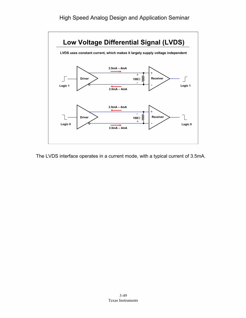
Low Voltage Differential Signal (LVDS)
3.5mA – 4mA
3.5mA – 4mA
+
-100Ω
Logic 1 Logic 1
3.5mA – 4mA
3.5mA – 4mA
-
+100Ω
Logic 0 Logic 0
Driver
Driver
Receiver
Receiver
+
-
+
-
LVDS uses constant current, which makes it largely supply voltage independent
The LVDS interface operates in a current mode, with a typical current of 3.5mA.
High Speed Analog Design and Application Seminar
3-50Texas Instruments
LVDS Advantages
Allows low noise/ low EMI system design
It is supply independent Easy migration path to lower supply voltages
Class A operation has low dI/dt noise
Wide common mode range Better common-mode noise immunity.
Advantages compared to LVTTL, LVCMOS, or (P)ECL
Fewer pins for higher resolution
Reduced Signal Swing
Lower Noise Interface for Data Converter
Lower EMI
Higher Data Rates Possible
Lower Voltage Supplies

High Speed Analog Design and Application Seminar
3-51Texas Instruments
LVDS: Parallel vs. Serial
ReceiverTransmitter
Par
alle
l Dat
a
Par
alle
l Dat
a
Clock Clock
ReceiverTransmitter
Parallel Data Serializer Parallel DataDeserializer
Clock Clock
Transmitter Receiver
Parallel Data Serializer Parallel DataDeserializer
Clock ClockPLL
a) Non-Embedded Clock
b) Embedded Clock
Parallel LVDS Serialized LVDS
There a three possible implementations of an LVDS interface. The first is usingLVDS for each data pin resulting in ‘Parallel LVDS’. Compared to a single-endedCMOS interface this will double the number of interface lines between thetransmitter and receiver. If a large number of channels is required this couldbecome a severe restriction. Here, implementing a serial LVDS interface wouldreduce the number of required lines significantly. Serialized LVDS interfaces cancome in two types: one is the ‘non-embedded clock’, the other uses an embeddedclock.

High Speed Analog Design and Application Seminar
3-52Texas Instruments
Serialized LVDS - Formats
Non-Embedded ClockNo special data formatNo PLL needed in receiver to recover dataCan implement Double Data Rate (DDR)More I/O lines needed
Embedded ClockSpecial data format (8b/10b)Higher transmission speed required for same amount of dataPLL required in receiver, which increases complexityFewer I/O lines needed
High Speed Analog Design and Application Seminar
3-53Texas Instruments
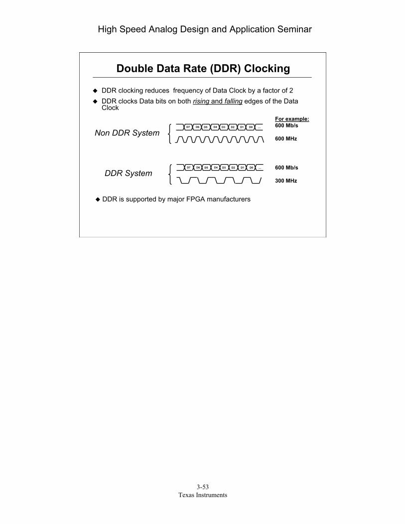
Double Data Rate (DDR) Clocking
DDR clocking reduces frequency of Data Clock by a factor of 2DDR clocks Data bits on both rising and falling edges of the DataClock
Non DDR System
DDR System
D4 D3 D2 D1 D0 …D5D6D7
D4 D3 D2 D1 D0 …D5D6D7
For example:600 Mb/s
600 MHz
600 Mb/s
300 MHz
DDR is supported by major FPGA manufacturers
High Speed Analog Design and Application Seminar
3-54Texas Instruments
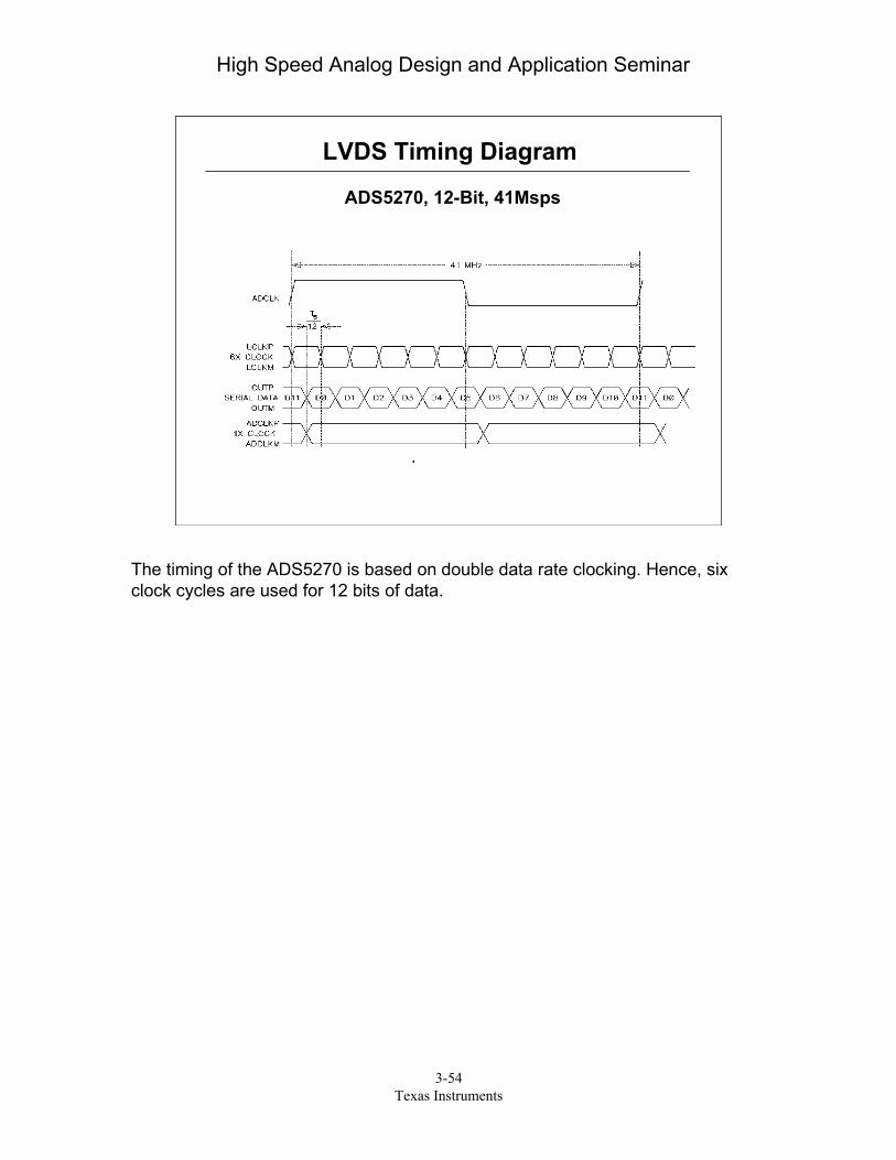
LVDS Timing Diagram
ADS5270, 12-Bit, 41Msps
The timing of the ADS5270 is based on double data rate clocking. Hence, sixclock cycles are used for 12 bits of data.

High Speed Analog Design and Application Seminar
3-55Texas Instruments
ADS5270, ADS5271
Features
Key SpecsADS5270 Parameters Min Typ Max Unit
Analog Supply 3 3.3 3.6 VDigital Supply 3 3.3 3.6 V
SNR @ Fin = 10MHz 68 70 dBSFDR @ Fin = 10MHz 85 dB
Total Power 950 mW
HTQFP-80
40/50 MSPS Sample Rate8 Simultaneous Sample and HoldLVDS Data Clock and Word Clock OutputsSerialized LVDS OutputsInternal and External ReferencesSamples availableIntroduced
8-Channel 40/50 MSPS 12-Bit ADCs withLVDS Interface
12-bit41 MSPS
ADCS/H
D LL
12-bit41 MSPS
ADCS/H
12-bit41 MSPS
ADCS/H
12-bit41 MSPS
ADCS/H
12-bit41 MSPS
ADCS/H
12-bit41 MSPS
ADCS/H
12-bit41 MSPS
ADCS/H
12-bit41 MSPS
ADCS/H
R ef erence
Serializer
Serializer
6X A DCLK
1X A DCLK
Serializer
Serializer
Serializer
Serializer
Serializer
Serializer
A DCLK
IN P1
IN N1
INT/
EXT
REF
P
VCM
REF
M
OUT P1OUT N1
LCLKPLCLKM
A DCLKPA DCLKM
INP2
IN N 2
INP3
IN N 3
INP4
IN N 4
INP5
IN N 5
INP6
IN N 6
INP7
IN N 7
INP8
IN N 8
OUT P2OUT N2
OUT P3OUT N3
OUT P4OUT N4
OUT P5OUT N5
OUT P6OUT N6
OUT P7OUT N7
OUT P8OUT N8

High Speed Analog Design and Application Seminar
3-56Texas Instruments
LVDS ADC and Deserializer EVMs
ADS527x
Sam
tec
Bot
Input CircuitryMicro
DB9
CM
OS
CM
OS
CMOS
CMOS
CM
OS
CM
OS
CMOS
CMOS
Xilinx FPGA
Sam
tec
Top
JTAG EPROM
CLK
Input Circuitry
RS232-TTL
Yellow LED
Orange LED
Red LED
Green LED
Int/ Ext Refernece Select pushbutton
Int/ Ext Refernece LED (on = Int)
Serial Interface (on = data)
Power down LED
Reset LED
Power down pushbutton
Reset pushbutton
Pow
erC
onne
ctor
s
Resetpushbutton
Programpushbutton
PowerConnectors
Done LED(green)
Gre
enPo
wer
LED
ADS527x family: 10-/12-Bit, 40/50Msps8-Channel ADCs with serialized LVDS
High Speed Analog Design and Application Seminar
3-57Texas Instruments
Appendix
– HS-ADC Testing– Pipeline Architecture, Basic Overview
High Speed Analog Design and Application Seminar
3-58Texas Instruments
Typical ADC Bench Test Setup
ADC
EvaluationModule
Signal GeneratorLow distortion
Sine Wave(HP8644)
Signal GeneratorLow jitter Clock
(HP8644)
FilterBP, LP
FFT,Logic
Analyzer(TLA714)
PC
Data
PowerSupplies
Fclock
FinFin
*Generators are phase-lockedFor coherent sampling
Fclock
IEEE Bus ConnectionControlled by TLA
*
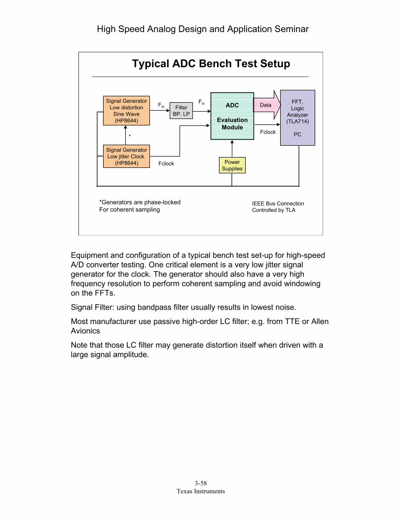
Equipment and configuration of a typical bench test set-up for high-speedA/D converter testing. One critical element is a very low jitter signalgenerator for the clock. The generator should also have a very highfrequency resolution to perform coherent sampling and avoid windowingon the FFTs.
Signal Filter: using bandpass filter usually results in lowest noise.
Most manufacturer use passive high-order LC filter; e.g. from TTE or AllenAvionics
Note that those LC filter may generate distortion itself when driven with alarge signal amplitude.
High Speed Analog Design and Application Seminar
3-59Texas Instruments
ADC Performance Specifications
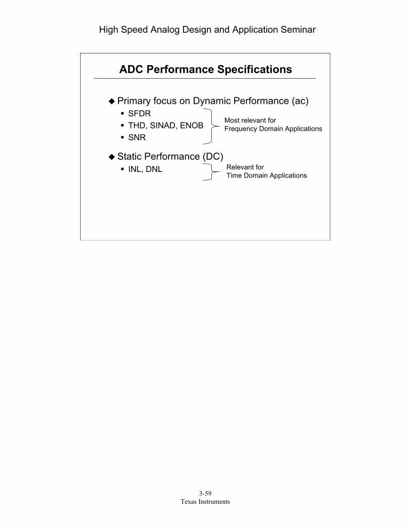
Primary focus on Dynamic Performance (ac)SFDRTHD, SINAD, ENOBSNR
Static Performance (DC)INL, DNL
Most relevant for Frequency Domain Applications
Relevant for Time Domain Applications

High Speed Analog Design and Application Seminar
3-60Texas Instruments
What’s the Application/EE ?Time Domain
Imaging (CCD)CamcordersDigital CamerasScannerRGB/Comp. VideoTest InstrumentationMedical
Important Specs:SNRSlew-Rate/ tsetDNLDC-Accuracy/ Drift
Frequency DomainCommunications
Set-Top BoxCable ModemBasestationIF DigitizerGPSFrequency Synthesizer
Important Specs:SFDRENOBAnalog Input BandwithJitter

High Speed Analog Design and Application Seminar
3-61Texas Instruments
ADS5500 – 14-Bit Pipeline A/D

High Speed Analog Design and Application Seminar
3-62Texas Instruments
The last architecture that will be discussed is the pipeline technique, which can beconsidered also another derivative of the “one bit” comparator topology of thesuccessive approximation converter and the “all bits at once” design of the flashADC. As the next logical step after the sub-ranging architecture, pipeline convertersare just beginning to emerge on a broad basis throughout the IC industry, although,the proof of concept was done about eight years ago.
Because of their concurrent digitizing technique pipeline converters achievecomparably high conversion rates. Built as monolithic ICs on CMOS processes oneof their biggest advantage is the low power consumption. Even though pipelineconverters use the flash architecture as a subcircuit in their processing path they donot exhibit the problem with sparkle codes. This is essentially due to the fact thateach flash converter is of low resolution (1 to 2 bits). This means that the number ofcomparators is very small, which results in a good separation of their thresholdvoltages compared to pure flash converter. The appearance of false codes, or“sparkle codes” due to the false trigger of one of the comparators is not an issuewith pipeline A/D converter.
Pipeline A/D Converter
High Conversion Rate, fCONV > 200MHzVery Low Power ConsumptionWide Analog Input Bandwidth (>500MHz)Optimized Error CorrectionUsually with Internal Reference (FSR options)Monolithic , small PackagesSwitched Inputs, CapacitiveData LatencyMinimum Clock Frequency
High Speed Analog Design and Application Seminar
3-63Texas Instruments
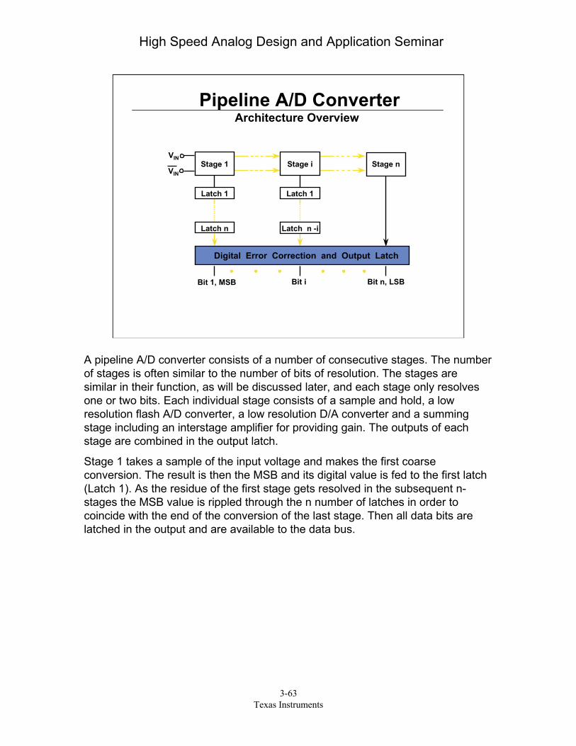
A pipeline A/D converter consists of a number of consecutive stages. The numberof stages is often similar to the number of bits of resolution. The stages aresimilar in their function, as will be discussed later, and each stage only resolvesone or two bits. Each individual stage consists of a sample and hold, a lowresolution flash A/D converter, a low resolution D/A converter and a summingstage including an interstage amplifier for providing gain. The outputs of eachstage are combined in the output latch.
Stage 1 takes a sample of the input voltage and makes the first coarseconversion. The result is then the MSB and its digital value is fed to the first latch(Latch 1). As the residue of the first stage gets resolved in the subsequent n-stages the MSB value is rippled through the n number of latches in order tocoincide with the end of the conversion of the last stage. Then all data bits arelatched in the output and are available to the data bus.
Pipeline A/D ConverterArchitecture Overview
Stage 1 Stage i Stage nVIN
Latch 1
Latch n
Latch 1
Latch n -i
Digital Error Correction and Output Latch
Bit 1, MSB Bit i Bit n, LSB
VIN

High Speed Analog Design and Application Seminar
3-64Texas Instruments
This figure depicts the conceptual blocks inside a pipeline A/D converter. Thestructure is highly repetitive where each of the pipeline stages consists of a S/H,a flash A/D converter, a D/A converter, a subtractor including a gain stage andlatches for delay. Both, the A/D and D/A converter are of low resolution, in thiscase 2 bits. To begin a conversion, the input is sampled and held. The held inputis then converted into a digital code by the first stage low resolution A/D converterand back into an analog signal by the D/A converter. The difference between theD/A output and the held input is the residue that is amplified and sent to the nextstage where this process is repeated. At any instant, while the first stageprocesses the current input sample, the second stage processes the amplifiedresidue of the previous input sample from the first stage. Because sequentialstages simultaneously work on residues from successively sampled inputs, thedigital outputs from each stage correspond to input samples at different times.Digital latches are needed to synchronize the outputs from the n-stages.
Each stage includes an amplifier to amplify the signal before passing it on to thenext stage. The gain error in each of those amplifiers is often the main contributorto the ADCs differential linearity error (DNL).
Pipeline A/D ConverterArchitecture Overview
+ +
- -
VIN
Bit iBit 1, MSB Bit n, LSB
Stage 12-BitA/D
2-BitD/A
Delayn Latches
Σ
Delayn-1 Latches
2-BitA/D
2-BitD/A
ΣS/H2S/H1
Digital Error Correction
Output Latches
Gain = 2
High Speed Analog Design and Application Seminar
3-65Texas Instruments
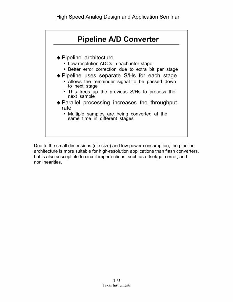
Due to the small dimensions (die size) and low power consumption, the pipelinearchitecture is more suitable for high-resolution applications than flash converters,but is also susceptible to circuit imperfections, such as offset/gain error, andnonlinearities.
Pipeline A/D Converter
Pipeline architectureLow resolution ADCs in each inter-stageBetter error correction due to extra bit per stage
Pipeline uses separate S/Hs for each stageAllows the remainder signal to be passed downto next stageThis frees up the previous S/Hs to process thenext sample
Parallel processing increases the throughputrate
Multiple samples are being converted at thesame time in different stages
High Speed Analog Design and Application Seminar
3-66Texas Instruments
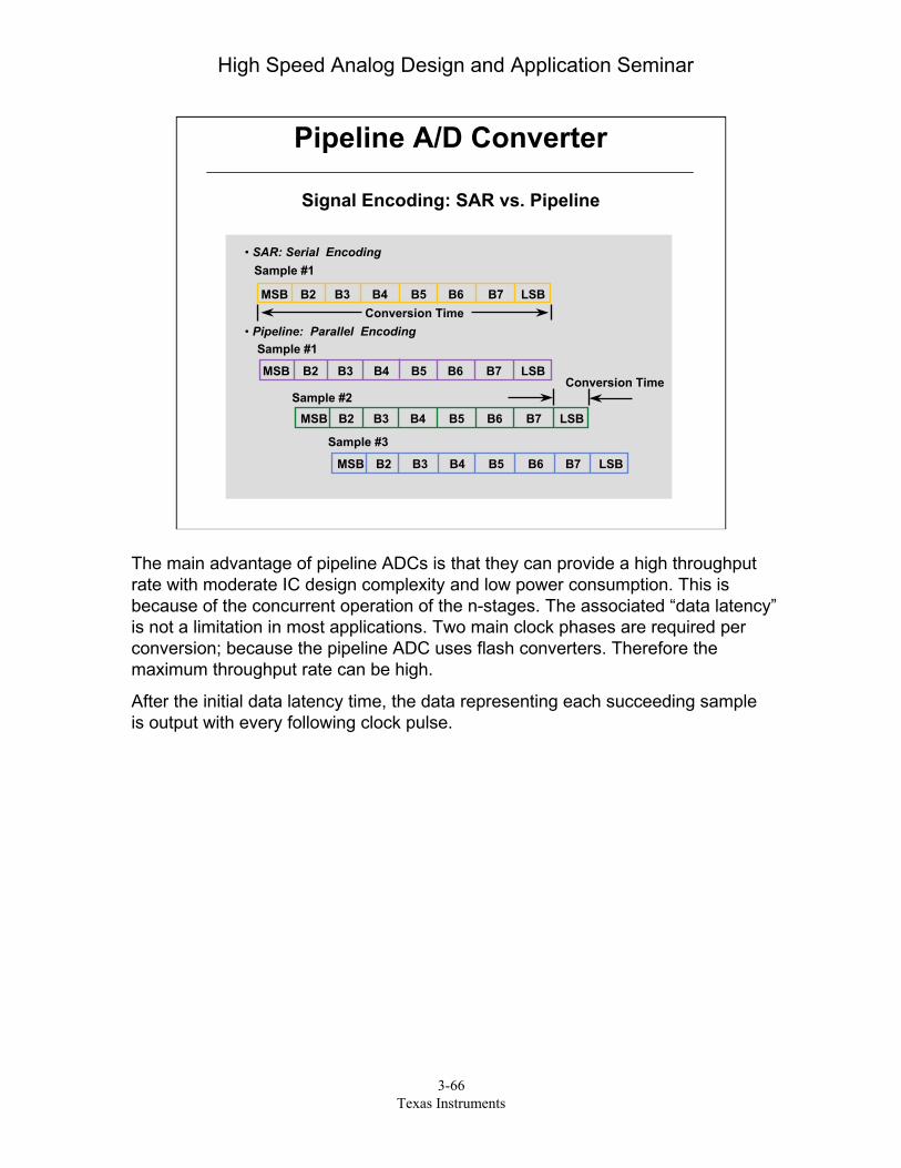
The main advantage of pipeline ADCs is that they can provide a high throughputrate with moderate IC design complexity and low power consumption. This isbecause of the concurrent operation of the n-stages. The associated “data latency”is not a limitation in most applications. Two main clock phases are required perconversion; because the pipeline ADC uses flash converters. Therefore themaximum throughput rate can be high.
After the initial data latency time, the data representing each succeeding sampleis output with every following clock pulse.
MSB LSBB2 B3 B4 B5 B6 B7
LSB
Pipeline A/D Converter
Signal Encoding: SAR vs. Pipeline
• SAR: Serial EncodingSample #1
• Pipeline: Parallel Encoding
Sample #3
Sample #2
Sample #1
MSB
MSB
MSB
LSB
LSB
B2
B2
B2
B3
B3
B3
B4
B4
B4
B5
B5
B5
B6
B6
B6
B7
B7
B7
Conversion Time
Conversion Time

High Speed Analog Design and Application Seminar
3-67Texas Instruments
To obtain the best performance from pipelined A/D converter the designer needsto make careful considerations about the timing and the clock source. This isbasically true for all high speed A/D converter architectures. Clock jitter canintroduce a significant error and needs to be kept low to avoid a degradation ofthe resolution.
With pipeline A/D converter the rising and the falling clock edge are used toinitiate certain operations. Each converter stage in the pipeline will be samplingduring one phase and amplifying in the other phase. The internal S/H clockapplied to each sub-converter is offset by 180° phase from the previous stageclock signal with the result that alternate stages will perform the same operation(concurrent operation).
The duty cycle of the external clock should be held at 50% with a low jitterespecially when digitizing a high frequency input signal and operating themaximum sample rate. A deviation from the 50% duty cycle will effectivelyshorten some of the allowed interstage settling times, thus degrading the SNRand DNL performance.
The first valid digital data of the pipeline architecture will have an associateddelay before it becomes available at the bus. This delay is called “Data Latency”and is dependent on the number of internal converter stages .
Pipeline A/D Converter
Timing and Data Latency
n-7 n-6 n-5 n-4 n-3 n-2 n-1 n
Analog Input
Clock
InternalS/H
Output Data
Sample Points
S1
S2 S3
S4 S5
S6S7
S8S9
Track
Hold
Track
Hold
Data Latency
n+3n n+7n+6n+5n+4n+2n+1

High Speed Analog Design and Application Seminar
3-68Texas Instruments