Embed Size (px)
Citation preview

Section 35. Output Compare with Dedicated Timer
Output Com
pare with
Dedicated Timer
35
HIGHLIGHTSThis section of the manual comprises the following major topics:
35.1 Introduction .................................................................................................................. 35-235.2 Output Compare Registers .......................................................................................... 35-335.3 Modes of Operation ..................................................................................................... 35-735.4 Output Compare Operation in Power-Saving States ................................................. 35-3035.5 I/O Pin Control ........................................................................................................... 35-3035.6 Register Maps............................................................................................................ 35-3135.7 Electrical Specifications ............................................................................................. 35-3235.8 Design Tips ................................................................................................................ 35-3335.9 Related Application Notes.......................................................................................... 35-3435.10 Revision History ......................................................................................................... 35-35
© 2008 Microchip Technology Inc. Advance Information DS39723A-page 35-1
PIC24F Family Reference Manual
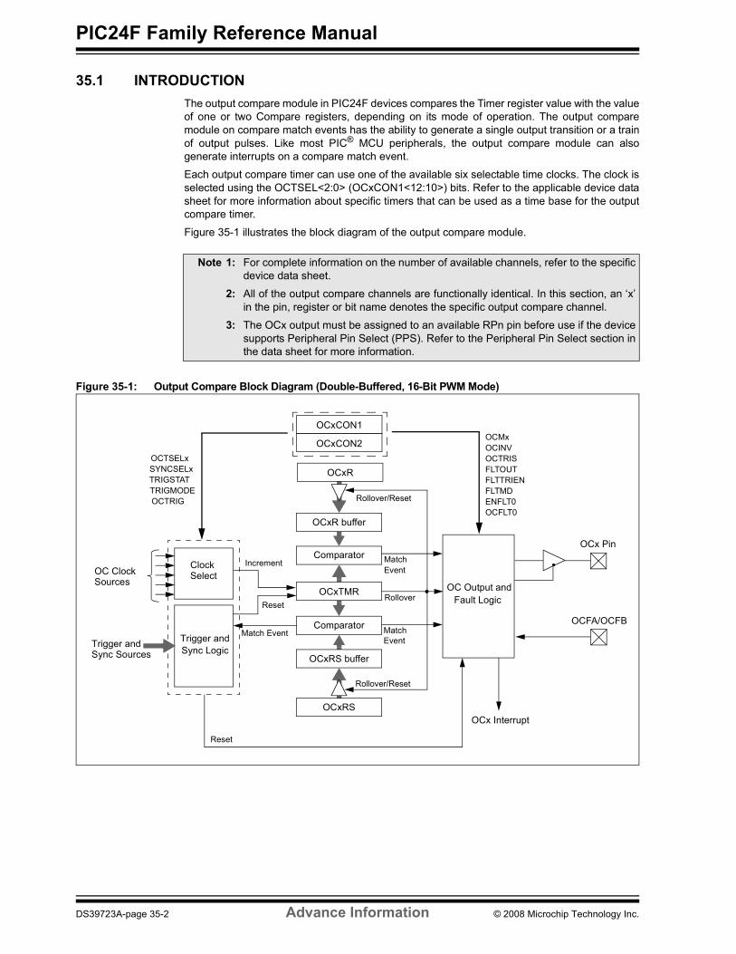
35.1 INTRODUCTIONThe output compare module in PIC24F devices compares the Timer register value with the valueof one or two Compare registers, depending on its mode of operation. The output comparemodule on compare match events has the ability to generate a single output transition or a trainof output pulses. Like most PIC® MCU peripherals, the output compare module can alsogenerate interrupts on a compare match event.
Each output compare timer can use one of the available six selectable time clocks. The clock isselected using the OCTSEL<2:0> (OCxCON1<12:10>) bits. Refer to the applicable device datasheet for more information about specific timers that can be used as a time base for the outputcompare timer.
Figure 35-1 illustrates the block diagram of the output compare module.
Figure 35-1: Output Compare Block Diagram (Double-Buffered, 16-Bit PWM Mode)
Note 1: For complete information on the number of available channels, refer to the specificdevice data sheet.
2: All of the output compare channels are functionally identical. In this section, an �x�in the pin, register or bit name denotes the specific output compare channel.
3: The OCx output must be assigned to an available RPn pin before use if the devicesupports Peripheral Pin Select (PPS). Refer to the Peripheral Pin Select section inthe data sheet for more information.
OCxR buffer
Comparator
OCxTMR
OCxCON1
OCxCON2
OC Output and
OCx Interrupt
OCx Pin
OCxRS buffer
Comparator
Fault Logic
Match
Match Trigger andSync Logic
ClockSelect
Increment
Reset
OC ClockSources
Trigger andSync Sources
Reset
Match EventOCFA/OCFB
OCTSELxSYNCSELxTRIGSTATTRIGMODEOCTRIG
OCMxOCINVOCTRISFLTOUTFLTTRIENFLTMDENFLT0OCFLT0
OCxR
OCxRS
Event
Event
Rollover
Rollover/Reset
Rollover/Reset
DS39723A-page 35-2 Advance Information © 2008 Microchip Technology Inc.

Section 35. Output Compare with Dedicated TimerO
utputCompare
with
Dedicated Timer
35
35.2 OUTPUT COMPARE REGISTERSEach output compare channel is comprised of the following registers:
� OCxCON1 and OCxCON2 � Control registers for the output compare channel� OCxR � Data register for the output compare channel� OCxRS � Secondary Data register for the output compare channel� OCxTMR � The Internal Time Base register
The Control registers for the 9 output compare channels are named OC1CON1 and OC1CON2through OC9CON1 and OC9CON2.
All of the nine control registers have identical bit definitions. They can be represented by acommon register definition as listed in Register 35-1. The �x� in OCxCON1 represents the outputcompare channel number.
Register 35-1: OCxCON1: Output Compare x Control Register 1
U-0 U-0 R/W-0 R/W-0 R/W-0 R/W-0 U-0 U-0� � OCSIDL OCTSEL2 OCTSEL1 OCTSEL0 � �
bit 15 bit 8
R/W-0 U-0 U-0 R/W-0 HCS R/W-0 R/W-0 R/W-0 R/W-0ENFLT0 � � OCFLT0 TRIGMODE OCM2(1) OCM1(1) OCM0(1)
bit 7 bit 0
Legend: HCS = Hardware Clearable/Settable bitR = Readable bit W = Writable bit U = Unimplemented bit, read as �0�-n = Value at POR �1� = Bit is set �0� = Bit is cleared x = Bit is unknown
bit 15-14 Unimplemented: Read as �0�bit 13 OCSIDL: Stop Output Compare x in Idle Mode Control bit
1 = Output compare x halts in CPU Idle mode0 = Output compare x continues to operate in CPU Idle mode
bit 12-10 OCTSEL<2:0>: Output Compare x Clock Select bits111 = Peripheral clock (FCY)110 = Reserved101 = Reserved100 = Timer1 clock (only synchronous clock is supported)011 = Timer5 clock010 = Timer4 clock001 = Timer3 clock000 = Timer2 clock
bit 9-8 Unimplemented: Read as �0�bit 7 ENFLT0: Fault 0 Input Enable bit
1 = Fault inputs are enabled0 = Fault inputs are disabled
bit 6-5 Unimplemented: Read as �0�bit 4 OCFLT0: PWM Fault Condition Status bit
1 = PWM Fault condition has occurred 0 = No PWM Fault condition has occurred
bit 3 TRIGMODE: Trigger Status Mode Select bit1 = TRIGSTAT (OCxCON2<6>) is cleared when OCxRS = OCxTMR or in software0 = TRIGSTAT is cleared only by software
Note 1: The OCx output must also be configured to an available RPn pin if the device supports Peripheral Pin Select. For more information, refer to the specific device data sheet.
2: OCFA pin controls the OC1-OC4 channels; OCFB pin controls the OC5-OC9 channels. OCxR and OCxRS are double-buffered only in PWM modes.
© 2008 Microchip Technology Inc. Advance Information DS39723A-page 35-3

PIC24F Family Reference Manual
bit 2-0 OCM<2:0>: Output Compare Mode Select bits(1)
111 = Center-Aligned PWM mode: Output set high when OCxTMR = OCxR and set low when OCxTMR = OCxRS(2)
110 = Edge-Aligned PWM mode: Output set high when OCxTMR = 0 and set low when OCxTMR = OCxR(2)
101 = Double Compare Continuous Pulse mode: Initialize OCx pin low, toggle OCx state continuouslyon alternate matches of OCxR and OCxRS
100 = Double Compare Single-Shot mode: Initialize OCx pin low, toggle OCx state on matches ofOCxR and OCxRS for one cycle
011 = Single Compare mode: Compare events with OCxR, continuously toggle OCx pin010 = Single Compare Single-Shot mode: Initialize OCx pin high, compare event with OCxR, forces
OCx pin low001 = Single Compare Single-Shot mode: Initialize OCx pin low, compare event with OCxR, forces
OCx pin high000 = Output compare channel is disabled
Register 35-1: OCxCON1: Output Compare x Control Register 1 (Continued)
Note 1: The OCx output must also be configured to an available RPn pin if the device supports Peripheral Pin Select. For more information, refer to the specific device data sheet.
2: OCFA pin controls the OC1-OC4 channels; OCFB pin controls the OC5-OC9 channels. OCxR and OCxRS are double-buffered only in PWM modes.
Register 35-2: OCxCON2: Output Compare x Control Register 2
R/W-0 R/W-0 R/W-0 R/W-0 U-0 U-0 U-0 R/W-0FLTMD FLTOUT FLTTRIEN OCINV � � � OC32
bit 15 bit 8
R/W-0 R/W-0 HS R/W-0 R/W-0 R/W-0 R/W-0 R/W-0 R/W-0OCTRIG TRIGSTAT OCTRIS SYNCSEL4 SYNCSEL3 SYNCSEL2 SYNCSEL1 SYNCSEL0
bit 7 bit 0
Legend: HS = Hardware Settable bitR = Readable bit W = Writable bit U = Unimplemented bit, read as �0�-n = Value at POR �1� = Bit is set �0� = Bit is cleared x = Bit is unknown
bit 15 FLTMD: Fault Mode Select bit 1 = Fault mode is maintained until the Fault source is removed; the corresponding OCFLT0 bit is
cleared in software and a new PWM period starts0 = Fault mode is maintained until the Fault source is removed and a new PWM period starts
bit 14 FLTOUT: Fault Out bit1 = PWM output is driven high on a Fault0 = PWM output is driven low on a Fault
bit 13 FLTTRIEN: Fault Output State Select bit 1 = OCx pin is tri-stated on Fault condition0 = OCx pin I/O state defined by FLTOUT bit on Fault condition
bit 12 OCINV: OCMP Invert bit 1 = OCx output is inverted0 = OCx output is not inverted
bit 11-9 Unimplemented: Read as �0�bit 8 OC32: Cascade Two OCx Modules Enable bit (32-bit operation)
1 = Cascade module operation enabled0 = Cascade module operation disabled
Note 1: Never use an OCx module as its own trigger source, either by selecting this mode or other equivalent SYNCSEL settings.
2: Use these inputs as trigger sources only and never as Sync sources.
DS39723A-page 35-4 Advance Information © 2008 Microchip Technology Inc.

Section 35. Output Compare with Dedicated TimerO
utputCompare
with
Dedicated Timer
35
bit 7 OCTRIG: OCx Trigger/Sync Select bit1 = Trigger OCx from source designated by SYNCSELx bits0 = Synchronize OCx with source designated by SYNCSELx bits
bit 6 TRIGSTAT: Timer Trigger Status bit1 = Timer source has been triggered and is running0 = Timer source has not been triggered and is being held clear
bit 5 OCTRIS: OCx Output Pin Direction Select bit1 = OCx is tri-stated0 = Output compare module drives the OCx pin
bit 4-0 SYNCSEL<4:0>: Trigger/Synchronization Source Selection bits11111 = This OCx module(1)
11110 = Input Capture 9(2)
11101 = Input Capture 6(2)
11100 = CTMU(2)
11011 = A/D(2)
11010 = Comparator 3(2)
11001 = Comparator 2(2)
11000 = Comparator 1(2)
10111 = Input Capture 4(2)
10110 = Input Capture 3(2)
10101 = Input Capture 2(2)
10100 = Input Capture 1(2)
10011 = Input Capture 8(2)
10010 = Input Capture 7(2)
1000x = Reserved01111 = Timer501110 = Timer401101 = Timer301100 = Timer201011 = Timer101010 = Input Capture 5(2)
01001 = Output Compare 901000 = Output Compare 800111 = Output Compare 700110 = Output Compare 600101 = Output Compare 500100 = Output Compare 400011 = Output Compare 300010 = Output Compare 200001 = Output Compare 100000 = Not synchronized to any other module
Register 35-2: OCxCON2: Output Compare x Control Register 2 (Continued)
Note 1: Never use an OCx module as its own trigger source, either by selecting this mode or other equivalent SYNCSEL settings.
2: Use these inputs as trigger sources only and never as Sync sources.
© 2008 Microchip Technology Inc. Advance Information DS39723A-page 35-5

PIC24F Family Reference Manual
Register 35-3: OCxR: Compare Register
Register 35-4: OCxRS: Secondary Compare Register
R/W-0 R/W-0 R/W-0 R/W-0 R/W-0 R/W-0 R/W-0 R/W-0OCRB15 OCRB14 OCRB13 OCRB12 OCRB11 OCRB10 OCRB9 OCRB8
bit 15 bit 8
R/W-0 R/W-0, HS R/W-0 R/W-0 R/W-0 R/W-0 R/W-0 R/W-0OCRB7 OCRB6 OCRB5 OCRB4 OCRB3 OCRB2 OCRB1 OCRB0
bit 7 bit 0
Legend:R = Readable bit W = Writable bit U = Unimplemented bit, read as �0�-n = Value at POR �1� = Bit is set �0� = Bit is cleared x = Bit is unknown
bit 15-0 OCRB<15:0>: Primary Compare Register Value bitsWhen OCxR<2:0> = 0b110: This register is used for the duty cycle in an edge-aligned PWMWhen OCxR<2:0> = 0b111, 0b101, 0b100: This register is used for generating a positive edgeWhen OCxR<2:0> = 0b001, 0b010, 0b011: This register is used for generating all edges
R/W-0 R/W-0 R/W-0 R/W-0 R/W-0 R/W-0 R/W-0 R/W-0OCRSB15 OCRSB14 OCRSB13 OCRSB12 OCRSB11 OCRSB10 OCRSB9 OCRSB8
bit 15 bit 8
R/W-0 R/W-0, HS R/W-0 R/W-0 R/W-0 R/W-0 R/W-0 R/W-0OCRSB7 OCRSB6 OCRSB5 OCRSB4 OCRSB3 OCRSB2 OCRSB1 OCRSB0
bit 7 bit 0
Legend:R = Readable bit W = Writable bit U = Unimplemented bit, read as �0�-n = Value at POR �1� = Bit is set �0� = Bit is cleared x = Bit is unknown
bit 15-0 OCRSB<15:0>: Secondary Compare Register Value bits This is the Period register:If OCxCON2.SYNCSEL<4:0> = 0x1FIf OCxCON2.SYNCSEL<4:0> = N (where N is the alternate value to select this as the Period register)If OCxCON2.OCTRIG = 1All other conditions:The period is determined outside this module. Used for generating a negative edge when OCM<2:0> = 0b111, 0b101 or 0b100
DS39723A-page 35-6 Advance Information © 2008 Microchip Technology Inc.

Section 35. Output Compare with Dedicated TimerO
utputCompare
with
Dedicated Timer
35
35.3 MODES OF OPERATIONEach output compare module comprises the following modes of operation:
� Single Compare Match mode� Dual Compare Match mode generating:
- Single output pulse - Continuous output pulse
� Simple Pulse-Width Modulation mode with/without Fault protection:- Edge-aligned- Center-aligned
� Cascade mode (32-bit operation)
Before understanding the modes, it is necessary to understand the synchronization/trigger. Insynchronous operation, the internal timer is reset (to zero) when the source selected by theSYNCSEL<4:0> (OCxCON2<4:0>) bits send a Sync signal. In Trigger mode, the internal timeris held in the Reset state until the selected trigger source sends a Sync signal.
The Synchronous or Trigger mode is selected by the OCTRIG (OCxCON2<7>) bit andthe synchronization/trigger source can be selected by the SYNCSEL<4:0> bits as indicated inSection 35.2 �Output Compare Registers�.
For more information on Synchronous/Trigger mode, refer to Section 35.3.3.7 �SynchronousOperation�.
35.3.1 Single Compare Match ModeWhen control bits, OCM2:OCM0 of the OCxCON1 register = 0b001, 0b010 or 0b011, theselected output compare channel is configured as:
� If OCM = 0b001: The OCx pin is initially set low; a subsequent compare event with OCxR sets the pin high
� If OCM = 0b010: The OCx pin is initially set high; a subsequent compare event with OCxR sets the pin low
� If OCM = 0b011: The OCx pin is initially set low, a subsequent compare event with OCxR toggles the pin
In Single Compare mode, the OCxR register is used to generate compare events. This registeris loaded with a value and is compared with the module Timer register. The interrupt is set oneach compare event if there is a level change in the OCx pin.
Note 1: SYNCSEL<4:0> = 0b00000 puts the timer in a Free-Running mode with nosynchronization.
2: SYNCSEL<4:0> = 0b11111 makes the timer reset when it reaches the value ofOCxRS, making the OCx module use its own Sync signal.
3: OCx module sends out a synchronization/trigger signal when its timer matchesOCxRS.
© 2008 Microchip Technology Inc. Advance Information DS39723A-page 35-7

PIC24F Family Reference Manual
35.3.1.1 SINGLE COMPARE MODE OUTPUT DRIVEN HIGH
To configure the module for this mode, set control bits, OCM<2:0> (OCxCON1<2:0>) = 0b001.Once this Compare mode is enabled, the output pin, OCx, would be initially driven low andremain low until a match between the timer and the OCxR registers occurs. Figure 35-2 providesthe following key timing events:
� The OCx pin is driven high one instruction clock after a compare match between the timer and the OCxR register. The OCx pin remains high until a mode change or the module is turned off.
� The timer counts up until it rolls over, or a synchronization event occurs, and then resets (to 0x0000) on the next instruction clock.
� The respective channel interrupt flag, OCxIF, is asserted two instruction clocks after the OCx pin is driven high.
Figure 35-2: Single Compare Mode � Set OCx High on Compare Match Event
35.3.1.2 SINGLE COMPARE MODE OUTPUT DRIVEN LOW
To configure the output compare module for this mode, set control bits, OCM<2:0> = 0b010.Once this Compare mode is enabled, the output pin and the OCx would be initially driven highand remain high until a match occurs between the Timer and the OCxR registers. Figure 35-3provides the key timing events.
� The OCx pin is driven low one instruction clock after a compare match event occurs between the timer and the OCxR register. The OCx pin remains low until a mode change or the module is turned off.
� The timer counts up until it rolls over or a synchronization event occurs, and then resets to 0x0000 on the next instruction clock.
� The respective channel interrupt flag, OCxIF, is asserted two instruction clocks after OCx pin is driven low.
OCxIF
4000 00013001 3002 3003 30043000OCxTMR 0000
Cleared by User
Note: In this example, one instruction clock period comprises 2 FOSC cycles.
1 Instruction Clock Period
2 TCY
3002OCxR
3FFF
OCx pin
bits
User writes a new value intothe OCM (OCxCON1<2:0>)
DS39723A-page 35-8 Advance Information © 2008 Microchip Technology Inc.

Section 35. Output Compare with Dedicated TimerO
utputCompare
with
Dedicated Timer
35
Figure 35-3: Single Compare Mode � Force OCx Low on Compare Match Event
35.3.1.3 SINGLE COMPARE MODE TOGGLE OUTPUT
To configure the output compare module for this mode, set control bits, OCM<2:0> = 0b011.Once this Compare mode has been enabled, the output pin and the OCx toggle on every matchevent between the timer and the OCxR registers. Figure 35-4 provides the key timing events.
� The OCx pin is toggled one instruction clock after a compare match occurs between the timer and OCxR register. The OCx pin remains at this new state until the next toggle event, or until a mode change has been made or the module is turned off.
� The timer counts up until it rolls over or synchronization occurs, and then resets to 0x0000 on the next instruction clock.
� The respective channel interrupt flag, OCxIF, is asserted two instruction clocks after the OCx pin is toggled.
� The internal OCx pin output logic is set to a logic �0� on a device Reset. However, the operational OCx pin state for the Toggle mode can be set by the user software.
Figure 35-4: Single Compare Mode � Toggle Output on Compare Match Event (OCxTMR > OCxR)
Example 35-1: Single Compare Mode Toggle Output
OCxIF
4C00 000147FF 4800 4801 480247FEOCxTMR 0000
Cleared By User
Note: In this example, one instruction clock period comprises 2 FOSC cycles.
1 Instruction Clock Period
2 TCY
4800OCxR
4BFF
OCx pin
bits
User writes a new value intothe OCM (OCxCON1<2:0>)
OCxIF
05000501 0502 06000500OCxTMR
Note: In this example, one instruction clock period comprises 2 FOSC cycles.
1 Instruction Clock Period
0500OCxR
0001
OCx pin
0000 0501 0502
Cleared by User2 TCY
OCx Sync
OCxTMR Resets Here
OC1CON1 = 0; /* It is a good practice to clear off the control bits initially */OC1CON2 = 0;OC1CON1bits.OCTSEL = 0x07;/* This selects the peripheral clock as the clock input to the OC
module */OC1R = 1000; /* This is just a typical number, user must calculate based on the
waveform requirements and the system clock */OC1CON1bits.OCM = 3; /* This selects the toggle mode */
© 2008 Microchip Technology Inc. Advance Information DS39723A-page 35-9

PIC24F Family Reference Manual
35.3.1.4 SPECIAL CASES OF SINGLE COMPARE MODE
Consider the following few special cases:
Table 35-1: Special Cases of Single Compare Mode
Figure 35-5: Single Compare Mode � Toggle Output on Compare Match Event (OCxTMR = OCxR)
Special Condition Operation Output
When OCxR > timer period (as determined by the Sync source)
No compare event occurs and the compare output remains at the initial condition.
No change in output level
When OCxR = timer period (as determined by the Sync source)
The compare output functions normally. Combining this with the Toggle mode can be used to generate a fixed frequency square wave as illustrated in Figure 35-5.
Output level transition
When the module is enabled into a Single Compare mode, OCxR = 0x0000, and the timer is held in Reset, the Sync source is active
The compare output remains in the initial condition.
No change in output level
If, after a compare event, the OCxR register is cleared and the Sync source becomes active
Output remains in the new state. No further change in output level
OCxIF
05000000 0001 05000500OCxTMR
Cleared by User
Note: In this example, one instruction clock period comprises 2 FOSC cycles.
1 Instruction Clock Period
2 TCY
0500
OCx Sync
OCxR
0001
OCx pin
0000 0000 0001
Cleared by User
2 TCY 2 TCY
OCxTMR Resets HereOCxTMR Resets Here
DS39723A-page 35-10 Advance Information © 2008 Microchip Technology Inc.

Section 35. Output Compare with Dedicated TimerO
utputCompare
with
Dedicated Timer
35
35.3.2 Dual Compare Match ModeWhen control bits, OCM<2:0> = 0b100 or 0b101, the selected output compare channel isconfigured for one of the two following Dual Compare Match modes:
� Single Output Pulse mode� Continuous Output Pulse mode
In the Dual Compare mode, the module uses both the OCxR and OCxRS registers for thecompare match events. The OCxR register is compared with the incrementing timer count,OCxTMR, and the rising (leading) edge of the pulse is generated at the OCx pin on a comparematch event. The OCxRS register is then compared to the same incrementing timer count,OCxTMR, and the falling (trailing) edge of the pulse is generated at the OCx pin on a comparematch event.
35.3.2.1 DUAL COMPARE SINGLE PULSE MODE
When control bits, OCM<2:0> = 0b100, the selected output compare channel is configured sothat the OCx pin is initialized low and a single output pulse is generated. Refer to Figure 35-6 andFigure 35-7.
1. Once the Dual Compare Single Pulse mode is enabled, the OCx pin would be driven low. 2. Upon the first timer compare match with OCxR, the Compare register, its pin (OCx) would
be driven high.3. When the incrementing timer count matches Compare register, OCxRS, the second and
trailing edge (high-to-low) of the pulse is driven onto the OCx pin. At this second compare,the OCxIF interrupt flag bit gets set.
Figure 35-6: Dual Compare Mode Single Output Pulse
Note 1: While the mode bits do not change after the falling edge of the pulse, if another writewith the same value occurs on the same control bits, a new single output pulsesequence is generated.
2: OCxRS must be greater than the OCxR by a minimum of 2.
OCxR
OCxRS OCxRS
OCxR
OCxM<2:0> = 0b100
OCx
OCxM<2:0> = 0b100
OCxIF
1 TCY DelayBetween Eventand OCxIF
Time
Timer
Sync Event
0
(0x7000)(0x2000)(0x4000)
OCxIF Cleared by User
© 2008 Microchip Technology Inc. Advance Information DS39723A-page 35-11

PIC24F Family Reference Manual
Figure 35-7: Dual Compare Mode
35.3.2.2 TO SET UP SINGLE OUTPUT PULSE GENERATION
To configure the module for the generation of a single output pulse, perform the following steps:
1. Determine the instruction cycle time, TCY.2. Calculate the desired pulse-width value base upon TCY.3. Calculate the time to start pulse from timer start value of 0x0000.4. Write pulse-width start and stop times into OCxR and OCxRS Compare registers.5. Select SYNCSEL<4:0> so that the synchronization is active after the timer is equal to or
greater than the value in OCxRS.6. Set OCM<2:0> = 0b100.7. Issue another write to set OCM<2:0> = 0b100, to initiate another single pulse with the
same parameters.8. Disable the OCx by writing OCM<2:0> = 0b000, change the parameters, and then enable
the OCx by writing OCM<2:0> = 0b100 to initiate another single pulse with differentparameters.
Table 35-2: Dual Compare Mode � Single Output Pulse-Width Calculation Examples
OCxIF
00003001 3002 3003 30043000OCxTMR 4000
Cleared by User
Note: In this example, one instruction clock period comprises 2 FOSC cycles.
1 Instruction Clock Period
2 TCY
4000
3000
OCx Sync
OCxR
3006
OCx
3003OCxRS
3005OCxTMR Resets Here
Note 1: Refer to Table 35-2 for several simple examples of single output pulse-widthcalculations.
2: Refer to Table 35-3 for several simple examples of Dual Compare Match modegenerating a single output pulse.
Instruction Cycle Time (TCY)
Desired on Time Start Pulse Time From Timer = 0x0000 End Pulse Time
(OCxRS) RegisterTime Hex Value Time Hex Value
(OCxR)
30 ns 1 μs 0x0021 10 μs 0x014D 0x016E30 ns 2 μs 0x0042 10 μs 0x014D 0x018F50 ns 3 μs 0x003C 10 μs 0x00C8 0x0104100 ns 5 μs 0x0032 50 μs 0x0064 0x0096300 ns 10 μs 0x0021 100 μs 0x014D 0x018F500 ns 20 μs 0x0028 500 μs 0x03E8 0x0410500 ns 30 μs 0x003C 2 ms 0x0FA0 0x0FDC
DS39723A-page 35-12 Advance Information © 2008 Microchip Technology Inc.

Section 35. Output Compare with Dedicated TimerO
utputCompare
with
Dedicated Timer
35
Equation 35-1:
Example 35-2: Dual Compare Mode � Single Output Pulse Width
Table 35-3: Special Cases for Dual Compare Match Mode Generating a Single Output Pulse
OCxR Value = Desired Time/Instruction Cycle Time (TCY)
Special Condition Operation Output
Synchronization occurs when timer value is equal to OCxRS
Timer resets to zero in the next cycle, but the pulse is unaffected.
Pulse
Synchronization occurs before the timer value reaches OCxR
Timer resets to zero before any output transition. Remains low
Synchronization occurs before the timer value reaches OCxRS but after it reaches OCxR
Only a single transition (low-to-high) is generated (see Figure 35-8).
Low-High
OCxR = OCxRS = 0x0000 and Sync occurs The output is initialized low and does not change. No interrupt is generated.
Remains low
OCxRS < OCxR The timer counts up to the first compare (TMRx = OCxR) and the first (rising) edge is generated. The timer then continues to count and eventually resets when the synchronization occurs or rolls over. The timer then restarts from 0x0000 and counts up to the second compare (TMRx = OCxRS) and the second (falling) edge of the signal is generated. The falling edge of the output pulse generates an interrupt condition.
Pulse
OCxR = OCxRS The timer counts up to the first compare (Timer = OCxR) and the first (rising) edge is generated. The timer continues to count and eventually resets when the synchronization occurs or a rollover from 0xFFFF occurs. The timer then restarts from 0x0000 and counts up to the second compare (TMRx = OCxRS), and the second (falling) edge of the signal is generated. The falling edge of the output pulse generates an interrupt condition.
Pulse
OCxR = 0x0000 and OCxRS > OCxR The first cycle of the timer counts until the synchronization occurs or rolls over; the output com-pare pin remains low. After the Timer register resets to zero, the output compare pin goes high. Upon the next timer match with the register, OCxRS, the output com-pare pin goes low and remains. The falling edge of the output pulse generates an interrupt condition (see Figure 35-9).
Pulse except for the first cycle
OC1CON1 = 0; /* It is a good practice to clear off the control bits initially */OC1CON2 = 0;OC1CON1bits.OCTSEL = 0x07; /* This selects the peripheral clock as the clock input to the OC
module */OC1R = 1000; /* This is just a typical number, user must calculate based on the
waveform requirements and the system clock */OC1RS = 2000;OC1CON1bits.OCM = 4; /* This selects the Single Output Pulse mode */
© 2008 Microchip Technology Inc. Advance Information DS39723A-page 35-13

PIC24F Family Reference Manual
Figure 35-8: Dual Compare Mode � Single Output Pulse (Sync Before Timer Reaches OCxRS)
Figure 35-9: Dual Compare Mode � Single Output Pulse (OCXR = 0X0000, OCxRS > OCxR)
0
OCxR
Time
Timer
Timer Rolls Over at FFFFh (SYNCSEL<4:0>(OCxCON2<4:0>) = 00000)
New Compare Values
OCxRS
OCxRS
OCxR
Timer = 9000h when Synchronization Occurs
(0xA000)
(0x4000)(0x2000)
OCxM<2:0>= 0b100 OCxM<2:0> = 0b100
OCx
OCxIF
(0x7000)
OCxIF Cleared by User
OCxRTime
Timer
OCxRS
Timer = 0900h when Synchronization Occurs New Compare Value
OCxRS
OCxR = 0x0000
Timer = 0B00h when Synchronization Occurs
OCxM<2:0> = 0b100
(0x9000)
0
(0xB000)
OCxM<2:0> = 0b100
OCx
OCxIF
OCxIF Cleared by User
DS39723A-page 35-14 Advance Information © 2008 Microchip Technology Inc.

Section 35. Output Compare with Dedicated TimerO
utputCompare
with
Dedicated Timer
35
35.3.2.3 DUAL COMPARE CONTINUOUS PULSE MODE
When control bits, OCM<2:0> = 0b101, the selected output compare channel is configured sothat the OCx pin is initialized low and continuous output pulses are generated. Figure 35-10illustrates the Dual Compare Continuous Output Pulse mode.
� Once the Dual Compare Continuous Output Pulse mode is enabled, the pin state would be driven low.
� Upon the first timer compare match with compare register, OCxR, the OCx pin would be driven high.
� When the incrementing timer count matches Compare register, OCxRS, the second and the trailing edge (high-to-low) of the pulse are driven onto the OCx pin. At this second compare, the OCxIF interrupt flag bit is set.
Figure 35-10: Dual Compare Mode � Continuous Output Pulses
Note 1: Unlike the Single Output Pulse mode, the output pulses continue indefinitely untilthe mode is terminated by user firmware or by a Reset. The falling edge of eachoutput pulse sets the interrupt flag.
2: One way of generating a pulse with 50% duty cycle is by setting OCxR = OCxRS(this value must be within the Period register range as the period is determined bythe Sync source).
OCxRS
OCxM<2:0> = 0b101
OCx
OCxIF
OCxR
OCxRS
OCxR
(0x7000)
Timer
Timer Rollover
0
(0x2000)(0x4000)
OCxIF Cleared by User
© 2008 Microchip Technology Inc. Advance Information DS39723A-page 35-15
PIC24F Family Reference Manual
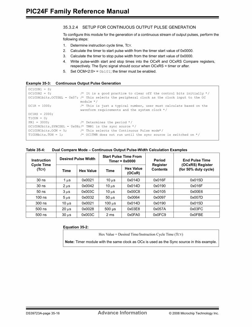
35.3.2.4 SETUP FOR CONTINUOUS OUTPUT PULSE GENERATION
To configure this module for the generation of a continuous stream of output pulses, perform thefollowing steps:
1. Determine instruction cycle time, TCY.2. Calculate the timer to start pulse width from the timer start value of 0x0000.3. Calculate the timer to stop pulse width from the timer start value of 0x0000.4. Write pulse-width start and stop times into the OCxR and OCxRS Compare registers,
respectively. The Sync signal should occur when OCxRS = timer or after.5. Set OCM<2:0> = 0b101; the timer must be enabled.
Example 35-3: Continuous Output Pulse Generation
Table 35-4: Dual Compare Mode � Continuous Output Pulse-Width Calculation Examples
Equation 35-2:
Instruction Cycle Time
(TCY)
Desired Pulse Width Start Pulse Time From Timer = 0x0000 Period
RegisterContents
End Pulse Time (OCxRS) Register
(for 50% duty cycle)Time Hex Value Time Hex Value(OCxR)
30 ns 1 μs 0x0021 10 μs 0x014D 0x016F 0x015D30 ns 2 μs 0x0042 10 μs 0x014D 0x0190 0x016F50 ns 3 μs 0x003C 10 μs 0x00C8 0x0105 0x00E6
100 ns 5 μs 0x0032 50 μs 0x0064 0x0097 0x007D300 ns 10 μs 0x0021 100 μs 0x014D 0x0190 0x015D500 ns 20 μs 0x0028 500 µs 0x03E8 0x057A 0x03FC500 ns 30 μs 0x003C 2 ms 0x0FA0 0x0FC9 0x0FBE
OC1CON1 = 0;OC1CON2 = 0; /* It is a good practice to clear off the control bits initially */OC1CON1bits.OCTSEL = 0x07; /* This selects the peripheral clock as the clock input to the OC
module */OC1R = 1000; /* This is just a typical number, user must calculate based on the
waveform requirements and the system clock */OC1RS = 2000;T1CON = 0;PR1 = 3000; /* Determines the period */OC1CON2bits.SYNCSEL = 0x0B;/* TMR1 is the sync source */OC1CON1bits.OCM = 5; /* This selects the Continuous Pulse mode*/T1CONbits.TON = 1; /* OC1TMR does not run until the sync source is switched on */
Hex Value = Desired Time/Instruction Cycle Time (TCY)
Note: Timer module with the same clock as OCx is used as the Sync source in this example.
DS39723A-page 35-16 Advance Information © 2008 Microchip Technology Inc.

Section 35. Output Compare with Dedicated TimerO
utputCompare
with
Dedicated Timer
35
Table 35-5: Special Cases for Dual Compare Match Mode Generating Continuous Output Pulse
Figure 35-11: Dual Compare Mode � Continuous Output Pulse (Sync Occurs When Timer = OCxRS)
Special Condition Operation Output
Synchronization occurs when the timer value is equal to OCxRS
Timer resets to zero in the next cycle, but the pulse is unaffected (see Figure 35-11).
Pulses
Synchronization occurs before the timer value reaches OCxR
Timer resets to zero before any output transition. Remains low
Synchronization occurs before the timer value reaches OCxRS but after it reaches OCxR
Only a single transition (low-to-high) is generated (see Figure 35-12).
Low-High
OCxR = OCxRS = 0x0000 and synchronization occurs
The output is initialized low and does not change. No interrupt is generated.
Remains low
OCxRS < OCxR The timer counts up to the first compare (TMRx = OCxR) and the first (rising) edge is generated. The timer then continues to count and eventually resets when synchronization occurs or rolls over. The timer then restarts from 0x0000 and counts up to the second compare (TMRx = OCxRS) and the second (falling) edge of the signal is generated. The falling edge of the output pulse generates an interrupt condition. The sequence repeats until the module is disabled.
Pulses
OCxR = OCxRS The timer counts up to the first compare (Timer = OCxR) and the first (rising) edge is generated. The timer continues to count and eventually resets when synchronization occurs or a rollover from FFFFh occurs. The timer then restarts from 0x0000 and counts up to the second compare (TMRx = OCxRS), and the second (falling) edge of the signal is generated. The falling edge of the output pulse generates an interrupt condition. The sequence repeats until the module is disabled.
Pulses
OCxR = 0x0000 and OCxRS > OCxR
The first cycle of the timer counts until synchronization occurs or rolls over; the output compare pin remains low. After the Timer reg-ister resets to zero, the output compare pin goes high. Upon the next timer match with the register, OCxRS, the output compare pin goes low and remains low. The falling edge of the output pulse generates an interrupt condition (see Figure 35-13). The sequence repeats until the module is disabled.
Pulses except for the first cycle
OCxIF
30033001 3002 3003 00003000OCxTMR 3002
Cleared by User
Note: In this example, one instruction clock period comprises 2 FOSC cycles.
1 Instruction Clock Period
2 TCY
3003
3000OCxR
3000
OCx pin
3003OCxRS
3001 30000000
2 TCY
OCx SyncOCxTMR Resets Here OCxTMR Resets Here
© 2008 Microchip Technology Inc. Advance Information DS39723A-page 35-17

PIC24F Family Reference Manual
Figure 35-12: Dual Compare Mode � Continuous Output Pulse (Sync Before Timer Reaches OCxRS)
Figure 35-13: Dual Compare Mode � Continuous Output Pulse (OCXR = 0X0000 (SYNCSEL<4:0> = 0X1F))
OCxIF
30033001 3002 3003 00003000OCxTMR 3002
Note: In this example, one instruction clock period comprises 2 FOSC cycles.
1 Instruction Clock Period
3003
3000
OCx Sync
OCxR
3000
OCx pin
3004OCxRS
3001 30000000OCxTMR Resets Here OCxTMR Resets Here
OCxRTime
Timer
OCxRS
OCxR = 0x0000
OCxM<2:0> = 0b101
(0x9000)
0
OCx pin
OCxIF
1 Timer Clock Period
OCxIF Cleared by User
DS39723A-page 35-18 Advance Information © 2008 Microchip Technology Inc.

Section 35. Output Compare with Dedicated TimerO
utputCompare
with
Dedicated Timer
35
35.3.3 Pulse-Width Modulation ModeWhen control bits, OCxCON1<OCM2:OCM0> = 0b110 or 0b111, then the PWM mode isselected. The registers, OCxR and OCxRS, are double-buffered in these modes. This means thatthe changes on these registers would be reflected only after a timer rollover from 0xFFFF or aftera Sync event occurs. As a result, any changes in these registers during operation occurs only withthe next pulse. Also, in these modes, Fault input is supported (described in the next sections).
35.3.3.1 EDGE-ALIGNED PWM MODEWhen control bits, OCM<2:0> = 0b110, the Edge-Aligned PWM mode of operation is selected.OCxR contains the current duty cycle and the SYNCSEL bits determine the period. OCxRS canbe made to determine the period by setting SYNCSEL<4:0> = 0x1F.
Figure 35-14 and Figure 35-15 illustrate the PWM mode operation.
Edge-Aligned PWM Mode Operation:
� When synchronization occurs, the following four events occur on the next increment cycle:- The timer is reset to zero and resumes counting- The OCx pin is set high (exception: if OCxRS = 0b0000, the OCx pin would not be set)- The OCxR and OCxRS Buffered registers are updated from OCxR and OCxRS- Interrupt flag, OCxIF, is set
� When the timer and OCxR match, the pin would be set low. This match does not generate interrupts.
Figure 35-14: PWM Output Timing
Figure 35-15: PWM Output Timing
Note: This is a migration issue for applications. In the old module, OCxRS is served as adouble-buffer to OCxR. In this version, both the registers are double-buffered.
Period
Duty Cycle
OCxTMR = OCxR
Load OCxRS Buffer with OCxRS
OCxTMR = 0
(Interrupt Flag)Load OCxR Buffer with OCxR
Set OCxIF = 1OCxTMR = OCxRSync Occurs
OCxIF
00010000 0001 0002 00030006OCxTMR 0000
Cleared by User
Note: In this example, one Instruction clock period comprises 2 FOSC cycles.
1 Instruction Clock Period
0006
0002
OCx Sync
OCxR
0005
OCx pin
0002OCxR
0006 00040002
Cleared by User
0004 0003
OCxR Buffer = (OCxR) OCxR Buffer = (OCxR)
0001Buffered New Duty Cycle Loaded Here
New Value Written to OCxRS
0001
© 2008 Microchip Technology Inc. Advance Information DS39723A-page 35-19
PIC24F Family Reference Manual
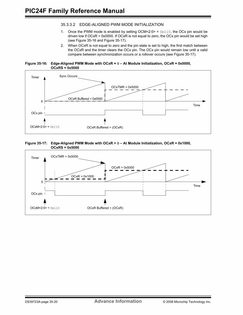
35.3.3.2 EDGE-ALIGNED PWM MODE INITIALIZATION
1. Once the PWM mode is enabled by setting OCM<2:0> = 0b110, the OCx pin would bedriven low if OCxR = 0x0000. If OCxR is not equal to zero, the OCx pin would be set high(see Figure 35-16 and Figure 35-17).
2. When OCxR is not equal to zero and the pin state is set to high, the first match betweenthe OCxR and the timer clears the OCx pin. The OCx pin would remain low until a validcompare between synchronization occurs or a rollover occurs (see Figure 35-17).
Figure 35-16: Edge-Aligned PWM Mode with OCxR = 0 � At Module Initialization, OCxR = 0x0000, OCxRS = 0x5000
Figure 35-17: Edge-Aligned PWM Mode with OCxR > 0 � At Module Initialization, OCxR = 0x1000, OCxRS = 0x5000
Time
Timer
OCxR Buffered = 0x0000
OCxM<2:0> = 0b110
0
OCx pin
OCxTMR = 0x5000
OCxR Buffered = (OCxR)
Sync Occurs
Time
Timer OCxTMR = 0x5000
OCxR = 0x1000
OCxM<2:0> = 0b110
0
OCx pin
OCxR = 0x5000
OCxR Buffered = (OCxR)
DS39723A-page 35-20 Advance Information © 2008 Microchip Technology Inc.

Section 35. Output Compare with Dedicated TimerO
utputCompare
with
Dedicated Timer
35
35.3.3.3 USER SETUP FOR PWM OPERATION
Perform the following steps while configuring the output compare module for the PWM operation:
1. Determine instruction cycle time, TCY.2. Calculate desired pulse on time value based upon TCY and write it into OCxR.3. Calculate the period value based upon TCY and write it into OCxRS.4. Write 0x1F to SYNCSEL<4:0> to select self Sync.5. Set the required clock source.6. Set OCM2:OCM0 of OCxCON1 = 0b110 to select Edge-Aligned PWM mode.
Example 35-4: PWM Mode
35.3.3.4 PWM MODE SPECIAL COMPARE CONDITIONS
Table 35-6 lists the PWM mode special compare conditions.
Table 35-6: Special Compare Mode Conditions
Figure 35-18: PWM Output Timing (0% Duty Cycle, OCxR = 0x0000)
OC1CON1 = 0; /* It is a good practice to clear off the control bits initially */OC1CON2 = 0;OC1CON1bits.OCTSEL = 0x07; /* This selects the peripheral clock as the clock input to the OC
module */OC1R = 1000; /* This is just a typical number, user must calculate based on the
waveform requirements and the system clock */OC1RS = 2000; /* Determines the Period */OC1CON1bits.OCM = 6; /* This selects the Edge Aligned PWM mode*/
Special Condition Operation Output
OCxR = 0 The OCx pin would be set low (see Figure 35-18). LowOCxR > OCxRS The OCx pin would be set high (see Figure 35-19). HighOCxR = OCxTMR and synchronization occurs
The OCx pin would remain high (see Figure 35-20). High
OCxIF
00000000 0001 0002 00030003TMR 0003
Cleared by User
Note: In this example, one instruction clock period comprises 2 FOSC cycles.
1 Instruction Clock Period
0003
0001
OCxRS
OCxR
0001
OCx pin
0001OCxR
0002 000300010000 0002
OCxR Buffer = (OCxR)
0000
0000
OCxR Buffer = (OCxR) OCxR Buffer = (OCxRS)Duty Cycle goes to 0%
Cleared by UserCleared by User
BufferedNew Duty Cycle Loaded Here
New Value Written to OCxR
© 2008 Microchip Technology Inc. Advance Information DS39723A-page 35-21

PIC24F Family Reference Manual
Figure 35-19: PWM Output Timing (100% Duty Cycle, OCxR > OCxRS (SYNCSEL<4:0> = 0x1F))
Figure 35-20: PWM Output Timing (OCxR = OCxRS (SYNCSEL<4:0> = 0x1F))
OCxIF
00000000 0001 0002 00030003TMR 0003
Cleared by User
Note: In this example, one instruction clock period comprises 2 FOSC cycles.
1 Instruction Clock Period
0003
0001
OCxRS
OCxR
0001
OCx pin
0001OCxR
0002 000300010000 0002
OCxR Buffer = (OCxR)
0004
0004
Duty Cycle goes to 100%
Cleared by UserCleared by User
Buffered
New Value Written to OCxR
New Duty Cycle loaded here
OCxIF
00000000 0001 0002 00030003TMR 0003
Cleared by User
Note: In this example, one Instruction clock period comprises 2 FOSC cycles.
1 Instruction Clock Period
0003
0001
OCxRS
OCxR
0001
OCx pin
0001OCxR
0002 000300010000 0002
0003
0003
OCxR Buffer = (OCxR)Duty Cycle goes to 100%
Cleared by UserCleared by User
Buffered
New Value Written to OCxR
New Duty Cycle Loaded Here
DS39723A-page 35-22 Advance Information © 2008 Microchip Technology Inc.

Section 35. Output Compare with Dedicated TimerO
utputCompare
with
Dedicated Timer
35
35.3.3.5 CENTER-ALIGNED PWM MODE
These mode (OCM<2:0> = 0b111) functions are the same as Continuous Pulse mode(OCM<2:0> = 0b101). The only differences are:
� OCxR and OCxRS are double-buffered, which means that the new register value would be effective only after a timer rollover or synchronization
� Fault control and pins are used
35.3.3.6 FAULT INPUT AND CONTROL
When operating in either the Center-Aligned PWM mode or Edge-aligned PWM mode(OCM<2:0> (OCxCON1<2:0>) = 0b111 or 0b110), the Fault pin and its controls can beactivated. Two Fault inputs, OCFA and OCFB, where OCFA controls OC1-OC4 and OCFBcontrols OC5-OC9, are available. The Fault pin is controlled by the register bit, ENFLT0(OCxCON1<15>). If this bit is zero, the corresponding Fault input pin (OCFA or OCFB) isignored. The status of the Fault input can be observed in the register bit, OCFLT0(OCxCON1<4>).
When a Fault occurs (OCFx = 0), the OCx pin output level is determined by the FLTOUT(OCxCON2<14>) bit. The tri-stating of the OCx pin during a Fault condition is controlled byFLTTRIEN (OCxCON2<13>).
The Fault control can operate in two modes based on the FLTMODE (OCxCON2<15>) bit:
� Inactive mode� Cycle-by-Cycle mode. Refer to the product data sheet for details on how Fault pins are
assigned to the various OCx peripherals.
35.3.3.6.1 Inactive ModeWhen FLTMODE (OCxCON2<15>) = 1, the Fault inputs operate in the Inactive mode (seeFigure 35-21). If the Fault input goes active (�0�), the OCFLT0 (OCxCON1<12>) bit would be setand the module would be in the Fault condition.
It remains in the Fault condition until:
� The Fault input goes inactive and� The OCFLT0 (OCxCON1<12>) bit is cleared in software and� A new timer cycle is started (timer goes to 0000h)
35.3.3.6.2 Cycle-by-Cycle ModeWhen FLTMODE (OCxCON2<15>) = 0, the Fault inputs operate in the Cycle-by-Cycle mode(see Figure 35-22). If a Fault input goes active (�0�), the OCFLT0 (OCxCON1<12>) bit would beset and the module would be in the Fault condition.
It remains in the Fault condition until:
� The Fault input goes inactive and� A new timer cycle is started (timer goes to 0x0000)
Note 1: Center alignment does not mean the pulse is exactly aligned to the center of thepulse width. It only indicates that the on time of the pulse can be positionedanywhere within the period.
Note: The Output Compare Fault pins, OCFA and OCFB, are active-low signals.
© 2008 Microchip Technology Inc. Advance Information DS39723A-page 35-23

PIC24F Family Reference Manual
Figure 35-21: Fault Input Pin Timing, Inactive Mode
Figure 35-22: Fault Input Pin Timing, Cycle-by-Cycle Mode
35.3.3.7 SYNCHRONOUS OPERATION
Synchronous operation of the timer is enabled when the OCTRIG (OCxCON2<7>) = 0.
In synchronous operation, the TRIGSTAT (OCxCON2<6>) bit has no function. The timer can besynchronized with the other modules using the synchronization/trigger inputs (seeRegister 35-2). Whenever the selected module receives a synchronization signal, the timerwould roll over to 0x0000 on the next positive edge of the selected clock.
35.3.3.8 USE OF THE MODULE TIMER IN A SYNCHRONIZED APPLICATION
Figure 35-23 illustrates the connections for synchronization and Figure 35-24 illustrates the tim-ing for multiple modules being synchronized. OC2 is being synchronized to OC1. Thesynchronization signal from OC1 is selected for synchronization by both OC1 and OC2 using theSYNCSEL<4:0>(OCxCON2<4:0>) bits. The OC1RS register now becomes the Period registerfor both OC1 and OC2.
When the OC1RS register matches the OC1 timer value, the OC1 module produces thesynchronization signal. This causes the timers in both OC1 and OC2 to go to zero on the nextpositive clock edge.
PWMOutput
OCFA/OCFB
OCFLT0 bit
DeletedPWM Pulse
Fault ConditionEnds OCFLT0 bit is Cleared
in Software
PWMOutput
OCFA/OCFB
OCFLT0 bit
DeletedPWM Pulse
Regions
OCFLT0 bit is Cleared Automaticallyat the End of each PWM Cycleunless the Fault is still Active
Note: Synchronized modules should select the same clock source to ensure proper function.
DS39723A-page 35-24 Advance Information © 2008 Microchip Technology Inc.

Section 35. Output Compare with Dedicated TimerO
utputCompare
with
Dedicated Timer
35
Figure 35-23: Synchronous Operation Integration (TRIGEN = 0)
Figure 35-24: Synchronous Operation
CLK
OC1
Sync In
CLK
OC2
Sync In
Sync Out
0012h
0010h 0011h 0012h 0000h 0001h 0002h
0010h 0011h 0012h 0000h 0001h 0002h
OC1
CLK
Sync Out from OC1
OC1RS
OC1TMR
Sync Out from OC1
CLK
Sync Out from OC1
OC2TMR
Note: The Sync out from OC1 is used as the input for OC1�s Sync in and OC2�s Sync in.
© 2008 Microchip Technology Inc. Advance Information DS39723A-page 35-25

PIC24F Family Reference Manual
When initializing synchronized modules, the module being used as the source of synchronizationshould be enabled last. As illustrated in Figure 35-23, OC2 should be initialized first and OC1should be initialized last. This ensures that the timers of all synchronized modules are maintainedin a Reset condition until the last module is initialized.
35.3.3.9 TRIGGER OPERATION
Trigger operation of the timer is enabled when OCTRIG (OCxCON2<7>) = 1. When configuredfor trigger operation, the module timer is held in Reset until a trigger event occurs. After thetrigger event occurs, the timer begins to count. The trigger source is selected by the SYNCSELbits.
35.3.3.10 OCxCON2 TRIGGER FUNCTION
The TRIGSTAT (OCxCON2<6>) bit holds the timer in Reset or releases it to count. It controls thetimer in the following manner:
� TRIGSTAT = 0- Timer is held in Reset
� TRIGSTAT = 1- Timer released from Reset- Timer increments on every positive clock
There are two types of trigger conditions when operating in Trigger mode:
� Hardware/software TRIGSTAT bit set� Software only TRIGSTAT bit set
In both cases, the trigger is always cleared in software.
35.3.3.10.1 Hardware/Software TRIGSTAT SetThe TRIGSTAT (OCxCON2<6>) bit can be set by hardware or software when:
� The SYNCSEL (OCxCON2<4:0>) bits are not equal to 0b00000 (see Section 35.3.3.12 �Illegal Settings�)
When the module is enabled for a triggered response, the timer would be held in a cleared state.It remains in this cleared state until a trigger event occurs, which sets the TRIGSTAT bit.Additionally, the timer can be released from Reset by writing to the TRIGSTAT bit and setting it.
35.3.3.10.2 Software Only TRIGSTAT SetThe TRIGSTAT bit can be set only by software when SYNCSEL<4:0> = 0b00000.
35.3.3.11 CLEARING TRIGSTAT BIT
The TRIGSTAT bit can only be cleared in software by writing a �0� to it. When the TRIGSTAT bitis cleared in software, the timer is reset to 0x0000 on the next timer clock�s rising edge and isready for another trigger.
35.3.3.12 ILLEGAL SETTINGS
It is illegal for the module to select itself as a trigger source. Therefore, two possible values of theSYNCSEL<4:0> in Trigger mode are not allowed:
� SYNCSEL<4:0> = 0x1F� SYNCSEL<4:0> = N, where N is the second setting that selects the same module (see
Register 35-2).
Note 1: TRIGSTAT cannot be changed in software when operating in One-Shot mode. SeeSection 35.3.3.13.2 �One-Shot Functionality� for more information on this mode.
2: The trigger source would be synchronized with the OCx clock.
3: Preventing these illegal conditions should be taken care of in the user software.
DS39723A-page 35-26 Advance Information © 2008 Microchip Technology Inc.

Section 35. Output Compare with Dedicated TimerO
utputCompare
with
Dedicated Timer
35
35.3.3.13 USE OF THE OCx MODULE IN A TRIGGERED APPLICATION
Figure 35-25 illustrates a typical application of the module timer in a triggered application. In thisapplication, a trigger event can be generated by another output compare module, timer module,IC module, analog comparator or other peripheral functions. Refer to the product data sheet fora complete list of trigger sources.
35.3.3.13.1 Initialization of the OCx Module in a Triggered ApplicationThe user misses any trigger event that occurs before the OCx module is initialized. Therefore, toavoid missing a trigger, it is recommended that the module be enabled before the trigger source.
Figure 35-25: Trigger Operation Integration (TRIGEN = 1)
35.3.3.13.2 One-Shot FunctionalityWhile operating as a trigger, the timer can operate in One-Shot mode. This produces one pulsefor every trigger. The One-Shot mode is enabled by setting the TRIGMODE (OCxCON1<3>) bit.In One-Shot mode, the timer remains in Reset until a trigger event occurs. This event sets theTRIGSTAT bit and the timer begins to count. When the timer rolls over to 0000h, the TRIGSTATbit would be cleared by the hardware if TRIGMODE = 1. This holds the timer in Reset until thenext trigger event, creating a one-shot timer.
35.3.4 Cascade ModeWhen 16-bit timers are not enough, the OCx modules can be grouped in pairs to cascade theminto 32-bit timers (see Figure 35-26). They are grouped as odd and even pairs (1-2, 3-4, 5-6,etc.). When cascading, the odd OCx module forms the Least Significant 16 bits of thetimer/compare and the even module forms the Most Significant 16 bits. The OCx pin of the evenmodule would be the output of the cascaded timers.
Figure 35-26: Cascade Operation
CLK
OC1
Sync/Trigger Out
Sync/Trigger In
CMP/TMR, etc.
Event/TriggerCLK
OC2 Outputand
Control Logic
OC1 Comp. OC1 Comp.
OC2 Comp. OC2 Comp.
OC1R OC2R
OC1RS OC1RS
OC2
OC1 CLK
LSB MSB
OC1TMR OC2TMR
© 2008 Microchip Technology Inc. Advance Information DS39723A-page 35-27

PIC24F Family Reference Manual
35.3.5 Setting Up Modules for CascadeIn this section, it is assumed that OC1 is the odd OC module and OC2 is the even.
The odd module is set up as follows:
� OC32 (OC1CON1<8>) = 1� OCTRIG (OC1CON2<7>) can either be �1� or �0� as the timer can either be synchronized or
triggered� OCTRIS (OC1CON2<5>) = 1 (since the OC1 pin would not be used, the output should be
tri-stated)
The even module is set up as follows:
� OC32 (OC2CON1<8>) = 1� OCTRIG (OC2CON2<7>) = 0 (even timer must be operated in Synchronized mode when
cascaded)� OCTRIS( OC2CON2<5>) = 0 (since OC2 would not be used, the output should be
enabled)
35.3.5.1 INITIALIZATION OF THE MODULES IN A CASCADE APPLICATION
When initializing cascaded modules, the even module should be initialized first and the oddmodule should be initialized last.
35.3.5.2 TIMER CLOCK SELECTION
This clock should be selected before the module is enabled, and should not be changed duringthe operation. The waveform for the cascade operation is illustrated in Figure 35-27.
Figure 35-27: Cascade Operation in Dual Compare Mode
Note: The even and odd OC modules must have the same clock.
0x0001
0x0002
0x0012
0x0012
0x0000 0x0001 0x0002 0x0001 0x0002
0x0012
CLK
OC1
OC1R
OC1RS
OC1TMR
OC2
OC2R
OC2RS
OC2TMR
OC2 pin
0x0001
0x0001
OC2IF
Cleared by User
DS39723A-page 35-28 Advance Information © 2008 Microchip Technology Inc.

Section 35. Output Compare with Dedicated TimerO
utputCompare
with
Dedicated Timer
35
35.3.5.3 CASCADE OPERATION WITH THE ODD MODULE TRIGGERED
When two modules are cascaded to form a 32-bit timer, the timer can be triggered by setting theodd module (OCTRIG = 1). The odd module remains in Reset until a trigger event occurs. Oncea trigger event occurs, the odd and even modules count as usual.
35.3.5.4 SYNCHRONIZING MULTIPLE CASCADED MODULE PAIRS
Multiple 32-bit pairs can also be synchronized, for example:
� To synchronize the OC3 + OC4 pair with the OC1 + OC2 pair:- OC1 and OC2 are set up as defined in Section 35.3.5 �Setting Up Modules for Cascade�- OC3 and OC4 are set up in the same way, but also SYNCSEL = 1 (synchronization out
from OC1); this allows the Sync out from OC1 to hold OC3 in Reset
Example 35-5: Output Compare in Cascade Mode
OC1CON1 = 0; /* It is a good practice to clear off the control bits initially */OC1CON2 = 0;OC2CON1 = 0;OC2CON2 = 0;
OC1CON1bits.OCTSEL = 0x07;/* This selects the peripheral clock as the clock input to the OC module */
OC2CON1bits.OCTSEL = 0x07;
OC1R = 0x1000; /* Determines the On-Time */ OC2R = 0x0002; /* Determines the On-Time */
OC1RS = 0x2000; /* Determines the Period */ OC2RS = 0x0003; /* Determines the Period */
OC1CON2bits.SYNCSEL = 0x1F;OC2CON2bits.SYNCSEL = 0x1F;
OC1CON2bits.OCTRIS = 1; /* Odd module's output is not required */
/* Even module must be enabled first *//* Odd module must be enabled last */
OC2CON2bits.OC32 = 1;OC1CON2bits.OC32 = 1;
OC2CON1bits.OCM = 6; /* This selects the Edge Aligned PWM mode */OC1CON1bits.OCM = 6;
© 2008 Microchip Technology Inc. Advance Information DS39723A-page 35-29

PIC24F Family Reference Manual
35.4 OUTPUT COMPARE OPERATION IN POWER-SAVING STATES
35.4.1 Output Compare Operation in Sleep ModeWhen the device enters Sleep mode, the system clock is disabled. During Sleep, the outputcompare channel drives the pin to the same active state as it was driven prior to entering theSleep state. The module then Halts at this state.
For example:
If the pin was high and the CPU enters the Sleep state, the pin stays high. Likewise, if the pinwas low and the CPU enters the Sleep state, the pin stays low. In both cases, when the deviceawakes, the output compare module resumes operation.
35.4.2 Sleep with PWM Fault Mode� When the module is in PWM Fault mode, the asynchronous portions of the Fault circuit
remain active. � If a Fault is detected, the output of OCx is determined by the FLTOUT and the OCTRIS
setting of OCxCON2 register. � The OCFLT0 bit would be set. An interrupt would not be generated at a Fault occurrence.
However, the interrupt would be queued and occurs at the time the part wakes up.
35.4.3 Output Compare Operation in Idle ModeWhen the device enters Idle mode, the system clock sources remain functional and the CPUstops executing code. The OCSIDL (OCxCON1<13>) bit selects if the output capture modulestops in Idle mode or continues operation in Idle mode.
� If OCSIDL = 1, the module discontinues the operation in Idle mode. The module performs the same procedures when stopped in the Idle mode (OCSIDL = 1) as it does for the Sleep mode.
� If OCSIDL = 0, the output compare channel(s) operate during the CPU Idle mode if the OCSIDL bit is a logic �0�. Furthermore, the time base must be enabled with the respective TSIDL bit set to a logic �0�; if internal, the timer is used as the clock source.
35.4.4 Doze ModeOutput compare operation in Doze mode is the same as in normal mode. When the device entersDoze mode, the system clock sources remain functional and the CPU may run at a slower clockrate.
35.4.5 Selective Peripheral Module ControlThe Peripheral Module Disable (PMD) registers provide a method to disable the output comparemodule by stopping all the clock sources supplied to it. When the module is disabled via theappropriate PMD control bit, it is in minimum power consumption state. The control and statusregisters associated with the module would also be disabled. Therefore, a write to these registerswould have no effect, and the read values would be invalid and return zero.
35.5 I/O PIN CONTROLWhen the output compare module is enabled, the I/O pin direction is controlled by the comparemodule. The compare module returns the I/O pin control back to the appropriate LAT and TRIScontrol bits when it is disabled. When the Simple PWM with Fault Protection Input mode isenabled, the OCFA/OCFB Fault pins must be configured as an input by setting the respectiveTRIS bit. Enabling this special PWM mode does not configure the OCFA/OCFB Fault pin as aninput.
Note: The external Fault pins, if enabled for use, continue to control the associated OCxoutput pins while the device is in Sleep or Idle mode.
Note: Refer to the product data sheet for available output compare pins.
DS39723A-page 35-30 Advance Information © 2008 Microchip Technology Inc.

Section 35. Output Compare with Dedicated TimerO
utput Compare w
ithDedicated Tim
er
35
35.6
REG
ISTE
R M
APS A s
umm
ary
of th
e re
gist
ers
asso
ciat
ed w
ith th
e P
IC24
F O
utpu
t Com
pare
with
Ded
icat
ed T
imer
mod
ule
is p
rovi
ded
in T
able
35-7
.
Tabl
e 35
-7:
Out
put C
ompa
re w
ith D
edic
ated
Tim
er R
egis
ter M
ap
File
Nam
eBi
t 15
Bit 1
4Bi
t 13
Bit 1
2Bi
t 11
Bit 1
0Bi
t 9Bi
t 8Bi
t 7Bi
t 6Bi
t 5Bi
t 4Bi
t 3Bi
t 2Bi
t 1Bi
t 0Al
l Re
sets
OC
xCO
N1
��
OC
SID
LO
CTS
EL2
OC
TSEL
1O
CTS
EL0
��
ENFL
T0�
�O
CFL
T0TR
IGM
OD
EO
CM
2O
CM
1O
CM
00000
OC
xCO
N2
FLTM
DFL
TOU
TFL
TTR
IEN
OC
INV
��
�O
C32
OC
TRIG
TRIG
STAT
OC
TRIS
SYN
CSE
L4SY
NC
SEL3
SYN
CSE
L2SY
NC
SEL1
SYN
CSE
L00000
OC
xRS
Out
put C
ompa
re x
Sec
onda
ry R
egist
er0000
OC
xRO
utpu
t Com
pare
x R
egist
er0000
OC
xTM
RTi
mer
Val
ue x
Reg
ister
xxxx
Lege
nd:
� =
uni
mpl
emen
ted,
read
as
�0�.
Res
et v
alue
s ar
e sh
own
in h
exad
ecim
al.
Not
e:Fo
r det
ails
on
the
Out
put C
ompa
re w
ith D
edic
ated
Tim
er m
ap, r
efer
to th
e sp
ecifi
c de
vice
dat
a sh
eet.
© 2008 Microchip Technology Inc. Advance Information DS39723A-page 35-31

PIC24F Family Reference Manual
35.7 ELECTRICAL SPECIFICATIONS
35.7.1 AC Characteristics
Figure 35-28: Output Compare Timings
Table 35-8: Output Capture
Figure 35-29: PWM Module Timing Requirements
Table 35-9: PWM Timing Requirements
Param. No. Symbol Characteristic Min Max Units Conditions
OC11 TCCR OC1 Output Rise Time � 10 ns �� � ns �
OC10 TCCF OC1 Output Fall Time � 10 ns �� � ns �
Param.No. Symbol Characteristic Min Typ(1) Max Units Conditions
OC15 TFD Fault Input to PWM I/O Change
� � 25 ns VDD = 3.0V, -40°C to +85°C
OC20 TFH Fault Input Pulse Width 50 � � ns VDD = 3.0V, -40°C to +85°CNote 1: Data in �Typ� column is at 3.3V, 25°C unless otherwise stated. These parameters are for design guidance
only and are not tested.
OCx
OC11 OC10(Output Compare or PWM Mode)
OCFx
PWM
OC20
OC15
DS39723A-page 35-32 Advance Information © 2008 Microchip Technology Inc.

Section 35. Output Compare with Dedicated TimerO
utputCompare
with
Dedicated Timer
35
35.8 DESIGN TIPS
Question 1: The output compare pin stops functioning even when the OCSIDL bit is notset. Why?
Answer: This is most likely to occur when the TSIDL (TxCON<13>) bit of the associated timersource is set if it is used as the clock source. Therefore, it is the timer that actually goes into theIdle mode when the PWRSAV instruction is executed and the clock is not generated.
Question 2: Can I cascade OC2 and OC3?Answer: No; cascading can be done only in pairs of OC1-OC2, OC3-OC4, etc., and OC9 cannotbe paired.
© 2008 Microchip Technology Inc. Advance Information DS39723A-page 35-33

PIC24F Family Reference Manual
35.9 RELATED APPLICATION NOTESThis section lists application notes that are related to this section of the manual. Theseapplication notes may not be written specifically for the PIC24F device family, but the conceptsare pertinent and could be used with modification and possible limitations. The currentapplication notes related to the Output Compare with Dedicated Timer module are:
Title Application Note #No related application notes at this time.
Note: Please visit the Microchip web site (www.microchip.com) for additional applicationnotes and code examples for the PIC24F family of devices.
DS39723A-page 35-34 Advance Information © 2008 Microchip Technology Inc.

Section 35. Output Compare with Dedicated TimerO
utputCompare
with
Dedicated Timer
35
35.10 REVISION HISTORYRevision A (February 2008)This is the initial released revision of this document.
© 2008 Microchip Technology Inc. Advance Information DS39723A-page 35-35

PIC24F Family Reference Manual
NOTES:
DS39723A-page 35-36 Advance Information © 2008 Microchip Technology Inc.


![Input / Output analysis - Babeș-Bolyai Universityper/Scs_Per/Sdv/C7_SdV.pdf · The International Input-Output Association[1] is dedicated to advance knowledge in the field input-output](https://img.pdfslide.net/doc/110x75/5d1f40d288c993364d8c7ea0/input-output-analysis-babe-bolyai-perscspersdvc7sdvpdf-the-international.jpg)