Embed Size (px)
Citation preview
Page 1 of 24 © 2020 Cornell Dubilier
Selecting and Applying DC Link Bus Capacitors for Inverter Applications
Sam G. Parler, Jr., P.E.
Cornell Dubilier
Abstract, aluminum electrolytic and DC film capacitors are widely used in all types of inverter
power systems, from variable-speed drives to welders, UPS systems and inverters for renewable
energy. This paper discusses the considerations involved in selecting the right type of bus
capacitors for such power systems, mainly in terms of ripple current handling and low-
impedance energy storage that maintains low ripple voltage. Examples of how to use Cornell
Dubilier’s web-based impedance modeling and lifetime modeling applets, whose calculation
inputs include not only ambient temperature and airflow velocities but also separate mains and
switching frequency components, are covered.
Introduction
In this paper, we will discuss how to go about choosing a capacitor technology (film or
electrolytic) and several of the capacitor parameters, such as nominal capacitance, rated ripple
current, and temperature, for power inverter applications of a few hundred watts and up.
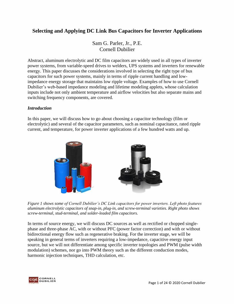
Figure 1 shows some of Cornell Dubilier’s DC Link capacitors for power inverters. Left photo features
aluminum electrolytic capacitors of snap-in, plug-in, and screw-terminal varieties. Right photo shows
screw-terminal, stud-terminal, and solder-leaded film capacitors.
In terms of source energy, we will discuss DC sources as well as rectified or chopped single-
phase and three-phase AC, with or without PFC (power factor correction) and with or without
bidirectional energy flow such as regenerative braking. For the inverter stage, we will be
speaking in general terms of inverters requiring a low-impedance, capacitive energy input
source, but we will not differentiate among specific inverter topologies and PWM (pulse width
modulation) schemes, nor go into PWM theory such as the different conduction modes,
harmonic injection techniques, THD calculation, etc.
Page 2 of 24 © 2020 Cornell Dubilier
Review of the basic power conversion scheme
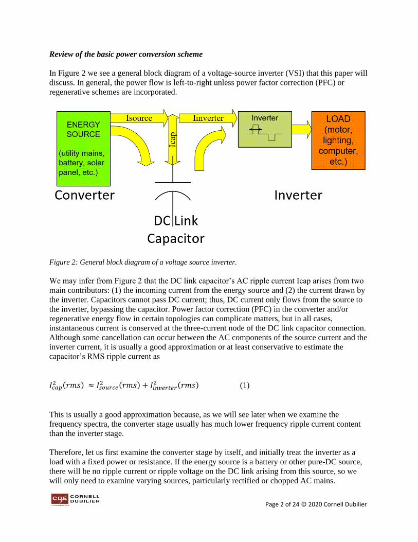
In Figure 2 we see a general block diagram of a voltage-source inverter (VSI) that this paper will
discuss. In general, the power flow is left-to-right unless power factor correction (PFC) or
regenerative schemes are incorporated.
Figure 2: General block diagram of a voltage source inverter.
We may infer from Figure 2 that the DC link capacitor’s AC ripple current Icap arises from two
main contributors: (1) the incoming current from the energy source and (2) the current drawn by
the inverter. Capacitors cannot pass DC current; thus, DC current only flows from the source to
the inverter, bypassing the capacitor. Power factor correction (PFC) in the converter and/or
regenerative energy flow in certain topologies can complicate matters, but in all cases,
instantaneous current is conserved at the three-current node of the DC link capacitor connection.
Although some cancellation can occur between the AC components of the source current and the
inverter current, it is usually a good approximation or at least conservative to estimate the
capacitor’s RMS ripple current as
𝐼𝑐𝑎𝑝2 (𝑟𝑚𝑠) ≈ 𝐼𝑠𝑜𝑢𝑟𝑐𝑒
2 (𝑟𝑚𝑠) + 𝐼𝑖𝑛𝑣𝑒𝑟𝑡𝑒𝑟2 (𝑟𝑚𝑠) (1)
This is usually a good approximation because, as we will see later when we examine the
frequency spectra, the converter stage usually has much lower frequency ripple current content
than the inverter stage.
Therefore, let us first examine the converter stage by itself, and initially treat the inverter as a
load with a fixed power or resistance. If the energy source is a battery or other pure-DC source,
there will be no ripple current or ripple voltage on the DC link arising from this source, so we
will only need to examine varying sources, particularly rectified or chopped AC mains.
Page 3 of 24 © 2020 Cornell Dubilier
Analysis of Energy Source Contributions to
DC Link Ripple Current and Ripple Voltage
To facilitate the analysis and make the conclusions as general as possible, let us implement Per-
Unit (PU) analysis based on the load power drawn by the inverter, assuming a conserved
quantity Power and a mains frequency f. This basis is therefore equal to the ideal DC power
delivered to a load resistor, so the base voltage is equal to the peak voltage at zero ripple voltage.
𝑉𝑏𝑎𝑠𝑒 = 𝑉𝑑𝑐(𝑃𝑒𝑎𝑘)
𝐼𝑏𝑎𝑠𝑒 =𝑃𝑜𝑤𝑒𝑟
𝑉𝑏𝑎𝑠𝑒
𝑅𝑏𝑎𝑠𝑒 =𝑉𝑏𝑎𝑠𝑒
2
𝑃𝑜𝑤𝑒𝑟
𝐿𝑏𝑎𝑠𝑒 =𝑉𝑏𝑎𝑠𝑒
2
2𝜋𝑓𝑃𝑜𝑤𝑒𝑟
𝐶𝑏𝑎𝑠𝑒 =𝑃𝑜𝑤𝑒𝑟
2𝜋𝑓𝑉𝑏𝑎𝑠𝑒2
Let us first examine rectified single-phase 50 Hz mains with ideal diodes. Such “linear” power
supply schemes can produce very high ripple current in the DC link capacitor, as it serves as a
filter capacitor in this role. The current pulses charging the capacitor when the diode(s) are
forward-biased are generally much briefer than the time the capacitor is discharging into the
load. Due to the principle of Charge Conservation in a capacitor, these pulses are therefore quite
a bit higher in amplitude than the load current. This usually results in the capacitor’s RMS ripple
current being greater than the DC current delivered to the load. Generally, some amount of line
inductance is added, or transformer leakage inductance is considered or recognized, for valid
modeling and/or implementation.
Figure 3 shows a full-wave bridge schematic which we will first analyze on a per-unit basis for
the capacitor’s AC RMS ripple current and peak-to-peak ripple voltage.
Most power supply designers want a peak-to-peak ripple voltage of less than 5%, and usually
limit line inductance to about 5% per-unit. What we see from the Spice analysis results
summarized in Figure 4 is that of a single-phase full-wave bridge analysis of the circuit of Figure
3. In order to accomplish these objectives, a lot of capacitance is needed, on the order of 40 PU
or more. Figure 5 shows that as long as some line inductance such as 1% per-unit is
incorporated, the RMS ripple current isn’t very sensitive to the level of capacitance. In Figure 6
we show the frequency content of the capacitor ripple current. Nearly zero at DC (0 Hz) as it
should be, then only a few components at 2, 4, and 6 times the line frequency.

Page 4 of 24 © 2020 Cornell Dubilier
Figure 3: Full-wave bridge with line inductor, filter capacitor, and resistive load.
Figure 4: Per-unit analysis of percent peak-to-peak ripple voltage versus line inductance for four values
of filter capacitance.
L1 1 *
V
+
VM1
C1
D4
D3
D2
D1
R1A
+
AM1
+
VG1

Page 5 of 24 © 2020 Cornell Dubilier
Figure 5: Per-unit analysis of RMS ripple current through the filter capacitor versus line inductance for
four values of filter capacitance.
Figure 6: Ripple current magnitude frequency spectrum for a full-wave bridge with 50 Hz mains.
The abscissas are multiples of 12.5 Hz, and thus the energy bands are at all even-integer
multiples of the mains frequency, decaying rapidly.
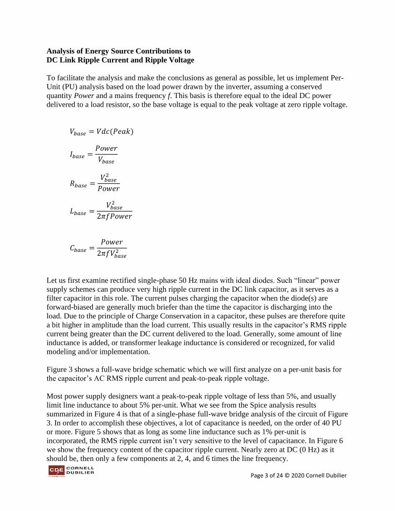
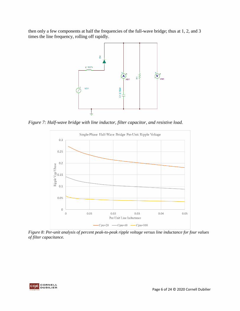
Figure 7 shows a half-wave bridge schematic, which is even more demanding on a per-unit basis
than was the full-wave bridge, as far as the capacitor’s AC RMS ripple current and peak-to-peak
ripple voltage are concerned. The analysis summarized in Figure 8 shows that to achieve a peak-to-
peak ripple voltage of less than 5%, a capacitance on the order of 100 PU or more is required. It’s
probably cheaper to just add three diodes! Figure 9 shows that more line inductance such as several
percent per-unit is needed to lower the RMS ripple current to a modest level. In Figure 10 we see
that the frequency content of the capacitor ripple current is nearly zero at DC (0 Hz) as it must be,
Page 6 of 24 © 2020 Cornell Dubilier
then only a few components at half the frequencies of the full-wave bridge; thus at 1, 2, and 3
times the line frequency, rolling off rapidly.
Figure 7: Half-wave bridge with line inductor, filter capacitor, and resistive load.
Figure 8: Per-unit analysis of percent peak-to-peak ripple voltage versus line inductance for four values
of filter capacitance.

Page 7 of 24 © 2020 Cornell Dubilier
Figure 9: Per-unit analysis of RMS ripple current through the filter capacitor versus line inductance for
four values of filter capacitance.
Figure 10: Ripple current magnitude frequency spectrum for a half-wave bridge with 50 Hz mains. The
abscissas are multiples of 12.5 Hz, and thus the energy bands are at all integer multiples of the mains
frequency, decaying rapidly.
Next, we move on in our converter-stage analysis from single-phase rectifiers to three-phase, six-
diode rectifiers, very common input for our DC Link film and electrolytic capacitors. See Figure
11. The per-unit inductance is in each leg of the three-phase lines. We are going to keep the same
base units as for single phase so that the comparisons will be on the nominal power delivered to
the resistive load at its nominal peak voltage. Such rectified mains configuration without L and C
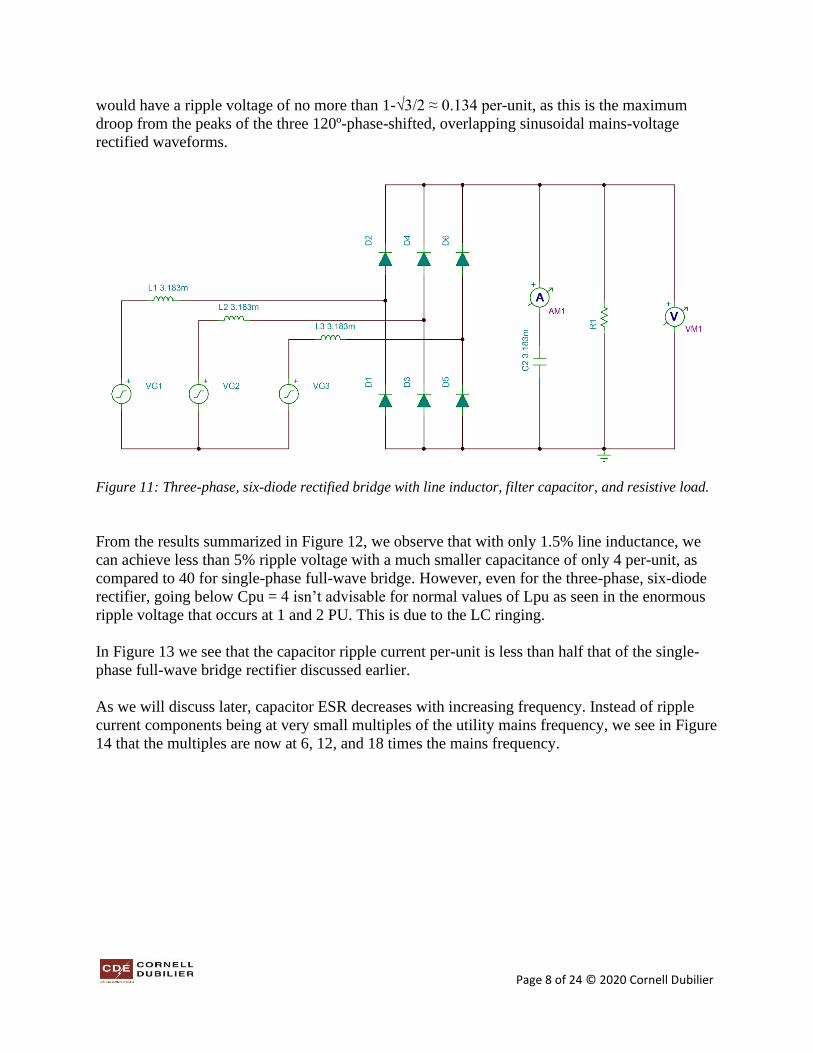
Page 8 of 24 © 2020 Cornell Dubilier
would have a ripple voltage of no more than 1-√3/2 ≈ 0.134 per-unit, as this is the maximum
droop from the peaks of the three 120º-phase-shifted, overlapping sinusoidal mains-voltage
rectified waveforms.
Figure 11: Three-phase, six-diode rectified bridge with line inductor, filter capacitor, and resistive load.
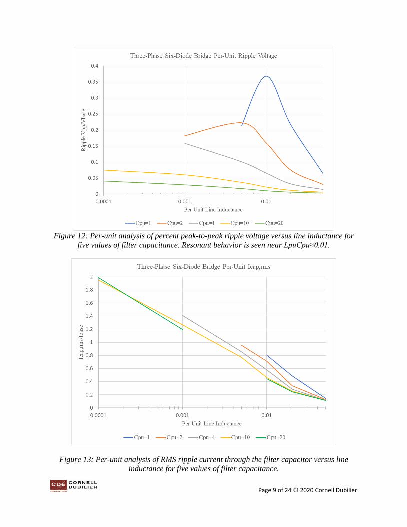
From the results summarized in Figure 12, we observe that with only 1.5% line inductance, we
can achieve less than 5% ripple voltage with a much smaller capacitance of only 4 per-unit, as
compared to 40 for single-phase full-wave bridge. However, even for the three-phase, six-diode
rectifier, going below Cpu = 4 isn’t advisable for normal values of Lpu as seen in the enormous
ripple voltage that occurs at 1 and 2 PU. This is due to the LC ringing.
In Figure 13 we see that the capacitor ripple current per-unit is less than half that of the single-
phase full-wave bridge rectifier discussed earlier.
As we will discuss later, capacitor ESR decreases with increasing frequency. Instead of ripple
current components being at very small multiples of the utility mains frequency, we see in Figure
14 that the multiples are now at 6, 12, and 18 times the mains frequency.
Page 9 of 24 © 2020 Cornell Dubilier
Figure 12: Per-unit analysis of percent peak-to-peak ripple voltage versus line inductance for
five values of filter capacitance. Resonant behavior is seen near LpuCpu≈0.01.
Figure 13: Per-unit analysis of RMS ripple current through the filter capacitor versus line
inductance for five values of filter capacitance.
Page 10 of 24 © 2020 Cornell Dubilier
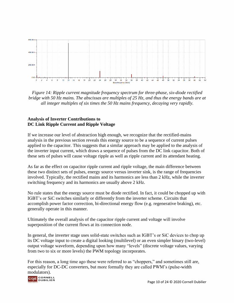
Figure 14: Ripple current magnitude frequency spectrum for three-phase, six-diode rectified
bridge with 50 Hz mains. The abscissas are multiples of 25 Hz, and thus the energy bands are at
all integer multiples of six times the 50 Hz mains frequency, decaying very rapidly.
Analysis of Inverter Contributions to
DC Link Ripple Current and Ripple Voltage
If we increase our level of abstraction high enough, we recognize that the rectified-mains
analysis in the previous section reveals this energy source to be a sequence of current pulses
applied to the capacitor. This suggests that a similar approach may be applied to the analysis of
the inverter input current, which draws a sequence of pulses from the DC link capacitor. Both of
these sets of pulses will cause voltage ripple as well as ripple current and its attendant heating.
As far as the effect on capacitor ripple current and ripple voltage, the main difference between
these two distinct sets of pulses, energy source versus inverter sink, is the range of frequencies
involved. Typically, the rectified mains and its harmonics are less than 2 kHz, while the inverter
switching frequency and its harmonics are usually above 2 kHz.
No rule states that the energy source must be diode rectified. In fact, it could be chopped up with
IGBT’s or SiC switches similarly or differently from the inverter scheme. Circuits that
accomplish power factor correction, bi-directional energy flow (e.g. regenerative braking), etc.
generally operate in this manner.
Ultimately the overall analysis of the capacitor ripple current and voltage will involve
superposition of the current flows at its connection node.
In general, the inverter stage uses solid-state switches such as IGBT’s or SiC devices to chop up
its DC voltage input to create a digital looking (multilevel) or an even simpler binary (two-level)
output voltage waveform, depending upon how many “levels” (discrete voltage values, varying
from two to six or more levels) the PWM topology incorporates.
For this reason, a long time ago these were referred to as “choppers,” and sometimes still are,
especially for DC-DC converters, but more formally they are called PWM’s (pulse-width
modulators).
Page 11 of 24 © 2020 Cornell Dubilier
The unfiltered PWM output voltage is never a true sine wave, but when driving an inductive
load such as a motor, the current will tend to be proportional to the time-integral of the PWM
voltage waveform, whose modulation scheme is designed so that the webers (volt-seconds) of
these pulses will produce approximately a sinusoidal current, since for an inductor L, we have a
current i = ∫ v dt/L. And for applications such as a UPS, requiring something close to a sinusoidal
voltage, an LC or ferro-resonant filter can be used after the PWM stage, effectively integrating
and low-pass-filtering the voltage waveform.
As will be discussed later, the PWM control/modulation scheme can affect capacitor heating, but
usually, the primary goals of the power supply designer are to meet (1) efficiency goals, (2)
overall cost, size, and reliability constraints and (3) total harmonic distortion limits such as 5%,
and sometimes input power factor limits. So minimizing capacitor losses isn’t always the highest
priority for the power supply design engineer. Still, it is good to investigate and quantify the
relative impact of various factors affecting the capacitor stress.
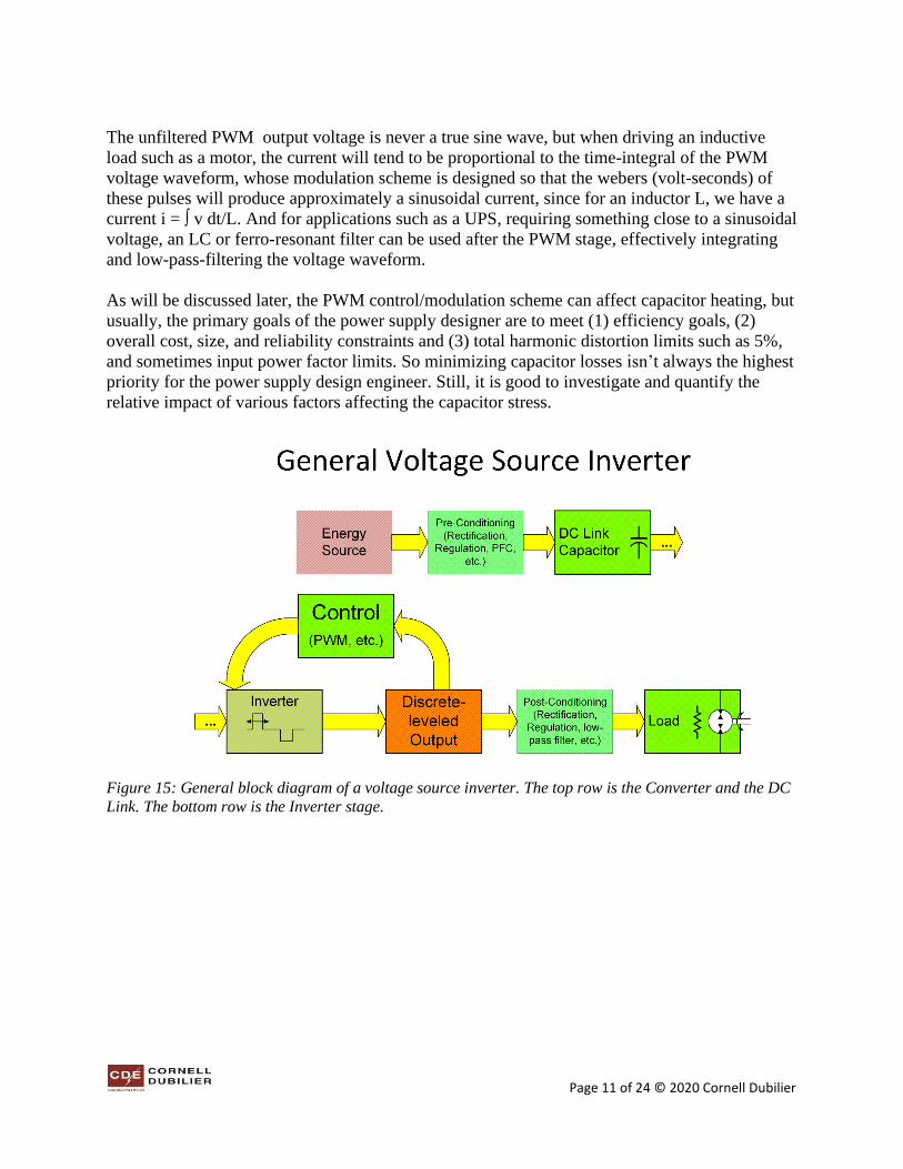
Figure 15: General block diagram of a voltage source inverter. The top row is the Converter and the DC
Link. The bottom row is the Inverter stage.

Page 12 of 24 © 2020 Cornell Dubilier
Figure 16: Three example application topologies. The topological variations arise from differences in the
nature of the energy supply and demand.
Page 13 of 24 © 2020 Cornell Dubilier
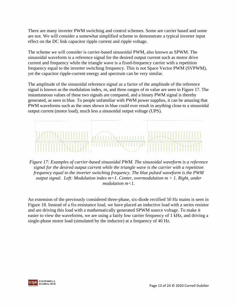
There are many inverter PWM switching and control schemes. Some are carrier based and some
are not. We will consider a somewhat simplified scheme to demonstrate a typical inverter input
effect on the DC link capacitor ripple current and ripple voltage.
The scheme we will consider is carrier-based sinusoidal PWM, also known as SPWM. The
sinusoidal waveform is a reference signal for the desired output current such as motor drive
current and frequency while the triangle wave is a fixed-frequency carrier with a repetition
frequency equal to the inverter switching frequency. This is not Space Vector PWM (SVPWM),
yet the capacitor ripple-current energy and spectrum can be very similar.
The amplitude of the sinusoidal reference signal as a factor of the amplitude of the reference
signal is known as the modulation index, m, and three ranges of m value are seen in Figure 17. The
instantaneous values of these two signals are compared, and a binary PWM signal is thereby
generated, as seen in blue. To people unfamiliar with PWM power supplies, it can be amazing that
PWM waveforms such as the ones shown in blue could ever result in anything close to a sinusoidal
output current (motor load), much less a sinusoidal output voltage (UPS).
Figure 17: Examples of carrier-based sinusoidal PWM. The sinusoidal waveform is a reference
signal for the desired output current while the triangle wave is the carrier with a repetition
frequency equal to the inverter switching frequency. The blue pulsed waveform is the PWM
output signal. Left: Modulation index m=1. Center, overmodulation m > 1. Right, under
modulation m<1.
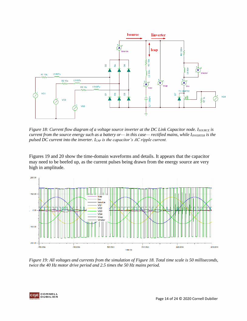
An extension of the previously considered three-phase, six-diode rectified 50 Hz mains is seen in
Figure 18. Instead of a fix-resistance load, we have placed an inductive load with a series resistor
and are driving this load with a mathematically generated SPWM source voltage. To make it
easier to view the waveforms, we are using a fairly low carrier frequency of 1 kHz, and driving a
single-phase motor load (simulated by the inductor) at a frequency of 40 Hz.
Page 14 of 24 © 2020 Cornell Dubilier
Figure 18: Current flow diagram of a voltage source inverter at the DC Link Capacitor node. ISOURCE is
current from the source energy such as a battery or— in this case— rectified mains, while IINVERTER is the
pulsed DC current into the inverter. ICAP is the capacitor’s AC ripple current.
Figures 19 and 20 show the time-domain waveforms and details. It appears that the capacitor
may need to be beefed up, as the current pulses being drawn from the energy source are very
high in amplitude.
Figure 19: All voltages and currents from the simulation of Figure 18. Total time scale is 50 milliseconds,
twice the 40 Hz motor drive period and 2.5 times the 50 Hz mains period.
Page 15 of 24 © 2020 Cornell Dubilier
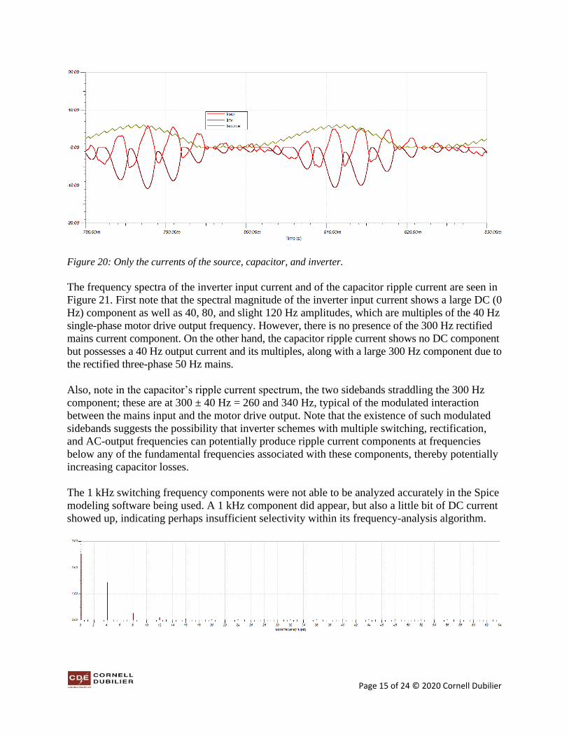
Figure 20: Only the currents of the source, capacitor, and inverter.
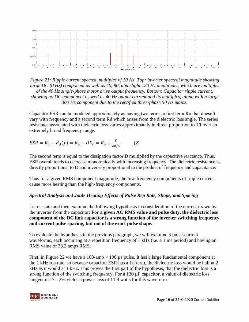
The frequency spectra of the inverter input current and of the capacitor ripple current are seen in
Figure 21. First note that the spectral magnitude of the inverter input current shows a large DC (0
Hz) component as well as 40, 80, and slight 120 Hz amplitudes, which are multiples of the 40 Hz
single-phase motor drive output frequency. However, there is no presence of the 300 Hz rectified
mains current component. On the other hand, the capacitor ripple current shows no DC component
but possesses a 40 Hz output current and its multiples, along with a large 300 Hz component due to
the rectified three-phase 50 Hz mains.
Also, note in the capacitor’s ripple current spectrum, the two sidebands straddling the 300 Hz
component; these are at 300 ± 40 Hz = 260 and 340 Hz, typical of the modulated interaction
between the mains input and the motor drive output. Note that the existence of such modulated
sidebands suggests the possibility that inverter schemes with multiple switching, rectification,
and AC-output frequencies can potentially produce ripple current components at frequencies
below any of the fundamental frequencies associated with these components, thereby potentially
increasing capacitor losses.
The 1 kHz switching frequency components were not able to be analyzed accurately in the Spice
modeling software being used. A 1 kHz component did appear, but also a little bit of DC current
showed up, indicating perhaps insufficient selectivity within its frequency-analysis algorithm.
Page 16 of 24 © 2020 Cornell Dubilier
Figure 21: Ripple current spectra, multiples of 10 Hz. Top: inverter spectral magnitude showing
large DC (0 Hz) component as well as 40, 80, and slight 120 Hz amplitudes, which are multiples
of the 40 Hz single-phase motor drive output frequency. Bottom: Capacitor ripple current,
showing no DC component as well as 40 Hz output current and its multiples, along with a large
300 Hz component due to the rectified three-phase 50 Hz mains.
Capacitor ESR can be modeled approximately as having two terms, a first term Ro that doesn’t
vary with frequency and a second term Rd which arises from the dielectric loss angle. The series
resistance associated with dielectric loss varies approximately in direct proportion to 1/f over an
extremely broad frequency range.
𝐸𝑆𝑅 = 𝑅𝑜 + 𝑅𝑑(𝑓) = 𝑅𝑜 + 𝐷𝑋𝑐 = 𝑅𝑜 +𝐷
2𝜋𝑓𝐶 (2)
The second term is equal to the dissipation factor D multiplied by the capacitive reactance. Thus,
ESR overall tends to decrease monotonically with increasing frequency. The dielectric resistance is
directly proportional to D and inversely proportional to the product of frequency and capacitance.
Thus for a given RMS component magnitude, the low-frequency components of ripple current
cause more heating than the high-frequency components.
Spectral Analysis and Joule Heating Effects of Pulse Rep Rate, Shape, and Spacing
Let us state and then examine the following hypothesis in consideration of the current drawn by
the inverter from the capacitor: For a given AC RMS value and pulse duty, the dielectric loss
component of the DC link capacitor is a strong function of the inverter switching frequency
and current pulse spacing, but not of the exact pulse shape.
To evaluate the hypothesis in the previous paragraph, we will examine 5 pulse-current
waveforms, each occurring at a repetition frequency of 1 kHz (i.e. a 1 ms period) and having an
RMS value of 33.3 amps RMS.
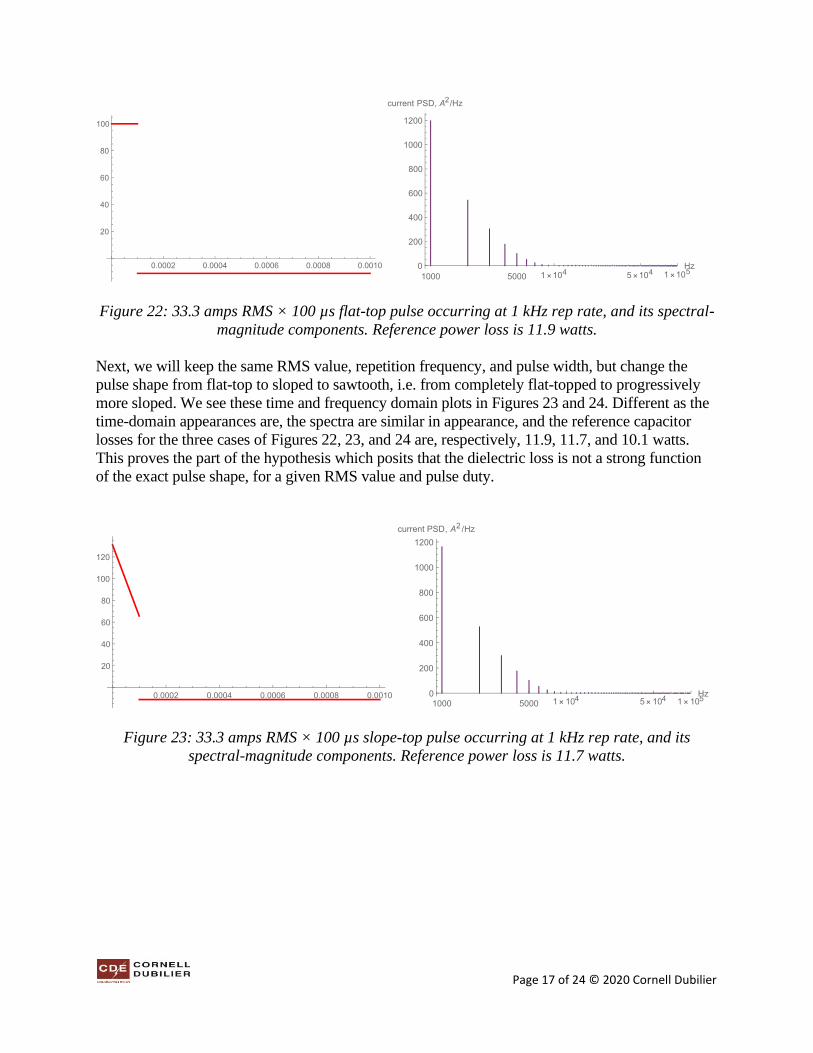
First, in Figure 22 we have a 100-amp × 100 µs pulse. It has a large fundamental component at
the 1 kHz rep rate, so because capacitor ESR has a 1/f term, the dielectric loss would be half at 2
kHz as it would at 1 kHz. This proves the first part of the hypothesis, that the dielectric loss is a
strong function of the switching frequency. For a 130 µF capacitor, a value of dielectric loss
tangent of D = 2% yields a power loss of 11.9 watts for this waveform.
Page 17 of 24 © 2020 Cornell Dubilier
Figure 22: 33.3 amps RMS × 100 µs flat-top pulse occurring at 1 kHz rep rate, and its spectral-
magnitude components. Reference power loss is 11.9 watts.
Next, we will keep the same RMS value, repetition frequency, and pulse width, but change the
pulse shape from flat-top to sloped to sawtooth, i.e. from completely flat-topped to progressively
more sloped. We see these time and frequency domain plots in Figures 23 and 24. Different as the
time-domain appearances are, the spectra are similar in appearance, and the reference capacitor
losses for the three cases of Figures 22, 23, and 24 are, respectively, 11.9, 11.7, and 10.1 watts.
This proves the part of the hypothesis which posits that the dielectric loss is not a strong function
of the exact pulse shape, for a given RMS value and pulse duty.
Figure 23: 33.3 amps RMS × 100 µs slope-top pulse occurring at 1 kHz rep rate, and its
spectral-magnitude components. Reference power loss is 11.7 watts.
Page 18 of 24 © 2020 Cornell Dubilier
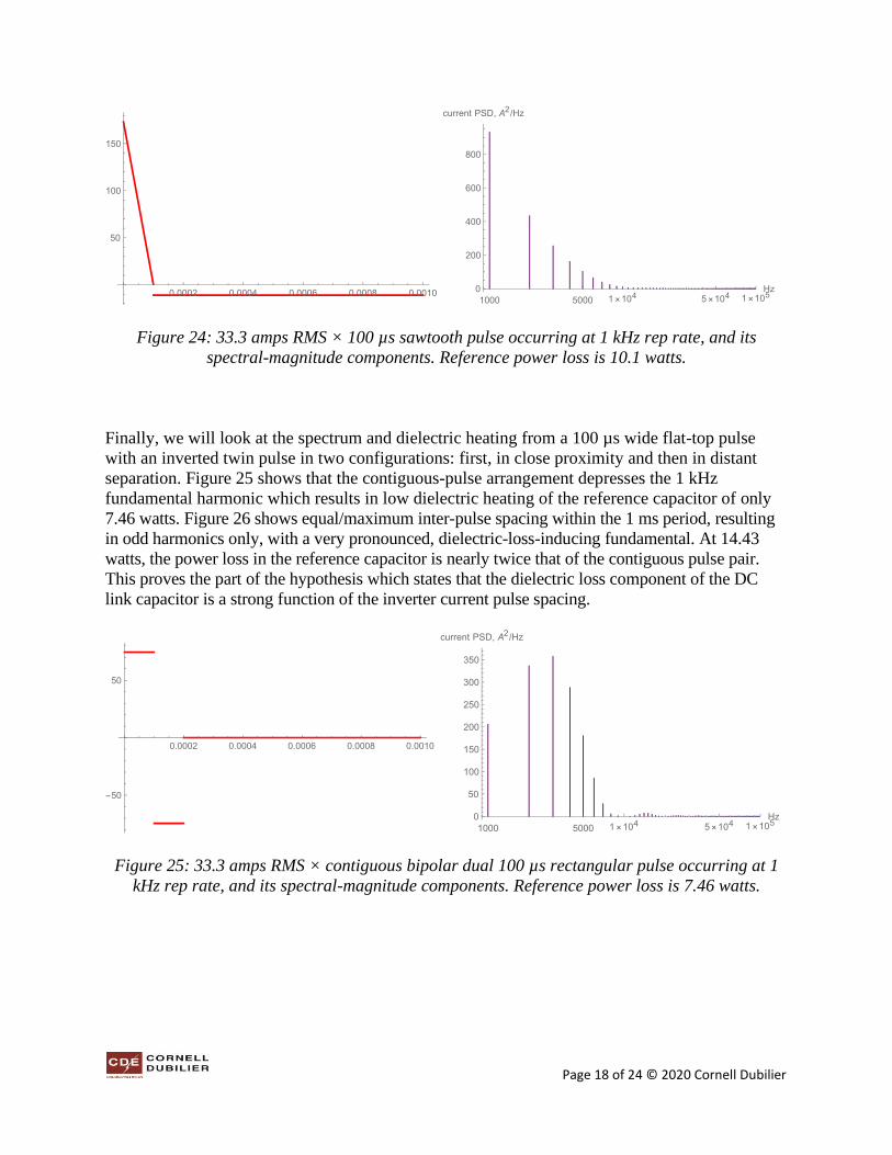
Figure 24: 33.3 amps RMS × 100 µs sawtooth pulse occurring at 1 kHz rep rate, and its
spectral-magnitude components. Reference power loss is 10.1 watts.
Finally, we will look at the spectrum and dielectric heating from a 100 µs wide flat-top pulse
with an inverted twin pulse in two configurations: first, in close proximity and then in distant
separation. Figure 25 shows that the contiguous-pulse arrangement depresses the 1 kHz
fundamental harmonic which results in low dielectric heating of the reference capacitor of only
7.46 watts. Figure 26 shows equal/maximum inter-pulse spacing within the 1 ms period, resulting
in odd harmonics only, with a very pronounced, dielectric-loss-inducing fundamental. At 14.43
watts, the power loss in the reference capacitor is nearly twice that of the contiguous pulse pair.
This proves the part of the hypothesis which states that the dielectric loss component of the DC
link capacitor is a strong function of the inverter current pulse spacing.
Figure 25: 33.3 amps RMS × contiguous bipolar dual 100 µs rectangular pulse occurring at 1
kHz rep rate, and its spectral-magnitude components. Reference power loss is 7.46 watts.

Page 19 of 24 © 2020 Cornell Dubilier
Figure 26: 33.3 amps RMS, maximally-separated bipolar dual 100 µs rectangular pulse occurring
at 1 kHz rep rate, and its spectral-magnitude components. Reference power loss is 14.43 watts,
nearly twice the power loss of the same pulses when contiguous as in the previous figure.
General expression for DC Link ripple current for
PWM inverter with balanced 3-phase output
For the case of a PWM inverter with balanced 3-phase output, there is an expression that gives a
good estimate of the capacitor ripple current in terms of the previously discussed modulation
index m as well as the load’s phase current, and is generally accurate within several percent for
most PWM inverter modulation schemes with three-phase AC outputs. This expression is
attributed to Kolar et al and is equation (3) below. Note that it is the ratio of the capacitor RMS
current to the line output current from the inverter to the load. Note also that it is independent of
the inverter switching frequency.
𝐼𝐶𝐴𝑃 , 𝑟𝑚𝑠 ≡ 𝐼𝐿 , 𝑟𝑚𝑠 √2𝑚 [√3
4𝜋+ (
√3
𝜋−
9𝑚
16) 𝑐𝑜𝑠2(𝜑)] (3)
This expression is graphed in Figure 27 for a wide range of modulation indexes and load phase
angles.
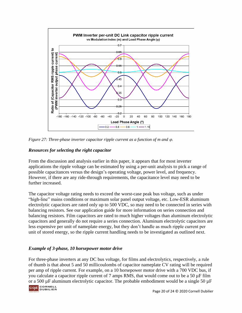
Page 20 of 24 © 2020 Cornell Dubilier
Figure 27: Three-phase inverter capacitor ripple current as a function of m and .
Resources for selecting the right capacitor
From the discussion and analysis earlier in this paper, it appears that for most inverter
applications the ripple voltage can be estimated by using a per-unit analysis to pick a range of
possible capacitances versus the design’s operating voltage, power level, and frequency.
However, if there are any ride-through requirements, the capacitance level may need to be
further increased.
The capacitor voltage rating needs to exceed the worst-case peak bus voltage, such as under
“high-line” mains conditions or maximum solar panel output voltage, etc. Low-ESR aluminum
electrolytic capacitors are rated only up to 500 VDC, so may need to be connected in series with
balancing resistors. See our application guide for more information on series connection and
balancing resistors. Film capacitors are rated to much higher voltages than aluminum electrolytic
capacitors and generally do not require a series connection. Aluminum electrolytic capacitors are
less expensive per unit of nameplate energy, but they don’t handle as much ripple current per
unit of stored energy, so the ripple current handling needs to be investigated as outlined next.
Example of 3-phase, 10 horsepower motor drive
For three-phase inverters at any DC bus voltage, for films and electrolytics, respectively, a rule
of thumb is that about 5 and 50 millicoulombs of capacitor nameplate CV rating will be required
per amp of ripple current. For example, on a 10 horsepower motor drive with a 700 VDC bus, if
you calculate a capacitor ripple current of 7 amps RMS, that would come out to be a 50 µF film
or a 500 µF aluminum electrolytic capacitor. The probable embodiment would be a single 50 µF
Page 21 of 24 © 2020 Cornell Dubilier
800 VDC film vs two 1,000 µF 400V aluminum electrolytic capacitors in series. For single-
phase or high-impedance input, or large ride-through requirements, these rules of thumb may
need to be tripled or more.
If we want to examine the per-unit capacitance of the above, we can rearrange our earlier base
equations, but we shouldn’t use the capacitor voltage and ripple current but rather the motor line
voltage and full-load current. Let us suppose that the 10 HP motor is driven with 460V and 12.4
amps. Using a three-phase base power of √3VLINEILINE = 9880 VA results in per-unit capacitance
values of Cpu=3.36 for the electrolytic and 0.336 for the film.
Since capacitor lifetime and failure rate are exponential functions of temperature and thus of
ripple current, the ripple current stress on the DC link capacitor is critical and needs to be managed
carefully and conservatively. Assuming that the minimum capacitance and voltage rating have
been chosen as discussed above, the best way to proceed in selecting candidate capacitors is based
upon ripple current handling. So the first step is to calculate the total ripple current.
A rule of thumb regarding ripple current handling is to choose a capacitor whose rated ripple
current under high-temperature, short-duration life test conditions is in the ballpark of the total
calculated DC link ripple current for the application. The rated “load test” current often is
accompanied by tables of so-called “ripple multipliers” such as for higher application frequency
or lower ambient temperature and derated DC voltage. But be aware that applying these
multipliers to the rated ripple current shortens the capacitor lifetime back to its nominal test
duration, which is typically only 5 to 10 thousand hours. So, it’s a better first approximation to start
with candidates whose nominal ripple current rating is close to the actual application ripple current,
at least until you can perform thermal and lifetime calculations.
Proceed with the thermal analysis by partitioning the ripple current into two frequency bins per
equation (1): the lower frequency at the appropriate multiple of the mains frequency (depending
upon the number of phases and upon what rectification or chopping scheme is being used) and
the higher frequency at the inverter switching frequency per equation (3) if a balanced 3-phase
PWM inverter scheme is applicable. Otherwise, the inverter input current and DC link current
needs to be calculated or modeled.
This method of ripple current analysis should be inherently somewhat conservative for two
reasons. First, because there can be some cancellation between ISOURCE, AC, RMS, and IINVERTER, AC,
RMS , ICAP, RMS may not be fully equal to the RSS (root sum of squares) value of these two ripple
components. The second source of conservatism is that the capacitor ESR generally decreases
with increasing frequency, due to its dielectric loss component being proportional to the
capacitive reactance. Since this analysis method proposes that the fundamental components of
these two contributions be used in the thermal analysis, the ESR estimate should be slightly
higher than in actual practice.
C𝑏𝑎𝑠𝑒 = 𝑆𝑏𝑎𝑠𝑒(3∅)
2 𝜋 𝑓 𝑉𝑏𝑎𝑠𝑒²= 149 µ𝐹 (4)
Page 22 of 24 © 2020 Cornell Dubilier
Now that the voltage rating, minimum capacitance, and the two sets of ripple currents and their
frequencies are known, it is appropriate to begin some thermal and lifetime estimation exercises.
There are many resources available at the Cornell Dubilier website, including other technical
papers that may be helpful. Our application guides include detailed guides for aluminum
electrolytic and power film capacitors and are located at https://www.cde.com/tech-center/application-guides Our engineering technical papers may be found at
https://www.cde.com/tech-center/engineering-technical-papers Also, there are interactive,
combination core-temperature and lifetime calculators and even Spice model code generators for
many of our capacitors. The landing page for these tools is https://www.cde.com/tech-center/life-temperature-calculators
Our core-temperature calculators facilitate the analysis method outlined in this paper, as they
provide ripple current input fields for two frequencies. It is permissible to use only one of these
two fields, but for inverter applications, it is most realistic to enter the information for both
frequencies. Returning to the 10-horsepower motor drive example several paragraphs back,
assume the 7 amps of ripple current comprises 4.00 amps at 300 Hz and 5.74 amps at the inverter
switching frequency of 10 kHz. For the 1,000 µF 400 VDC aluminum electrolytic capacitor,
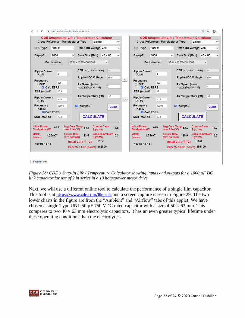
there are several packages available. For example, all three styles in Figure 1 are available. Let’s
choose a snap-in capacitor rated 105 °C such as our Type 381LX. The landing page linked in the
previous paragraph leads to our “double” (two side-by-side instances, facilitating what-if
scenario exploration) snap-in calculator at https://www.cde.com/Snapplet/DoubleSnapplet.htm
See the screen capture in Figure 28. We’ll be working with the left of the two applets, then later
using the arrow between them to automatically transfer a copy of this information over to the
right applet so we don’t have to type everything twice.
There is a Type drop-down box from which a 381LX is chosen, then the rated voltage,
capacitance, and case size are chosen, in that order; left to right, top to bottom is the best
workflow. The two ripple currents and frequencies are typed into the appropriate fields. The air
temperature near the capacitors we’ll assume is 55 °C and type that into the text box. Because
there will be two electrolytic capacitors in series, 350 V is entered as the applied voltage, as it is
half of the 700 VDC bus voltage in our earlier “rule of thumb” example.
Suppose the air temperature is known to be 55 °C but we wish to explore the effect of no forced
convection (i.e. natural convection only) compared to a little bit of airflow from a fan, such as 1
m/s air velocity. We leave the airspeed at 0 in the left applet, click the Calculate button, and
obtain an immediate estimate of 6.5 °C core rise and 162,800 hours lifetime. Now we can
transfer all that over to the right panel by clicking the “>>” arrow, then edit the airspeed in the
right panel, changing it from 0 to 1 m/s. After clicking Calculate in the right applet, we see that
the capacitor runs a little cooler and lasts a few years longer. Not only is the lifetime reported,
but also the ESR at the two frequencies at the predicted 60 °C core temperature is displayed as
19 mΩ at 300 Hz and 10 mΩ at 10 kHz. This underscores the strong effect that frequency often
has on the capacitor ESR.
Page 23 of 24 © 2020 Cornell Dubilier
Figure 28: CDE’s Snap-In Life / Temperature Calculator showing inputs and outputs for a 1000 µF DC
link capacitor for use of 2 in series in a 10 horsepower motor drive.
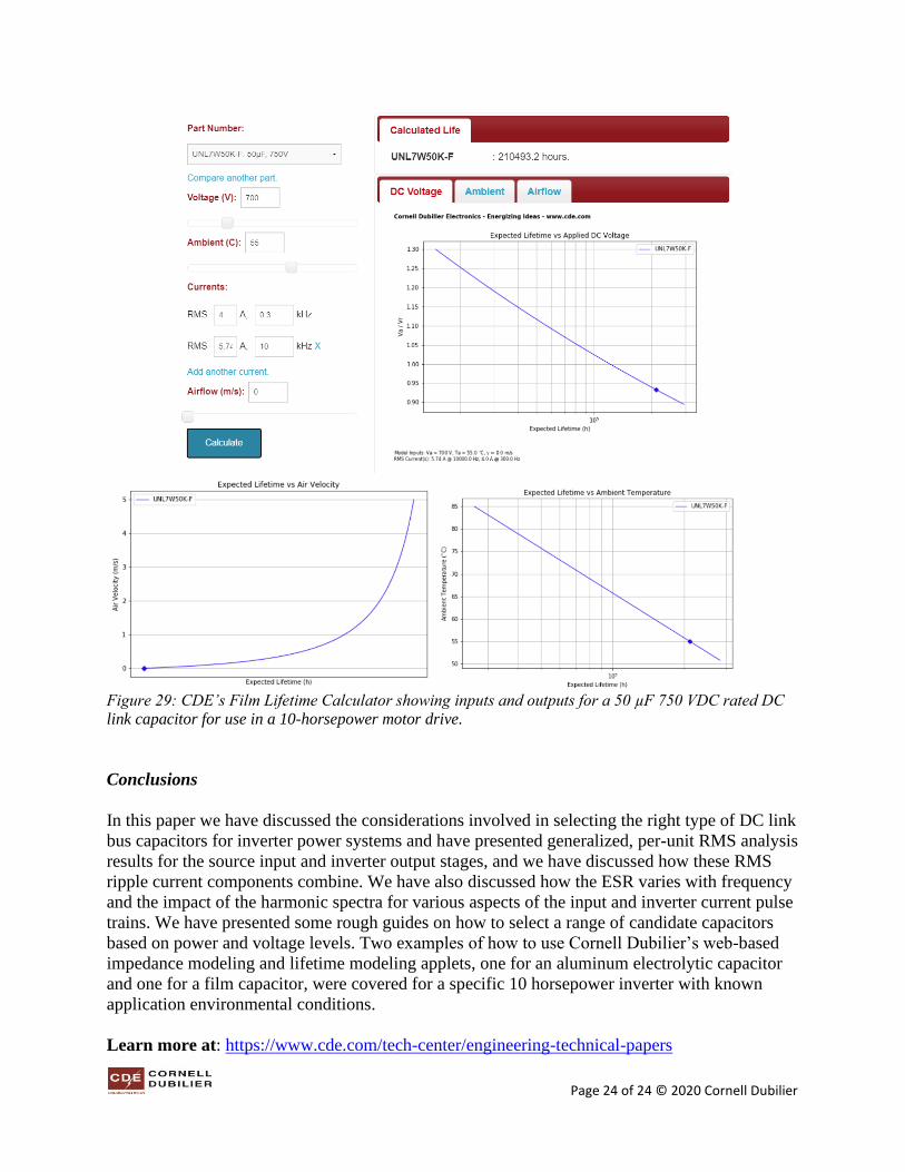
Next, we will use a different online tool to calculate the performance of a single film capacitor.
This tool is at https://www.cde.com/filmcalc and a screen capture is seen in Figure 29. The two
lower charts in the figure are from the “Ambient” and “Airflow” tabs of this applet. We have
chosen a single Type UNL 50 µF 750 VDC rated capacitor with a size of 50 × 63 mm. This
compares to two 40 × 63 mm electrolytic capacitors. It has an even greater typical lifetime under
these operating conditions than the electrolytics.
Page 24 of 24 © 2020 Cornell Dubilier
Figure 29: CDE’s Film Lifetime Calculator showing inputs and outputs for a 50 µF 750 VDC rated DC
link capacitor for use in a 10-horsepower motor drive.
Conclusions
In this paper we have discussed the considerations involved in selecting the right type of DC link
bus capacitors for inverter power systems and have presented generalized, per-unit RMS analysis
results for the source input and inverter output stages, and we have discussed how these RMS
ripple current components combine. We have also discussed how the ESR varies with frequency
and the impact of the harmonic spectra for various aspects of the input and inverter current pulse
trains. We have presented some rough guides on how to select a range of candidate capacitors
based on power and voltage levels. Two examples of how to use Cornell Dubilier’s web-based
impedance modeling and lifetime modeling applets, one for an aluminum electrolytic capacitor
and one for a film capacitor, were covered for a specific 10 horsepower inverter with known
application environmental conditions.
Learn more at: https://www.cde.com/tech-center/engineering-technical-papers