Embed Size (px)
Citation preview
Self-assembly of C60 monolayer on epitaxially grown, nanostructuredgraphene on Ru(0001) surfaceG. Li, H. T. Zhou, L. D. Pan, Y. Zhang, J. H. Mao et al. Citation: Appl. Phys. Lett. 100, 013304 (2012); doi: 10.1063/1.3673830 View online: http://dx.doi.org/10.1063/1.3673830 View Table of Contents: http://apl.aip.org/resource/1/APPLAB/v100/i1 Published by the American Institute of Physics. Related ArticlesSelf-assembly of C60 monolayer on epitaxially grown, nanostructured graphene on Ru(0001) surface APL: Org. Electron. Photonics 5, 4 (2012) High resolution patterning of nanoparticles by evaporative self-assembly enabled by in situ creation andmechanical lift-off of a polymer template Appl. Phys. Lett. 99, 253102 (2011) Morphology-dependent low-frequency Raman scattering in ultrathin spherical, cubic, and cuboid SnO2nanocrystals Appl. Phys. Lett. 99, 251902 (2011) Bismuth nano-droplets for group-V based molecular-beam droplet epitaxy Appl. Phys. Lett. 99, 243113 (2011) Fabrication of horizontal silicon nanowire arrays on insulator by ion irradiation AIP Advances 1, 042174 (2011) Additional information on Appl. Phys. Lett.Journal Homepage: http://apl.aip.org/ Journal Information: http://apl.aip.org/about/about_the_journal Top downloads: http://apl.aip.org/features/most_downloaded Information for Authors: http://apl.aip.org/authors
Downloaded 04 Jan 2012 to 159.226.37.1. Redistribution subject to AIP license or copyright; see http://apl.aip.org/about/rights_and_permissions
Self-assembly of C60 monolayer on epitaxially grown, nanostructuredgraphene on Ru(0001) surface
G. Li, H. T. Zhou, L. D. Pan, Y. Zhang, J. H. Mao, Q. Zou, H. M. Guo, Y. L. Wang, S. X. Du,and H.-J. Gaoa)
Institute of Physics, Chinese Academy of Sciences, Beijing, 100190, People’s Republic of China
(Received 14 September 2011; accepted 10 December 2011; published online 4 January 2012)
C60 molecules adsorbed on graphene/Ru(0001) substrate were investigated by scanning tunneling
microscopy (STM) at 5 K. On high quality substrates, C60 molecules adopt a commensurate growth
mode, leading to formation of a supramolecular structure with perfect periodicity and few defects.
On under-annealed substrates with imperfections and domains, the molecules form the same
closely packed hexagonal structures in spite of underlying corrugations, disorders or steps,
indicating a weak molecule-substrate interaction—a conclusion that is also supported by DFT
calculations. This system may be beneficial to the fabrication of carbon based devices and
of other types of organic functional overlayers. VC 2012 American Institute of Physics.
[doi:10.1063/1.3673830]
Since its discovery in 1985,1 C60 has attracted great in-
terest due not only to its unique structural and electronic
properties2,3 but also to its potential applications in various
fields.4–8 Extensive studies have been performed on the
adsorption and growth properties of C60 on different
substrates,2,3,9–14 including metal surfaces such as Cu(111),2
Ag(100),3 Ag(001),9 Au(111)10, and Ag(111)10 and semicon-
ductors like silicon11 and GaAs.12 On these flat surfaces, C60
molecules usually adopt a closely packed hexagonal growth
mode.2,9,10,12,13 Recently, more attentions have been paid on
the adsorption behaviors of C60 on patterned surface
structures.15–19 While many of these studies focused on trap-
ping C60 molecules by the superstructures, C60 monolayers
on periodically corrugated substrates were less investigated.
Based on regularly Moire structures, a kind of periodi-
cally corrugated template—graphene/Ru(0001) (G/Ru in the
following) has recently received lots of interest.20–25 Here,
we report a supramolecular structure of C60 molecules grown
on G/Ru surface. The periodic surface potential and the good
match between the template and the lattice of adsorbed mol-
ecules are the dominant factors for this supramolecular struc-
ture. By carefully analyzing C60 growth on under-annealed
graphene, we found that the interaction between the C60 mo-
lecular layer and the substrate was rather weak. Density
functional theory (DFT) study of adsorption energy and the
observation of tip-induced rotation of C60 molecules both
also support our result. This weak molecule-substrate inter-
action should be responsible for the continuous and uniform
nature of the molecular layer.
The experiments were conducted in an Omicron low
temperature STM system under a base pressure better than
1.0� 10�10 mbar. The G/Ru template was fabricated follow-
ing the same technique as described in a previous study21
except that some of the samples were intentionally under-
annealed (�1100 K) to create imperfections and domains.
C60 (99.5% purity, Aldrich) molecules were evaporated at
600 K onto the samples (kept at room temperature) followed
by annealing at 320 K for 1 h. Then, these samples were
transferred to low temperature chamber (�5 K) for scanning.
Our theoretical calculations were based on DFT by Vienna
ab-initio simulation package (VASP).26 Projector augmented
wave (PAW) potentials27 and local density approximation
(LDA)28 for exchange correlation potential were used. The
periodic models included a fixed rippling 12� 12 graphene
super lattice with a C60 molecule adsorbing on three different
surface sites (fcc, hcp, atop)21 and a vacuum layer of 12 A.
The C60 molecules were fully relaxed until the net force on
every atom was less than 0.01 eV/A. In our calculation, the
energy cutoff of the plane-wave basis sets was 400 eV, and a
single C point was employed for Brillouin zone matrix inte-
grations due to the numerical limitations.
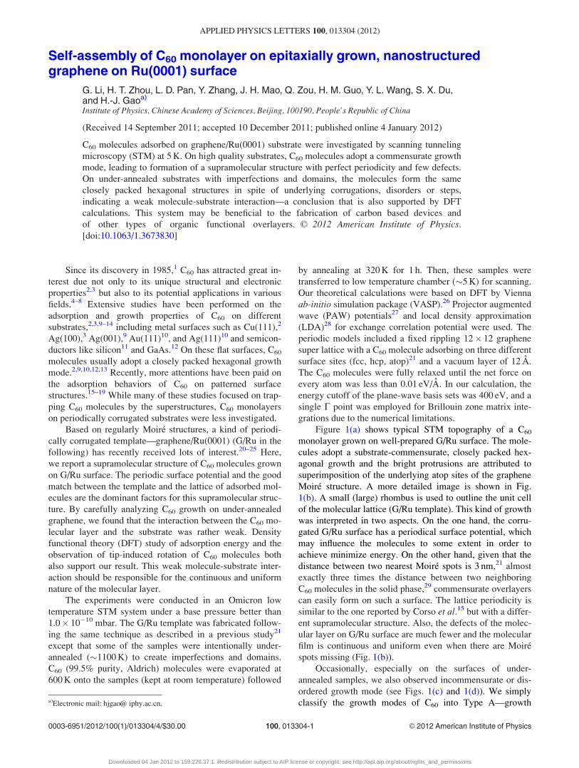
Figure 1(a) shows typical STM topography of a C60
monolayer grown on well-prepared G/Ru surface. The mole-
cules adopt a substrate-commensurate, closely packed hex-
agonal growth and the bright protrusions are attributed to
superimposition of the underlying atop sites of the graphene
Moire structure. A more detailed image is shown in Fig.
1(b). A small (large) rhombus is used to outline the unit cell
of the molecular lattice (G/Ru template). This kind of growth
was interpreted in two aspects. On the one hand, the corru-
gated G/Ru surface has a periodical surface potential, which
may influence the molecules to some extent in order to
achieve minimize energy. On the other hand, given that the
distance between two nearest Moire spots is 3 nm,21 almost
exactly three times the distance between two neighboring
C60 molecules in the solid phase,29 commensurate overlayers
can easily form on such a surface. The lattice periodicity is
similar to the one reported by Corso et al.15 but with a differ-
ent supramolecular structure. Also, the defects of the molec-
ular layer on G/Ru surface are much fewer and the molecular
film is continuous and uniform even when there are Moire
spots missing (Fig. 1(b)).
Occasionally, especially on the surfaces of under-
annealed samples, we also observed incommensurate or dis-
ordered growth mode (see Figs. 1(c) and 1(d)). We simply
classify the growth modes of C60 into Type A—growtha)Electronic mail: hjgao@ iphy.ac.cn.
0003-6951/2012/100(1)/013304/4/$30.00 VC 2012 American Institute of Physics100, 013304-1
APPLIED PHYSICS LETTERS 100, 013304 (2012)
Downloaded 04 Jan 2012 to 159.226.37.1. Redistribution subject to AIP license or copyright; see http://apl.aip.org/about/rights_and_permissions
commensurate with the substrate and Type B—growth that
seems disordered. Type B areas occur less frequently and are
most likely to appear upon or adjacent to imperfections and
domain boundaries, which we suppose to cause their forma-
tion. Domain-related Type B growth is incommensurate with
the substrate and usually happens when a C60 island is
stretched across two or more domains (see, e.g., the upper
part of Fig. 1(c)). Hence, this kind of area is sometimes very
large in size when C60 coverage reached 1 monolayer. In
Fig. 1(d)), a typical domain-related Type B area is displayed.
Since the positions of graphene Moire spots cannot be
clearly resolved in this case, we applied the Fourier trans-
form (FT) to the initial image, as shown in the inset. The
outer six points correspond to the C60 molecular lattice and
the inner ones represent the Moire pattern’s periodicity. By
measuring the angle between vectors q1 and q2 in the FT
image, we found that the two periodic lattices are rotated by
26� with respect to each other. However, this is not the only
rotation value we obtained. Among the samples we investi-
gated, such angles range from 4� to 26�, indicating a random
relationship between the orientations of the two lattices. This
further supports our supposition that incommensurate growth
has something to do with domain boundaries, since Moire
pattern domains also have random directions in our samples.
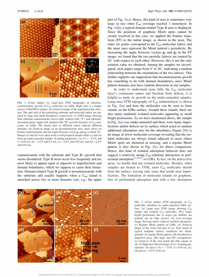
In order to understand more fully the C60 molecular
layer’s continuous nature and freedom from defects, it is
helpful to study its growth on the under-annealed samples.
Large-area STM topography of C60 submonolayer is shown
in Fig. 2(a) and here the molecules can be seen to form
islands on the G/Ru surface. Around these islands, there are
also many randomly isolated molecules appearing as small
bright protrusions. As we have mentioned above, the sample
in Fig. 2(a) was under-annealed and there were many imper-
fections and/or defects on its surface which acted as random
additional adsorption sites for the adsorbates. Figure 2(b) is
an image at lower molecular coverage revealing that the iso-
lated molecules are always found adjacent to areas where
Moire spots are distorted or missing, and a regular Moire
pattern is also shown in Fig. 2(c) for direct comparison.
Hence, this kind of isolated adsorption behavior does not
suggest a relatively strong C60-substrate interaction or pref-
erential adsorption11,22,23 on G/Ru. In fact, on the defect-free
areas, we hardly find any isolated molecules. Besides, when
samples are heated to 370 K, most C60 molecules desorb
from the surface, leaving only some that reside near imper-
fections. The formation of molecular islands on graphene,
free of preferential adsorption and with a low desorption
FIG. 1. (Color online) (a) Large-area STM topography of substrate-
commensurate growth of C60 molecules on G/Ru. Right part is a higher
terrace of Ru(0001) surface. (b) Zoom-in image of the supramolecular struc-
ture. The unit cells of the underlying substrate and molecular lattice are out-
lined by large and small rhombuses, respectively. (c) STM image showing
both substrate-commensurate (lower right, marked with “A”) and substrate-
incommensurate (upper left, marked with “B”) growth structure of C60 mol-
ecules on G/Ru. The dotted lines in different colors indicate different
domains. (d) Zoom-in image of an incommensurate area. Inset shows its
Fourier transformation and the angle between vector q1 and q2 is about 26�.Images (a) and (b) were taken from a well prepared sample while (c) and (d)
from an under-annealed sample. Scanning parameters: (a) Vs¼�3.0 V and
I¼ 0.05 nA, (b) �2.0 V and 0.1 nA, (c) þ2.0 V and 0.05 nA, and (d) þ2.0 V
and 0.03 nA.
FIG. 2. (Color online) STM topography of C60
molecules adsorbed on under-annealed G/Ru sur-
face: (a) Large area STM image showing C60
islands and isolated C60 molecules. Five larger
bright protrusions due to argon gas bubbles are
pointed out by blue arrows. (b) Low-coverage
image showing defect induced isolated adsorption.
(c) Regular Moire pattern of G/Ru. (d) Zoom-in
image of the lower left part of (a). Four kinds of
typical template surface conditions are distin-
guished: (I) regular Moire pattern, (II) disordered or
imperfect areas, (III) steps, and (IV) corrugations.
(e) Zoom-in of the area inside the blue square in
(d). (f) High-pass filtered image of (e). Scanning pa-
rameters: (b) and (c) Vs¼�3.0 V, I¼ 0.05 nA, (a),
(d) and (e) þ3.0 V, 0.02 nA.
013304-2 Li et al. Appl. Phys. Lett. 100, 013304 (2012)
Downloaded 04 Jan 2012 to 159.226.37.1. Redistribution subject to AIP license or copyright; see http://apl.aip.org/about/rights_and_permissions
temperature indicate that interactions between adsorbed mol-
ecules and the substrate are rather weak. We can also see
that Ru substrate has minor influences on C60 molecules
compared with some previously studied molecules and
atoms22,23,25 since C60 does not show any difference on the
adsorption on three different surface sites.
In Fig. 2(a), the larger bright protrusions pointed out by
blue arrows are attributed to argon gas bubbles lying a few
atomic layers beneath the Ru(0001) surface.30 Thus, the sur-
face in Fig. 2(a) contains four different types of areas: a reg-
ular Moire pattern, imperfections, steps, and argon gas
related protrusions. These are labeled in Fig. 2(d) as I, II, III,
and IV, respectively. C60 molecular island extends over all
the four types of surface areas smoothly. To investigate the
arrangement of the C60 molecules, we further zoom in part
of the island (Fig. 2(e)) and find that they also adopt a closely
packed hexagonal growth mode. After high-pass filtering,
the molecular lattice was made visible in Fig. 2(f). Surpris-
ingly, the lattice is rather well ordered, indicating that
the hexagonal packing behavior is retained regardless of
underlying imperfections, protrusions, or steps. We empha-
size that the height of the steps and protrusions ranges from
0.2� 0.3 nm, and the uniform molecular lattice suggests a
strong C60-C60 interaction compared with the C60-substrate
interaction.
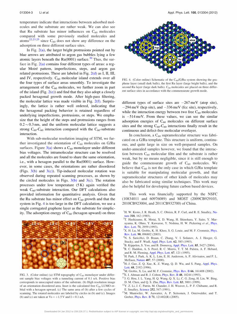
With sub-molecular resolution imaging of STM, we fur-
ther investigated the orientation of C60 molecules on G/Ru
surfaces. Figure 3(a) shows a C60 monolayer under different
bias voltages. The intramolecular structure can be resolved
and all the molecules are found to share the same orientation,
i.e., with a hexagon parallel to the Ru(0001) surface. How-
ever, in some cases, the orientations are rather disordered
(Figs. 3(b) and 3(c)). Tip-induced molecular rotation was
observed during repeated scanning processes, as shown by
the circled molecules in Figs. 3(b) and 3(c). The rotation
processes under low temperature (5 K) again verified the
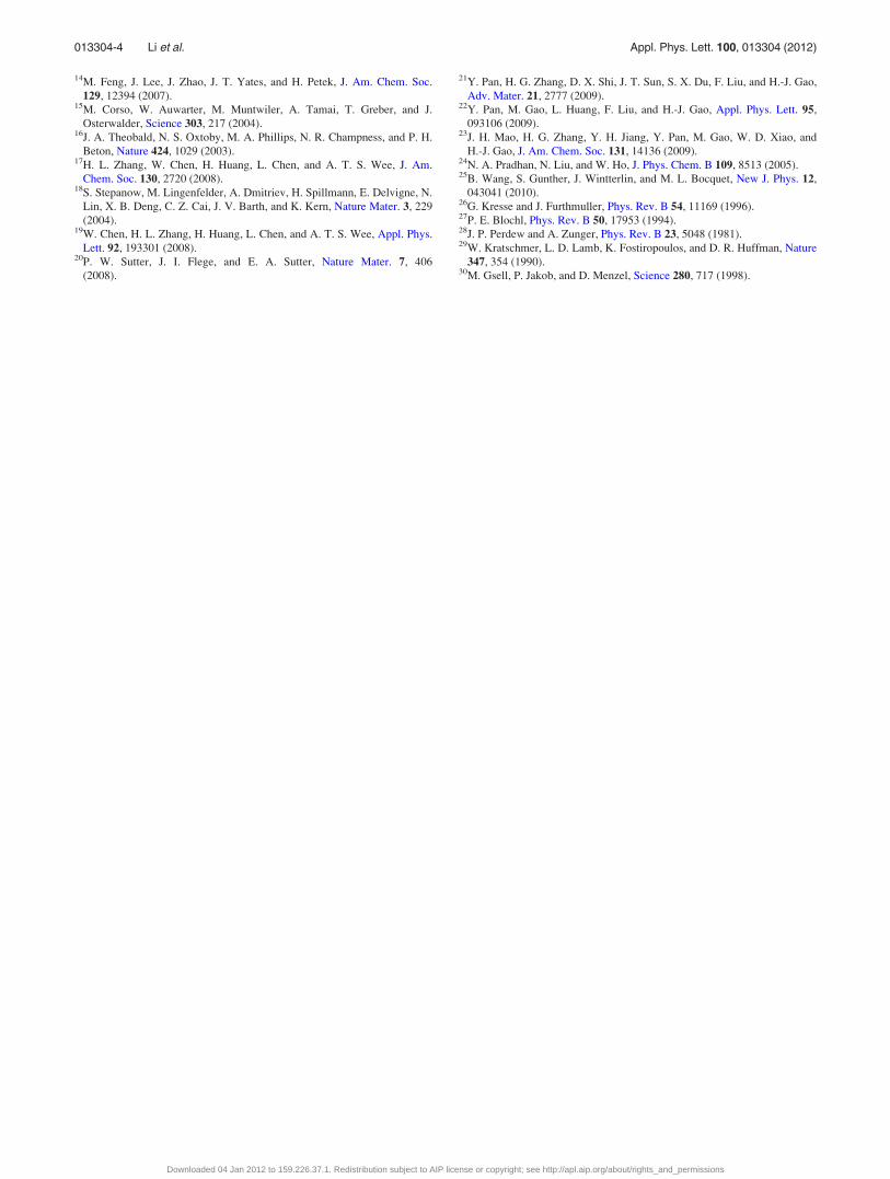
weak C60-substrate interaction. Our DFT calculations also
provided information for quantitative analysis. Given that
the Ru substrate has minor effect on C60 growth and that the
system in Fig. 4 is too large in the DFT calculation, we use a
single corrugated graphene layer as the substrate for simplic-
ity. The adsorption energy of C60 (hexagon upward) on three
different types of surface sites are �267 meV (atop site),
�294 meV (hcp site), and �336 meV (fcc site), respectively,
while the interaction energy between two free C60 molecules
is �514 meV. From these values, we can see the similar
adsorption energies of C60 molecules on different surface
sites and the strong C60-C60 interactions finally result in the
continuous and defect-free molecular overlayer.
In conclusion, a C60 supramolecular structure was fabri-
cated on a G/Ru template. This structure is uniform, continu-
ous, and quite large in size on well-prepared samples. On
under-annealed samples however, we found that the interac-
tion between C60 molecular film and the substrate is rather
weak, but by no means negligible, since it is still enough to
guide the commensurate growth of C60 molecules. We
believe that C60 is not the only case in which G/Ru template
is suitable for manipulating molecular growth, and that
supramolecular structures of other kinds of molecules may
also be fabricated using similar techniques. This work may
also be helpful for developing future carbon based devices.
This work was financially supported by the NSFC
(10834011 and 60976089) and MOST (2009CB929103,
2010CB923004, and 2011CB932700) of China.
1H. W. Kroto, J. R. Heath, S. C. Obrien, R. F. Curl, and R. E. Smalley, Na-
ture 318, 162 (1985).2T. Hashizume, K. Motai, X. D. Wang, H. Shinohara, Y. Saito, Y. Mar-
uyama, K. Ohno, Y. Kawazoe, Y. Nishina, H. W. Pickering et al., Phys.
Rev. Lett. 71, 2959 (1993).3X. H. Lu, M. Grobis, K. H. Khoo, S. G. Louie, and M. F. Crommie, Phys.
Rev. Lett. 90, 096802 (2003).4N. S. Sariciftci, D. Braun, C. Zhang, V. I. Srdanov, A. J. Heeger, G.
Stucky, and F. Wudl, Appl. Phys. Lett. 62, 585 (1993).5B. Kippelen, S. Yoo, and B. Domercq, Appl. Phys. Lett. 85, 5427 (2004).6R. C. Haddon, A. S. Perel, R. C. Morris, T. T. M. Palstra, A. F. Hebard,
and R. M. Fleming, Appl. Phys. Lett. 67, 121 (1995).7H. Park, J. Park, A. K. L. Lim, E. H. Anderson, A. P. Alivisatos, and P. L.
McEuen, Nature 407, 57 (2000).8H.-J. Gao, Z. Q. Xue, K. Z. Wang, Q. D. Wu, and S. Pang, Appl. Phys.
Lett. 68, 2192 (1996).9M. Grobis, X. Lu, and M. F. Crommie, Phys. Rev. B 66, 161408 (2002).
10E. I. Altman and R. J. Colton, Phys. Rev. B 48, 18244 (1993).11J. G. Hou, J. L. Yang, H. Q. Wang, Q. X. Li, C. G. Zeng, H. Lin, W. Bing,
D. M. Chen, and Q. S. Zhu, Phys. Rev. Lett. 83, 3001 (1999).12Y. Z. Li, J. C. Patrin, M. Chander, J. H. Weaver, L. P. F. Chibante, and R.
E. Smalley, Science 252, 547 (1991).13M. Muntwiler, W. Auwarter, A. P. Seitsonen, J. Osterwalder, and T.
Greber, Phys. Rev. B 71, 121402(R) (2005).
FIG. 3. (Color online) (a) STM topography of C60 monolayer under differ-
ent sample bias voltages with a tunneling current of 0.1 nA. Positive bias
corresponds to unoccupied states of the substrate. (b) High resolution image
of an orientation disordered area. Inset is the calculated free C60 LUMO or-
bital with a hexagon upward. (c) The same area of (b) after a few cycles of
scanning. The rotated molecules are labeled by circles in (b) and (c). Images
(b) and (c) are taken at Vs¼þ1.5 V and I¼ 0.1 nA.
FIG. 4. (Color online) Schematic of the C60/G/Ru system showing the gra-
phene layer (small dark balls), the first Ru layer (large bright balls), and the
second Ru layer (large dark balls). C60 molecules are placed on three differ-
ent surface sites in accordance with the commensurate growth mode.
013304-3 Li et al. Appl. Phys. Lett. 100, 013304 (2012)
Downloaded 04 Jan 2012 to 159.226.37.1. Redistribution subject to AIP license or copyright; see http://apl.aip.org/about/rights_and_permissions
14M. Feng, J. Lee, J. Zhao, J. T. Yates, and H. Petek, J. Am. Chem. Soc.
129, 12394 (2007).15M. Corso, W. Auwarter, M. Muntwiler, A. Tamai, T. Greber, and J.
Osterwalder, Science 303, 217 (2004).16J. A. Theobald, N. S. Oxtoby, M. A. Phillips, N. R. Champness, and P. H.
Beton, Nature 424, 1029 (2003).17H. L. Zhang, W. Chen, H. Huang, L. Chen, and A. T. S. Wee, J. Am.
Chem. Soc. 130, 2720 (2008).18S. Stepanow, M. Lingenfelder, A. Dmitriev, H. Spillmann, E. Delvigne, N.
Lin, X. B. Deng, C. Z. Cai, J. V. Barth, and K. Kern, Nature Mater. 3, 229
(2004).19W. Chen, H. L. Zhang, H. Huang, L. Chen, and A. T. S. Wee, Appl. Phys.
Lett. 92, 193301 (2008).20P. W. Sutter, J. I. Flege, and E. A. Sutter, Nature Mater. 7, 406
(2008).
21Y. Pan, H. G. Zhang, D. X. Shi, J. T. Sun, S. X. Du, F. Liu, and H.-J. Gao,
Adv. Mater. 21, 2777 (2009).22Y. Pan, M. Gao, L. Huang, F. Liu, and H.-J. Gao, Appl. Phys. Lett. 95,
093106 (2009).23J. H. Mao, H. G. Zhang, Y. H. Jiang, Y. Pan, M. Gao, W. D. Xiao, and
H.-J. Gao, J. Am. Chem. Soc. 131, 14136 (2009).24N. A. Pradhan, N. Liu, and W. Ho, J. Phys. Chem. B 109, 8513 (2005).25B. Wang, S. Gunther, J. Wintterlin, and M. L. Bocquet, New J. Phys. 12,
043041 (2010).26G. Kresse and J. Furthmuller, Phys. Rev. B 54, 11169 (1996).27P. E. Blochl, Phys. Rev. B 50, 17953 (1994).28J. P. Perdew and A. Zunger, Phys. Rev. B 23, 5048 (1981).29W. Kratschmer, L. D. Lamb, K. Fostiropoulos, and D. R. Huffman, Nature
347, 354 (1990).30M. Gsell, P. Jakob, and D. Menzel, Science 280, 717 (1998).
013304-4 Li et al. Appl. Phys. Lett. 100, 013304 (2012)
Downloaded 04 Jan 2012 to 159.226.37.1. Redistribution subject to AIP license or copyright; see http://apl.aip.org/about/rights_and_permissions