Embed Size (px)
Citation preview

Semiconductor Devices, Fall 2014
Gunnar Malm, Associate Professor Integrated Devices and Circuits, Kista Campus [email protected], 08-790 4332
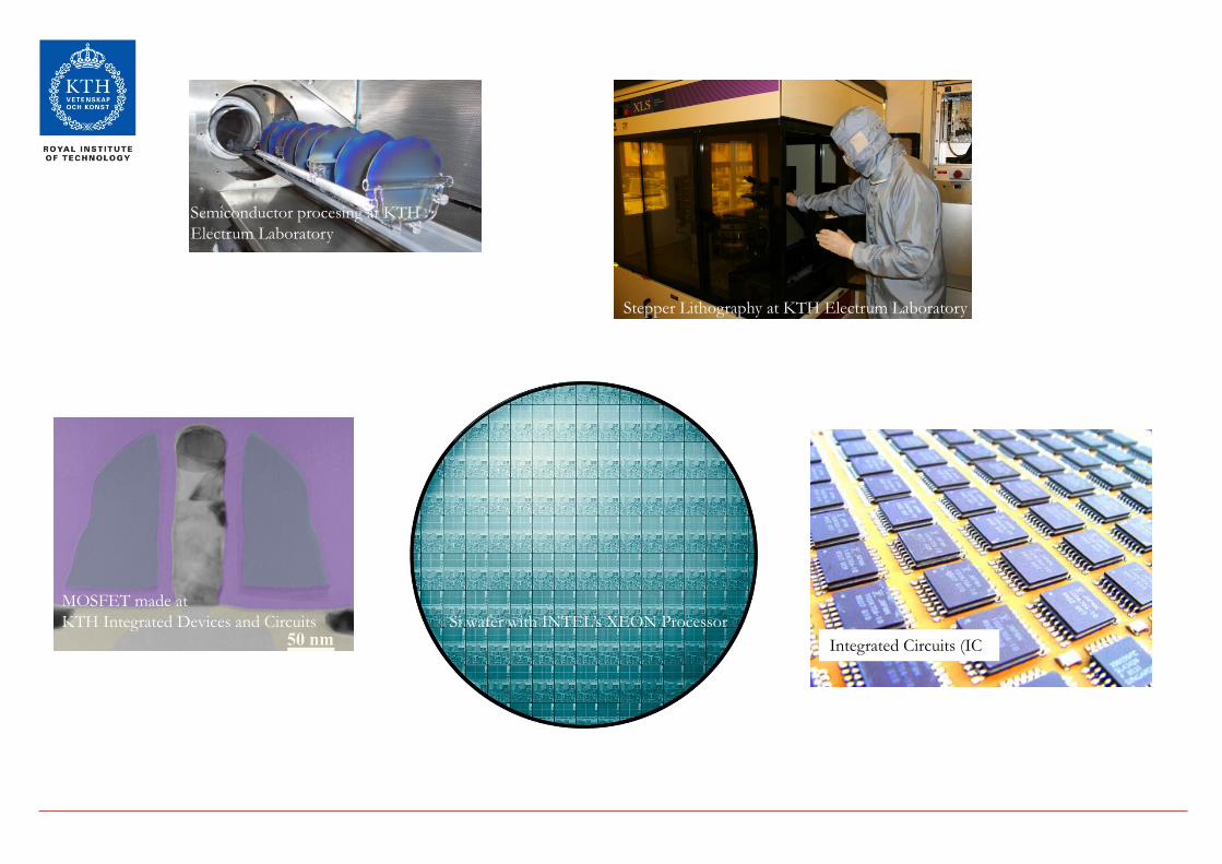
Semiconductor procesing at KTH Electrum Laboratory
Stepper Lithography at KTH Electrum Laboratory
Si wafer with INTEL’s XEON Processor MOSFET made at KTH Integrated Devices and Circuits
Integrated Circuits (IC)
Today’s lecture & introduction
•Course info (approx first hour) •Semiconductor material properties and history •Concepts
- Conduction electrons in a SC crystal
Course goals The overall goal of the course is that you should be able to describe the function of the pn-diode, the bipolar and the MOS transistor and how these three devices are used in applications. You should be able to derive and calculate the currents inside these devices and be able to analyse the internal state of the charge distribution, the electric field and the current density.
In detail, after a successful completion of the course you will be able to:
1. qualitatively describe the electronic energy band structure of insulators, semiconductors and metals 2. calculate the electron and hole concentration in the conduction and valence band using Fermi-Dirac
statistics and the energy band model. 3. describe the constituents of the current density in semiconductors and derive analytical expressions for
the current density in the case of low-level injection, electron-hole recombination, externally applied voltage and external generation by light, using the drift-diffusion model.
4. describe the function of the pn-diode, the bipolar and the long channel MOS transistor. 5. analyse and calculate the internal electrostatics (electric charge, electric field and potential) of the pn-
diode, the bipolar and the long channel MOS transistor. 6. derive and calculate the current density in the pn-diode, the bipolar and the long channel MOS transistor
using the drift-diffusion model. 7. describe major process technologies, used to fabricate semiconductor devices and relate these to
schematic cross-section drawings of devices. 8. extract device properties from electrical measurements of devices. 9. perform oral and written presentation of the subject Semiconductor Components.
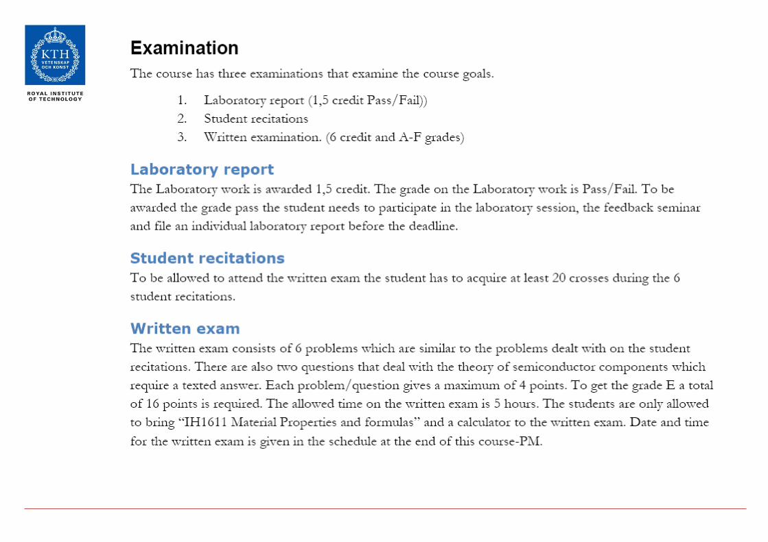
Student recitations There are 6 student recitations in the course. At the first lectures 6 sheets containing 6 problems (totally 36 problems) are distributed. The sheets are numbered as S1, S2, S3, S4, S5 and S6. Before each student recitations the student should try to solve the 6 problems on the sheet related to the student recitation in question. The student should also prepare to present the solution on the board for the class.
The level of difficulty of the problems on the student recitation corresponds to the written exam.
In detail a student recitation is organized as follows:
1. At the beginning of the student recitation each student will put a cross on a list to indicate which of the 6 problems he/she is prepared to present to the class
2. One student is randomly picked to present each problem. 3. After the solution has been presented there is a discussion, in which all students
are expected to participate. Students are expected to give feedback on the presented solution and possibly provide alternative solutions.
4. When the discussion is finished a new student presents a solution to the next problem
5. When all 6 problems have been presented and discussed the student recitation ends.
The number of crosses a student has on the list indicates how many problem the student has solved. The total number of problems is 36. To be allowed to attend the written exam the student has to acquire a minimum of 20 crosses after the 6 student recitations.
Laboratory work, seminars and report Course lab includes a laboratory exercise in groups of four students. The place of the lab is in the Electrum building, elevator C, level 4. Labs will be scheduled by signup in the Daisy portal. During two hours measurement data are collected under the guidance of a lab assistant. After the lab, each student independently determines device parameters from measurements. Each student receives an individual assignment and will write an individual lab report that presents the measurements, the extraction procedure and the results. Method, results and conclusions must be clearly outlined. Results should be commented on regarding accuracy and students are expected to reflect on the relationship between measurements and theory. Results should be reported with well-structured diagrams, graphs and tables. A good lab report should be clear, as well as linguistically well-written. The first seminar deals with extraction procedure and with report writing .
The laboratory report should be sent by email to the course responsible in PDF before the first deadline stated in the schedule at the end of this course-PM.
The laboratory report will be tested for plagiarism of the course responsible. All students will receive an email with three laboratory reports. These should be read and about half a page constructive feedback must be prepared before the feedback seminar. The written feedback should be brought in two copies (one to their peers and one to the course responsible) to the feedback seminar (date and time is given in the schedule at the end of this course-PM). At the feedback seminar each student will give (to their peers) and receive (from their peers) feedback on their reports. After the seminar students can improve their reports and the final report should be sent in to the course responsible before the second deadline stated in the schedule at the end of this course-PM.
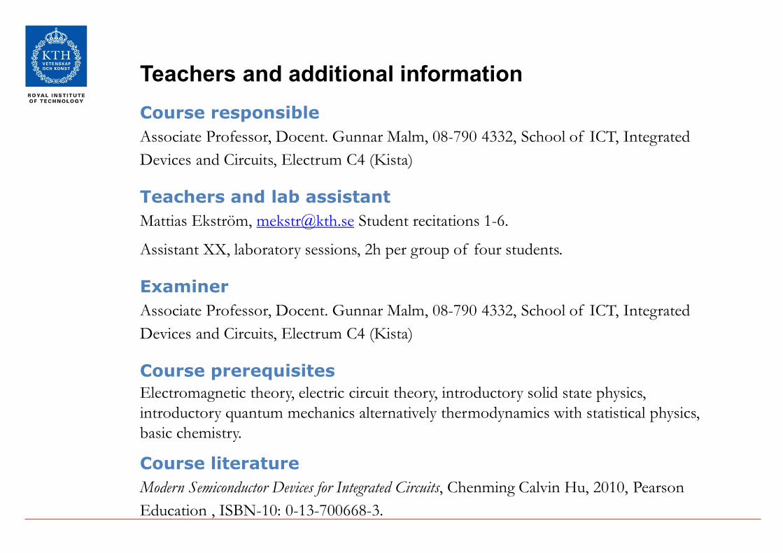
Teachers and additional information Course responsible Associate Professor, Docent. Gunnar Malm, 08-790 4332, School of ICT, Integrated Devices and Circuits, Electrum C4 (Kista)
Teachers and lab assistant Mattias Ekström, [email protected] Student recitations 1-6.
Assistant XX, laboratory sessions, 2h per group of four students.
Examiner Associate Professor, Docent. Gunnar Malm, 08-790 4332, School of ICT, Integrated Devices and Circuits, Electrum C4 (Kista)
Course prerequisites Electromagnetic theory, electric circuit theory, introductory solid state physics, introductory quantum mechanics alternatively thermodynamics with statistical physics, basic chemistry.
Course literature Modern Semiconductor Devices for Integrated Circuits, Chenming Calvin Hu, 2010, Pearson Education , ISBN-10: 0-13-700668-3.
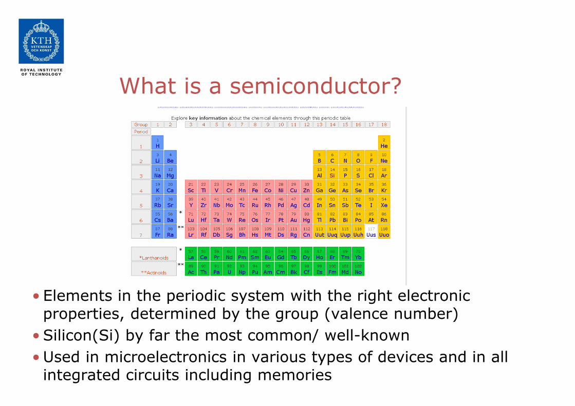
What is a semiconductor?
• Elements in the periodic system with the right electronic properties, determined by the group (valence number) •Silicon(Si) by far the most common/ well-known •Used in microelectronics in various types of devices and in all
integrated circuits including memories
•Which of the following statements are correct?
A) The semiconductors were discovered before electronics
B) Analog electronics can be realized without semiconductors
C) Digital electronics can be realized without semiconductors
D) Radio development pushed the semiconductor technology
Are you sure about your answer? - I am guessing
- I am quite sure - I am correct
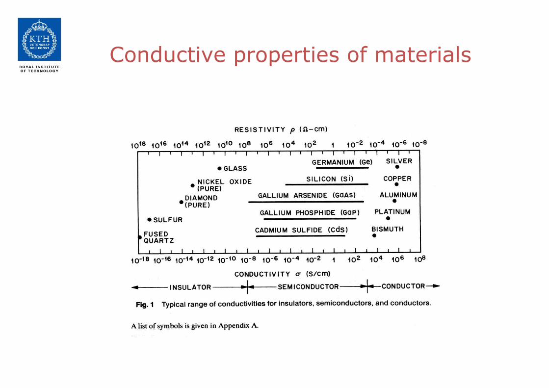
Conductive properties of materials
•Which of the following statements are correct? For a semiconductor you can easily change the conductivity by the following means:
A) Changing the temperatures
B) Changing the lightning ambient C) Adding impurities to the material D) Changing the pressure (acting on the sample)
Are you sure about your answer? - I am guessing
- I am quite sure - I am correct
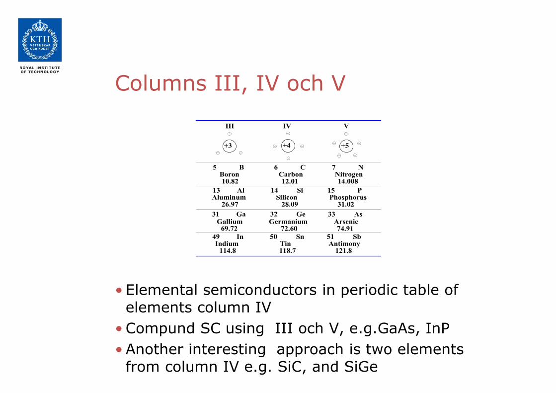
Columns III, IV och V
+5+3 +4
10.82 12.01 14.008 Boron Carbon Nitrogen5 B 6 C 7 N
III IV V
26.97 28.09 31.02 Aluminum Silicon Phosphorus13 Al 14 Si 15 P
69.72 72.60 74.91 Gallium Germanium Arsenic31 Ga 32 Ge 33 As
114.8 118.7 121.8 Indium Tin Antimony49 In 50 Sn 51 Sb
• Elemental semiconductors in periodic table of elements column IV •Compund SC using III och V, e.g.GaAs, InP •Another interesting approach is two elements
from column IV e.g. SiC, and SiGe
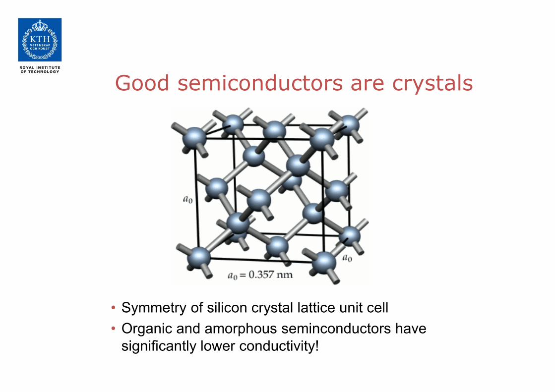
Good semiconductors are crystals
• Symmetry of silicon crystal lattice unit cell • Organic and amorphous seminconductors have
significantly lower conductivity!
•Silicon has co-valent bonding • Each atom has four nearest neighbours •GaAs has the same crystal structure with 50 % Ga and 50 % As
Si
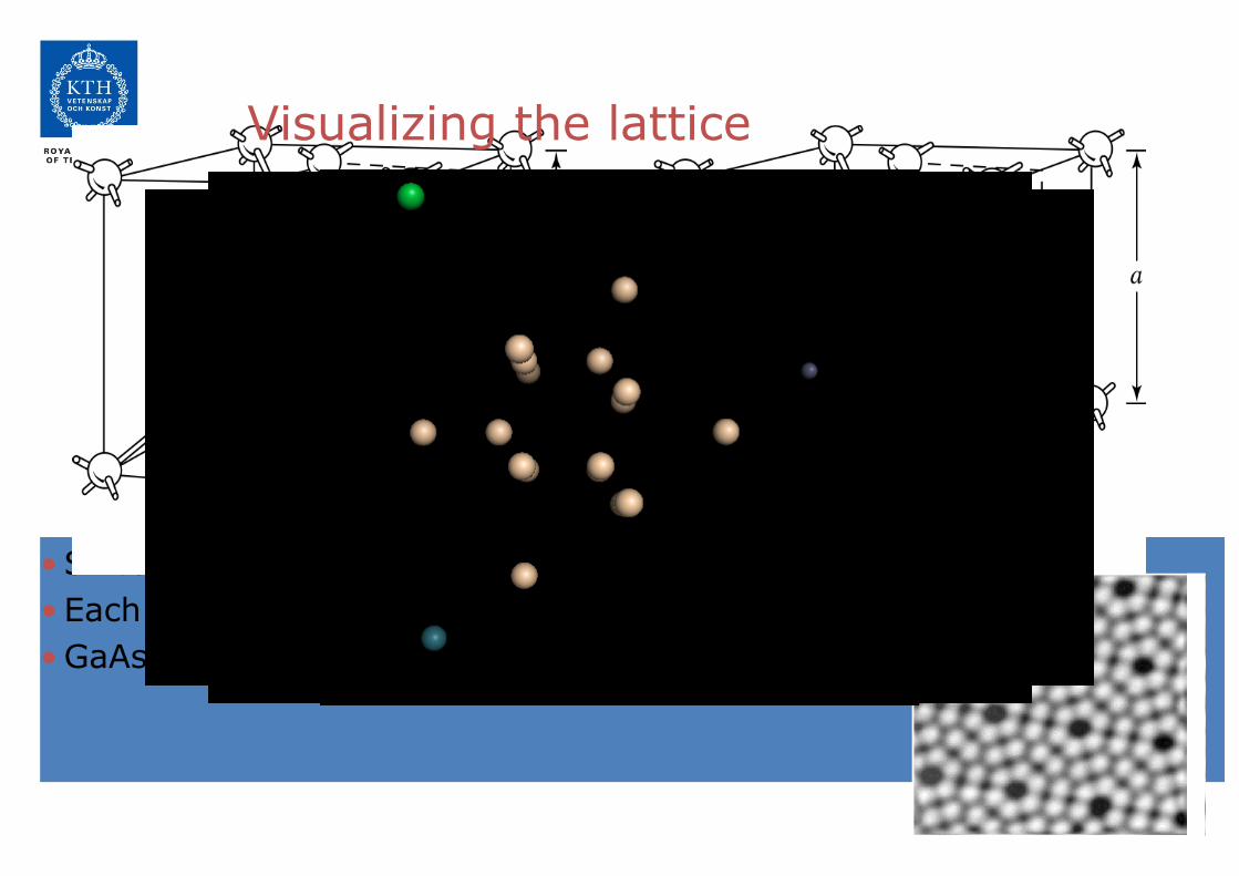
Visualizing the lattice
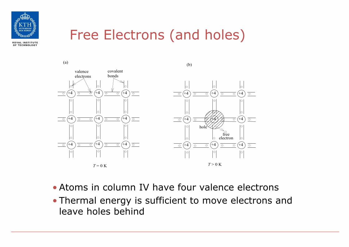
T = 0 K
(a)
+4 +4
+4
+4+4 +4
+4+4
bonds
+4
valenceelectrons
covalent
+4 +4
+4
+4+4 +4
+4+4
free
+4
electron
hole
(b)
T > 0 K
Free Electrons (and holes)
•Atoms in column IV have four valence electrons • Thermal energy is sufficient to move electrons and
leave holes behind
+4 +4
+4+4 +4
+4
+4+4
+4 +4
+4+4 +4
+4
+4+4
electron
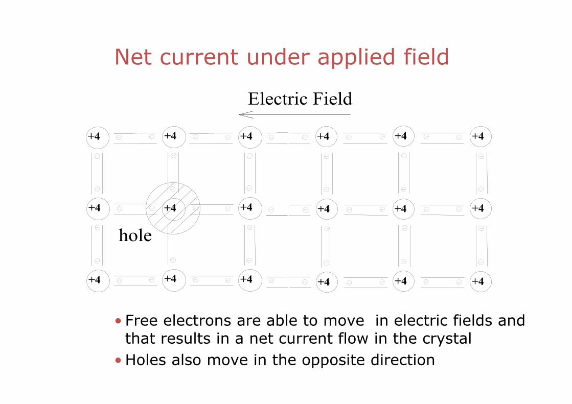
Electric Field
+4
hole+4
freeelectron
+4 +4
+4+4 +4
+4
+4+4
+4 +4
+4+4 +4
+4
+4+4
electron
Electric Field
+4
hole+4
+4 +4
+4+4 +4
+4
+4+4
+4 +4
+4+4 +4
+4
+4+4
electron
Electric Field
+4
hole+4
Net current under applied field
• Free electrons are able to move in electric fields and that results in a net current flow in the crystal •Holes also move in the opposite direction
Next Lecture
•Reading 1.1-9 and 1.11, 2.1-2.2 •Concepts:
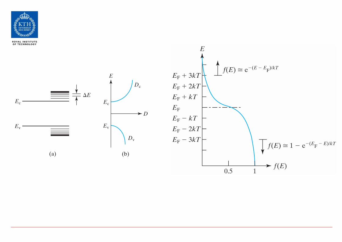
- Energy band model - Distribution functions and effective density of states - Intrinsic carriers and ionized dopant impurities - Charge neutrality - Drift current (applied field)


![Semiconductor Devices [Kanaan Kano]](https://img.pdfslide.net/doc/110x75/55cf931a550346f57b9bb747/semiconductor-devices-kanaan-kano.jpg)