Embed Size (px)
Citation preview
Semiconductor Devices Fall 2014
Gunnar Malm, Associate Professor Integrated Devices and Circuits, Kista Campus [email protected], 08-790 4332
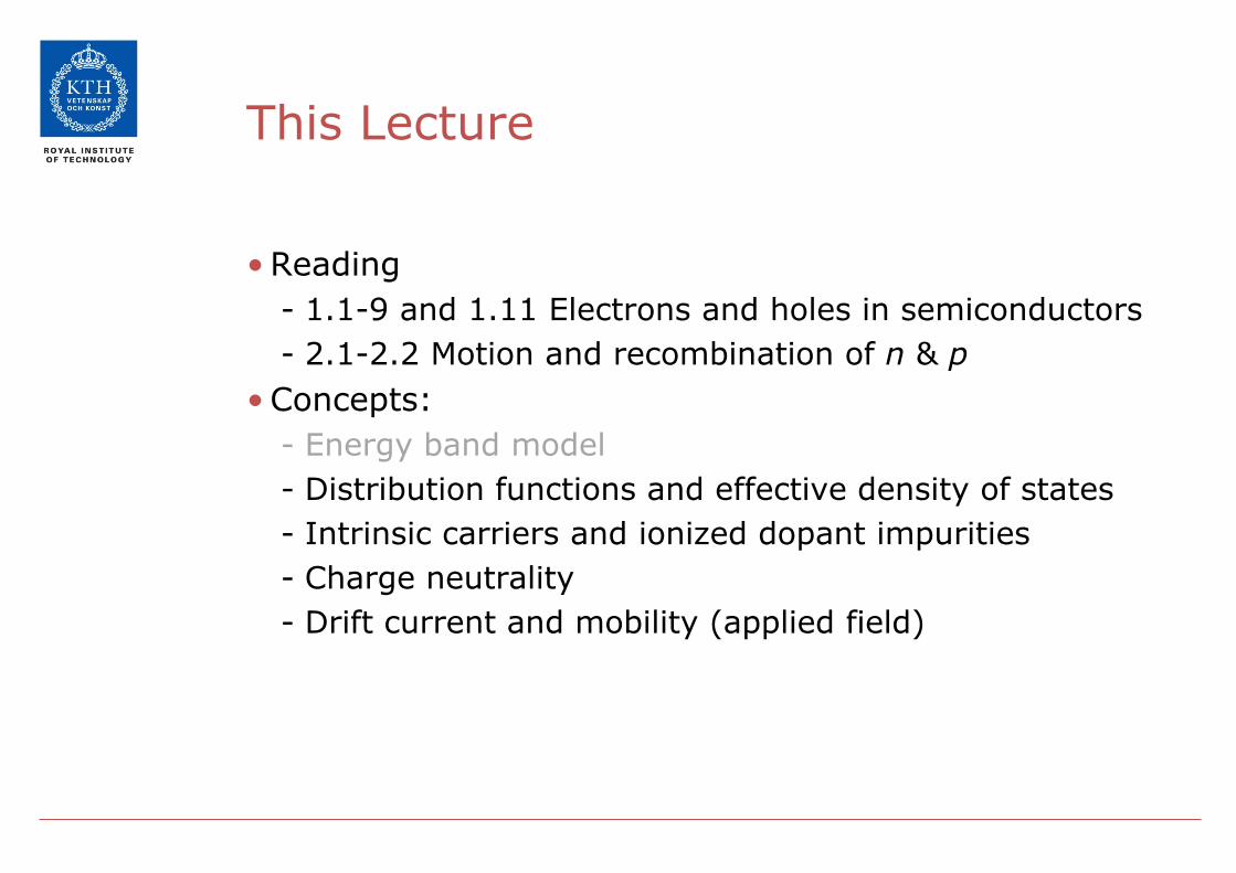
This Lecture
•Reading - 1.1-9 and 1.11 Electrons and holes in semiconductors - 2.1-2.2 Motion and recombination of n & p
•Concepts: - Energy band model - Distribution functions and effective density of states - Intrinsic carriers and ionized dopant impurities - Charge neutrality - Drift current and mobility (applied field)
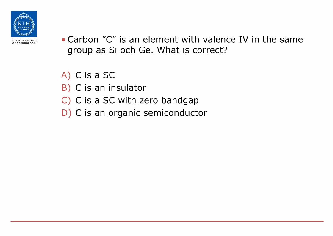
•Carbon ”C” is an element with valence IV in the same group as Si och Ge. What is correct?
A) C is a SC B) C is an insulator C) C is a SC with zero bandgap D) C is an organic semiconductor
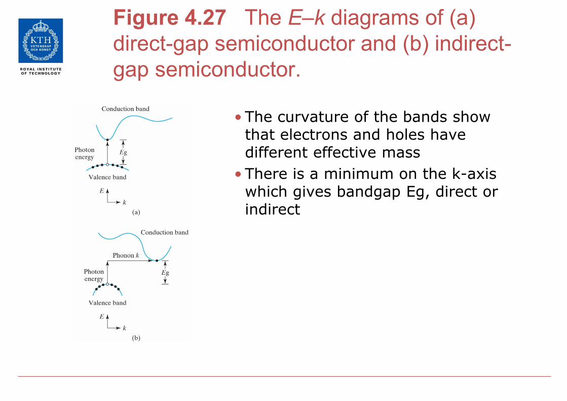
Figure 4.27 The E–k diagrams of (a) direct-gap semiconductor and (b) indirect-gap semiconductor.
• The curvature of the bands show that electrons and holes have different effective mass • There is a minimum on the k-axis
which gives bandgap Eg, direct or indirect
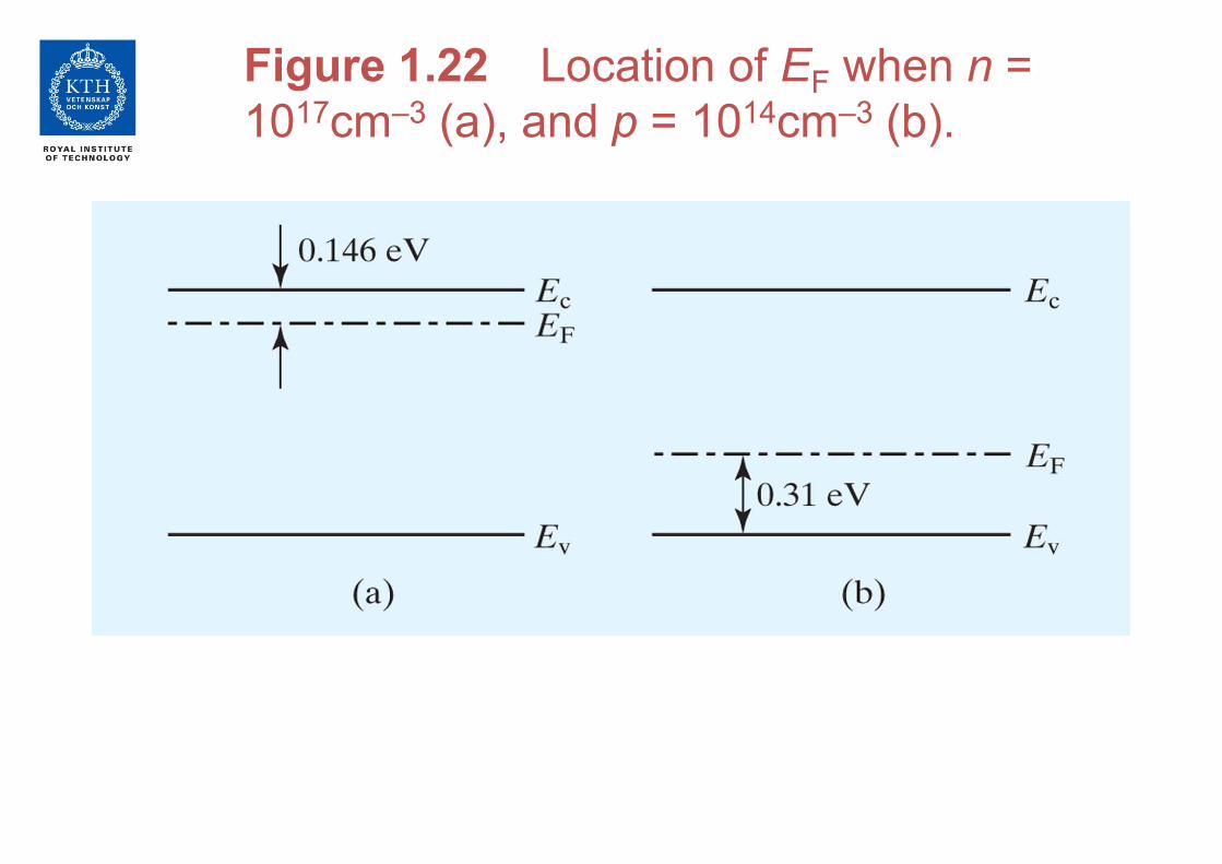
Figure 1.22 Location of EF when n = 1017cm–3 (a), and p = 1014cm–3 (b).
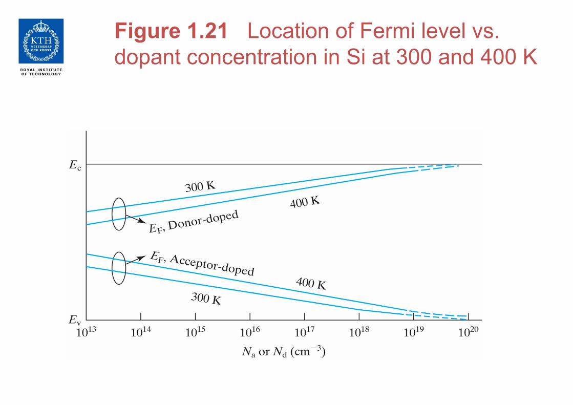
Figure 1.21 Location of Fermi level vs. dopant concentration in Si at 300 and 400 K
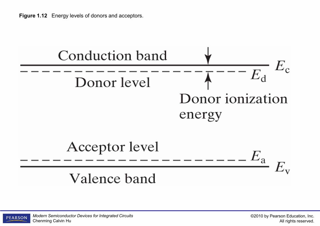
Donor/acceptor levels & temp dep.
©2010 by Pearson Education, Inc. All rights reserved.
Modern Semiconductor Devices for Integrated Circuits Chenming Calvin Hu
Figure 1.12 Energy levels of donors and acceptors.
©2010 by Pearson Education, Inc. All rights reserved.
Modern Semiconductor Devices for Integrated Circuits Chenming Calvin Hu
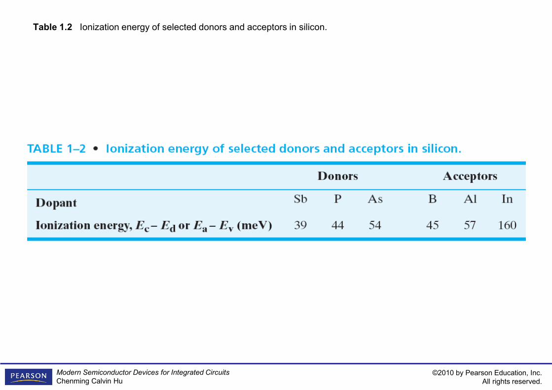
Table 1.2 Ionization energy of selected donors and acceptors in silicon.
©2010 by Pearson Education, Inc. All rights reserved.
Modern Semiconductor Devices for Integrated Circuits Chenming Calvin Hu
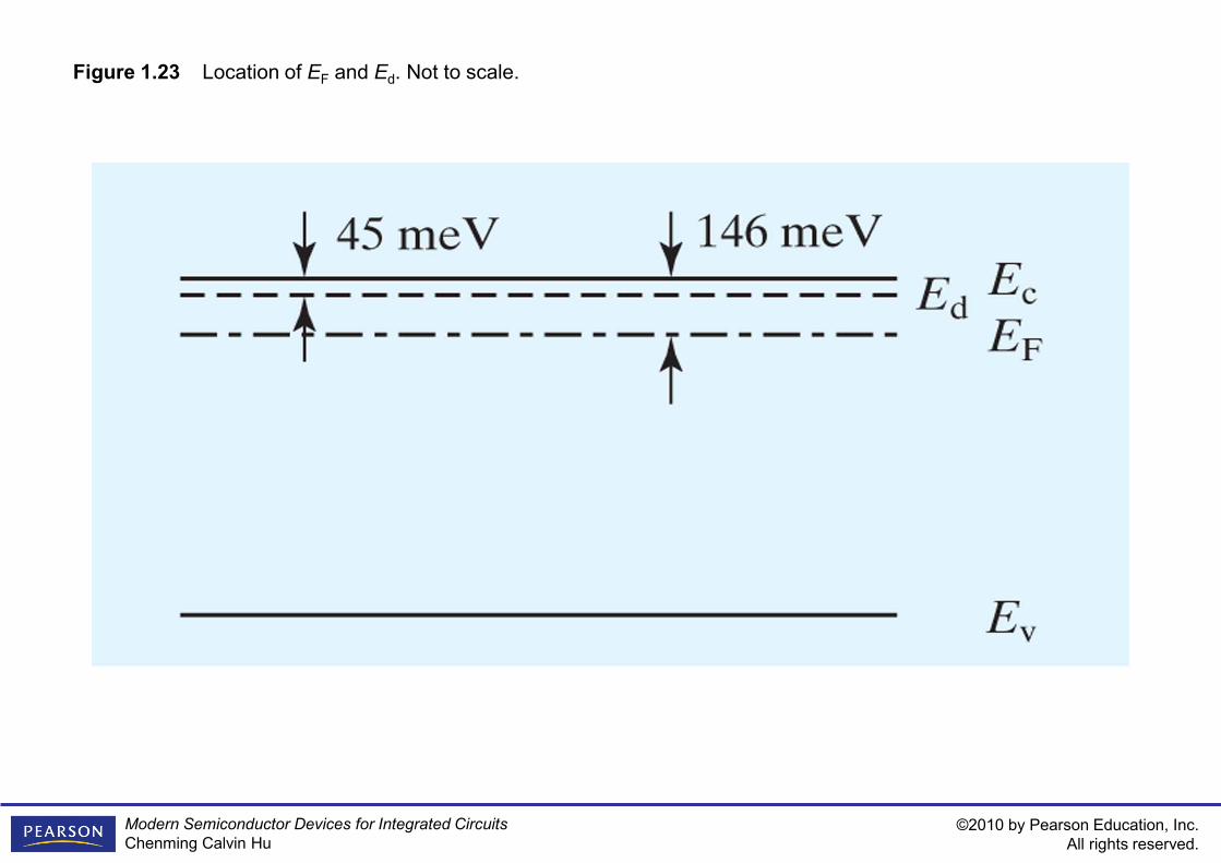
Figure 1.23 Location of EF and Ed. Not to scale.
©2010 by Pearson Education, Inc. All rights reserved.
Modern Semiconductor Devices for Integrated Circuits Chenming Calvin Hu
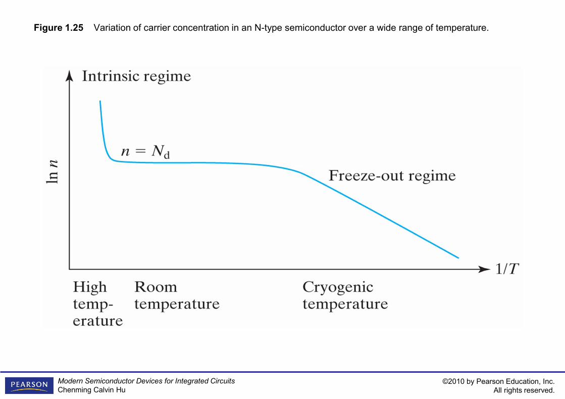
Figure 1.25 Variation of carrier concentration in an N-type semiconductor over a wide range of temperature.
Chapter 2
•Motion and Recombination of Electrons and Holes
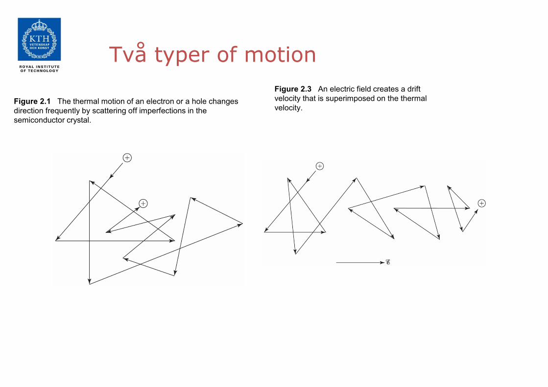
Två typer of motion
Figure 2.1 The thermal motion of an electron or a hole changes direction frequently by scattering off imperfections in the semiconductor crystal.
Figure 2.3 An electric field creates a drift velocity that is superimposed on the thermal velocity.
©2010 by Pearson Education, Inc. All rights reserved.
Modern Semiconductor Devices for Integrated Circuits Chenming Calvin Hu
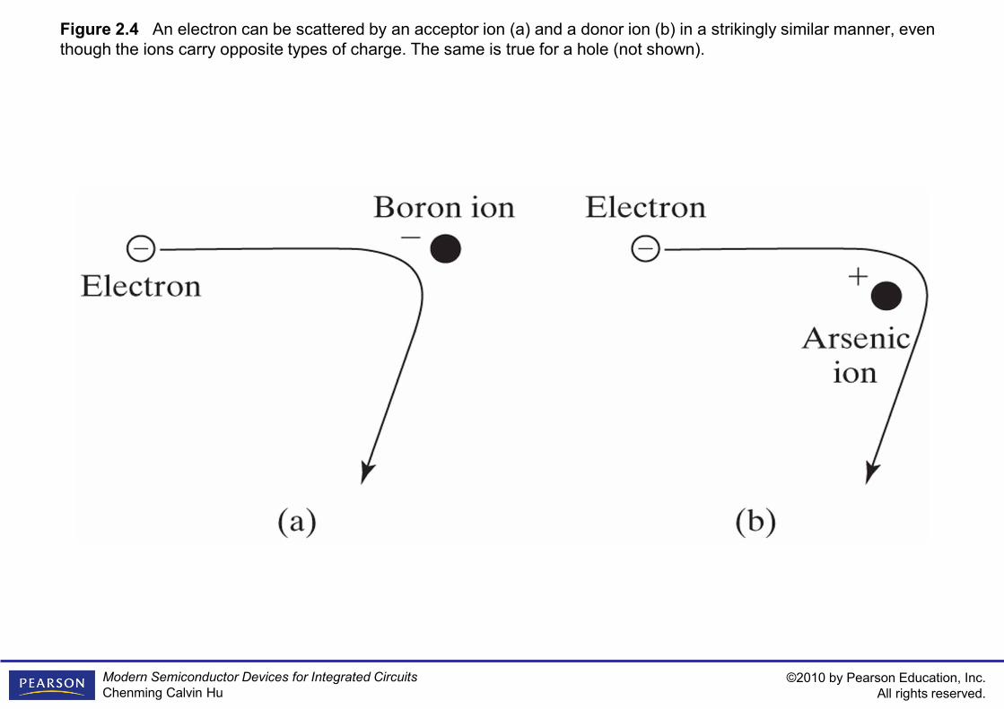
Figure 2.4 An electron can be scattered by an acceptor ion (a) and a donor ion (b) in a strikingly similar manner, even though the ions carry opposite types of charge. The same is true for a hole (not shown).
©2010 by Pearson Education, Inc. All rights reserved.
Modern Semiconductor Devices for Integrated Circuits Chenming Calvin Hu
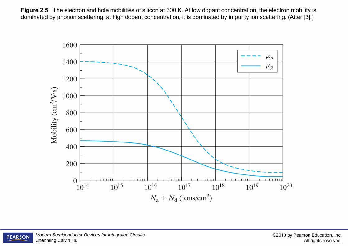
Figure 2.5 The electron and hole mobilities of silicon at 300 K. At low dopant concentration, the electron mobility is dominated by phonon scattering; at high dopant concentration, it is dominated by impurity ion scattering. (After [3].)
©2010 by Pearson Education, Inc. All rights reserved.
Modern Semiconductor Devices for Integrated Circuits Chenming Calvin Hu
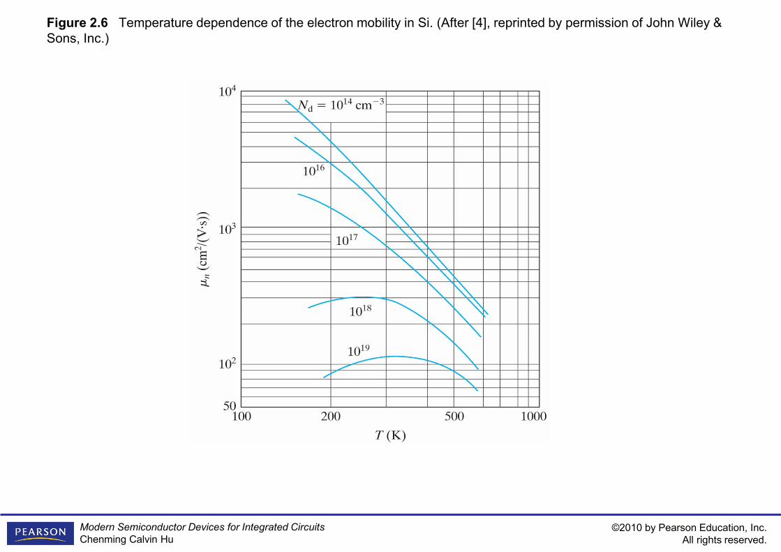
Figure 2.6 Temperature dependence of the electron mobility in Si. (After [4], reprinted by permission of John Wiley & Sons, Inc.)
©2010 by Pearson Education, Inc. All rights reserved.
Modern Semiconductor Devices for Integrated Circuits Chenming Calvin Hu
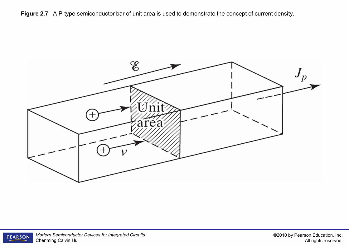
Figure 2.7 A P-type semiconductor bar of unit area is used to demonstrate the concept of current density.
©2010 by Pearson Education, Inc. All rights reserved.
Modern Semiconductor Devices for Integrated Circuits Chenming Calvin Hu
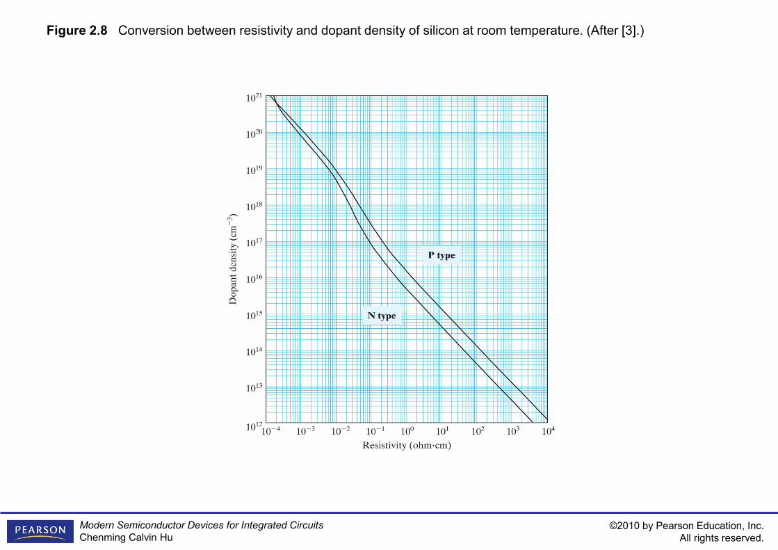
Figure 2.8 Conversion between resistivity and dopant density of silicon at room temperature. (After [3].)
©2010 by Pearson Education, Inc. All rights reserved.
Modern Semiconductor Devices for Integrated Circuits Chenming Calvin Hu
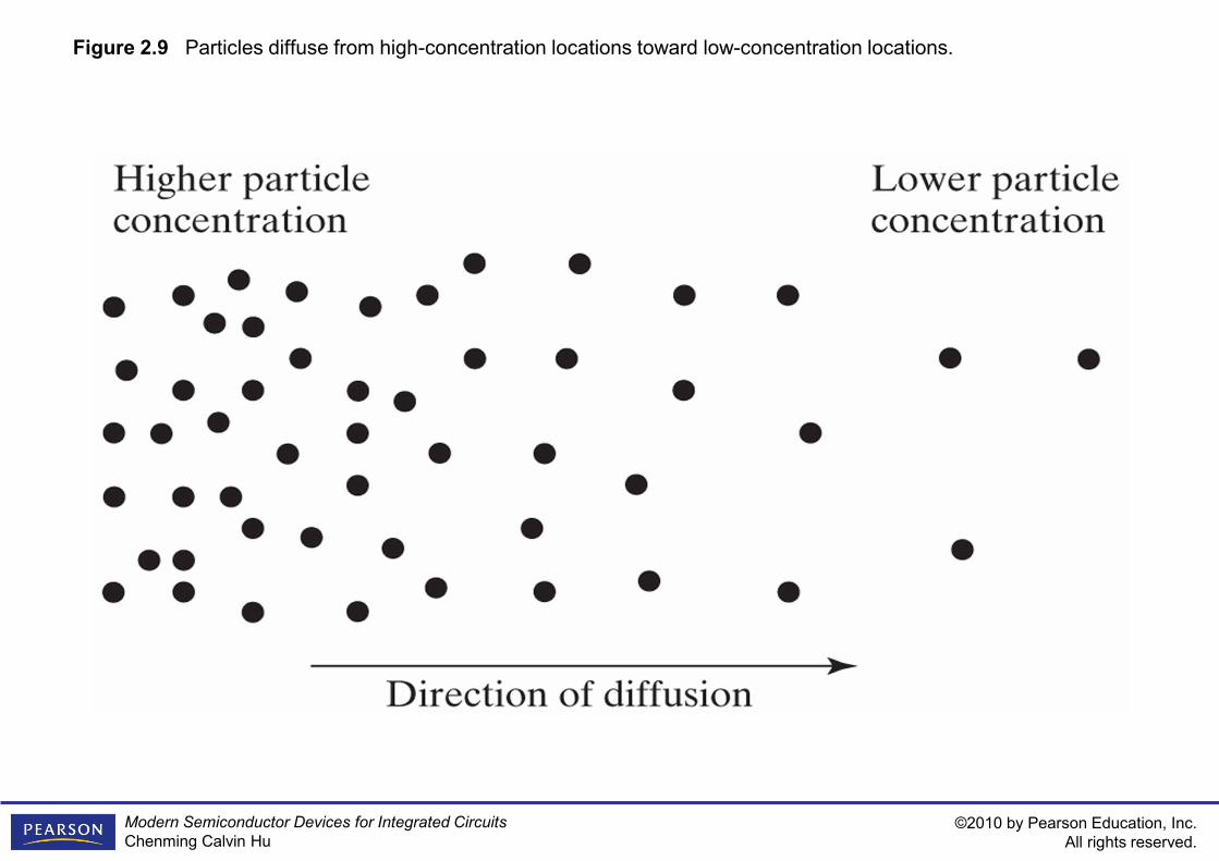
Figure 2.9 Particles diffuse from high-concentration locations toward low-concentration locations.
©2010 by Pearson Education, Inc. All rights reserved.
Modern Semiconductor Devices for Integrated Circuits Chenming Calvin Hu
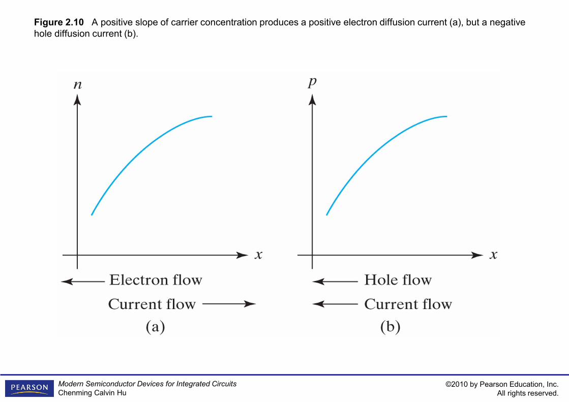
Figure 2.10 A positive slope of carrier concentration produces a positive electron diffusion current (a), but a negative hole diffusion current (b).
©2010 by Pearson Education, Inc. All rights reserved.
Modern Semiconductor Devices for Integrated Circuits Chenming Calvin Hu
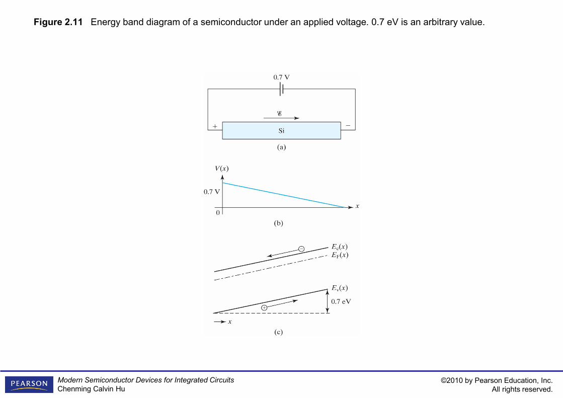
Figure 2.11 Energy band diagram of a semiconductor under an applied voltage. 0.7 eV is an arbitrary value.
©2010 by Pearson Education, Inc. All rights reserved.
Modern Semiconductor Devices for Integrated Circuits Chenming Calvin Hu
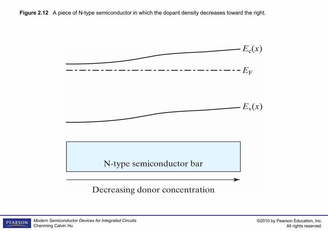
Figure 2.12 A piece of N-type semiconductor in which the dopant density decreases toward the right.
©2010 by Pearson Education, Inc. All rights reserved.
Modern Semiconductor Devices for Integrated Circuits Chenming Calvin Hu
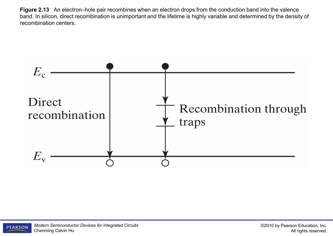
Figure 2.13 An electron–hole pair recombines when an electron drops from the conduction band into the valence band. In silicon, direct recombination is unimportant and the lifetime is highly variable and determined by the density of recombination centers.
©2010 by Pearson Education, Inc. All rights reserved.
Modern Semiconductor Devices for Integrated Circuits Chenming Calvin Hu
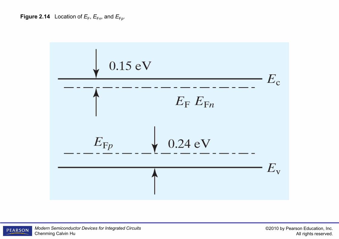
Figure 2.14 Location of EF, EFn, and EFp.
©2010 by Pearson Education, Inc. All rights reserved.
Modern Semiconductor Devices for Integrated Circuits Chenming Calvin Hu
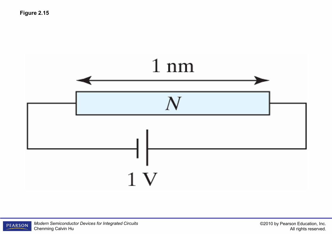
Figure 2.15
©2010 by Pearson Education, Inc. All rights reserved.
Modern Semiconductor Devices for Integrated Circuits Chenming Calvin Hu
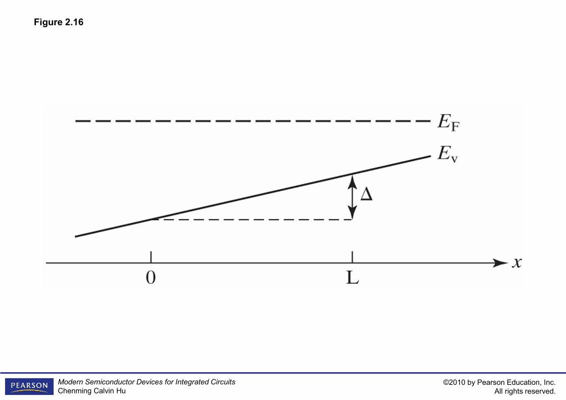
Figure 2.16