Embed Size (px)
Citation preview
Sequential circuits
part 2: implementation, analysis & design
All illustrations 2009-2010, Jones & Bartlett Publishers LLC, (www.jbpub.com)

More summer fashion
• SR is one of 4 basic flip flops common in computer design
• Others can all be constructed from SR; they are:– JK (don’t know why it’s called that)– D (data)– T (toggle)
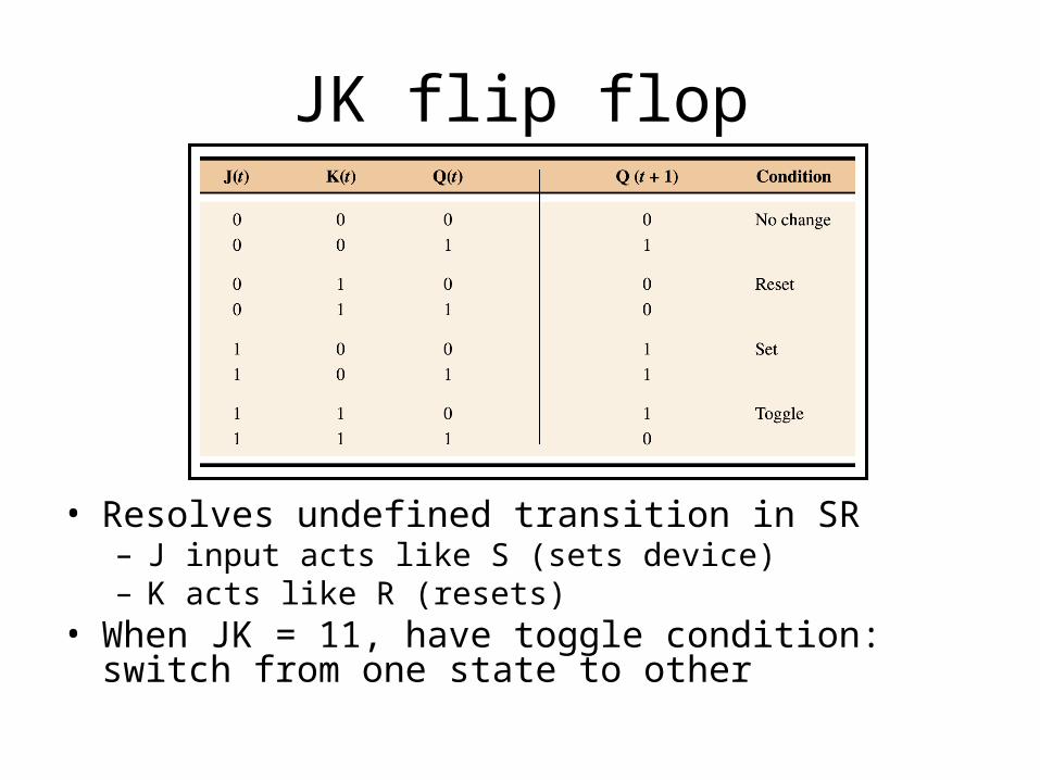
JK flip flop
• Resolves undefined transition in SR– J input acts like S (sets device)– K acts like R (resets)
• When JK = 11, have toggle condition: switch from one state to other
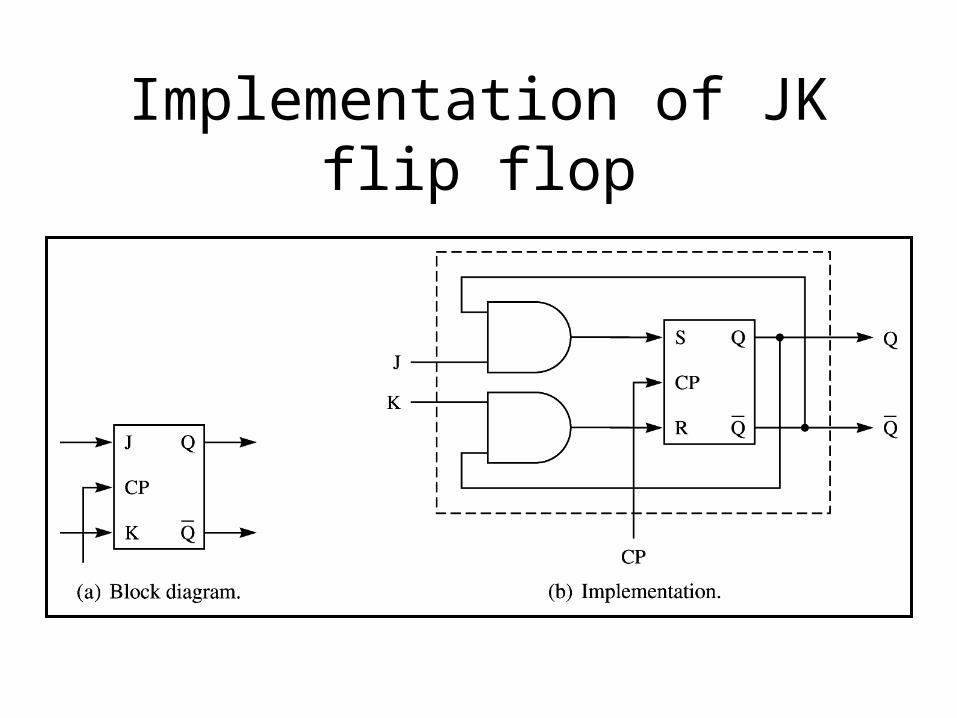
Implementation of JK flip flop
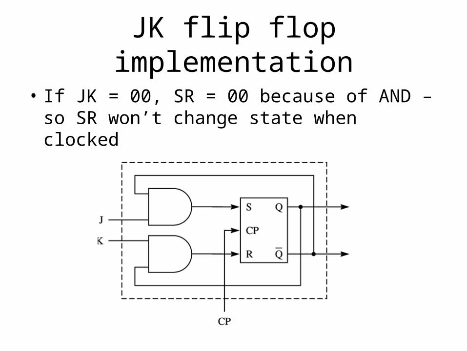
JK flip flop implementation
• If JK = 00, SR = 00 because of AND – so SR won’t change state when clocked
JK flip flop implementation
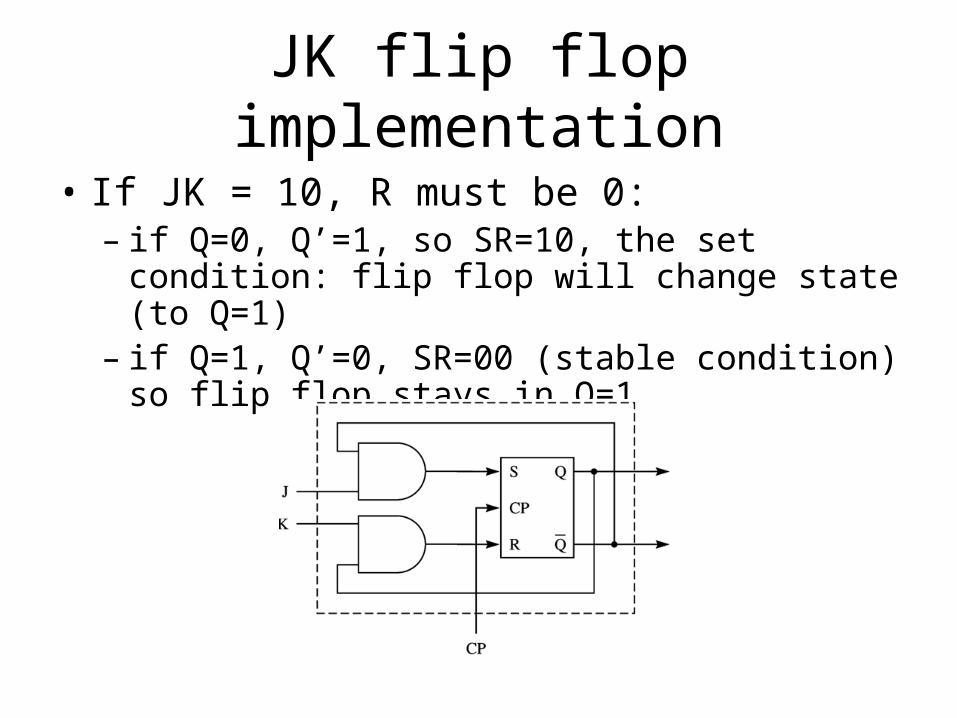
• If JK = 10, R must be 0:– if Q=0, Q’=1, so SR=10, the set condition: flip flop
will change state (to Q=1)– if Q=1, Q’=0, SR=00 (stable condition) so flip flop
stays in Q=1
JK flip flop implementation
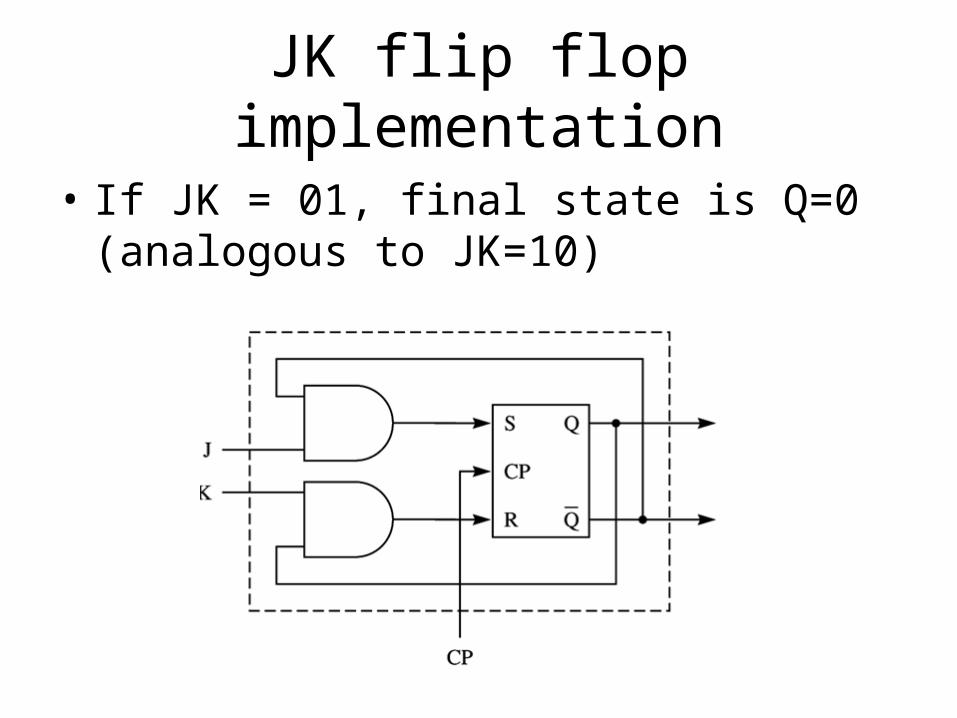
• If JK = 01, final state is Q=0 (analogous to JK=10)
JK flip flop implementation
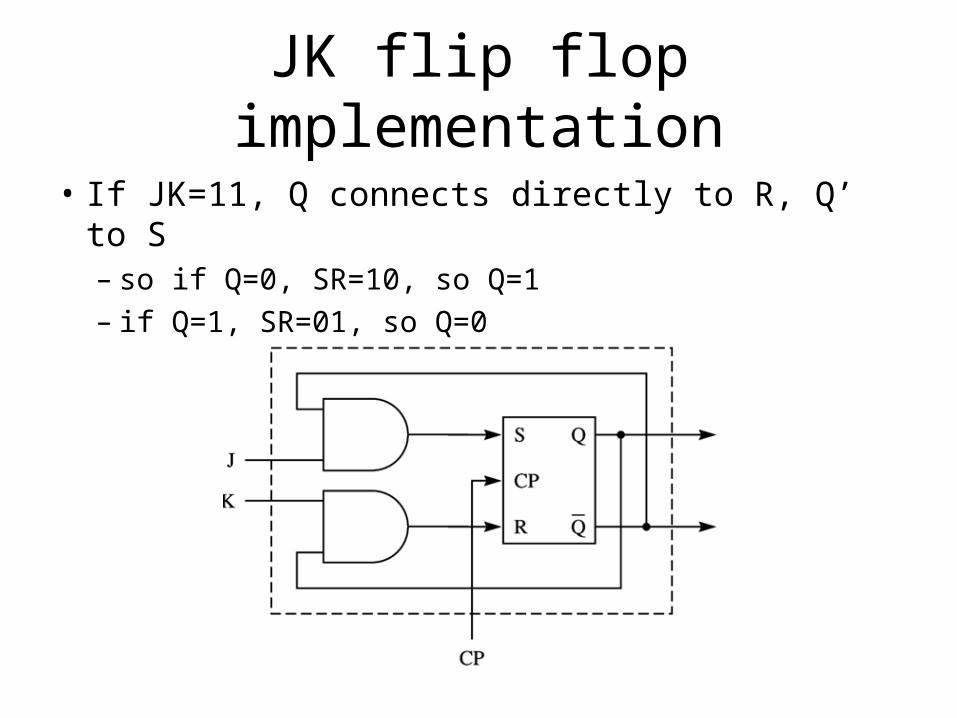
• If JK=11, Q connects directly to R, Q’ to S– so if Q=0, SR=10, so Q=1– if Q=1, SR=01, so Q=0
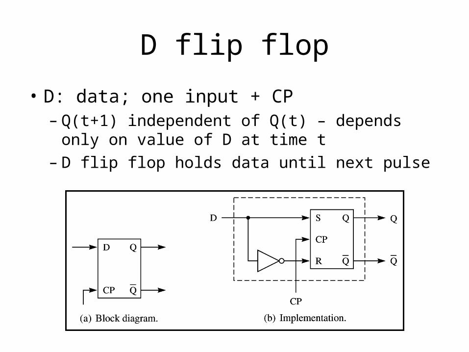
D flip flop
• D: data; one input + CP– Q(t+1) independent of Q(t) – depends only on
value of D at time t– D flip flop holds data until next pulse
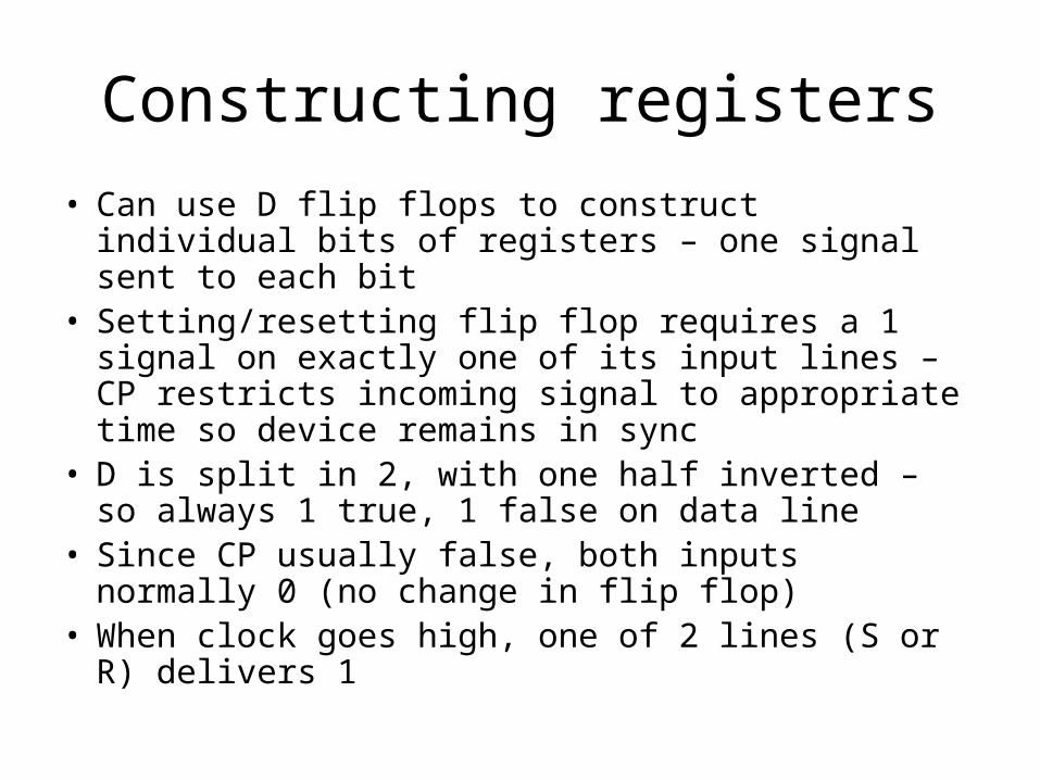
Constructing registers
• Can use D flip flops to construct individual bits of registers – one signal sent to each bit
• Setting/resetting flip flop requires a 1 signal on exactly one of its input lines – CP restricts incoming signal to appropriate time so device remains in sync
• D is split in 2, with one half inverted – so always 1 true, 1 false on data line
• Since CP usually false, both inputs normally 0 (no change in flip flop)
• When clock goes high, one of 2 lines (S or R) delivers 1
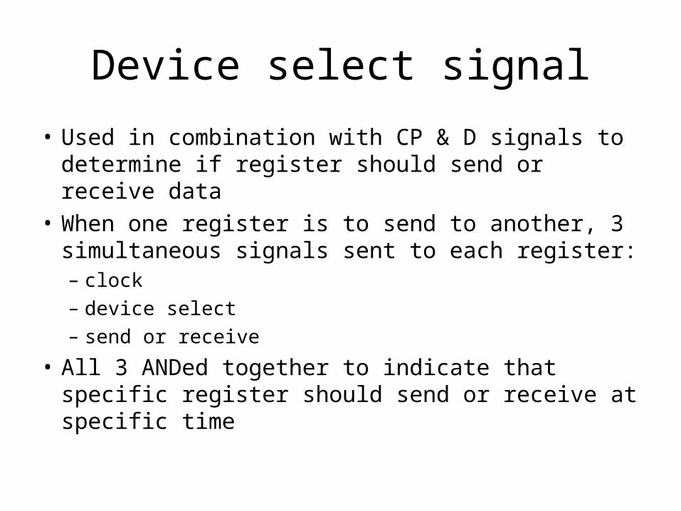
Device select signal
• Used in combination with CP & D signals to determine if register should send or receive data
• When one register is to send to another, 3 simultaneous signals sent to each register:– clock– device select– send or receive
• All 3 ANDed together to indicate that specific register should send or receive at specific time
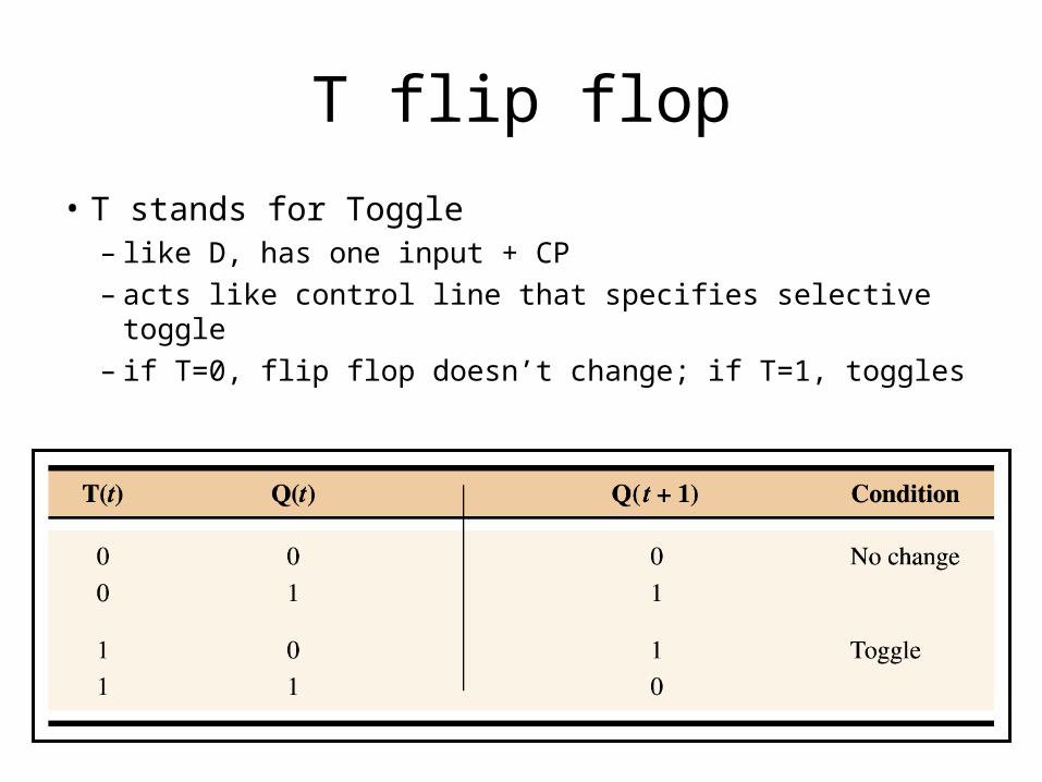
T flip flop
• T stands for Toggle– like D, has one input + CP– acts like control line that specifies selective toggle– if T=0, flip flop doesn’t change; if T=1, toggles
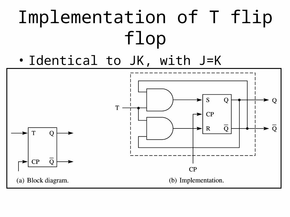
Implementation of T flip flop
• Identical to JK, with J=K
General sequential network
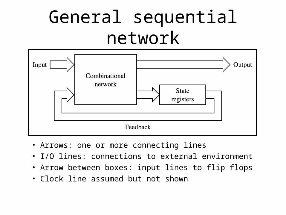
• Sequential circuit: interconnection of gates & flip flops
• All gates can be grouped conceptually as combinational network, all flip flops as group of state registers
• Between clock pulses, combinational part produces output; amount of time needed depends on number of gates in net
General sequential network
• Arrows: one or more connecting lines• I/O lines: connections to external environment• Arrow between boxes: input lines to flip flops• Clock line assumed but not shown
Hardware analysis vs. design
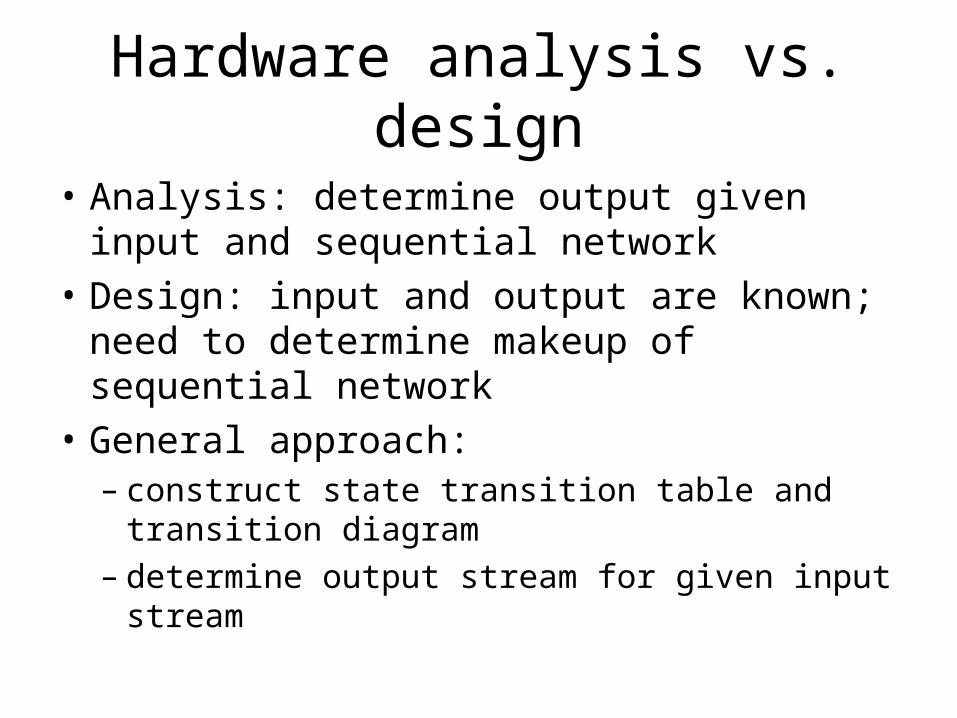
• Analysis: determine output given input and sequential network
• Design: input and output are known; need to determine makeup of sequential network
• General approach:– construct state transition table and transition
diagram– determine output stream for given input stream
Excitation table
• The excitation table is a design tool for constructing circuits from a given type of flip-flop
• Given the desired transition from Q(t) to Q(t +1), what inputs are necessary to make the transition happen?
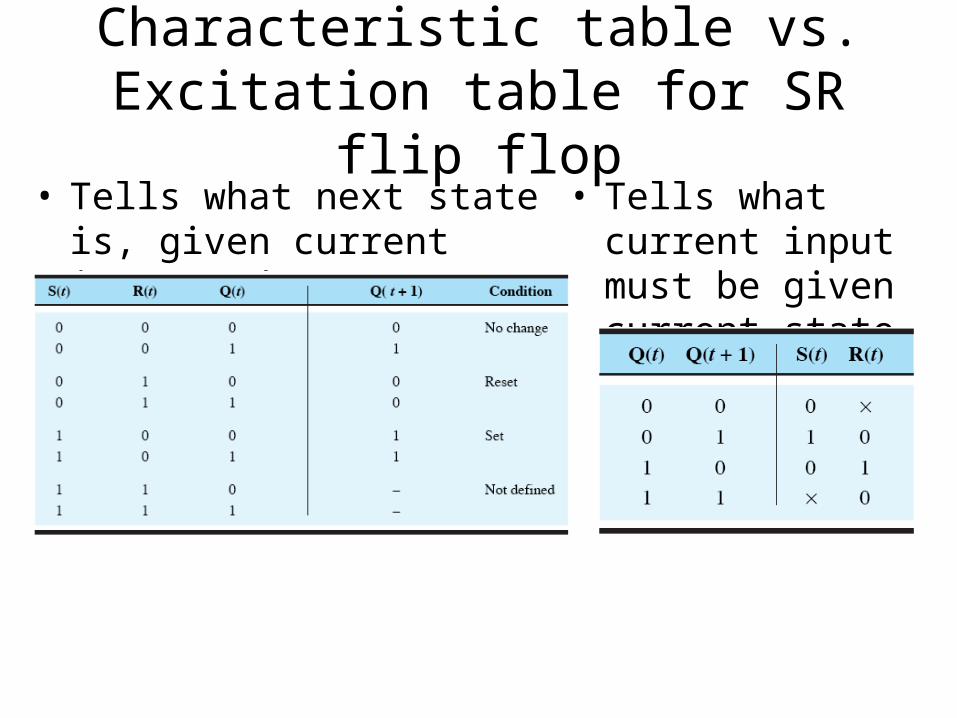
Characteristic table vs. Excitation table for SR flip flop
• Tells what next state is, given current input and current state
• Tells what current input must be given current state
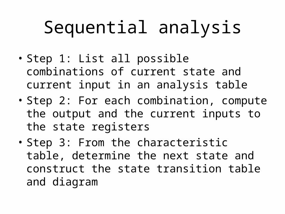
Sequential analysis
• Step 1: List all possible combinations of current state and current input in an analysis table
• Step 2: For each combination, compute the output and the current inputs to the state registers
• Step 3: From the characteristic table, determine the next state and construct the state transition table and diagram
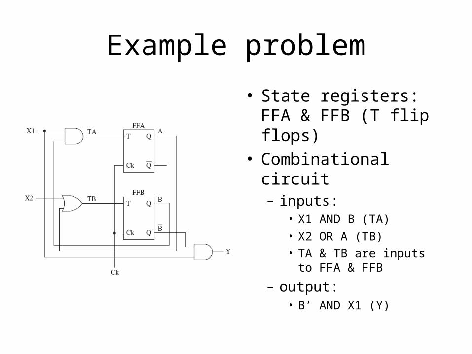
Example problem
• State registers: FFA & FFB (T flip flops)
• Combinational circuit– inputs:
• X1 AND B (TA)• X2 OR A (TB)• TA & TB are inputs to FFA
& FFB
– output:• B’ AND X1 (Y)
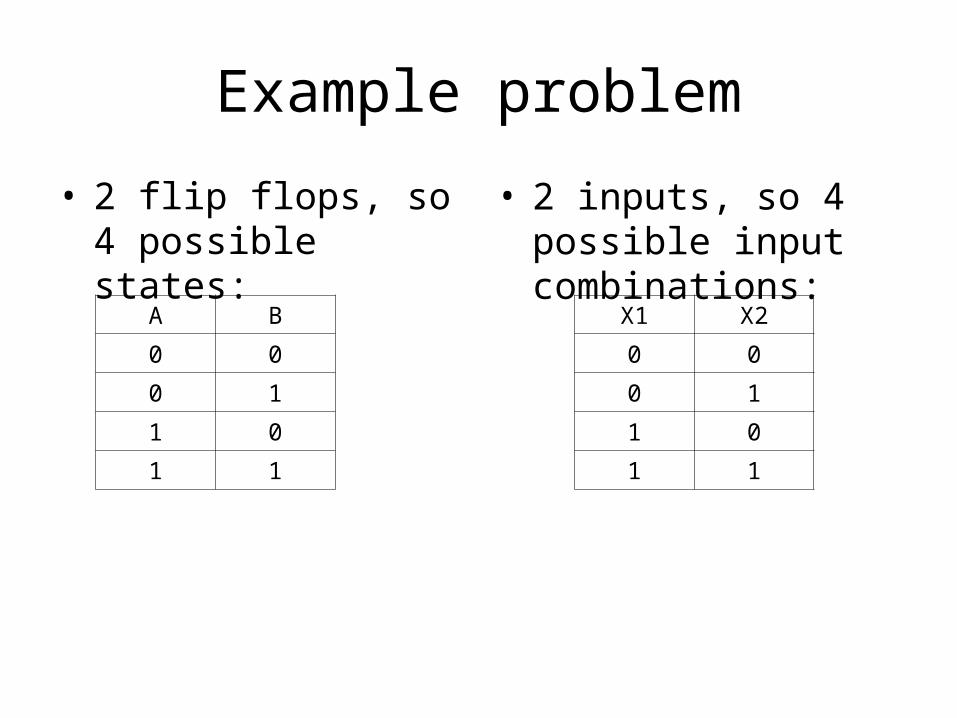
Example problem
• 2 flip flops, so 4 possible states:
A B
0 0
0 1
1 0
1 1
• 2 inputs, so 4 possible input combinations:
X1 X2
0 0
0 1
1 0
1 1
Example problem
• Given a state (AB) and an input (X1X2):– what is output?– what will be the state after CP?
• 16 possible answers, as shown on next slide
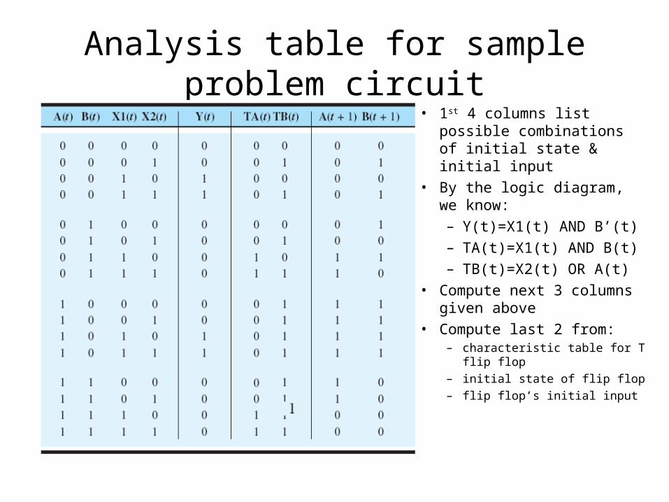
Analysis table for sample problem circuit• 1st 4 columns list possible
combinations of initial state & initial input
• By the logic diagram, we know:– Y(t)=X1(t) AND B’(t)– TA(t)=X1(t) AND B(t)– TB(t)=X2(t) OR A(t)
• Compute next 3 columns given above
• Compute last 2 from: – characteristic table for T flip
flop– initial state of flip flop– flip flop’s initial input
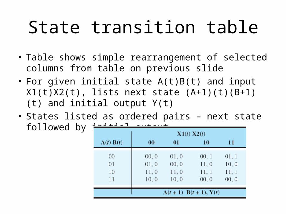
State transition table
• Table shows simple rearrangement of selected columns from table on previous slide
• For given initial state A(t)B(t) and input X1(t)X2(t), lists next state (A+1)(t)(B+1)(t) and initial output Y(t)
• States listed as ordered pairs – next state followed by initial output
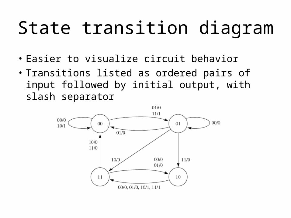
State transition diagram
• Easier to visualize circuit behavior• Transitions listed as ordered pairs of input
followed by initial output, with slash separator
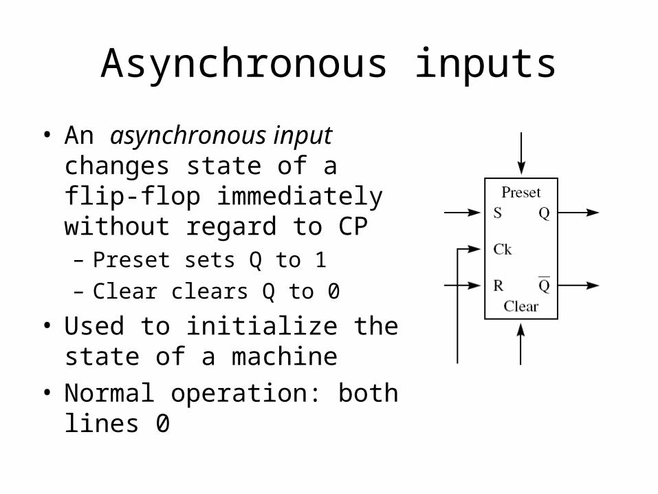
Asynchronous inputs
• An asynchronous input changes state of a flip-flop immediately without regard to CP– Preset sets Q to 1– Clear clears Q to 0
• Used to initialize the state of a machine
• Normal operation: both lines 0
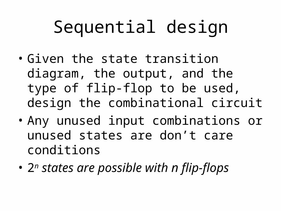
Sequential design
• Given the state transition diagram, the output, and the type of flip-flop to be used, design the combinational circuit
• Any unused input combinations or unused states are don’t care conditions
• 2n states are possible with n flip-flops
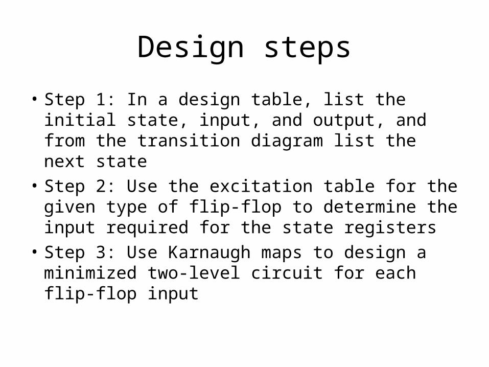
Design steps
• Step 1: In a design table, list the initial state, input, and output, and from the transition diagram list the next state
• Step 2: Use the excitation table for the given type of flip-flop to determine the input required for the state registers
• Step 3: Use Karnaugh maps to design a minimized two-level circuit for each flip-flop input
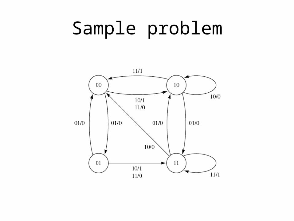
Sample problem
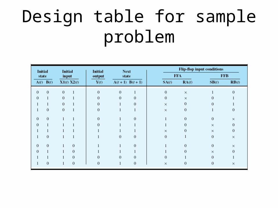
Design table for sample problem
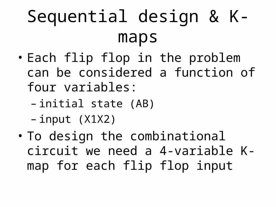
Sequential design & K-maps
• Each flip flop in the problem can be considered a function of four variables:– initial state (AB)– input (X1X2)
• To design the combinational circuit we need a 4-variable K-map for each flip flop input
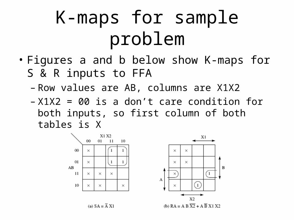
K-maps for sample problem
• Figures a and b below show K-maps for S & R inputs to FFA– Row values are AB, columns are X1X2– X1X2 = 00 is a don’t care condition for both inputs,
so first column of both tables is X
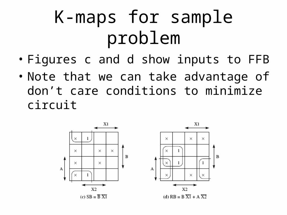
K-maps for sample problem
• Figures c and d show inputs to FFB• Note that we can take advantage of don’t care
conditions to minimize circuit
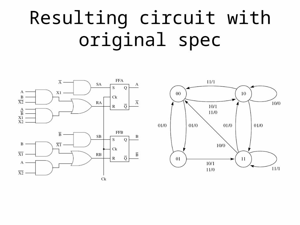
Resulting circuit with original spec
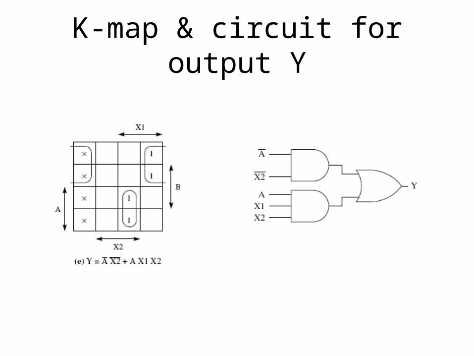
K-map & circuit for output Y
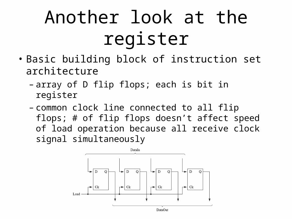
Another look at the register
• Basic building block of instruction set architecture– array of D flip flops; each is bit in register– common clock line connected to all flip flops; # of
flip flops doesn’t affect speed of load operation because all receive clock signal simultaneously
Memory
• Conceptually, main memory is just a big array of registers
• Input: address lines, control lines, data lines• Data lines are bidirectional (output also)• Control signals:
– CS: Chip select, to enable or select the memory chip– WE: Write enable, to write or store a memory word to the
chip– OE: Output enable, to enable the output buffer to read a
word from the chip
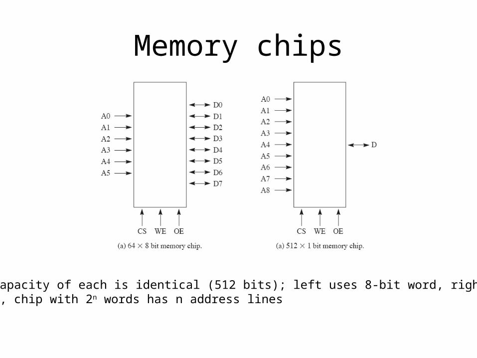
Memory chips
Storage capacity of each is identical (512 bits); left uses 8-bit word, right uses 1Generally, chip with 2n words has n address lines
Memory access
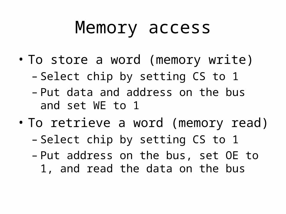
• To store a word (memory write)– Select chip by setting CS to 1– Put data and address on the bus and set WE to 1
• To retrieve a word (memory read)– Select chip by setting CS to 1– Put address on the bus, set OE to 1, and read the
data on the bus
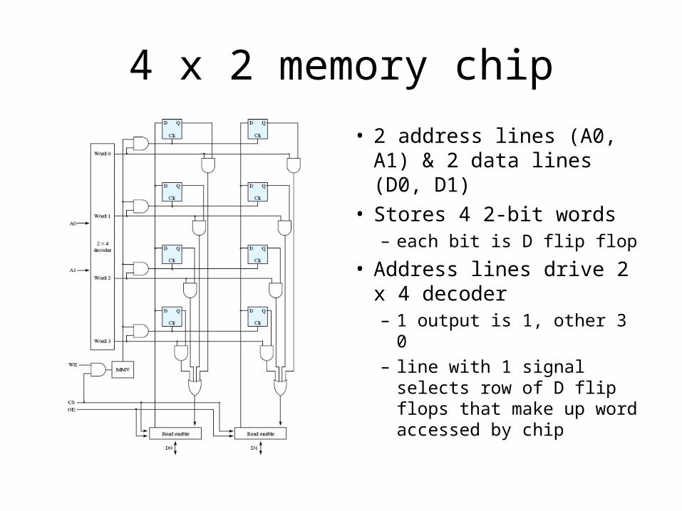
4 x 2 memory chip
• 2 address lines (A0, A1) & 2 data lines (D0, D1)
• Stores 4 2-bit words– each bit is D flip flop
• Address lines drive 2 x 4 decoder– 1 output is 1, other 3 0– line with 1 signal selects
row of D flip flops that make up word accessed by chip
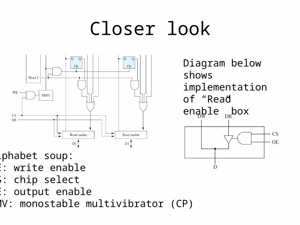
Closer look
Diagram below shows implementation of “Read enable” box
Alphabet soup:WE: write enableCS: chip selectOE: output enableMMV: monostable multivibrator (CP)
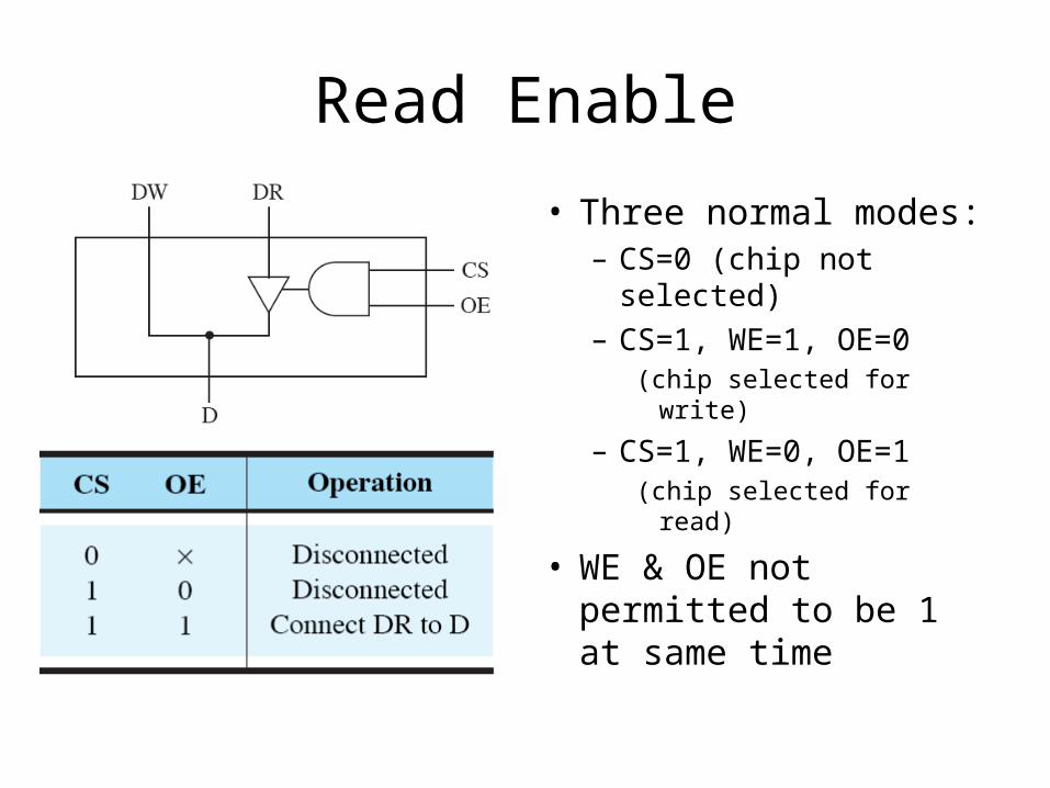
Read Enable
• Three normal modes:– CS=0 (chip not selected)– CS=1, WE=1, OE=0
(chip selected for write)
– CS=1, WE=0, OE=1(chip selected for read)
• WE & OE not permitted to be 1 at same time
Memory types: volatile
• SRAM: Static random access memory– most closely resembles model we’ve seen– advantage: fast– disadvantage: large – several transistors required for each
bit cell
• DRAM: Dynamic RAM– overcomes size problem of SRAM: one transistor, one
capacitor per cell– advantage: high capacity– disadvantage: relatively slow because requires refresh
operation
Memory types: non-volatile
• ROM: Read-only memory– Simplest type, ROM, is prewritten to spec by
manufacturer – can’t be overwritten– PROM: Programmable ROM: user can write once
(by blowing embedded fuses) – can’t be overwritten
– EPROM: Erasable PROM: can be wiped out & reprogrammed (requires removal from computer)
Memory types: non-volatile
• EEPROM: Electrically erasable PROM– Like EPROM, but doesn’t require removal to
reprogram– Can reprogram individual cell (doesn’t have to be
whole chip)
• Flash memory: A type of EEPROM– flash card is array of flash chips– flash drive has interface circuitry to mimic hard
drive