Embed Size (px)
Citation preview
RoHS Compliant
Serial ATA Flash Drive mSATA H1-M Product Specifications
November 20th
, 2014
Version 1.3
Apacer Technology Inc.
1F, No.32, Zhongcheng Rd., Tucheng Dist., New Taipei City, Taiwan, R.O.C
Tel: +886-2-2267-8000 Fax: +886-2-2267-2261
www.apacer.com
http://www.apacer.com
http://www.apacer.com
Serial ATA Flash Drive APSDMxxxxM1HN-XTMX
1 © 2014 Apacer Technology Inc. Rev. 1.3
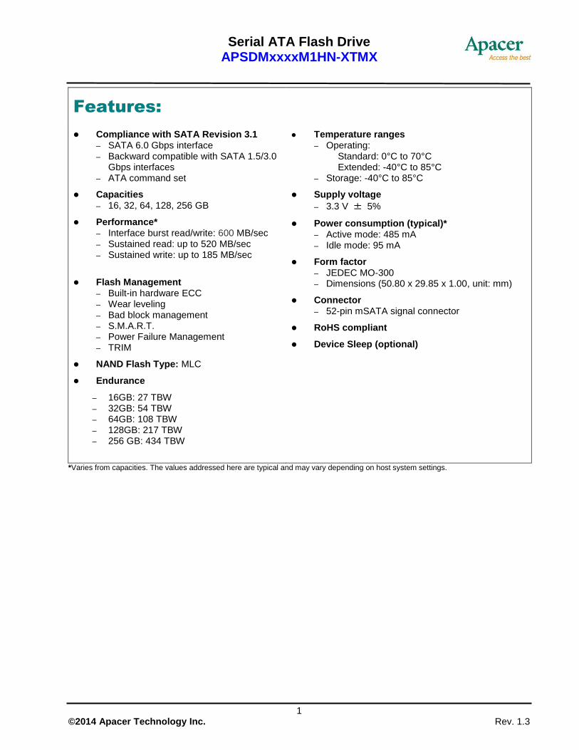
Features:
Compliance with SATA Revision 3.1 – SATA 6.0 Gbps interface – Backward compatible with SATA 1.5/3.0
Gbps interfaces – ATA command set
Capacities – 16, 32, 64, 128, 256 GB
Performance* – Interface burst read/write: 600 MB/sec – Sustained read: up to 520 MB/sec – Sustained write: up to 185 MB/sec
Flash Management – Built-in hardware ECC – Wear leveling – Bad block management – S.M.A.R.T. – Power Failure Management – TRIM
NAND Flash Type: MLC
Endurance
– 16GB: 27 TBW – 32GB: 54 TBW – 64GB: 108 TBW – 128GB: 217 TBW – 256 GB: 434 TBW
Temperature ranges – Operating: Standard: 0°C to 70°C Extended: -40°C to 85°C – Storage: -40°C to 85°C
Supply voltage
– 3.3 V ± 5%
Power consumption (typical)* – Active mode: 485 mA – Idle mode: 95 mA
Form factor – JEDEC MO-300 – Dimensions (50.80 x 29.85 x 1.00, unit: mm)
Connector – 52-pin mSATA signal connector
RoHS compliant
Device Sleep (optional)
*Varies from capacities. The values addressed here are typical and may vary depending on host system settings.
Serial ATA Flash Drive APSDMxxxxM1HN-XTMX
2 © 2014 Apacer Technology Inc. Rev. 1.3
Table of Contents
1. Product Description ............................................................................................... 3 1.1 Introduction ................................................................................................................................................... 3 1.2 Capacity Specification ................................................................................................................................... 3 1.3 Performance ................................................................................................................................................... 3 1.4 Pin Assignments ............................................................................................................................................. 4
2. Software Interface ................................................................................................... 6
2.1 Command Set ................................................................................................................................................. 6 2.2 S.M.A.R.T. ...................................................................................................................................................... 6
3. Flash Management ................................................................................................. 7
3.1 Error Correction/Detection .......................................................................................................................... 7 3.2 Bad Block Management ................................................................................................................................ 7 3.3 Wear Leveling ................................................................................................................................................ 7 3.4 Power Failure Management .......................................................................................................................... 7 3.5 TRIM .............................................................................................................................................................. 7 3.6 Secure Erase ................................................................................................................................................... 8
4. Environment Specifications .................................................................................. 9
4.1 Environmental ............................................................................................................................................... 9 4.2 Mean Time Between Failures (MTBF) ........................................................................................................ 9 4.3 Certification and Compliance ....................................................................................................................... 9 4.4 Endurance .................................................................................................................................................... 10
5. Electrical Characteristics ..................................................................................... 11 5.1 Operating Voltage ........................................................................................................................................ 11 5.2 Power Consumption .................................................................................................................................... 11
6. Mechanical Specifications ................................................................................... 12 6.1 Dimensions ................................................................................................................................................... 12
7. Product Ordering Information ............................................................................. 13
7.1 Product Code Designation........................................................................................................................... 13 7.2 Valid Combination....................................................................................................................................... 14
Serial ATA Flash Drive APSDMxxxxM1HN-XTMX
3 © 2014 Apacer Technology Inc. Rev. 1.3
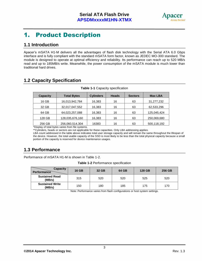
1. Product Description
1.1 Introduction
Apacer’s mSATA H1-M delivers all the advantages of flash disk technology with the Serial ATA 6.0 Gbps interface and is fully compliant with the standard mSATA form factor, known as JEDEC MO-300 standard. The module is designed to operate at optimal efficiency and reliability. Its performance can reach up to 520 MB/s read and up to 185MB/s write. Meanwhile, the power consumption of the mSATA module is much lower than traditional hard drives.
1.2 Capacity Specification
Table 1-1 Capacity specification
Capacity Total Bytes Cylinders Heads Sectors Max LBA
16 GB 16,013,942,784 16,383 16 63 31,277,232
32 GB 32,017,047,552 16,383 16 63 62,533,296
64 GB 64,023,257,088 16,383 16 63 125,045,424
128 GB 128,035,676,160 16,383 16 63 250,069,680
256 GB 256,060,514,304 16383 16 63 500,118,192 *Display of total bytes varies from file systems. **Cylinders, heads or sectors are not applicable for these capacities. Only LBA addressing applies. LBA count addressed in the table above indicates total user storage capacity and will remain the same throughout the lifespan of the device. However, the total usable capacity of the SSD is most likely to be less than the total physical capacity because a small portion of the capacity is reserved for device maintenance usages.
1.3 Performance
Performance of mSATA H1-M is shown in Table 1-2.
Table 1-2 Performance specification
Capacity Performance
16 GB 32 GB 64 GB 128 GB 256 GB
Sustained Read (MB/s)
315 520 520 525 520
Sustained Write (MB/s)
150 180 185 175 170
Note: Performance varies from flash configurations or host system settings.
Serial ATA Flash Drive APSDMxxxxM1HN-XTMX
4 © 2014 Apacer Technology Inc. Rev. 1.3
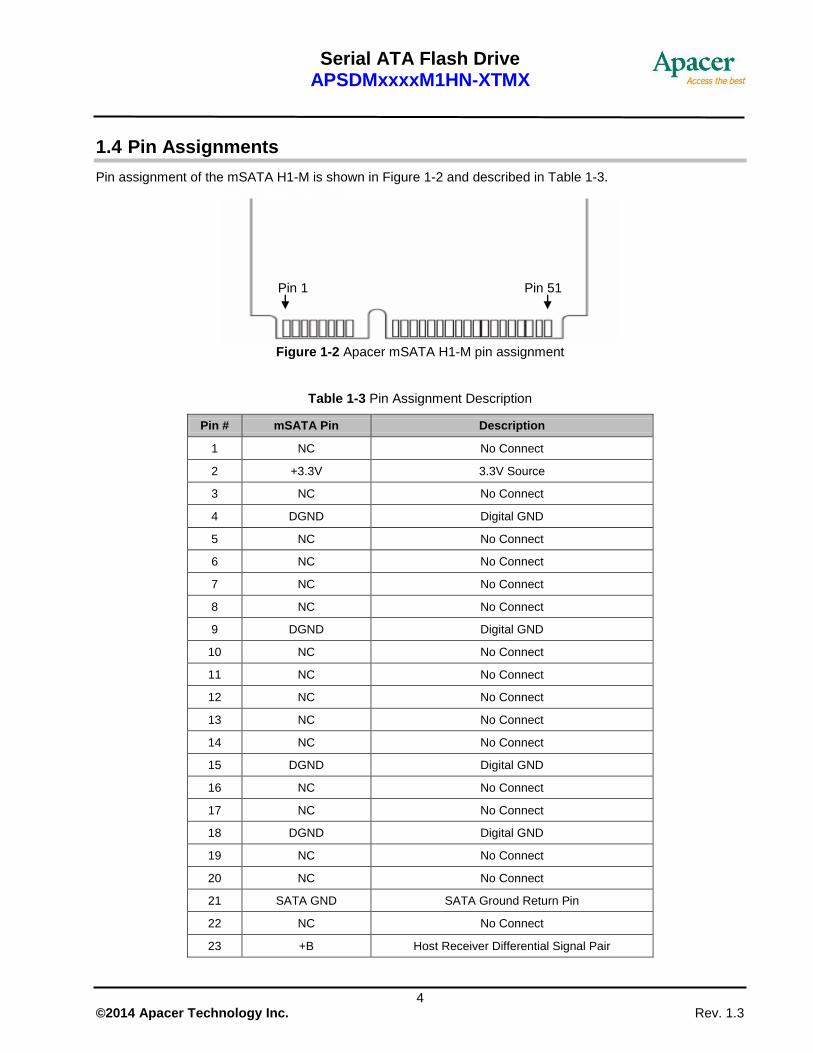
1.4 Pin Assignments
Pin assignment of the mSATA H1-M is shown in Figure 1-2 and described in Table 1-3.
Figure 1-2 Apacer mSATA H1-M pin assignment
Table 1-3 Pin Assignment Description
Pin # mSATA Pin Description
1 NC No Connect
2 +3.3V 3.3V Source
3 NC No Connect
4 DGND Digital GND
5 NC No Connect
6 NC No Connect
7 NC No Connect
8 NC No Connect
9 DGND Digital GND
10 NC No Connect
11 NC No Connect
12 NC No Connect
13 NC No Connect
14 NC No Connect
15 DGND Digital GND
16 NC No Connect
17 NC No Connect
18 DGND Digital GND
19 NC No Connect
20 NC No Connect
21 SATA GND SATA Ground Return Pin
22 NC No Connect
23 +B Host Receiver Differential Signal Pair
Pin 1 Pin 51
Serial ATA Flash Drive APSDMxxxxM1HN-XTMX
5 © 2014 Apacer Technology Inc. Rev. 1.3
24 +3.3V 3.3V Source
25 -B Host Receiver Differential Signal Pair
26 SATA GND SATA Ground Return Pin
27 SATA GND SATA Ground Return Pin
28 NC No Connect
29 SATA GND SATA Ground Return Pin
30 NC No Connect
31 -A Host Transmitter Differential Signal Pair
32 NC No Connect
33 +A Host Transmitter Differential Signal Pair
34 DGND Digital GND
35 SATA GND SATA Ground Return Pin
36 NC No Connect
37 SATA GND SATA Ground Return Pin
38 NC No Connect
39 +3.3V 3.3V Source
40 DGND Digital GND
41 +3.3V 3.3V Source
42 NC No Connect
43 NC No Connect
44 NC No Connect
45 Vendor Vendor specific
46 NC No Connect
47 Vendor Vendor specific
48 NC No Connect
49 DA/DSS Device activity signal
50 DGND Digital GND
51 GND Default connect to GND
52 +3.3V 3.3V Source
Serial ATA Flash Drive APSDMxxxxM1HN-XTMX
6 © 2014 Apacer Technology Inc. Rev. 1.3
2. Software Interface
2.1 Command Set
Table 2-1 summarizes the ATA commands supported by mSATA H1-M.
Table 2-1: Command set
Code Command Code Command
E5h Check power mode F6h Security Disable Password
06h Data Set management F3h Security Erase Prepare
B1H DCO F4h Security Erase Unit
92h Download Microcode PIO F5h Security Freeze Lock
93h Download Microcode DMA F1h Security Set Password
90h Execute drive diagnostic F2h Security Unlock
E7h Flush cache 70h Seek
Eah Flush cache Ext Efh Set features
Ech Identify device F9h Set Max Address
E3h Idle 37h Set Max Address Ext
E1h Idle immediate C6h Set multiple mode
91h Initialize drive parameters E6h Sleep
E4h Read buffer B0h Smart
C9h Read DMA (w/o retry) E2h Standby
C8h Read DMA (w/retry) E0h Standby immediate
25h Read DMA Ext E8h Write buffer
60h Read FPDMA QUEUED CBh Write DMA (w/o retry)
2Fh Read Log Ext Cah Write DMA (w/retry)
C4h Read multiple 35h Write DMA Ext
29h Read multiple Ext 3Dh Write DMA FUA Ext
F8h Read native max address 61h Write FPDMA QUEUED
27h Read native max Ext 3Fh Write Log Ext
21h Read sector(s) (w/o retry) C5h Write multiple
20h Read sector(s) (w/retry) 39h Write multiple Ext
24h Read sector(s) Ext Ceh Write multiple FUA Ext
42h Read Verify Ext 31h Write sector(s) (w/o retry)
41h Read verify sector(s) (w/o retry) 30h Write sector(s) (w/retry)
40h Read verify sector(s) (w/retry) 34h Write sector(s) Ext
10h Recalibrate 45h Write uncorrectable
Note. Security command will only be workable when device runs in non-OPAL compliant mode.
2.2 S.M.A.R.T.
SMART, an acronym for Self-Monitoring, Analysis and Reporting Technology, is an open standard that allows a hard disk drive to automatically detect its health and report potential failures. When a failure is recorded by SMART, users can choose to replace the drive to prevent unexpected outage or data loss. Moreover, SMART can inform users of impending failures while there is still time to perform proactive actions, such as copy data to another device.
Serial ATA Flash Drive APSDMxxxxM1HN-XTMX
7 © 2014 Apacer Technology Inc. Rev. 1.3
3. Flash Management
3.1 Error Correction/Detection
Flash memory cells will deteriorate with use, which might generate random bit errors in the stored data. Thus, this mSATA SSD module applies the BCH ECC Algorithm, which can detect and correct errors occur during Read process, ensure data been read correctly, as well as protect data from corruption. This device can correct up to 72bit/1K data.
3.2 Bad Block Management
Bad blocks are blocks that include one or more invalid bits, and their reliability is not guaranteed. Blocks that are identified and marked as bad by the manufacturer are referred to as “Initial Bad Blocks”. Bad blocks that are developed during the lifespan of the flash are named “Later Bad Blocks”. Apacer implements an efficient bad block management algorithm to detect the factory-produced bad blocks and manages any bad blocks that appear with use. This practice further prevents data being stored into bad blocks and improves the data reliability.
3.3 Wear Leveling
NAND Flash devices can only undergo a limited number of program/erase cycles, and in most cases, the flash media are not used evenly. If some areas get updated more frequently than others, the lifetime of the device would be reduced significantly. Thus, Wear Leveling technique is applied to extend the lifespan of NAND Flash by evenly distributing write and erase cycles across the media.
Apacer provides advanced Wear Leveling algorithm, which can efficiently spread out the flash usage through the whole flash media area. Moreover, by implementing both dynamic and static Wear Leveling algorithms, the life expectancy of the NAND Flash is greatly improved.
3.4 Power Failure Management
Power Failure Management plays a crucial role when experiencing unstable power supply. Power disruption may occur when users are storing data into the SSD. In this urgent situation, the controller would run multiple flush cycles to store the metadata for later block rebuilding. This urgent operation requires about several milliseconds to get it done. At the next power up, the firmware will perform a status tracking to retrieve the mapping table and resume previously programmed NAND blocks to check if there is any incompleteness of transmission.
3.5 TRIM
TRIM is a feature which helps improve the read/write performance and speed of solid-state drives (SSD). Unlike hard disk drives (HDD), SSDs are not able to overwrite existing data, so the available space gradually becomes smaller with each use. With the TRIM command, the operating system can inform the SSD which blocks of data are no longer in use and can be removed permanently. Thus, the SSD will perform the erase action, which prevents unused data from occupying blocks all the time.
Serial ATA Flash Drive APSDMxxxxM1HN-XTMX
8 © 2014 Apacer Technology Inc. Rev. 1.3
3.6 Secure Erase
Secure Erase is a standard ATA command and will write all “0xFF” to fully wipe all the data on hard drives and SSDs. When this command is issued, the SSD controller will empty its storage blocks and return to its factory default settings.
Note. Secure erase command belongs to ATA security command.
Serial ATA Flash Drive APSDMxxxxM1HN-XTMX
9 © 2014 Apacer Technology Inc. Rev. 1.3
4. Environment Specifications
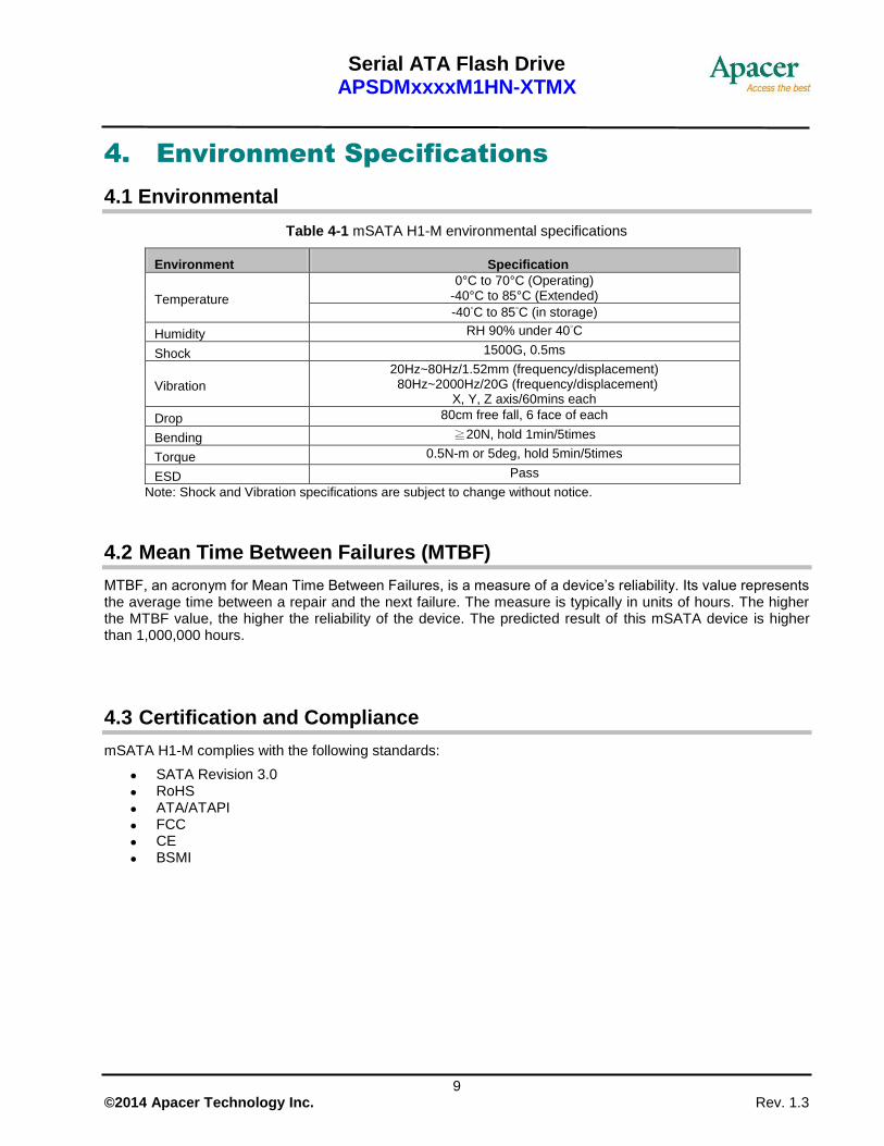
4.1 Environmental
Table 4-1 mSATA H1-M environmental specifications
Environment Specification
Temperature
0°C to 70°C (Operating) -40°C to 85°C (Extended)
-40°C to 85°C (in storage)
Humidity RH 90% under 40°C
Shock 1500G, 0.5ms
Vibration
20Hz~80Hz/1.52mm (frequency/displacement) 80Hz~2000Hz/20G (frequency/displacement)
X, Y, Z axis/60mins each
Drop 80cm free fall, 6 face of each
Bending ≧20N, hold 1min/5times
Torque 0.5N-m or 5deg, hold 5min/5times
ESD Pass
Note: Shock and Vibration specifications are subject to change without notice.
4.2 Mean Time Between Failures (MTBF)
MTBF, an acronym for Mean Time Between Failures, is a measure of a device’s reliability. Its value represents the average time between a repair and the next failure. The measure is typically in units of hours. The higher the MTBF value, the higher the reliability of the device. The predicted result of this mSATA device is higher than 1,000,000 hours.
4.3 Certification and Compliance
mSATA H1-M complies with the following standards:
SATA Revision 3.0 RoHS ATA/ATAPI FCC CE BSMI
Serial ATA Flash Drive APSDMxxxxM1HN-XTMX
10 © 2014 Apacer Technology Inc. Rev. 1.3
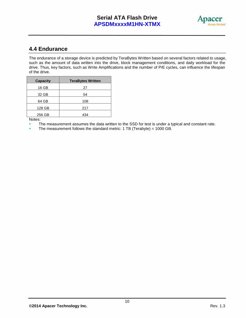
4.4 Endurance
The endurance of a storage device is predicted by TeraBytes Written based on several factors related to usage, such as the amount of data written into the drive, block management conditions, and daily workload for the drive. Thus, key factors, such as Write Amplifications and the number of P/E cycles, can influence the lifespan of the drive.
Capacity TeraBytes Written
16 GB 27
32 GB 54
64 GB 108
128 GB 217
256 GB 434
Notes: The measurement assumes the data written to the SSD for test is under a typical and constant rate. The measurement follows the standard metric: 1 TB (Terabyte) = 1000 GB.
Serial ATA Flash Drive APSDMxxxxM1HN-XTMX
11 © 2014 Apacer Technology Inc. Rev. 1.3
5. Electrical Characteristics
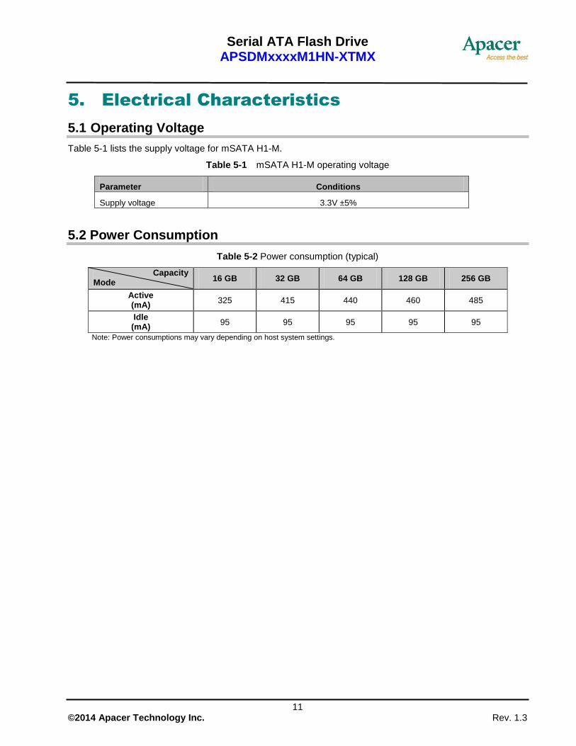
5.1 Operating Voltage
Table 5-1 lists the supply voltage for mSATA H1-M.
Table 5-1 mSATA H1-M operating voltage
Parameter Conditions
Supply voltage 3.3V ±5%
5.2 Power Consumption
Table 5-2 Power consumption (typical)
Capacity Mode
16 GB 32 GB 64 GB 128 GB 256 GB
Active (mA)
325 415 440 460 485
Idle (mA)
95 95 95 95 95
Note: Power consumptions may vary depending on host system settings.
Serial ATA Flash Drive APSDMxxxxM1HN-XTMX
12 © 2014 Apacer Technology Inc. Rev. 1.3
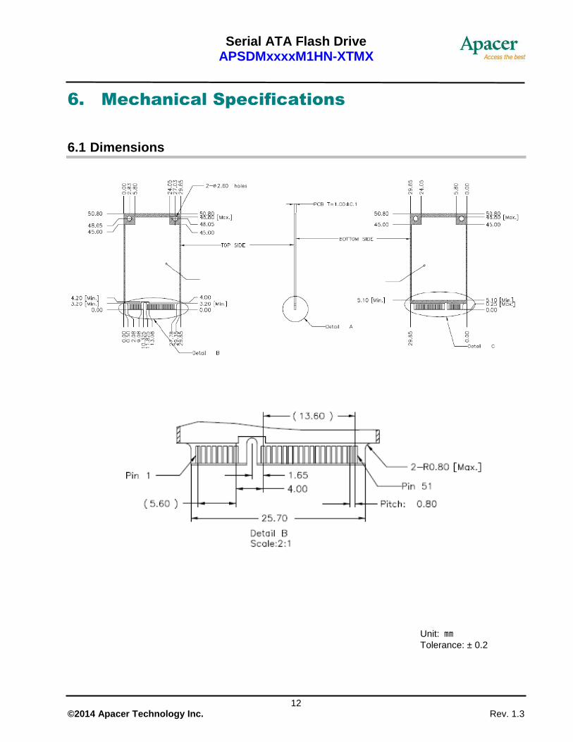
6. Mechanical Specifications
6.1 Dimensions
Unit: ㎜
Tolerance: ± 0.2
Serial ATA Flash Drive APSDMxxxxM1HN-XTMX
13 © 2014 Apacer Technology Inc. Rev. 1.3
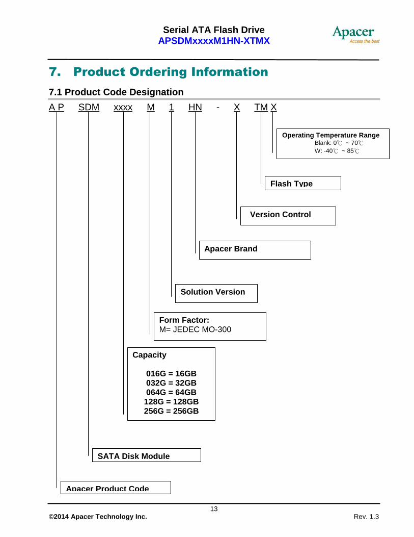
7. Product Ordering Information
7.1 Product Code Designation
A P SDM xxxx M 1 HN - X TM X
Apacer Brand
Solution Version
SATA Disk Module
Apacer Product Code
Capacity
016G = 16GB 032G = 32GB 064G = 64GB 128G = 128GB 256G = 256GB
Version Control
Flash Type
Form Factor: M= JEDEC MO-300
Operating Temperature Range Blank: 0℃ ~ 70℃
W: -40℃ ~ 85℃
Serial ATA Flash Drive APSDMxxxxM1HN-XTMX
14 © 2014 Apacer Technology Inc. Rev. 1.3
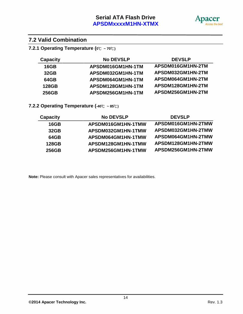
7.2 Valid Combination
7.2.1 Operating Temperature (0℃ ~ 70℃)
Capacity No DEVSLP DEVSLP
16GB APSDM016GM1HN-1TM APSDM016GM1HN-2TM
32GB APSDM032GM1HN-1TM APSDM032GM1HN-2TM
64GB APSDM064GM1HN-1TM APSDM064GM1HN-2TM
128GB APSDM128GM1HN-1TM APSDM128GM1HN-2TM
256GB APSDM256GM1HN-1TM APSDM256GM1HN-2TM
7.2.2 Operating Temperature (-40℃ ~ 85℃)
Capacity No DEVSLP DEVSLP
16GB APSDM016GM1HN-1TMW APSDM016GM1HN-2TMW
32GB APSDM032GM1HN-1TMW APSDM032GM1HN-2TMW
64GB APSDM064GM1HN-1TMW APSDM064GM1HN-2TMW
128GB APSDM128GM1HN-1TMW APSDM128GM1HN-2TMW
256GB APSDM256GM1HN-1TMW APSDM256GM1HN-2TMW
Note: Please consult with Apacer sales representatives for availabilities.
Serial ATA Flash Drive APSDMxxxxM1HN-XTMX
15 © 2014 Apacer Technology Inc. Rev. 1.3
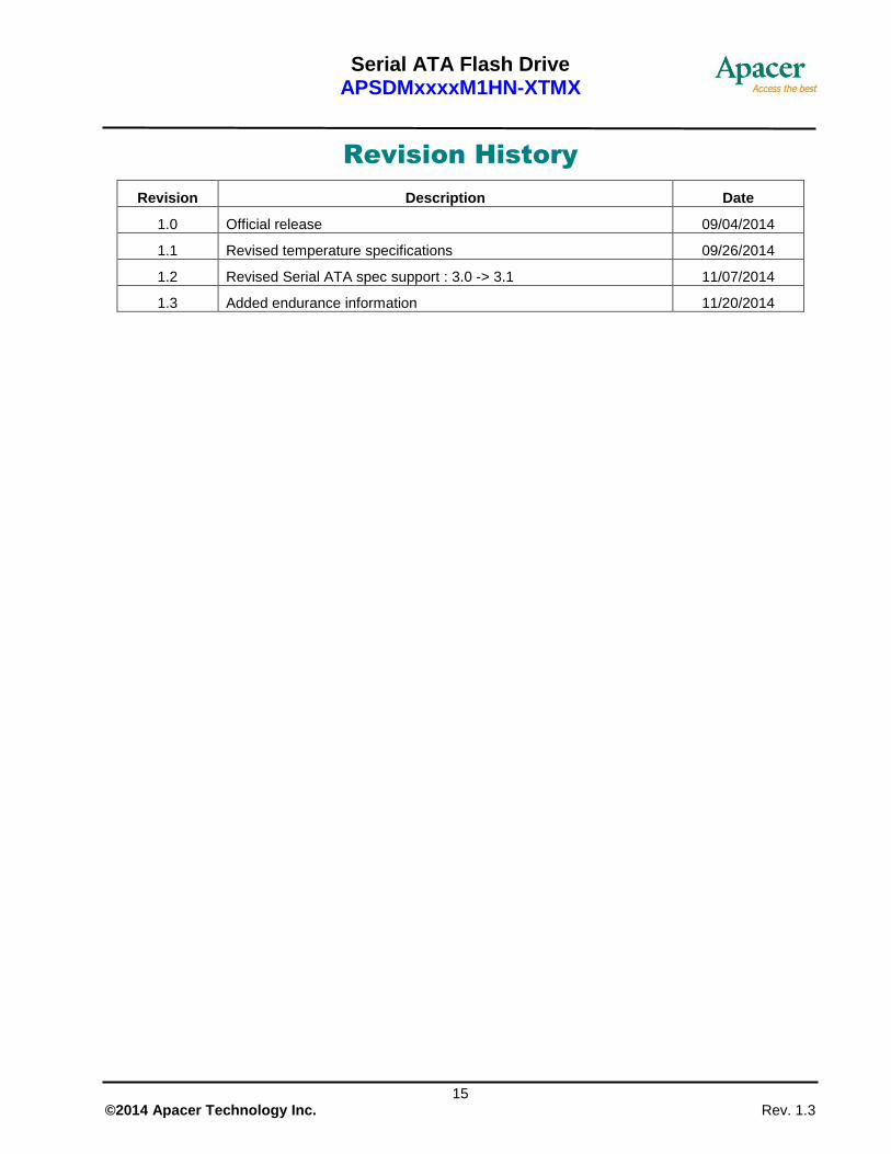
Revision History
Revision Description Date
1.0 Official release 09/04/2014
1.1 Revised temperature specifications 09/26/2014
1.2 Revised Serial ATA spec support : 3.0 -> 3.1 11/07/2014
1.3 Added endurance information 11/20/2014
Serial ATA Flash Drive APSDMxxxxM1HN-XTMX
16 © 2014 Apacer Technology Inc. Rev. 1.3
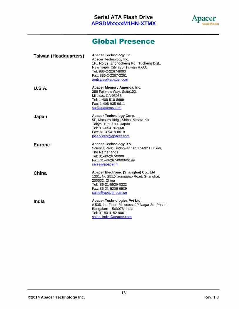
Global Presence
Taiwan (Headquarters)
Apacer Technology Inc.
Apacer Technology Inc. 1F., No.32, Zhongcheng Rd., Tucheng Dist., New Taipei City 236, Taiwan R.O.C. Tel: 886-2-2267-8000 Fax: 886-2-2267-2261 [email protected]
U.S.A.
Apacer Memory America, Inc.
386 Fairview Way, Suite102, Milpitas, CA 95035 Tel: 1-408-518-8699 Fax: 1-408-935-9611 [email protected]
Japan
Apacer Technology Corp.
5F, Matsura Bldg., Shiba, Minato-Ku Tokyo, 105-0014, Japan Tel: 81-3-5419-2668 Fax: 81-3-5419-0018 [email protected]
Europe
Apacer Technology B.V.
Science Park Eindhoven 5051 5692 EB Son, The Netherlands Tel: 31-40-267-0000 Fax: 31-40-267-0000#6199 [email protected]
China
Apacer Electronic (Shanghai) Co., Ltd
1301, No.251,Xiaomuqiao Road, Shanghai, 200032, China Tel: 86-21-5529-0222 Fax: 86-21-5206-6939 [email protected]
India
Apacer Technologies Pvt Ltd,
# 535, 1st Floor, 8th cross, JP Nagar 3rd Phase, Bangalore – 560078, India Tel: 91-80-4152-9061 [email protected]