Embed Size (px)
Citation preview
Embedded Systems SIETK
P a g e | 1
Unit 5 : Embedded communications protocols and Internet of things Synchronous/Asynchronous interfaces (like UART, SPI, I2C, USB), serial communication basics,
baud rate concepts, Interfacing digital and analog external device, Implementing and programming
UART, SPI and I2C, SPI interface using TM4C.Case Study: Tiva based embedded system
application using the interface protocols for communication with external devices “Sensor Hub
BoosterPack”. Embedded Networking fundamentals, IoT overview and architecture, Overview of
wireless sensor networks and design examples. Adding Wi-Fi capability to the Microcontroller,
Embedded Wi-Fi, User APIs for Wireless and Networking applications Building IoT applications
using CC3100 user API. Case Study: Tiva based Embedded Networking Application: “Smart Plug
with Remote disconnect and Wi-Fi connectivity.
Serial Communication basics:
Communication between electronic devices is like communication between humans. Both
sides need to speak the same language. In electronics, these languages are called communication
protocols. Luckily for us, there are only a few communication protocols (SPI,I2C,UART,USB) we
need to know when building most electronics projects.
SPI, I2C, and UART are quite a bit slower than protocols like USB, Ethernet, Bluetooth, and
Wi-Fi, but they’re a lot simpler and use less hardware and system resources. SPI, I2C, and UART are
ideal for communication between microcontrollers and between microcontrollers and sensors where
large amounts of high speed data don’t need to be transferred.
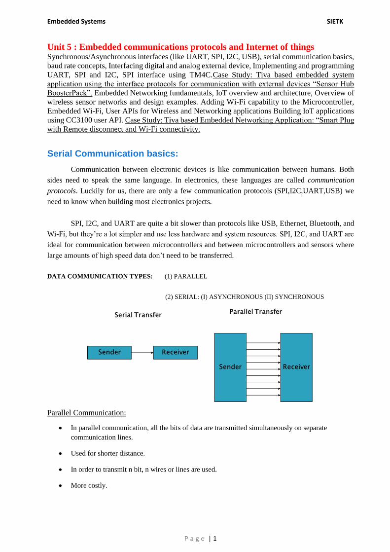
DATA COMMUNICATION TYPES: (1) PARALLEL
(2) SERIAL: (I) ASYNCHRONOUS (II) SYNCHRONOUS
Parallel Communication:
• In parallel communication, all the bits of data are transmitted simultaneously on separate
communication lines.
• Used for shorter distance.
• In order to transmit n bit, n wires or lines are used.
• More costly.
Embedded Systems SIETK
P a g e | 2
• Faster than serial transmission.
• Data can be transmitted in less time.
Example: printers and hard disk
Serial Communication:
• In serial communication the data bits are transmitted serially one by one i.e. bit by bit on single
communication line
• It requires only one communication line rather than n lines to transmit data from sender to
receiver.
• Thus all the bits of data are transmitted on single lines in serial fashion.
• Less costly.
• Long distance transmission.
Example: Telephone.
Serial communication uses two methods:
• Asynchronous.
• Synchronous.
Asynchronous:
• transfers single byte at a time • No need of clock signal
Example: UART (universal asynchronous receiver transmitter)
Synchronous:
• Transfers a block of data (characters) at a time. • Requires clock signal
Example: SPI (serial peripheral interface),
I2C (inter integrated circuit).
Embedded Systems SIETK
P a g e | 3
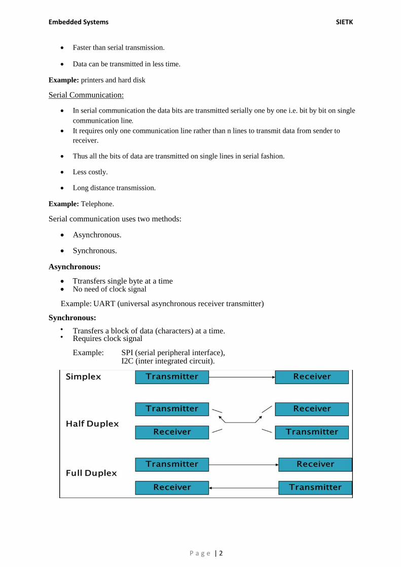
Data Transmission: In data transmission if the data can be transmitted and received, it is a
duplex transmission.
Simplex: Data is transmitted in only one direction i.e. from TX to RX only one TX and one RX
only
Half duplex: Data is transmitted in two directions but only one way at a time i.e. two TX's, two
RX’s and one line
Full duplex: Data is transmitted both ways at the same time i.e. two TX's, two RX’s and two
lines
A Protocol is a set of rules agreed by both the sender and receiver on
• How the data is packed
• How many bits constitute a character
• When the data begins and ends
Serial Synchronous Type Duplex
Data transfer
Protocol /Asynchronous rate (kbps)
UART Asynchronous peer-to-peer Full-duplex 20
I2C Synchronous multi-master Half-duplex 3400
SPI Synchronous multi-master Full-duplex >1,000
MICROWIRE Synchronous master/slave Full-duplex > 625
1-WIRE Asynchronous master/slave Half-duplex 16
Baud Rate Concepts:
Data transfer rate in serial communication is measured in terms of bits per second (bps).
This is also called as Baud Rate. Baud Rate and bps can be used inter changeably with respect to
UART.
Ex: The total number of bits gets transferred during 10 pages of text, each with 100 × 25
characters with 8 bits per character and 1 start & stop bit is:
For each character a total number of bits are 10. The total number of bits is: 100 × 25 ×
10 = 25,000 bits per page. For 10 pages of data it is required to transmit 2, 50,000 bits. Generally
Embedded Systems SIETK
P a g e | 4
baud rates of SCI are 1200, 2400, 4800, 9600, 19,200 etc. To transfer 2, 50,000 bits at a baud rate
of 9600, we need: 250000/9600 = 26.04 seconds (27 seconds).
Synchronous/Asynchronous Interfaces (like UART, SPI,
I2C, and USB):
Serial communication protocols can be categorized as Synchronous and Asynchronous
protocols. In synchronous communication, data is transmission and receiving is a continuous
stream at a constant rate. Synchronous communication requires the clock of transmitting device
and receiving device synchronized. In most of the systems, like ADC, audio codes,
potentiometers, transmission and reception of data occurs with same frequency. Examples of
synchronous communication are: I2C, SPI etc. In the case of asynchronous communication, the
transmission of data requires no clock signal and data transfer occurs intermittently rather than
steady stream. Handshake signals between the transmitter and receiver are important in
asynchronous communications. Examples of asynchronous communication are Universal
Asynchronous Receiver Transmitter (UART), USB, CAN etc.
Synchronous and asynchronous communication protocols are well-defined standards and
can be implemented in either hardware or software. In the early days of embedded systems,
Software implementation of I2C and SPI was common as well as a tedious work and used to take
long programs. Gradually, most the microcontrollers started incorporating the standard
communication protocols as hardware cores. This development in early 90‟s made job of the
embedded software development easy for communication protocols.
Microcontroller of our interest TM4C123 supports UART, CAN, SPI, I2C and USB
protocols. The five (UART, CAN, SPI, I2C and USB) above mentioned communication protocols
are available in most of the modern day microcontrollers. Before studying the implementation and
programming details of these protocols in TM4C123, it is required to understand basic standards,
features and applications.
UART COMMUNICATION PROTOCOL
In UART communication, two UARTs communicate directly with each other. The transmitting
UART converts parallel data from a controlling device like a CPU into serial form, transmits it in
serial to the receiving UART, which then converts the serial data back into parallel data for the
receiving device. Only two wires are needed to transmit data between two UARTs. Data flows
from the Tx pin of the transmitting UART to the Rx pin of the receiving UART:
UARTs transmit data asynchronously, which means there is no clock signal to synchronize the
output of bits from the transmitting UART to the sampling of bits by the receiving UART. Instead
of a clock signal, the transmitting UART adds start and stop bits to the data packet being
transferred. These bits define the beginning and end of the data packet so the receiving UART
knows when to start reading the bits.
Embedded Systems SIETK
P a g e | 5
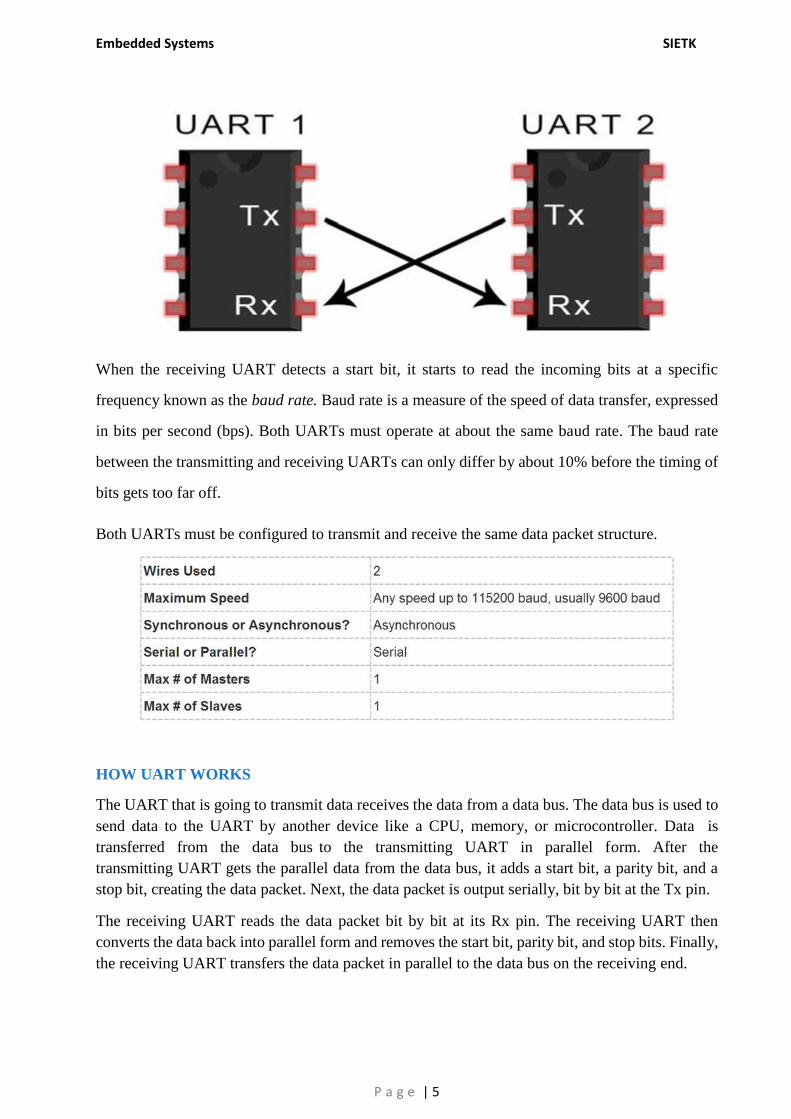
When the receiving UART detects a start bit, it starts to read the incoming bits at a specific
frequency known as the baud rate. Baud rate is a measure of the speed of data transfer, expressed
in bits per second (bps). Both UARTs must operate at about the same baud rate. The baud rate
between the transmitting and receiving UARTs can only differ by about 10% before the timing of
bits gets too far off.
Both UARTs must be configured to transmit and receive the same data packet structure.
HOW UART WORKS
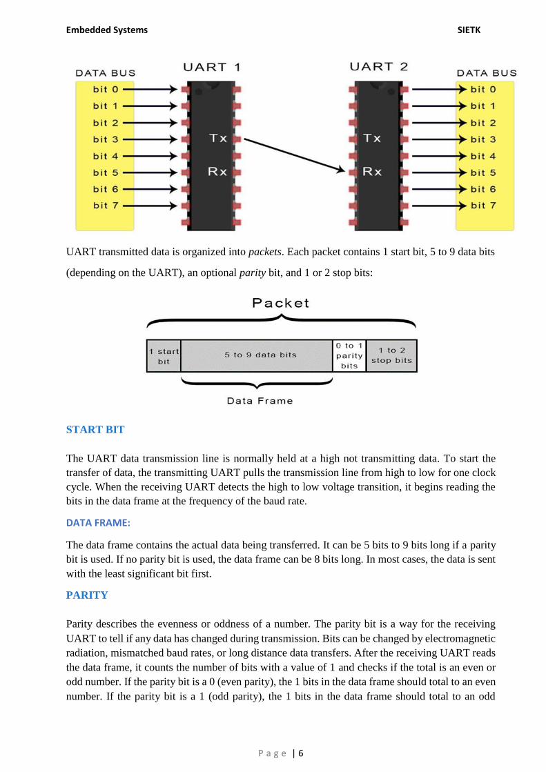
The UART that is going to transmit data receives the data from a data bus. The data bus is used to
send data to the UART by another device like a CPU, memory, or microcontroller. Data is
transferred from the data bus to the transmitting UART in parallel form. After the
transmitting UART gets the parallel data from the data bus, it adds a start bit, a parity bit, and a
stop bit, creating the data packet. Next, the data packet is output serially, bit by bit at the Tx pin.
The receiving UART reads the data packet bit by bit at its Rx pin. The receiving UART then
converts the data back into parallel form and removes the start bit, parity bit, and stop bits. Finally,
the receiving UART transfers the data packet in parallel to the data bus on the receiving end.
Embedded Systems SIETK
P a g e | 6
UART transmitted data is organized into packets. Each packet contains 1 start bit, 5 to 9 data bits
(depending on the UART), an optional parity bit, and 1 or 2 stop bits:
START BIT
The UART data transmission line is normally held at a high not transmitting data. To start the
transfer of data, the transmitting UART pulls the transmission line from high to low for one clock
cycle. When the receiving UART detects the high to low voltage transition, it begins reading the
bits in the data frame at the frequency of the baud rate.
DATA FRAME:
The data frame contains the actual data being transferred. It can be 5 bits to 9 bits long if a parity
bit is used. If no parity bit is used, the data frame can be 8 bits long. In most cases, the data is sent
with the least significant bit first.
PARITY
Parity describes the evenness or oddness of a number. The parity bit is a way for the receiving
UART to tell if any data has changed during transmission. Bits can be changed by electromagnetic
radiation, mismatched baud rates, or long distance data transfers. After the receiving UART reads
the data frame, it counts the number of bits with a value of 1 and checks if the total is an even or
odd number. If the parity bit is a 0 (even parity), the 1 bits in the data frame should total to an even
number. If the parity bit is a 1 (odd parity), the 1 bits in the data frame should total to an odd
Embedded Systems SIETK
P a g e | 7
number. When the parity bit matches the data, the UART knows that the transmission was free of
errors. But if the parity bit is a 0, and the total is odd; or the parity bit is a 1, and the total is even,
the UART knows that bits in the data frame have changed.
STOP BITS
The Stop Bit, as the name suggests, marks the end of the data packet. It is usually two bits long
but often only on bit is used. In order to end the transmission, the UART maintains the data line at
high voltage (1).
STEPS OF UART TRANSMISSION
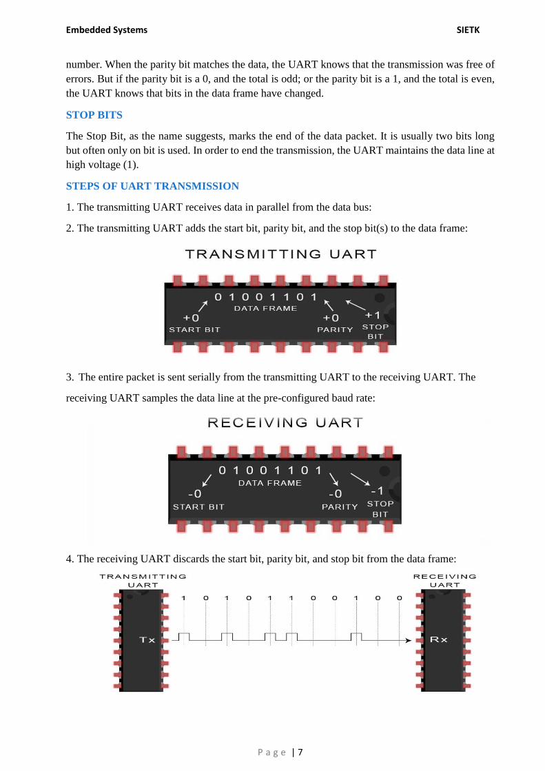
1. The transmitting UART receives data in parallel from the data bus:
2. The transmitting UART adds the start bit, parity bit, and the stop bit(s) to the data frame:
3. The entire packet is sent serially from the transmitting UART to the receiving UART. The
receiving UART samples the data line at the pre-configured baud rate:
4. The receiving UART discards the start bit, parity bit, and stop bit from the data frame:
Embedded Systems SIETK
P a g e | 8
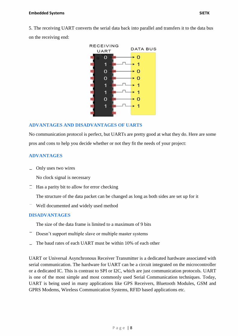
5. The receiving UART converts the serial data back into parallel and transfers it to the data bus
on the receiving end:
ADVANTAGES AND DISADVANTAGES OF UARTS
No communication protocol is perfect, but UARTs are pretty good at what they do. Here are some
pros and cons to help you decide whether or not they fit the needs of your project:
ADVANTAGES
Only uses two wires
No clock signal is necessary
Has a parity bit to allow for error checking
The structure of the data packet can be changed as long as both sides are set up for it
Well documented and widely used method
DISADVANTAGES
The size of the data frame is limited to a maximum of 9 bits
Doesn’t support multiple slave or multiple master systems
The baud rates of each UART must be within 10% of each other
UART or Universal Asynchronous Receiver Transmitter is a dedicated hardware associated with
serial communication. The hardware for UART can be a circuit integrated on the microcontroller
or a dedicated IC. This is contrast to SPI or I2C, which are just communication protocols. UART
is one of the most simple and most commonly used Serial Communication techniques. Today,
UART is being used in many applications like GPS Receivers, Bluetooth Modules, GSM and
GPRS Modems, Wireless Communication Systems, RFID based applications etc.
Embedded Systems SIETK
P a g e | 9
SPI COMMUNICATION PROTOCOL
SPI is a common communication protocol used by many different devices. For example, SD card
modules, RFID card reader modules, and 2.4 GHz wireless transmitter/receivers all use SPI to
communicate with microcontrollers.
One unique benefit of SPI is the fact that data can be transferred without interruption. Any
number of bits can be sent or received in a continuous stream. With I2C and UART, data is sent in
packets, limited to a specific number of bits. Start and stop conditions define the beginning and end
of each packet, so the data is interrupted during transmission.
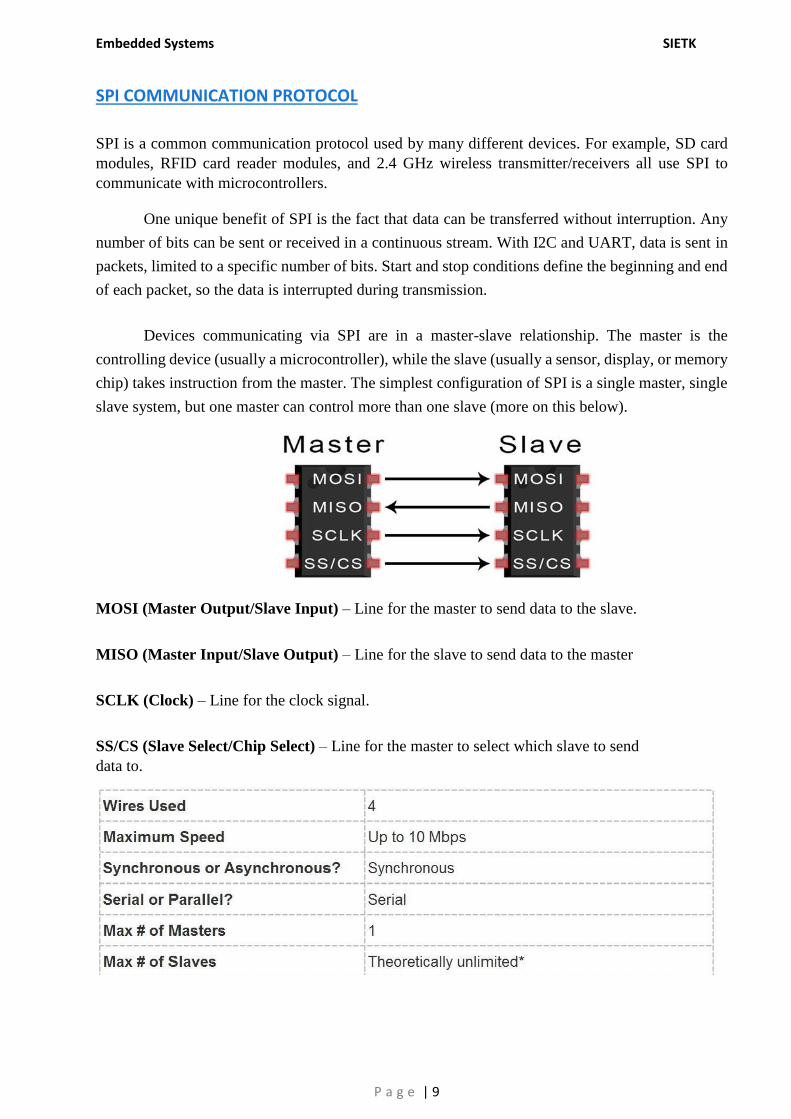
Devices communicating via SPI are in a master-slave relationship. The master is the
controlling device (usually a microcontroller), while the slave (usually a sensor, display, or memory
chip) takes instruction from the master. The simplest configuration of SPI is a single master, single
slave system, but one master can control more than one slave (more on this below).
MOSI (Master Output/Slave Input) – Line for the master to send data to the slave.
MISO (Master Input/Slave Output) – Line for the slave to send data to the master
SCLK (Clock) – Line for the clock signal.
SS/CS (Slave Select/Chip Select) – Line for the master to select which slave to send
data to.
Embedded Systems SIETK
P a g e | 10
*In practice, the number of slaves is limited by the load capacitance of the system, which reduces the
ability of the master to accurately switch between voltage levels.
HOW SPI WORKS
THE CLOCK
The clock signal synchronizes the output of data bits from the master to the sampling of bits by the
slave. One bit of data is transferred in each clock cycle, so the speed of data transfer is determined by
the frequency of the clock signal. SPI communication is always initiated by the master since the
master configures and generates the clock signal.
Any communication protocol where devices share a clock signal is known as synchronous. SPI is a
synchronous communication protocol. There are also asynchronous methods that don’t use a clock
signal. For example, on, in both sides are set to a pre-configured baud rate that dictates the speed and
timing of data transmission.
The clock signal in SPI can be modified using the properties of clock polarity and clock phase.
These two properties work together to define when the bits are output and when they are sampled.
Clock polarity can be set by the master to allow for bits to be output and sampled on either the rising
or falling edge of the clock cycle. Clock phase can be set for output and sampling to occur on either
the first edge or second edge of the clock cycle, regardless of whether it is rising or falling.
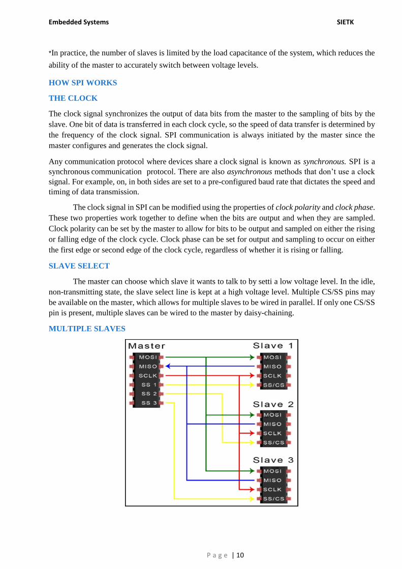
SLAVE SELECT
The master can choose which slave it wants to talk to by setti a low voltage level. In the idle,
non-transmitting state, the slave select line is kept at a high voltage level. Multiple CS/SS pins may
be available on the master, which allows for multiple slaves to be wired in parallel. If only one CS/SS
pin is present, multiple slaves can be wired to the master by daisy-chaining.
MULTIPLE SLAVES
Embedded Systems SIETK
P a g e | 11
SPI can be set up to operate with a single master and a single slave, and it can be set up with multiple
slaves controlled by a single master. There are two ways to connect multiple slaves to the master. If
the master has multiple slave select pins, the slaves can be wired in parallel like this:
If only one slave select pin is available, the slaves can be daisy-chained like this:
MOSI AND MISO
The master sends data to the slave bit by bit, in serial through the MOSI line. The slave
receives the data sent from the master at the MOSI pin. Data sent from the master to the slave is
usually sent with the most significant bit first.The slave can also send data back to the master through
the MISO line in serial. The data sent from the slave back to the master is usually sent with the least
significant bit first.
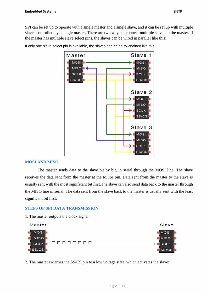
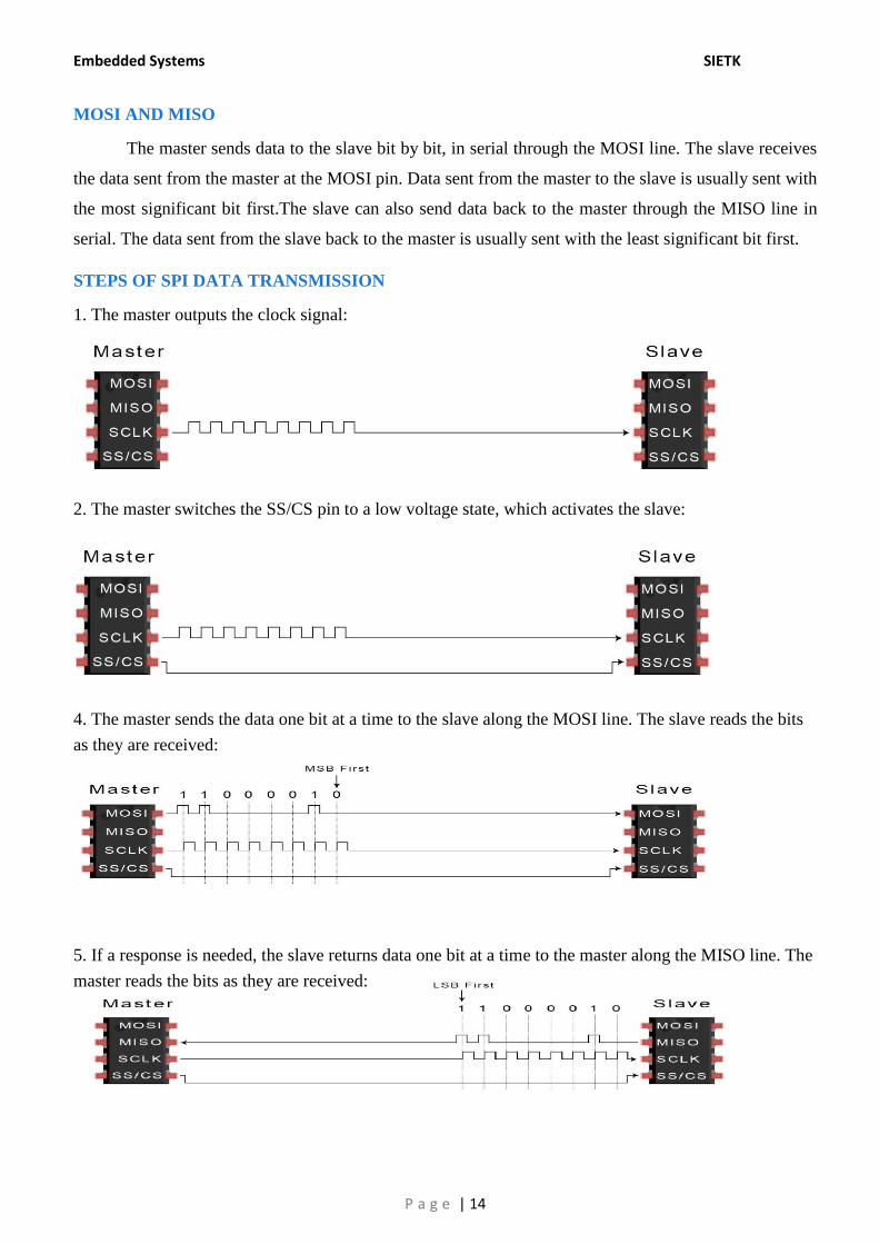
STEPS OF SPI DATA TRANSMISSION
1. The master outputs the clock signal:
2. The master switches the SS/CS pin to a low voltage state, which activates the slave:
Embedded Systems SIETK
P a g e | 12
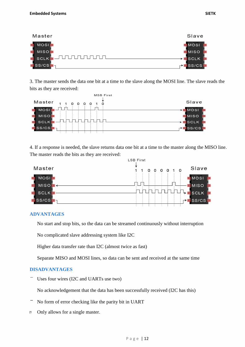
3. The master sends the data one bit at a time to the slave along the MOSI line. The slave reads the
bits as they are received:
4. If a response is needed, the slave returns data one bit at a time to the master along the MISO line.
The master reads the bits as they are received:
ADVANTAGES
No start and stop bits, so the data can be streamed continuously without interruption
No complicated slave addressing system like I2C
Higher data transfer rate than I2C (almost twice as fast)
Separate MISO and MOSI lines, so data can be sent and received at the same time
DISADVANTAGES
Uses four wires (I2C and UARTs use two)
No acknowledgement that the data has been successfully received (I2C has this)
No form of error checking like the parity bit in UART
Only allows for a single master.
Embedded Systems SIETK
P a g e | 13
I2C COMMUNICATION PROTOCOL
Inter IC (i2c) (IIC) is important serial communication protocol in modern electronic systems.
Philips invented this protocol in 1986. The objective of reducing the cost of production of television
remote control motivated Philips to invent this protocol. IIC is a serial bus interface, can be
implemented in software, but most of the microcontrollers support IIC by incorporating it as hard IP
(Intellectual Property). IIC can be used to interface microcontroller with RTC, EEPROM and
different variety of sensors. IIC is used to interface chips on motherboard, generally between a
processor chip and any peripheral which supports IIC. IIC is very reliable wireline communication
protocol for an on board or short distances. I2C is a serial protocol for two-wire interface to connect
low-speed devices like microcontrollers, EEPROMs, A/D and D/A converters, I/O interfaces and
other similar peripherals in embedded systems
I2C combines the best features of SPI and UARTs. With I2C, you can connect multiple slaves
to a single master (like SPI) and you can have multiple masters controlling single, or multiple slaves.
This is really useful when you want to have more than one microcontroller logging data to a single
memory card or displaying text to a single LCD.
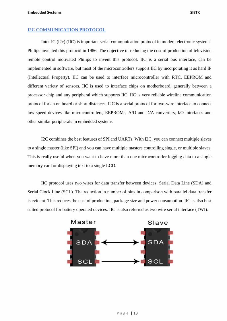
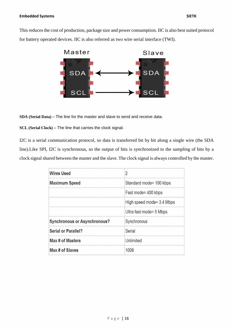
IIC protocol uses two wires for data transfer between devices: Serial Data Line (SDA) and
Serial Clock Line (SCL). The reduction in number of pins in comparison with parallel data transfer
is evident. This reduces the cost of production, package size and power consumption. IIC is also best
suited protocol for battery operated devices. IIC is also referred as two wire serial interface (TWI).
Embedded Systems SIETK
P a g e | 14
MOSI AND MISO
The master sends data to the slave bit by bit, in serial through the MOSI line. The slave receives
the data sent from the master at the MOSI pin. Data sent from the master to the slave is usually sent with
the most significant bit first.The slave can also send data back to the master through the MISO line in
serial. The data sent from the slave back to the master is usually sent with the least significant bit first.
STEPS OF SPI DATA TRANSMISSION
1. The master outputs the clock signal:
2. The master switches the SS/CS pin to a low voltage state, which activates the slave:
4. The master sends the data one bit at a time to the slave along the MOSI line. The slave reads the bits
as they are received:
5. If a response is needed, the slave returns data one bit at a time to the master along the MISO line. The
master reads the bits as they are received:
Embedded Systems SIETK
P a g e | 15
ADVANTAGES
No start and stop bits, so the data can be streamed continuously without interruption
No complicated slave addressing system like I2C
Higher data transfer rate than I2C (almost twice as fast)
Separate MISO and MOSI lines, so data can be sent and received at the same time
DISADVANTAGES
Uses four wires (I2C and UARTs use two)
No acknowledgement that the data has been successfully received (I2C has this)
No form of error checking like the parity bit in UART
Only allows for a single master.
I2C COMMUNICATION PROTOCOL
Inter IC (i2c) (IIC) is important serial communication protocol in modern electronic systems.
Philips invented this protocol in 1986. The objective of reducing the cost of production of television
remote control motivated Philips to invent this protocol. IIC is a serial bus interface, can be implemented
in software, but most of the microcontrollers support IIC by incorporating it as hard IP (Intellectual
Property). IIC can be used to interface microcontroller with RTC, EEPROM and different variety of
sensors. IIC is used to interface chips on motherboard, generally between a processor chip and any
peripheral which supports IIC. IIC is very reliable wireline communication protocol for an on board or
short distances. I2C is a serial protocol for two-wire interface to connect low-speed devices like
microcontrollers, EEPROMs, A/D and D/A converters, I/O interfaces and other similar peripherals in
embedded systems
I2C combines the best features of SPI and UARTs. With I2C, you can connect multiple slaves
to a single master (like SPI) and you can have multiple masters controlling single, or multiple slaves.
This is really useful when you want to have more than one microcontroller logging data to a single
memory card or displaying text to a single LCD.
IIC protocol uses two wires for data transfer between devices: Serial Data Line (SDA) and Serial
Clock Line (SCL). The reduction in number of pins in comparison with parallel data transfer is evident.
Embedded Systems SIETK
P a g e | 16
This reduces the cost of production, package size and power consumption. IIC is also best suited protocol
for battery operated devices. IIC is also referred as two wire serial interface (TWI).
SDA (Serial Data) – The line for the master and slave to send and receive data.
SCL (Serial Clock) – The line that carries the clock signal.
I2C is a serial communication protocol, so data is transferred bit by bit along a single wire (the SDA
line).Like SPI, I2C is synchronous, so the output of bits is synchronized to the sampling of bits by a
clock signal shared between the master and the slave. The clock signal is always controlled by the master.
Embedded Systems SIETK
P a g e | 17
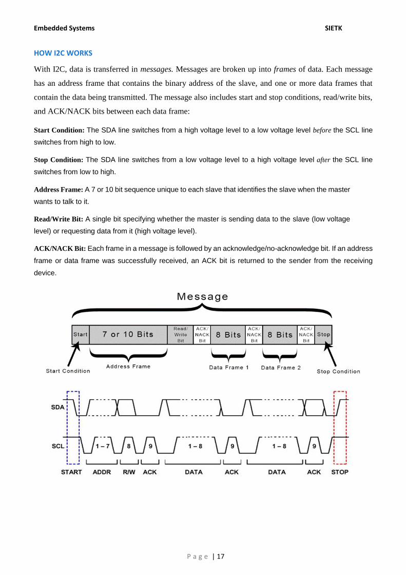
HOW I2C WORKS
With I2C, data is transferred in messages. Messages are broken up into frames of data. Each message
has an address frame that contains the binary address of the slave, and one or more data frames that
contain the data being transmitted. The message also includes start and stop conditions, read/write bits,
and ACK/NACK bits between each data frame:
Start Condition: The SDA line switches from a high voltage level to a low voltage level before the SCL line
switches from high to low.
Stop Condition: The SDA line switches from a low voltage level to a high voltage level after the SCL line
switches from low to high.
Address Frame: A 7 or 10 bit sequence unique to each slave that identifies the slave when the master
wants to talk to it.
Read/Write Bit: A single bit specifying whether the master is sending data to the slave (low voltage
level) or requesting data from it (high voltage level).
ACK/NACK Bit: Each frame in a message is followed by an acknowledge/no-acknowledge bit. If an address
frame or data frame was successfully received, an ACK bit is returned to the sender from the receiving
device.
Embedded Systems SIETK
P a g e | 18
ADDRESSING
I2C doesn’t have slave select it needs lines another like way to SPI let the slave so know that
data is being sent to it, and not another slave. It does this by addressing. The address frame is always the
first frame after the start bit in a new message.
The master sends the address of the slave it wants to communicate with to every slave connected
to it. Each slave then compares the address sent from the master to its own address. If the address
matches, it sends a low voltage ACK bit back to the match, the slave does nothing and the SDA line
remains high.
READ/WRITE BIT
The address frame includes a single bit at the end that informs the slave whether the master wants
to write data to it or receive data from it. If the master wants to send data to the slave, the read/write bit
is a low voltage level. If the master is requesting data from the slave, the bit is a high voltage level.
THE DATA FRAME
After the master detects the ACK bit from the slave, the first data frame is ready to be sent.
The data frame is always 8 bits long, and sent with the most significant bit first. Each data frame is
immediately followed by an ACK/NACK bit to verify that the frame has been received successfully.
The ACK bit must be received by either the master or the slave (depending on who is sending the data)
before the next data frame can be sent. After all of the data frames have been sent, the master can send
a stop condition to the slave to halt the transmission. The stop condition is a voltage transition from low
to high on the SDA line after a low to high transition on the SCL line, with the SCL line remaining high.
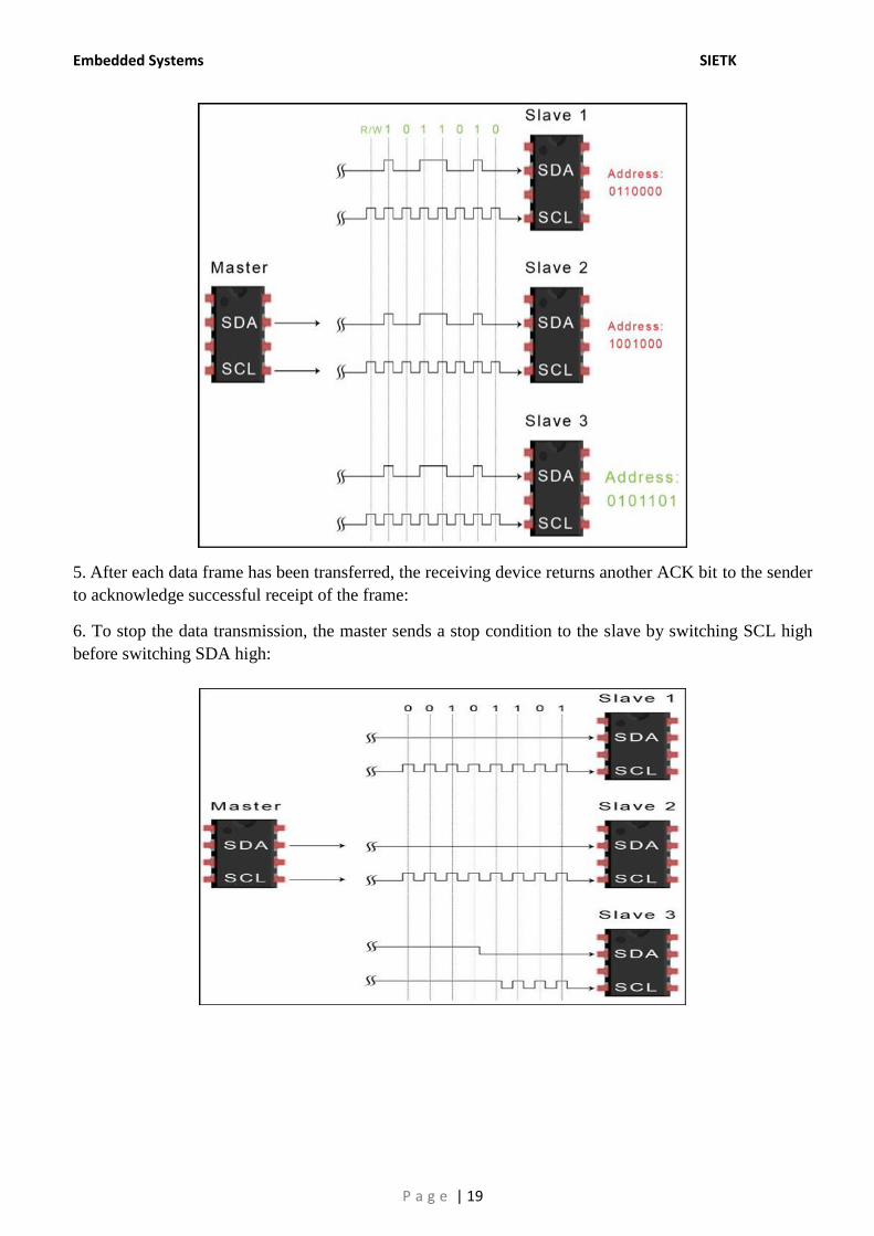
STEPS OF I2C DATA TRANSMISSION
1. The master sends the start condition to every connected slave by switching the SDA line from a high
voltage level to a low voltage level before switching the SCL line from high to low:
2. The master sends each slave the 7 or 10 bit address of the slave it wants to communicate with, along
with the read/write bit:
3. Each slave compares the address sent from the master to its own address. If the address
matches, the slave returns an ACK bit by pulling the SDA line low for one bit. If the address from
the master does not match the slave’s own address, SDA line high.
4. The master sends or receives the data frame:
Embedded Systems SIETK
P a g e | 19
5. After each data frame has been transferred, the receiving device returns another ACK bit to the sender
to acknowledge successful receipt of the frame:
6. To stop the data transmission, the master sends a stop condition to the slave by switching SCL high
before switching SDA high:
Embedded Systems SIETK
P a g e | 20
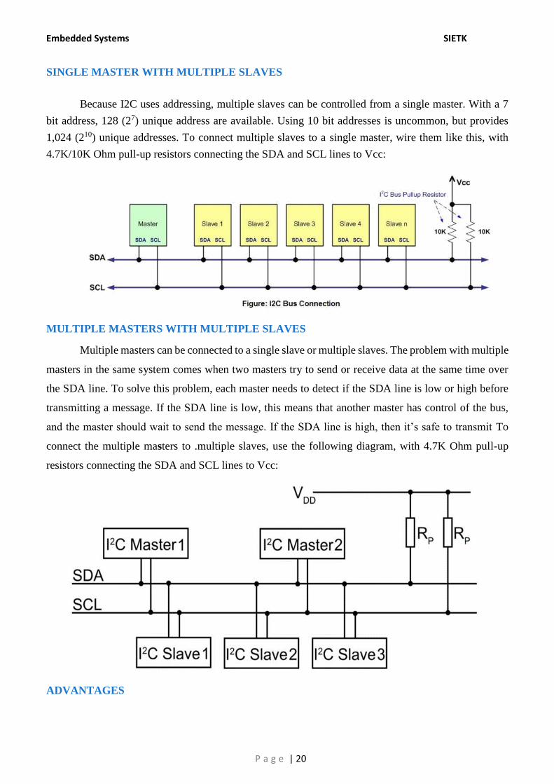
SINGLE MASTER WITH MULTIPLE SLAVES
Because I2C uses addressing, multiple slaves can be controlled from a single master. With a 7
bit address, 128 (27) unique address are available. Using 10 bit addresses is uncommon, but provides
1,024 (210) unique addresses. To connect multiple slaves to a single master, wire them like this, with
4.7K/10K Ohm pull-up resistors connecting the SDA and SCL lines to Vcc:
MULTIPLE MASTERS WITH MULTIPLE SLAVES
Multiple masters can be connected to a single slave or multiple slaves. The problem with multiple
masters in the same system comes when two masters try to send or receive data at the same time over
the SDA line. To solve this problem, each master needs to detect if the SDA line is low or high before
transmitting a message. If the SDA line is low, this means that another master has control of the bus,
and the master should wait to send the message. If the SDA line is high, then it’s safe to transmit To
connect the multiple masters to .multiple slaves, use the following diagram, with 4.7K Ohm pull-up
resistors connecting the SDA and SCL lines to Vcc:
ADVANTAGES
Embedded Systems SIETK
P a g e | 21
Only uses two wires
Supports multiple masters and multiple slaves
ACK/NACK bit gives confirmation that each frame is transferred successfully
Hardware is less complicated than with UARTs
Well known and widely used protocol
DISADVANTAGES
Slower data transfer rate than SPI
The size of the data frame is limited to 8 bits
More complicated hardware needed to implement than SPI
UNIVERSAL SERIAL BUS (USB)
Universal Serial Bus (USB) is a set of interface specifications for high speed wired communication
between electronics systems peripherals and devices with or without PC/computer. The USB was
originally developed in 1995 by many of the industry leading companies like Intel, Compaq, Microsoft,
Digital, IBM, and Northern Telecom.
The major goal of USB was to define an external expansion bus to add peripherals to a PC in easy and
simple manner. USB offers users simple connectivity. It eliminates the mix of different connectors for
different devices like printers, keyboards, mice, and other peripherals. That means USB-bus allows many
peripherals to be connected using a single standardized interface socket. It supports all kinds of data, from
slow mouse inputs to digitized audio and compressed video.
USB sends data in serial mode i.e. the parallel data is serialized before sends and de-serialized after
receiving. The benefits of USB are low cost, expandability, auto-configuration, hot-plugging and
outstanding performance. It also provides power to the bus, enabling many peripherals to operate without
the added need for an AC power adapter.
Embedded Systems SIETK
P a g e | 22
Various versions USB:
USB1.0: USB 1.0 is the original release of USB having the capability of transferring 12Mbps, supporting
up to 127 devices. This USB 1.0 specification model was introduced in January 1996.
USB1.1: USB 1.1 came out in September 1998. USB 1.1 is also known as full-speed USB. This version
is similar to the original release of USB; however, there are minor modifications for the hardware and the
specifications. USB version 1.1 supported two speeds, a full speed mode of 12Mbits/s and a low speed
mode of 1.5Mbits/s.
USB2.0: USB 2.0, also known as hi-speed USB. This hi-speed USB is capable of supporting a transfer
rate of up to 480 Mbps, compared to 12 Mbps of USB 1.1. That's about 40 times as fast! Wow!
USB3.0: It is also called as Super-Speed USB having a data transfer rate of 5Gbps. That means it can
deliver over 10x the speed of today's Hi-Speed USB connections.
USB3.1: It is also called as Super-Speed USB+ having a data transfer rate of 10Gbps.
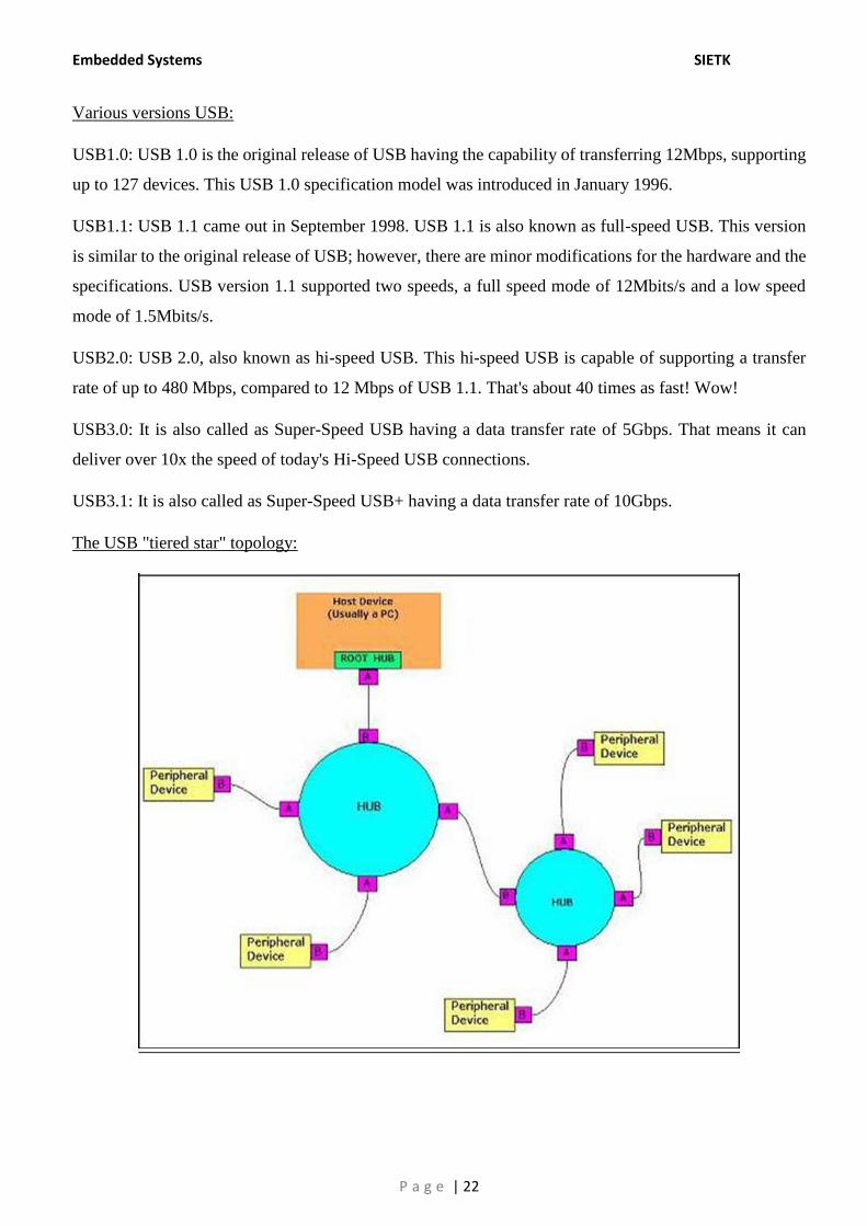
The USB "tiered star" topology:
Embedded Systems SIETK
P a g e | 23
The USB system is made up of a host, multiple numbers of USB ports, and multiple peripheral devices
connected in a tiered-star topology.
The host is the USB system's master, and as such, controls and schedules all communications activities.
Peripherals, the devices controlled by USB, are slaves responding to commands from the host. USB
devices are linked in series through hubs. There always exists one hub known as the root hub, which is
built in to the host controller.
By using different connectors on the upstream and downstream end, it is impossible to install a cable
incorrectly, because the two types are physically different.
Pin No Signal Color of the cable
1 +5V power Red
2 - Data White / Yellow
3 +Data Green / Blue
4 Ground Black/Brown
Table: USB pin connections
USB can support 4 data transfer types or transfer modes.
1. Control
2. Isochronous
3. Bulk
4. Interrupt
Control transfers exchange configuration, setup and command information between the device and host.
The host can also send commands or query parameters with control packets.
Isochronous transfer is used by time critical, streaming device such as speakers and video cameras. It is
time sensitive information so, within limitations, it has guaranteed access to the USB bus.
Bulk transfer is used by devices like printers & scanners, which receives data in one big packet.
Interrupt transfer is used by peripherals exchanging small amounts of data that need immediate attention.
Embedded Systems SIETK
P a g e | 24
All USB data is sent serially. USB data transfer is essentially in the form of packets of data, sent back
and forth between the host and peripheral devices. Initially all packets are sent from the host, via the root
hub and possibly more hubs, to devices.
Each USB data transfer consists of a…
1. Token packet (Header defining what it expects to follow)
2. Optional Data Packet (Containing the payload)
3. Status Packet (Used to acknowledge transactions and to provide a means of error correction).
Implementing and Programming UART:
TM4C123GH6PM microcontroller has got eight UART ports. They are named as UART0-UART7. In
the TI Launchpad, the UART0 port is connected to the ICDI (In-Circuit Debug Interface). ICDI is further
connected to USB port. Users can use UART0 for flash programming, debugging using JTAG. The UART
features of TI Tiva TM4C123GH6PM microcontroller is: -
• UART‟s have programmable baud-rate generator allowing speeds up to 5 Mbps for regular speed
and 10 Mbps for high speed.
• Separate 16x8 transmit (TX) and receive (RX) FIFOs to reduce CPU interrupt service loading with
programmable FIFO length
• Standard asynchronous communication bits for start, stop, and parity, Line-break generation and
detection
• Fully programmable serial interface characteristics o 5, 6, 7, or 8 data bits
• Even, odd, stick, or no-parity bit generation/detection o 1 or 2 stop bit generation
• IrDA serial-IR (SIR) encoder/decoder providing
• Programmable use of IrDA Serial Infrared (SIR) or UART input/output
• Support of IrDA SIR encoder/decoder functions for data rates up to 115.2 Kbps half duplex
• Support of normal 3/16 and low-power (1.41-2.23 μs) bit durations
• Programmable internal clock generator enabling division of reference clock by 1 to 256 for low-
power mode bit duration
• Support for communication with ISO 7816 smart cards
• Modem flow control (on UART1)
• EIA-485 9-bit support
• Standard FIFO-level and End-of-Transmission interrupts
Embedded Systems SIETK
P a g e | 25
• Efficient transfers using Micro Direct Memory Access Controller (μDMA) o Separate channels
for transmit and receive
• Receive single request asserted when data is in the FIFO; burst request asserted at programmed
FIFO level Transmit single request asserted when there is space in the FIFO; burst request asserted
at programmed FIFO level.
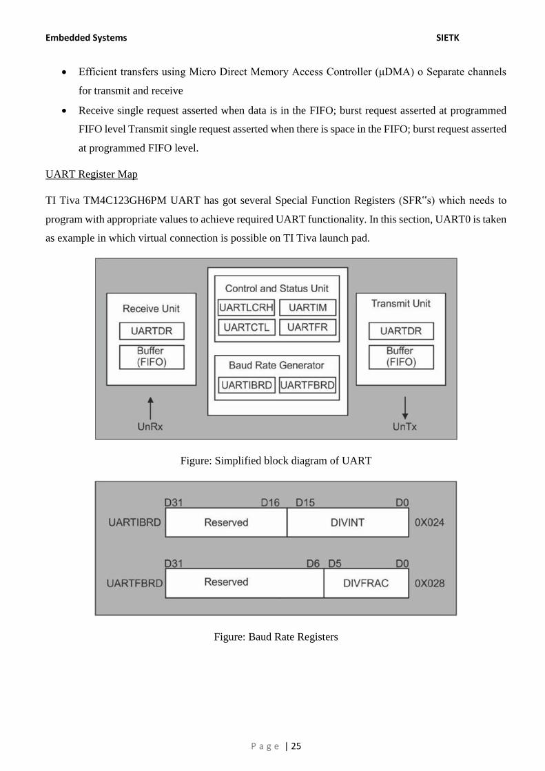
UART Register Map
TI Tiva TM4C123GH6PM UART has got several Special Function Registers (SFR‟s) which needs to
program with appropriate values to achieve required UART functionality. In this section, UART0 is taken
as example in which virtual connection is possible on TI Tiva launch pad.
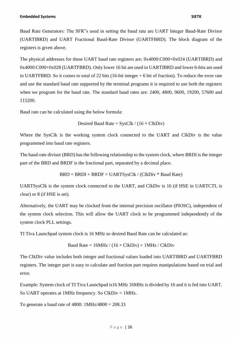
Figure: Simplified block diagram of UART
Figure: Baud Rate Registers
Embedded Systems SIETK
P a g e | 26
Baud Rate Generators: The SFR‟s used in setting the baud rate are UART Integer Baud-Rate Divisor
(UARTIBRD) and UART Fractional Baud-Rate Divisor (UARTFBRD). The block diagram of the
registers is given above.
The physical addresses for these UART baud rate registers are: 0x4000:C000+0x024 (UARTIBRD) and
0x4000:C000+0x028 (UARTFBRD). Only lower 16 bit are used in UARTIBRD and lower 6-bits are used
in UARTFBRD. So it comes to total of 22 bits (16-bit integer + 6 bit of fraction). To reduce the error rate
and use the standard baud rate supported by the terminal programs it is required to use both the registers
when we program for the baud rate. The standard baud rates are: 2400, 4800, 9600, 19200, 57600 and
115200.
Baud rate can be calculated using the below formula:
Desired Baud Rate = SysClk / (16 × ClkDiv)
Where the SysClk is the working system clock connected to the UART and ClkDiv is the value
programmed into baud rate registers.
The baud-rate divisor (BRD) has the following relationship to the system clock, where BRDI is the integer
part of the BRD and BRDF is the fractional part, separated by a decimal place.
BRD = BRDI + BRDF = UARTSysClk / (ClkDiv * Baud Rate)
UARTSysClk is the system clock connected to the UART, and ClkDiv is 16 (if HSE in UARTCTL is
clear) or 8 (if HSE is set).
Alternatively, the UART may be clocked from the internal precision oscillator (PIOSC), independent of
the system clock selection. This will allow the UART clock to be programmed independently of the
system clock PLL settings.
TI Tiva Launchpad system clock is 16 MHz so desired Baud Rate can be calculated as:
Baud Rate = 16MHz / (16 × ClkDiv) = 1MHz / ClkDiv
The ClkDiv value includes both integer and fractional values loaded into UARTIBRD and UARTFBRD
registers. The integer part is easy to calculate and fraction part requires manipulations based on trial and
error.
Example: System clock of TI Tiva Launchpad is16 MHz 16MHz is divided by 16 and it is fed into UART.
So UART operates at 1MHz frequency. So ClkDiv = 1MHz.
To generate a baud rate of 4800: 1MHz/4800 = 208.33
Embedded Systems SIETK
P a g e | 27
(a) 1MHz/4800 = 208.33, UARTIBRD=208 & UARTFBRD = (0.33×64) + 0.5 = 21.83 =21
(b) 1MHz/9600 = 104.166666, UARTIBRD = 104 & UARTFBRD = (0.16666×64) +0.5=11
(c) 1MHz/57600 = 17.361, UARTIBRD = 17 and UARTFBRD = (0.361 × 64) + 0.5 =23
(d) 1MHz/115200 = 8.680, UARTIBRD = 8 and UARTFBRD = (0.680 × 64) +0.5=44
Serial IR (SIR):
UART includes an IrDA (Infrared) serial IR encoder-decoder block. SIR block converts the data between
UART and half-duplex serial SIR interface. The SIR block provides a digitally encoded output and
decoded input to UART. SIR block uses UnTx and UnRx pins for SIR interface. These pins are connected
to IrDA SIR physical layer link. SIR block supports half-duplex communication. The IrDA SIR physical
layer specifies a minimum 10-ms delay between transmission and reception. The SIR block has two modes
of operation normal mode and low power mode.
ISO 7816 Support: UART support ISO 7816 smartcard communication. The UnTx signal is used as a bit
clock and the UnRx signal is used as the half-duplex communication line connected to the smartcard. Any
GPIO signal can be used to generate the reset signal to the smartcard.
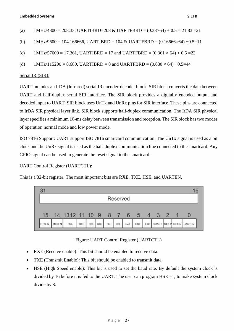
UART Control Register (UARTCTL):
This is a 32-bit register. The most important bits are RXE, TXE, HSE, and UARTEN.
Figure: UART Control Register (UARTCTL)
• RXE (Receive enable): This bit should be enabled to receive data.
• TXE (Transmit Enable): This bit should be enabled to transmit data.
• HSE (High Speed enable): This bit is used to set the baud rate. By default the system clock is
divided by 16 before it is fed to the UART. The user can program HSE =1, to make system clock
divide by 8.
Embedded Systems SIETK
P a g e | 28
• UARTEN (UART enable): This bit allows user to enable or disable the UART. During the
initialization of the UART registers, this is disabled. To disable UART under any circumstances,
this bit is used.
• SIREN (SIR Enable): IrDA SIR Block is enabled. UART will transmit and receive data using SIR
protocol.
• SIRLP (SIR Low Power Mode): This bit selects the IrDA encoding mode: Normal mode or low
power mode.
• SMART (ISO 7816 Smart Card support): The UART operates in Smart Card mode when SMART
= 1. UART does not support automatic retransmission on parity errors. If a parity error is detected
on transmission, all further transmit operations are aborted and software must handle
retransmission of the affected byte or message.
• LBE (Loop Back Enable): The UnTx path is fed through the UnRx path when LBE =1.
• RTSEN (Enable Request to send): RTS hardware flow control is enabled. Data is only requested
when receive FIFO has available entries.
• RTS (Request to send): When RTSEN is clear, the status of this bit is reflected on the U1RTS
signal. If RTSEN is set, this bit is ignored on a write and should be ignored on read.
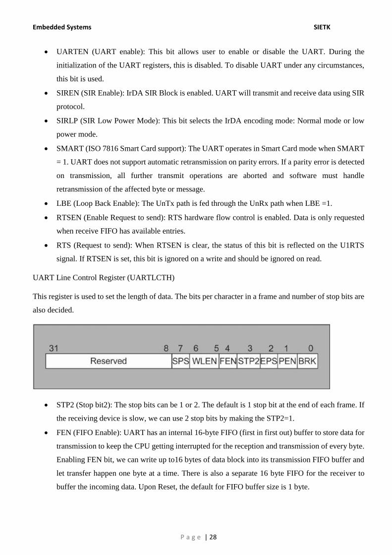
UART Line Control Register (UARTLCTH)
This register is used to set the length of data. The bits per character in a frame and number of stop bits are
also decided.
• STP2 (Stop bit2): The stop bits can be 1 or 2. The default is 1 stop bit at the end of each frame. If
the receiving device is slow, we can use 2 stop bits by making the STP2=1.
• FEN (FIFO Enable): UART has an internal 16-byte FIFO (first in first out) buffer to store data for
transmission to keep the CPU getting interrupted for the reception and transmission of every byte.
Enabling FEN bit, we can write up to16 bytes of data block into its transmission FIFO buffer and
let transfer happen one byte at a time. There is also a separate 16 byte FIFO for the receiver to
buffer the incoming data. Upon Reset, the default for FIFO buffer size is 1 byte.
Embedded Systems SIETK
P a g e | 29
• WLEN (Word Length): The number of bits per character data in each frame can be 5, 6, 7, or 8.
we use 8 bits for each character data frame. Default world length mode is 5.
• BRK (Send Break): A Low level is continually output on the UnTx signal, after completing
transmission of the current character. For the proper execution of the break command, software
must set this bit for at least two frames (character periods).
• PEN (Parity Enable): Parity is enabled and parity bit is added to the data frame by making PEN =
1. Parity checking is also enabled.
• EPS (Even Parity Select): Odd parity is performed, which checks for an odd number of 1s when
EPS = 0. Even parity generation and checking is performed during transmission and reception,
which checks for an even number of 1s in data and parity bits when EPS = 1.
UART Data Register (UARTDR):
Figure: UART Date Register (UARTDR)
Data should be placed in data register before transmission. Only lower 8 bits are used. In a similar way,
the received byte should be read and saved in memory before it gets overwrite by next byte. During
reception, we use other four bits (8, 9, 10 and 11) to detect error, parity etc. Another set of registers are
used to check the source of error. (UARTRSR/UARTRCR)
• OE: Overrun error (OE = 0: No data is lost).
• BE: Break error
• PE: Parity error
• FE: Framing error.
UART Flag Register (UARTFR):
The UART Flag Register holds one byte of data when FIFO buffer is disabled.
Embedded Systems SIETK
P a g e | 30
Figure: UART Flag Register (UARTFR)
• TXFE (TX FIFO Empty): Transmitter loads one byte for transmission from the FIFO buffer.
• When FIFO becomes empty, the TXFE is raised. The transmitter then frames the byte and sends
it out via TxD pin bit by bit serially.
• RXFF (RX FIFO Full): When a byte of data is received, byte is placed in Data register and RXFF
(RX FIFO full) flag bit is raised after receiving the complete byte.
• TXFF (TX FIFOI Full): When the transmitter is not busy, it loads one byte from the FIFO buffer
and the FIFO is not full anymore and the TXFF is lowered. We can monitor TXFF flag and upon
going LOW we can write another byte to the Data register.
UART Transmission
Step to perform UART Transmission:
• Program the RCGCUART register to get clock on UART0.
• Program the RCGCGPIO register to get the clock for PORTA.
• Program UARTCTL to disable UART0.
• Program the integer part and fractional part into baud rate registers: UARTIBRD and UARTFBRD
for UART0.
• Program UARTCC to select the system clock as UART clock.
• Set the bits in UARTLCRH register for 1 stop bit, no interrupt, no FIFO use, and for 8-bit date
size (for UART 0).
• Program TxE and RxE in UARTCTL to enable transmitter and receiver.
• Make PA0 and PA1 pins to use as digital pins.
• Configure PA0 and PA1 pins for UART.
Embedded Systems SIETK
P a g e | 31
• Loop the program for wait on TxD output. Monitor the TXFF flag bit and when it goes low, write
a data into data register.
UART Reception
Step by Step Execution of UART Reception:
• Program the RCGCUART register to get clock on UART0.
• Program the RCGCGPIO register to get the clock for PORTA.
• Program UARTCTL to disable UART0.
• Program the integer part and fractional part into baud rate registers: UARTIBRD and UARTFBRD
for UART0.
• Program UARTCC to select the system clock as UART clock.
• Set the bits in UARTLCRH register for 1 stop bit, no interrupt, no FIFO use, and for 8 -bit data
size (for UART 0).
• Program TxE and RxE in UARTCTL to enable transmitter and receiver.
• Make PA0 and PA1 pins to use as digital pins.
• Configure PA0 and PA1 pins for UART.
• Loop the program for wait on TxD output. Monitor the TXFF flag bit and when it goes low, write
a data into data register.
• Monitor the RXFE flag bit in UART Flag register and when it goes LOW read the received byte
from Data register and save before it gets overwrite.
Basic UART programing
Example 1:
Program to send the characters "HELLO" to HyperTerminal of PC
#include <stdint.h>
#include "tm4c123gh6pm.h"
void UART0Tx(char c);
void delayMs(int n);
int main(void)
SYSCTL->RCGCUART |= 1; /* enable clock supply to UART*/
Embedded Systems SIETK
P a g e | 32
SYSCTL->RCGCGPIO |= 1; /* enable clock supply to PORTA */ /* UART0 initialization */
UART0->CTL = 0; /* disable UART0 */
UART0->IBRD = 104; /* 9600 baud rate
UART0->FBRD = 11; /* fractional portion*/
UART0->CC = 0; /* configured to system clock */
UART0->LCRH = 0x60; /* 8-bit, no parity, 1-stop bit, no FIFO */ UART0->CTL = 0x301; /* configure
UART0 and TXE, RXE*/ /* UART0 TX0 and RX0 use PA0 and PA1. Set them up. */ GPIOA->DEN =
0x03; /* Make PA0 and PA1 as digital */
GPIOA->AFSEL = 0x03; /* Use PA0, PA1 alternate function */ GPIOA->PCTL = 0x11; /* configure
PA0 and PA1 for UART */ delayMs(1); /* wait for output line to stabilize */
for(;;)
{
UART0Tx('H');
UART0Tx('E');
UART0Tx('L');
UART0Tx('L ');
UART0Tx('O');
}
}
/* UART0 Transmit */ /* wait until Tx buffer not full */
void UART0Tx(char c) /* before giving it another byte */
{
while((UART0->FR & 0x20) != 0);
UART0->DR = c;
}
Example 2:
Program to receive data serially via UART0
#include <stdint.h>
#include "tm4c123gh6pm.h"
char UART0Rx(void);
void delayMs(int n);
Embedded Systems SIETK
P a g e | 33
int main(void)
{
char c;
SYSCTL->RCGCUART |= 1; /* enable clock supply to UART*/
SYSCTL->RCGCGPIO |= 1; /* enable clock supply to PORTA */
/* UART0 initialization */
UART0->CTL = 0; /* disable UART0 */
UART0->IBRD = 104; /* 9600 baud rate */
UART0->FBRD = 11; /* fractional portion*/
UART0->CC = 0; /* configured to system clock */
UART0->LCRH = 0x60; /* 8-bit, no parity, 1-stop bit, no FIFO */
UART0->CTL = 0x301; /* configure UART0 and TXE, RXE */
/* UART0 TX0 and RX0 use PA0 and PA1. Set them up. */
GPIOA->DEN = 0x03; /* Make PA0 and PA1 as digital */
GPIOA->AFSEL = 0x03; /* Use PA0, PA1 alternate function */
GPIOA->PCTL = 0x11; /* configure PA0 and PA1 for UART */
for(;;)
{
c = UART0Rx(); /* get a character from UART */
}
}
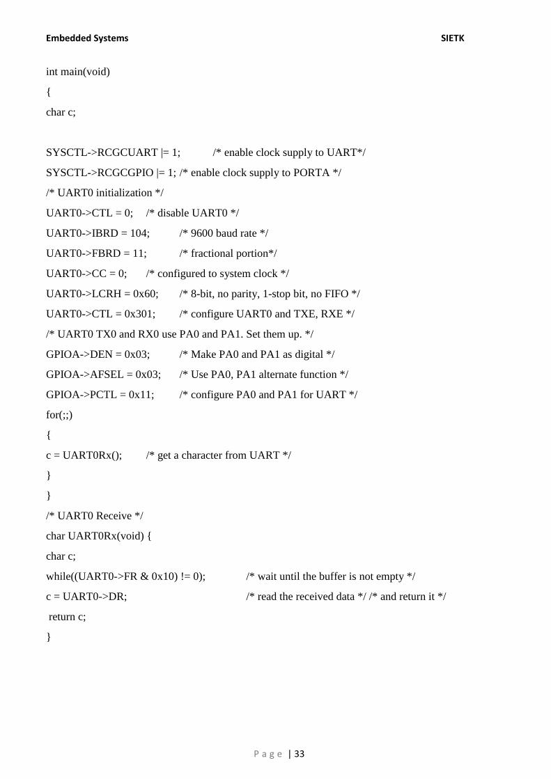
/* UART0 Receive */
char UART0Rx(void) {
char c;
while((UART0->FR & 0x10) != 0); /* wait until the buffer is not empty */
c = UART0->DR; /* read the received data */ /* and return it */
return c;
}
Embedded Systems SIETK
P a g e | 34
Implementing and Programming I2C:
• The TM4C123GH6PM controller includes four I2C modules with the following features:
• Devices on the I2C bus can be designated as either a master or a slave
• Supports both transmitting and receiving data as either a master or a slave
• Supports simultaneous master and slave operation
• Four I2C modes
o Master transmit o Master receive o Slave transmit o Slave receive
• Four transmission speeds: o Standard (100 Kbps) o Fast-mode (400 Kbps)
o Fast-mode plus (1 Mbps) o High-speed mode (3.33 Mbps)
• Clock low timeout interrupt
• Dual slave address capability
• Glitch suppression
• Master and slave interrupt generation
• Master generates interrupts when a transmit or receive operation completes (or aborts due to an
error)
• Slave generates interrupts when data has been transferred or requested by a master or when a
START or STOP condition is detected
• Master with arbitration and clock synchronization, multi-master support, and 7-bit addressing
mode.
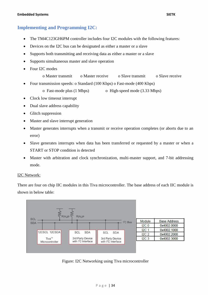
I2C Network:
There are four on chip IIC modules in this Tiva microcontroller. The base address of each IIC module is
shown in below table:
Figure: I2C Networking using Tiva microcontroller
Embedded Systems SIETK
P a g e | 35
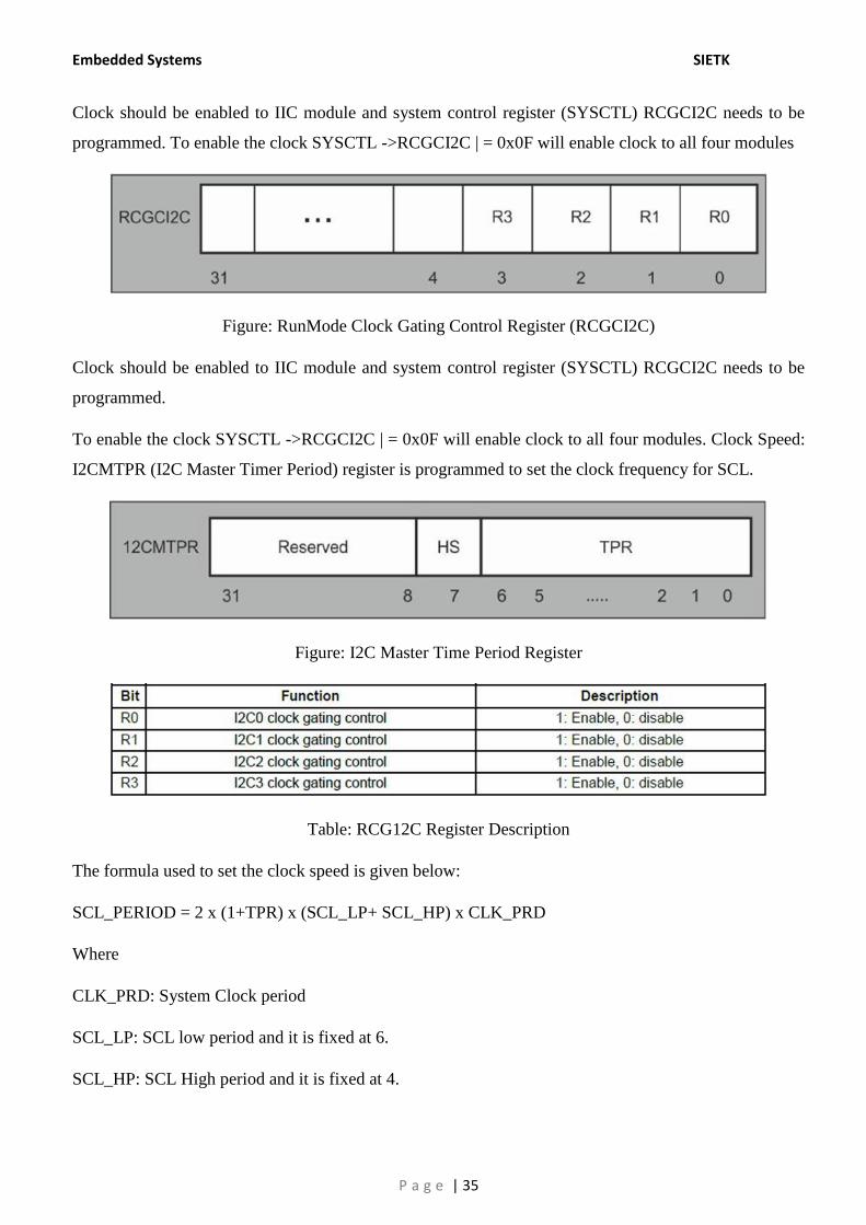
Clock should be enabled to IIC module and system control register (SYSCTL) RCGCI2C needs to be
programmed. To enable the clock SYSCTL ->RCGCI2C | = 0x0F will enable clock to all four modules
Figure: RunMode Clock Gating Control Register (RCGCI2C)
Clock should be enabled to IIC module and system control register (SYSCTL) RCGCI2C needs to be
programmed.
To enable the clock SYSCTL ->RCGCI2C | = 0x0F will enable clock to all four modules. Clock Speed:
I2CMTPR (I2C Master Timer Period) register is programmed to set the clock frequency for SCL.
Figure: I2C Master Time Period Register
Table: RCG12C Register Description
The formula used to set the clock speed is given below:
SCL_PERIOD = 2 x (1+TPR) x (SCL_LP+ SCL_HP) x CLK_PRD
Where
CLK_PRD: System Clock period
SCL_LP: SCL low period and it is fixed at 6.
SCL_HP: SCL High period and it is fixed at 4.
Embedded Systems SIETK
P a g e | 36
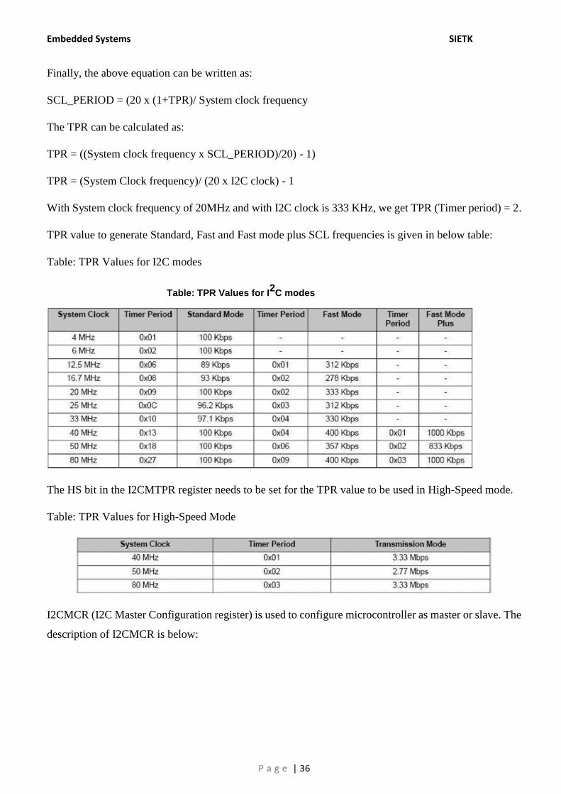
Finally, the above equation can be written as:
SCL_PERIOD = (20 x (1+TPR)/ System clock frequency
The TPR can be calculated as:
TPR = ((System clock frequency x SCL_PERIOD)/20) - 1)
TPR = (System Clock frequency)/ (20 x I2C clock) - 1
With System clock frequency of 20MHz and with I2C clock is 333 KHz, we get TPR (Timer period) = 2.
TPR value to generate Standard, Fast and Fast mode plus SCL frequencies is given in below table:
Table: TPR Values for I2C modes
The HS bit in the I2CMTPR register needs to be set for the TPR value to be used in High-Speed mode.
Table: TPR Values for High-Speed Mode
I2CMCR (I2C Master Configuration register) is used to configure microcontroller as master or slave. The
description of I2CMCR is below:
Table: TPR Values for I2
C modes
Embedded Systems SIETK
P a g e | 37
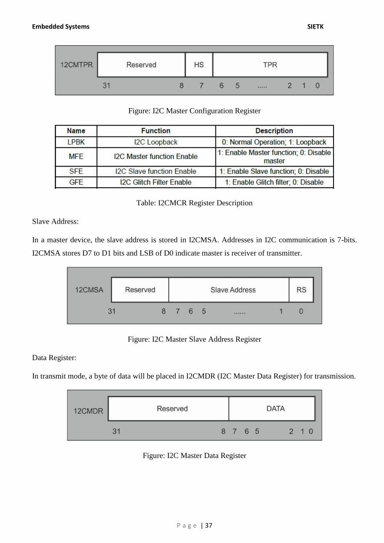
Figure: I2C Master Configuration Register
Table: I2CMCR Register Description
Slave Address:
In a master device, the slave address is stored in I2CMSA. Addresses in I2C communication is 7-bits.
I2CMSA stores D7 to D1 bits and LSB of D0 indicate master is receiver of transmitter.
Figure: I2C Master Slave Address Register
Data Register:
In transmit mode, a byte of data will be placed in I2CMDR (I2C Master Data Register) for transmission.
Figure: I2C Master Data Register

Embedded Systems SIETK
P a g e | 38
Control and Status Flag Register:
The I2CMCS (I2C Master Control/Status) register is programmed for both control and status. I2CMCS
register configures the I2C controller operation. The status whether a byte has been transmitted. That is,
transmission buffer is empty and ready to transmit the next byte. After writing a data into I2C Data register
and the slave address into I2C Master Slave address register, we can configure I2CMCS register for the
I2C to start a data transmission from Master to slave device. Writing 0x07 to I2CMCS register has all the
three of STOP = 1, RUN = 1, and START = 1 in it. To check the status of transmission, we poll the
BUSBSY bit of I2CMCS register. BUSBSY bit goes low after transmission complete. Program should
also check the ERROR bit to confirm that no error has occurred during transmission. For any error in
transmission, detected by transmitter or raised by slave, the ADRACK and DATACK will be set. The bit
ARBLST should be polled, to confirm transmitter has got access to bus and not lost arbitration.
Figure: I2C Master Control/Status Register
Table: I2C MCS Register Description
Embedded Systems SIETK
P a g e | 39
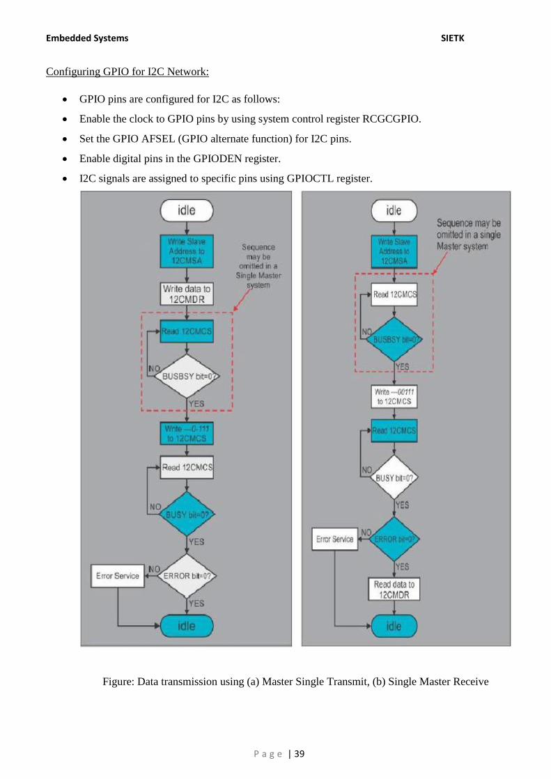
Configuring GPIO for I2C Network:
• GPIO pins are configured for I2C as follows:
• Enable the clock to GPIO pins by using system control register RCGCGPIO.
• Set the GPIO AFSEL (GPIO alternate function) for I2C pins.
• Enable digital pins in the GPIODEN register.
• I2C signals are assigned to specific pins using GPIOCTL register.
Figure: Data transmission using (a) Master Single Transmit, (b) Single Master Receive
Embedded Systems SIETK
P a g e | 40
Implementing and Programming SPI:
Serial peripheral interface (SPI) is a serial communication interface originally designed by Motorola in
late eighties. SPI and I2C came into existence almost at the same time. Most of the modern day
microcontrollers will support SPI protocol. Both SPI and I2C offer good support for communication
with low-speed devices, but SPI is better suited to applications in which devices transfer data streams.
Some devices use the full-duplex mode to implement an efficient, swift data stream for applications such
as digital audio, digital signal processing, or telecommunications channels, but most off-the-shelf chips
stick to half-duplex request/response protocols.
SPI is used to talk to a variety of peripherals, such a
• Sensors: temperature, pressure, ADC, touchscreens, video game controllers
• Control devices: audio codecs, digital potentiometers, DAC
• Camera lenses: Canon EF lens mount
• Memory: flash and EEPROM
• Real-time clocks
• LCD, sometimes even for managing image data
• Any MMC or SD card
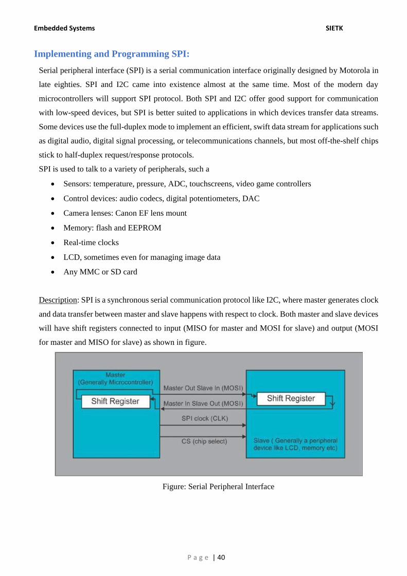
Description: SPI is a synchronous serial communication protocol like I2C, where master generates clock
and data transfer between master and slave happens with respect to clock. Both master and slave devices
will have shift registers connected to input (MISO for master and MOSI for slave) and output (MOSI
for master and MISO for slave) as shown in figure.
Figure: Serial Peripheral Interface
Embedded Systems SIETK
P a g e | 41
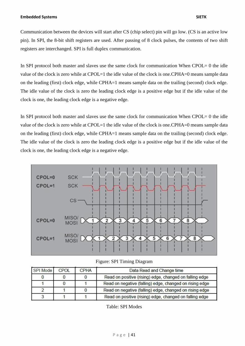
Communication between the devices will start after CS (chip select) pin will go low. (CS is an active low
pin). In SPI, the 8-bit shift registers are used. After passing of 8 clock pulses, the contents of two shift
registers are interchanged. SPI is full duplex communication.
In SPI protocol both master and slaves use the same clock for communication When CPOL= 0 the idle
value of the clock is zero while at CPOL=1 the idle value of the clock is one.CPHA=0 means sample data
on the leading (first) clock edge, while CPHA=1 means sample data on the trailing (second) clock edge.
The idle value of the clock is zero the leading clock edge is a positive edge but if the idle value of the
clock is one, the leading clock edge is a negative edge.
Figure: SPI Timing Diagram
Table: SPI Modes
Embedded Systems SIETK
P a g e | 42
SPI in Tiva Microcontroller:
The TM4C123GH6PM microcontroller includes four Synchronous Serial Interface (SSI) modules. Each
SSI module is a master or slave interface for synchronous serial communication with peripheral devices
that have Freescale SPI, MICROWIRE, or Texas Instruments synchronous serial interfaces.
The TM4C123GH6PM SSI modules have the following features:
• Programmable interface operation for Freescale SPI, MICROWIRE, or Texas Instruments
synchronous serial interfaces
• Master or slave operation
• Programmable clock bit rate and prescaler
• Separate transmit and receive FIFOs, each 16 bits wide and 8 locations deep
• Programmable data frame size from 4 to 16 bits
• Internal loopback test mode for diagnostic/debug testing
• Standard FIFO-based interrupts and End-of-Transmission interrupt
• Efficient transfers using Micro Direct Memory Access Controller (μDMA)
• Separate channels for transmit and receive
• Receive single request asserted when data is in the FIFO; burst request asserted when FIFO
contains 4 entries
• Transmit single request asserted when there is space in the FIFO; burst request asserted
• When four or more entries are available to be written in the FIFO.
Most SSI signals are alternate functions for some GPIO signals and default to be GPIO signals at reset.
The exceptions to this rule are the SSI0Clk, SSI0Fss, SSI0Rx, and SSI0Tx pins, which default to the SSI
function. The AFSEL bit in the GPIO Alternate Function Select (GPIOAFSEL) register should be set to
choose the SSI function.
Each data frame is between 4 and 16 bits long depending on the size of data programmed and is transmitted
starting with the MSB. There are three basic frame types that can be selected by programming the FRF
bit in the SSICR0 register:
• Texas Instruments synchronous serial
• Freescale SPI
• Microwire
For all three formats, the serial clock (SSInClk) is held inactive while the SSI is idle, and SSInClk
transitions at the programmed frequency only during active transmission or reception of data. The idle
Embedded Systems SIETK
P a g e | 43
state of SSInClk is utilized to provide a receive timeout indication that occurs when the receive FIFO still
contains data after a timeout period.
For Freescale SPI and MICROWIRE frame formats, the serial frame (SSInFss) pin is active Low, and is
asserted (pulled down) during the entire transmission of the frame.
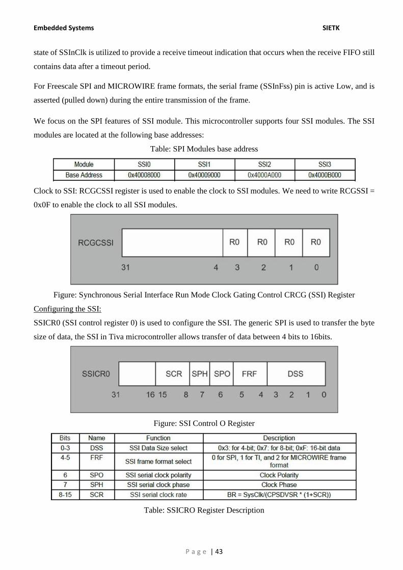
We focus on the SPI features of SSI module. This microcontroller supports four SSI modules. The SSI
modules are located at the following base addresses:
Table: SPI Modules base address
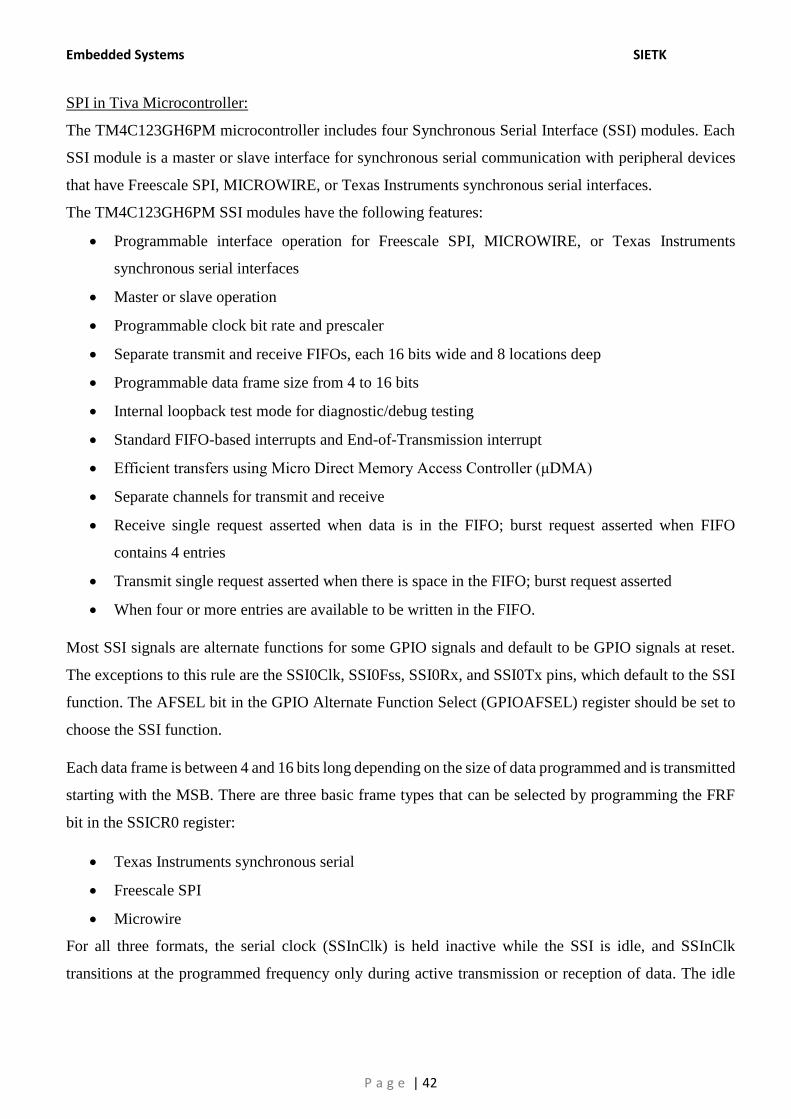
Clock to SSI: RCGCSSI register is used to enable the clock to SSI modules. We need to write RCGSSI =
0x0F to enable the clock to all SSI modules.
Figure: Synchronous Serial Interface Run Mode Clock Gating Control CRCG (SSI) Register
Configuring the SSI:
SSICR0 (SSI control register 0) is used to configure the SSI. The generic SPI is used to transfer the byte
size of data, the SSI in Tiva microcontroller allows transfer of data between 4 bits to 16bits.
Figure: SSI Control O Register
Table: SSICRO Register Description
Embedded Systems SIETK
P a g e | 44
Bit Rate:
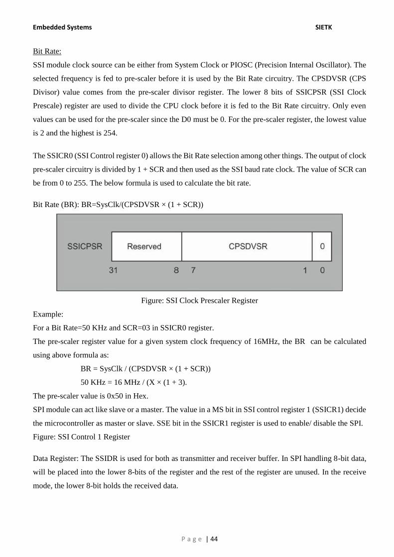
SSI module clock source can be either from System Clock or PIOSC (Precision Internal Oscillator). The
selected frequency is fed to pre-scaler before it is used by the Bit Rate circuitry. The CPSDVSR (CPS
Divisor) value comes from the pre-scaler divisor register. The lower 8 bits of SSICPSR (SSI Clock
Prescale) register are used to divide the CPU clock before it is fed to the Bit Rate circuitry. Only even
values can be used for the pre-scaler since the D0 must be 0. For the pre-scaler register, the lowest value
is 2 and the highest is 254.
The SSICR0 (SSI Control register 0) allows the Bit Rate selection among other things. The output of clock
pre-scaler circuitry is divided by 1 + SCR and then used as the SSI baud rate clock. The value of SCR can
be from 0 to 255. The below formula is used to calculate the bit rate.
Bit Rate (BR): BR=SysClk/(CPSDVSR × (1 + SCR))
Figure: SSI Clock Prescaler Register
Example:
For a Bit Rate=50 KHz and SCR=03 in SSICR0 register.
The pre-scaler register value for a given system clock frequency of 16MHz, the BR can be calculated
using above formula as:
BR = SysClk / (CPSDVSR × (1 + SCR))
50 KHz = 16 MHz / (X × (1 + 3).
The pre-scaler value is 0x50 in Hex.
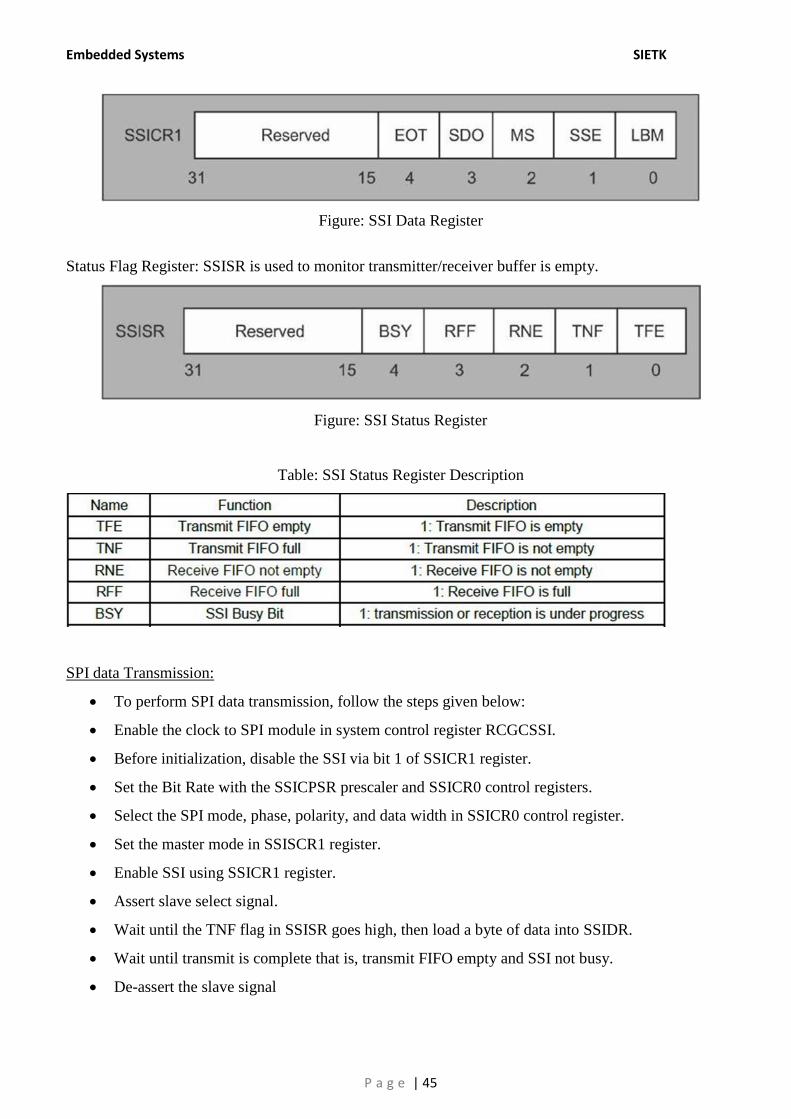
SPI module can act like slave or a master. The value in a MS bit in SSI control register 1 (SSICR1) decide
the microcontroller as master or slave. SSE bit in the SSICR1 register is used to enable/ disable the SPI.
Figure: SSI Control 1 Register
Data Register: The SSIDR is used for both as transmitter and receiver buffer. In SPI handling 8-bit data,
will be placed into the lower 8-bits of the register and the rest of the register are unused. In the receive
mode, the lower 8-bit holds the received data.
Embedded Systems SIETK
P a g e | 45
Figure: SSI Data Register
Status Flag Register: SSISR is used to monitor transmitter/receiver buffer is empty.
Figure: SSI Status Register
Table: SSI Status Register Description
SPI data Transmission:
• To perform SPI data transmission, follow the steps given below:
• Enable the clock to SPI module in system control register RCGCSSI.
• Before initialization, disable the SSI via bit 1 of SSICR1 register.
• Set the Bit Rate with the SSICPSR prescaler and SSICR0 control registers.
• Select the SPI mode, phase, polarity, and data width in SSICR0 control register.
• Set the master mode in SSISCR1 register.
• Enable SSI using SSICR1 register.
• Assert slave select signal.
• Wait until the TNF flag in SSISR goes high, then load a byte of data into SSIDR.
• Wait until transmit is complete that is, transmit FIFO empty and SSI not busy.
• De-assert the slave signal
Embedded Systems SIETK
P a g e | 46
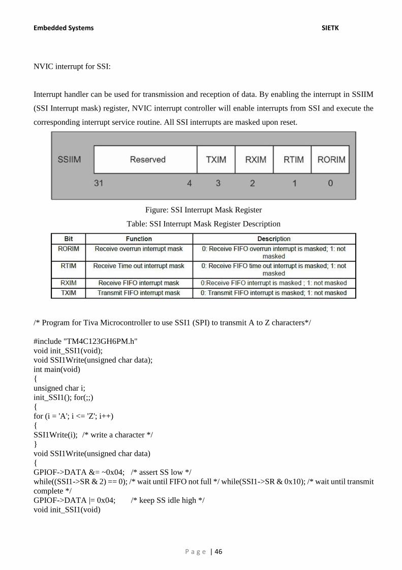
NVIC interrupt for SSI:
Interrupt handler can be used for transmission and reception of data. By enabling the interrupt in SSIIM
(SSI Interrupt mask) register, NVIC interrupt controller will enable interrupts from SSI and execute the
corresponding interrupt service routine. All SSI interrupts are masked upon reset.
Figure: SSI Interrupt Mask Register
Table: SSI Interrupt Mask Register Description
/* Program for Tiva Microcontroller to use SSI1 (SPI) to transmit A to Z characters*/
#include "TM4C123GH6PM.h"
void init_SSI1(void);
void SSI1Write(unsigned char data);
int main(void)
{
unsigned char i;
init_SSI1(); for(;;)
{
for (i = 'A'; i <= 'Z'; i++)
{
SSI1Write(i); /* write a character */
}
void SSI1Write(unsigned char data)
{
GPIOF->DATA &= ~0x04; /* assert SS low */
while((SSI1->SR & 2) == 0); /* wait until FIFO not full */ while(SSI1->SR & 0x10); /* wait until transmit
complete */
GPIOF->DATA |= 0x04; /* keep SS idle high */
void init_SSI1(void)
Embedded Systems SIETK
P a g e | 47
{
SYSCTL->RCGCSSI |= 2; /* enable clock to SSI1 */
/* configure PORTD 3, 1 for SSI1 clock and Tx */
GPIOD->DEN |= 0x09; /* and make them digital */
GPIOD->AFSEL |= 0x09; /* enable alternate function */
GPIOD->PCTL &= ~0x0000F00F; /* assign pins to SSI1 */
GPIOD->PCTL |= 0x00002002; /* assign pins to SSI1 */
/* configure PORTF 2 for slave select */
GPIOF->DEN |= 0x04; /* make the pin digital */
GPIOF->DIR |= 0x04; /* make the pin output */
GPIOF->DATA |= 0x04; /* keep SS idle high */
/* SPI Master, POL = 0, PHA = 0, clock = 4 MHz, 16 bit data */
SSI1->CR1 = 0; /* disable SSI and make it master */
SSI1->CC = 0; /* use system clock */
SSI1->CPSR = 2; /* prescaler divided by 2 */
SSI1->CR1 |= 2; /* enable SSI1 */
}
void SystemInit(void)
{
SCB->CPACR |= 0x00f00000;
}
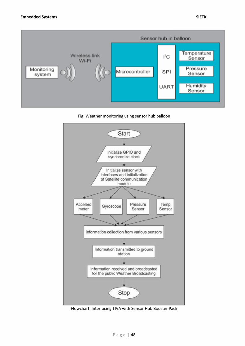
Case Study: Tiva based embedded system application using the interface protocols for communication with external devices “Sensor Hub BoosterPack”
Weather monitoring balloon using sensor hub:
Microcontrollers or System on Chips (SoC) are important components of modern day electronic systems.
But microcontrollers alone can’t make systems. Microcontrollers need to communicate with other devices
on the same PCB or with devices of other PCB from the same system, to achieve the system functionality
in applications such as digital audio, digital signal processing, or telecommunications channels.
Microcontroller is an intelligent component on the system, which runs the software program to take
decisions and control the other components of the system.
Consider a system shown in Fig below, which highlight the various components of weather monitoring
systems. The weather monitoring systems usually monitor atmospheric properties such as humidity,
temperature, pressure etc. The various parameters are gathered using sensors that are interfaced with
microcontroller using popular serial interfaces such as SPI, I2C, and UART etc. The same system can be
used for upper atmospheric data gathering missions by incorporating Wi-Fi and satellite connectivity with
the ground station. Therefore, communication between microcontroller and other devices on the system
is very important to achieve intended functionality.
Embedded Systems SIETK
P a g e | 48
Fig: Weather monitoring using sensor hub balloon
Flowchart: Interfacing TIVA with Sensor Hub Booster Pack
Embedded Systems SIETK
P a g e | 49
Weather broadcasting system require some smart technique to monitor the weather conditions of
different places. It is useful for the meteorological department for the detection of the environmental
condition with the help of a balloon. In this case study we are using four sensors Accelerometer,
gyroscope, temperature sensor and pressure sensor. The Tiva booster pack with various sensors is
mounted on the balloon and accelerometer used for the detection of acceleration of the balloon and gyro
scope is used for the position detection of the balloon and pressure and temperature sensor senses pressure
and temperature of the environment respectively. These all gathered information sent to the ground station
with the help of satellite communication system installed at the balloon and the meteorological
department’s ground station. The collected information is used for the public weather broadcasting.
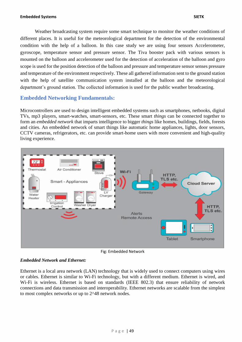
Embedded Networking Fundamentals:
Microcontrollers are used to design intelligent embedded systems such as smartphones, netbooks, digital
TVs, mp3 players, smart-watches, smart-sensors, etc. These smart things can be connected together to
form an embedded network that imparts intelligence to bigger things like homes, buildings, fields, forests
and cities. An embedded network of smart things like automatic home appliances, lights, door sensors,
CCTV cameras, refrigerators, etc. can provide smart-home users with more convenient and high-quality
living experience.
Fig: Embedded Network
Embedded Network and Ethernet:
Ethernet is a local area network (LAN) technology that is widely used to connect computers using wires
or cables. Ethernet is similar to Wi-Fi technology, but with a different medium. Ethernet is wired, and
Wi-Fi is wireless. Ethernet is based on standards (IEEE 802.3) that ensure reliability of network
connections and data transmission and interoperability. Ethernet networks are scalable from the simplest
to most complex networks or up to 2^48 network nodes.
Embedded Systems SIETK
P a g e | 50
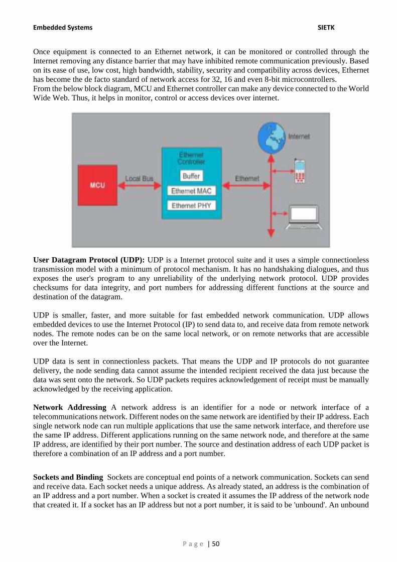
Once equipment is connected to an Ethernet network, it can be monitored or controlled through the
Internet removing any distance barrier that may have inhibited remote communication previously. Based
on its ease of use, low cost, high bandwidth, stability, security and compatibility across devices, Ethernet
has become the de facto standard of network access for 32, 16 and even 8-bit microcontrollers.
From the below block diagram, MCU and Ethernet controller can make any device connected to the World
Wide Web. Thus, it helps in monitor, control or access devices over internet.
User Datagram Protocol (UDP): UDP is a Internet protocol suite and it uses a simple connectionless
transmission model with a minimum of protocol mechanism. It has no handshaking dialogues, and thus
exposes the user's program to any unreliability of the underlying network protocol. UDP provides
checksums for data integrity, and port numbers for addressing different functions at the source and
destination of the datagram.
UDP is smaller, faster, and more suitable for fast embedded network communication. UDP allows
embedded devices to use the Internet Protocol (IP) to send data to, and receive data from remote network
nodes. The remote nodes can be on the same local network, or on remote networks that are accessible
over the Internet.
UDP data is sent in connectionless packets. That means the UDP and IP protocols do not guarantee
delivery, the node sending data cannot assume the intended recipient received the data just because the
data was sent onto the network. So UDP packets requires acknowledgement of receipt must be manually
acknowledged by the receiving application.
Network Addressing A network address is an identifier for a node or network interface of a
telecommunications network. Different nodes on the same network are identified by their IP address. Each
single network node can run multiple applications that use the same network interface, and therefore use
the same IP address. Different applications running on the same network node, and therefore at the same
IP address, are identified by their port number. The source and destination address of each UDP packet is
therefore a combination of an IP address and a port number.
Sockets and Binding Sockets are conceptual end points of a network communication. Sockets can send
and receive data. Each socket needs a unique address. As already stated, an address is the combination of
an IP address and a port number. When a socket is created it assumes the IP address of the network node
that created it. If a socket has an IP address but not a port number, it is said to be 'unbound'. An unbound
Embedded Systems SIETK
P a g e | 51
socket cannot receive data because it does not have a complete address. When a socket has both an IP
address and a port number it is said to be 'bound to a port', or 'bound to an address'. A bound socket can
receive data because it has a complete address. The process of allocating a port number to a socket is
called 'binding'.
Client and Server Servers are applications that wait for and then reply to incoming requests. Clients are
applications that send requests to servers. In this context, the requests and replies go over the network and
clients need to locate servers. Servers do not need to know the client's address in advance, they just send
their replies to the address from which the client's request originated and therefore clients can bind to
nearly any port number.
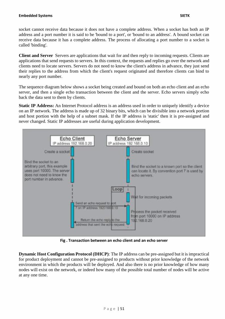
The sequence diagram below shows a socket being created and bound on both an echo client and an echo
server, and then a single echo transaction between the client and the server. Echo servers simply echo
back the data sent to them by clients.
Static IP Address: An Internet Protocol address is an address used in order to uniquely identify a device
on an IP network. The address is made up of 32 binary bits, which can be divisible into a network portion
and host portion with the help of a subnet mask. If the IP address is 'static' then it is pre-assigned and
never changed. Static IP addresses are useful during application development.
Fig . Transaction between an echo client and an echo server
Dynamic Host Configuration Protocol (DHCP): The IP address can be pre-assigned but it is impractical
for product deployment and cannot be pre-assigned to products without prior knowledge of the network
environment in which the products will be deployed. And also there is no prior knowledge of how many
nodes will exist on the network, or indeed how many of the possible total number of nodes will be active
at any one time.
Embedded Systems SIETK
P a g e | 52
DHCP provides an alternative to static IP address assignment. DHCP servers exist on local networks to
dynamically allocate IP addresses to nodes on the same network. When a network enabled product boots
up it contacts the DHCP server to request its IP address, removing the need for each node to be statically
configured.
Sub-netting / Netmask: A subnetwork, or subnet, is a logical, visible subdivision of an IP network. The
practice of dividing a network into two or more networks is called sub-netting. Sub-netting is a way of
determining whether a destination IP address exists on the local network or a remote network. Like the IP
address, the subnet mask can be configured either statically or dynamically from a DHCP server. If a
destination IP address bitwise ANDed with the subnet mask matches the local IP address bitwise ANDed
with the subnet mask then the two IP addresses exist on the same network.
Gateways and Routers: A gateway acts as a conversion from one protocol to another. A router works by
looking at the IP address in the data packet and decides if it is for internal use or if the packet should move
outside the network. If a destination IP address bitwise ANDed with the subnet mask does not match the
local IP address bitwise ANDed with the subnet mask then the two IP addresses do not exist on the same
network. In this case the packet being sent to the destination address cannot be sent directly, and must
instead be sent to a gateway for intelligent inter-network routing.
Domain Name System (DNS): The Domain Name System (DNS) is a hierarchical distributed naming
system for computers, services, or any resource connected to the Internet or a private network. It associates
various information with domain names assigned to each of the participating entities. Most prominently,
it translates domain names, which can be easily memorized by humans, to the numerical IP addresses
needed for the purpose of computer services and devices worldwide. The Domain Name System is an
essential component of the functionality of most Internet services because it is the Internet's primary
directory service.
For example, entering "ping www.freertos.org" in the command console of a desktop computer will show
a ping request being sent to the IP address 195.8.66.1 (today anyway) a DNS server resolved the string
"www.freertos.org" to the IP address 195.8.66.1.
Address Resolution Protocol (ARP): The Address Resolution Protocol (ARP) is a telecommunication
protocol used for resolution of network layer addresses into link layer addresses, a critical function in
multiple-access networks. Assuming a conventional wired network is used, UDP messages are sent in
Ethernet frames. UDP messages are sent between IP addresses, but Ethernet frames are sent between
MAC (hardware) addresses. Therefore, the MAC address of the destination IP address must be known
before an Ethernet frame can be created. The Address Resolution Protocol (ARP) is used to obtain MAC
address information.
TCP/IP Introduction IoT overview and architecture:
Communication between computers or embedded devices in a network involves exchanging useful
messages over a medium like air, telephone line, Ethernet, etc. Each device must have an address or ID
using which, it can be uniquely identified in the network. The devices must follow some rules while
communicating with each other, so that messages are exchanged in a proper manner. IP (Internet Protocol)
provides a set of unique addresses to the devices, whereas TCP (Transport Control Protocol) describes a
set of rules to be followed to exchange messages in a proper way.
Embedded Systems SIETK
P a g e | 53
In the smart home application shown in fig. below, TCP/IP protocol can be used over Ethernet to provide
Internet connectivity to the outside world. This will enable the user to monitor or control the smart home
functions from anywhere in the world using a PC, laptop or a smartphone.
Internet Protocol version 6 (IPv6):
IPv6 is the most recent version of the Internet Protocol (IP), the communications protocol that provides
an identification and location system for computers on networks and routes traffic across the Internet.
IPv6 advantages for IoT:
Adoption: The Internet Protocol is a must and a requirement for any Internet connectivity. It is the
addressing scheme for any data transfer on the web.
Scalability: IPv6 offers a highly scalable address scheme. The present scheme of Internet Governance
provides at most 2 x 10¹⁹ unique, globally routable, addresses.
Solving the NAT barrier: The Network Address Translation (NAT). It enables several users and
devices to share the same public IP address. The NAT users are borrowing and sharing IP addresses with
others.
Multi-Stakeholder Support: IPv6 provides for end devices to have multiple addresses. Multiple
stakeholders can deploy their own applications, sharing a common sensor/actuation infrastructure, without
impacting the technical operation or governance of the Internet.
Internet of Things (IOT):
Klevin Ashton introduced the term “Internet of Things” (IOT), to the world of technology in 1999. All
the real-life things (including objects, people and animals) are connected to internet, and can transfer data
over it preferably to a cloud. This data can then be used by businesses and the people, to create a world of
new possibilities and to benefit from it. Fig. below shows the three main components of IoT i.e. things,
data (cloud) and the people. For e.g. a smart refrigerator can sense the quantity of items inside it, and then
automatically generate a shopping list to be ordered on-line. This list is put by the smart refrigerator on
the cloud, where the best deals are offered for online purchase.
IOT is considered as a scenario of accessing any information from anywhere and accessible to
everyone. This is described as follows:
Anything: Eventually, any device, appliance or entity will be seamlessly connected to the Internet.
Connectivity will not be the main feature of the device, but will extend the device capabilities.
Anywhere: Any conceived wireless connectivity framework should be abstract enough to run from
any location.
Anyone: IoT accessible to anyone. Anyone will be able to connect their product to the Internet, and
also customize it to their personal preferences.
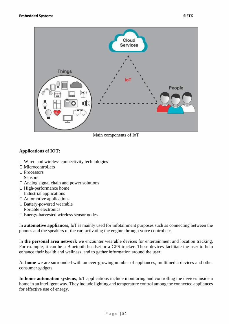
Embedded Systems SIETK
P a g e | 54
Main components of IoT
Applications of IOT:
Wired and wireless connectivity technologies
Microcontrollers
Processors
Sensors
Analog signal chain and power solutions
High-performance home
Industrial applications
Automotive applications
Battery-powered wearable
Portable electronics
Energy-harvested wireless sensor nodes.
In automotive appliances, IoT is mainly used for infotainment purposes such as connecting between the
phones and the speakers of the car, activating the engine through voice control etc.
In the personal area network we encounter wearable devices for entertainment and location tracking.
For example, it can be a Bluetooth headset or a GPS tracker. These devices facilitate the user to help
enhance their health and wellness, and to gather information around the user.
At home we are surrounded with an ever-growing number of appliances, multimedia devices and other
consumer gadgets.
In home automation systems, IoT applications include monitoring and controlling the devices inside a
home in an intelligent way. They include lighting and temperature control among the connected appliances
for effective use of energy.
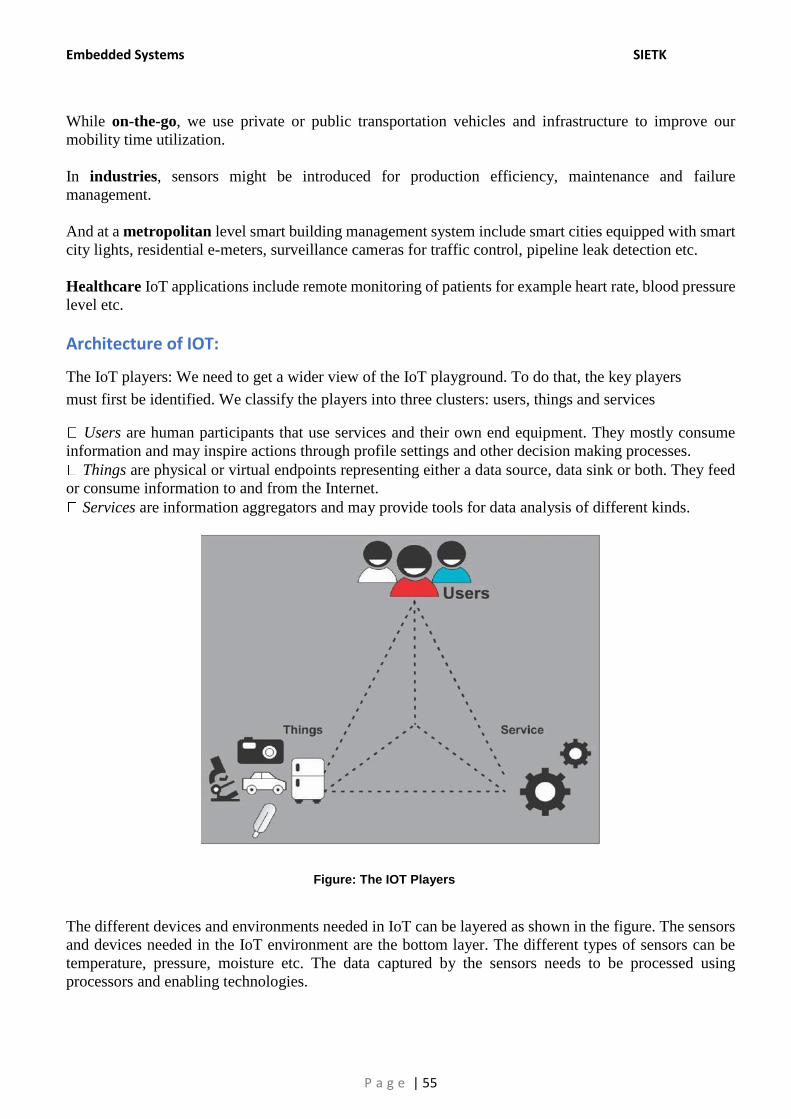
Embedded Systems SIETK
P a g e | 55
While on-the-go, we use private or public transportation vehicles and infrastructure to improve our
mobility time utilization.
In industries, sensors might be introduced for production efficiency, maintenance and failure
management.
And at a metropolitan level smart building management system include smart cities equipped with smart
city lights, residential e-meters, surveillance cameras for traffic control, pipeline leak detection etc.
Healthcare IoT applications include remote monitoring of patients for example heart rate, blood pressure
level etc.
Architecture of IOT:
The IoT players: We need to get a wider view of the IoT playground. To do that, the key players
must first be identified. We classify the players into three clusters: users, things and services
Users are human participants that use services and their own end equipment. They mostly consume
information and may inspire actions through profile settings and other decision making processes.
Things are physical or virtual endpoints representing either a data source, data sink or both. They feed
or consume information to and from the Internet.
Services are information aggregators and may provide tools for data analysis of different kinds.
Figure: The IOT Players
The different devices and environments needed in IoT can be layered as shown in the figure. The sensors
and devices needed in the IoT environment are the bottom layer. The different types of sensors can be
temperature, pressure, moisture etc. The data captured by the sensors needs to be processed using
processors and enabling technologies.
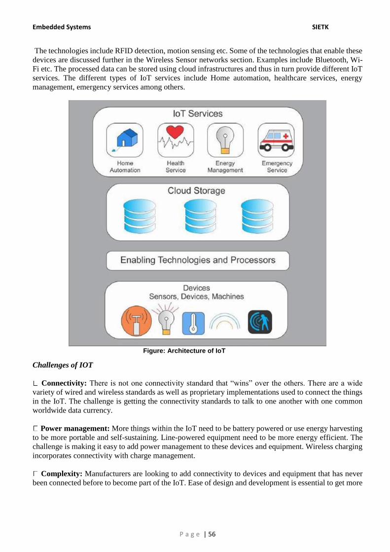
Embedded Systems SIETK
P a g e | 56
The technologies include RFID detection, motion sensing etc. Some of the technologies that enable these
devices are discussed further in the Wireless Sensor networks section. Examples include Bluetooth, Wi-
Fi etc. The processed data can be stored using cloud infrastructures and thus in turn provide different IoT
services. The different types of IoT services include Home automation, healthcare services, energy
management, emergency services among others.
Figure: Architecture of IoT
Challenges of IOT
Connectivity: There is not one connectivity standard that “wins” over the others. There are a wide
variety of wired and wireless standards as well as proprietary implementations used to connect the things
in the IoT. The challenge is getting the connectivity standards to talk to one another with one common
worldwide data currency.
Power management: More things within the IoT need to be battery powered or use energy harvesting
to be more portable and self-sustaining. Line-powered equipment need to be more energy efficient. The
challenge is making it easy to add power management to these devices and equipment. Wireless charging
incorporates connectivity with charge management.
Complexity: Manufacturers are looking to add connectivity to devices and equipment that has never
been connected before to become part of the IoT. Ease of design and development is essential to get more
Embedded Systems SIETK
P a g e | 57
things connected especially when typical RF programming is complex. Additionally, the average
consumer needs to be able to set-up and use their devices without a technical background
Rapid evolution: The IoT is constantly changing and evolving. More devices are being added every
day. The challenge facing the industry is the unknown; unknown devices, unknown applications, unknown
use cases. There needs to be flexibility in development.
Energy Efficiency: When it comes to power, the challenge is to ensure that adding Internet connectivity
does not impose a change to the power supply. In other words, ideally it should fit within the existing
power budget headroom.
Security: Security is always a challenge in data networks. This challenge intensifies in the case of the
IoT simply because there are more entry points thereby creating more penetration points. This increased
system vulnerability makes the battle for security inevitable. In an IoT solution, threats also take a new
level of magnitude since it is not just data that is put at risk. With IoT the damage potential is much higher
(e.g., opening a door remotely, taking a burglar alarm system offline). There will surely be a never-ending
fight towards better security. This provides inbuilt security features to address major security
requirements.
Data handling: Massive deployment of endpoints results in higher node density. This requires demand
for higher capacity. Furthermore, large quantities of data that are generated create a need for accessible
storage. In addition, real network latency introduces a challenge to limited resource systems.
Wireless Sensor Networks:
Wireless Sensor Networks (WSNs) are networks of tiny, battery powered sensor nodes with limited
onboard processing, storage and radio capabilities. Recent advances in micro-electro-mechanical systems
(MEMS) technology, embedded electronics and wireless communication have made it possible to develop
low-power and low-cost sensor nodes that are small in size and communicate using wireless medium over
short distances.
The sensor units in the nodes can sense any desired parameter (like temperature, pressure humidity,
movement etc.) in an area that is covered by the network. The sensed data is then relayed through the
network to the base station, where information can be generated and acted upon to serve the purpose for
which the network has been deployed.
WSNs are on the verge of being utilized for many challenging real-life applications like early earthquake
warning systems, battlefield surveillance, environment and habitat monitoring, healthcare, smart homes
and buildings etc... This involves deploying a large number of nodes in the area to be sensed by the
network. This large-scale deployment often requires the nodes to possess self-organizing capability to
form a network without any human intervention.
A typical cluster-based sensor network topology as shown in Fig. 5.10 consists of a base station, cluster-
head nodes and sensor nodes. The base station is normally connected to the outside world through internet
link or a user terminal.
Embedded Systems SIETK
P a g e | 58
Fig . A Typical Sensor Network Architecture
Wireless Connectivity in Embedded Networks:
Wireless communication has become a preferred choice for connecting the devices in embedded networks.
Communication technologies like NFC, ZigBee, Bluetooth, WiFi, and cellular have already become popular
with developers working on Smart Homes, Sensor Networks and IoT based applications. The choice of a
connectivity option depends upon various factors like communication range, bandwidth requirements, security
issues, and power consumption.
Fig. Comparison of different wireless technologies
Embedded Systems SIETK
P a g e | 59
Near Field Communication (NFC):
NFC is a wireless communication technology that enables two devices to interact when they are in very
close proximity to each other. For example, smartphones and other such devices can use NFC to interact
with NFC-enabled machines (for e.g. battery-charging portals, ticket-vending machines, ATM, etc.) to
exchange information at a distance of less than 10cm. NFC-enabled devices use globally available
unlicensed radio frequency ISM band of 13.56 MHz on standard ISO/IEC 18000-3 air interface at rates
ranging from 106 kbit/s to 424 kbit/s. Each full NFC device can work in 3 modes:
1. NFC Card Emulation mode – devices act like smart cards, to allow users to perform transactions like
payment or ticketing.
2. NFC Reader/ Writer mode – allows NFC-enabled devices to read information stored on NFC tags
embedded in labels or smart posters.
3. NFC Peer-to-peer mode – NFC-enabled devices can form an adhoc network to communicate and
exchange information with each other.
ZigBee:
ZigBee is an industry-standard wireless networking technology that is suitable for applications that require
infrequent low-power data transfer at low data rates within a 100m range, such as inside a home or a
building. It is an IEEE 802.15.4 based specification for a suite of high-level communication protocols
used to create personal area networks (PAN’s) with small, low-power digital radios.
ZigBee based PAN’s are suitable for applications like - home entertainment and control, building
automation, industrial control and implementing wireless sensor networks. It operates in the ISM radio
bands with data rates that can vary from 20 kbit/s to 250 kbit/s. The protocol stack for ZigBee builds on
the physical layer and MAC layer defined in IEEE standard 802.15.4 for low-rate wireless PAN’s
(WPAN’s). To this, ZigBee adds on specifications for network layer and application layer.
The ZigBee network layer supports star,tree and mesh network topologies. The application layer provides
an interface between ZigBee system and the end user applications. A ZigBee network may consist of the
following three types of devices:
Fig 5.42. Zigbee co-ordinator with end device
Embedded Systems SIETK
P a g e | 60
ZigBee Coordinator (ZC): It is the most capable device in the network. Each ZigBee network must
have exactly one coordinator device, and it is responsible to build and maintain the network. The ZC
forms the root of the network and also connects to the other networks.
ZigBee Router (ZR): In addition to communicating with ZC, a ZR device can perform the function of
forwarding/routing data received from other devices.
ZigBee End Device (ZED): A ZED device can only talk to its parent node, a ZC or a ZR device.
Bluetooth
It is an important short-range communication technology that is widely used in smartphones and many other
fixed as well as mobile devices, for data transfer and building personal area networks. It operates in the 2.4
GHz ISM frequency band and uses frequency hopping spread spectrum technique. Bluetooth is a packet-based
protocol with a master-slave structure. One master may communicate with upto 7 slaves in a piconet. Two or
more piconets can be connected to form a bigger network, called a scatternet.
Bluetooth is widely used in applications like handsfree headset, smartphone-to-smartphone data transfer,
wireless communication between smartphone and car-stereo system, cable-free connection between PC and
I/O modules like mouse, keyboard, printer etc. Bluetooth in its new avatar as Bluetooth Low Energy (BLE) or
Bluetooth Smart, is expected to be a key technology in near future for wearable devices that will connect to
the IoT, probably through the smartphones and other such options.
Bluetooth Smart is meant to provide low-cost and low-power consumption while maintaining the same range
as Bluetooth. Application development with Bluetooth Smart: Texas Instrument’s CC2460 is a wireless MCU
that can be used to design Bluetooth Smart enabled applications. The CC2640 contains a 32-bit ARM Cortex-
M3 processor running at 48- MHz as the main processor and a rich peripheral feature set, including a unique
ultra-low power sensor controller, ideal for interfacing external sensors and/or collecting analog and digital
data autonomously while the rest of the system is in sleep mode. The Bluetooth Low Energy controller is
embedded into ROM and run partly on an ARM Cortex®-M0 processor.
Wi-Fi
Wi-Fi is a wireless local area network (WLAN) technology that allows electronic devices to network using the
2.4 GHz or 5 GHz ISM radio bands. It is based on the IEEE 802.11 MAC and physical layer standards for
WLAN and is the most pervasive choice for connectivity with the Internet, especially in the home LAN
environment. Wi-Fi supports very fast data transfer rates, but consumes a lot of power which makes it unviable
for low-power applications. Nevertheless, the embedded networks, wireless sensor network applications and
Internet-of-Things implementations explicitly make use of Wi-Fi as a preferred choice for connectivity to the
Internet.
Adding Wi-fi to a Microcontroller-Based System using CC3100 Simple
link Wi-fi Module:
To illustrate the use of wireless connectivity in embedded networks, this section discusses the usage of Wi-Fi
technology with a microcontroller. Wi-Fi is very widely used to provide connectivity between user and
embedded systems. For example, a user can interact with utility systems (like AC, Garage door, Coffee
machine, etc.) in a smart-home using a smartphone, provided both (smart-home and smartphone) are connected
to the internet. TI provides low-power and easy-to-use Wi-Fi solutions that include battery-operated Wi-Fi
designs with more than a year of battery life on two AA batteries. TI’s Simple Link Wi-Fi CC3100 module is
a wireless network processor with on-chip Wi-Fi, internet, and robust security protocols. It can be used to
connect any low-cost microcontroller (MCU).
Embedded Systems SIETK
P a g e | 61
Fig Functional diagram of SimpleLink Wi-Fi CC3100 Module
Fig SimpleLink Wi-Fi CC3100 Module
Embedded Wi-Fi:
Architecture of Simple Link Wi-Fi CC3100 Module
It is important to understand the hardware and software architecture of any device before using it in a design.
Fig. shows the hardware architecture for Simple Link Wi-Fi CC3100 module, that can be used to provide Wi-
Fi connectivity to any micro-controller based system. It consists mainly of two parts:
I. Wi-Fi Network Processor Subsystem
II. Power-management Subsystem
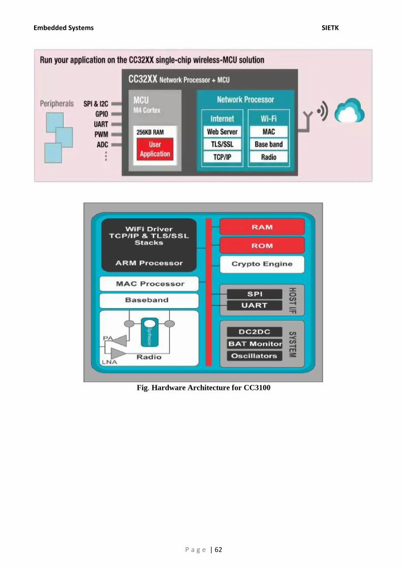
Embedded Systems SIETK
P a g e | 62
Fig. Hardware Architecture for CC3100
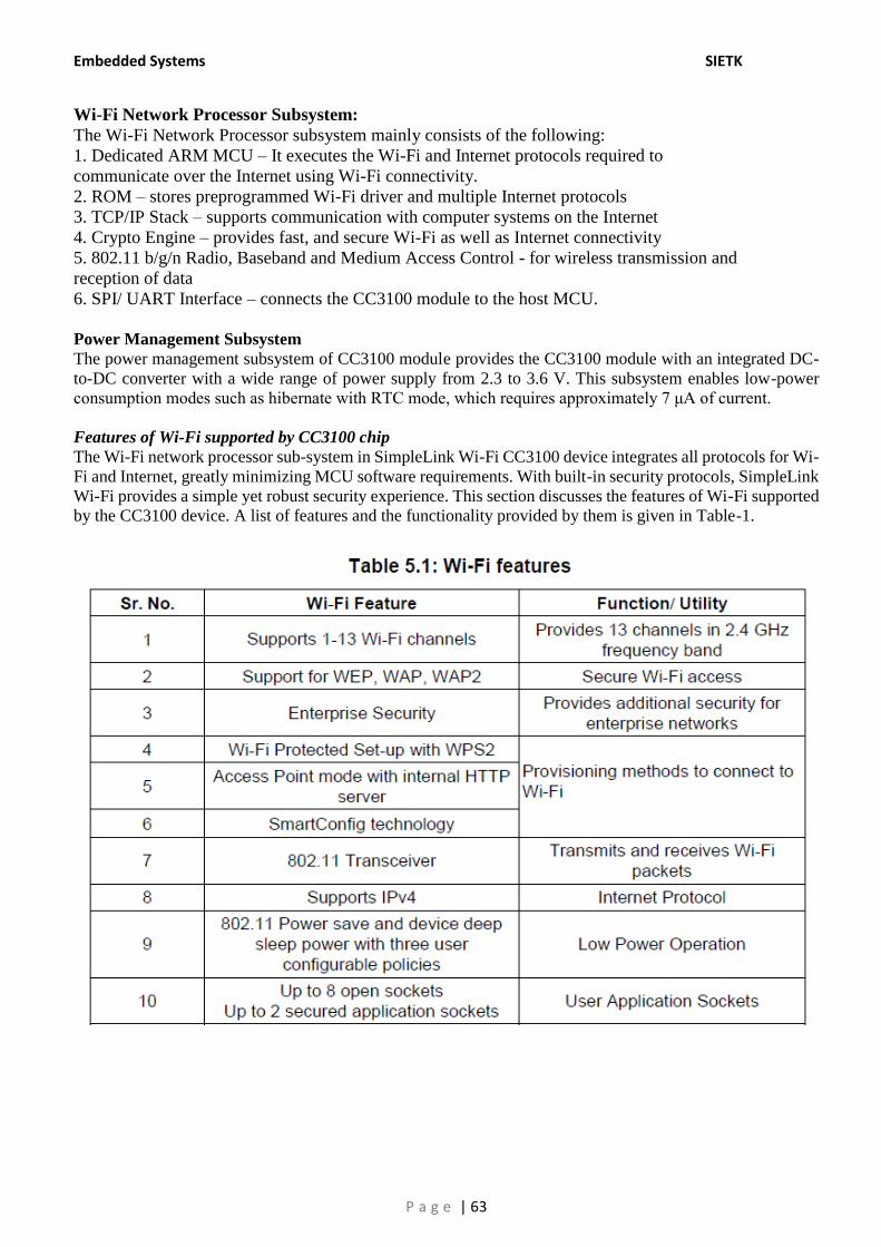
Embedded Systems SIETK
P a g e | 63
Wi-Fi Network Processor Subsystem:
The Wi-Fi Network Processor subsystem mainly consists of the following:
1. Dedicated ARM MCU – It executes the Wi-Fi and Internet protocols required to
communicate over the Internet using Wi-Fi connectivity.
2. ROM – stores preprogrammed Wi-Fi driver and multiple Internet protocols
3. TCP/IP Stack – supports communication with computer systems on the Internet
4. Crypto Engine – provides fast, and secure Wi-Fi as well as Internet connectivity
5. 802.11 b/g/n Radio, Baseband and Medium Access Control - for wireless transmission and
reception of data
6. SPI/ UART Interface – connects the CC3100 module to the host MCU.
Power Management Subsystem
The power management subsystem of CC3100 module provides the CC3100 module with an integrated DC-
to-DC converter with a wide range of power supply from 2.3 to 3.6 V. This subsystem enables low-power
consumption modes such as hibernate with RTC mode, which requires approximately 7 μA of current.
Features of Wi-Fi supported by CC3100 chip
The Wi-Fi network processor sub-system in SimpleLink Wi-Fi CC3100 device integrates all protocols for Wi-
Fi and Internet, greatly minimizing MCU software requirements. With built-in security protocols, SimpleLink
Wi-Fi provides a simple yet robust security experience. This section discusses the features of Wi-Fi supported
by the CC3100 device. A list of features and the functionality provided by them is given in Table-1.
Embedded Systems SIETK
P a g e | 64
USER APIs:
CC3100 SimpleLink Driver and its Application Programming Interface (API)
In order to simplify the development using the SimpleLink Wi-Fi devices, TI provides a simple and user
friendly host driver software. This driver software allows any MCU (like TIVA platform) to interact with
a SimpleLink device and performs the following functions:
1. Provides a simple API for user application development.
2. Handles the communication of MCU with the SimpleLInk device.
3. Provides flexibility in working with a MCU, with or without an OS.
4. Works with existing UART or SPI physical interface drivers
5. Compatible with 8-bit, 16-bit or 32-bit MCUs
The SimpleLink Host Driver includes a set of six logical and simple API modules:
Device API – Manages hardware-related functionality such as start, stop, set, and get device
configurations.
WLAN API – Manages WLAN, 802.11 protocol-related functionality such as device mode (station,
AP, or P2P), setting provisioning method, adding connection profiles, and setting connection policy.
Socket API – The most common API set for user applications, and adheres to BSD socket APIs.
NetApp API – Enables different networking services including the Hypertext Transfer Protocol
(HTTP) server service, DHCP server service, and MDNS client\server service.
NetCfg API – Configures different networking parameters, such as setting the MAC address, acquiring
the IP address by DHCP, and setting the static IP address.
File System API – Provides access to the serial flash component for read and write operations of
networking or user proprietary data.
Programmer’s model for CC3100 SimpleLink driver and its API
A programmer using a SimpleLink device needs to know about the different software blocks needed to
build a networking application. This topic describes the recommended flow for most applications.
However, program developers have complete flexibility on how to use the various software blocks.
Programs using the SimpleLink device consist of the following software blocks:
o Wi-Fi subsystem initialization – Wakes the Wi-Fi subsystem from the hibernate state.
o Configuration – WiFi sub-system. This phase refers to time configuration that does not happen very
often. For instance, changing the WiFi sub-system from a WLAN STA to WLAN soft AP, changing the
MAC address and so forth.
o WLAN connection – The physical interface needs to be established. There are numerous ways to do
so, all of which will be explained in this document. The simplest way is to manually connect to an AP as
a wireless station.
DHCP – Although not an integral part of the WLAN connection, you need to wait for the receiving
IP address before continuing to the next step of working with TCP\UDP sockets.
o Socket connection – At this point, it is up to the application to set up their TCP\IP layer. Separate this
phase into the following parts:
Creating the socket – Choosing to use TCP, UDP or RAW sockets, whether to use a client or a server
socket, defining socket characteristics such as blocking\nonblocking, socket timeouts, and so forth.
Querying for the server IP address – In most occasions, when implementing a client side
communication, you will not know the remote server side IP address, which is required for establishing
the socket connection. This can be done by using DNS protocol to query the server IP address by using
the server name.
Embedded Systems SIETK
P a g e | 65
Creating socket connection – When using the TCP socket, it is required to establish a proper socket
connection before continuing to perform data transaction.
o Data transactions – Once the socket connection was established, it is possible to transmit data both
ways between the client and the server. Basically implementing the application logic.
o Socket disconnection – Upon finishing the required data transactions, it is recommended to perform a
graceful closure of the socket communication channel.
o Wi-Fi subsystem hibernate – When not working with the Wi-Fi subsystem for a long period of time,
it is recommended to put it into hibernate mode.
Case Studies with SimpleLink Wi-Fi CC3100 and TIVA Launchpad:-
Case Study: Smart Plug with Remote Disconnect and Wi-Fi Connectivity
In this application, the WiFi enabled Smart plug helps you to control any connected device from home or
remotely from anywhere in the world with internet access such as home appliances like control portable
heaters or window ac, turn on a light, Smart Grid and in building automation. A smart plug is an electronic
device, generally connected to other devices or networks via different wireless protocols such as
Bluetooth, NFC, WiFi, 3G, etc., that can operate to some extent interactively and autonomously. Now an
day all application like home automation and building automation requires two main aspects of Smart
Plug technology.
Android and cloud based remote access.
Remote disconnect and Wi-Fi connectivity based upon power consumption.
In this case study the WiFi enabled Smart Plug utilizes a TIVA Launchpad to monitor the energy
consumption for a single load and control the high-voltage side of the design. This data is then passed to
a CC3100 module to communicate the data over Wi-Fi to a Cloud server. A solid state relay enables the
application to control the load, based on its energy consumption. And this system is powered from a highly
compact and efficient UCC28910D High-Voltage Flyback Switcher with Primary-Side Regulation and
Output Current Control. Block Diagram
Figure shows a high-level overview of the connections between the the various devices in the Smart Plug
reference design. The only physical connections from the system are the AC voltage input and the output
for an AC load. On this high-voltage line, the flyback power supply, load control relay, and metrology
sensors are connected. Circuit Design and Component Selection
Embedded Metrology – Analog Inputs
The analog front-end of the MSP430i204x, which consists of the ΣΔ ADC, is differential and requires
thatthe input voltages at the pins do not exceed ±928 mV (gain = 1). To meet this specification, the current
and voltage inputs must be scaled down. Additionally, the ΣΔ24 allows a maximum negative voltage of -
1V. Therefore, the AC current signal from mains can be directly interfaced without the need for level
shifters. This section describes the analog front end used for the voltage and current channels.
Voltage Inputs
The voltage from the mains is usually 230 V or 120 V, and must be scaled down to within 928 mV. The
analog front end for voltage consists of spike protection varistors followed by a voltage divider network,
and an RC low-pass filter that acts as an anti-alias filter.
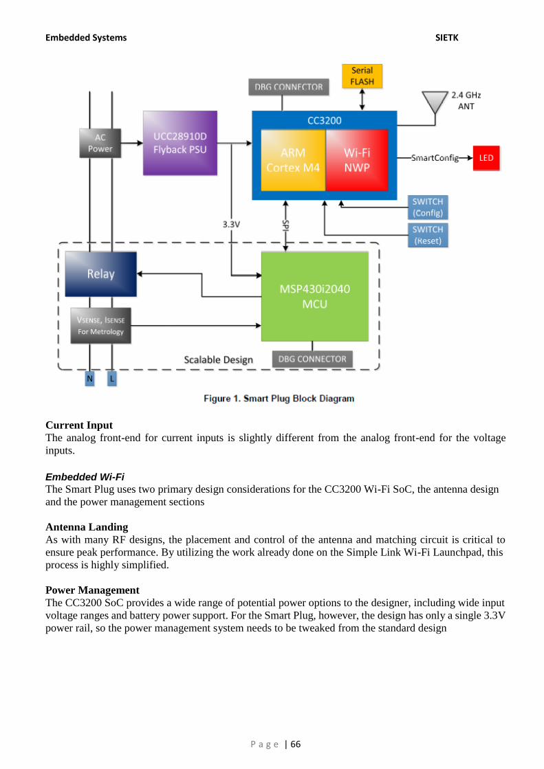
Embedded Systems SIETK
P a g e | 66
Current Input
The analog front-end for current inputs is slightly different from the analog front-end for the voltage
inputs.
Embedded Wi-Fi
The Smart Plug uses two primary design considerations for the CC3200 Wi-Fi SoC, the antenna design
and the power management sections
Antenna Landing
As with many RF designs, the placement and control of the antenna and matching circuit is critical to
ensure peak performance. By utilizing the work already done on the Simple Link Wi-Fi Launchpad, this
process is highly simplified.
Power Management
The CC3200 SoC provides a wide range of potential power options to the designer, including wide input
voltage ranges and battery power support. For the Smart Plug, however, the design has only a single 3.3V
power rail, so the power management system needs to be tweaked from the standard design
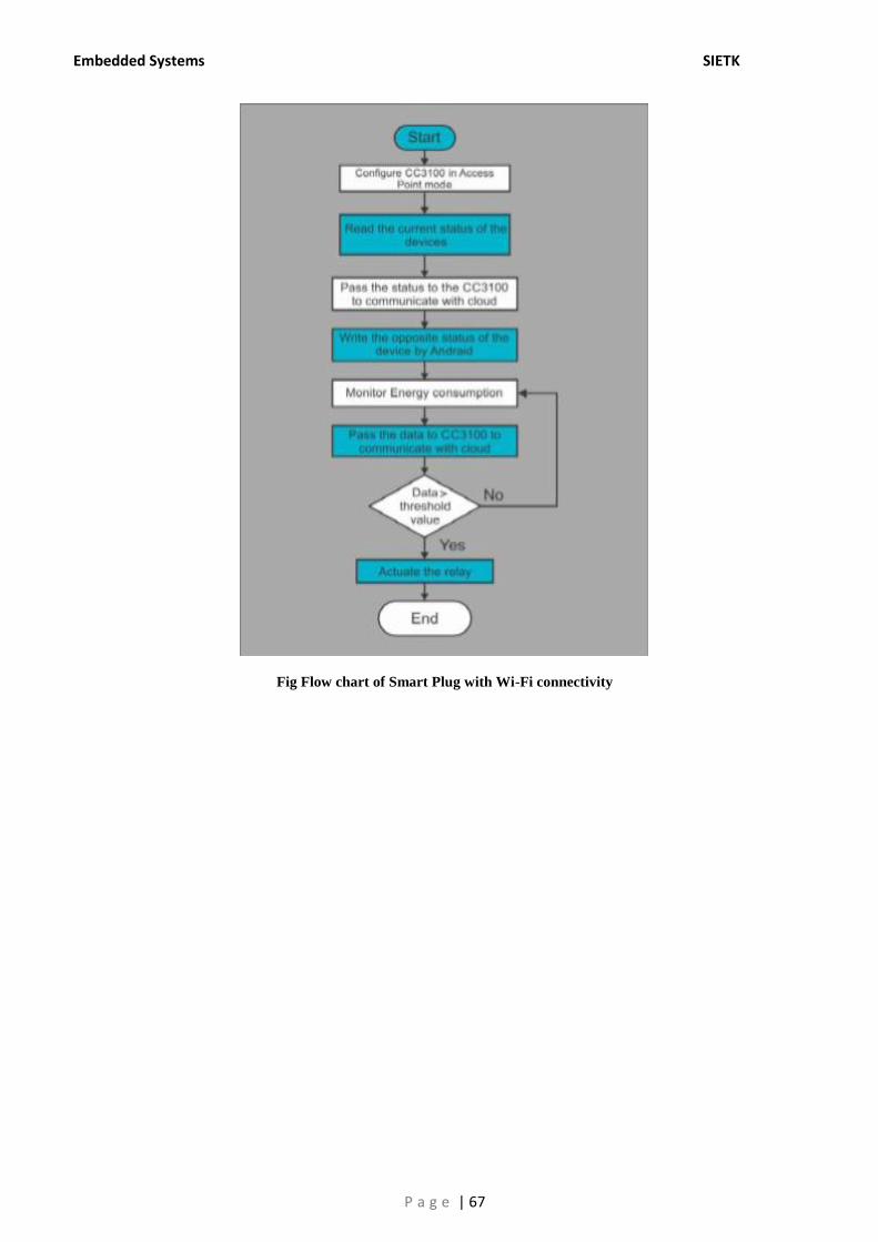
Embedded Systems SIETK
P a g e | 67
Fig Flow chart of Smart Plug with Wi-Fi connectivity