Embed Size (px)
Citation preview
SST26VF064B / SST26VF064BA2.5V/3.0V 64 Mbit Serial Quad I/O (SQI) Flash Memory
Features• Single Voltage Read and Write Operations
- 2.7-3.6V or 2.3-3.6V• Serial Interface Architecture
- Nibble-wide multiplexed I/O’s with SPI-like serial command structure - Mode 0 and Mode 3
- x1/x2/x4 Serial Peripheral Interface (SPI) Protocol• High Speed Clock Frequency
- 2.7-3.6V: 104 MHz max- 2.3-3.6V: 80 MHz max
• Burst Modes- Continuous linear burst- 8/16/32/64 Byte linear burst with wrap-around
• Superior Reliability- Endurance: 100,000 Cycles (min)- Greater than 100 years Data Retention
• Low Power Consumption:- Active Read current: 15 mA (typical @ 104 MHz)- Standby Current: 15 µA (typical)
• Fast Erase Time- Sector/Block Erase: 18 ms (typ), 25ms (max)- Chip Erase: 35 ms (typ), 50 ms (max)
• Page-Program- 256 Bytes per page in x1 or x4 mode
• End-of-Write Detection- Software polling the BUSY bit in status register
• Flexible Erase Capability- Uniform 4 KByte sectors- Four 8 KByte top and bottom parameter
overlay blocks- One 32 KByte top and bottom overlay block- Uniform 64 KByte overlay blocks
• Write-Suspend- Suspend Program or Erase operation to access
another block/sector• Software Reset (RST) mode• Software Protection
- Individual-Block Write Protection with permanent lock-down capability - 64 KByte blocks, two 32 KByte blocks, and eight 8 KByte parameter blocks
- Read Protection on top and bottom 8 KByte parameter blocks
• Security ID- One-Time Programmable (OTP) 2 KByte, Secure ID
- 64 bit unique, factory pre-programmed identifier- User-programmable area
• Temperature Range- Industrial: -40°C to +85°C- Industrial Plus: -40°C to +105°C
• Automotive AECQ-100 Grade 2 and Grade 3• Packages Available
- 8-contact WDFN (6mm x 5mm)- 8-contact WDFN (6mm x 8 mm)- 8-lead SOIJ (5.28 mm)- 16-lead SOIC (7.50 mm)- 24-ball TBGA (6mm x 8mm)
• All devices are RoHS compliant
Product DescriptionThe Serial Quad I/O™ (SQI™) family of flash-memorydevices features a six-wire, 4-bit I/O interface thatallows for low-power, high-performance operation in alow pin-count package. SST26VF064B/064BA alsosupport full command-set compatibility to traditionalSerial Peripheral Interface (SPI) protocol. Systemdesigns using SQI flash devices occupy less boardspace and ultimately lower system costs.All members of the 26 Series, SQI family are manufac-tured with proprietary, high-performance CMOS Super-Flash® technology. The split-gate cell design and thick-oxide tunneling injector attain better reliability and man-ufacturability compared with alternate approaches.SST26VF064B/064BA significantly improve perfor-mance and reliability, while lowering power consump-tion. These devices write (Program or Erase) with asingle power supply of 2.3-3.6V. The total energy con-sumed is a function of the applied voltage, current, andtime of application. Since for any given voltage range,the SuperFlash technology uses less current to pro-gram and has a shorter erase time, the total energyconsumed during any Erase or Program operation isless than alternative flash memory technologies. SST26VF064B/064BA are offered in 8-contact WDFN(6 mm x 5 mm or 6mm x 8mm), 8-lead SOIJ (5.28 mm),16-lead SOIC (7.50 mm), and 24-ball TBGA. See Fig-ure 2-2 for pin assignments.Two configurations are available upon order.SST26VF064B default at power-up has the WP# andHOLD# pins enabled, and the SIO2 and SIO3 pins dis-
2015-2019 Microchip Technology Inc. DS20005119J-page 1
SST26VF064B / SST26VF064BA
abled, to initiate SPI-protocol operations.SST26VF064BA default at power-up has the WP# andHOLD# pins disabled, and the SIO2 and SIO3 pins
enabled, to initiate Quad I/O operations. See “I/O Con-figuration (IOC)” on page 12 for more information aboutconfiguring WP#/HOLD# and SIO3/SIO4 pins.
TO OUR VALUED CUSTOMERSIt is our intention to provide our valued customers with the best documentation possible to ensure successful use of your Microchipproducts. To this end, we will continue to improve our publications to better suit your needs. Our publications will be refined andenhanced as new volumes and updates are introduced. If you have any questions or comments regarding this publication, please contact the Marketing Communications Department viaE-mail at [email protected]. We welcome your feedback.
Most Current Data SheetTo obtain the most up-to-date version of this data sheet, please register at our Worldwide Web site at:
http://www.microchip.comYou can determine the version of a data sheet by examining its literature number found on the bottom outside corner of any page.The last character of the literature number is the version number, (e.g., DS30000000A is version A of document DS30000000).
ErrataAn errata sheet, describing minor operational differences from the data sheet and recommended workarounds, may exist for currentdevices. As device/documentation issues become known to us, we will publish an errata sheet. The errata will specify the revisionof silicon and revision of document to which it applies.To determine if an errata sheet exists for a particular device, please check with one of the following:• Microchip’s Worldwide Web site; http://www.microchip.com• Your local Microchip sales office (see last page)When contacting a sales office, please specify which device, revision of silicon and data sheet (include literature number) you areusing.
Customer Notification SystemRegister on our web site at www.microchip.com to receive the most current information on all of our products.
2015-2019 Microchip Technology Inc. DS20005119J-page 2
SST26VF064B / SST26VF064BA
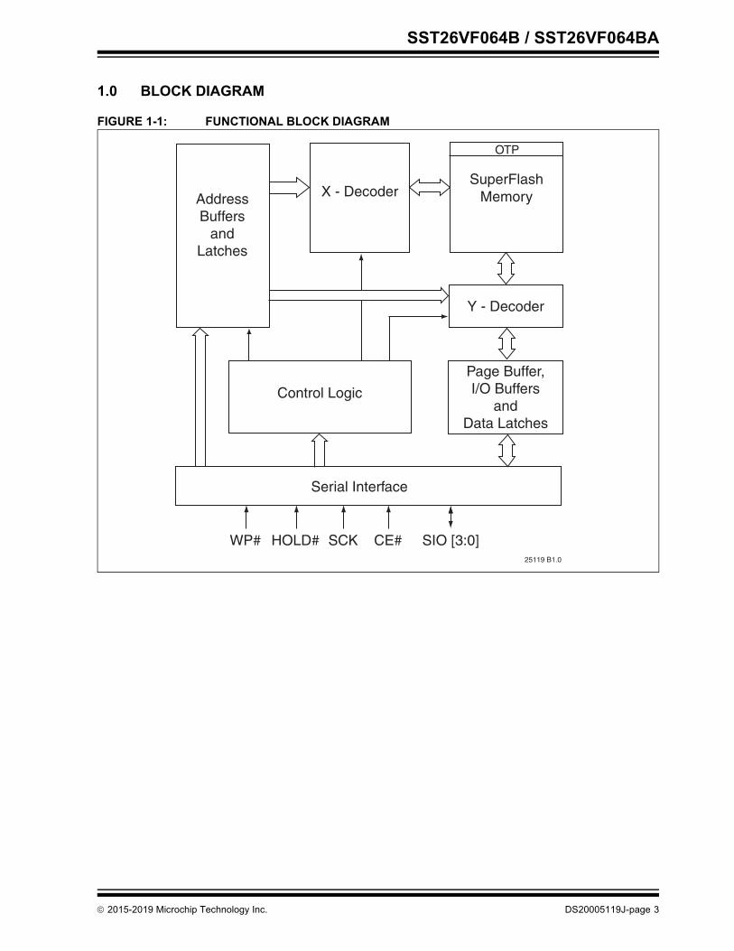
1.0 BLOCK DIAGRAM
FIGURE 1-1: FUNCTIONAL BLOCK DIAGRAM
25119 B1.0
Page Buffer,I/O Buffers
andData Latches
SuperFlashMemoryX - Decoder
Control Logic
AddressBuffers
andLatches
HOLD#
Y - Decoder
CE# SIO [3:0]
Serial Interface
OTP
WP# SCK
2015-2019 Microchip Technology Inc. DS20005119J-page 3
SST26VF064B / SST26VF064BA
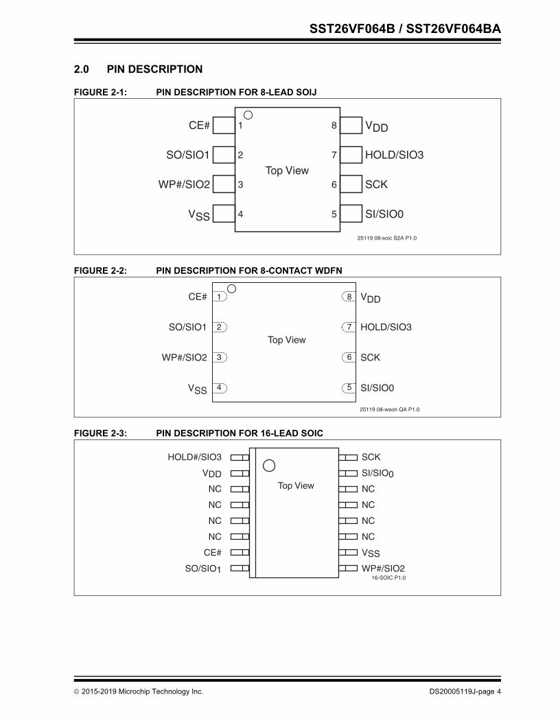
2.0 PIN DESCRIPTION
FIGURE 2-1: PIN DESCRIPTION FOR 8-LEAD SOIJ
FIGURE 2-2: PIN DESCRIPTION FOR 8-CONTACT WDFN
FIGURE 2-3: PIN DESCRIPTION FOR 16-LEAD SOIC
1
2
3
4
8
7
6
5
CE#
SO/SIO1
WP#/SIO2
VSS
VDD
HOLD/SIO3
SCK
SI/SIO0
Top View
25119 08-soic S2A P1.0
1
2
3
4
8
7
6
5
CE#
SO/SIO1
WP#/SIO2
VSS
Top View
VDD
HOLD/SIO3
SCK
SI/SIO0
25119 08-wson QA P1.0
SCK
SI/SIO0
NC
NC
NC
NC
VSS
WP#/SIO2
HOLD#/SIO3
VDD
NC
NC
NC
NC
CE#
SO/SIO116-SOIC P1.0
Top View
2015-2019 Microchip Technology Inc. DS20005119J-page 4
SST26VF064B / SST26VF064BA
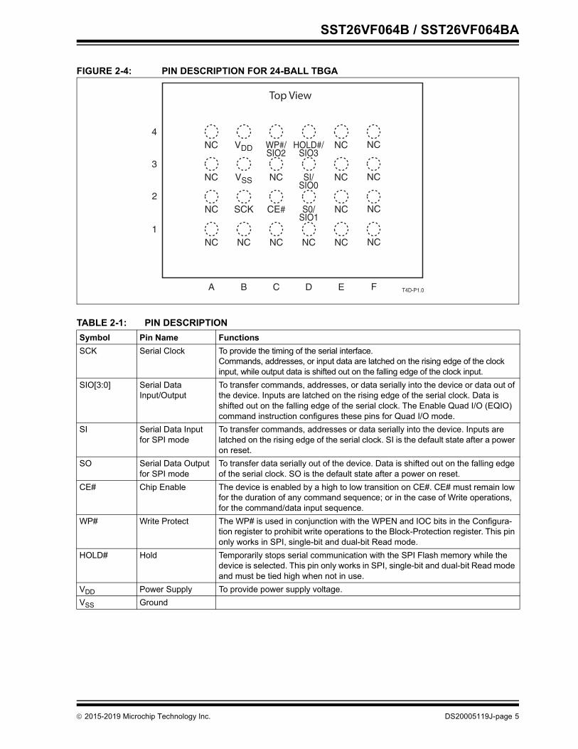
FIGURE 2-4: PIN DESCRIPTION FOR 24-BALL TBGA
TABLE 2-1: PIN DESCRIPTIONSymbol Pin Name FunctionsSCK Serial Clock To provide the timing of the serial interface.
Commands, addresses, or input data are latched on the rising edge of the clock input, while output data is shifted out on the falling edge of the clock input.
SIO[3:0] Serial Data Input/Output
To transfer commands, addresses, or data serially into the device or data out of the device. Inputs are latched on the rising edge of the serial clock. Data is shifted out on the falling edge of the serial clock. The Enable Quad I/O (EQIO) command instruction configures these pins for Quad I/O mode.
SI Serial Data Input for SPI mode
To transfer commands, addresses or data serially into the device. Inputs are latched on the rising edge of the serial clock. SI is the default state after a power on reset.
SO Serial Data Output for SPI mode
To transfer data serially out of the device. Data is shifted out on the falling edge of the serial clock. SO is the default state after a power on reset.
CE# Chip Enable The device is enabled by a high to low transition on CE#. CE# must remain low for the duration of any command sequence; or in the case of Write operations, for the command/data input sequence.
WP# Write Protect The WP# is used in conjunction with the WPEN and IOC bits in the Configura-tion register to prohibit write operations to the Block-Protection register. This pin only works in SPI, single-bit and dual-bit Read mode.
HOLD# Hold Temporarily stops serial communication with the SPI Flash memory while the device is selected. This pin only works in SPI, single-bit and dual-bit Read mode and must be tied high when not in use.
VDD Power Supply To provide power supply voltage.VSS Ground
NC
NC
NC
NC
NC
SCK
VSS
VDD
NC
CE#
NC
WP#/SIO2
NC
S0/SIO1
SI/SIO0
HOLD#/SIO3
NC
NC
NC
NC
NC
NC
NC
NC
A B C D E F
1
2
3
4
T4D-P1.0
Top View
2015-2019 Microchip Technology Inc. DS20005119J-page 5
SST26VF064B / SST26VF064BA
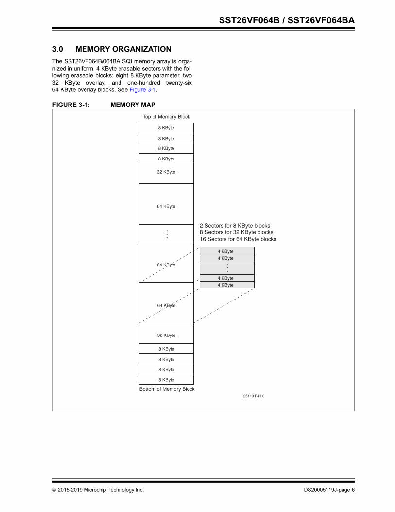
3.0 MEMORY ORGANIZATIONThe SST26VF064B/064BA SQI memory array is orga-nized in uniform, 4 KByte erasable sectors with the fol-lowing erasable blocks: eight 8 KByte parameter, two32 KByte overlay, and one-hundred twenty-six64 KByte overlay blocks. See Figure 3-1.
FIGURE 3-1: MEMORY MAP
25119 F41.0
Top of Memory Block
8 KByte
8 KByte
8 KByte
8 KByte
32 KByte
64 KByte
64 KByte
64 KByte
32 KByte
8 KByte
8 KByte
8 KByte
8 KByte
Bottom of Memory Block
4 KByte
4 KByte
4 KByte
4 KByte
. . .
2 Sectors for 8 KByte blocks8 Sectors for 32 KByte blocks16 Sectors for 64 KByte blocks. .
.
2015-2019 Microchip Technology Inc. DS20005119J-page 6
SST26VF064B / SST26VF064BA
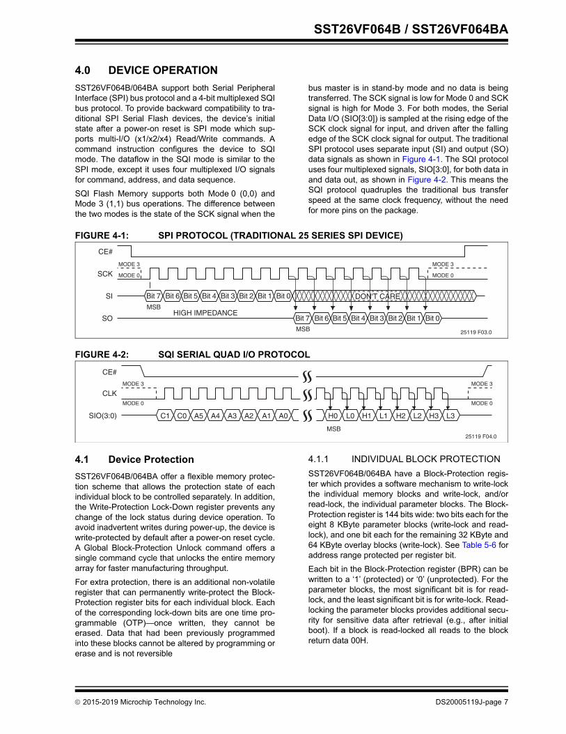
4.0 DEVICE OPERATIONSST26VF064B/064BA support both Serial PeripheralInterface (SPI) bus protocol and a 4-bit multiplexed SQIbus protocol. To provide backward compatibility to tra-ditional SPI Serial Flash devices, the device’s initialstate after a power-on reset is SPI mode which sup-ports multi-I/O (x1/x2/x4) Read/Write commands. Acommand instruction configures the device to SQImode. The dataflow in the SQI mode is similar to theSPI mode, except it uses four multiplexed I/O signalsfor command, address, and data sequence.SQI Flash Memory supports both Mode 0 (0,0) andMode 3 (1,1) bus operations. The difference betweenthe two modes is the state of the SCK signal when the
bus master is in stand-by mode and no data is beingtransferred. The SCK signal is low for Mode 0 and SCKsignal is high for Mode 3. For both modes, the SerialData I/O (SIO[3:0]) is sampled at the rising edge of theSCK clock signal for input, and driven after the fallingedge of the SCK clock signal for output. The traditionalSPI protocol uses separate input (SI) and output (SO)data signals as shown in Figure 4-1. The SQI protocoluses four multiplexed signals, SIO[3:0], for both data inand data out, as shown in Figure 4-2. This means theSQI protocol quadruples the traditional bus transferspeed at the same clock frequency, without the needfor more pins on the package.
FIGURE 4-1: SPI PROTOCOL (TRADITIONAL 25 SERIES SPI DEVICE)
FIGURE 4-2: SQI SERIAL QUAD I/O PROTOCOL
4.1 Device ProtectionSST26VF064B/064BA offer a flexible memory protec-tion scheme that allows the protection state of eachindividual block to be controlled separately. In addition,the Write-Protection Lock-Down register prevents anychange of the lock status during device operation. Toavoid inadvertent writes during power-up, the device iswrite-protected by default after a power-on reset cycle.A Global Block-Protection Unlock command offers asingle command cycle that unlocks the entire memoryarray for faster manufacturing throughput. For extra protection, there is an additional non-volatileregister that can permanently write-protect the Block-Protection register bits for each individual block. Eachof the corresponding lock-down bits are one time pro-grammable (OTP)—once written, they cannot beerased. Data that had been previously programmedinto these blocks cannot be altered by programming orerase and is not reversible
4.1.1 INDIVIDUAL BLOCK PROTECTIONSST26VF064B/064BA have a Block-Protection regis-ter which provides a software mechanism to write-lockthe individual memory blocks and write-lock, and/orread-lock, the individual parameter blocks. The Block-Protection register is 144 bits wide: two bits each for theeight 8 KByte parameter blocks (write-lock and read-lock), and one bit each for the remaining 32 KByte and64 KByte overlay blocks (write-lock). See Table 5-6 foraddress range protected per register bit.Each bit in the Block-Protection register (BPR) can bewritten to a ‘1’ (protected) or ‘0’ (unprotected). For theparameter blocks, the most significant bit is for read-lock, and the least significant bit is for write-lock. Read-locking the parameter blocks provides additional secu-rity for sensitive data after retrieval (e.g., after initialboot). If a block is read-locked all reads to the blockreturn data 00H.
25119 F03.0
MODE 3
SCK
SI
SO
CE#
MODE 3
DON'T CARE
Bit 7 Bit 6 Bit 5 Bit 4 Bit 3 Bit 2 Bit 1 Bit 0
Bit 7 Bit 6 Bit 5 Bit 4 Bit 3 Bit 2 Bit 1 Bit 0
MODE 0MODE 0
HIGH IMPEDANCEMSB
MSB
25119 F04.0
MODE 3
CLK
SIO(3:0)
CE#
MODE 3
C1 C0 A5 A4 A3 A2 A1 A0 H0 L0 H1 L1 H2 L2 H3 L3
MODE 0MODE 0
MSB
2015-2019 Microchip Technology Inc. DS20005119J-page 7
SST26VF064B / SST26VF064BA
The Write Block-Protection Register command is atwo-cycle command which requires that Write-Enable(WREN) is executed prior to the Write Block-ProtectionRegister command. The Global Block-ProtectionUnlock command clears all write protection bits in theBlock-Protection register.
4.1.2 WRITE-PROTECTION LOCK-DOWN (VOLATILE)
To prevent changes to the Block-Protection register,use the Lock-Down Block-Protection Register (LBPR)command to enable Write-Protection Lock-Down.Once Write-Protection Lock-Down is enabled, theBlock-Protection register can not be changed. To avoidinadvertent lock down, the WREN command must beexecuted prior to the LBPR command. To reset Write-Protection Lock-Down, performing a powercycle on the device is required. The Write-ProtectionLock-Down status may be read from the Status register.
4.1.3 WRITE-LOCK LOCK-DOWN (NON-VOLATILE)
The non-Volatile Write-Lock Lock-Down register is analternate register that permanently prevents changesto the block-protect bits. The non-Volatile Write-LockLock-Down register (nVWLDR) is 136 bits wide perdevice: one bit each for the eight 8-KByte parameterblocks, and one bit each for the remaining 32 KByteand 64 KByte overlay blocks. See Table 5-6 for addressrange protected per register bit.Writing ‘1’ to any or all of the nVWLDR bits disables thechange mechanism for the corresponding Write-Lockbit in the BPR, and permanently sets this bit to a ‘1’(protected) state. After this change, both bits will be setto ‘1’, regardless of the data entered in subsequentwrites to either the nVWLDR or the BPR. Subsequentwrites to the nVWLDR can only alter available locationsthat have not been previously written to a ‘1’. Thismethod provides write-protection for the correspondingmemory-array block by protecting it from future pro-gram or erase operations.
Writing a ‘0’ in any location in the nVWLDR has noeffect on either the nVWLDR or the correspondingWrite-Lock bit in the BPR. Note that if the Block-Protection register had been pre-viously locked down, see “Write-Protection Lock-Down(Volatile)”, the device must be power cycled beforeusing the nVWLDR. If the Block-Protection register islocked down and the Write nVWLDR command isaccessed, the command will be ignored.
4.2 Hardware Write ProtectionThe hardware Write Protection pin (WP#) is used inconjunction with the WPEN and IOC bits in the config-uration register to prohibit write operations to the Block-Protection and Configuration registers. The WP# pinfunction only works in SPI single-bit and dual-bit readmode when the IOC bit in the configuration register isset to ‘0’. The WP# pin function is disabled when the WPEN bitin the configuration register is ‘0’. This allows installa-tion of the SST26VF064B/064BA in a system with agrounded WP# pin while still enabling Write to theBlock-Protection register. The Lock-Down function ofthe Block-Protection Register supersedes the WP# pin,see Table 4-1 for Write Protection Lock-Down states. The factory default setting at power-up of the WPEN bitis ‘0’, disabling the Write Protect function of the WP#after power-up. WPEN is a non-volatile bit; once the bitis set to ‘1’, the Write Protect function of the WP# pincontinues to be enabled after power-up. The WP# pinonly protects the Block-Protection Register and Config-uration Register from changes. Therefore, if the WP#pin is set to low before or after a Program or Erasecommand, or while an internal Write is in progress, itwill have no effect on the Write command. The IOC bit takes priority over the WPEN bit in the con-figuration register. When the IOC bit is ‘1’, the functionof the WP# pin is disabled and the WPEN bit serves nofunction. When the IOC bit is ‘0’ and WPEN is ‘1’, set-ting the WP# pin active low prohibits Write operationsto the Block Protection Register.
2015-2019 Microchip Technology Inc. DS20005119J-page 8
SST26VF064B / SST26VF064BA
4.3 Security IDSST26VF064B/064BA offer a 2 KByte Security ID (SecID) feature. The Security ID space is divided into twoparts – one factory-programmed, 64-bit segment andone user-programmable segment. The factory-pro-grammed segment is programmed during manufactur-ing with a unique number and cannot be changed. Theuser-programmable segment is left unprogrammed forthe customer to program as desired.Use the Program Security ID (PSID) command to pro-gram the Security ID using the address shown in Table5-5. The Security ID can be locked using the LockoutSecurity ID (LSID) command. This prevents any futurewrite operations to the Security ID. The factory-programmed portion of the Security IDcan’t be programmed by the user; neither the factory-programmed nor user-programmable areas can beerased.
4.4 Hold OperationThe HOLD# pin pauses active serial sequences with-out resetting the clocking sequence. This pin is activeafter every power up and only operates during SPIsingle-bit and dual-bit modes. Two factory configura-tions are available: SST26VF064B ships with the IOC
bit set to ‘0’ and the HOLD# pin function enabled;SST26VF064BA ships with the IOC bit set to ‘1’ and theHOLD# pin function disabled. The HOLD# pin is alwaysdisabled in SQI mode and only works in SPI single-bitand dual-bit read mode.To activate the Hold mode, CE# must be in active lowstate. The Hold mode begins when the SCK active lowstate coincides with the falling edge of the HOLD# sig-nal. The Hold mode ends when the HOLD# signal’s ris-ing edge coincides with the SCK active low state. If the falling edge of the HOLD# signal does not coin-cide with the SCK active low state, then the deviceenters Hold mode when the SCK next reaches theactive low state. Similarly, if the rising edge of theHOLD# signal does not coincide with the SCK activelow state, then the device exits Hold mode when theSCK next reaches the active low state. See Figure 4-3.Once the device enters Hold mode, SO will be in highimpedance state while SI and SCK can be VIL or VIH.If CE# is driven active high during a Hold condition, itresets the internal logic of the device. As long asHOLD# signal is low, the memory remains in the Holdcondition. To resume communication with the device,HOLD# must be driven active high, and CE# must bedriven active low.
FIGURE 4-3: HOLD CONDITION WAVEFORM.
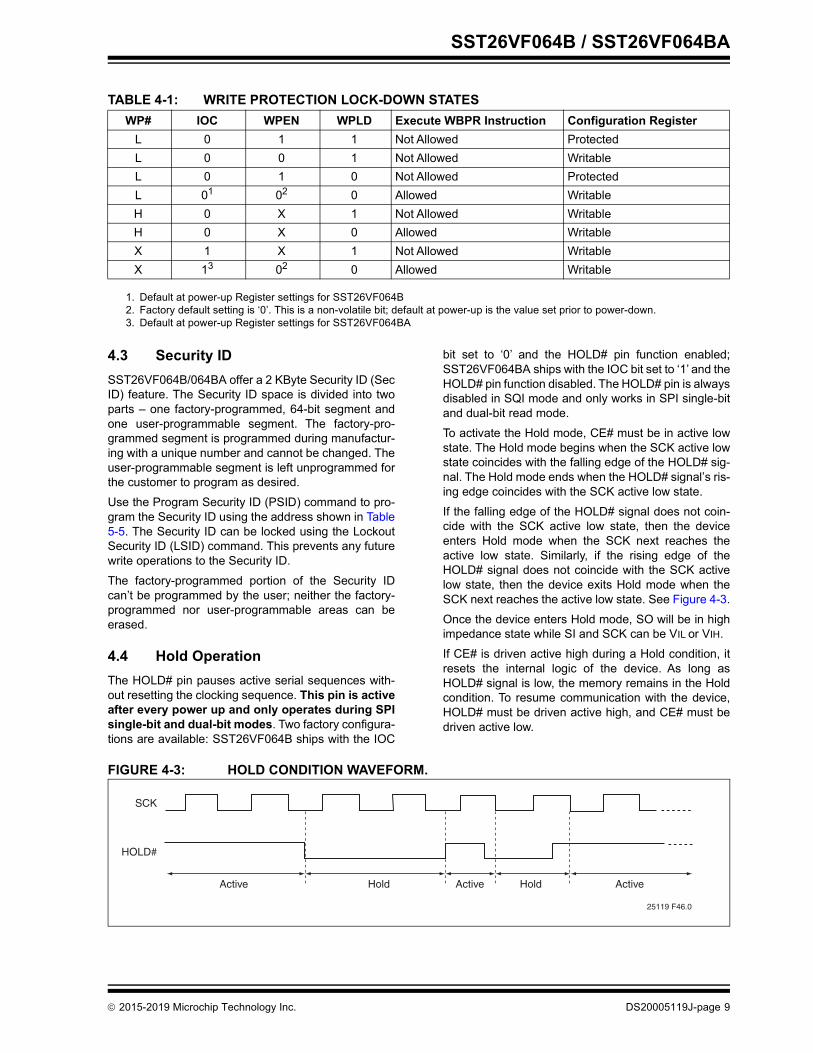
TABLE 4-1: WRITE PROTECTION LOCK-DOWN STATESWP# IOC WPEN WPLD Execute WBPR Instruction Configuration Register
L 0 1 1 Not Allowed ProtectedL 0 0 1 Not Allowed WritableL 0 1 0 Not Allowed ProtectedL 01 02 0 Allowed WritableH 0 X 1 Not Allowed WritableH 0 X 0 Allowed WritableX 1 X 1 Not Allowed WritableX 13 02 0 Allowed Writable
1. Default at power-up Register settings for SST26VF064B2. Factory default setting is ‘0’. This is a non-volatile bit; default at power-up is the value set prior to power-down.3. Default at power-up Register settings for SST26VF064BA
Active Hold Active Hold Active
25119 F46.0
SCK
HOLD#
2015-2019 Microchip Technology Inc. DS20005119J-page 9
SST26VF064B / SST26VF064BA
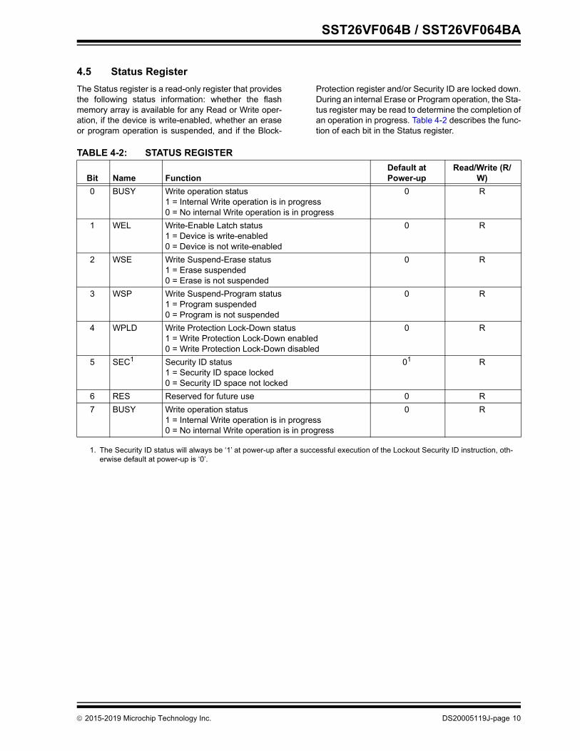
4.5 Status RegisterThe Status register is a read-only register that providesthe following status information: whether the flashmemory array is available for any Read or Write oper-ation, if the device is write-enabled, whether an eraseor program operation is suspended, and if the Block-
Protection register and/or Security ID are locked down.During an internal Erase or Program operation, the Sta-tus register may be read to determine the completion ofan operation in progress. Table 4-2 describes the func-tion of each bit in the Status register.
TABLE 4-2: STATUS REGISTER
Bit Name FunctionDefault atPower-up
Read/Write (R/W)
0 BUSY Write operation status1 = Internal Write operation is in progress0 = No internal Write operation is in progress
0 R
1 WEL Write-Enable Latch status1 = Device is write-enabled0 = Device is not write-enabled
0 R
2 WSE Write Suspend-Erase status1 = Erase suspended0 = Erase is not suspended
0 R
3 WSP Write Suspend-Program status1 = Program suspended0 = Program is not suspended
0 R
4 WPLD Write Protection Lock-Down status1 = Write Protection Lock-Down enabled0 = Write Protection Lock-Down disabled
0 R
5 SEC1
1. The Security ID status will always be ‘1’ at power-up after a successful execution of the Lockout Security ID instruction, oth-erwise default at power-up is ‘0’.
Security ID status1 = Security ID space locked0 = Security ID space not locked
01 R
6 RES Reserved for future use 0 R7 BUSY Write operation status
1 = Internal Write operation is in progress0 = No internal Write operation is in progress
0 R
2015-2019 Microchip Technology Inc. DS20005119J-page 10
SST26VF064B / SST26VF064BA
4.5.1 WRITE-ENABLE LATCH (WEL)The Write-Enable Latch (WEL) bit indicates the statusof the internal memory’s Write-Enable Latch. If theWEL bit is set to ‘1’, the device is write enabled. If thebit is set to ‘0’ (reset), the device is not write enabledand does not accept any memory Program or Erase,Protection Register Write, or Lock-Down commands.The Write-Enable Latch bit is automatically reset underthe following conditions:• Power-up• Reset• Write-Disable (WRDI) instruction • Page-Program instruction completion• Sector-Erase instruction completion• Block-Erase instruction completion• Chip-Erase instruction completion• Write-Block-Protection register instruction• Lock-Down Block-Protection register instruction• Program Security ID instruction completion• Lockout Security ID instruction completion• Write-Suspend instruction• SPI Quad Page program instruction completion• Write Status Register
4.5.2 WRITE SUSPEND ERASE STATUS (WSE)
The Write Suspend-Erase status (WSE) indicateswhen an Erase operation has been suspended. TheWSE bit is ‘1’ after the host issues a suspend commandduring an Erase operation. Once the suspended Eraseresumes, the WSE bit is reset to ‘0’.
4.5.3 WRITE SUSPEND PROGRAM STATUS (WSP)
The Write Suspend-Program status (WSP) bit indicateswhen a Program operation has been suspended. TheWSP is ‘1’ after the host issues a suspend commandduring the Program operation. Once the suspendedProgram resumes, the WSP bit is reset to ‘0’.
4.5.4 WRITE PROTECTION LOCK-DOWN STATUS (WPLD)
The Write Protection Lock-Down status (WPLD) bitindicates when the Block-Protection register is locked-down to prevent changes to the protection settings.The WPLD is ‘1’ after the host issues a Lock-DownBlock-Protection command. After a power cycle, theWPLD bit is reset to ‘0’.
4.5.5 SECURITY ID STATUS (SEC)The Security ID Status (SEC) bit indicates when theSecurity ID space is locked to prevent a Write com-mand. The SEC is ‘1’ after the host issues a LockoutSID command. Once the host issues a Lockout SIDcommand, the SEC bit can never be reset to ‘0.’
4.5.6 BUSYThe Busy bit determines whether there is an internalErase or Program operation in progress. If the BUSYbit is ‘1’, the device is busy with an internal Erase orProgram operation. If the bit is ‘0’, no Erase or Programoperation is in progress.
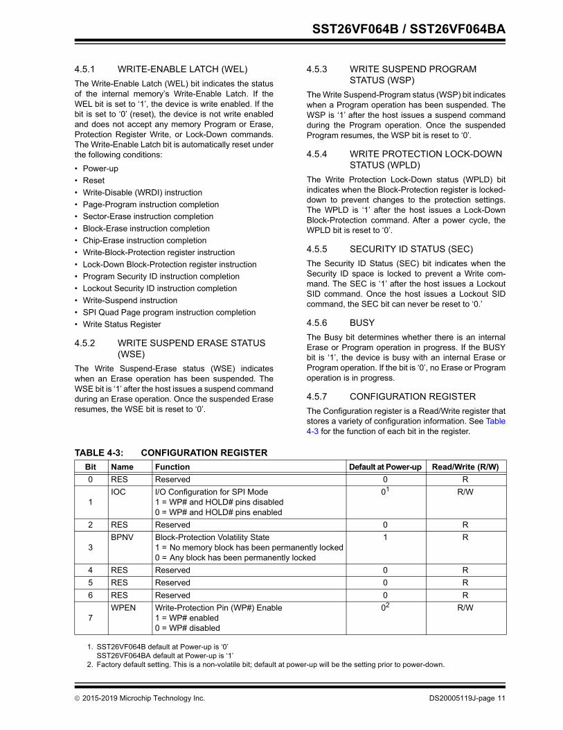
4.5.7 CONFIGURATION REGISTERThe Configuration register is a Read/Write register thatstores a variety of configuration information. See Table4-3 for the function of each bit in the register.
TABLE 4-3: CONFIGURATION REGISTERBit Name Function Default at Power-up Read/Write (R/W)0 RES Reserved 0 R
1IOC I/O Configuration for SPI Mode
1 = WP# and HOLD# pins disabled0 = WP# and HOLD# pins enabled
01
1. SST26VF064B default at Power-up is ‘0’SST26VF064BA default at Power-up is ‘1’
R/W
2 RES Reserved 0 R
3BPNV Block-Protection Volatility State
1 = No memory block has been permanently locked0 = Any block has been permanently locked
1 R
4 RES Reserved 0 R5 RES Reserved 0 R6 RES Reserved 0 R
7WPEN Write-Protection Pin (WP#) Enable
1 = WP# enabled0 = WP# disabled
02
2. Factory default setting. This is a non-volatile bit; default at power-up will be the setting prior to power-down.
R/W
2015-2019 Microchip Technology Inc. DS20005119J-page 11
SST26VF064B / SST26VF064BA
4.5.8 I/O CONFIGURATION (IOC)The I/O Configuration (IOC) bit re-configures the I/Opins. The IOC bit is set by writing a ‘1’ to Bit 1 of theConfiguration register. When IOC bit is ‘0’ the WP# pinand HOLD# pin are enabled (SPI or Dual Configurationsetup). When IOC bit is set to ‘1’ the SIO2 pin and SIO3pin are enabled (SPI Quad I/O Configuration setup).The IOC bit must be set to ‘1’ before issuing the follow-ing SPI commands: SQOR (6BH), SQIOR (EBH),RBSPI (ECH), and SPI Quad page program (32H).Without setting the IOC bit to ‘1’, those SPI commandsare not valid. The I/O configuration bit does not applywhen in SQI mode. The default at power-up forSST26VF064B is ‘0’ and for SST26VF064BA is ‘1’.
4.5.9 BLOCK-PROTECTION VOLATILITY STATE (BPNV)
The Block-Protection Volatility State bit indicateswhether any block has been permanently locked withthe nVWLDR. When no bits in the nVWLDR have beenset, the BPNV is ‘1’; this is the default state from thefactory. When one or more bits in the nVWLDR are setto ‘1’, the BPNV bit will also be ‘0’ from that point for-ward, even after power-up.
4.5.10 WRITE-PROTECT ENABLE (WPEN)The Write-Protect Enable (WPEN) bit is a non-volatilebit that enables the WP# pin.The Write-Protect (WP#) pin and the Write-ProtectEnable (WPEN) bit control the programmable hard-ware write-protect feature. Setting the WP# pin to low,and the WPEN bit to ‘1’, enables Hardware write-pro-tection. To disable Hardware write protection, set eitherthe WP# pin to high or the WPEN bit to ‘0’. There islatency associated with writing to the WPEN bit. Pollthe BUSY bit in the Status register, or wait TWPEN, forthe completion of the internal, self-timed Write opera-tion. When the chip is hardware write protected, onlyWrite operations to Block-Protection and Configurationregisters are disabled. See “Hardware Write Protec-tion” on page 8 and Table 4-1 on page 9 for more infor-mation about the functionality of the WPEN bit.
2015-2019 Microchip Technology Inc. DS20005119J-page 12
SST26VF064B / SST26VF064BA
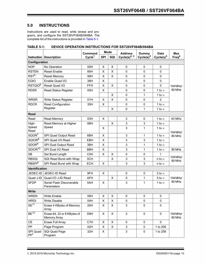
5.0 INSTRUCTIONSInstructions are used to read, write (erase and pro-gram), and configure the SST26VF064B/064BA. Thecomplete list of the instructions is provided in Table 5-1.
TABLE 5-1: DEVICE OPERATION INSTRUCTIONS FOR SST26VF064B/064BA
Instruction DescriptionCommand
Cycle1Mode Address
Cycle(s)2, 3Dummy
Cycle(s)3Data
Cycle(s)3Max
Freq4SPI SQIConfigurationNOP No Operation 00H X X 0 0 0
104 MHz/ 80 MHz
RSTEN Reset Enable 66H X X 0 0 0RST5 Reset Memory 99H X X 0 0 0EQIO Enable Quad I/O 38H X 0 0 0RSTQIO6 Reset Quad I/O FFH X X 0 0 0RDSR Read Status Register 05H X 0 0 1 to
X 0 1 1 to WRSR Write Status Register 01H X X 0 0 2RDCR Read Configuration
Register35H X 0 0 1 to
X 0 1 1 to ReadRead Read Memory 03H X 3 0 1 to 40 MHzHigh-Speed Read
Read Memory at Higher Speed
0BH X 3 3 1 to
104 MHz/ 80 MHz
X 3 1 1 to
SQOR7 SPI Quad Output Read 6BH X 3 1 1 to SQIOR8 SPI Quad I/O Read EBH X 3 3 1 to SDOR9 SPI Dual Output Read 3BH X 3 1 1 to SDIOR10 SPI Dual I/O Read BBH X 3 1 1 to 80 MHzSB Set Burst Length C0H X X 0 0 1
104 MHz/ 80 MHzRBSQI SQI Read Burst with Wrap 0CH X 3 3 n to
RBSPI8 SPI Read Burst with Wrap ECH X 3 3 n to IdentificationJEDEC-ID JEDEC-ID Read 9FH X 0 0 3 to
104 MHz/ 80 MHz
Quad J-ID Quad I/O J-ID Read AFH X 0 1 3 to SFDP Serial Flash Discoverable
Parameters5AH X 3 1 1 to
WriteWREN Write Enable 06H X X 0 0 0
104 MHz/ 80 MHz
WRDI Write Disable 04H X X 0 0 0SE11 Erase 4 KBytes of Memory
Array20H X X 3 0 0
BE12 Erase 64, 32 or 8 KBytes of Memory Array
D8H X X 3 0 0
CE Erase Full Array C7H X X 0 0 0PP Page Program 02H X X 3 0 1 to 256SPI Quad PP7
SQI Quad Page Program
32H X 3 0 1 to 256
2015-2019 Microchip Technology Inc. DS20005119J-page 13
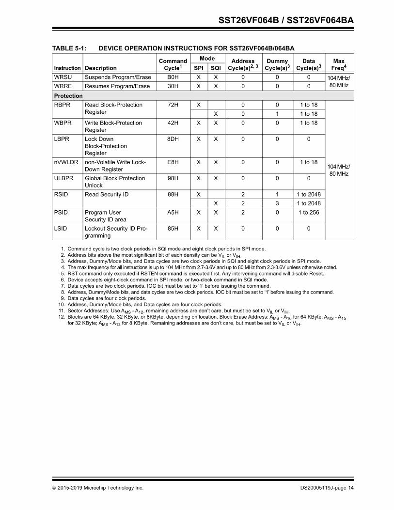
SST26VF064B / SST26VF064BA
WRSU Suspends Program/Erase B0H X X 0 0 0 104 MHz/ 80 MHzWRRE Resumes Program/Erase 30H X X 0 0 0
ProtectionRBPR Read Block-Protection
Register72H X 0 0 1 to18
104 MHz/ 80 MHz
X 0 1 1 to18WBPR Write Block-Protection
Register42H X X 0 0 1 to 18
LBPR Lock Down Block-ProtectionRegister
8DH X X 0 0 0
nVWLDR non-Volatile Write Lock-Down Register
E8H X X 0 0 1 to 18
ULBPR Global Block Protection Unlock
98H X X 0 0 0
RSID Read Security ID 88H X 2 1 1 to 2048X 2 3 1 to 2048
PSID Program User Security ID area
A5H X X 2 0 1 to 256
LSID Lockout Security ID Pro-gramming
85H X X 0 0 0
1. Command cycle is two clock periods in SQI mode and eight clock periods in SPI mode.2. Address bits above the most significant bit of each density can be VIL or VIH.3. Address, Dummy/Mode bits, and Data cycles are two clock periods in SQI and eight clock periods in SPI mode.4. The max frequency for all instructions is up to 104 MHz from 2.7-3.6V and up to 80 MHz from 2.3-3.6V unless otherwise noted.5. RST command only executed if RSTEN command is executed first. Any intervening command will disable Reset.6. Device accepts eight-clock command in SPI mode, or two-clock command in SQI mode.7. Data cycles are two clock periods. IOC bit must be set to ‘1’ before issuing the command.8. Address, Dummy/Mode bits, and data cycles are two clock periods. IOC bit must be set to ‘1’ before issuing the command.9. Data cycles are four clock periods.
10. Address, Dummy/Mode bits, and Data cycles are four clock periods.11. Sector Addresses: Use AMS - A12, remaining address are don’t care, but must be set to VIL or VIH.12. Blocks are 64 KByte, 32 KByte, or 8KByte, depending on location. Block Erase Address: AMS - A16 for 64 KByte; AMS - A15
for 32 KByte; AMS - A13 for 8 KByte. Remaining addresses are don’t care, but must be set to VIL or VIH.
TABLE 5-1: DEVICE OPERATION INSTRUCTIONS FOR SST26VF064B/064BA
Instruction DescriptionCommand
Cycle1Mode Address
Cycle(s)2, 3Dummy
Cycle(s)3Data
Cycle(s)3Max
Freq4SPI SQI
2015-2019 Microchip Technology Inc. DS20005119J-page 14
SST26VF064B / SST26VF064BA
5.1 No Operation (NOP)The No Operation command only cancels a ResetEnable command. NOP has no impact on any othercommand.
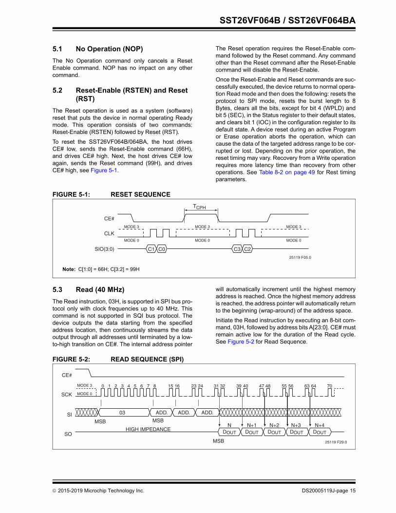
5.2 Reset-Enable (RSTEN) and Reset (RST)
The Reset operation is used as a system (software)reset that puts the device in normal operating Readymode. This operation consists of two commands:Reset-Enable (RSTEN) followed by Reset (RST).To reset the SST26VF064B/064BA, the host drivesCE# low, sends the Reset-Enable command (66H),and drives CE# high. Next, the host drives CE# lowagain, sends the Reset command (99H), and drivesCE# high, see Figure 5-1.
The Reset operation requires the Reset-Enable com-mand followed by the Reset command. Any commandother than the Reset command after the Reset-Enablecommand will disable the Reset-Enable.Once the Reset-Enable and Reset commands are suc-cessfully executed, the device returns to normal opera-tion Read mode and then does the following: resets theprotocol to SPI mode, resets the burst length to 8Bytes, clears all the bits, except for bit 4 (WPLD) andbit 5 (SEC), in the Status register to their default states,and clears bit 1 (IOC) in the configuration register to itsdefault state. A device reset during an active Programor Erase operation aborts the operation, which cancause the data of the targeted address range to be cor-rupted or lost. Depending on the prior operation, thereset timing may vary. Recovery from a Write operationrequires more latency time than recovery from otheroperations. See Table 8-2 on page 49 for Rest timingparameters.
FIGURE 5-1: RESET SEQUENCE
5.3 Read (40 MHz)The Read instruction, 03H, is supported in SPI bus pro-tocol only with clock frequencies up to 40 MHz. Thiscommand is not supported in SQI bus protocol. Thedevice outputs the data starting from the specifiedaddress location, then continuously streams the dataoutput through all addresses until terminated by a low-to-high transition on CE#. The internal address pointer
will automatically increment until the highest memoryaddress is reached. Once the highest memory addressis reached, the address pointer will automatically returnto the beginning (wrap-around) of the address space. Initiate the Read instruction by executing an 8-bit com-mand, 03H, followed by address bits A[23:0]. CE# mustremain active low for the duration of the Read cycle.See Figure 5-2 for Read Sequence.
FIGURE 5-2: READ SEQUENCE (SPI)
25119 F05.0
MODE 3
CLK
SIO(3:0)
CE#
MODE 3
C1 C3 C2C0
MODE 0
MODE 3
MODE 0MODE 0
TCPH
Note: C[1:0] = 66H; C[3:2] = 99H
25119 F29.0
CE#
SO
SI
SCK
ADD.
0 1 2 3 4 5 6 7 8
ADD. ADD.03
HIGH IMPEDANCE
15 16 23 24 31 32 39 40 7047 48 55 56 63 64
N+2 N+3 N+4N N+1DOUT
MSB MSB
MSB
MODE 0
MODE 3
DOUT DOUT DOUT DOUT
2015-2019 Microchip Technology Inc. DS20005119J-page 15
SST26VF064B / SST26VF064BA
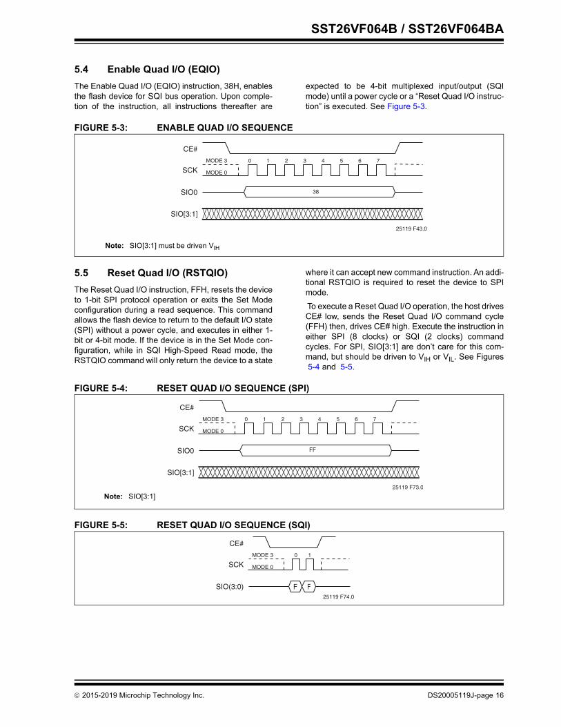
5.4 Enable Quad I/O (EQIO)The Enable Quad I/O (EQIO) instruction, 38H, enablesthe flash device for SQI bus operation. Upon comple-tion of the instruction, all instructions thereafter are
expected to be 4-bit multiplexed input/output (SQImode) until a power cycle or a “Reset Quad I/O instruc-tion” is executed. See Figure 5-3.
FIGURE 5-3: ENABLE QUAD I/O SEQUENCE
5.5 Reset Quad I/O (RSTQIO)The Reset Quad I/O instruction, FFH, resets the deviceto 1-bit SPI protocol operation or exits the Set Modeconfiguration during a read sequence. This commandallows the flash device to return to the default I/O state(SPI) without a power cycle, and executes in either 1-bit or 4-bit mode. If the device is in the Set Mode con-figuration, while in SQI High-Speed Read mode, theRSTQIO command will only return the device to a state
where it can accept new command instruction. An addi-tional RSTQIO is required to reset the device to SPImode. To execute a Reset Quad I/O operation, the host drivesCE# low, sends the Reset Quad I/O command cycle(FFH) then, drives CE# high. Execute the instruction ineither SPI (8 clocks) or SQI (2 clocks) commandcycles. For SPI, SIO[3:1] are don’t care for this com-mand, but should be driven to VIH or VIL. See Figures5-4 and 5-5.
FIGURE 5-4: RESET QUAD I/O SEQUENCE (SPI)
FIGURE 5-5: RESET QUAD I/O SEQUENCE (SQI)
25119 F43.0
MODE 3 0 1
SCK
SIO0
CE#
MODE 0
2 3 4 5 6 7
38
SIO[3:1]
Note: SIO[3:1] must be driven VIH
25119 F73.0
MODE 3 0 1
SCK
SIO0
CE#
MODE 0
2 3 4 5 6 7
FF
SIO[3:1]
Note: SIO[3:1]
25119 F74.0
MODE 3 0 1
SCK
SIO(3:0)
CE#
F F
MODE 0
2015-2019 Microchip Technology Inc. DS20005119J-page 16
SST26VF064B / SST26VF064BA
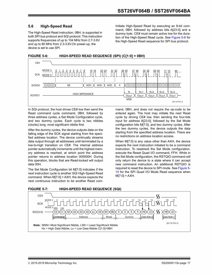
5.6 High-Speed ReadThe High-Speed Read instruction, 0BH, is supported in both SPI bus protocol and SQI protocol. This instruction supports frequencies of up to 104 MHz from 2.7-3.6V and up to 80 MHz from 2.3-3.6V.On power-up, the device is set to use SPI.
Initiate High-Speed Read by executing an 8-bit com-mand, 0BH, followed by address bits A[23-0] and adummy byte. CE# must remain active low for the dura-tion of the High-Speed Read cycle. See Figure 5-6 forthe High-Speed Read sequence for SPI bus protocol.
FIGURE 5-6: HIGH-SPEED READ SEQUENCE (SPI) (C[1:0] = 0BH)
In SQI protocol, the host drives CE# low then send theRead command cycle command, 0BH, followed bythree address cycles, a Set Mode Configuration cycle,and two dummy cycles. Each cycle is two nibbles(clocks) long, most significant nibble first. After the dummy cycles, the device outputs data on thefalling edge of the SCK signal starting from the speci-fied address location. The device continually streamsdata output through all addresses until terminated by alow-to-high transition on CE#. The internal addresspointer automatically increments until the highest mem-ory address is reached, at which point the addresspointer returns to address location 000000H. Duringthis operation, blocks that are Read-locked will outputdata 00H.The Set Mode Configuration bit M[7:0] indicates if thenext instruction cycle is another SQI High-Speed Readcommand. When M[7:0] = AXH, the device expects thenext continuous instruction to be another Read com-
mand, 0BH, and does not require the op-code to beentered again. The host may initiate the next Readcycle by driving CE# low, then sending the four-bitsinput for address A[23:0], followed by the Set Modeconfiguration bits M[7:0], and two dummy cycles. Afterthe two dummy cycles, the device outputs the datastarting from the specified address location. There areno restrictions on address location access. When M[7:0] is any value other than AXH, the deviceexpects the next instruction initiated to be a commandinstruction. To reset/exit the Set Mode configuration,execute the Reset Quad I/O command, FFH. While inthe Set Mode configuration, the RSTQIO command willonly return the device to a state where it can acceptnew command instruction. An additional RSTQIO isrequired to reset the device to SPI mode. See Figure 5-10 for the SPI Quad I/O Mode Read sequence whenM[7:0] = AXH.
FIGURE 5-7: HIGH-SPEED READ SEQUENCE (SQI)
25119 F31.0
CE#
SO/SIO1
SI/SIO0
SCK
ADD.
0 1 2 3 4 5 6 7 8
ADD. ADD.0B
HIGH IMPEDANCE
15 16 23 24 31 32 39 40 47 48 55 56 63 64
N+2 N+3 N+4N N+1
X
MSB
MODE 0
MODE 3
DOUT DOUT DOUT DOUT
8071 72
DOUT
Address DummyCommandCommand Data Byte 0
MSN LSN
Data Byte 7Mode
25119 F47.0
0 1 2
SCK
SIO(3:0)
CE#
C1C0 A5 A4 A3 A2 A1 A0 X H0XXX L0 H8 L8
7 8 11109 1312 1514 2120MODE 3
MODE 0
3 4 5 6
M1 M0
Note: MSN= Most Significant Nibble, LSN = Least Significant NibbleHx = High Data Nibble, Lx = Low Data Nibble C[1:0]=0BH
2015-2019 Microchip Technology Inc. DS20005119J-page 17
SST26VF064B / SST26VF064BA
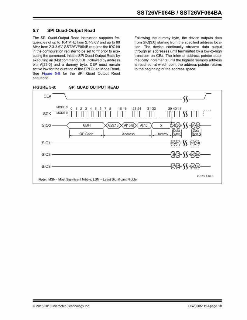
5.7 SPI Quad-Output ReadThe SPI Quad-Output Read instruction supports fre-quencies of up to 104 MHz from 2.7-3.6V and up to 80MHz from 2.3-3.6V. SST26VF064B requires the IOC bitin the configuration register to be set to ‘1’ prior to exe-cuting the command. Initiate SPI Quad-Output Read byexecuting an 8-bit command, 6BH, followed by addressbits A[23-0] and a dummy byte. CE# must remainactive low for the duration of the SPI Quad Mode Read.See Figure 5-8 for the SPI Quad Output Readsequence.
Following the dummy byte, the device outputs datafrom SIO[3:0] starting from the specified address loca-tion. The device continually streams data outputthrough all addresses until terminated by a low-to-hightransition on CE#. The internal address pointer auto-matically increments until the highest memory addressis reached, at which point the address pointer returnsto the beginning of the address space.
FIGURE 5-8: SPI QUAD OUTPUT READ
CE#
SIO0
SCK0 1 2 3 4 5 6 7 8 31 3224MODE 3
MODE 015 16 23
6BH
25119 F48.3
39 40 41
A[23:16] A[15:8] A[7:0] b4 b0 b4 b0
b5 b1 b5 b1
b6 b2 b6 b2
b7 b3 b7 b3
SIO1
SIO2
SIO3
AddressOP CodeData Byte 0Dummy
Data Byte N
X
Note: MSN= Most Significant Nibble, LSN = Least Significant Nibble
2015-2019 Microchip Technology Inc. DS20005119J-page 18
SST26VF064B / SST26VF064BA
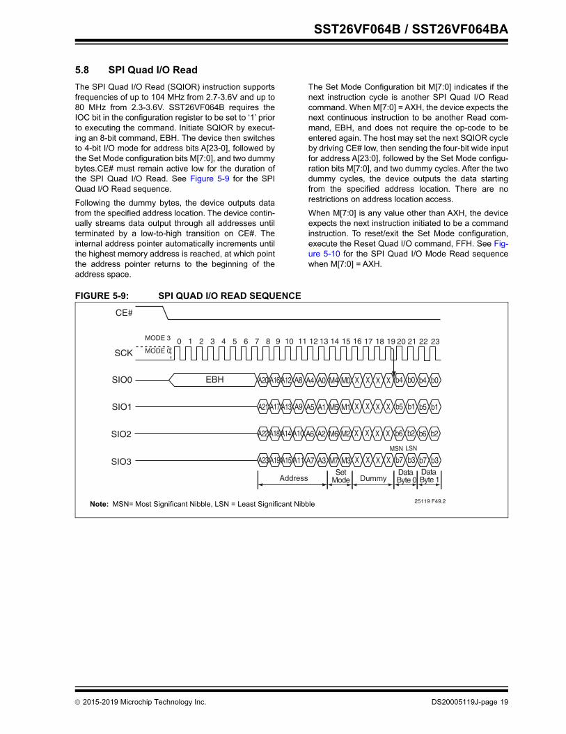
5.8 SPI Quad I/O ReadThe SPI Quad I/O Read (SQIOR) instruction supportsfrequencies of up to 104 MHz from 2.7-3.6V and up to80 MHz from 2.3-3.6V. SST26VF064B requires theIOC bit in the configuration register to be set to ‘1’ priorto executing the command. Initiate SQIOR by execut-ing an 8-bit command, EBH. The device then switchesto 4-bit I/O mode for address bits A[23-0], followed bythe Set Mode configuration bits M[7:0], and two dummybytes.CE# must remain active low for the duration ofthe SPI Quad I/O Read. See Figure 5-9 for the SPIQuad I/O Read sequence.Following the dummy bytes, the device outputs datafrom the specified address location. The device contin-ually streams data output through all addresses untilterminated by a low-to-high transition on CE#. Theinternal address pointer automatically increments untilthe highest memory address is reached, at which pointthe address pointer returns to the beginning of theaddress space.
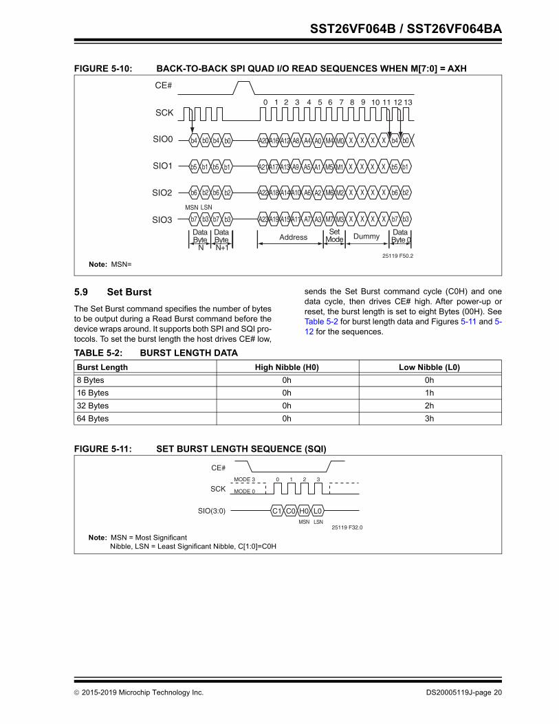
The Set Mode Configuration bit M[7:0] indicates if thenext instruction cycle is another SPI Quad I/O Readcommand. When M[7:0] = AXH, the device expects thenext continuous instruction to be another Read com-mand, EBH, and does not require the op-code to beentered again. The host may set the next SQIOR cycleby driving CE# low, then sending the four-bit wide inputfor address A[23:0], followed by the Set Mode configu-ration bits M[7:0], and two dummy cycles. After the twodummy cycles, the device outputs the data startingfrom the specified address location. There are norestrictions on address location access. When M[7:0] is any value other than AXH, the deviceexpects the next instruction initiated to be a commandinstruction. To reset/exit the Set Mode configuration,execute the Reset Quad I/O command, FFH. See Fig-ure 5-10 for the SPI Quad I/O Mode Read sequencewhen M[7:0] = AXH.
FIGURE 5-9: SPI QUAD I/O READ SEQUENCE
A20 A16 A12 A8 A4 A0 M4 M0
CE#
SIO0
SCK0 1 2 3 4 5 6 7 8 16 1712MODE 3
MODE 09 10 11
EBH
25119 F49.2
b4 b0
SIO1
SIO2
SIO3
AddressData Byte 0Dummy
1513 14 231918 2220 21
b4 b0
A21 A17 A13 A9 A5 A1 M5 M1 b5 b1 b5 b1
A22 A18 A14 A10 A6 A2 M6 M2 b6 b2 b6 b2
A23 A19 A15 A11 A7 A3 M7 M3 b7 b3 b7 b3Set
ModeData Byte 1
MSN LSN
X X X X
X X X X
X X X X
X X X X
Note: MSN= Most Significant Nibble, LSN = Least Significant Nibble
2015-2019 Microchip Technology Inc. DS20005119J-page 19
SST26VF064B / SST26VF064BA
FIGURE 5-10: BACK-TO-BACK SPI QUAD I/O READ SEQUENCES WHEN M[7:0] = AXH
5.9 Set BurstThe Set Burst command specifies the number of bytesto be output during a Read Burst command before thedevice wraps around. It supports both SPI and SQI pro-tocols. To set the burst length the host drives CE# low,
sends the Set Burst command cycle (C0H) and onedata cycle, then drives CE# high. After power-up orreset, the burst length is set to eight Bytes (00H). SeeTable 5-2 for burst length data and Figures 5-11 and 5-12 for the sequences.
FIGURE 5-11: SET BURST LENGTH SEQUENCE (SQI)
A20 A16 A12 A8 A4 A0 M4 M0
CE#
SIO0
SCK0 1 9 1052 3 4
25119 F50.2
b4 b0
SIO1
SIO2
SIO3
AddressData Byte 0Dummy
86 7 1211 13
b4 b0
SetMode
MSN LSN
b4 b0X X X X
A21 A17 A13 A9 A5 A1 M5 M1b5 b1 b5 b1 b5 b1X X X X
A22 A18 A14 A10 A6 A2 M6 M2b6 b2 b6 b2 b6 b2X X X X
A23 A19 A15 A11 A7 A3 M7 M3b7 b3 b7 b3 b7 b3X X X X
Data Byte
N
Data Byte N+1
Note: MSN=
TABLE 5-2: BURST LENGTH DATABurst Length High Nibble (H0) Low Nibble (L0)8 Bytes 0h 0h16 Bytes 0h 1h32 Bytes 0h 2h64 Bytes 0h 3h
25119 F32.0
MODE 3 0 1
SCK
SIO(3:0)
CE#
C1 C0
MODE 0
2 3
H0 L0MSN LSN
Note: MSN = Most Significant Nibble, LSN = Least Significant Nibble, C[1:0]=C0H
2015-2019 Microchip Technology Inc. DS20005119J-page 20
SST26VF064B / SST26VF064BA
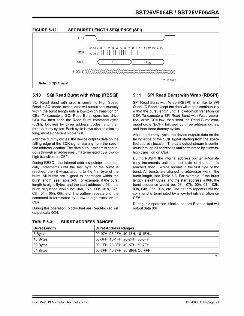
FIGURE 5-12: SET BURST LENGTH SEQUENCE (SPI)
5.10 SQI Read Burst with Wrap (RBSQI)SQI Read Burst with wrap is similar to High SpeedRead in SQI mode, except data will output continuouslywithin the burst length until a low-to-high transition onCE#. To execute a SQI Read Burst operation, driveCE# low then send the Read Burst command cycle(0CH), followed by three address cycles, and thenthree dummy cycles. Each cycle is two nibbles (clocks)long, most significant nibble first. After the dummy cycles, the device outputs data on thefalling edge of the SCK signal starting from the speci-fied address location. The data output stream is contin-uous through all addresses until terminated by a low-to-high transition on CE#. During RBSQI, the internal address pointer automati-cally increments until the last byte of the burst isreached, then it wraps around to the first byte of theburst. All bursts are aligned to addresses within theburst length, see Table 5-3. For example, if the burstlength is eight Bytes, and the start address is 06h, theburst sequence would be: 06h, 07h, 00h, 01h, 02h,03h, 04h, 05h, 06h, etc. The pattern repeats until thecommand is terminated by a low-to-high transition onCE#.During this operation, blocks that are Read-locked willoutput data 00H.
5.11 SPI Read Burst with Wrap (RBSPI)SPI Read Burst with Wrap (RBSPI) is similar to SPIQuad I/O Read except the data will output continuouslywithin the burst length until a low-to-high transition onCE#. To execute a SPI Read Burst with Wrap opera-tion, drive CE# low, then send the Read Burst com-mand cycle (ECH), followed by three address cycles,and then three dummy cycles. After the dummy cycle, the device outputs data on thefalling edge of the SCK signal starting from the speci-fied address location. The data output stream is contin-uous through all addresses until terminated by a low-to-high transition on CE#. During RBSPI, the internal address pointer automati-cally increments until the last byte of the burst isreached, then it wraps around to the first byte of theburst. All bursts are aligned to addresses within theburst length, see Table 5-3. For example, if the burstlength is eight Bytes, and the start address is 06h, theburst sequence would be: 06h, 07h, 00h, 01h, 02h,03h, 04h, 05h, 06h, etc. The pattern repeats until thecommand is terminated by a low-to-high transition onCE#.During this operation, blocks that are Read-locked willoutput data 00H.
CE#
SIO0
SCK0 1 2 3 4 5 6 7 8 12MODE 3
MODE 0
9 10 11
C0
25119 F51.0
SIO[3:1]
1513 14
DIN
Note: SIO[3:1] must
TABLE 5-3: BURST ADDRESS RANGESBurst Length Burst Address Ranges8 Bytes 00-07H, 08-0FH, 10-17H, 18-1FH...16 Bytes 00-0FH, 10-1FH, 20-2FH, 30-3FH...32 Bytes 00-1FH, 20-3FH, 40-5FH, 60-7FH...64 Bytes 00-3FH, 40-7FH, 80-BFH, C0-FFH
0
2015-2019 Microchip Technology Inc. DS20005119J-page 21
SST26VF064B / SST26VF064BA
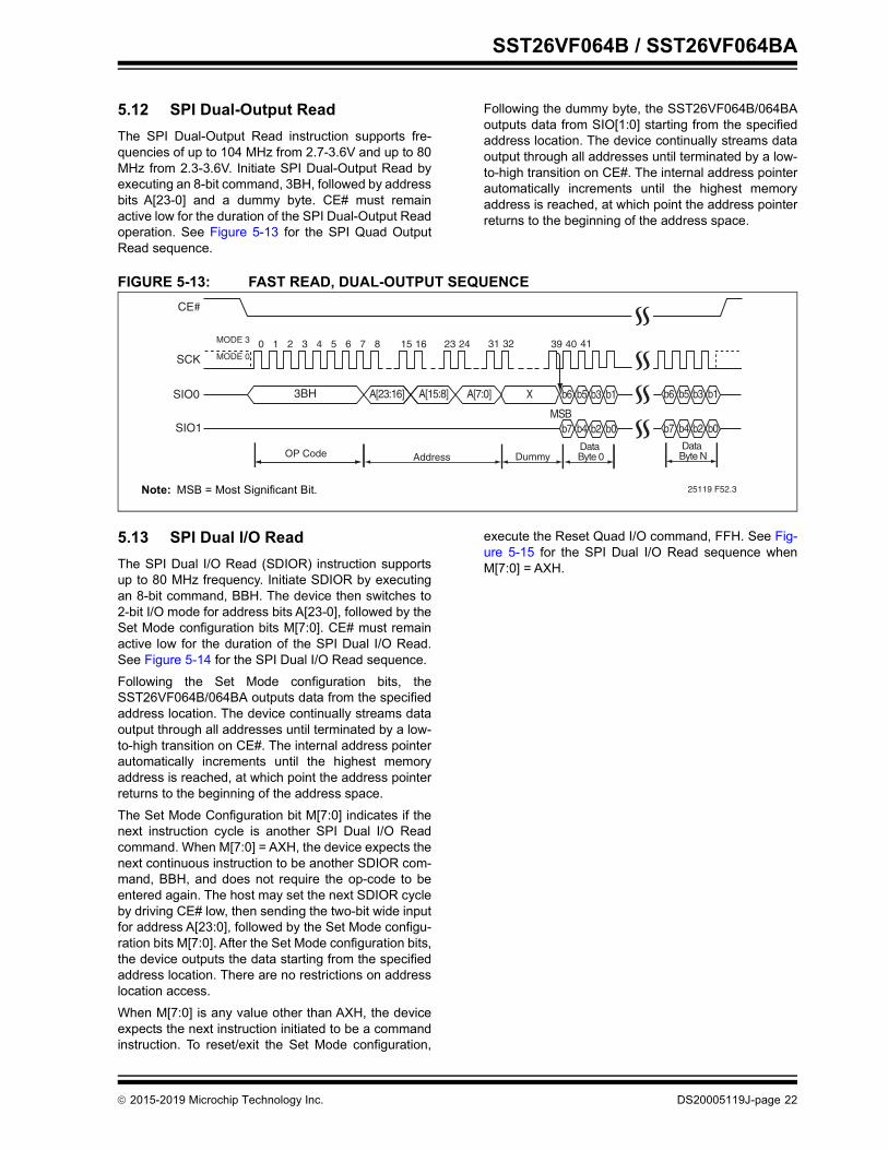
5.12 SPI Dual-Output ReadThe SPI Dual-Output Read instruction supports fre-quencies of up to 104 MHz from 2.7-3.6V and up to 80MHz from 2.3-3.6V. Initiate SPI Dual-Output Read byexecuting an 8-bit command, 3BH, followed by addressbits A[23-0] and a dummy byte. CE# must remainactive low for the duration of the SPI Dual-Output Readoperation. See Figure 5-13 for the SPI Quad OutputRead sequence.
Following the dummy byte, the SST26VF064B/064BAoutputs data from SIO[1:0] starting from the specifiedaddress location. The device continually streams dataoutput through all addresses until terminated by a low-to-high transition on CE#. The internal address pointerautomatically increments until the highest memoryaddress is reached, at which point the address pointerreturns to the beginning of the address space.
FIGURE 5-13: FAST READ, DUAL-OUTPUT SEQUENCE
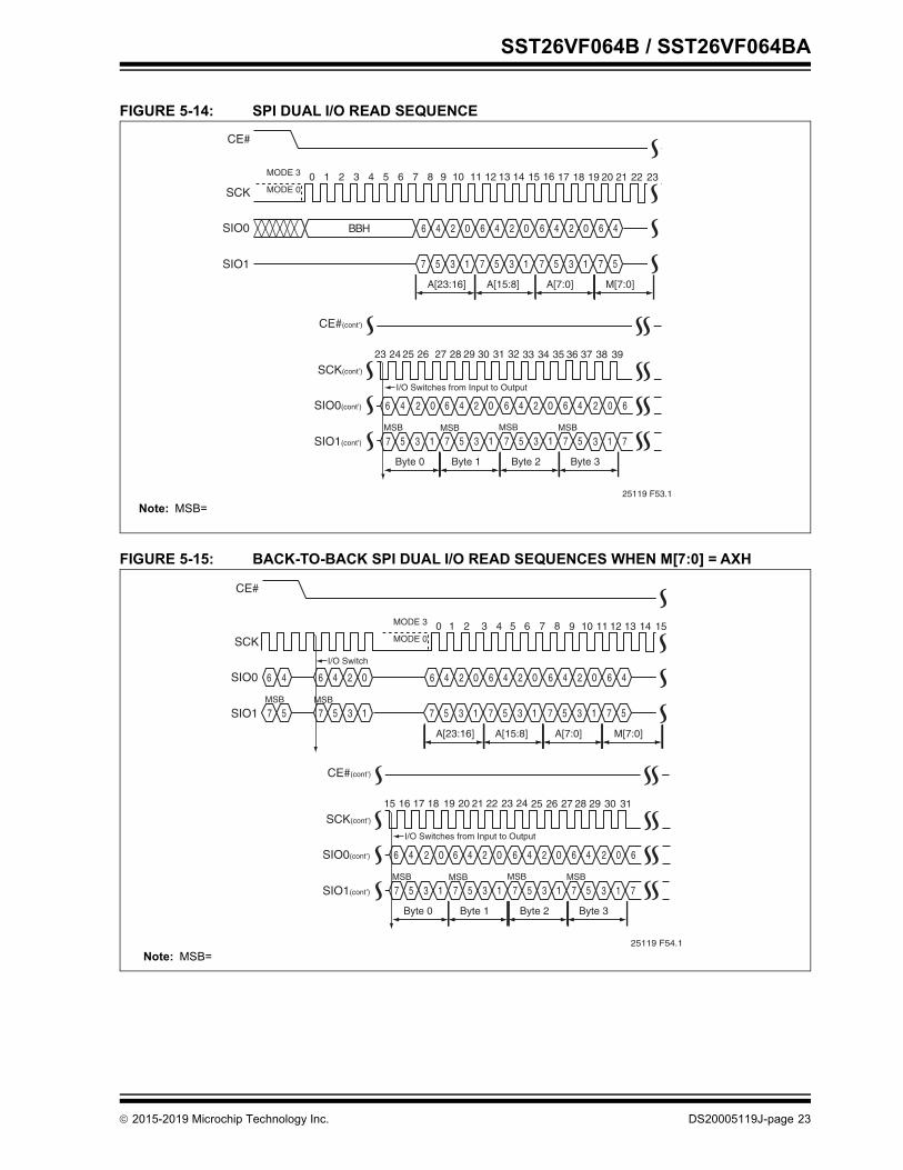
5.13 SPI Dual I/O ReadThe SPI Dual I/O Read (SDIOR) instruction supportsup to 80 MHz frequency. Initiate SDIOR by executingan 8-bit command, BBH. The device then switches to2-bit I/O mode for address bits A[23-0], followed by theSet Mode configuration bits M[7:0]. CE# must remainactive low for the duration of the SPI Dual I/O Read.See Figure 5-14 for the SPI Dual I/O Read sequence.Following the Set Mode configuration bits, theSST26VF064B/064BA outputs data from the specifiedaddress location. The device continually streams dataoutput through all addresses until terminated by a low-to-high transition on CE#. The internal address pointerautomatically increments until the highest memoryaddress is reached, at which point the address pointerreturns to the beginning of the address space. The Set Mode Configuration bit M[7:0] indicates if thenext instruction cycle is another SPI Dual I/O Readcommand. When M[7:0] = AXH, the device expects thenext continuous instruction to be another SDIOR com-mand, BBH, and does not require the op-code to beentered again. The host may set the next SDIOR cycleby driving CE# low, then sending the two-bit wide inputfor address A[23:0], followed by the Set Mode configu-ration bits M[7:0]. After the Set Mode configuration bits,the device outputs the data starting from the specifiedaddress location. There are no restrictions on addresslocation access. When M[7:0] is any value other than AXH, the deviceexpects the next instruction initiated to be a commandinstruction. To reset/exit the Set Mode configuration,
execute the Reset Quad I/O command, FFH. See Fig-ure 5-15 for the SPI Dual I/O Read sequence whenM[7:0] = AXH.
CE#
SIO0
SCK0 1 2 3 4 5 6 7 8 31 3224MODE 3
MODE 015 16 23
3BH
25119 F52.3
39 40 41
A[23:16] A[15:8] A[7:0] b6 b5 b6 b5
SIO1
AddressOP CodeData Byte 0Dummy
Data Byte N
b3 b1 b3 b1
b7 b4 b7 b4b2 b0 b2 b0MSB
X
Note: MSB = Most Significant Bit.
2015-2019 Microchip Technology Inc. DS20005119J-page 22
SST26VF064B / SST26VF064BA
FIGURE 5-14: SPI DUAL I/O READ SEQUENCE
FIGURE 5-15: BACK-TO-BACK SPI DUAL I/O READ SEQUENCES WHEN M[7:0] = AXH
7 5 3 1 7 5 3 1 7 5 3 1 7 5
6 4 2 0
CE#
SIO0
SCK0 1 2 3 4 5 6 7 8 16 1712MODE 3
MODE 09 10 11
25119 F53.1
SIO1
A[23:16]
1513 14 231918 2220 21
6 4 2 0 6 4 2 0 6 4
A[15:8] A[7:0] M[7:0]
7 5 3 1 7 5 3 1 7 5 3 1 7 5
4 2 0
CE#(cont’)
SIO0(cont’)
SCK(cont’)
23 24 32 332825 26 27
SIO1(cont’)
Byte 0
3129 30 393534 3836 37
6 4 2 0 6 4 2 0 6 4
Byte 1 Byte 2 Byte 3
2 0 6
3 1 7MSB MSB MSB
6
MSB
I/O Switches from Input to Output
BBH
Note: MSB=
7 5 3 1 7 5 3 1 7 5 3 1 7 5
MODE 3
MODE 0
6 4 2 0
CE#
SIO0
SCK0 8 941 2 3
25119 F54.1
SIO1
A[23:16]
75 6 151110 1412 13
6 4 2 0 6 4 2 0 6 4
A[15:8] A[7:0] M[7:0]
7 5 3 1 7 5 3 1 7 5 3 1 7 5
4 2 0
CE#(cont’)
SIO0(cont’)
SCK(cont’)
15 16 24 252017 18 19
SIO1(cont’)
Byte 0
2321 22 312726 3028 29
6 4 2 0 6 4 2 0 6 4
Byte 1 Byte 2 Byte 3
2 0 6
3 1 7MSB MSB MSB
6
MSB
7 5 7 5 3 1
4 6 4 2 0
MSB
6
MSB
I/O Switches from Input to Output
I/O Switch
Note: MSB=
2015-2019 Microchip Technology Inc. DS20005119J-page 23
SST26VF064B / SST26VF064BA
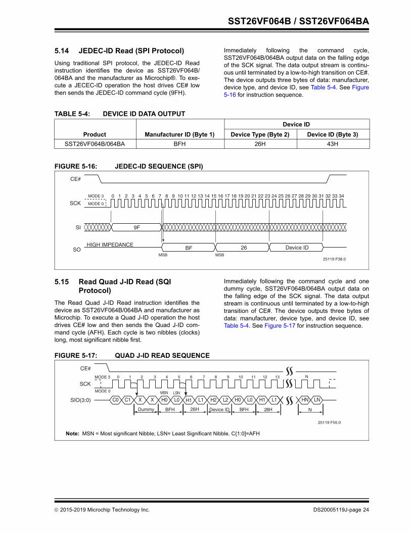
5.14 JEDEC-ID Read (SPI Protocol)Using traditional SPI protocol, the JEDEC-ID Readinstruction identifies the device as SST26VF064B/064BA and the manufacturer as Microchip®. To exe-cute a JECEC-ID operation the host drives CE# lowthen sends the JEDEC-ID command cycle (9FH).
Immediately following the command cycle,SST26VF064B/064BA output data on the falling edgeof the SCK signal. The data output stream is continu-ous until terminated by a low-to-high transition on CE#.The device outputs three bytes of data: manufacturer,device type, and device ID, see Table 5-4. See Figure5-16 for instruction sequence.
FIGURE 5-16: JEDEC-ID SEQUENCE (SPI)
5.15 Read Quad J-ID Read (SQI Protocol)
The Read Quad J-ID Read instruction identifies thedevice as SST26VF064B/064BA and manufacturer asMicrochip. To execute a Quad J-ID operation the hostdrives CE# low and then sends the Quad J-ID com-mand cycle (AFH). Each cycle is two nibbles (clocks)long, most significant nibble first.
Immediately following the command cycle and onedummy cycle, SST26VF064B/064BA output data onthe falling edge of the SCK signal. The data outputstream is continuous until terminated by a low-to-hightransition of CE#. The device outputs three bytes ofdata: manufacturer, device type, and device ID, seeTable 5-4. See Figure 5-17 for instruction sequence.
FIGURE 5-17: QUAD J-ID READ SEQUENCE
TABLE 5-4: DEVICE ID DATA OUTPUT
Product Manufacturer ID (Byte 1)Device ID
Device Type (Byte 2) Device ID (Byte 3)SST26VF064B/064BA BFH 26H 43H
26 Device ID
25119 F38.0
CE#
SO
SI
SCK0 1 2 3 4 5 6 7 8
HIGH IMPEDANCE
15 1614 28 29 30 31
BF
MODE 3
MODE 0
MSBMSB
9 10 11 12 13 17 18 32 34
9F
19 20 21 22 23 3324 25 26 27
BFH Device IDDummy BFH
MSN LSN
26H26H N
25119 F55.0
0 1 2
SCK
SIO(3:0)
CE#
C1C0 X X H0 L0 H1 L1 H0 L1H1L0 HN LN
7 8 11109 1312 NMODE 3
MODE 0
3 4 5 6
H2 L2
Note: MSN = Most significant Nibble; LSN= Least Significant Nibble. C{1:0]=AFH
2015-2019 Microchip Technology Inc. DS20005119J-page 24
SST26VF064B / SST26VF064BA
5.16 Serial Flash Discoverable Parameters (SFDP)
The Serial Flash Discoverable Parameters (SFDP)contain information describing the characteristics of thedevice. This allows device-independent, JEDEC ID-independent, and forward/backward compatible soft-
ware support for all future Serial Flash device families.See Table 11-1 on page 65 for address and data val-ues.Initiate SFDP by executing an 8-bit command, 5AH, fol-lowed by address bits A[23-0] and a dummy byte. CE#must remain active low for the duration of the SFDPcycle. For the SFDP sequence, see Figure 5-18.
FIGURE 5-18: SERIAL FLASH DISCOVERABLE PARAMETERS SEQUENCE
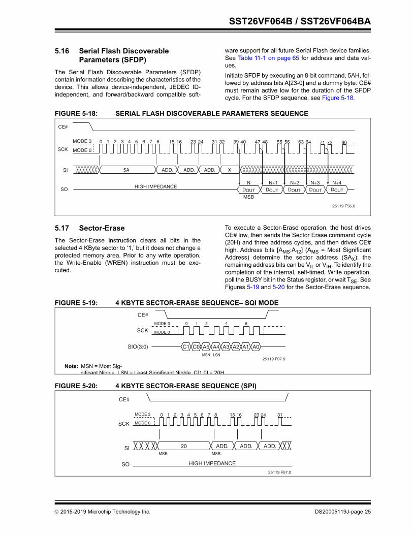
5.17 Sector-EraseThe Sector-Erase instruction clears all bits in theselected 4 KByte sector to ‘1,’ but it does not change aprotected memory area. Prior to any write operation,the Write-Enable (WREN) instruction must be exe-cuted.
To execute a Sector-Erase operation, the host drivesCE# low, then sends the Sector Erase command cycle(20H) and three address cycles, and then drives CE#high. Address bits [AMS:A12] (AMS = Most SignificantAddress) determine the sector address (SAX); theremaining address bits can be VIL or VIH. To identify thecompletion of the internal, self-timed, Write operation,poll the BUSY bit in the Status register, or wait TSE. SeeFigures 5-19 and 5-20 for the Sector-Erase sequence.
FIGURE 5-19: 4 KBYTE SECTOR-ERASE SEQUENCE– SQI MODE
FIGURE 5-20: 4 KBYTE SECTOR-ERASE SEQUENCE (SPI)
25119 F56.0
CE#
SO
SI
SCK
ADD.
0 1 2 3 4 5 6 7 8
ADD. ADD.5A
HIGH IMPEDANCE
15 16 23 24 31 32 39 40 47 48 55 56 63 64
N+2 N+3 N+4N N+1
X
MSB
MODE 0
MODE 3
DOUT DOUT DOUT DOUT
8071 72
DOUT
25119 F07.0
MODE 3 0 1
SCK
SIO(3:0)
CE#
C1 C0
MODE 0
2
A5 A4MSN LSN
4
A3 A2
6
A1 A0
Note: MSN = Most Sig-nificant Nibble, LSN = Least Significant Nibble, C[1:0] = 20H
CE#
SO
SI
SCK
ADD.
0 1 2 3 4 5 6 7 8
ADD. ADD.20
HIGH IMPEDANCE
15 16 23 24 31
MODE 0
MODE 3
25119 F57.0
MSBMSB
2015-2019 Microchip Technology Inc. DS20005119J-page 25
SST26VF064B / SST26VF064BA
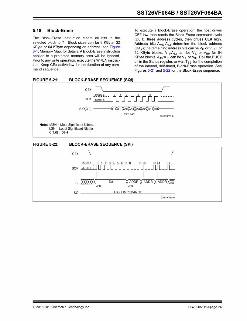
5.18 Block-EraseThe Block-Erase instruction clears all bits in theselected block to ‘1’. Block sizes can be 8 KByte, 32KByte or 64 KByte depending on address, see Figure3-1, Memory Map, for details. A Block-Erase instructionapplied to a protected memory area will be ignored.Prior to any write operation, execute the WREN instruc-tion. Keep CE# active low for the duration of any com-mand sequence.
To execute a Block-Erase operation, the host drivesCE# low then sends the Block-Erase command cycle(D8H), three address cycles, then drives CE# high.Address bits AMS-A13 determine the block address(BAX); the remaining address bits can be VIL or VIH. For32 KByte blocks, A14:A13 can be VIL or VIH; for 64KByte blocks, A15:A13 can be VIL or VIH. Poll the BUSYbit in the Status register, or wait TBE, for the completionof the internal, self-timed, Block-Erase operation. SeeFigures 5-21 and 5-22 for the Block-Erase sequence.
FIGURE 5-21: BLOCK-ERASE SEQUENCE (SQI)
FIGURE 5-22: BLOCK-ERASE SEQUENCE (SPI)
25119 F08.0
MODE 3 0 1
SCK
SIO(3:0)
CE#
C1 C0
MODE 0
2
A5 A4MSN LSN
4
A3 A2
6
A1 A0
Note: MSN = Most Significant Nibble, LSN = Least Significant NibbleC[1:0] = D8H
CE#
SO
SI
SCK
ADDR
0 1 2 3 4 5 6 7 8
ADDR ADDRD8
HIGH IMPEDANCE
15 16 23 24 31
MODE 0
MODE 3
25119 F58.0
MSB MSB
2015-2019 Microchip Technology Inc. DS20005119J-page 26
SST26VF064B / SST26VF064BA
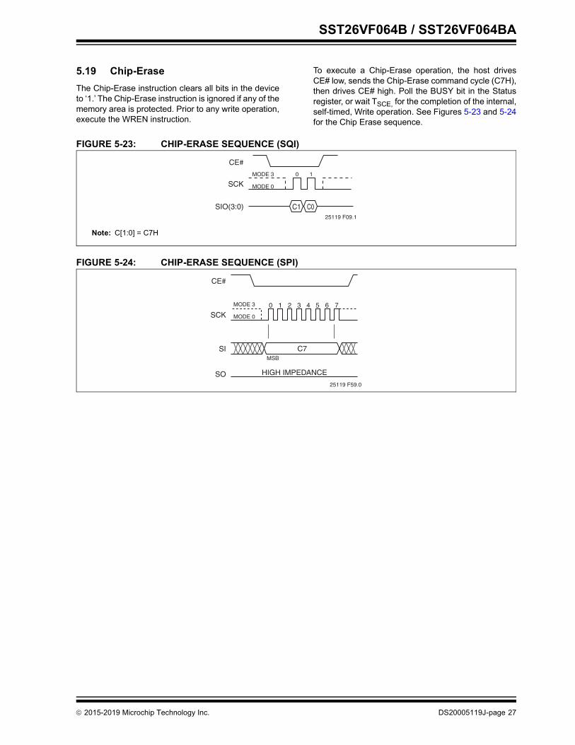
5.19 Chip-EraseThe Chip-Erase instruction clears all bits in the deviceto ‘1.’ The Chip-Erase instruction is ignored if any of thememory area is protected. Prior to any write operation,execute the WREN instruction.
To execute a Chip-Erase operation, the host drivesCE# low, sends the Chip-Erase command cycle (C7H),then drives CE# high. Poll the BUSY bit in the Statusregister, or wait TSCE, for the completion of the internal,self-timed, Write operation. See Figures 5-23 and 5-24for the Chip Erase sequence.
FIGURE 5-23: CHIP-ERASE SEQUENCE (SQI)
FIGURE 5-24: CHIP-ERASE SEQUENCE (SPI)
25119 F09.1
MODE 3 0 1
SCK
SIO(3:0)
CE#
C1 C0
MODE 0
Note: C[1:0] = C7H
CE#
SO
SI
SCK0 1 2 3 4 5 6 7
C7
HIGH IMPEDANCE
MODE 0
MODE 3
25119 F59.0
MSB
2015-2019 Microchip Technology Inc. DS20005119J-page 27
SST26VF064B / SST26VF064BA
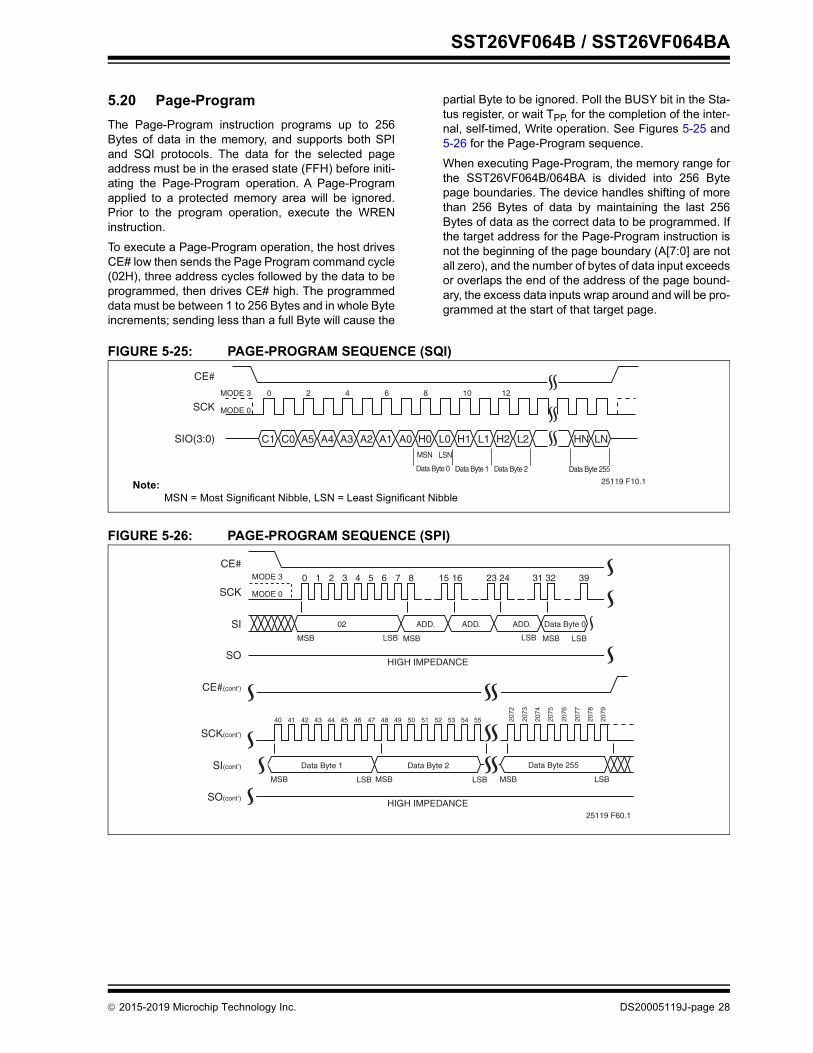
5.20 Page-ProgramThe Page-Program instruction programs up to 256Bytes of data in the memory, and supports both SPIand SQI protocols. The data for the selected pageaddress must be in the erased state (FFH) before initi-ating the Page-Program operation. A Page-Programapplied to a protected memory area will be ignored.Prior to the program operation, execute the WRENinstruction. To execute a Page-Program operation, the host drivesCE# low then sends the Page Program command cycle(02H), three address cycles followed by the data to beprogrammed, then drives CE# high. The programmeddata must be between 1 to 256 Bytes and in whole Byteincrements; sending less than a full Byte will cause the
partial Byte to be ignored. Poll the BUSY bit in the Sta-tus register, or wait TPP, for the completion of the inter-nal, self-timed, Write operation. See Figures 5-25 and5-26 for the Page-Program sequence.When executing Page-Program, the memory range forthe SST26VF064B/064BA is divided into 256 Bytepage boundaries. The device handles shifting of morethan 256 Bytes of data by maintaining the last 256Bytes of data as the correct data to be programmed. Ifthe target address for the Page-Program instruction isnot the beginning of the page boundary (A[7:0] are notall zero), and the number of bytes of data input exceedsor overlaps the end of the address of the page bound-ary, the excess data inputs wrap around and will be pro-grammed at the start of that target page.
FIGURE 5-25: PAGE-PROGRAM SEQUENCE (SQI)
FIGURE 5-26: PAGE-PROGRAM SEQUENCE (SPI)
25119 F10.1
MODE 3 0
SCK
SIO(3:0)
CE#
C1 C0
MODE 0
2
A5 A4MSN LSN
4
A3 A2
6
A1 A0
8
H0 L0
10
H1 L1
12
H2 L2 HN LN
Data Byte 0 Data Byte 1 Data Byte 2 Data Byte 255
Note:MSN = Most Significant Nibble, LSN = Least Significant Nibble
25119 F60.1
CE#
SO
SI
SCK
ADD.
0 1 2 3 4 5 6 7 8
ADD. ADD. Data Byte 002
HIGH IMPEDANCE
15 16 23 24 31 32 39
MODE 0
MODE 3
MSBMSBMSB LSB
CE#(cont’)
SO(cont’)
SI(cont’)
SCK(cont’)
40 41 42 43 44 45 46 47 48
Data Byte 1
HIGH IMPEDANCE
MSBMSBMSB LSB
50 51 52 53 54 55 2072
49
Data Byte 2
2073
2074
2075
2076
2077
2078
2079
Data Byte 255
LSBLSB
LSB LSB
2015-2019 Microchip Technology Inc. DS20005119J-page 28
SST26VF064B / SST26VF064BA
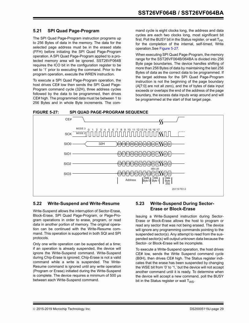
5.21 SPI Quad Page-ProgramThe SPI Quad Page-Program instruction programs upto 256 Bytes of data in the memory. The data for theselected page address must be in the erased state(FFH) before initiating the SPI Quad Page-Programoperation. A SPI Quad Page-Program applied to a pro-tected memory area will be ignored. SST26VF064Brequires the ICO bit in the configuration register to beset to ‘1’ prior to executing the command. Prior to theprogram operation, execute the WREN instruction. To execute a SPI Quad Page-Program operation, thehost drives CE# low then sends the SPI Quad Page-Program command cycle (32H), three address cyclesfollowed by the data to be programmed, then drivesCE# high. The programmed data must be between 1 to256 Bytes and in whole Byte increments. The com-
mand cycle is eight clocks long, the address and datacycles are each two clocks long, most significant bitfirst. Poll the BUSY bit in the Status register, or wait TPP,for the completion of the internal, self-timed, Writeoperation.See Figure 5-27.When executing SPI Quad Page-Program, the memoryrange for the SST26VF064B/064BA is divided into 256Byte page boundaries. The device handles shifting ofmore than 256 Bytes of data by maintaining the last 256Bytes of data as the correct data to be programmed. Ifthe target address for the SPI Quad Page-Programinstruction is not the beginning of the page boundary(A[7:0] are not all zero), and the of bytes of data inputexceeds or overlaps the end of the address of the pageboundary, the excess data inputs wrap around and willbe programmed at the start of that target page.
FIGURE 5-27: SPI QUAD PAGE-PROGRAM SEQUENCE
5.22 Write-Suspend and Write-ResumeWrite-Suspend allows the interruption of Sector-Erase,Block-Erase, SPI Quad Page-Program, or Page-Pro-gram operations in order to erase, program, or readdata in another portion of memory. The original opera-tion can be continued with the Write-Resume com-mand. This operation is supported in both SQI and SPIprotocols. Only one write operation can be suspended at a time;if an operation is already suspended, the device willignore the Write-Suspend command. Write-Suspendduring Chip-Erase is ignored; Chip-Erase is not a validcommand while a write is suspended. The Write-Resume command is ignored until any write operation(Program or Erase) initiated during the Write-Suspendis complete. The device requires a minimum of 500 µsbetween each Write-Suspend command.
5.23 Write-Suspend During Sector-Erase or Block-Erase
Issuing a Write-Suspend instruction during Sector-Erase or Block-Erase allows the host to program orread any sector that was not being erased. The devicewill ignore any programming commands pointing to thesuspended sector(s). Any attempt to read from the sus-pended sector(s) will output unknown data because theSector- or Block-Erase will be incomplete. To execute a Write-Suspend operation, the host drivesCE# low, sends the Write Suspend command cycle(B0H), then drives CE# high. The Status register indi-cates that the erase has been suspended by changingthe WSE bit from ‘0’ to ‘1,’ but the device will not acceptanother command until it is ready. To determine whenthe device will accept a new command, poll the BUSYbit in the Status register or wait TWS.
A20A16A12 A8 A4 A0 b4 b0
CE#
SIO0
SCK0 1 2 3 4 5 6 7 8 16 1712MODE 3
MODE 09 10 11
32H
25119 F61.0
SIO1
SIO2
SIO3
AddressData Byte 1
1513 14
A21 A17A13 A9 A5 A1 b5 b1 b5 b1 b5 b1
A22 A18A14A10 A6 A2 b6 b2 b6 b2 b6 b2
A23 A19 A15 A11 A7 A3 b7 b3 b7 b3 b7 b3Data
Byte 0Data Byte 255
MSN LSN
b4 b0 b4 b0
2015-2019 Microchip Technology Inc. DS20005119J-page 29
SST26VF064B / SST26VF064BA
5.24 Write Suspend During Page Programming or SPI Quad Page Programming
Issuing a Write-Suspend instruction during Page Pro-gramming allows the host to erase or read any sectorthat is not being programmed. Erase commands point-ing to the suspended sector(s) will be ignored. Anyattempt to read from the suspended page will outputunknown data because the program will be incomplete. To execute a Write Suspend operation, the host drivesCE# low, sends the Write Suspend command cycle(B0H), then drives CE# high. The Status register indi-cates that the programming has been suspended bychanging the WSP bit from ‘0’ to ‘1,’ but the device willnot accept another command until it is ready. To deter-mine when the device will accept a new command, pollthe BUSY bit in the Status register or wait TWS.
5.25 Write-ResumeWrite-Resume restarts a Write command that was sus-pended, and changes the suspend status bit in the Sta-tus register (WSE or WSP) back to ‘0’. To execute a Write-Resume operation, the host drivesCE# low, sends the Write Resume command cycle(30H), then drives CE# high. To determine if the inter-nal, self-timed Write operation completed, poll theBUSY bit in the Status register, or wait the specifiedtime TSE, TBE or TPP for Sector-Erase, Block-Erase, orPage-Programming, respectively. The total write timebefore suspend and after resume will not exceed theuninterrupted write times TSE, TBE or TPP.
5.26 Read Security IDThe Read Security ID operation is supported in bothSPI and SQI modes. To execute a Read Security ID(SID) operation in SPI mode, the host drives CE# low,sends the Read Security ID command cycle (88H), twoaddress cycles, and then one dummy cycle. To execute
a Read Security ID operation in SQI mode, the hostdrives CE# low and then sends the Read Security IDcommand, two address cycles, and three dummycycles.After the dummy cycles, the device outputs data on thefalling edge of the SCK signal, starting from the speci-fied address location. The data output stream is contin-uous through all SID addresses until terminated by alow-to-high transition on CE#. See Table 5-5 for theSecurity ID address range.
5.27 Program Security IDThe Program Security ID instruction programs one to2040 Bytes of data in the user-programmable, SecurityID space. This Security ID space is one-time program-mable (OTP). The device ignores a Program SecurityID instruction pointing to an invalid or protectedaddress, see Table 5-5. Prior to the program operation,execute WREN. To execute a Program SID operation, the host drivesCE# low, sends the Program Security ID commandcycle (A5H), two address cycles, the data to be pro-grammed, then drives CE# high. The programmed datamust be between 1 to 256 Bytes and in whole Byteincrements. The device handles shifting of more than 256 Bytes ofdata by maintaining the last 256 Bytes of data as thecorrect data to be programmed. If the target address forthe Program Security ID instruction is not the beginningof the page boundary, and the number of data inputexceeds or overlaps the end of the address of the pageboundary, the excess data inputs wrap around and willbe programmed at the start of that target page.The Program Security ID operation is supported in bothSPI and SQI mode. To determine the completion of theinternal, self-timed Program SID operation, poll theBUSY bit in the software status register, or wait TPSIDfor the completion of the internal self-timed ProgramSecurity ID operation.
TABLE 5-5: PROGRAM SECURITY IDProgram Security ID Address RangeUnique ID Pre-Programmed at factory 0000 – 0007HUser Programmable 0008H – 07FFH
2015-2019 Microchip Technology Inc. DS20005119J-page 30
SST26VF064B / SST26VF064BA
5.28 Lockout Security IDThe Lockout Security ID instruction prevents any futurechanges to the Security ID, and is supported in bothSPI and SQI modes. Prior to the operation, executeWREN.To execute a Lockout SID, the host drives CE# low,sends the Lockout Security ID command cycle (85H),then drives CE# high. Poll the BUSY bit in the softwarestatus register, or wait TPSID, for the completion of theLockout Security ID operation.
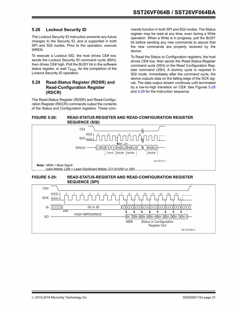
5.29 Read-Status Register (RDSR) and Read-Configuration Register (RDCR)
The Read-Status Register (RDSR) and Read-Configu-ration Register (RDCR) commands output the contentsof the Status and Configuration registers. These com-
mands function in both SPI and SQI modes. The Statusregister may be read at any time, even during a Writeoperation. When a Write is in progress, poll the BUSYbit before sending any new commands to assure thatthe new commands are properly received by thedevice. To Read the Status or Configuration registers, the hostdrives CE# low, then sends the Read-Status-Registercommand cycle (05H) or the Read Configuration Reg-ister command (35H). A dummy cycle is required inSQI mode. Immediately after the command cycle, thedevice outputs data on the falling edge of the SCK sig-nal. The data output stream continues until terminatedby a low-to-high transition on CE#. See Figures 5-28and 5-29 for the instruction sequence.
FIGURE 5-28: READ-STATUS-REGISTER AND READ-CONFIGURATION REGISTER SEQUENCE (SQI)
FIGURE 5-29: READ-STATUS-REGISTER AND READ-CONFIGURATION REGISTER SEQUENCE (SPI)
25119 F11.1
MODE 3 0
SCK
SIO(3:0)
CE#
C1 C0
MODE 0
2
X XMSN LSN
4
H0 L0
6
H0 L0
8
H0 L0
Dummy Data Byte Data Byte Data Byte
Note: MSN = Most Signif-icant Nibble; LSN = Least Significant Nibble, C[1:0]=05H or 35H
0 1 2 3 4 5 6 7 8 9 10 11 12 13 14
25119 F62.0
MODE 3
SCK
SI
SO
CE#
Bit 7 Bit 6 Bit 5 Bit 4 Bit 3 Bit 2 Bit 1 Bit 0
05 or 35
MODE 0
HIGH IMPEDANCE
Status or ConfigurationRegister Out
MSB
MSB
2015-2019 Microchip Technology Inc. DS20005119J-page 31
SST26VF064B / SST26VF064BA
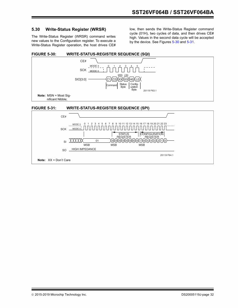
5.30 Write-Status Register (WRSR)The Write-Status Register (WRSR) command writesnew values to the Configuration register. To execute aWrite-Status Register operation, the host drives CE#
low, then sends the Write-Status Register commandcycle (01H), two cycles of data, and then drives CE#high. Values in the second data cycle will be acceptedby the device. See Figures 5-30 and 5-31.
FIGURE 5-30: WRITE-STATUS-REGISTER SEQUENCE (SQI)
FIGURE 5-31: WRITE-STATUS-REGISTER SEQUENCE (SPI)
25119 F63.1
MODE 3 0 1
SCK
SIO[3:0]
CE#
C1 C0
MODE 0
2
XX XX
MSN LSN
4
H0 L0
53
StatusByte
Command Config-uration Byte
Note: MSN = Most Sig-nificant Nibble;
25119 F64.1
MODE 3
HIGH IMPEDANCE
MODE 0
STATUSREGISTER
XX
MSBMSB
01
SCK
SI
SO
CE#
0 1 2 3 4 5 6 7 8 9 10 11 12 13 14 15
CONFIGURATIONREGISTER
7 6 5 4 3 2 1 0
MSB
16 17 18 19 20 21 22 23
XX XX XX XX XX XX XX
Note: XX = Don’t Care
2015-2019 Microchip Technology Inc. DS20005119J-page 32
SST26VF064B / SST26VF064BA
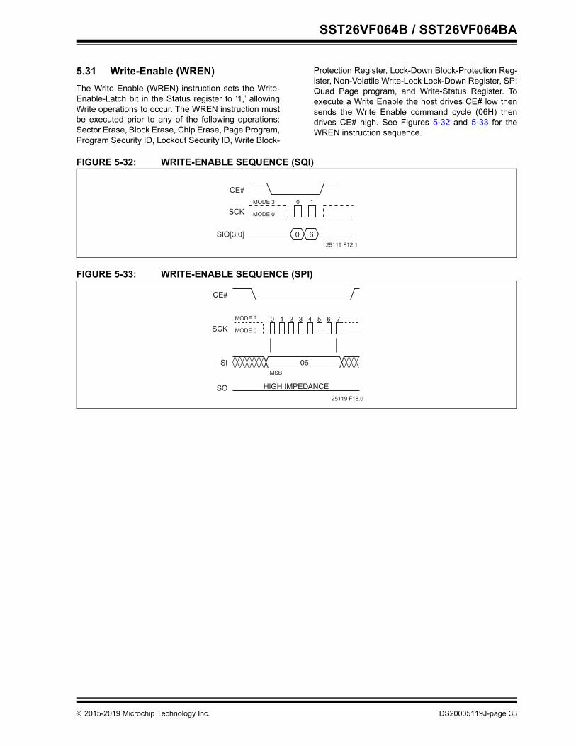
5.31 Write-Enable (WREN)The Write Enable (WREN) instruction sets the Write-Enable-Latch bit in the Status register to ‘1,’ allowingWrite operations to occur. The WREN instruction mustbe executed prior to any of the following operations:Sector Erase, Block Erase, Chip Erase, Page Program,Program Security ID, Lockout Security ID, Write Block-
Protection Register, Lock-Down Block-Protection Reg-ister, Non-Volatile Write-Lock Lock-Down Register, SPIQuad Page program, and Write-Status Register. Toexecute a Write Enable the host drives CE# low thensends the Write Enable command cycle (06H) thendrives CE# high. See Figures 5-32 and 5-33 for theWREN instruction sequence.
FIGURE 5-32: WRITE-ENABLE SEQUENCE (SQI)
FIGURE 5-33: WRITE-ENABLE SEQUENCE (SPI)
25119 F12.1
MODE 3 0 1
SCK
SIO[3:0]
CE#
0 6
MODE 0
CE#
SO
SI
SCK0 1 2 3 4 5 6 7
06
HIGH IMPEDANCE
MODE 0
MODE 3
25119 F18.0
MSB
2015-2019 Microchip Technology Inc. DS20005119J-page 33
SST26VF064B / SST26VF064BA
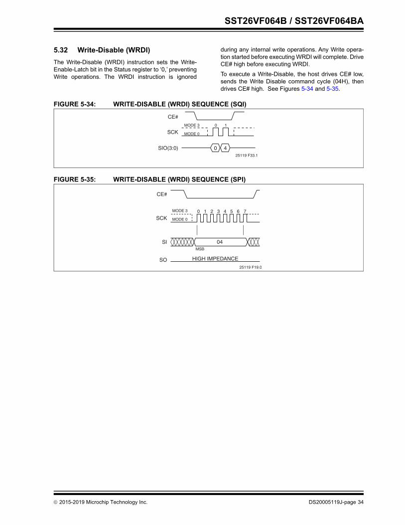
5.32 Write-Disable (WRDI)The Write-Disable (WRDI) instruction sets the Write-Enable-Latch bit in the Status register to ‘0,’ preventingWrite operations. The WRDI instruction is ignored
during any internal write operations. Any Write opera-tion started before executing WRDI will complete. DriveCE# high before executing WRDI. To execute a Write-Disable, the host drives CE# low,sends the Write Disable command cycle (04H), thendrives CE# high. See Figures 5-34 and 5-35.
FIGURE 5-34: WRITE-DISABLE (WRDI) SEQUENCE (SQI)
FIGURE 5-35: WRITE-DISABLE (WRDI) SEQUENCE (SPI)
25119 F33.1
MODE 3 0 1
SCK
SIO(3:0)
CE#
0 4
MODE 0
CE#
SO
SI
SCK0 1 2 3 4 5 6 7
04
HIGH IMPEDANCE
MODE 0
MODE 3
25119 F19.0
MSB
2015-2019 Microchip Technology Inc. DS20005119J-page 34
SST26VF064B / SST26VF064BA
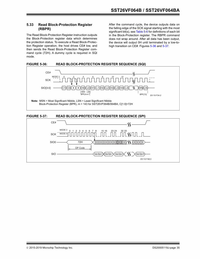
5.33 Read Block-Protection Register (RBPR)
The Read Block-Protection Register instruction outputsthe Block-Protection register data which determinesthe protection status. To execute a Read Block-Protec-tion Register operation, the host drives CE# low, andthen sends the Read Block-Protection Register com-mand cycle (72H). A dummy cycle is required in SQImode.
After the command cycle, the device outputs data onthe falling edge of the SCK signal starting with the mostsignificant bit(s), see Table 5-6 for definitions of each bitin the Block-Protection register. The RBPR commanddoes not wrap around. After all data has been output,the device will output 0H until terminated by a low-to-high transition on CE#. Figures 5-36 and 5-37.
FIGURE 5-36: READ BLOCK-PROTECTION REGISTER SEQUENCE (SQI)
FIGURE 5-37: READ BLOCK-PROTECTION REGISTER SEQUENCE (SPI)
25119 F34.2
MODE 3 0
SCK
SIO[3:0]
CE#
C1 C0
2
H0 L0MSN LSN
4
H1 L1
6
H2 L2
8
H3 L3
10
H4 L4
12
HN LN
BPR [m:m-7] BPR [7:0]
X X
Note: MSN = Most Significant Nibble, LSN = Least Significant NibbleBlock-Protection Register (BPR), m = 143 for SST26VF064B/064BA, C[1:0]=72H
CE#
SIO0
SCK0 1 2 3 4 5 6 7 8 32 3324MODE 3
MODE 015 16 23
72H
25119 F48.0
SIO
OP Code
Data Byte 0 Data Byte 1 Data Byte 2 Data Byte N
2015-2019 Microchip Technology Inc. DS20005119J-page 35
SST26VF064B / SST26VF064BA
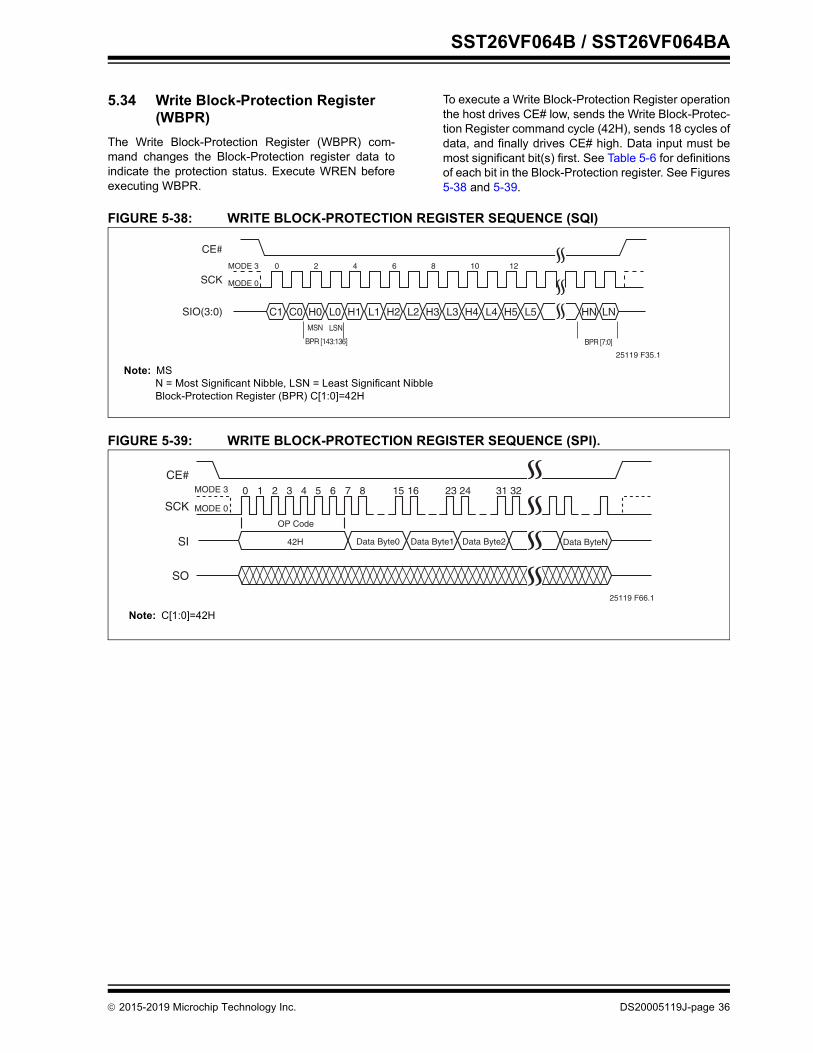
5.34 Write Block-Protection Register (WBPR)
The Write Block-Protection Register (WBPR) com-mand changes the Block-Protection register data toindicate the protection status. Execute WREN beforeexecuting WBPR.
To execute a Write Block-Protection Register operationthe host drives CE# low, sends the Write Block-Protec-tion Register command cycle (42H), sends 18 cycles ofdata, and finally drives CE# high. Data input must bemost significant bit(s) first. See Table 5-6 for definitionsof each bit in the Block-Protection register. See Figures5-38 and 5-39.
FIGURE 5-38: WRITE BLOCK-PROTECTION REGISTER SEQUENCE (SQI)
FIGURE 5-39: WRITE BLOCK-PROTECTION REGISTER SEQUENCE (SPI).
25119 F35.1
MODE 3 0
SCK
SIO(3:0)
CE#
C1 C0
MODE 0
2
H0 L0MSN LSN
4
H1 L1
6
H2 L2
8
H3 L3
10
H4 L4
12
H5 L5 HN LN
BPR [143:136] BPR [7:0]
Note: MSN = Most Significant Nibble, LSN = Least Significant NibbleBlock-Protection Register (BPR) C[1:0]=42H
CE#
SO
SI
SCK
Data Byte0
0 1 2 3 4 5 6 7 8
Data Byte1 Data Byte2 Data ByteN42H
15 16 23 24 31 32
MODE 0
MODE 3
OP Code
25119 F66.1
Note: C[1:0]=42H
2015-2019 Microchip Technology Inc. DS20005119J-page 36
SST26VF064B / SST26VF064BA
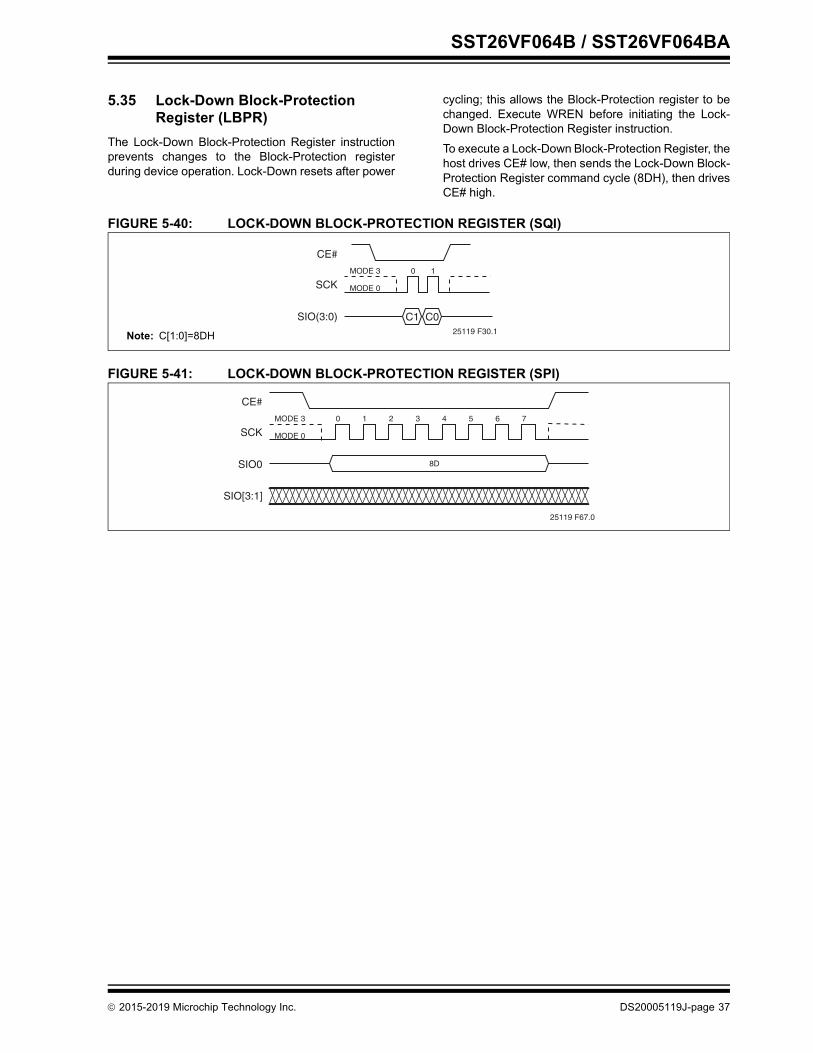
5.35 Lock-Down Block-Protection Register (LBPR)
The Lock-Down Block-Protection Register instructionprevents changes to the Block-Protection registerduring device operation. Lock-Down resets after power
cycling; this allows the Block-Protection register to bechanged. Execute WREN before initiating the Lock-Down Block-Protection Register instruction.To execute a Lock-Down Block-Protection Register, thehost drives CE# low, then sends the Lock-Down Block-Protection Register command cycle (8DH), then drivesCE# high.
FIGURE 5-40: LOCK-DOWN BLOCK-PROTECTION REGISTER (SQI)
FIGURE 5-41: LOCK-DOWN BLOCK-PROTECTION REGISTER (SPI)
25119 F30.1
MODE 3 0 1
SCK
SIO(3:0)
CE#
C1 C0
MODE 0
Note: C[1:0]=8DH
25119 F67.0
MODE 3 0 1
SCK
SIO0
CE#
MODE 0
2 3 4 5 6 7
8D
SIO[3:1]
2015-2019 Microchip Technology Inc. DS20005119J-page 37
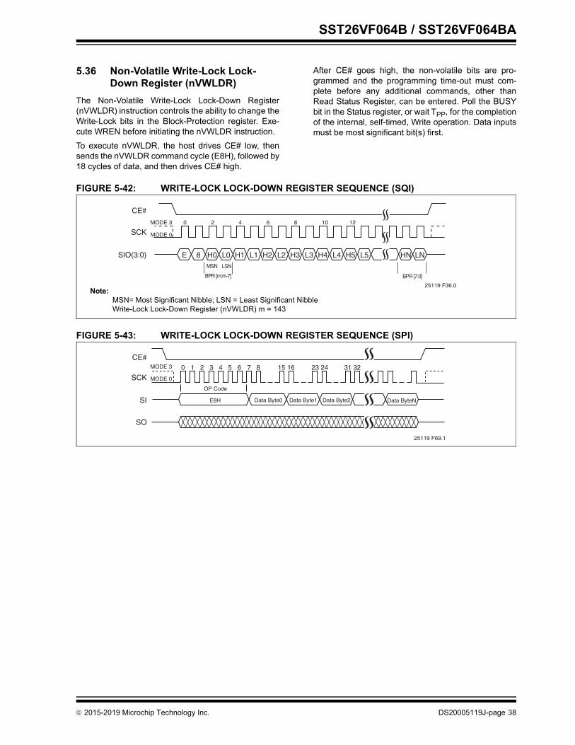
SST26VF064B / SST26VF064BA
5.36 Non-Volatile Write-Lock Lock-Down Register (nVWLDR)
The Non-Volatile Write-Lock Lock-Down Register(nVWLDR) instruction controls the ability to change theWrite-Lock bits in the Block-Protection register. Exe-cute WREN before initiating the nVWLDR instruction.To execute nVWLDR, the host drives CE# low, thensends the nVWLDR command cycle (E8H), followed by18 cycles of data, and then drives CE# high.
After CE# goes high, the non-volatile bits are pro-grammed and the programming time-out must com-plete before any additional commands, other thanRead Status Register, can be entered. Poll the BUSYbit in the Status register, or wait TPP, for the completionof the internal, self-timed, Write operation. Data inputsmust be most significant bit(s) first.
FIGURE 5-42: WRITE-LOCK LOCK-DOWN REGISTER SEQUENCE (SQI)
FIGURE 5-43: WRITE-LOCK LOCK-DOWN REGISTER SEQUENCE (SPI)
25119 F36.0
MODE 3 0
SCK
SIO(3:0)
CE#
E 8
MODE 0
2
H0 L0MSN LSN
4
H1 L1
6
H2 L2
8
H3 L3
10
H4 L4
12
H5 L5 HN LN
BPR [m:m-7] BPR [7:0]
Note:MSN= Most Significant Nibble; LSN = Least Significant NibbleWrite-Lock Lock-Down Register (nVWLDR) m = 143
CE#
SO
SI
SCK
Data Byte0
0 1 2 3 4 5 6 7 8
Data Byte1 Data Byte2 Data ByteNE8H
15 16 23 24 31 32
MODE 0
MODE 3
OP Code
25119 F69.1
2015-2019 Microchip Technology Inc. DS20005119J-page 38
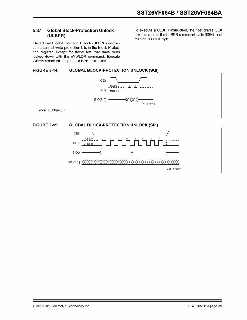
SST26VF064B / SST26VF064BA
5.37 Global Block-Protection Unlock (ULBPR)
The Global Block-Protection Unlock (ULBPR) instruc-tion clears all write-protection bits in the Block-Protec-tion register, except for those bits that have beenlocked down with the nVWLDR command. ExecuteWREN before initiating the ULBPR instruction.
To execute a ULBPR instruction, the host drives CE#low, then sends the ULBPR command cycle (98H), andthen drives CE# high.
FIGURE 5-44: GLOBAL BLOCK-PROTECTION UNLOCK (SQI)
FIGURE 5-45: GLOBAL BLOCK-PROTECTION UNLOCK (SPI)
25119 F20.1
MODE 3 0 1
SCK
SIO(3:0)
CE#
C1 C0
MODE 0
Note: C[1:0]=98H
25119 F68.0
MODE 3 0 1
SCK
SIO0
CE#
MODE 0
2 3 4 5 6 7
98
SIO[3:1]
2015-2019 Microchip Technology Inc. DS20005119J-page 39
SST26VF064B / SST26VF064BA
TABLE 5-6: BLOCK-PROTECTION REGISTER FOR SST26VF064B/064BA (1 OF 4)1
BPR Bits
Address RangeProtected Block
SizeRead LockWrite Lock/nVWLDR2
143 142 7FE000H - 7FFFFFH 8 KByte141 140 7FC000H - 7FDFFFH 8 KByte139 138 7FA000H - 7FBFFFH 8 KByte137 136 7F8000H - 7F9FFFH 8 KByte135 134 006000H - 007FFFH 8 KByte133 132 004000H - 005FFFH 8 KByte131 130 002000H - 003FFFH 8 KByte129 128 000000H - 001FFFH 8 KByte
127 7F0000H - 7F7FFFH 32 KByte126 008000H - 00FFFFH 32 KByte125 7E0000H - 7EFFFFH 64 KByte124 7D0000H - 7DFFFFH 64 KByte123 7C0000H - 7CFFFFH 64 KByte122 7B0000H - 7BFFFFH 64 KByte121 7A0000H - 7AFFFFH 64 KByte120 790000H - 79FFFFH 64 KByte119 780000H - 78FFFFH 64 KByte118 770000H - 77FFFFH 64 KByte117 760000H - 76FFFFH 64 KByte116 750000H - 75FFFFH 64 KByte115 740000H - 74FFFFH 64 KByte114 730000H - 73FFFFH 64 KByte113 720000H - 72FFFFH 64 KByte112 710000H - 71FFFFH 64 KByte111 700000H - 70FFFFH 64 KByte110 6F0000H - 6FFFFFH 64 KByte109 6E0000H - 6EFFFFH 64 KByte108 6D0000H - 6DFFFFH 64 KByte107 6C0000H - 6CFFFFH 64 KByte106 6B0000H - 6BFFFFH 64 KByte105 6A0000H - 6AFFFFH 64 KByte104 690000H - 69FFFFH 64 KByte103 680000H - 68FFFFH 64 KByte102 670000H - 67FFFFH 64 KByte101 660000H - 66FFFFH 64 KByte100 650000H - 65FFFFH 64 KByte99 640000H - 64FFFFH 64 KByte98 630000H - 63FFFFH 64 KByte97 620000H - 62FFFFH 64 KByte96 610000H - 61FFFFH 64 KByte95 600000H - 60FFFFH 64 KByte94 5F0000H - 5FFFFFH 64 KByte93 5E0000H - 5EFFFFH 64 KByte
2015-2019 Microchip Technology Inc. DS20005119J-page 40
SST26VF064B / SST26VF064BA
92 5D0000H - 5DFFFFH 64 KByte91 5C0000H - 5CFFFFH 64 KByte90 5B0000H - 5BFFFFH 64 KByte89 5A0000H - 5AFFFFH 64 KByte88 590000H - 59FFFFH 64 KByte87 580000H - 58FFFFH 64 KByte86 570000H - 57FFFFH 64 KByte85 560000H - 56FFFFH 64 KByte84 550000H - 55FFFFH 64 KByte83 540000H - 54FFFFH 64 KByte82 530000H - 53FFFFH 64 KByte81 520000H - 52FFFFH 64 KByte80 510000H - 51FFFFH 64 KByte79 500000H - 50FFFFH 64 KByte78 4F0000H - 4FFFFFH 64 KByte77 4E0000H - 4EFFFFH 64 KByte76 4D0000H - 4DFFFFH 64 KByte75 4C0000H - 4CFFFFH 64 KByte74 4B0000H - 4BFFFFH 64 KByte73 4A0000H - 4AFFFFH 64 KByte72 490000H - 49FFFFH 64 KByte71 480000H - 48FFFFH 64 KByte70 470000H - 47FFFFH 64 KByte69 460000H - 46FFFFH 64 KByte68 450000H - 45FFFFH 64 KByte67 440000H - 44FFFFH 64 KByte66 430000H - 43FFFFH 64 KByte65 420000H - 42FFFFH 64 KByte64 410000H - 41FFFFH 64 KByte63 400000H - 40FFFFH 64 KByte62 3F0000H - 3FFFFFH 64 KByte61 3E0000H - 3EFFFFH 64 KByte60 3D0000H - 3DFFFFH 64 KByte59 3C0000H - 3CFFFFH 64 KByte58 3B0000H - 3BFFFFH 64 KByte57 3A0000H - 3AFFFFH 64 KByte56 390000H - 39FFFFH 64 KByte55 380000H - 38FFFFH 64 KByte54 370000H - 37FFFFH 64 KByte53 360000H - 36FFFFH 64 KByte52 350000H - 35FFFFH 64 KByte51 340000H - 34FFFFH 64 KByte50 330000H - 33FFFFH 64 KByte
TABLE 5-6: BLOCK-PROTECTION REGISTER FOR SST26VF064B/064BA (CONTINUED) (2 OF 4)1
BPR Bits
Address RangeProtected Block
SizeRead LockWrite Lock/nVWLDR2
2015-2019 Microchip Technology Inc. DS20005119J-page 41
SST26VF064B / SST26VF064BA
49 320000H - 32FFFFH 64 KByte48 310000H - 31FFFFH 64 KByte47 300000H - 30FFFFH 64 KByte46 2F0000H - 2FFFFFH 64 KByte45 2E0000H - 2EFFFFH 64 KByte44 2D0000H - 2DFFFFH 64 KByte43 2C0000H - 2CFFFFH 64 KByte42 2B0000H - 2BFFFFH 64 KByte41 2A0000H - 2AFFFFH 64 KByte40 290000H - 29FFFFH 64 KByte39 280000H - 28FFFFH 64 KByte38 270000H - 27FFFFH 64 KByte37 260000H - 26FFFFH 64 KByte36 250000H - 25FFFFH 64 KByte35 240000H - 24FFFFH 64 KByte34 230000H - 23FFFFH 64 KByte33 220000H - 22FFFFH 64 KByte32 210000H - 21FFFFH 64 KByte31 200000H - 20FFFFH 64 KByte30 1F0000H - 1FFFFFH 64 KByte29 1E0000H - 1EFFFFH 64 KByte28 1D0000H - 1DFFFFH 64 KByte27 1C0000H - 1CFFFFH 64 KByte26 1B0000H - 1BFFFFH 64 KByte25 1A0000H - 1AFFFFH 64 KByte24 190000H - 19FFFFH 64 KByte23 180000H - 18FFFFH 64 KByte22 170000H - 17FFFFH 64 KByte21 160000H - 16FFFFH 64 KByte20 150000H - 15FFFFH 64 KByte19 140000H - 14FFFFH 64 KByte18 130000H - 13FFFFH 64 KByte17 120000H - 12FFFFH 64 KByte16 110000H - 11FFFFH 64 KByte15 100000H - 10FFFFH 64 KByte14 0F0000H - 0FFFFFH 64 KByte13 0E0000H - 0EFFFFH 64 KByte12 0D0000H - 0DFFFFH 64 KByte11 0C0000H - 0CFFFFH 64 KByte10 0B0000H - 0BFFFFH 64 KByte9 0A0000H - 0AFFFFH 64 KByte8 090000H - 09FFFFH 64 KByte7 080000H - 08FFFFH 64 KByte
TABLE 5-6: BLOCK-PROTECTION REGISTER FOR SST26VF064B/064BA (CONTINUED) (3 OF 4)1
BPR Bits
Address RangeProtected Block
SizeRead LockWrite Lock/nVWLDR2
2015-2019 Microchip Technology Inc. DS20005119J-page 42
SST26VF064B / SST26VF064BA
6 070000H - 07FFFFH 64 KByte5 060000H - 06FFFFH 64 KByte4 050000H - 05FFFFH 64 KByte3 040000H - 04FFFFH 64 KByte2 030000H - 03FFFFH 64 KByte1 020000H - 02FFFFH 64 KByte0 010000H - 01FFFFH 64 KByte
1. The default state after a power-on reset is write-protected BPR[143:0] = 5555 FFFFFFFF FFFFFFFF FFFFFFFF FFFFFFFF2. nVWLDR bits are one-time-programmable. Once a nVWLDR bit is set, the protection state of that particular block is perma-
nently write-locked.
TABLE 5-6: BLOCK-PROTECTION REGISTER FOR SST26VF064B/064BA (CONTINUED) (4 OF 4)1
BPR Bits
Address RangeProtected Block
SizeRead LockWrite Lock/nVWLDR2
2015-2019 Microchip Technology Inc. DS20005119J-page 43
SST26VF064B / SST26VF064BA
6.0 ELECTRICAL SPECIFICATIONS
Absolute Maximum Stress Ratings (Applied conditions greater than those listed under “Absolute Maxi-mum Stress Ratings” may cause permanent damage to the device. This is a stress rating only and func-tional operation of the device at these conditions or conditions greater than those defined in the operationalsections of this data sheet is not implied. Exposure to absolute maximum stress rating conditions mayaffect device reliability.)
Temperature Under Bias . . . . . . . . . . . . . . . . . . . . . . . . . . . . . . . . . . . . . . . . . . . . . . . . . -55°C to +125°CStorage Temperature . . . . . . . . . . . . . . . . . . . . . . . . . . . . . . . . . . . . . . . . . . . . . . . . . . . . -65°C to +150°CD. C. Voltage on Any Pin to Ground Potential . . . . . . . . . . . . . . . . . . . . . . . . . . . . . . . .-0.5V to VDD+0.5VTransient Voltage (<20 ns) on Any Pin to Ground Potential . . . . . . . . . . . . . . . . . . . . . . -2.0V to VDD+2.0VPackage Power Dissipation Capability (TA = 25°C) . . . . . . . . . . . . . . . . . . . . . . . . . . . . . . . . . . . . . . 1.0WSurface Mount Solder Reflow Temperature . . . . . . . . . . . . . . . . . . . . . . . . . . . . . . . 260°C for 10 secondsOutput Short Circuit Current1 . . . . . . . . . . . . . . . . . . . . . . . . . . . . . . . . . . . . . . . . . . . . . . . . . . . . . . 50 mA
1. Output shorted for no more than one second. No more than one output shorted at a time.
TABLE 6-1: OPERATING RANGERange Ambient Temp VDDIndustrial -40°C to +85°C
2.3-3.6VIndustrial Plus
-40°C to +105°C
TABLE 6-2: AC CONDITIONS OF TEST1
1. See Figure 8-5
Input Rise/Fall Time Output Load 3ns CL = 30 pF
2015-2019 Microchip Technology Inc. DS20005119J-page 44
SST26VF064B / SST26VF064BA
6.1 Power-Up SpecificationsAll functionalities and DC specifications are specifiedfor a VDD ramp rate of greater than 1V per 100 ms (0Vto 3.0V in less than 300 ms). See Table 6-3 and Figure6-1 for more information.
When VDD drops from the operating voltage to belowthe minimum VDD threshold at power-down, all opera-tions are disabled and the device does not respond tocommands. Data corruption may result if a power-downoccurs while a Write-Registers, program, or eraseoperation is in progress. See Figure 6-2.
FIGURE 6-1: POWER-UP TIMING DIAGRAM
TABLE 6-3: RECOMMENDED SYSTEM POWER-UP/DOWN TIMINGSSymbol Parameter Minimum Max Units ConditionTPU-READ
1
1. This parameter is measured only for initial qualification and after a design or process change that could affect this parameter.
VDD Min to Read Operation 100 µsTPU-WRITE
1 VDD Min to Write Operation 100 µsTPD
1 Power-down Duration 100 msVOFF VDD off time 0.3 V 0V recommended
Time
VDD Min
VDD Max
VDD
Device fully accessibleTPU-READTPU-WRITE
Chip selection is not allowed.Commands may not be accepted or properly
interpreted by the device.
25119 F27.0
2015-2019 Microchip Technology Inc. DS20005119J-page 45
SST26VF064B / SST26VF064BA
FIGURE 6-2: POWER-DOWN AND VOLTAGE DROP DIAGRAM
Device AccessAllowed
TPD
TPU
No Device Access Allowed
Time
VDD Min
VDD Max
VDD
25119 F72.0
VOFF
2015-2019 Microchip Technology Inc. DS20005119J-page 46
SST26VF064B / SST26VF064BA
7.0 DC CHARACTERISTICS
TABLE 7-1: DC OPERATING CHARACTERISTICS (VDD = 2.3 - 3.6V)
Symbol ParameterLimits
Test ConditionsMin Typ Max UnitsIDDR1 Read Current 8 15 mA VDD=VDD Max,
CE#=0.1 VDD/0.9 VDD@40 MHz, SO=open
IDDR2 Read Current 20 mA VDD = VDD Max,CE#=0.1 VDD/0.9 VDD@104 MHz, SO=open
IDDW Program and Erase Cur-rent
25 mA VDD Max
ISB Standby Current 15 45 µA CE#=VDD, VIN=VDD or VSSILI Input Leakage Current 2 µA VIN=GND to VDD, VDD=VDD MaxILO Output Leakage Current 2 µA VOUT=GND to VDD, VDD=VDD MaxVIL Input Low Voltage 0.8 V VDD=VDD MinVIH Input High Voltage 0.7 VDD V VDD=VDD MaxVOL Output Low Voltage 0.2 V IOL=100 µA, VDD=VDD MinVOH Output High Voltage VDD-0.2 V IOH=-100 µA, VDD=VDD Min
TABLE 7-2: CAPACITANCE (TA = 25°C, F=1 MHZ, OTHER PINS OPEN) Parameter Description Test Condition MaximumCOUT
1
1. This parameter is measured only for initial qualification and after a design or process change that could affect this parameter.
Output Pin Capacitance VOUT = 0V 8 pFCIN
1 Input Capacitance VIN = 0V 6 pF
TABLE 7-3: RELIABILITY CHARACTERISTICSSymbol Parameter Minimum Specification Units Test MethodNEND
1
1. This parameter is measured only for initial qualification and after a design or process change that could affect this parameter.
Endurance 100,000 Cycles JEDEC Standard A117TDR
1 Data Retention 100 Years JEDEC Standard A103ILTH
1 Latch Up 100 + IDD mA JEDEC Standard 78
TABLE 7-4: WRITE TIMING PARAMETERS (VDD = 2.3 - 3.6V)Symbol Parameter Minimum Maximum UnitsTSE Sector-Erase 25 msTBE Block-Erase 25 msTSCE Chip-Erase 50 msTPP
1
1. Estimate for typical conditions less than 256 bytes: Programming Time (µs) = 55 + (3.75 x # of bytes)
Page-Program 1.5 msTPSID Program Security-ID 1.5 msTWS Write-Suspend Latency 25 µsTWpen Write-Protection Enable Bit Latency 25 ms
2015-2019 Microchip Technology Inc. DS20005119J-page 47
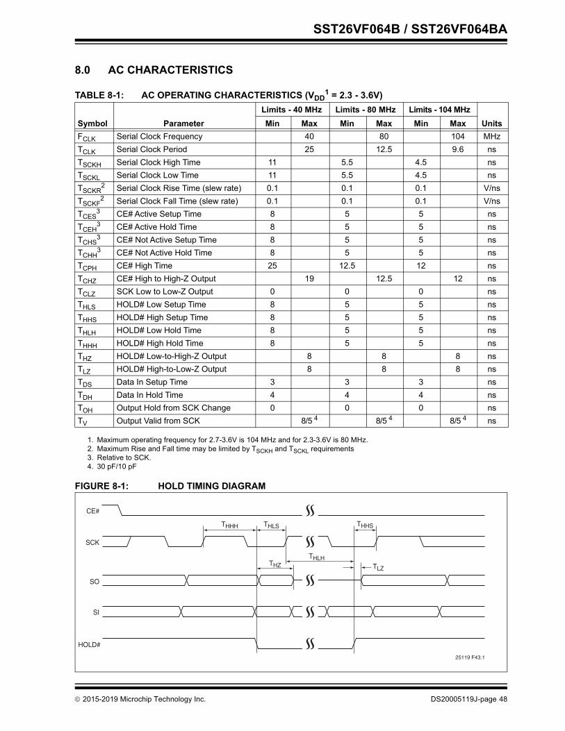
SST26VF064B / SST26VF064BA
8.0 AC CHARACTERISTICS
FIGURE 8-1: HOLD TIMING DIAGRAM
TABLE 8-1: AC OPERATING CHARACTERISTICS (VDD1 = 2.3 - 3.6V)
1. Maximum operating frequency for 2.7-3.6V is 104 MHz and for 2.3-3.6V is 80 MHz.
Symbol ParameterLimits - 40 MHz Limits - 80 MHz Limits - 104 MHz
UnitsMin Max Min Max Min MaxFCLK Serial Clock Frequency 40 80 104 MHzTCLK Serial Clock Period 25 12.5 9.6 nsTSCKH Serial Clock High Time 11 5.5 4.5 nsTSCKL Serial Clock Low Time 11 5.5 4.5 nsTSCKR
2
2. Maximum Rise and Fall time may be limited by TSCKH and TSCKL requirements
Serial Clock Rise Time (slew rate) 0.1 0.1 0.1 V/nsTSCKF
2 Serial Clock Fall Time (slew rate) 0.1 0.1 0.1 V/nsTCES
3
3. Relative to SCK.
CE# Active Setup Time 8 5 5 nsTCEH
3 CE# Active Hold Time 8 5 5 nsTCHS
3 CE# Not Active Setup Time 8 5 5 nsTCHH
3 CE# Not Active Hold Time 8 5 5 nsTCPH CE# High Time 25 12.5 12 nsTCHZ CE# High to High-Z Output 19 12.5 12 nsTCLZ SCK Low to Low-Z Output 0 0 0 nsTHLS HOLD# Low Setup Time 8 5 5 nsTHHS HOLD# High Setup Time 8 5 5 nsTHLH HOLD# Low Hold Time 8 5 5 nsTHHH HOLD# High Hold Time 8 5 5 nsTHZ HOLD# Low-to-High-Z Output 8 8 8 nsTLZ HOLD# High-to-Low-Z Output 8 8 8 nsTDS Data In Setup Time 3 3 3 nsTDH Data In Hold Time 4 4 4 nsTOH Output Hold from SCK Change 0 0 0 nsTV Output Valid from SCK 8/5 4
4. 30 pF/10 pF
8/5 4 8/5 4 ns
THZ TLZ
THHH THLS THHS
25119 F43.1
HOLD#
CE#
SCK
SO
SI
THLH
2015-2019 Microchip Technology Inc. DS20005119J-page 48
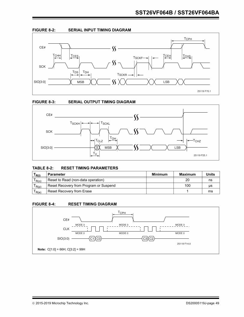
SST26VF064B / SST26VF064BA
FIGURE 8-2: SERIAL INPUT TIMING DIAGRAM
FIGURE 8-3: SERIAL OUTPUT TIMING DIAGRAM
FIGURE 8-4: RESET TIMING DIAGRAM
TABLE 8-2: RESET TIMING PARAMETERSTR(i) Parameter Minimum Maximum UnitsTR(o) Reset to Read (non-data operation) 20 nsTR(p) Reset Recovery from Program or Suspend 100 µsTR(e) Reset Recovery from Erase 1 ms
CE#
SIO[3:0]
SCK
MSB LSB
TDS TDH
TCHH TCES TCEH TCHS
TSCKR
TSCKF
TCPH
25119 F70.1
25119 F25.1
CE#
SIO[3:0]
SCK
MSB
TCLZ
TV
TSCKH
TCHZTOH
TSCKL
LSB
25119 F14.0
MODE 3
CLK
SIO(3:0)
CE#
MODE 3
C1 C3 C2C0
MODE 0
MODE 3
MODE 0MODE 0
TCPH
Note: C[1:0] = 66H; C[3:2] = 99H
2015-2019 Microchip Technology Inc. DS20005119J-page 49
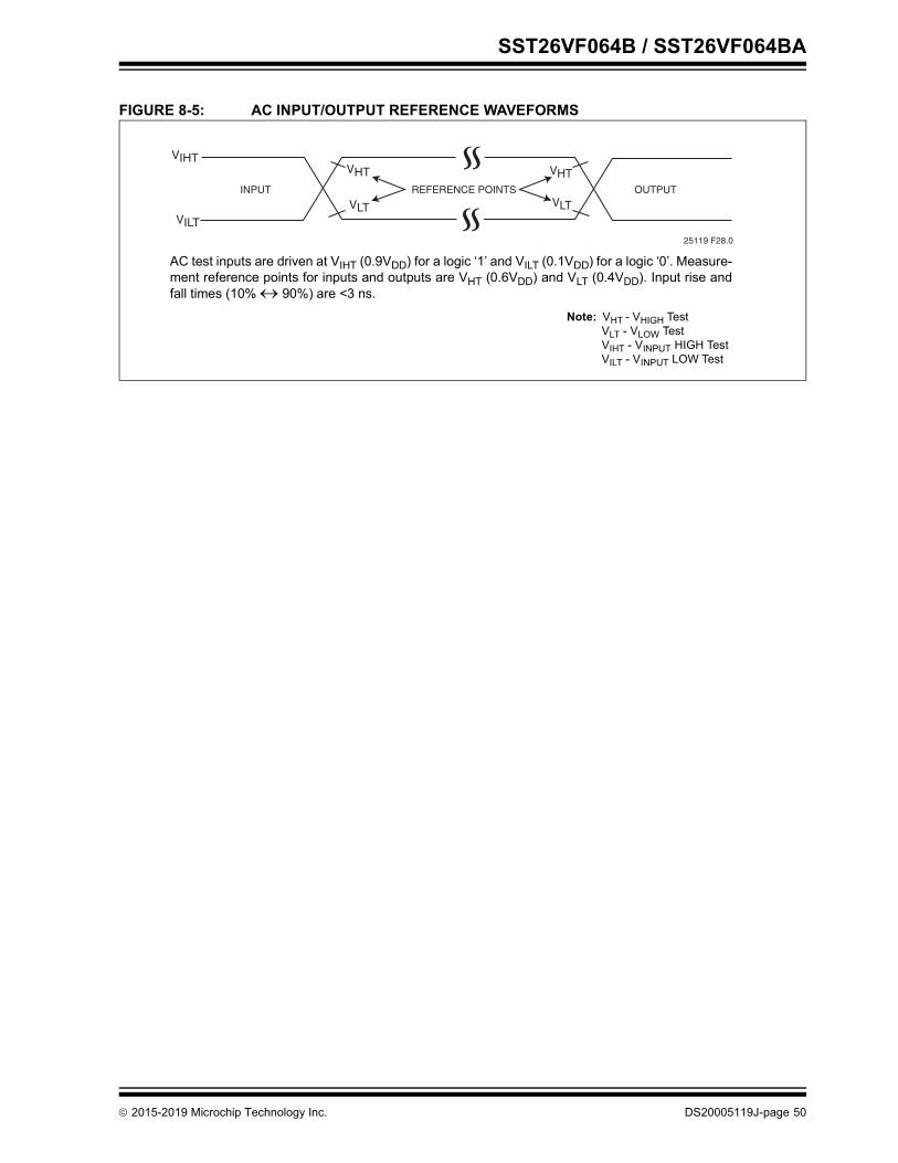
SST26VF064B / SST26VF064BA
FIGURE 8-5: AC INPUT/OUTPUT REFERENCE WAVEFORMS
25119 F28.0
REFERENCE POINTS OUTPUTINPUT
VHT
VLT
VHT
VLT
VIHT
VILT
AC test inputs are driven at VIHT (0.9VDD) for a logic ‘1’ and VILT (0.1VDD) for a logic ‘0’. Measure-ment reference points for inputs and outputs are VHT (0.6VDD) and VLT (0.4VDD). Input rise andfall times (10% 90%) are <3 ns.
Note: VHT - VHIGH TestVLT - VLOW TestVIHT - VINPUT HIGH TestVILT - VINPUT LOW Test
2015-2019 Microchip Technology Inc. DS20005119J-page 50
SST26VF064B / SST26VF064BA
9.0 PACKAGING INFORMATION9.1 Package Marking
8-Lead SOIJ (5.28 mm) Example
26F064BSM 3e
1506343
XXXXXXXXYYWWNNN
XXXXXXXXMF1506343
26F064Be3
8-Lead WDFN (5x6 mm) Example
24-Ball TBGA (6x8 mm) Example
YYWWNNNXXXXXXXXXXXXXXXXXXXXXXXXXXXXXX
1506343MN26F064B
e3
8-Lead WDFN (6x8 mm) Example
16-Lead SOIC (7.50 mm) Example
26F064BSO
15063433e
YYWWNNNXXXXXXXXXXXXXXXXXXXXXXXXXXXXXX
1506343TD26F064B
e3
Continued
2015-2019 Microchip Technology Inc. DS20005119J-page 51
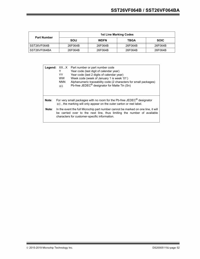
SST26VF064B / SST26VF064BA
Legend: XX...X Part number or part number codeY Year code (last digit of calendar year)YY Year code (last 2 digits of calendar year)WW Week code (week of January 1 is week ‘01’)NNN Alphanumeric traceability code (2 characters for small packages)
Pb-free JEDEC® designator for Matte Tin (Sn)
Note: For very small packages with no room for the Pb-free JEDEC® designator , the marking will only appear on the outer carton or reel label.
Note: In the event the full Microchip part number cannot be marked on one line, it willbe carried over to the next line, thus limiting the number of availablecharacters for customer-specific information.
3e
3e
Part Number1st Line Marking Codes
SOIJ WDFN TBGA SOICSST26VF064B 26F064B 26F064B 26F064B 26F064BSST26VF064BA 26F064B 26F064B 26F064B 26F064B
2015-2019 Microchip Technology Inc. DS20005119J-page 52
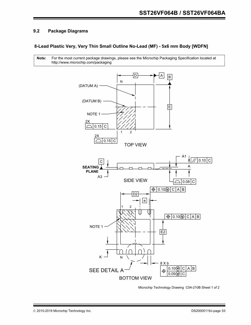
SST26VF064B / SST26VF064BA
9.2 Package Diagrams
BA
0.15 C
0.15 C
D2
E2
8 X b0.10 C A B0.05 C
(DATUM B)
(DATUM A)
CSEATING
PLANE
NOTE 1
2X
BOTTOM VIEW
Microchip Technology Drawing C04-210B Sheet 1 of 2
For the most current package drawings, please see the Microchip Packaging Specification located athttp://www.microchip.com/packaging
Note:
N
0.10 C A B
0.10 C A B
A3
0.10 C
0.08 C
A1
D
E
NOTE 1
2X
A
1 2
1 2
e
SEE DETAIL A
SIDE VIEW
TOP VIEW
N
K
8-Lead Plastic Very, Very Thin Small Outline No-Lead (MF) - 5x6 mm Body [WDFN]
2015-2019 Microchip Technology Inc. DS20005119J-page 53
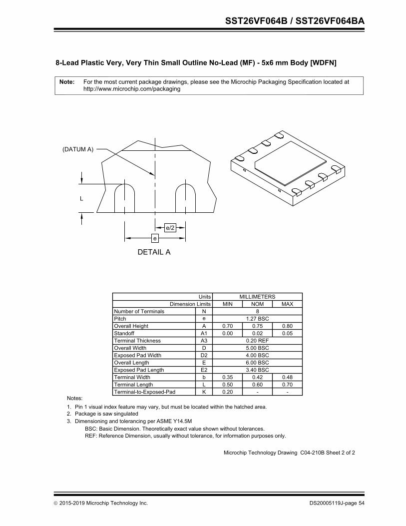
SST26VF064B / SST26VF064BA
Microchip Technology Drawing C04-210B Sheet 2 of 2
For the most current package drawings, please see the Microchip Packaging Specification located athttp://www.microchip.com/packaging
Note:
e/2
e
L
(DATUM A)
DETAIL A
8-Lead Plastic Very, Very Thin Small Outline No-Lead (MF) - 5x6 mm Body [WDFN]
Number of Terminals
Overall Height
Terminal Width
Overall Width
Overall Length
Terminal Length
Exposed Pad Width
Exposed Pad Length
Terminal Thickness
Pitch
Standoff
UnitsDimension Limits
A1A
b
ED2
E2
A3
e
L
D
N1.27 BSC
0.20 REF
0.500.35
0.700.00
0.42
6.00 BSC
0.60
3.40 BSC
4.00 BSC
0.750.02
5.00 BSC
MILLIMETERSMIN NOM
8
0.700.48
0.800.05
MAX
K -0.20 -
REF: Reference Dimension, usually without tolerance, for information purposes only.BSC: Basic Dimension. Theoretically exact value shown without tolerances.
1.2.3.
Notes:
Pin 1 visual index feature may vary, but must be located within the hatched area.Package is saw singulatedDimensioning and tolerancing per ASME Y14.5M
Terminal-to-Exposed-Pad
2015-2019 Microchip Technology Inc. DS20005119J-page 54
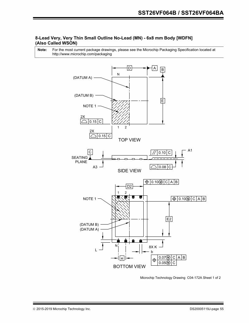
SST26VF064B / SST26VF064BA
A
0.15 C
0.15 C
0.07 C A B0.05 C
(DATUM B)
(DATUM A)
CSEATING
PLANE
NOTE 1
1 2
N
2X
TOP VIEW
SIDE VIEW
BOTTOM VIEW
Microchip Technology Drawing C04-172A Sheet 1 of 2
For the most current package drawings, please see the Microchip Packaging Specification located athttp://www.microchip.com/packaging
Note:
1 2
N
0.10 C A B
0.10 C A B
0.10 C
0.08 C
D
E
B
b
E2
D2
e
A3
A1
2X
L8X K
(DATUM B)(DATUM A)
8-Lead Very, Very Thin Small Outline No-Lead (MN) - 6x8 mm Body [WDFN](Also Called WSON)
NOTE 1
2015-2019 Microchip Technology Inc. DS20005119J-page 55
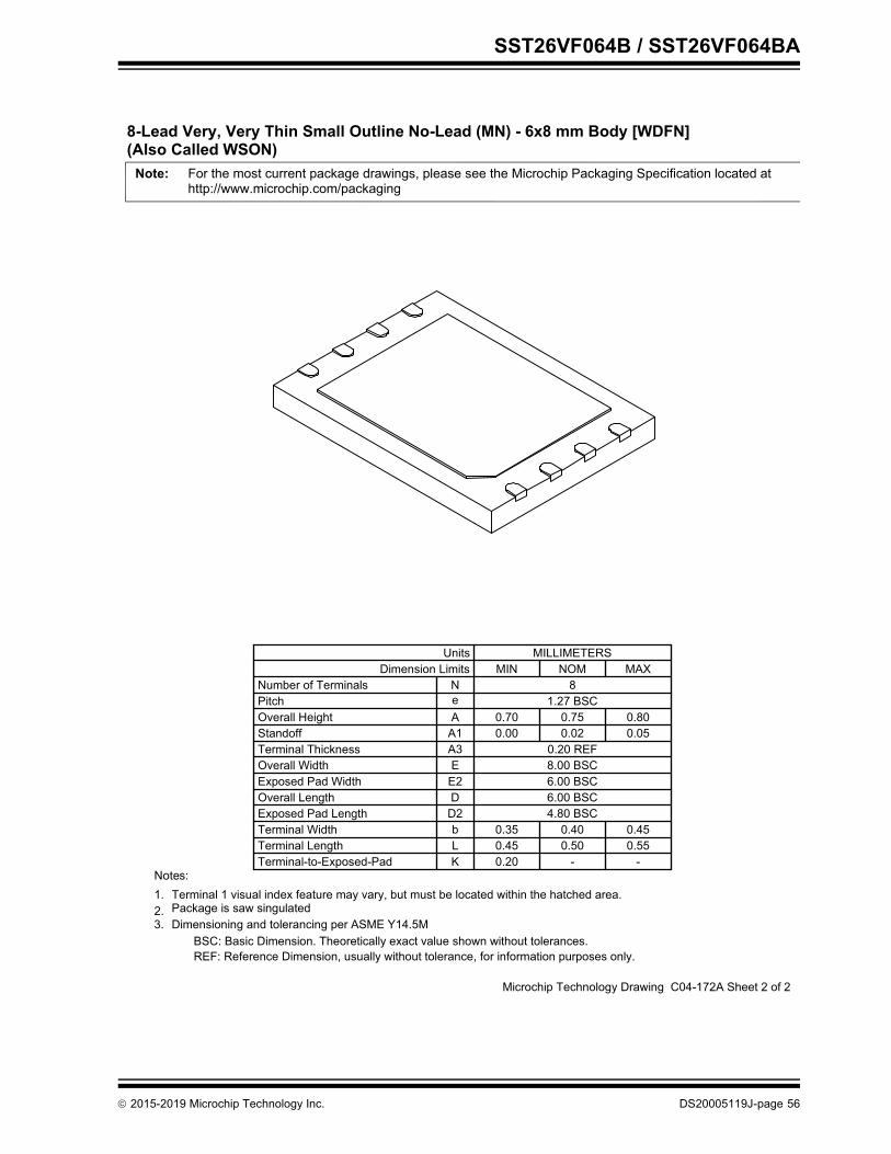
SST26VF064B / SST26VF064BA
Microchip Technology Drawing C04-172A Sheet 2 of 2
For the most current package drawings, please see the Microchip Packaging Specification located athttp://www.microchip.com/packaging
Note:
8-Lead Very, Very Thin Small Outline No-Lead (MN) - 6x8 mm Body [WDFN]
Number of Terminals
Overall Height
Terminal Width
Overall Width
Overall Length
Terminal Length
Exposed Pad Width
Exposed Pad Length
Terminal Thickness
Pitch
Standoff
UnitsDimension Limits
A1A
b
DE2
D2
A3
e
L
E
N1.27 BSC
0.20 REF
0.450.35
0.700.00
0.40
6.00 BSC
0.50
4.80 BSC
6.00 BSC
0.750.02
8.00 BSC
MILLIMETERSMIN NOM
8
0.550.45
0.800.05
MAX
K -0.20 -
REF: Reference Dimension, usually without tolerance, for information purposes only.BSC: Basic Dimension. Theoretically exact value shown without tolerances.
1.
3.
Notes:
Package is saw singulatedDimensioning and tolerancing per ASME Y14.5M
Terminal-to-Exposed-Pad
(Also Called WSON)
2.Terminal 1 visual index feature may vary, but must be located within the hatched area.
2015-2019 Microchip Technology Inc. DS20005119J-page 56
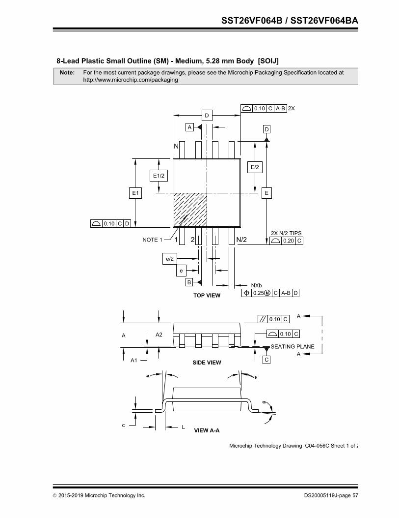
SST26VF064B / SST26VF064BA
Note: For the most current package drawings, please see the Microchip Packaging Specification located at http://www.microchip.com/packaging
2015-2019 Microchip Technology Inc. DS20005119J-page 57
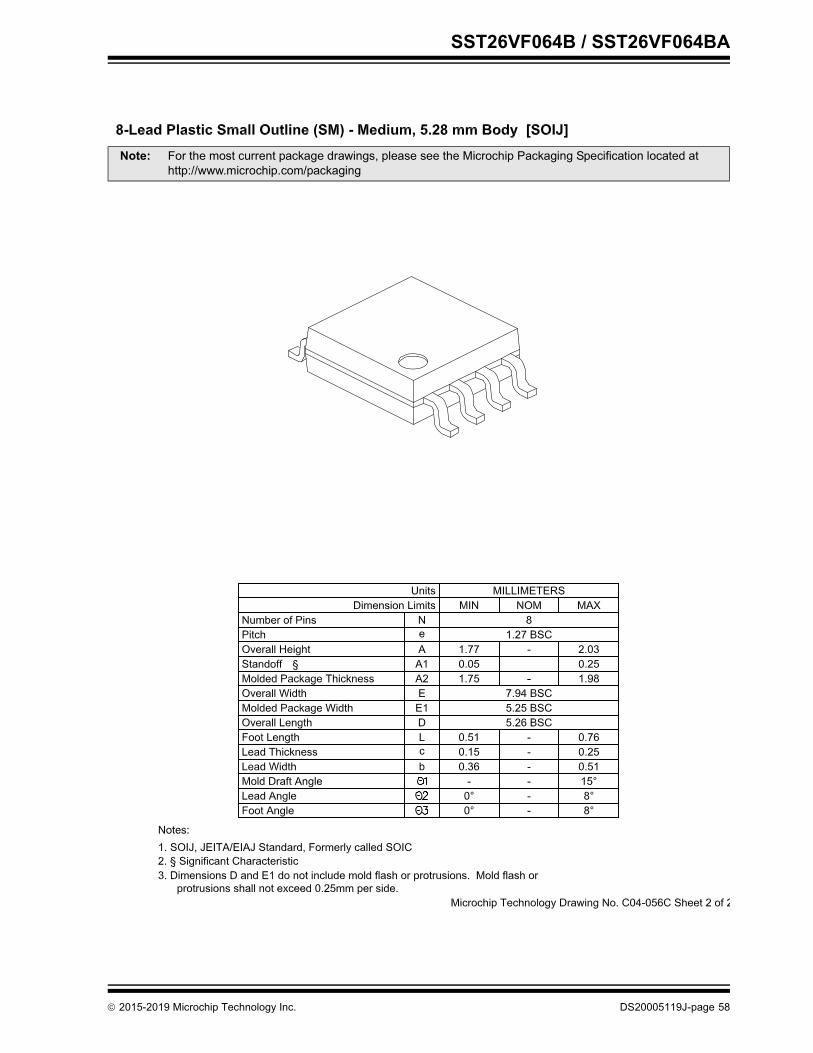
SST26VF064B / SST26VF064BA
Note: For the most current package drawings, please see the Microchip Packaging Specification located at http://www.microchip.com/packaging
2015-2019 Microchip Technology Inc. DS20005119J-page 58
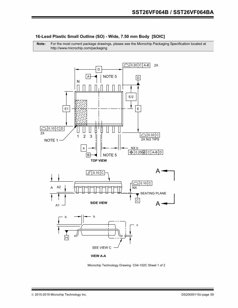
SST26VF064B / SST26VF064BA
Note: For the most current package drawings, please see the Microchip Packaging Specification located at http://www.microchip.com/packaging
2015-2019 Microchip Technology Inc. DS20005119J-page 59
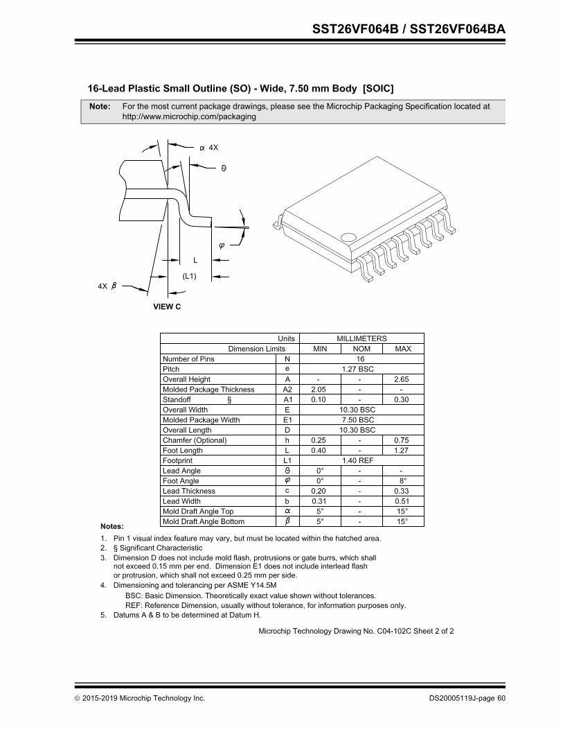
SST26VF064B / SST26VF064BA
Note: For the most current package drawings, please see the Microchip Packaging Specification located at http://www.microchip.com/packaging
2015-2019 Microchip Technology Inc. DS20005119J-page 60
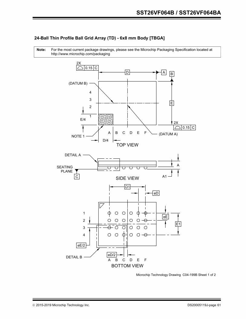
SST26VF064B / SST26VF064BA
Note:
24-Ball Thin Profile Ball Grid Array (TD) - 6x8 mm Body [TBGA]
2015-2019 Microchip Technology Inc. DS20005119J-page 61
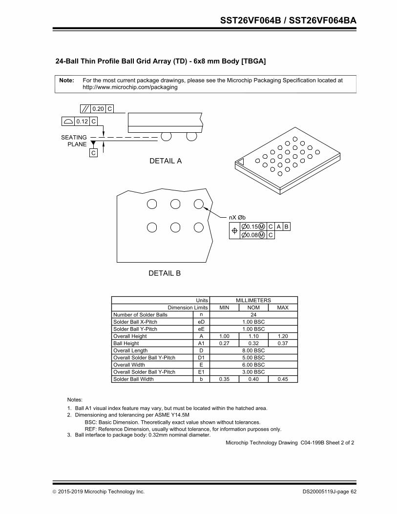
SST26VF064B / SST26VF064BA
Note:
24-Ball Thin Profile Ball Grid Array (TD) - 6x8 mm Body [TBGA]
Notes:
2015-2019 Microchip Technology Inc. DS20005119J-page 62
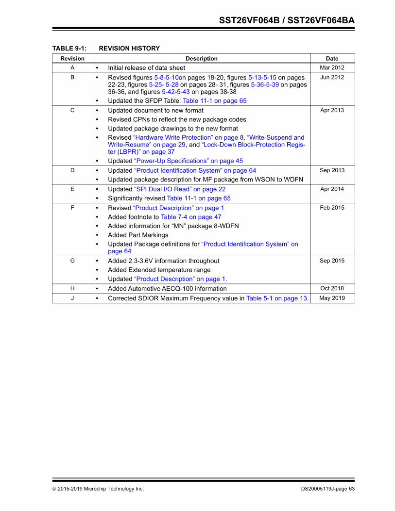
SST26VF064B / SST26VF064BA
TABLE 9-1: REVISION HISTORYRevision Description Date
A • Initial release of data sheet Mar 2012B • Revised figures 5-8-5-10on pages 18-20, figures 5-13-5-15 on pages
22-23, figures 5-25- 5-28 on pages 28- 31, figures 5-36-5-39 on pages 36-36, and figures 5-42-5-43 on pages 38-38
• Updated the SFDP Table: Table 11-1 on page 65
Jun 2012
C • Updated document to new format• Revised CPNs to reflect the new package codes• Updated package drawings to the new format• Revised “Hardware Write Protection” on page 8, “Write-Suspend and
Write-Resume” on page 29, and “Lock-Down Block-Protection Regis-ter (LBPR)” on page 37
• Updated “Power-Up Specifications” on page 45
Apr 2013
D • Updated “Product Identification System” on page 64• Updated package description for MF package from WSON to WDFN
Sep 2013
E • Updated “SPI Dual I/O Read” on page 22• Significantly revised Table 11-1 on page 65
Apr 2014
F • Revised “Product Description” on page 1• Added footnote to Table 7-4 on page 47• Added information for “MN” package 8-WDFN• Added Part Markings• Updated Package definitions for “Product Identification System” on
page 64
Feb 2015
G • Added 2.3-3.6V information throughout• Added Extended temperature range• Updated “Product Description” on page 1.
Sep 2015
H • Added Automotive AECQ-100 information Oct 2018J • Corrected SDIOR Maximum Frequency value in Table 5-1 on page 13. May 2019
2015-2019 Microchip Technology Inc. DS20005119J-page 63
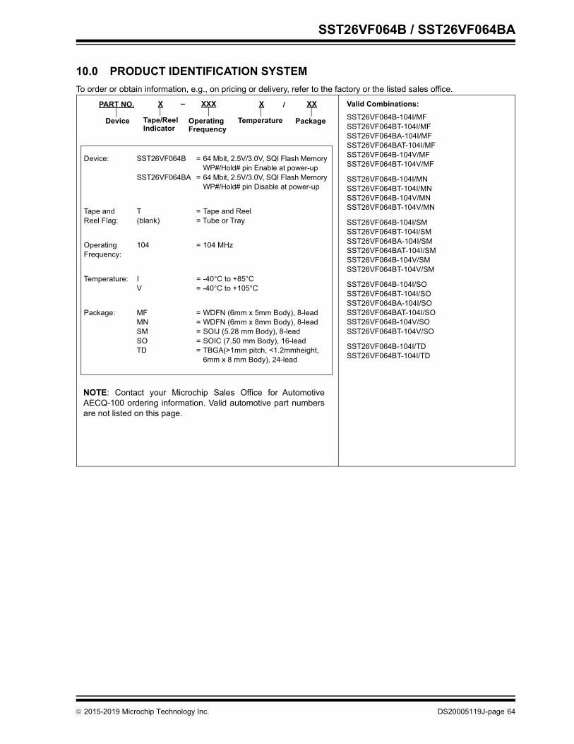
SST26VF064B / SST26VF064BA
10.0 PRODUCT IDENTIFICATION SYSTEMTo order or obtain information, e.g., on pricing or delivery, refer to the factory or the listed sales office.
PART NO. XXX X
TemperatureOperating Device
Device: SST26VF064B = 64 Mbit, 2.5V/3.0V, SQI Flash Memory
WP#/Hold# pin Enable at power-upSST26VF064BA = 64 Mbit, 2.5V/3.0V, SQI Flash Memory
WP#/Hold# pin Disable at power-up
Tape and Reel Flag:
T = Tape and Reel(blank) = Tube or Tray
Operating Frequency:
104 = 104 MHz
Temperature: I = -40°C to +85°CV = -40°C to +105°C
Package: MF = WDFN (6mm x 5mm Body), 8-leadMN = WDFN (6mm x 8mm Body), 8-leadSM = SOIJ (5.28 mm Body), 8-leadSO = SOIC (7.50 mm Body), 16-leadTD = TBGA(>1mm pitch, <1.2mmheight,
6mm x 8 mm Body), 24-lead
Valid Combinations:SST26VF064B-104I/MFSST26VF064BT-104I/MFSST26VF064BA-104I/MFSST26VF064BAT-104I/MFSST26VF064B-104V/MFSST26VF064BT-104V/MF
SST26VF064B-104I/MNSST26VF064BT-104I/MNSST26VF064B-104V/MNSST26VF064BT-104V/MN
SST26VF064B-104I/SM SST26VF064BT-104I/SM SST26VF064BA-104I/SMSST26VF064BAT-104I/SMSST26VF064B-104V/SM SST26VF064BT-104V/SM
SST26VF064B-104I/SO SST26VF064BT-104I/SO SST26VF064BA-104I/SOSST26VF064BAT-104I/SOSST26VF064B-104V/SO SST26VF064BT-104V/SO
SST26VF064B-104I/TDSST26VF064BT-104I/TD
X
Tape/ReelIndicator Frequency
XX
Package
/–
NOTE: Contact your Microchip Sales Office for AutomotiveAECQ-100 ordering information. Valid automotive part numbersare not listed on this page.
2015-2019 Microchip Technology Inc. DS20005119J-page 64
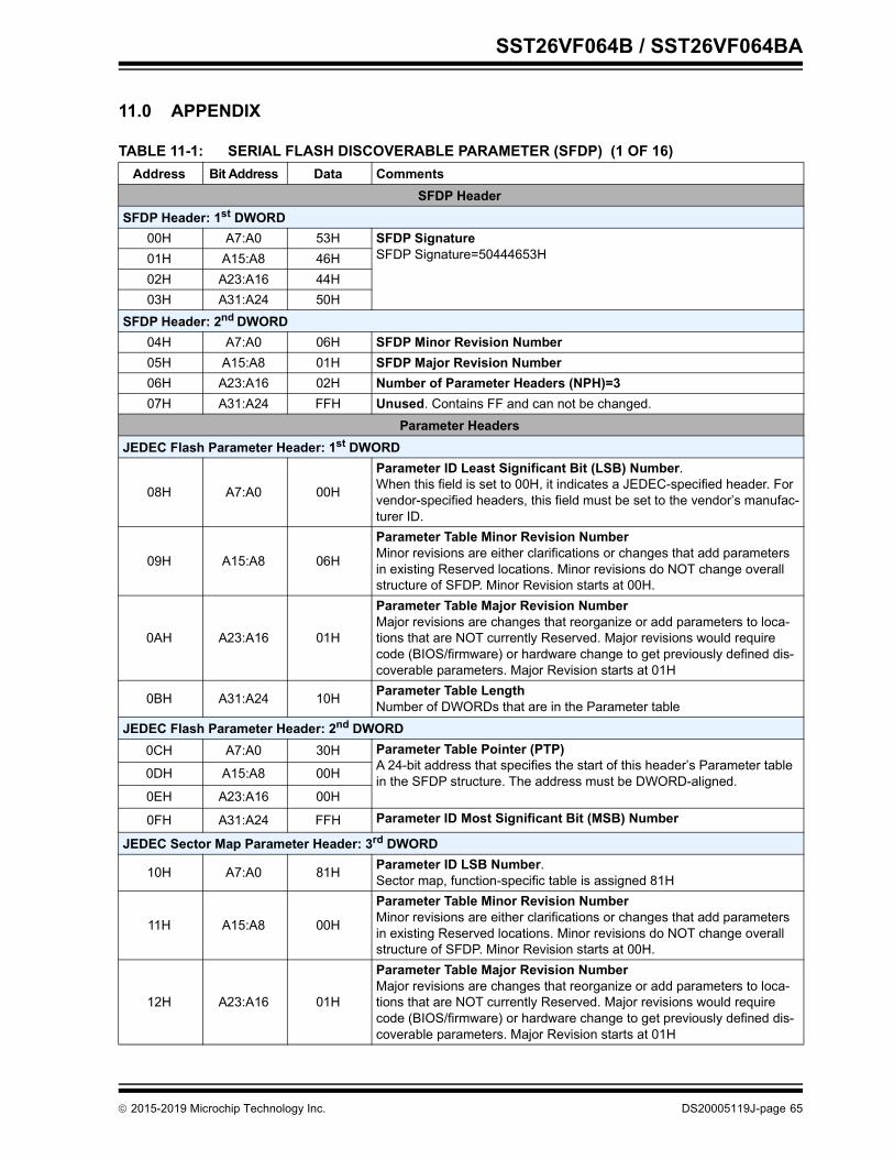
SST26VF064B / SST26VF064BA
11.0 APPENDIX
TABLE 11-1: SERIAL FLASH DISCOVERABLE PARAMETER (SFDP) (1 OF 16)Address Bit Address Data Comments
SFDP HeaderSFDP Header: 1st DWORD
00H A7:A0 53H SFDP SignatureSFDP Signature=50444653H01H A15:A8 46H
02H A23:A16 44H03H A31:A24 50H
SFDP Header: 2nd DWORD04H A7:A0 06H SFDP Minor Revision Number05H A15:A8 01H SFDP Major Revision Number06H A23:A16 02H Number of Parameter Headers (NPH)=307H A31:A24 FFH Unused. Contains FF and can not be changed.
Parameter HeadersJEDEC Flash Parameter Header: 1st DWORD
08H A7:A0 00H
Parameter ID Least Significant Bit (LSB) Number.When this field is set to 00H, it indicates a JEDEC-specified header. For vendor-specified headers, this field must be set to the vendor’s manufac-turer ID.
09H A15:A8 06H
Parameter Table Minor Revision NumberMinor revisions are either clarifications or changes that add parameters in existing Reserved locations. Minor revisions do NOT change overall structure of SFDP. Minor Revision starts at 00H.
0AH A23:A16 01H
Parameter Table Major Revision NumberMajor revisions are changes that reorganize or add parameters to loca-tions that are NOT currently Reserved. Major revisions would require code (BIOS/firmware) or hardware change to get previously defined dis-coverable parameters. Major Revision starts at 01H
0BH A31:A24 10H Parameter Table LengthNumber of DWORDs that are in the Parameter table
JEDEC Flash Parameter Header: 2nd DWORD0CH A7:A0 30H Parameter Table Pointer (PTP)
A 24-bit address that specifies the start of this header’s Parameter table in the SFDP structure. The address must be DWORD-aligned.0DH A15:A8 00H
0EH A23:A16 00H
0FH A31:A24 FFH Parameter ID Most Significant Bit (MSB) Number
JEDEC Sector Map Parameter Header: 3rd DWORD
10H A7:A0 81H Parameter ID LSB Number.Sector map, function-specific table is assigned 81H
11H A15:A8 00H
Parameter Table Minor Revision NumberMinor revisions are either clarifications or changes that add parameters in existing Reserved locations. Minor revisions do NOT change overall structure of SFDP. Minor Revision starts at 00H.
12H A23:A16 01H
Parameter Table Major Revision NumberMajor revisions are changes that reorganize or add parameters to loca-tions that are NOT currently Reserved. Major revisions would require code (BIOS/firmware) or hardware change to get previously defined dis-coverable parameters. Major Revision starts at 01H
2015-2019 Microchip Technology Inc. DS20005119J-page 65
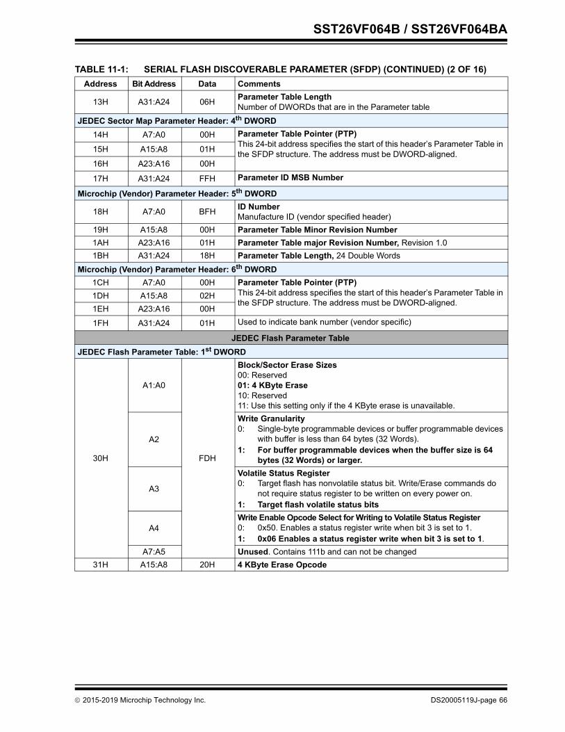
SST26VF064B / SST26VF064BA
13H A31:A24 06H Parameter Table LengthNumber of DWORDs that are in the Parameter table
JEDEC Sector Map Parameter Header: 4th DWORD14H A7:A0 00H Parameter Table Pointer (PTP)
This 24-bit address specifies the start of this header’s Parameter Table in the SFDP structure. The address must be DWORD-aligned.15H A15:A8 01H
16H A23:A16 00H
17H A31:A24 FFH Parameter ID MSB Number
Microchip (Vendor) Parameter Header: 5th DWORD
18H A7:A0 BFH ID NumberManufacture ID (vendor specified header)
19H A15:A8 00H Parameter Table Minor Revision Number1AH A23:A16 01H Parameter Table major Revision Number, Revision 1.01BH A31:A24 18H Parameter Table Length, 24 Double Words
Microchip (Vendor) Parameter Header: 6th DWORD1CH A7:A0 00H Parameter Table Pointer (PTP)
This 24-bit address specifies the start of this header’s Parameter Table in the SFDP structure. The address must be DWORD-aligned.
1DH A15:A8 02H1EH A23:A16 00H
1FH A31:A24 01H Used to indicate bank number (vendor specific)
JEDEC Flash Parameter TableJEDEC Flash Parameter Table: 1st DWORD
30H
A1:A0
FDH
Block/Sector Erase Sizes00: Reserved01: 4 KByte Erase10: Reserved11: Use this setting only if the 4 KByte erase is unavailable.
A2
Write Granularity0: Single-byte programmable devices or buffer programmable devices
with buffer is less than 64 bytes (32 Words).1: For buffer programmable devices when the buffer size is 64
bytes (32 Words) or larger.
A3
Volatile Status Register0: Target flash has nonvolatile status bit. Write/Erase commands do
not require status register to be written on every power on.1: Target flash volatile status bits
A4Write Enable Opcode Select for Writing to Volatile Status Register0: 0x50. Enables a status register write when bit 3 is set to 1.1: 0x06 Enables a status register write when bit 3 is set to 1.
A7:A5 Unused. Contains 111b and can not be changed31H A15:A8 20H 4 KByte Erase Opcode
TABLE 11-1: SERIAL FLASH DISCOVERABLE PARAMETER (SFDP) (CONTINUED) (2 OF 16)Address Bit Address Data Comments
2015-2019 Microchip Technology Inc. DS20005119J-page 66
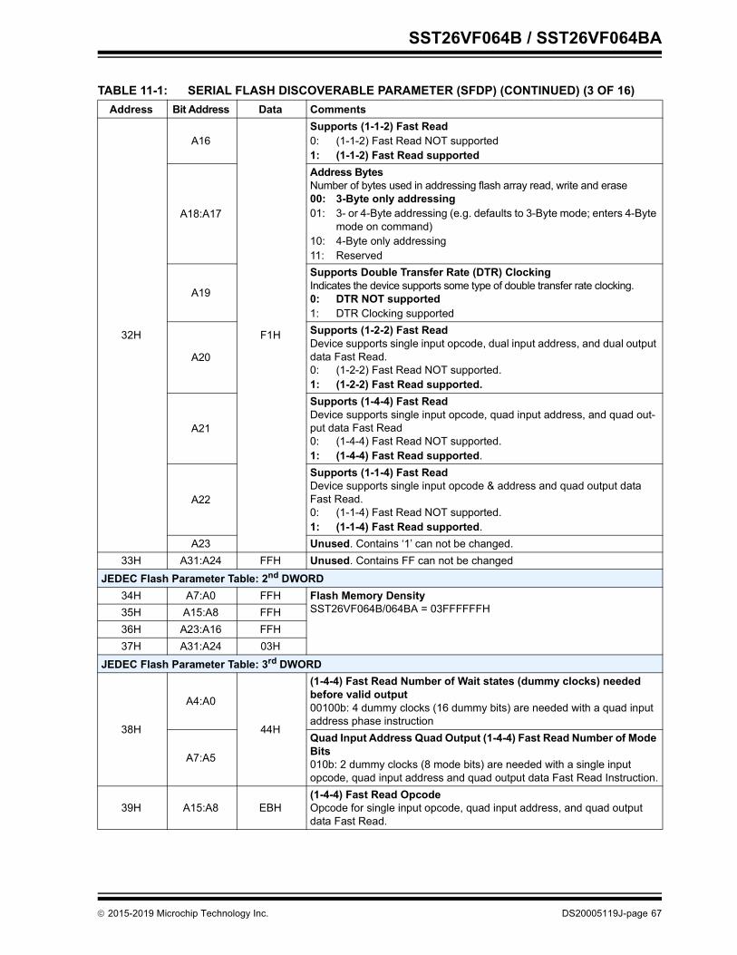
SST26VF064B / SST26VF064BA
32H
A16
F1H
Supports (1-1-2) Fast Read0: (1-1-2) Fast Read NOT supported1: (1-1-2) Fast Read supported
A18:A17
Address BytesNumber of bytes used in addressing flash array read, write and erase00: 3-Byte only addressing01: 3- or 4-Byte addressing (e.g. defaults to 3-Byte mode; enters 4-Byte
mode on command)10: 4-Byte only addressing11: Reserved
A19
Supports Double Transfer Rate (DTR) ClockingIndicates the device supports some type of double transfer rate clocking.0: DTR NOT supported1: DTR Clocking supported
A20
Supports (1-2-2) Fast ReadDevice supports single input opcode, dual input address, and dual output data Fast Read.0: (1-2-2) Fast Read NOT supported.1: (1-2-2) Fast Read supported.
A21
Supports (1-4-4) Fast ReadDevice supports single input opcode, quad input address, and quad out-put data Fast Read0: (1-4-4) Fast Read NOT supported.1: (1-4-4) Fast Read supported.
A22
Supports (1-1-4) Fast ReadDevice supports single input opcode & address and quad output data Fast Read.0: (1-1-4) Fast Read NOT supported.1: (1-1-4) Fast Read supported.
A23 Unused. Contains ‘1’ can not be changed.33H A31:A24 FFH Unused. Contains FF can not be changed
JEDEC Flash Parameter Table: 2nd DWORD34H A7:A0 FFH Flash Memory Density
SST26VF064B/064BA = 03FFFFFFH35H A15:A8 FFH36H A23:A16 FFH37H A31:A24 03H
JEDEC Flash Parameter Table: 3rd DWORD
38H
A4:A0
44H
(1-4-4) Fast Read Number of Wait states (dummy clocks) needed before valid output00100b: 4 dummy clocks (16 dummy bits) are needed with a quad input address phase instruction
A7:A5
Quad Input Address Quad Output (1-4-4) Fast Read Number of Mode Bits010b: 2 dummy clocks (8 mode bits) are needed with a single input opcode, quad input address and quad output data Fast Read Instruction.
39H A15:A8 EBH(1-4-4) Fast Read OpcodeOpcode for single input opcode, quad input address, and quad output data Fast Read.
TABLE 11-1: SERIAL FLASH DISCOVERABLE PARAMETER (SFDP) (CONTINUED) (3 OF 16)Address Bit Address Data Comments
2015-2019 Microchip Technology Inc. DS20005119J-page 67
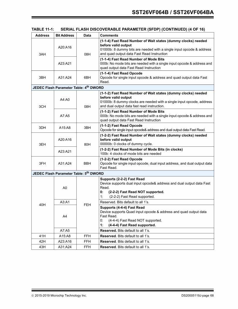
SST26VF064B / SST26VF064BA
3AH
A20:A16
08H
(1-1-4) Fast Read Number of Wait states (dummy clocks) needed before valid output01000b: 8 dummy bits are needed with a single input opcode & address and quad output data Fast Read Instruction
A23:A21(1-1-4) Fast Read Number of Mode Bits000b: No mode bits are needed with a single input opcode & address and quad output data Fast Read Instruction
3BH A31:A24 6BH(1-1-4) Fast Read OpcodeOpcode for single input opcode & address and quad output data Fast Read.
JEDEC Flash Parameter Table: 4th DWORD
3CH
A4:A0
08H
(1-1-2) Fast Read Number of Wait states (dummy clocks) needed before valid output 01000b: 8 dummy clocks are needed with a single input opcode, address and dual output data fast read instruction.
A7:A5(1-1-2) Fast Read Number of Mode Bits000b: No mode bits are needed with a single input opcode & address and quad output data Fast Read Instruction
3DH A15:A8 3BH (1-1-2) Fast Read OpcodeOpcode for single input opcode& address and dual output data Fast Read.
3EHA20:A16
80H
(1-2-2) Fast Read Number of Wait states (dummy clocks) needed before valid output00000b: 0 clocks of dummy cycle.
A23:A21 (1-2-2) Fast Read Number of Mode Bits (in clocks)100b: 4 clocks of mode bits are needed
3FH A31:A24 BBH(1-2-2) Fast Read OpcodeOpcode for single input opcode, dual input address, and dual output data Fast Read.
JEDEC Flash Parameter Table: 5th DWORD
40H
A0
FEH
Supports (2-2-2) Fast ReadDevice supports dual input opcode& address and dual output data Fast Read.0: (2-2-2) Fast Read NOT supported.1: (2-2-2) Fast Read supported.
A3:A1 Reserved. Bits default to all 1’s.
A4
Supports (4-4-4) Fast ReadDevice supports Quad input opcode & address and quad output data Fast Read.0: (4-4-4) Fast Read NOT supported.1: (4-4-4) Fast Read supported.
A7:A5 Reserved. Bits default to all 1’s.41H A15:A8 FFH Reserved. Bits default to all 1’s.42H A23:A16 FFH Reserved. Bits default to all 1’s.43H A31:A24 FFH Reserved. Bits default to all 1’s.
TABLE 11-1: SERIAL FLASH DISCOVERABLE PARAMETER (SFDP) (CONTINUED) (4 OF 16)Address Bit Address Data Comments
2015-2019 Microchip Technology Inc. DS20005119J-page 68
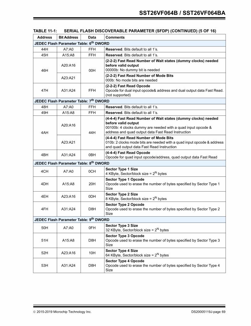
SST26VF064B / SST26VF064BA
JEDEC Flash Parameter Table: 6th DWORD44H A7:A0 FFH Reserved. Bits default to all 1’s.45H A15:A8 FFH Reserved. Bits default to all 1’s.
46HA20:A16
00H
(2-2-2) Fast Read Number of Wait states (dummy clocks) needed before valid output00000b: No dummy bit is needed
A23:A21 (2-2-2) Fast Read Number of Mode Bits000b: No mode bits are needed
47H A31:A24 FFH(2-2-2) Fast Read OpcodeOpcode for dual input opcode& address and dual output data Fast Read. (not supported)
JEDEC Flash Parameter Table: 7th DWORD48H A7:A0 FFH Reserved. Bits default to all 1’s.49H A15:A8 FFH Reserved. Bits default to all 1’s.
4AH
A20:A16
44H
(4-4-4) Fast Read Number of Wait states (dummy clocks) needed before valid output00100b: 4 clocks dummy are needed with a quad input opcode & address and quad output data Fast Read Instruction
A23:A21(4-4-4) Fast Read Number of Mode Bits010b: 2 clocks mode bits are needed with a quad input opcode & address and quad output data Fast Read Instruction
4BH A31:A24 0BH (4-4-4) Fast Read OpcodeOpcode for quad input opcode/address, quad output data Fast Read
JEDEC Flash Parameter Table: 8th DWORD
4CH A7:A0 0CH Sector Type 1 Size4 KByte, Sector/block size = 2N bytes
4DH A15:A8 20HSector Type 1 OpcodeOpcode used to erase the number of bytes specified by Sector Type 1 Size
4EH A23:A16 0DH Sector Type 2 Size8 KByte, Sector/block size = 2N bytes
4FH A31:A24 D8HSector Type 2 OpcodeOpcode used to erase the number of bytes specified by Sector Type 2 Size
JEDEC Flash Parameter Table: 9th DWORD
50H A7:A0 0FH Sector Type 3 Size32 KByte, Sector/block size = 2N bytes
51H A15:A8 D8HSector Type 3 OpcodeOpcode used to erase the number of bytes specified by Sector Type 3 Size
52H A23:A16 10H Sector Type 4 Size64 KByte, Sector/block size = 2N bytes
53H A31:A24 D8HSector Type 4 OpcodeOpcode used to erase the number of bytes specified by Sector Type 4 Size
TABLE 11-1: SERIAL FLASH DISCOVERABLE PARAMETER (SFDP) (CONTINUED) (5 OF 16)Address Bit Address Data Comments
2015-2019 Microchip Technology Inc. DS20005119J-page 69
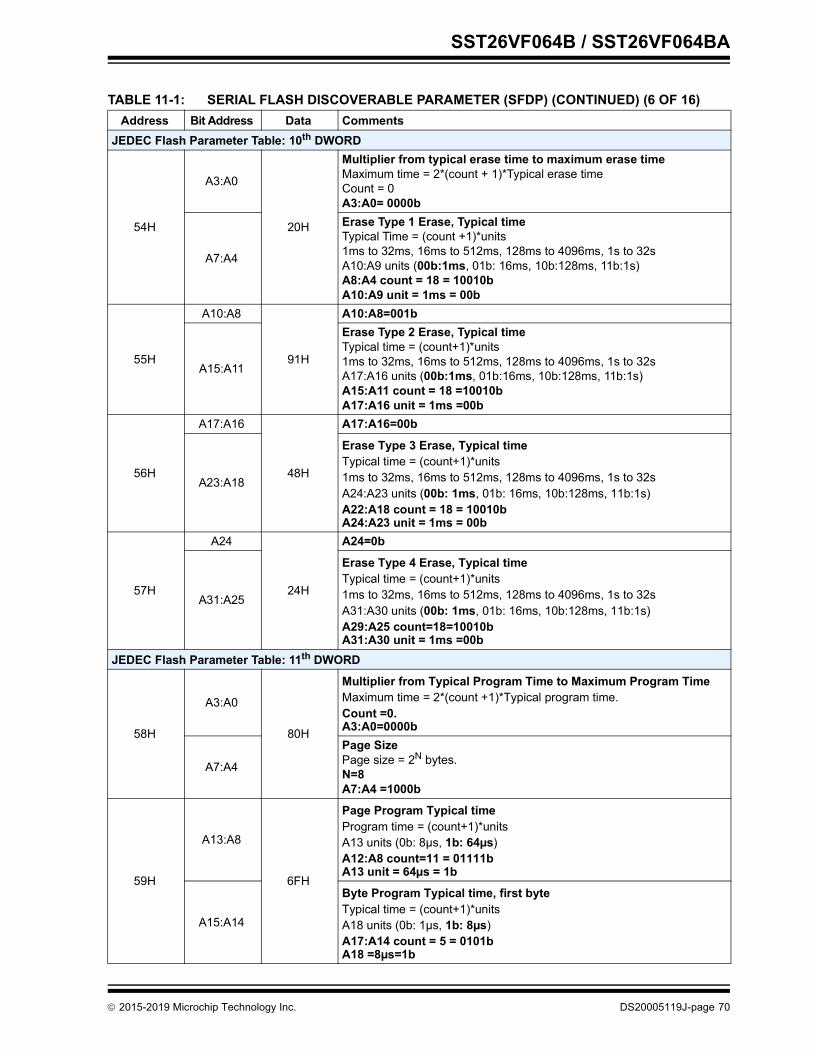
SST26VF064B / SST26VF064BA
JEDEC Flash Parameter Table: 10th DWORD
54H
A3:A0
20H
Multiplier from typical erase time to maximum erase timeMaximum time = 2*(count + 1)*Typical erase timeCount = 0 A3:A0= 0000b
A7:A4
Erase Type 1 Erase, Typical timeTypical Time = (count +1)*units1ms to 32ms, 16ms to 512ms, 128ms to 4096ms, 1s to 32sA10:A9 units (00b:1ms, 01b: 16ms, 10b:128ms, 11b:1s)A8:A4 count = 18 = 10010bA10:A9 unit = 1ms = 00b
55H
A10:A8
91H
A10:A8=001b
A15:A11
Erase Type 2 Erase, Typical timeTypical time = (count+1)*units1ms to 32ms, 16ms to 512ms, 128ms to 4096ms, 1s to 32sA17:A16 units (00b:1ms, 01b:16ms, 10b:128ms, 11b:1s)A15:A11 count = 18 =10010bA17:A16 unit = 1ms =00b
56H
A17:A16
48H
A17:A16=00b
A23:A18
Erase Type 3 Erase, Typical timeTypical time = (count+1)*units1ms to 32ms, 16ms to 512ms, 128ms to 4096ms, 1s to 32sA24:A23 units (00b: 1ms, 01b: 16ms, 10b:128ms, 11b:1s)A22:A18 count = 18 = 10010bA24:A23 unit = 1ms = 00b
57H
A24
24H
A24=0b
A31:A25
Erase Type 4 Erase, Typical timeTypical time = (count+1)*units1ms to 32ms, 16ms to 512ms, 128ms to 4096ms, 1s to 32sA31:A30 units (00b: 1ms, 01b: 16ms, 10b:128ms, 11b:1s)A29:A25 count=18=10010bA31:A30 unit = 1ms =00b
JEDEC Flash Parameter Table: 11th DWORD
58H
A3:A0
80H
Multiplier from Typical Program Time to Maximum Program TimeMaximum time = 2*(count +1)*Typical program time.Count =0.A3:A0=0000b
A7:A4
Page SizePage size = 2N bytes.N=8 A7:A4 =1000b
59H
A13:A8
6FH
Page Program Typical time Program time = (count+1)*unitsA13 units (0b: 8µs, 1b: 64µs)A12:A8 count=11 = 01111bA13 unit = 64µs = 1b
A15:A14
Byte Program Typical time, first byteTypical time = (count+1)*unitsA18 units (0b: 1µs, 1b: 8µs)A17:A14 count = 5 = 0101bA18 =8µs=1b
TABLE 11-1: SERIAL FLASH DISCOVERABLE PARAMETER (SFDP) (CONTINUED) (6 OF 16)Address Bit Address Data Comments
2015-2019 Microchip Technology Inc. DS20005119J-page 70
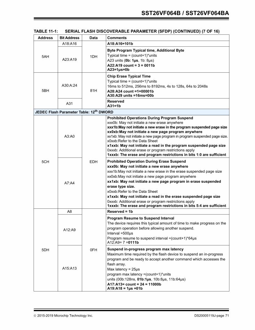
SST26VF064B / SST26VF064BA
5AH
A18:A16
1DH
A18:A16=101b
A23:A19
Byte Program Typical time, Additional ByteTypical time = (count+1)*unitsA23 units (0b: 1µs, 1b: 8µs)A22:A19 count = 3 = 0011bA23=1μs=0b
5BHA30:A:24
81H
Chip Erase Typical TimeTypical time = (count+1)*units16ms to 512ms, 256ms to 8192ms, 4s to 128s, 64s to 2048sA28:A24 count =1=00001bA30:A29 units =16ms=00b
A31 ReservedA31=1b
JEDEC Flash Parameter Table: 12th DWORD
5CH
A3:A0
EDH
Prohibited Operations During Program Suspendxxx0b: May not initiate a new erase anywherexxx1b:May not initiate a new erase in the program suspended page sizexx0xb:May not initiate a new page program anywherexx1xb: May not initiate a new page program in program suspended page size.x0xxb:Refer to the Data Sheetx1xxb: May not initiate a read in the program suspended page size0xxxb: Additional erase or program restrictions apply1xxxb: The erase and program restrictions in bits 1:0 are sufficient
A7:A4
Prohibited Operation During Erase Suspendxxx0b: May not initiate a new erase anywherexxx1b:May not initiate a new erase in the erase suspended page sizexx0xb:May not initiate a new page program anywherexx1xb: May not initiate a new page program in erase suspended erase type size.x0xxb:Refer to the Data Sheetx1xxb: May not initiate a read in the erase suspended page size0xxxb: Additional erase or program restrictions apply1xxxb: The erase and program restrictions in bits 5:4 are sufficient
5DH
A8
0FH
Reserved = 1b
A12:A9
Program Resume to Suspend IntervalThe device requires this typical amount of time to make progress on the program operation before allowing another suspend.Interval =500µsProgram resume to suspend interval =(count+1)*64µsA12:A9= 7 =0111b
A15:A13
Suspend in-progress program max latencyMaximum time required by the flash device to suspend an in-progress program and be ready to accept another command which accesses the flash array.Max latency = 25µsprogram max latency =(count+1)*unitsunits (00b:128ns, 01b:1µs, 10b:8µs, 11b:64µs)A17:A13= count = 24 = 11000bA19:A18 = 1µs =01b
TABLE 11-1: SERIAL FLASH DISCOVERABLE PARAMETER (SFDP) (CONTINUED) (7 OF 16)Address Bit Address Data Comments
2015-2019 Microchip Technology Inc. DS20005119J-page 71
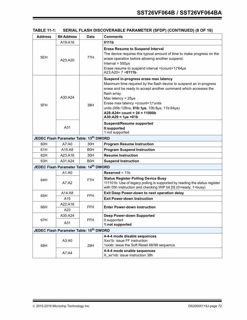
SST26VF064B / SST26VF064BA
5EH
A19:A16
77H
0111b
A23:A20
Erase Resume to Suspend IntervalThe device requires this typical amount of time to make progress on the erase operation before allowing another suspend.Interval = 500µsErase resume to suspend interval =(count+1)*64µsA23:A20= 7 =0111b
5FH
A30:A24
38H
Suspend in-progress erase max latencyMaximum time required by the flash device to suspend an in-progress erase and be ready to accept another command which accesses the flash array.Max latency = 25µsErase max latency =(count+1)*unitsunits (00b:128ns, 01b:1µs, 10b:8µs, 11b:64µs)A28:A24= count = 24 = 11000bA30:A29 = 1µs =01b
A31Suspend/Resume supported0:supported1:not supported
JEDEC Flash Parameter Table: 13th DWORD60H A7:A0 30H Program Resume Instruction61H A15:A8 B0H Program Suspend Instruction62H A23:A16 30H Resume Instruction63H A31:A24 B0H Suspend Instruction
JEDEC Flash Parameter Table: 14th DWORD
64H
A1:A0
F7H
Reserved = 11b
A7:A2Status Register Polling Device Busy111101b: Use of legacy polling is supported by reading the status register with 05h instruction and checking WIP bit [0] (0=ready, 1=busy)
65HA14:A8
FFHExit Deep Power-down to next operation delay
A15 Exit Power-down Instruction
66HA22:A16
FFH Enter Power-down instructionA23
67HA30:A24
FFHDeep Power-down Supported0:supported1:not supportedA31
JEDEC Flash Parameter Table: 15th DWORD
68HA3:A0
29H
4-4-4 mode disable sequencesXxx1b: issue FF instruction1xxxb: issue the Soft Reset 66/99 sequence.
A7:A4 4-4-4 mode enable sequencesX_xx1xb: issue instruction 38h
TABLE 11-1: SERIAL FLASH DISCOVERABLE PARAMETER (SFDP) (CONTINUED) (8 OF 16)Address Bit Address Data Comments
2015-2019 Microchip Technology Inc. DS20005119J-page 72
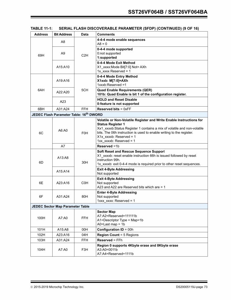
SST26VF064B / SST26VF064BA
69H
A8
C2H
4-4-4 mode enable sequencesA8 = 0
A90-4-4 mode supported0:not supported1:supported
A15:A100-4-4 Mode Exit MethodX1_xxxx:Mode Bit[7:0] Not= AXh1x_xxxx Reserved = 1
6AH
A19:A16
5CH
0-4-4 Mode Entry MethodX1xxb: M[7:0]=AXh1xxxb:Reserved =1
A22:A20 Quad Enable Requirements (QER)101b: Quad Enable is bit 1 of the configuration register.
A23 HOLD and Reset Disable0:feature is not supported
6BH A31:A24 FFH Reserved bits = 0xFFJEDEC Flash Parameter Table: 16th DWORD
6CA6:A0
F0H
Volatile or Non-Volatile Register and Write Enable Instructions for Status Register 1Xx1_xxxxb:Status Register 1 contains a mix of volatile and non-volatile bits. The 06h instruction is used to enable writing to the register.X1x_xxxxb: Reserved = 11xx_xxxxb: Reserved = 1
A7 Reserved =1b
6DA13:A8
30H
Soft Reset and Rescue Sequence SupportX1_xxxxb: reset enable instruction 66h is issued followed by reset instruction 99h.1x_xxxxb: exit 0-4-4 mode is required prior to other reset sequences.
A15:A14 Exit 4-Byte AddressingNot supported
6E A23:A16 C0HExit 4-Byte AddressingNot supportedA23 and A22 are Reserved bits which are = 1
6F A31:A24 80HEnter 4-Byte AddressingNot supported1xxx_xxxx: Reserved = 1
JEDEC Sector Map Parameter Table
100H A7:A0 FFH
Sector MapA7:A2=Reserved=111111bA1=Descriptor Type = Map=1bA0=Last map = 1b
101H A15:A8 00H Configuration ID = 00h102H A23:A16 04H Region Count = 5 Regions103H A31:A24 FFH Reserved = FFh
104H A7:A0 F3HRegion 0 supports 4Kbyte erase and 8Kbyte eraseA3:A0=0011bA7:A4=Reserved=1111b
TABLE 11-1: SERIAL FLASH DISCOVERABLE PARAMETER (SFDP) (CONTINUED) (9 OF 16)Address Bit Address Data Comments
2015-2019 Microchip Technology Inc. DS20005119J-page 73
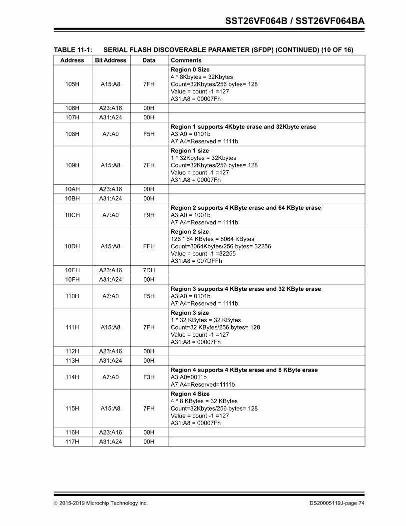
SST26VF064B / SST26VF064BA
105H A15:A8 7FH
Region 0 Size4 * 8Kbytes = 32KbytesCount=32Kbytes/256 bytes= 128Value = count -1 =127A31:A8 = 00007Fh
106H A23:A16 00H107H A31:A24 00H
108H A7:A0 F5HRegion 1 supports 4Kbyte erase and 32Kbyte eraseA3:A0 = 0101bA7:A4=Reserved = 1111b
109H A15:A8 7FH
Region 1 size1 * 32Kbytes = 32KbytesCount=32Kbytes/256 bytes= 128Value = count -1 =127A31:A8 = 00007Fh
10AH A23:A16 00H10BH A31:A24 00H
10CH A7:A0 F9HRegion 2 supports 4 KByte erase and 64 KByte eraseA3:A0 = 1001bA7:A4=Reserved = 1111b
10DH A15:A8 FFH
Region 2 size126 * 64 KBytes = 8064 KBytesCount=8064Kbytes/256 bytes= 32256Value = count -1 =32255A31:A8 = 007DFFh
10EH A23:A16 7DH10FH A31:A24 00H
110H A7:A0 F5HRegion 3 supports 4 KByte erase and 32 KByte eraseA3:A0 = 0101bA7:A4=Reserved = 1111b
111H A15:A8 7FH
Region 3 size1 * 32 KBytes = 32 KBytesCount=32 KBytes/256 bytes= 128Value = count -1 =127A31:A8 = 00007Fh
112H A23:A16 00H113H A31:A24 00H
114H A7:A0 F3HRegion 4 supports 4 KByte erase and 8 KByte eraseA3:A0=0011bA7:A4=Reserved=1111b
115H A15:A8 7FH
Region 4 Size4 * 8 KBytes = 32 KBytesCount=32Kbytes/256 bytes= 128Value = count -1 =127A31:A8 = 00007Fh
116H A23:A16 00H117H A31:A24 00H
TABLE 11-1: SERIAL FLASH DISCOVERABLE PARAMETER (SFDP) (CONTINUED) (10 OF 16)Address Bit Address Data Comments
2015-2019 Microchip Technology Inc. DS20005119J-page 74
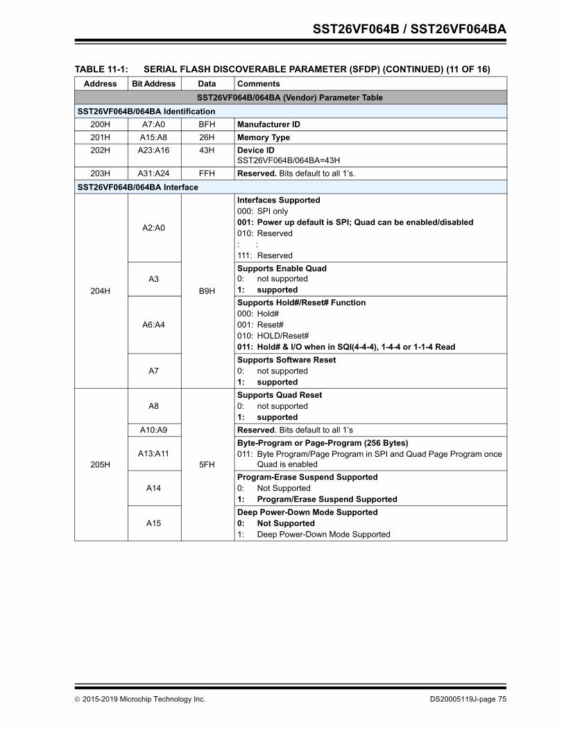
SST26VF064B / SST26VF064BA
SST26VF064B/064BA (Vendor) Parameter TableSST26VF064B/064BA Identification
200H A7:A0 BFH Manufacturer ID201H A15:A8 26H Memory Type202H A23:A16 43H Device ID
SST26VF064B/064BA=43H203H A31:A24 FFH Reserved. Bits default to all 1’s.
SST26VF064B/064BA Interface
204H
A2:A0
B9H
Interfaces Supported000: SPI only001: Power up default is SPI; Quad can be enabled/disabled010: Reserved: :111: Reserved
A3Supports Enable Quad0: not supported1: supported
A6:A4
Supports Hold#/Reset# Function000: Hold# 001: Reset#010: HOLD/Reset#011: Hold# & I/O when in SQI(4-4-4), 1-4-4 or 1-1-4 Read
A7Supports Software Reset0: not supported1: supported
205H
A8
5FH
Supports Quad Reset0: not supported1: supported
A10:A9 Reserved. Bits default to all 1’s
A13:A11Byte-Program or Page-Program (256 Bytes)011: Byte Program/Page Program in SPI and Quad Page Program once
Quad is enabled
A14Program-Erase Suspend Supported0: Not Supported1: Program/Erase Suspend Supported
A15Deep Power-Down Mode Supported0: Not Supported1: Deep Power-Down Mode Supported
TABLE 11-1: SERIAL FLASH DISCOVERABLE PARAMETER (SFDP) (CONTINUED) (11 OF 16)Address Bit Address Data Comments
2015-2019 Microchip Technology Inc. DS20005119J-page 75
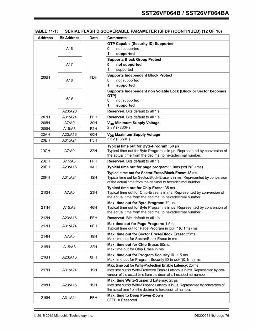
SST26VF064B / SST26VF064BA
206H
A16
FDH
OTP Capable (Security ID) Supported0: not supported1: supported
A17Supports Block Group Protect0: not supported1: supported
A18Supports Independent Block Protect0: not supported1: supported
A19
Supports Independent non Volatile Lock (Block or Sector becomes OTP)0: not supported1: supported
A23:A20 Reserved. Bits default to all 1’s.207H A31:A24 FFH Reserved. Bits default to all 1’s.208H A7:A0 30H VDD Minimum Supply Voltage
2.3V (F230H)209H A15:A8 F2H20AH A23:A16 60H VDD Maximum Supply Voltage
3.6V (F360H)20BH A31:A24 F3H
20CH A7:A0 32HTypical time out for Byte-Program: 50 µsTypical time out for Byte Program is in µs. Represented by conversion of the actual time from the decimal to hexadecimal number.
20DH A15:A8 FFH Reserved. Bits default to all 1’s.20EH A23:A16 0AH Typical time out for page program: 1.0ms (xxH*(0.1ms)
20FH A31:A24 12HTypical time out for Sector-Erase/Block-Erase: 18 msTypical time out for Sector/Block-Erase is in ms. Represented by conversion of the actual time from the decimal to hexadecimal number.
210H A7:A0 23HTypical time out for Chip-Erase: 35 msTypical time out for Chip-Erase is in ms. Represented by conversion of the actual time from the decimal to hexadecimal number.
211H A15:A8 46HMax. time out for Byte-Program: 70 µsTypical time out for Byte Program is in µs. Represented by conversion of the actual time from the decimal to hexadecimal number.
212H A23:A16 FFH Reserved. Bits default to all 1’s.
213H A31:A24 0FH Max time out for Page-Program: 1.5ms. Typical time out for Page Program in xxH * (0.1ms) ms
214H A7:A0 19H Max. time out for Sector Erase/Block Erase: 25ms.Max time out for Sector/Block Erase in ms
215H A15:A8 32H Max. time out for Chip Erase: 50ms.Max time out for Chip Erase in ms.
216H A23:A16 0FH Max. time out for Program Security ID: 1.5 msMax time out for Program Security ID in xxH*(0.1ms) ms
217H A31:A24 19HMax. time out for Write-Protection Enable Latency: 25 msMax time out for Write-Protection Enable Latency is in ms. Represented by con-version of the actual time from the decimal to hexadecimal number.
218H A23:A16 19HMax. time Write-Suspend Latency: 25 µsMax time out for Write-Suspend Latency is in µs. Represented by conversion of the actual time from the decimal to hexadecimal number.
219H A31:A24 FFH Max. time to Deep Power-Down0FFH = Reserved
TABLE 11-1: SERIAL FLASH DISCOVERABLE PARAMETER (SFDP) (CONTINUED) (12 OF 16)Address Bit Address Data Comments
2015-2019 Microchip Technology Inc. DS20005119J-page 76
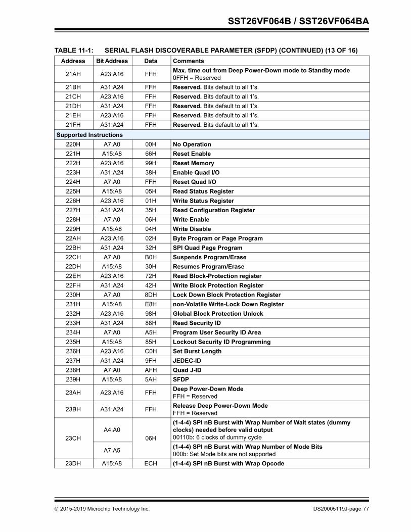
SST26VF064B / SST26VF064BA
21AH A23:A16 FFH Max. time out from Deep Power-Down mode to Standby mode0FFH = Reserved
21BH A31:A24 FFH Reserved. Bits default to all 1’s.21CH A23:A16 FFH Reserved. Bits default to all 1’s.21DH A31:A24 FFH Reserved. Bits default to all 1’s.21EH A23:A16 FFH Reserved. Bits default to all 1’s.21FH A31:A24 FFH Reserved. Bits default to all 1’s.
Supported Instructions220H A7:A0 00H No Operation221H A15:A8 66H Reset Enable222H A23:A16 99H Reset Memory223H A31:A24 38H Enable Quad I/O224H A7:A0 FFH Reset Quad I/O225H A15:A8 05H Read Status Register226H A23:A16 01H Write Status Register227H A31:A24 35H Read Configuration Register228H A7:A0 06H Write Enable229H A15:A8 04H Write Disable22AH A23:A16 02H Byte Program or Page Program22BH A31:A24 32H SPI Quad Page Program22CH A7:A0 B0H Suspends Program/Erase22DH A15:A8 30H Resumes Program/Erase22EH A23:A16 72H Read Block-Protection register22FH A31:A24 42H Write Block Protection Register230H A7:A0 8DH Lock Down Block Protection Register231H A15:A8 E8H non-Volatile Write-Lock Down Register232H A23:A16 98H Global Block Protection Unlock233H A31:A24 88H Read Security ID234H A7:A0 A5H Program User Security ID Area235H A15:A8 85H Lockout Security ID Programming236H A23:A16 C0H Set Burst Length237H A31:A24 9FH JEDEC-ID238H A7:A0 AFH Quad J-ID239H A15:A8 5AH SFDP
23AH A23:A16 FFH Deep Power-Down ModeFFH = Reserved
23BH A31:A24 FFH Release Deep Power-Down ModeFFH = Reserved
23CHA4:A0
06H
(1-4-4) SPI nB Burst with Wrap Number of Wait states (dummy clocks) needed before valid output00110b: 6 clocks of dummy cycle
A7:A5 (1-4-4) SPI nB Burst with Wrap Number of Mode Bits000b: Set Mode bits are not supported
23DH A15:A8 ECH (1-4-4) SPI nB Burst with Wrap Opcode
TABLE 11-1: SERIAL FLASH DISCOVERABLE PARAMETER (SFDP) (CONTINUED) (13 OF 16)Address Bit Address Data Comments
2015-2019 Microchip Technology Inc. DS20005119J-page 77
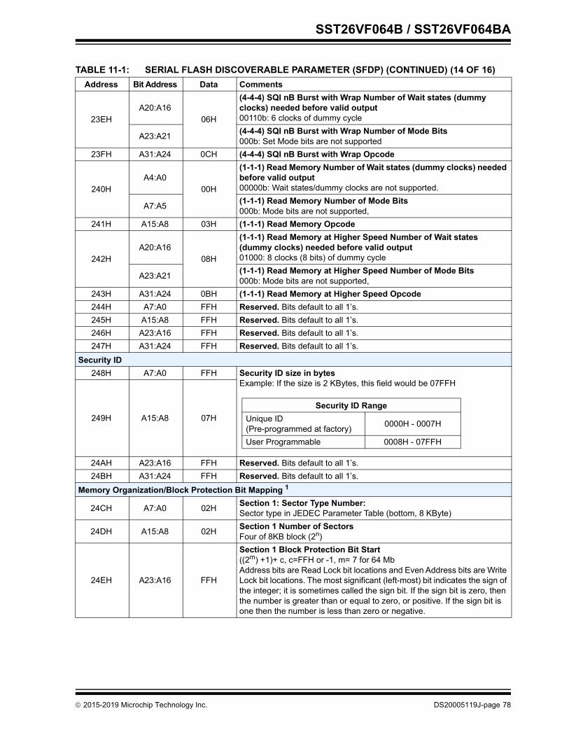
SST26VF064B / SST26VF064BA
23EHA20:A16
06H
(4-4-4) SQI nB Burst with Wrap Number of Wait states (dummy clocks) needed before valid output00110b: 6 clocks of dummy cycle
A23:A21 (4-4-4) SQI nB Burst with Wrap Number of Mode Bits000b: Set Mode bits are not supported
23FH A31:A24 0CH (4-4-4) SQI nB Burst with Wrap Opcode
240HA4:A0
00H
(1-1-1) Read Memory Number of Wait states (dummy clocks) needed before valid output00000b: Wait states/dummy clocks are not supported.
A7:A5 (1-1-1) Read Memory Number of Mode Bits000b: Mode bits are not supported,
241H A15:A8 03H (1-1-1) Read Memory Opcode
242HA20:A16
08H
(1-1-1) Read Memory at Higher Speed Number of Wait states (dummy clocks) needed before valid output01000: 8 clocks (8 bits) of dummy cycle
A23:A21 (1-1-1) Read Memory at Higher Speed Number of Mode Bits000b: Mode bits are not supported,
243H A31:A24 0BH (1-1-1) Read Memory at Higher Speed Opcode244H A7:A0 FFH Reserved. Bits default to all 1’s.245H A15:A8 FFH Reserved. Bits default to all 1’s.246H A23:A16 FFH Reserved. Bits default to all 1’s.247H A31:A24 FFH Reserved. Bits default to all 1’s.
Security ID248H A7:A0 FFH Security ID size in bytes
Example: If the size is 2 KBytes, this field would be 07FFH
249H A15:A8 07H
24AH A23:A16 FFH Reserved. Bits default to all 1’s.24BH A31:A24 FFH Reserved. Bits default to all 1’s.
Memory Organization/Block Protection Bit Mapping 1
24CH A7:A0 02H Section 1: Sector Type Number:Sector type in JEDEC Parameter Table (bottom, 8 KByte)
24DH A15:A8 02H Section 1 Number of SectorsFour of 8KB block (2n)
24EH A23:A16 FFH
Section 1 Block Protection Bit Start((2m) +1)+ c, c=FFH or -1, m= 7 for 64 MbAddress bits are Read Lock bit locations and Even Address bits are Write Lock bit locations. The most significant (left-most) bit indicates the sign of the integer; it is sometimes called the sign bit. If the sign bit is zero, then the number is greater than or equal to zero, or positive. If the sign bit is one then the number is less than zero or negative.
TABLE 11-1: SERIAL FLASH DISCOVERABLE PARAMETER (SFDP) (CONTINUED) (14 OF 16)Address Bit Address Data Comments
Security ID RangeUnique ID (Pre-programmed at factory) 0000H - 0007H
User Programmable 0008H - 07FFH
2015-2019 Microchip Technology Inc. DS20005119J-page 78
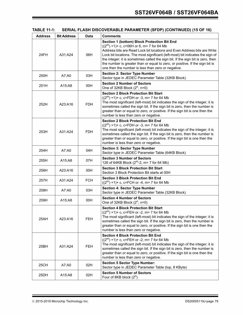
SST26VF064B / SST26VF064BA
24FH A31:A24 06H
Section 1 (bottom) Block Protection Bit End((2m) +1)+ c, c=06H or 6, m= 7 for 64 MbAddress bits are Read Lock bit locations and Even Address bits are Write Lock bit locations. The most significant (left-most) bit indicates the sign of the integer; it is sometimes called the sign bit. If the sign bit is zero, then the number is greater than or equal to zero, or positive. If the sign bit is one then the number is less than zero or negative.
250H A7:A0 03H Section 2: Sector Type NumberSector type in JEDEC Parameter Table (32KB Block)
251H A15:A8 00H Section 2 Number of SectorsOne of 32KB Block (2n, n=0)
252H A23:A16 FDH
Section 2 Block Protection Bit Start((2m) +1)+ c, c=FDH or -3, m= 7 for 64 MbThe most significant (left-most) bit indicates the sign of the integer; it is sometimes called the sign bit. If the sign bit is zero, then the number is greater than or equal to zero, or positive. If the sign bit is one then the number is less than zero or negative.
253H A31:A24 FDH
Section 2 Block Protection Bit End((2m) +1)+ c, c=FDH or -3, m= 7 for 64 MbThe most significant (left-most) bit indicates the sign of the integer; it is sometimes called the sign bit. If the sign bit is zero, then the number is greater than or equal to zero, or positive. If the sign bit is one then the number is less than zero or negative.
254H A7:A0 04H Section 3: Sector Type NumberSector type in JEDEC Parameter Table (64KB Block)
255H A15:A8 07H Section 3 Number of Sectors126 of 64KB Block (2m-2, m= 7 for 64 Mb)
256H A23:A16 00H Section 3 Block Protection Bit StartSection 3 Block Protection Bit starts at 00H
257H A31:A24 FCH Section 3 Block Protection Bit End((2m) +1)+ c, c=FCH or -4, m= 7 for 64 Mb
258H A7:A0 03H Section 4: Sector Type NumberSector type in JEDEC Parameter Table (32KB Block)
259H A15:A8 00H Section 4 Number of SectorsOne of 32KB Block (2n, n=0)
25AH A23:A16 FEH
Section 4 Block Protection Bit Start((2m) +1)+ c, c=FEH or -2, m= 7 for 64 MbThe most significant (left-most) bit indicates the sign of the integer; it is sometimes called the sign bit. If the sign bit is zero, then the number is greater than or equal to zero, or positive. If the sign bit is one then the number is less than zero or negative.
25BH A31:A24 FEH
Section 4 Block Protection Bit End((2m) +1)+ c, c=FEH or -2, m= 7 for 64 MbThe most significant (left-most) bit indicates the sign of the integer; it is sometimes called the sign bit. If the sign bit is zero, then the number is greater than or equal to zero, or positive. If the sign bit is one then the number is less than zero or negative.
25CH A7:A0 02H Section 5 Sector Type Number:Sector type in JEDEC Parameter Table (top, 8 KByte)
25DH A15:A8 02H Section 5 Number of SectorsFour of 8KB block (2n)
TABLE 11-1: SERIAL FLASH DISCOVERABLE PARAMETER (SFDP) (CONTINUED) (15 OF 16)Address Bit Address Data Comments
2015-2019 Microchip Technology Inc. DS20005119J-page 79
SST26VF064B / SST26VF064BA
11.1 Mapping Guidance DetailsThe SFDP Memory Organization/Block Protection BitMapping defines the memory organization includinguniform sector/block sizes and different contiguoussectors/blocks sizes. In addition, this bit defines the
number of these uniform and different sectors/blocksfrom address 000000H to the full range of Memory andthe associated Block Locking Register bits of each sec-tor/block.Each major Section is defined as follows:
A Major Section consists of Sector Type Number, Num-ber of Sector of this type, and the Block-Protection BitStart/End locations. This is tied directly to JEDEC FlashParameter Table Sector Size Type (in 7th DWORD and8th DWORD section). Note that the contiguous 4KByteSectors across the full memory range are not includedon this section because they are not defined in theJEDEC Flash Parameter Table Sector Size Type sec-tion. Only the sectors/blocks that are dependently tiedwith the Block-Protection Register bits are defined. Amajor section is a partition of contiguous same-sizesectors/blocks. There will be several Major Sections asyou dissect across memory from 000000h to the fullrange. Similar sector/block size that re-appear may bedefined as a different Major Section.
11.1.1 SECTOR TYPE NUMBERSector Type Number is the sector/block size typeddefined in JEDEC Flash Parameter Table: SFDPaddress locations 4CH, 4EH, 50H, and 52H. For SFDPaddress location 4CH, which is Sector Type 1, the sizeis represented by 01H; SFDP address location 4EH,Sector Type 2, size is represented by 02H; SFDPaddress location 50H, Sector Type 3, size is repre-sented by 03H; and SFDP address location 52H, Sec-
tor Type 4, size is represented by 04H. ContiguousSame Sector Type # Size can re-emerge across thememory range and this Sector Type # will indicate thatit is a separate/independent Major Section from theprevious contiguous sectors/blocks.
11.1.2 NUMBER OF SECTORSNumber of Sectors represents the number of contigu-ous sectors/blocks with similar size. A formula calcu-lates the contiguous sectors/blocks with similar size.Given the sector/block size, type, and the number ofsectors, the address range of these sectors/blocks canbe determined along with specific Block Locking Reg-ister bits that control the read/write protection of eachsectors/blocks.
25EH A23:A16 07H
Section 5 Block Protection Bit Start((2m) +1)+ c, c=07H or 7, m= 7 for 64 MbAddress bits are Read Lock bit locations and Even Address bits are Write Lock bit locations. The most significant (left-most) bit indicates the sign of the integer; it is sometimes called the sign bit. If the sign bit is zero, then the number is greater than or equal to zero, or positive. If the sign bit is one then the number is less than zero or negative.
25FH A31:A24 0EH
Section 5 (Top) Block Protection Bit End(((2m) +1)+ c, c=0EH or 14, m= 7 for 64 Mb,Address bits are Read Lock bit locations and Even Address bits are Write Lock bit locations. The most significant (left-most) bit indicates the sign of the integer; it is sometimes called the sign bit. If the sign bit is zero, then the number is greater than or equal to zero, or positive. If the sign bit is one then the number is less than zero or negative.
1. See “Mapping Guidance Details” for more detailed mapping information
TABLE 11-1: SERIAL FLASH DISCOVERABLE PARAMETER (SFDP) (CONTINUED) (16 OF 16)Address Bit Address Data Comments
TABLE 11-2: SECTION DEFINITIONMajor Section X Section X: Sector Type Number
Section X: Number of SectorsSection X: Block-Protection Register Bit Start LocationSection X: Block-Protection Register Bit End Location
2015-2019 Microchip Technology Inc. DS20005119J-page 80
SST26VF064B / SST26VF064BA
11.1.3 BLOCK-PROTECTION REGISTER BIT START LOCATION (BPSL)
Block-Protection Register Bit Start Location (BPSL)designates the start bit location in the Block-ProtectionRegister where the first sector/block of this Major Sec-tion begins. If the value of BPSL is 00H, this location isthe 0 bit location. If the value is other than 0, then thisvalue is a constant value adder (c) for a given formula,(2m + 1) + (c). See “Memory Configuration”.From the initial location, there will be a bit location forevery increment by 1 until it reaches the Block Protec-tion Register Bit End Location (BPEL). This numberrange from BPSL to BPEL will correspond to, and beequal to, the number of sectors/blocks on this MajorSection.
11.1.4 BLOCK PROTECTION REGISTER BIT END LOCATION (BPEL)
Block Protection Register Bit End Location designatesthe end bit location in the Block Protection Register bitwhere the last sector/block of this Major Section ends.The value in this field is a constant value adder (c) fora given formula or equation, (2m + 1) + (c). See “Mem-ory Configuration”
11.1.5 MEMORY CONFIGURATIONFor the SST26VF064B/064BA family, the memory con-figuration is setup with different contiguous block sizesfrom bottom to the top of the memory. For example,starting from bottom of memory it has four 8KByteblocks, one 32KByte block, x number of 64KByteblocks depending on memory size, then one 32KByteblock, and four 8KByte block on the top of memory. SeeTable 11-3.
Classifying these sector/block sizes via the SectorType derived from JEDEC Flash Parameter Table:SFDP address locations 4EH, 50H, and 52H is as fol-lows:• 8KByte Blocks are classified as Sector Type 2
(@4EH of SFDP)• 32KByte Blocks are classified as Sector Type 3
(@50H of SFDP)• 64KByte Blocks are classified as Sector Type 4
(@52H of SFDP)
For the Number of Sectors associated with the contig-uous sectors/blocks, a formula is used to determine thenumber of sectors/blocks of these Sector Types:• 8KByte Block (Type 2) is calculated by 2n. n is a byte.• 32KByte Block (Type 3) is calculated by 2n. n is a
byte.• 64KByte Block (Type 4) is calculated by (2m - 2). m
can either be a 4, 5, 6, 7 or 8 depending on the mem-ory size. This m field is going to be used for the 64KByte Block Section and will also be used for the Block Protection Register Bit Location formula.
TABLE 11-3: MEMORY BLOCK DIAGRAM REPRESENTATION8 KByte Bottom Block (from 000000H)
Section 1: Sector Type NumberSection 1: Number of SectorsSection 1: Block-Protection Register Bit Start LocationSection 1: Block-Protection Register Bit End Location
32 KByte Section 2: Sector Type NumberSection 2: Number of SectorsSection 2: Block-Protection Register Bit Start LocationSection 2: Block-Protection Register Bit End Location
64 KByte Section 3: Sector Type NumberSection 3: Number of SectorsSection 3: Block-Protection Register Bit Start LocationSection 3: Block-Protection Register Bit End Location
32 KByte Section 4: Sector Type NumberSection 4: Number of SectorsSection 4: Block-Protection Register Bit Start LocationSection 4: Block-Protection Register Bit End Location
8 KByte (Top Block) Section 5: Sector Type NumberSection 5: Number of SectorsSection 5: Block-Protection Register Bit Start LocationSection 5: Block-Protection Register Bit End Location
2015-2019 Microchip Technology Inc. DS20005119J-page 81
SST26VF064B / SST26VF064BA
m will have a constant value for specific densities andis defined as:• 8Mbit = 4• 16Mbit = 5• 32Mbit = 6 • 64Mbit = 7 • 128Mbit = 8Block Protect Register Start/End Bits are mapped in theSFDP by using the formula (2m + 1) + (c). “m” is a con-stant value that represents the different densities from8Mbit to 128Mbit (used also in the formula calculatingnumber of 64Kbyte Blocks above). The values that are
going to be placed in the Block Protection Bit Start/Endfield table are the constant value adder (c) in the for-mula and are represented in two’s compliment exceptwhen the value is 00H. If the value is 00H, this locationis the 0 bit location. If the value is other than 0, then thisis a constant value adder (c) that will be used in the for-mula. The most significant (left most) bit indicates thesign of the integer; it is sometimes called the sign bit.If the sign bit is zero, then the number is greater than orequal to zero, or positive. If the sign bit is one, then thenumber is less than zero, or negative.See Table 11-4 for an example of this formula.
TABLE 11-4: BPSL/BPEL EQUATION WITH ACTUAL CONSTANT ADDER DERIVED FROM THE FORMULA (2M + 1) + (C)
Block Size 8 Mbit to 128 Mbit Comments8 KByte (Type 2) Bottom BPSL = (2m + 1) + 0FFH
BPEL = (2m + 1) + 04H0FFH = -1; 06H = 6Odd address bits are Read-Lock bit locations and even address bits are Write-Lock bit locations.
32 KByte (Type 3) BPSL = BPEL= (2m + 1) + 0FDH 0FDH= -364 KByte (Type 4) BPSL = 00H
BPEL = (2m + 1) + 0FCH00H is Block-Protection Register bit 0 location; 0FCH = -4
32 KByte (Type 3) BPSL = BPEL= (2m + 1) + 0FEH 0FEH=-28 KByte (Type 2) Top BPSL = (2m + 1) + 07H
BPEL = (2m + 1) + 0EH07H = 7; 0EH = 14Odd address bits are Read-Lock bit locations and even address bits are Write-Lock bit locations.
2015-2019 Microchip Technology Inc. DS20005119J-page 82
2019 Microchip Technology Inc. DS20005119J-page 83
SST26VF064B / SST26VF064BA
THE MICROCHIP WEBSITEMicrochip provides online support via our WWW site atwww.microchip.com. This website is used as a meansto make files and information easily available tocustomers. Accessible by using your favorite Internetbrowser, the website contains the following information:• Product Support – Data sheets and errata,
application notes and sample programs, design resources, user’s guides and hardware support documents, latest software releases and archived software
• General Technical Support – Frequently Asked Questions (FAQ), technical support requests, online discussion groups, Microchip consultant program member listing
• Business of Microchip – Product selector and ordering guides, latest Microchip press releases, listing of seminars and events, listings of Microchip sales offices, distributors and factory representatives
CUSTOMER CHANGE NOTIFICATION SERVICEMicrochip’s customer notification service helps keepcustomers current on Microchip products. Subscriberswill receive e-mail notification whenever there arechanges, updates, revisions or errata related to aspecified product family or development tool of interest.To register, access the Microchip website atwww.microchip.com. Under “Support”, click on“Customer Change Notification” and follow theregistration instructions.
CUSTOMER SUPPORTUsers of Microchip products can receive assistancethrough several channels:• Distributor or Representative• Local Sales Office• Field Application Engineer (FAE)• Technical SupportCustomers should contact their distributor,representative or Field Application Engineer (FAE) forsupport. Local sales offices are also available to helpcustomers. A listing of sales offices and locations isincluded in the back of this document.Technical support is available through the websiteat: http://microchip.com/support
Note the following details of the code protection feature on Microchip devices:• Microchip products meet the specification contained in their particular Microchip Data Sheet.
• Microchip believes that its family of products is one of the most secure families of its kind on the market today, when used in the intended manner and under normal conditions.
• There are dishonest and possibly illegal methods used to breach the code protection feature. All of these methods, to our knowledge, require using the Microchip products in a manner outside the operating specifications contained in Microchip’s Data Sheets. Most likely, the person doing so is engaged in theft of intellectual property.
• Microchip is willing to work with the customer who is concerned about the integrity of their code.
• Neither Microchip nor any other semiconductor manufacturer can guarantee the security of their code. Code protection does not mean that we are guaranteeing the product as “unbreakable.”
Code protection is constantly evolving. We at Microchip are committed to continuously improving the code protection features of ourproducts. Attempts to break Microchip’s code protection feature may be a violation of the Digital Millennium Copyright Act. If such actsallow unauthorized access to your software or other copyrighted work, you may have a right to sue for relief under that Act.
Information contained in this publication regarding deviceapplications and the like is provided only for your convenienceand may be superseded by updates. It is your responsibility toensure that your application meets with your specifications.MICROCHIP MAKES NO REPRESENTATIONS ORWARRANTIES OF ANY KIND WHETHER EXPRESS ORIMPLIED, WRITTEN OR ORAL, STATUTORY OROTHERWISE, RELATED TO THE INFORMATION,INCLUDING BUT NOT LIMITED TO ITS CONDITION,QUALITY, PERFORMANCE, MERCHANTABILITY ORFITNESS FOR PURPOSE. Microchip disclaims all liabilityarising from this information and its use. Use of Microchipdevices in life support and/or safety applications is entirely atthe buyer’s risk, and the buyer agrees to defend, indemnify andhold harmless Microchip from any and all damages, claims,suits, or expenses resulting from such use. No licenses areconveyed, implicitly or otherwise, under any Microchipintellectual property rights unless otherwise stated.
2019 Microchip Technology Inc.
Microchip received ISO/TS-16949:2009 certification for its worldwide headquarters, design and wafer fabrication facilities in Chandler and Tempe, Arizona; Gresham, Oregon and design centers in California and India. The Company’s quality system processes and procedures are for its PIC® MCUs and dsPIC® DSCs, KEELOQ® code hopping devices, Serial EEPROMs, microperipherals, nonvolatile memory and analog products. In addition, Microchip’s quality system for the design and manufacture of development systems is ISO 9001:2000 certified.
QUALITY MANAGEMENT SYSTEM CERTIFIED BY DNV
== ISO/TS 16949 ==
TrademarksThe Microchip name and logo, the Microchip logo, AnyRate, AVR, AVR logo, AVR Freaks, BitCloud, chipKIT, chipKIT logo, CryptoMemory, CryptoRF, dsPIC, FlashFlex, flexPWR, Heldo, JukeBlox, KeeLoq, Kleer, LANCheck, LINK MD, maXStylus, maXTouch, MediaLB, megaAVR, MOST, MOST logo, MPLAB, OptoLyzer, PIC, picoPower, PICSTART, PIC32 logo, Prochip Designer, QTouch, SAM-BA, SpyNIC, SST, SST Logo, SuperFlash, tinyAVR, UNI/O, and XMEGA are registered trademarks of Microchip Technology Incorporated in the U.S.A. and other countries.ClockWorks, The Embedded Control Solutions Company, EtherSynch, Hyper Speed Control, HyperLight Load, IntelliMOS, mTouch, Precision Edge, and Quiet-Wire are registered trademarks of Microchip Technology Incorporated in the U.S.A.Adjacent Key Suppression, AKS, Analog-for-the-Digital Age, Any Capacitor, AnyIn, AnyOut, BodyCom, CodeGuard, CryptoAuthentication, CryptoAutomotive, CryptoCompanion, CryptoController, dsPICDEM, dsPICDEM.net, Dynamic Average Matching, DAM, ECAN, EtherGREEN, In-Circuit Serial Programming, ICSP, INICnet, Inter-Chip Connectivity, JitterBlocker, KleerNet, KleerNet logo, memBrain, Mindi, MiWi, motorBench, MPASM, MPF, MPLAB Certified logo, MPLIB, MPLINK, MultiTRAK, NetDetach, Omniscient Code Generation, PICDEM, PICDEM.net, PICkit, PICtail, PowerSmart, PureSilicon, QMatrix, REAL ICE, Ripple Blocker, SAM-ICE, Serial Quad I/O, SMART-I.S., SQI, SuperSwitcher, SuperSwitcher II, Total Endurance, TSHARC, USBCheck, VariSense, ViewSpan, WiperLock, Wireless DNA, and ZENA are trademarks of Microchip Technology Incorporated in the U.S.A. and other countries.SQTP is a service mark of Microchip Technology Incorporated in the U.S.A.Silicon Storage Technology is a registered trademark of Microchip Technology Inc. in other countries.GestIC is a registered trademark of Microchip Technology Germany II GmbH & Co. KG, a subsidiary of Microchip Technology Inc., in other countries. All other trademarks mentioned herein are property of their respective companies.© 2018, Microchip Technology Incorporated, All Rights Reserved.ISBN: 978-1-5224-4544-9
DS20005119J-page 84

DS20005119J-page 85 2019 Microchip Technology Inc.
AMERICASCorporate Office2355 West Chandler Blvd.Chandler, AZ 85224-6199Tel: 480-792-7200 Fax: 480-792-7277Technical Support: http://www.microchip.com/supportWeb Address: www.microchip.comAtlantaDuluth, GA Tel: 678-957-9614 Fax: 678-957-1455Austin, TXTel: 512-257-3370 BostonWestborough, MA Tel: 774-760-0087 Fax: 774-760-0088ChicagoItasca, IL Tel: 630-285-0071 Fax: 630-285-0075DallasAddison, TX Tel: 972-818-7423 Fax: 972-818-2924DetroitNovi, MI Tel: 248-848-4000Houston, TX Tel: 281-894-5983IndianapolisNoblesville, IN Tel: 317-773-8323Fax: 317-773-5453Tel: 317-536-2380Los AngelesMission Viejo, CA Tel: 949-462-9523Fax: 949-462-9608Tel: 951-273-7800 Raleigh, NC Tel: 919-844-7510New York, NY Tel: 631-435-6000San Jose, CA Tel: 408-735-9110Tel: 408-436-4270Canada - TorontoTel: 905-695-1980 Fax: 905-695-2078
ASIA/PACIFICAustralia - SydneyTel: 61-2-9868-6733China - BeijingTel: 86-10-8569-7000 China - ChengduTel: 86-28-8665-5511China - ChongqingTel: 86-23-8980-9588China - DongguanTel: 86-769-8702-9880 China - GuangzhouTel: 86-20-8755-8029 China - HangzhouTel: 86-571-8792-8115 China - Hong Kong SARTel: 852-2943-5100 China - NanjingTel: 86-25-8473-2460China - QingdaoTel: 86-532-8502-7355China - ShanghaiTel: 86-21-3326-8000 China - ShenyangTel: 86-24-2334-2829China - ShenzhenTel: 86-755-8864-2200 China - SuzhouTel: 86-186-6233-1526 China - WuhanTel: 86-27-5980-5300China - XianTel: 86-29-8833-7252China - XiamenTel: 86-592-2388138 China - ZhuhaiTel: 86-756-3210040
ASIA/PACIFICIndia - BangaloreTel: 91-80-3090-4444 India - New DelhiTel: 91-11-4160-8631India - PuneTel: 91-20-4121-0141Japan - OsakaTel: 81-6-6152-7160 Japan - TokyoTel: 81-3-6880- 3770 Korea - DaeguTel: 82-53-744-4301Korea - SeoulTel: 82-2-554-7200Malaysia - Kuala LumpurTel: 60-3-7651-7906Malaysia - PenangTel: 60-4-227-8870Philippines - ManilaTel: 63-2-634-9065SingaporeTel: 65-6334-8870Taiwan - Hsin ChuTel: 886-3-577-8366Taiwan - KaohsiungTel: 886-7-213-7830Taiwan - TaipeiTel: 886-2-2508-8600 Thailand - BangkokTel: 66-2-694-1351Vietnam - Ho Chi MinhTel: 84-28-5448-2100
EUROPEAustria - WelsTel: 43-7242-2244-39Fax: 43-7242-2244-393Denmark - CopenhagenTel: 45-4450-2828 Fax: 45-4485-2829Finland - EspooTel: 358-9-4520-820France - ParisTel: 33-1-69-53-63-20 Fax: 33-1-69-30-90-79 Germany - GarchingTel: 49-8931-9700Germany - HaanTel: 49-2129-3766400Germany - HeilbronnTel: 49-7131-72400Germany - KarlsruheTel: 49-721-625370Germany - MunichTel: 49-89-627-144-0 Fax: 49-89-627-144-44Germany - RosenheimTel: 49-8031-354-560Israel - Ra’anana Tel: 972-9-744-7705Italy - Milan Tel: 39-0331-742611 Fax: 39-0331-466781Italy - PadovaTel: 39-049-7625286 Netherlands - DrunenTel: 31-416-690399 Fax: 31-416-690340Norway - TrondheimTel: 47-7288-4388Poland - WarsawTel: 48-22-3325737 Romania - BucharestTel: 40-21-407-87-50Spain - MadridTel: 34-91-708-08-90Fax: 34-91-708-08-91Sweden - GothenbergTel: 46-31-704-60-40Sweden - StockholmTel: 46-8-5090-4654UK - WokinghamTel: 44-118-921-5800Fax: 44-118-921-5820
Worldwide Sales and Service
05/14/19