Embed Size (px)
Citation preview
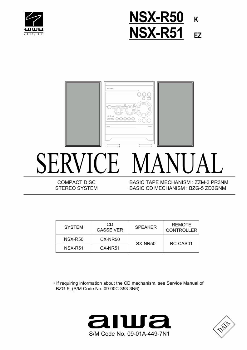
SERVICE MANUAL
DATA
COMPACT DISCSTEREO SYSTEM
BASIC TAPE MECHANISM : ZZM-3 PR3NMBASIC CD MECHANISM : BZG-5 ZD3GNM
NSX-R50NSX-R51
K
EZ
S/M Code No. 09-01A-449-7N1
• If requiring information about the CD mechanism, see Service Manual of BZG-5, (S/M Code No. 09-00C-353-3N6).
SPEAKERSYSTEM
CX-NR50RC-CAS01
CDCASSEIVER
REMOTECONTROLLER
SX-NR50NSX-R50
NSX-R51 CX-NR51
!"#$ %&'&"(&$
%&&"&$ %)*! ++&'(& +)*! ,
! " -.+/0+/
"!1231&*45+$- ./0/"!1231&*45+%'+$67.45894:;</6-.'/0'/
#$ 3"%/1&1!145=84<$
" )46<*=8>.!)%" 9;6=?6-9.!!
;<569.%'!!
&''(&)#*+ +&1'#,#" @&# $ =:$ 6:?.#A&>
6:?'.*#A&>1
B&(- 9!#"λ C!$(# #' . . "&1 $ #$ 3"&1 $
/ !, '%)=:1 !# " / !# " $ $ /6:<!./
/6:<! .(/( BB( 'B%'+B%!! 0 (&
'"* %A1 #B"!#$'"* / .!!
2.!!9.'!!!>'"$# !( BB( 'B%'+B'!! 0 +&
!
!"#$$%&'##&"%$%(())! *("% #&++& *&'##,-./$$++!!"%"#())! #!0!))! +!!#!! !)#"+#!! *&'# #&/&%#(10!))"+((+)(-*!% 2 ')"##&0&))$ %&*'&##,&))$)!+$1+&#$")'))$
!33!1!#$% !%0&%4+ 35 !%%!# +&## &% 0!4 +-+3$"6"$1!+ " 4$%%! 71(*+!%0"+"%8 *!% !%0&%4!1$%(#+&##!+ 6,1 -+'%)"%8 )!+$1+#15)%"%8 +- ,0$1+*1"4$181&%+$%6,1)!+$1*)!++2
+$-6-%#1-)+-1!4/(+#$%#+-13$16-1!%$-631-$ 4(1$+ -#.$1 #.!% #.-+$ +3$"6"$4 .$1"% !' 1$+()# "%.!9!14-(+1!4"!#"-%$:3-+(1$
;(#"))"+!#"-% 4$ -!%4$+ 1<8)!8$+ -( 31-<4(1$+!(#1$+=($$(:+3<"6"<+3$(#$%#1!>%$1(%$4!%8$1$(+$$:3-+"#"-%!(:1!4"!#"-%+
+'%)"8)!+$1+#5)"%80$457%"%8%51+"**$1.$4+!671'4$1$$1(4$!66(%*#"-%%485(4+?##$)+$6-1+#15)"%8
."+ -3!# "+ 3)!'$1 "+ )!++"6"$4 !+ ! 231-4(#.$2 )!7$)"+)-!#$4-%#.$1$!1$:#$1"-1
2 2 2 2
"
"
#$
%&'(&&)"
*
– 4 –
NOTE ON BEFORE STARTING REPAIR
Charging voltage (V) Discharging Rated power (W) Parts number
(C101, 102) resistor (Ω)
25-48 100 3 87-A00-247-090
49-140 220 5 87-A00-232-090
Note: The reference numbers (C101, C102) of the electrolytic capacitors can change depending on the models. Be sure to check thereference numbers of the charging capacitors on schematic diagram before starting the discharging work.
2. Check items before exchanging the MICROCOMPUTER
Be sure to check the following items before exchanging the MICROCOMPUTER. Exchange the MICROCOMPUTER after confirmingthat the MICROCOMPUTER is surely defective.
2-1. Regarding the HOLD terminal of the MICROCOMPUTER
When the HOLD terminal (INPUT) of the MICROCOMPUTER is “H”, the MICROCOMPUTER is judged to be operating correctly.When this terminal is “L”, the main power cannot be turned on. Therefore, be sure to check the terminal voltage of the HOLDterminal before exchange.When the MICROCOMPUTER is not defective, the HOLD terminal can also go “L” when the POWER AMPLIFIER has anyabnormalities that triggers the abnormality detection circuit on the MAIN C. B. that sets the HOLD terminal to “L”.
• Good or no good judgement of the MICROCOMPUTER
11111 Turn on the AC main power.22222 Confirm that the main power is turned on and the HOLD terminal of the MICROCOMPUTER keeps the “H” level or not.33333 When the HOLD terminal is “L” level, the abnormality detection circuit is judged to be working correctly and the
MICROCOMPUTER is judged to be good.
1. Forced discharge of electrolytic capacitor of power supply block
When repair is going to be attempted in the set that uses relay circuit in the power supply block, electric potential is kept charged acrossthe electrolytic capacitors (C101, 102) even though AC power cord is removed. If repair is attempted in this condition, secondary defectcan occur.In order to prevent the secondary trouble, perform the following measures before starting repair work.
Discharge procedure
11111 Remove the AC power cord.22222 Connect a discharging resistor at an end of lead wire that
has clips at both ends. Connect the other end of the leadwire to metal chassis.
33333 Contact the other end of the discharging resistor to thepositive (+) side (+VH) of C101. (For two seconds)
44444 Contact the same end of the discharging resistor as step33333 to the negative (-) side (-VH) of C102 in the same way.(For two seconds)
55555 Check that voltage across C101 and C102 has decreasedto 1 V or less using a multimeter or an oscilloscope.
Select a discharging resistor referring to the following table. Fig-1
MAIN C.B
D101
C101 C102
2 2
3 4
– 5 –
In such a case, check also if the POWER AMPLIFIER circuit or power supply circuit has any abnormalities or not.
2-2. Regarding resetThere are cases that the machine does not work correctly because the MICROCOMPUTER is not reset even though the AC powercord is re-inserted, or the software reset (pressing the STOP key + POWER key) is performed.When the above described phenomenon occurs, it can lead to wrong judgement as if the MICROCOMPUTER is defective and toexchange the MICROCOMPUTER. In such a case, perform the forced-reset by the following procedure and check good or nogood of the MICROCOMPUTER.11111 Remove the AC power cord.
22222 Short both ends of the electrolytic capacitor C113 that is connected to VDD of the MICROCOMPUTER with tweezers.33333 Connect the AC power cord again. If the MICROCOMPUTER returns to the normal operation, the MICROCOMPUTER is
good.
Note: The reference number or MICROCOMPUTER pin number of transistor (Q110) and electrolytic capacitor (C113) can change dependingon the models. Be sure to check the reference numbers on schematic diagram before starting the discharging work.
2-3. Confirmation of soldering state of MICROCOMPUTER
Check the soldering state of the MICROCOMPUTER in addition to the above described procedures. Be sure to exchange theMICROCOMPUTER after surely confirming that the trouble is not caused by poor soldering but the MICROCOMPUTER itself.
Fig-2-2
MICRO-COMPUTER
MIC
ROCOMPUTER
FRONT C.B
FRONT C.B
VSS
VDDC113
*
%
C113
1815
Short with tweezers.
!"!
! #! ! $#!! !
! ! $!! ! !! $!!$
! %#!&'! ! ! $
$! $!! (!
! ($! %"'! $! $!
! !
"
" !# " ! " %'!
" " " # %'! )! )
! )! )! *
)
) ) ) ) )
) ) ) # #
# # # # #
# # # ) #
# # ) )# #
# ) *$ *$ )#
)# # #
* * # # *
* ) ) ) )
)
+! +! ) ) )
) ) ) ) )
#
# * *
# )# )# * )
) # * )# )#
* * ) ) )
) # #
# )
* ) *
* )$
)$ )$ )$ )# )#
)# )# )# )# +
# # )# )# )$
# # # # #
# )# )# # #
* * )
) # )
) ) ) ) )
* ) ) ) )
)# ) ) # )
# ) )# ) )
# )# # # )
) )# )# *$ #
* )# ) # )
# ) ) ) )
) )*
* # ) # )
* * $ $
* $"!** *
* $ * * )$%!'
)$%!' )$%!' )$%!' *"!**
* * **!* )$%!'
$ $ )$%!' )$ )
) * )*!*
) ) ) # )
# )# ) ) *
# ) ) ) *
) )*
* ) # )!! )#
#*(!" +" +" ($%,'" +
+! *++! *++! *+ )%!+'! %'
$ +! *+! *! *" *$%'
" *$%'" "$" %"$'! *%"$'" )*%'
" )*%'" )*%'" &!" &!" )*%'
" &!" &!" )*%'" "" )%"'
" %"'" " %"'" $%"$'!! &) !! &)
!! &) !! &) ! )! *! *
! *!! $*+!! $*+!! (),)(** $
** $ ) ) **! !) **! !)
,+ ,)*,+ ,)*
!")
)$ ) # )# )#
) * * *
)$* * * *
* * # )$ )
) ) )
)# )# ) )
* * * * *
* * * * *
* ) ) )
) ) ) *
"!** * * #
!
)" +" *" ($%'" +
) ) ) #$" $)*%"$"'$(
*! *! *! *! *!
$*# $*# $*# $*# $*#
$*# $*# $*# $*# $*#
$*# $*# $*# $*# $*#
$*# $*# $*# $*# $*#
$*# $*# $*# !!(" !!(
!!(
)
) %+!$'!(!( +#!
! **! !)
$()
" +
*)
$ )!! & !! &
!! & !! & **! !)
$)
" *"( !!! )$*$+""( """( "
!"* !"* !"* !"* !"*
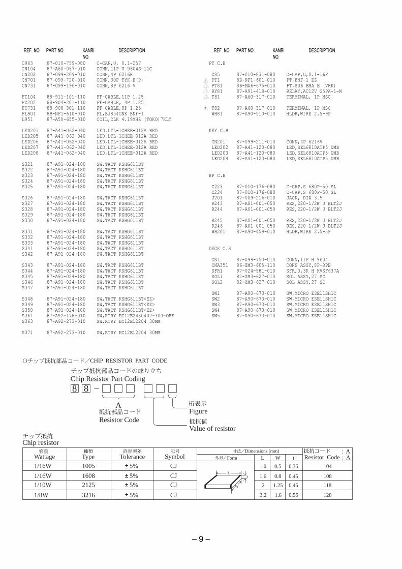
8 8
A
Resistor Code
Chip Resistor Part Coding
Figure
Value of resistor
Chip resistor
Wattage Type Tolerance
1/16W
1/10W
1/8W
1608
2125
3216
5%
5%
5%
CJ
CJ
CJ
Form L W t
1.6 0.8 0.45
2 1.25 0.45
3.2 1.6
108
118
128
: A : A
CHIP RESISTOR PART CODE
0.55
Resistor CodeDimensions (mm)
Symbol
1/16W 1005 5% CJ 1.0 0.5 0.35 104L
t
W
!
!
!
!
– 11 –
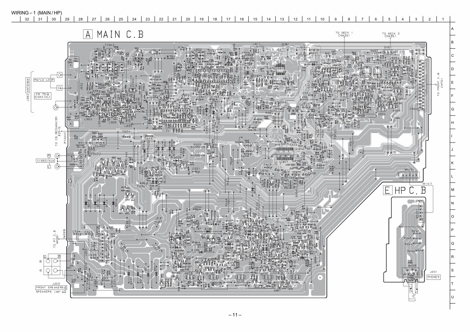
WIRING – 1 (MAIN / HP)32 31 30 29 28 27 26 25 24 23 22 21 20 19 18 17 16 15 14 13 12 11 10 9 8 7 6 5 4 3 2 1
A
B
C
D
E
F
G
H
I
J
K
L
M
N
O
P
Q
R
S
T
U
– 12 –
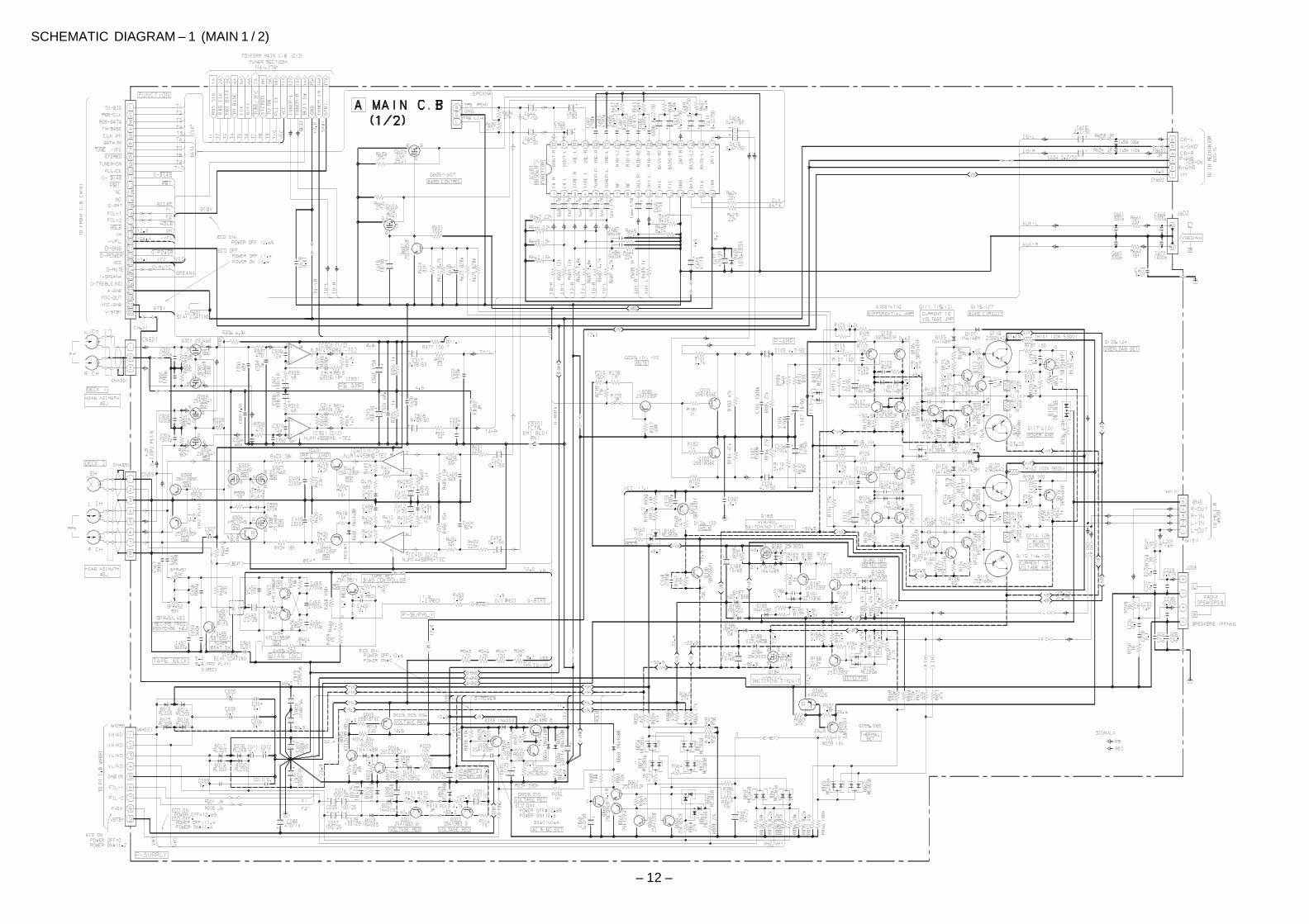
SCHEMATIC DIAGRAM – 1 (MAIN 1 / 2)
– 13 –
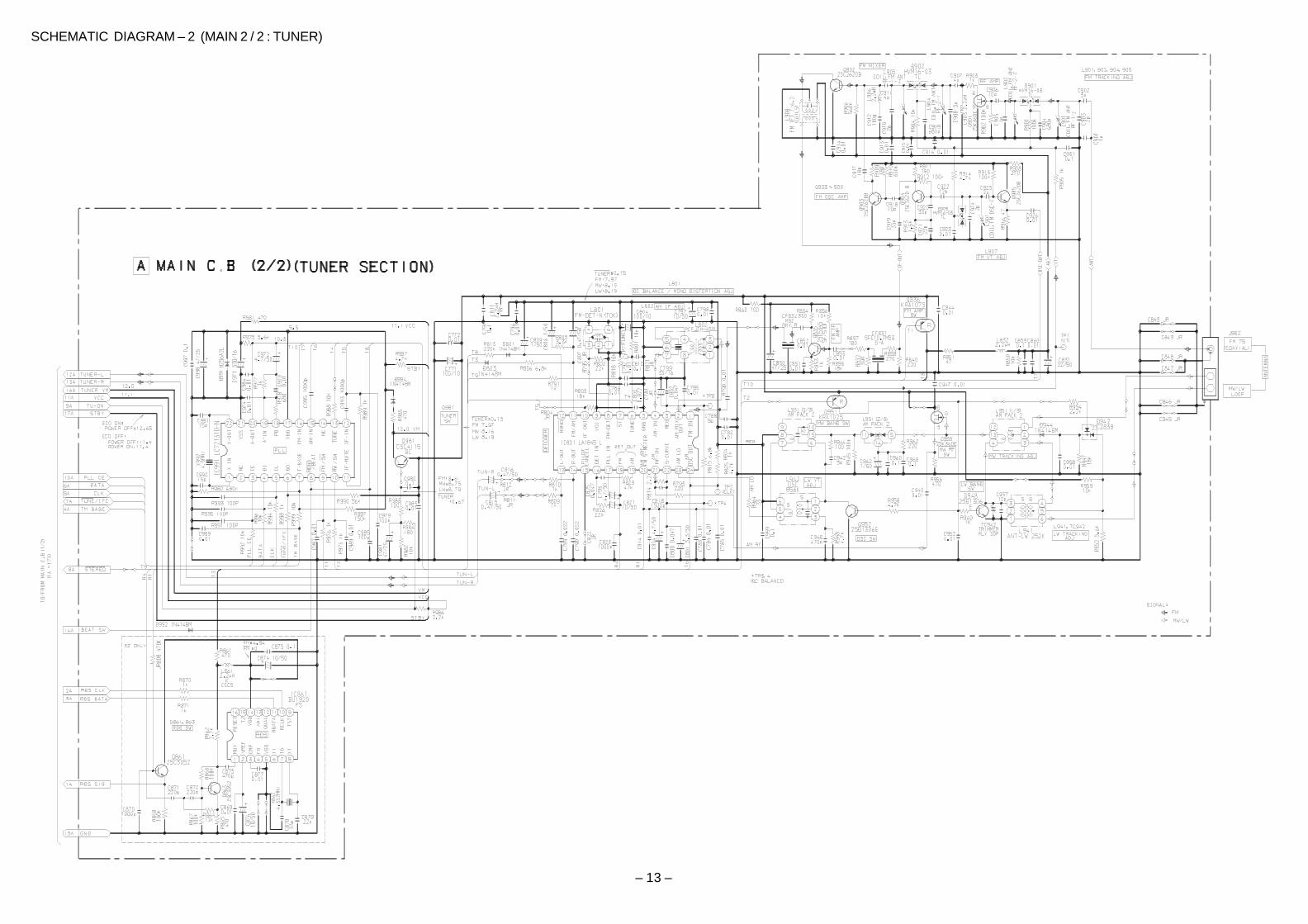
SCHEMATIC DIAGRAM – 2 (MAIN 2 / 2 : TUNER)
– 14 –
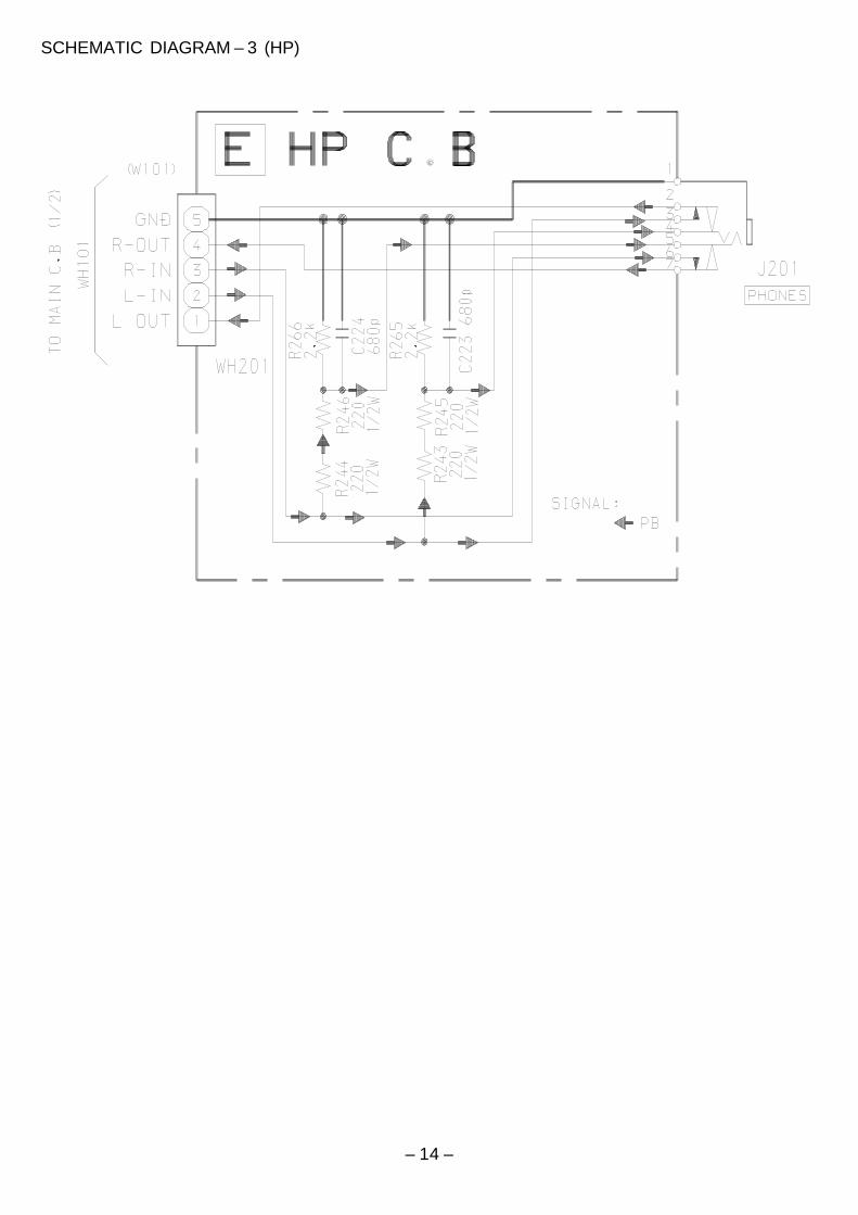
SCHEMATIC DIAGRAM – 3 (HP)
– 15 –
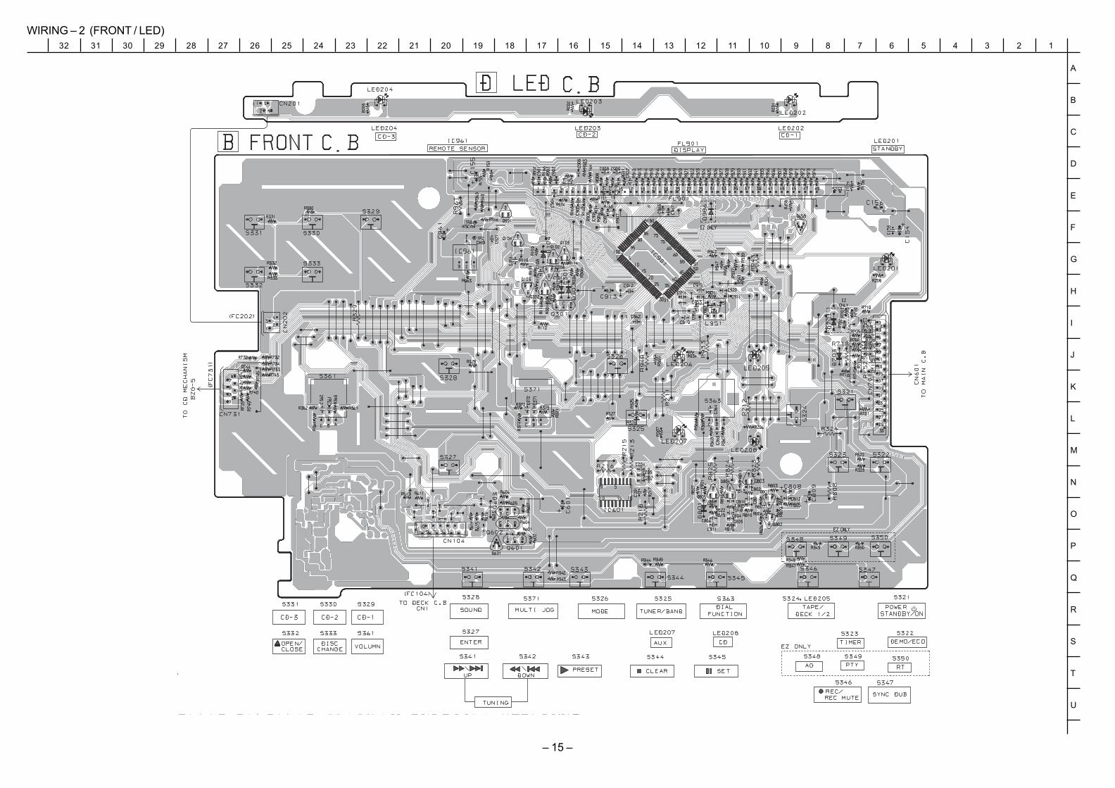
WIRING – 2 (FRONT / LED)32 31 30 29 28 27 26 25 24 23 22 21 20 19 18 17 16 15 14 13 12 11 10 9 8 7 6 5 4 3 2 1
A
B
C
D
E
F
G
H
I
J
K
L
M
N
O
P
Q
R
S
T
U
– 16 –
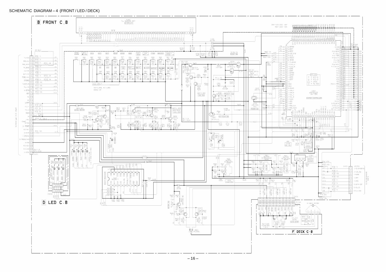
SCHEMATIC DIAGRAM – 4 (FRONT / LED / DECK)
– 17 –
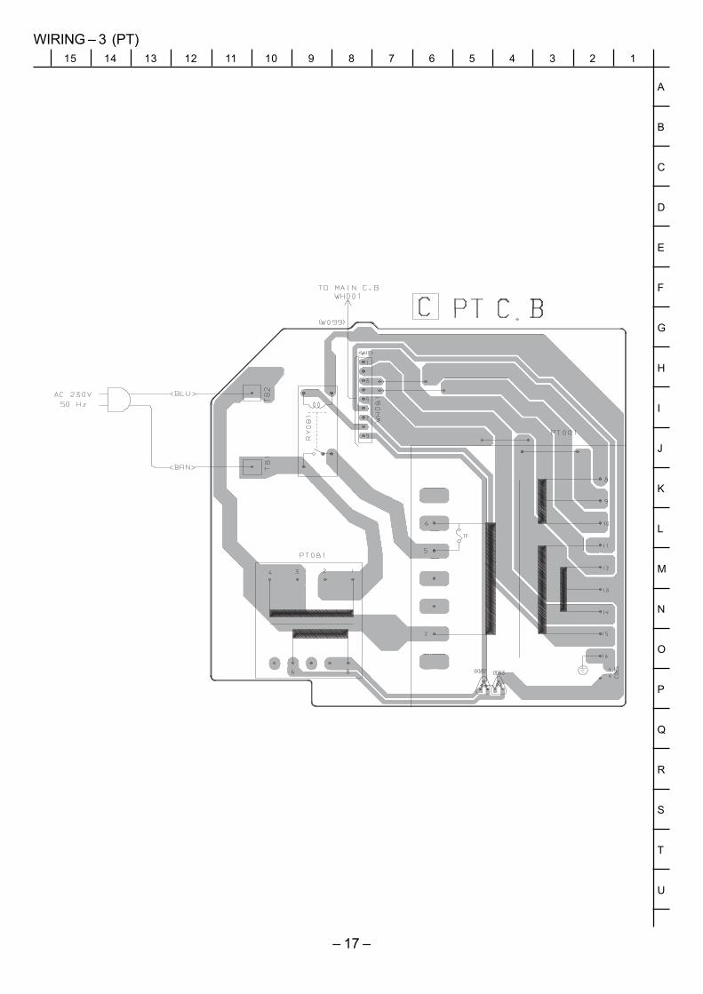
WIRING – 3 (PT)15 14 13 12 11 10 9 8 7 6 5 4 3 2 1
A
B
C
D
E
F
G
H
I
J
K
L
M
N
O
P
Q
R
S
T
U
– 18 –
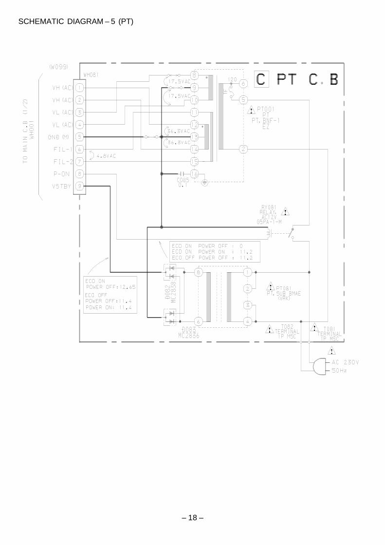
SCHEMATIC DIAGRAM – 5 (PT)
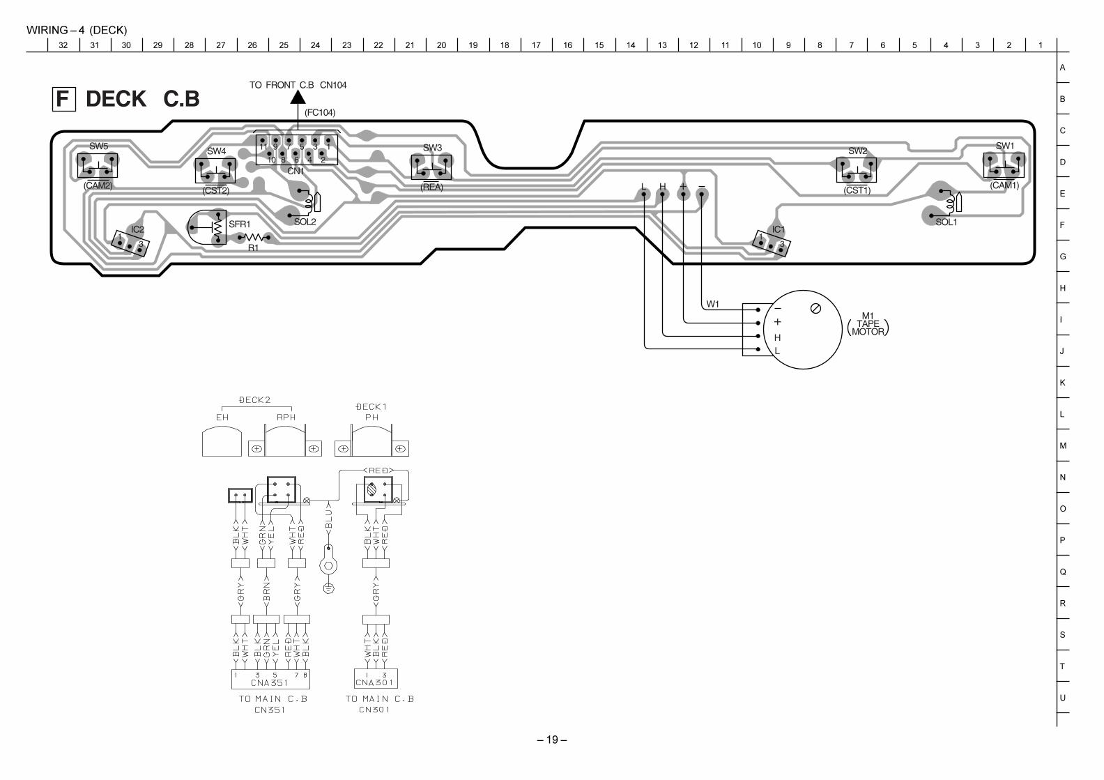
SW5
(CAM2)
SW1
(CAM1)
SOL1SOL2
SW2
(CST1)
SW3
(REA)
SW4
(CST2)
IC21
3
IC11
3
L H +
R1
SFR1
TO FRONT C.B CN104
(FC104)
CN1
11 9 7 5 3 1
10 8 6 4 2
W1M1
TAPEMOTOR
L H
+
F DECK C.B
– 20 –
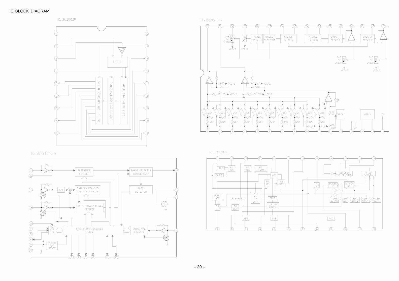
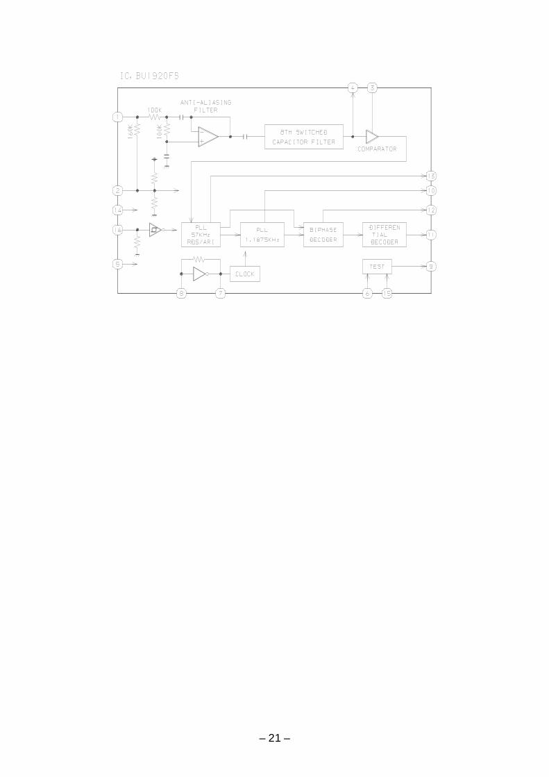
IC BLOCK DIAGRAM
– 21 –
2
– 23 –
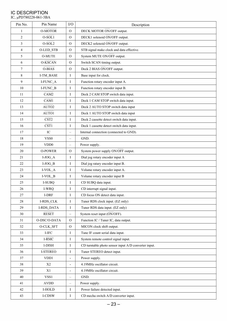
IC DESCRIPTIONIC, µPD780228-061-3BA
Pin Name I/O DescriptionPin No.
1 O-MOTOR O DECK MOTOR ON/OFF output.
2 O-SOL1 O DECK1 solenoid ON/OFF output.
3 O-SOL2 O DECK2 solenoid ON/OFF output.
4 O-LED_STB O STB signal make clock and data effective.
5 O-MUTE O System MUTE ON/OFF output.
6 O-KSCAN O Switch SCAN timing output.
7 O-BIAS O Deck 2 BIAS ON/OFF output.
8 I-TM_BASE I Base input for clock.
9 I-FUNC_A I Function rotary encoder input A.
10 I-FUNC_B I Function rotary encoder input B.
11 CAM2 I Deck 2 CAM STOP switch data input.
12 CAM1 I Deck 1 CAM STOP switch data input.
13 AUTO2 I Deck 2 AUTO STOP switch data input
14 AUTO1 I Deck 1 AUTO STOP switch data input
15 CST2 I Deck 2 cassette detect switch data input.
16 CST1 I Deck 1 cassette detect switch data input.
17 IC – Internal connection (connected to GND).
18 VSS0 – GND.
19 VDD0 – Power supply.
20 O-POWER O System power supply ON/OFF output.
21 I-JOG_A I Dial jog rotary encoder input A
22 I-JOG_B I Dial jog ratary encoder input B.
23 I-VOL_A I Volume rotary encoder input A.
24 I-VOL_B I Volume rotary encoder input B
25 I-SUBQ I CD SUBQ data input.
26 I-WRQ I CD interrupt signal input.
27 I-DRF I CD focus ON detect data input.
28 I-RDS_CLK I Tuner RDS clock input. (EZ only)
29 I-RDS_DATA I Tuner RDS data input. (EZ only)
30 RESET – System reset input (ON/OFF).
31 O-DSC/O-DATA O Function IC / Tuner IC, data output.
32 O-CLK_SFT O MICON clock shift output.
33 I-IFC I Tune IF count serial data input.
34 I-RMC I System remote control signal input.
35 I-DISH I CD turntable photo sensor input A/D converter input.
36 I-STEREO I Tuner STEREO detect input.
37 VDD1 - Power supply.
38 X2 - 4.19MHz oscillator circuit.
39 X1 - 4.19MHz oscillator circuit.
40 VSS1 – GND.
41 AVDD – Power supply.
42 I-HOLD I Power failure detected input.
43 I-CDSW I CD mecha switch A/D converter input.
– 24 –
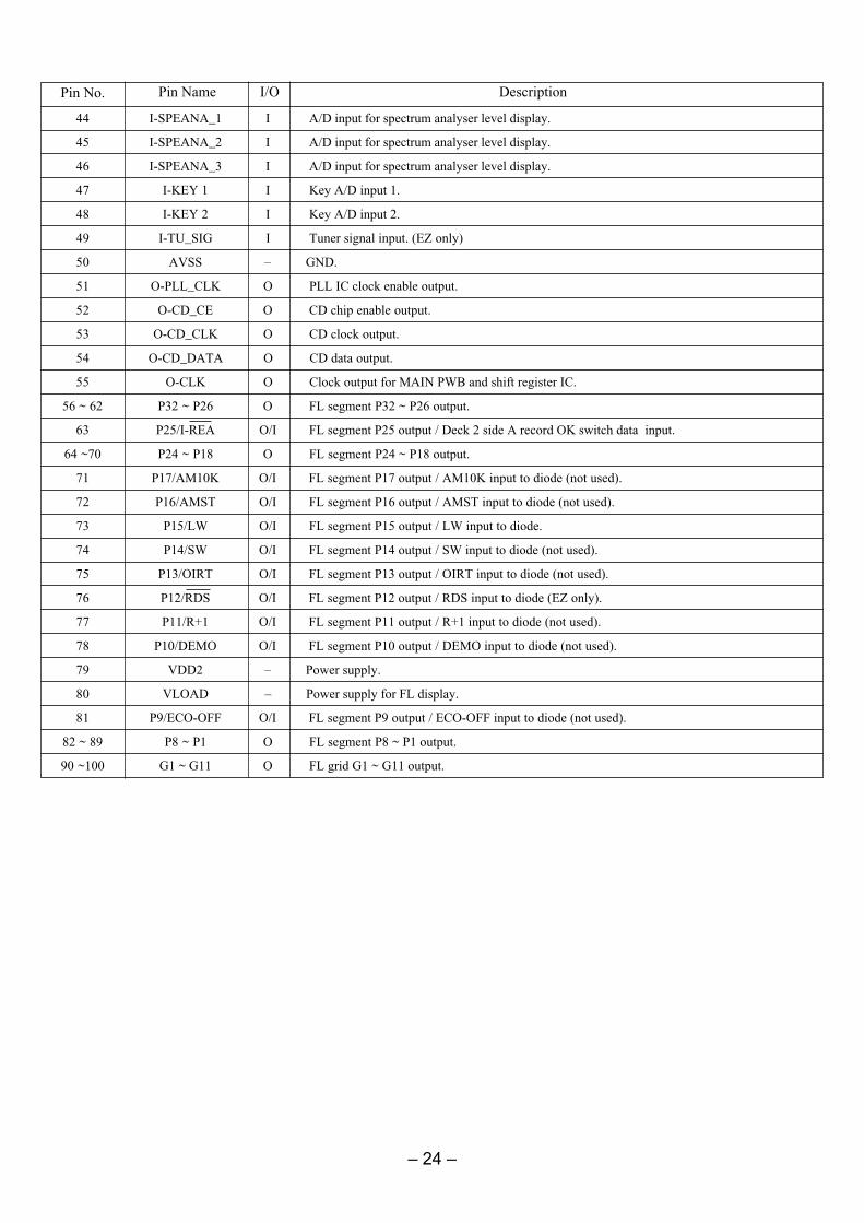
Pin Name I/O DescriptionPin No.
44 I-SPEANA_1 I A/D input for spectrum analyser level display.
45 I-SPEANA_2 I A/D input for spectrum analyser level display.
46 I-SPEANA_3 I A/D input for spectrum analyser level display.
47 I-KEY 1 I Key A/D input 1.
48 I-KEY 2 I Key A/D input 2.
49 I-TU_SIG I Tuner signal input. (EZ only)
50 AVSS – GND.
51 O-PLL_CLK O PLL IC clock enable output.
52 O-CD_CE O CD chip enable output.
53 O-CD_CLK O CD clock output.
54 O-CD_DATA O CD data output.
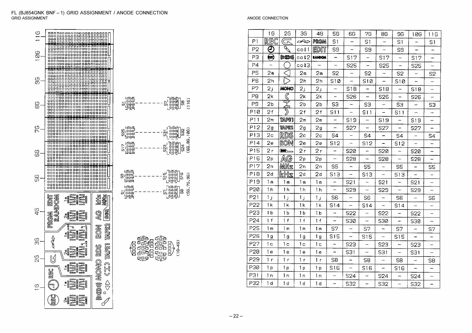
55 O-CLK O Clock output for MAIN PWB and shift register IC.
56 ~ 62 P32 ~ P26 O FL segment P32 ~ P26 output.
63 P25/I-REA O/I FL segment P25 output / Deck 2 side A record OK switch data input.
64 ~70 P24 ~ P18 O FL segment P24 ~ P18 output.
71 P17/AM10K O/I FL segment P17 output / AM10K input to diode (not used).
72 P16/AMST O/I FL segment P16 output / AMST input to diode (not used).
73 P15/LW O/I FL segment P15 output / LW input to diode.
74 P14/SW O/I FL segment P14 output / SW input to diode (not used).
75 P13/OIRT O/I FL segment P13 output / OIRT input to diode (not used).
76 P12/RDS O/I FL segment P12 output / RDS input to diode (EZ only).
77 P11/R+1 O/I FL segment P11 output / R+1 input to diode (not used).
78 P10/DEMO O/I FL segment P10 output / DEMO input to diode (not used).
79 VDD2 – Power supply.
80 VLOAD – Power supply for FL display.
81 P9/ECO-OFF O/I FL segment P9 output / ECO-OFF input to diode (not used).
82 ~ 89 P8 ~ P1 O FL segment P8 ~ P1 output.
90 ~100 G1 ~ G11 O FL grid G1 ~ G11 output.
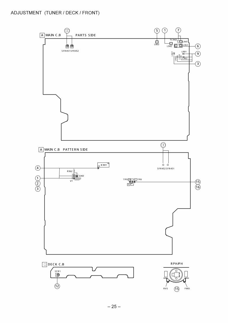
SFR1
12
G DECK C.B
A MAIN C.B
15RVS FWD
RPH/PH
A MAIN C.B PATTERN SIDE
TC942
R L
G
SFR452SFR451
SFR451SFR452
IC80124
5 1 7
L942 L951L802
L901
L902
L9
07
L9
05
L9
04
L941
6
9
15
5PARTS SIDE
1
4
2
3
R962
VT
GND
TP8TP9
16
3
5
RO
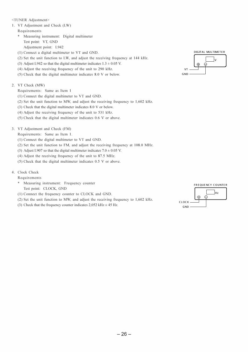
! " # $ %# &&
'( $ )*%
'( $ +,-
( # && ( *%
- . / ( ( ) 0# / 1 ,, 23
4 +,-( # && 45667
, 0# / 1 (/ ( -+6 23
7 # && 86 ( 9&(:
- "
$ . ;
( # && ( *%
- . / ( (") 0# / 1 ( )<6- 23
4 # && 86( 9&(:
, 0# / 1 (/ ( 74 23
7 # && 6< ( 9(0
4 ="
$ . ;
( # && ( *%
- . / ( ( =") 0# / 1 686"23
4 +6>( # && >65667
, 0# / 1 (/ ( 8>7"23
7 # && 67 ( 9(0
, &(
! " # $ = 1 (
'( $ ?@)*%
( / 1 ( ( ?@ *%
- . / ( (") 0# / 1 ( )<6- 23
4 / 1( -)67-235,723
V
DIGITAL MULTIMETER
VT
GND
Hz
FREQUENCY COUNTER
CLOCK
GND
"A
" /(&&(:# # ( 9/(
B ' (
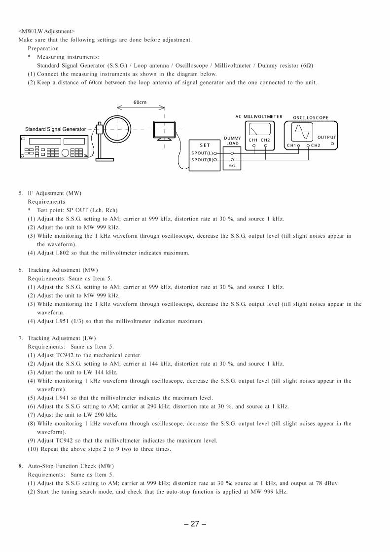
! " # $
. .#&* ( ..* A ((' A ?&&((' A"&&0(& A %1 ( <Ω
( # (: # 9&(:
- @' (/ <6 9 : &((' (/ #& # ( ( ( (
DUMMY
SPOUT(L)
AC MILLIVOLTMETER
CH2CH1
6Ω
OUTPUT
OSCILLOSCOPE
CH2CH1LOAD
60cm
SET
Standerd Signal Genertaor
SPOUT(R)
7 ;= "
! '( $ .B? )
..* # ("C +++ 23) ( ( 46D) ( 23
- ("+++ 23
4 &( ( # 23:0/( (# (&&((') ..* ( ' &0& && &# ( ''
:0/(
, 86- ( &&0(& E
< # "
$ . ; 7
..* # ("C +++ 23) ( ( 46D) ( 23
- ("+++ 23
4 &( ( # 23:0/( (# (&&((') ..* ( ' &0& && &# ( ''
:0/(
, +7 A4 ( &&0(& E
> #
$ . ; 7
+,- ( &
- ..* # ("C ,, 23) ( ( 46D) ( 23
4 (,, 23
, &( ( # 23:0/( (# (&&((') ..* ( ' &0& && &# ( ''
:0/(
7 +, ( &&0(& E &0&
< ..* # ("C -+6 23C ( ( 46D) ( 23
> (-+6 23
8 &( ( # 23:0/( (# (&&((') ..* ( ' &0& && &# ( ''
:0/(
+ +,- ( &&0(& E &0&
6 ' 9(0 ' - ( + :( (
8 (F. (' = ( "
$ . ; 7
..* # ("C +++ 23C ( ( 46DC ( 23) ( ' >8 G0
- . # () (F (' / ( ''& "+++ 23
="
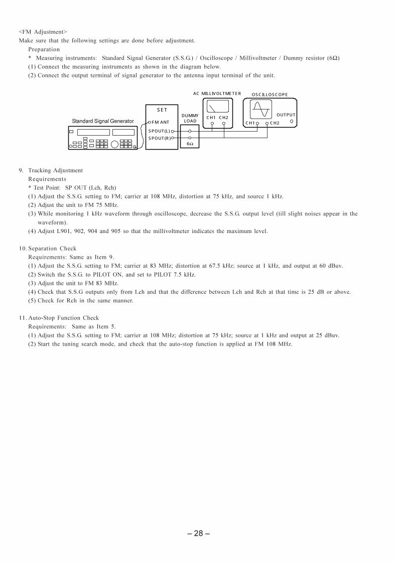
" /(&&(:# # ( 9/(
B ' (
! " # $ . .#&* ( ..* A ?&&((' A"&&0(& A %1 ( <Ω
( # (: # 9&(:
- ( ( ' & (/ #& # ( ( ' & (/
DUMMY
SPOUT(L)
AC MILLIVOLTMETER
CH2CH1
6Ω
OUTPUT
OSCILLOSCOPE
CH2CH1LOAD
SET
Standerd Signal Genertaor FM ANT
SPOUT(R)
+ #
! B( $ .B? )
..* # ( ="C 68"23) ( ( >7 23) ( 23
- (=">7"23
4 &( ( # 23:0/( (# (&&((') ..* ( ' &0& && &# ( ''
:0/(
, +6) +6-) +6, +67 ( &&0(& E &0&
6 .' (
$ . ; +
..* # ( ="C 84"23C ( ( <>7 23C ( 23) ( ' <6 G0
- .: ..* ( B;??) ( B;? >7 23
4 (="84"23
, ..* ( ' (&1 / ( // 9 : -7 G ( 9(0
7 /(
(F. (' = (
$ . ; 7
..* # ( ="C 68"23C ( ( >7 23C ( 23 ( ' -7 G0
- . # () (F (' / ( ''& =" 68"23
% . (
- ' .' %@ -
! " # $ (:F/& / 1 (
'$ F66 4 23
'( $ 2B?
'( $ .=
( 2B? & (/ ( :(:F/&
- ; ' F66 (%@- B&19 & ' (/ '
=% () .=( &0&)4)6662357239(9
4 B&19 . ( #: 5,723(9 #
=%'
4 ' .' %@
$ . ;
; ' F66 (%@ B&19 & ' (/ ')
#: 57723(9 # '(/%@-
,(:F=& %@)%@-
$ . ;
( 2B? & (/ ( :(:F/&
- .: :(:F/& # / ( ;%;? ( H;.) / ( ( (".
%
4 B&19 & ' (/ ' F66) &0& 6-D
( 9&(:
723 %@)%@-
! " # $ ?&&(('
'$ F466 6 23
'( $ B8 )B+
'( $ 2 3 :
( 2 (/ (&&((' ' (9 (B8 2- (B+
- . ( (/ (&&((' (%%
4 ; ' F466 (%@ B&19 & ' (/ '
=% () 3 : ( :0/(
E: 6 23 '&1
, ' (0 ) '&19 . ( 3
: ( :0/( (/ (&&((' 9(E
7 / ) &( : 91 9(# <66G
< ''&1 9(0 ' 4 ( 7 (%@-
< B&19 = 1 %@ )%@ -
! " # $ "&&0(&
'$ F466 4723 A 6 23
'( $ B8 )B+
( 2 (/&&0(& (B8 2- ( B+
- ; ' F446 (%@ ) '&19 4723 6 23
4 623&0& #: 54G(' ( ( ' /
&0&(/4723
, ''&1 9(0 '-4 (%@-
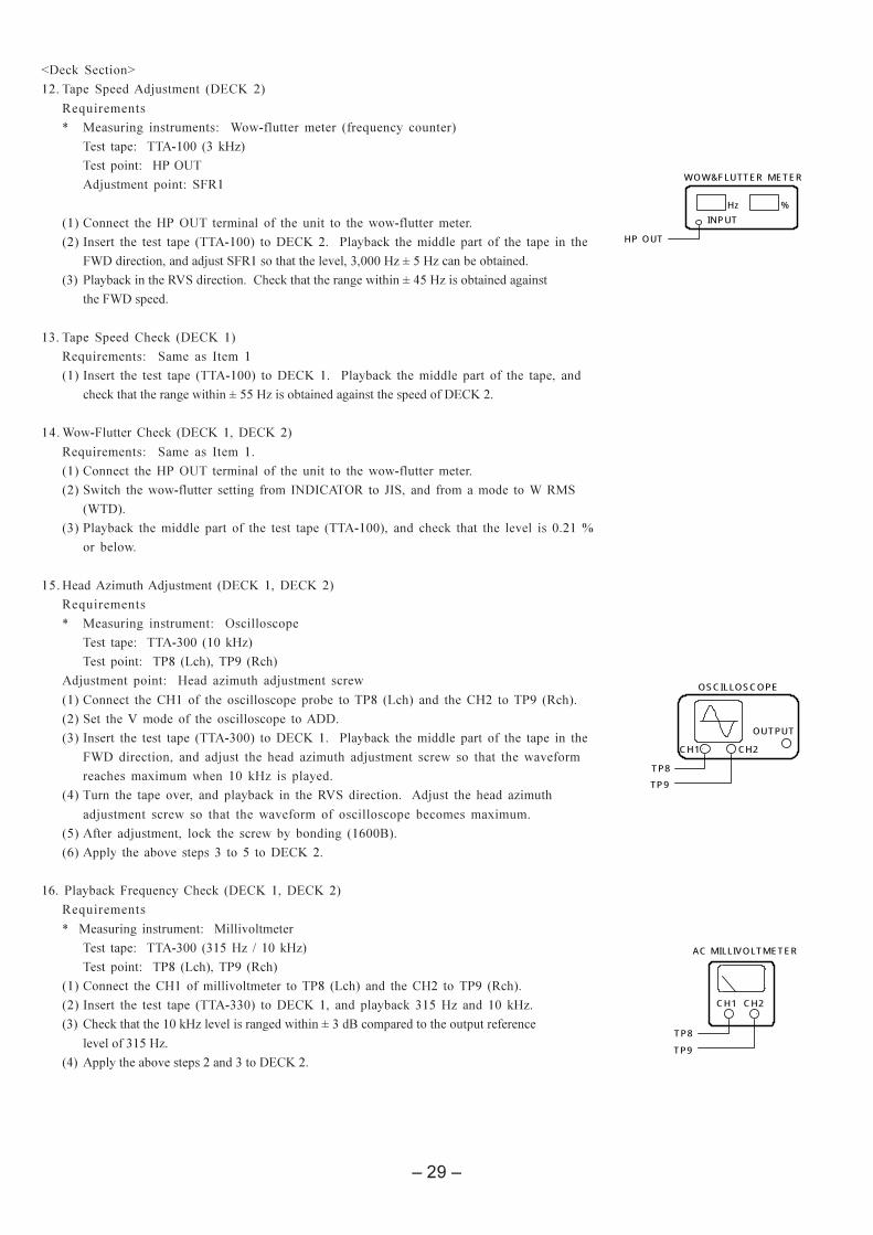
Hz
WOW&FLUTTER METER
HP OUT
%
INPUT
OUTPUT
OSCILLOSCOPE
TP8
TP9
CH1 CH2
TP8
TP9
AC MILLIVOLTMETER
CH2CH1
> B&19 . 0 1 %@)%@-
! " # $ "&&0(&
'$F-66 ,6623
'( $ B8 )B+
( 2 (/&&0(& (B8 2- ( B+
- ; ' F-66 (%@ ( '&19
4 ( ' &0& #: 66654G
, ''&1 9(0 ' - 4 (%@-
8 B&19A( = 1 '( %@ -
! " # $ "&&0(&
( #& (&& ( &(:F/ 1 (&& (
(
'$ F<6- ?"
'( $ B8 )B+
;' '( $ I23 A823
'( $ .=,7 ) .=,7-
( 2 (/&&0(& ( B8 2 (B+
- ( ( ' & (/ (&& ( ( ( ) ( (I (/
4 ; ' F<6- (%@-) ( 23 #& /( I
, ( ( ( ' &0& (/B8 B+ 9( 86
7 ( 23 8 23 & &1
< .=,7.=,7-( '&19( ' &0&(/823 #: 6567G(' (
'&19( ' / &0&(/23
+ B&19A( . 0 1 %@ -
! " # $ . ; 8
'$F<6- ?"
'( $B8 ) B+
;' '( $I 23
; ' F<6- (%@-) ( 23 #& / (I
- ( ( ( ' &0& (/B8 B+ 9( 866
4 B&1923) ( ' &0& #: FG547G(' ( ( ' &0& # ( #
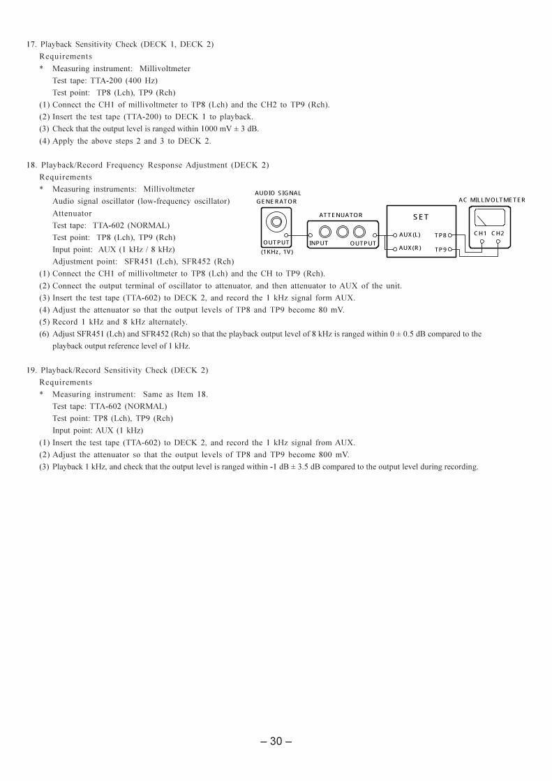
ATTENUATOR
INPUT OUTPUT
AUX(L)
AUX(R)OUTPUT
AUDIO SIGNAL
GENERATOR
TP8
TP9
AC MILLIVOLTMETER
CH2CH1
SET
(1KHz, 1V)
-6 &(
! " # $ = 1 (
'( $ ?@)*%
& ' # (&# (: B? 9 ( B 9 () '&#
- +7( / 1( 8,86,5668,23
Hz
FREQUENCY COUNTER
CLOCK
GND
1CLOCK
GND
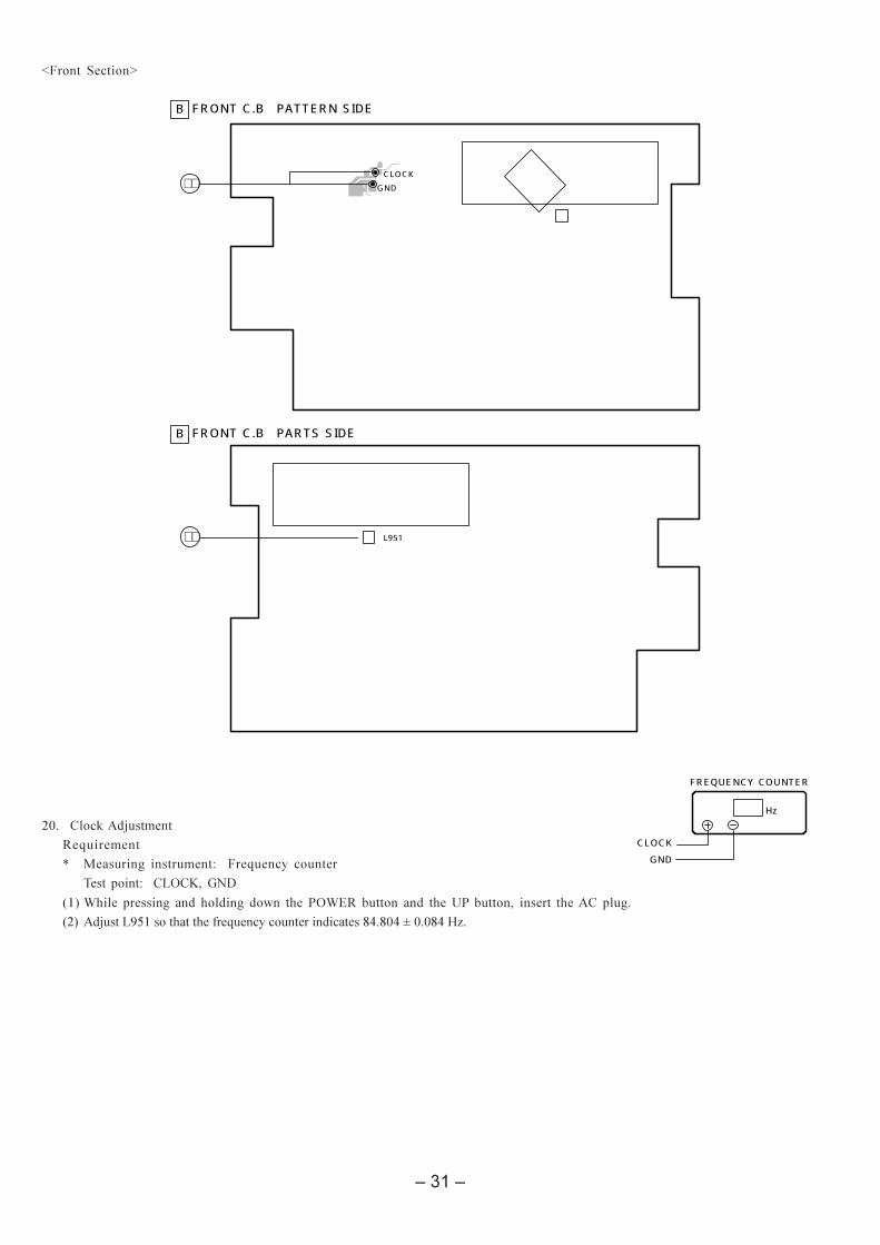
L9511
B FRONT C.B PATTERN SIDE
B FRONT C.B PARTS SIDE
= ( . (
!"#$%&' (
) * !+
, -.#
! " #$%& !' ' ( )
*+(
*+( ,# - - .
/ ! !0" # " + ( # '#$ +"
1 + !2$ " # - +3 - " 3 + !2$ "
4 " ' $ !2+ )5 -
( !2
6 " ' $ !2+ )5
7 #$'3#$' 6 " 2 $ " (5
6 , - . 5 + 5
) 6 ( 85 + %' - 5 +- % 5 (( *5 + ( *5 5
) 6 5 " #6 " *5 (5 "+ - + -
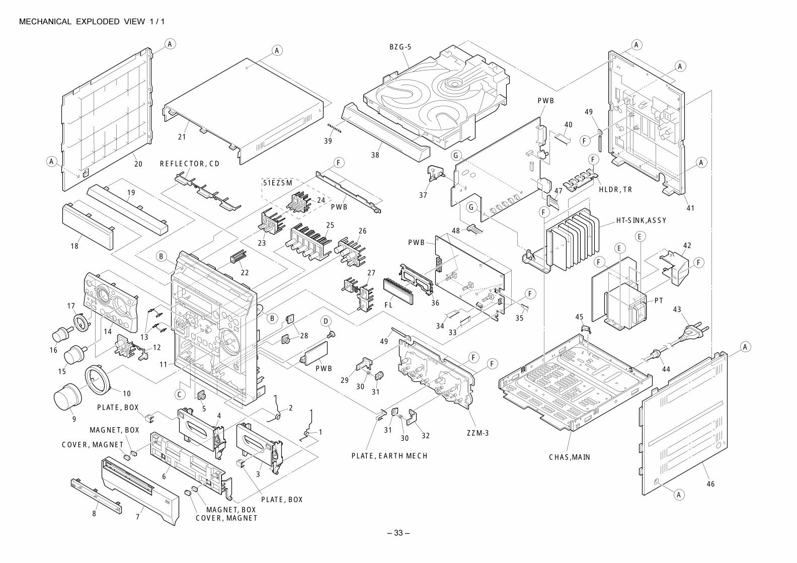
33
0.00.20.40.60.81.0
PLATE, EARTH MECH
MAGNET, BOX
MAGNET, BOX
PLATE, BOX
REFLECTOR, CD
PLATE, BOX
COVER, MAGNET
COVER, MAGNET
7
6 3
45
1
2
8
9
10
11
1213
14
15
16
17
18
19
20
21
22
23
24
2526
27
28
29
32
3334
49
35
36
37
38
39
40
49
47
48
41
42
43
44
45
46
30
30
31
31
CHAS,MAIN
ZZM-3
F
F
F
F
F
F
B D
B
F
A
E
E
FF
A
PWB
PWB
PWB
51EZSM
PWB
A
G
C
G
BZG-5AA
A
A
A
HT-SINK,ASSY
PT
HLDR, TR
FL
34
!
! " " # #$
# #$ % %! % %!
& & $
& &
%& &%! & &
' '( $
& & $ & #
!" ##
!$%!"$"%" &$%
"$"%" '" &!&!!$%
!!"$"%!
" " $%" " "
!("" "("
)))'&!)(
'!!#)*#+!$%!"$"%
( "&(!'*+(!'(
))!!& ,-". ,'
# , ,! , !'# ,'! ,&
35
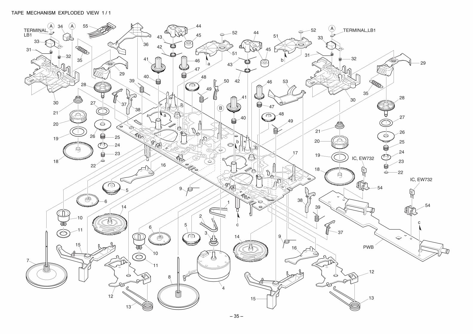
A TERMINAL,LB1A A
B
TERMINAL,LB1
1
2
3
4
5
5
6
6
7
8
9
9
10
11
10
11
12
12
13
13
14
14
15
15
16
16
18
18
19
19
20
20
21
21
30
22
23
24
2526
27
28
22
23
24
25
26
27
28
29
31
32
33
34
35
36
37
37
38
38
39
39
40
41
42
43
44
51
5245
46
47
48
49
50 53
54
54
17
55
3035
29
3132
33
5251
44
45
43
42
IC, EW732
IC, EW732
ba
a
b
c c
40
41
46
47
48
49
PWB
36
!"! #"
!! $#"! $
!# $"" #!
" %"!" !"
! !# # $ $
"##$# #
! $&" $ $"# $""
" $"! "
!! " #! $"'()
! $ %!% $&" "!!"
" !%$*%!
– 37 –
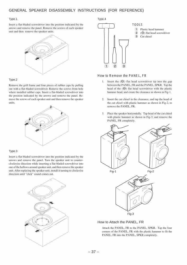
GENERAL SPEAKER DISASSEMBLY INSTRUCTIONS (FOR REFERENCE)
Insert a flat-bladed screwdriver into the position indicated by thearrows and remove the panel. Remove the screws of each speakerunit and then remove the speaker units.
Type.1
Type.3
Type.2
Type.4
Fig-1 Fig-2
Fig-3
How to Attach the PANEL, FR
Attach the PANEL, FR to the PANEL, SPKR. Tap the fourcorners of the PANEL, FR with the plastic hammer to fit thePANEL, FR into the PANEL, SPKR completely.
1 2 3
Insert a flat-bladed screwdriver into the position indicated by thearrows and remove the panel. Turn the speaker unit to counter-clockwise direction while inserting a flat-bladed screwdriver intoone of the hollows around speaker unit, and then remove the speakerunit. After replacing the speaker unit, install it turning to clockwisedirection until "click" sound comes out.
Remove the grill frame and four pieces of rubber caps by pullingout with a flat-bladed screwdriver. Remove the screws from holewhere installed rubber caps. Insert a flat-bladed screwdriver intothe position indicated by the arrows and remove the panel. Re-move the screws of each speaker unit and then remove the speakerunits.
TOOLS
1 Plastic head hammer2 (() flat head screwdriver3 Cut chisel
How to Remove the PANEL, FR
1. Insert the (() flat head screwdriver tip into the gapbetween the PANEL, FR and the PANEL, SPKR. Tap thehead of the (() flat head screwdriver with the plastichammer head, and create the clearance as shown in Fig-1.
2. Insert the cut chisel in the clearance, and tap the head ofthe cut chisel with plastic hammer as shown in Fig-2, toremove the PANEL, FR.
3. Place the speaker horizontally. Tap head of the cut chiselwith plastic hammer as shown in Fig-3, and remove thePANEL, FR completely.
– 38 –
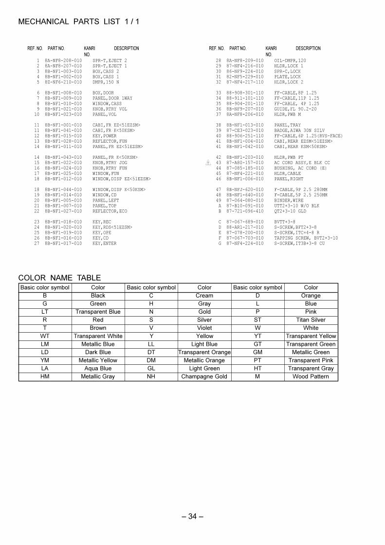
DESCRIPTIONREF. NO. KANRINO.
PART NO.
SPEAKER PARTS LISTSX-NR50 (YSL)
1 8B-NSA-001-010 PANEL,FR R 2 8B-NSA-002-010 PANEL,FR L 3 8B-NSA-003-010 PANEL,BA R 4 8B-NSA-004-010 PANEL,BA L 5 8B-NSA-005-010 GRILLE,FRAME ASSY
6 8B-NSA-602-010 SPKR, W 160 30/4 7 8B-NSK-604-010 SPKR, T 60 8 88-NSK-610-010 SPKR, CERAMIC ASSY
ACCESSORIES / PACKAGE LIST
DESCRIPTIONREF. NO. KANRINO.
PART NO.
1 8B-NF1-905-010 IB,K(E)M<K> 1 8B-NF1-906-010 IB,EZ(9L)M<EZ> 2 87-A90-118-010 ANT,WIRE FM<EZ> 3 87-006-268-010 ANT LOOP,AM 4 8B-NF1-701-010 RC UNIT,CAS01
5 87-099-811-010 PLUG, ADPTR CONV(K)<K>!

2–11, IKENOHATA 1–CHOME, TAITO-KU, TOKYO 110, JAPAN TEL:03 (3827) 3111
Printed in Singapore9301978 9720501 921338