Embed Size (px)
Citation preview
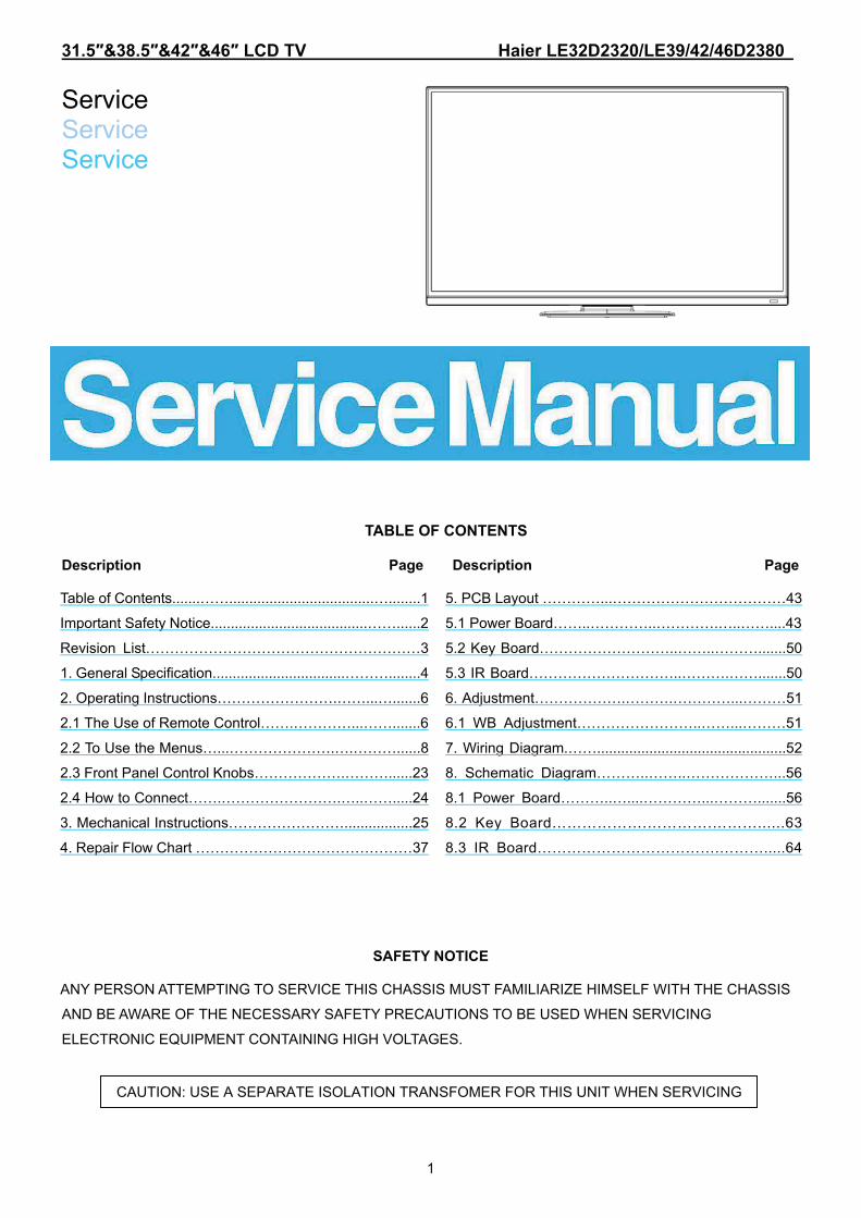
31.5�&38.5�&42�&46� LCD TV Haier LE32D2320/LE39/42/46D2380
1
Service Service Service
TABLE OF CONTENTS
Description Page Description Page
SAFETY NOTICE ANY PERSON ATTEMPTING TO SERVICE THIS CHASSIS MUST FAMILIARIZE HIMSELF WITH THE CHASSIS
AND BE AWARE OF THE NECESSARY SAFETY PRECAUTIONS TO BE USED WHEN SERVICING
ELECTRONIC EQUIPMENT CONTAINING HIGH VOLTAGES.
5. PCB Layout …………...………………………………43
5.1 Power Board……..…………..………….…..……....43
5.2 Key Board………………………..……..……….......50
5.3 IR Board…………………………..……….…….......50
6. Adjustment……………….……….…………...………51
6.1 WB Adjustment……………………..……...………51
7. Wiring Diagram.……...............................................52
8. Schematic Diagram………..……..………………...56
8.1 Power Board………..…....…………...……….......56
8.2 Key Board……………….………….………......63
8.3 IR Board……………………………….……….....64
Table of Contents.......……....................................…........1
Important Safety Notice.......................................……......2
Revision List…………………………………………………3
1. General Specification.................................………........4
2. Operating Instructions…………………….……...….......6
2.1 The Use of Remote Control…….…………...…….......6
2.2 To Use the Menus…...………………….….………......8
2.3 Front Panel Control Knobs……………….………......23
2.4 How to Connect…….…………………….…..…….....24
3. Mechanical Instructions…………………….................25
4. Repair Flow Chart ………………………………………37
CAUTION: USE A SEPARATE ISOLATION TRANSFOMER FOR THIS UNIT WHEN SERVICING
2
Important Safety Notice Proper service and repair is important to the safe, reliable operation of all Haier Company Equipment. The service procedures recommended by Haier and described in this service manual are effective methods of performing service operations. Some of these service operations require the use of tools specially designed for the purpose. The special tools should be used when and as recommended.
It is important to note that this manual contains various CAUTIONS and NOTICES which should be carefully read in order to minimize the risk of personal injury to service personnel. The possibility exists that improper service methods may damage the equipment. It is also important to understand that these CAUTIONS and NOTICES ARE NOT EXHAUSTIVE. Haier could not possibly know, evaluate and advise the service trade of all conceivable ways in which service might be done or of the possible hazardous consequences of each way. Consequently, Haier has not undertaken any such broad evaluation. Accordingly, a servicer who uses a service procedure or tool which is not recommended by Haier must first satisfy himself thoroughly that neither his safety nor the safe operation of the equipment will be jeopardized by the service method selected. Hereafter throughout this manual, Haier Company will be referred to as Haier. WARNING Use of substitute replacement parts, which do not have the same, specified safety characteristics might create shock, fire, or other hazards. Under no circumstances should the original design be modified or altered without written permission from Haier. Haier assumes no liability, express or implied, arising out of any unauthorized modification of design. Servicer assumes all liability. FOR PRODUCTS CONTAINING LASER: DANGER-Invisible laser radiations when open AVOID DIRECT EXPOSURE TO BEAM. CAUTION-Use of controls or adjustments or performance of procedures other than those specified herein may result in hazardous radiation exposure. CAUTION -The use of optical instruments with this product will increase eye hazard. TO ENSURE THE CONTINUED RELIABILITY OF THIS PRODUCT, USE ONLY ORIGINAL MANUFACTURER'S REPLACEMENT PARTS, WHICH ARE LISTED WITH THEIR PART NUMBERS IN THE PARTS LIST SECTION OF THIS SERVICE MANUAL. Take care during handling the LCD module with backlight unit -Must mount the module using mounting holes arranged in four corners. -Do not press on the panel, edge of the frame strongly or electric shock as this will result in damage to the screen. -Do not scratch or press on the panel with any sharp objects, such as pencil or pen as this may result in damage to the panel. -Protect the module from the ESD as it may damage the electronic circuit (C-MOS). -Make certain that treatment person’s body is grounded through wristband. -Do not leave the module in high temperature and in areas of high humidity for a long time. -Avoid contact with water as it may a short circuit within the module. -If the surface of panel becomes dirty, please wipe it off with a soft material. (Cleaning with a dirty or rough cloth may damage the panel.)
3
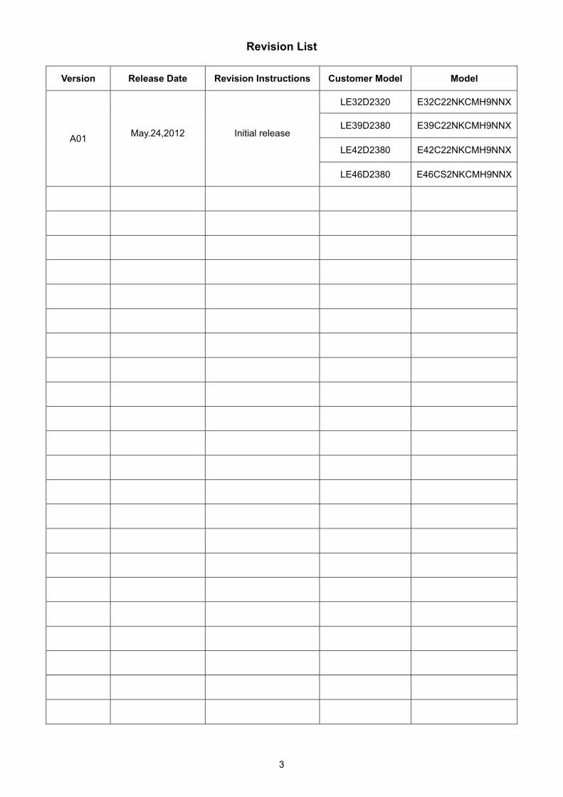
Revision List
Version Release Date Revision Instructions Customer Model Model
A01 May.24,2012
Initial release
LE32D2320 E32C22NKCMH9NNX
LE39D2380 E39C22NKCMH9NNX
LE42D2380 E42C22NKCMH9NNX
LE46D2380 E46CS2NKCMH9NNX
4
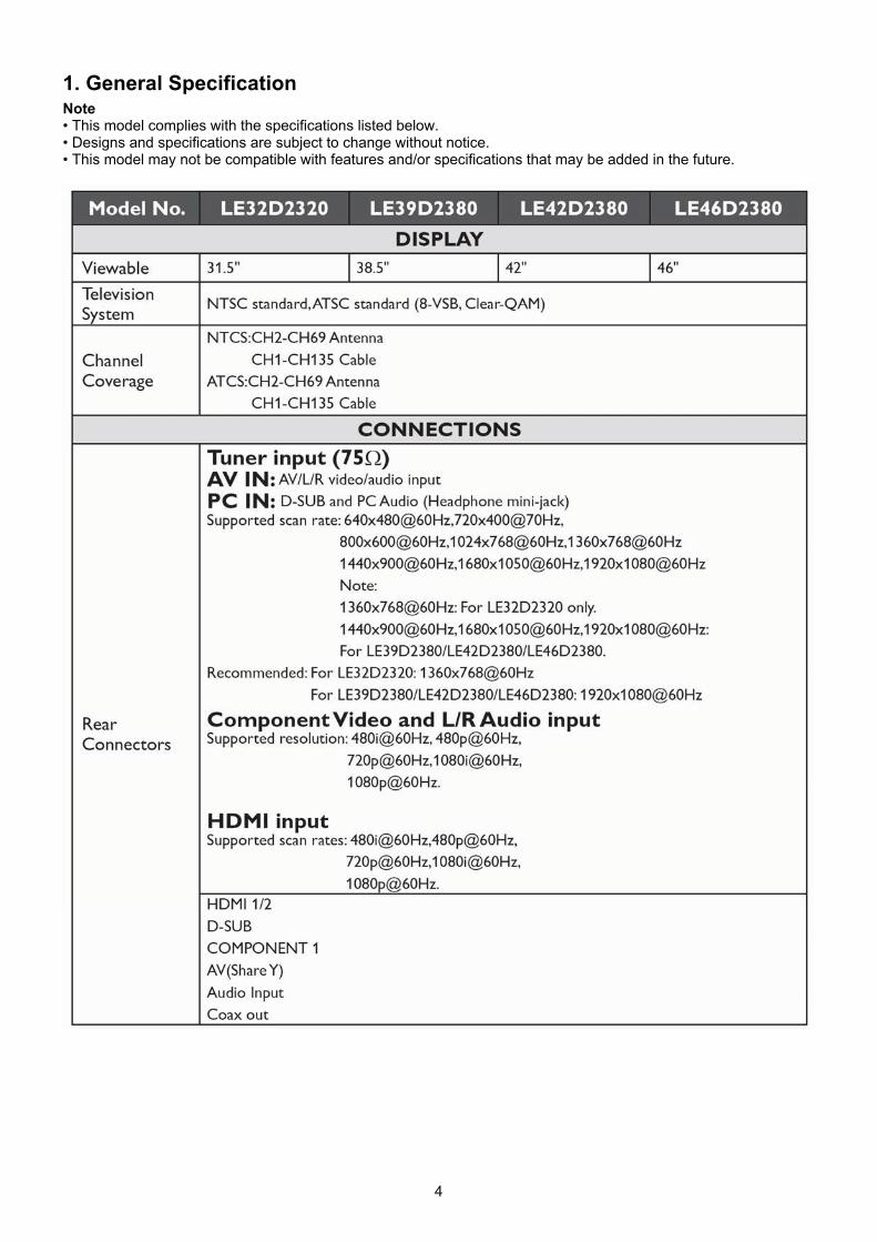
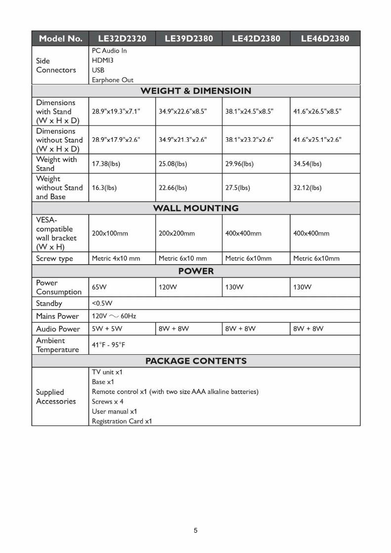
1. General Specification Note • This model complies with the specifications listed below. • Designs and specifications are subject to change without notice. • This model may not be compatible with features and/or specifications that may be added in the future.
5
6
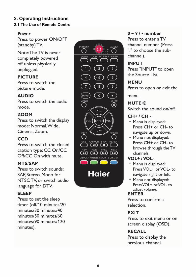
2. Operating Instructions
2.1 The Use of Remote Control
7

8
2.2 To Use the Menus Initial SetupWelcome to use the wizard for initial Setup!!Please press [ENTER] to start the wizard.
LanguagePlease select your language, press [CH-]/[CH+] to select, press [ENTER] to confirm:
Time ZonePlease select your time zone, press [CH-]/[CH+] to select, press [ENTER] to confirm:

9
Tuner TypePlease select your tuner type, press [CH-]/[CH+]to select, press [ENTER] to confirm:
Antenna: Set the signal type to antenna. When set to Air, the TV can receive analog and digital (ATSC) broadcasting
signals.2. Cable: Set the signal type to cable. When set to Cable, the TV can receive analog and QAM broadcasting
signals.ScanPlease select scan or skip scan, press [CH-]/[CH+] to select, press [ENTER] to confirm:
10
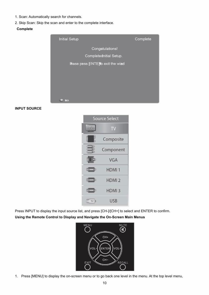
1. Scan: Automatically search for channels.
2. Skip Scan: Skip the scan and enter to the complete interface.
Complete
INPUT SOURCE
Press INPUT to display the input source list, and press [CH-]/[CH+] to select and ENTER to confirm.
Using the Remote Control to Display and Navigate the On-Screen Main Menus
1. Press [MENU] to display the on-screen menu or to go back one level in the menu. At the top level menu,
11
pressing the MENU button will exit the menu.
2. Use the [VOL-] or [VOL+] buttons to highlight the desired menu icon.Press [ENTER] to select it.
3. Use the [CH+] or [CH-] buttons to scroll up and down through the features.
4. Follow the instructions on thescreen.
5. Press [EXIT] to immediately exit the menu. Press once to display the on-screen menu, and press again to return
to normal view. If no buttons are pressed, the menu closes automatically after about 60 seconds.
To exit the menus:Press [EXIT] (or [MENU])
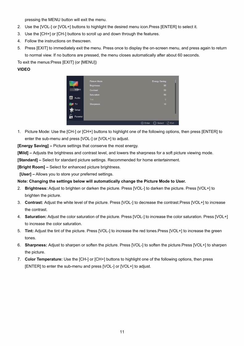
VIDEO
1. Picture Mode: Use the [CH-] or [CH+] buttons to highlight one of the following options, then press [ENTER] to
enter the sub-menu and press [VOL-] or [VOL+] to adjust.
[Energy Saving] – Picture settings that conserve the most energy.
[Mild] – Adjusts the brightness and contrast level, and lowers the sharpness for a soft picture viewing mode.
[Standard] – Select for standard picture settings. Recommended for home entertainment.
[Bright Room] – Select for enhanced picture brightness.
[User] – Allows you to store your preferred settings.
Note: Changing the settings below will automatically change the Picture Mode to User. 2. Brightness: Adjust to brighten or darken the picture. Press [VOL-] to darken the picture. Press [VOL+] to
brighten the picture.
3. Contrast: Adjust the white level of the picture. Press [VOL-] to decrease the contrast.Press [VOL+] to increase
the contrast.
4. Saturation: Adjust the color saturation of the picture. Press [VOL-] to increase the color saturation. Press [VOL+]
to increase the color saturation.
5. Tint: Adjust the tint of the picture. Press [VOL-] to increase the red tones.Press [VOL+] to increase the green
tones.
6. Sharpness: Adjust to sharpen or soften the picture. Press [VOL-] to soften the picture.Press [VOL+] to sharpen
the picture.
7. Color Temperature: Use the [CH-] or [CH+] buttons to highlight one of the following options, then press
[ENTER] to enter the sub-menu and press [VOL-] or [VOL+] to adjust.
12
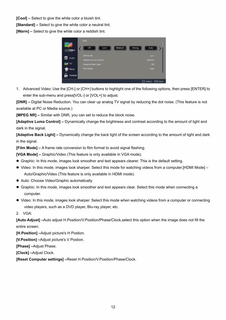
[Cool] – Select to give the white color a bluish tint.
[Standard] – Select to give the white color a neutral tint.
[Warm] – Select to give the white color a reddish tint.
1. Advanced Video: Use the [CH-] or [CH+] buttons to highlight one of the following options, then press [ENTER] to
enter the sub-menu and press[VOL-] or [VOL+] to adjust.
[DNR] – Digital Noise Reduction. You can clear up analog TV signal by reducing the dot noise. (This feature is not
available at PC or Media source.)
[MPEG NR] – Similar with DNR, you can set to reduce the block noise.
[Adaptive Luma Control] – Dynamically change the brightness and contrast according to the amount of light and
dark in the signal.
[Adaptive Back Light] – Dynamically change the back light of the screen according to the amount of light and dark
in the signal.
[Film Mode] – A frame rate conversion to film format to avoid signal flashing.
[VGA Mode] – Graphic/Video (This feature is only available in VGA mode).
� Graphic: In this mode, images look smoother and text appears clearer. This is the default setting.
� Video: In this mode, images look sharper. Select this mode for watching videos from a computer.[HDMI Mode] –
Auto/Graphic/Video (This feature is only available in HDMI mode).
� Auto: Choose Video/Graphic automatically.
� Graphic: In this mode, images look smoother and text appears clear. Select this mode when connecting a
computer.
� Video: In this mode, images look sharper. Select this mode when watching videos from a computer or connecting
video players, such as a DVD player, Blu-ray player, etc.
2. VGA:
[Auto Adjust] –Auto adjust H.Position/V.Position/Phase/Clock,select this option when the image does not fill the
entire screen.
[H.Position] –Adjust picture's H Postion.
[V.Position] –Adjust picture's V Postion.
[Phase] –Adjust Phase.
[Clock] –Adjust Clock.
[Reset Computer settings] –Reset H.Position/V.Position/Phase/Clock.
13
AUDIO
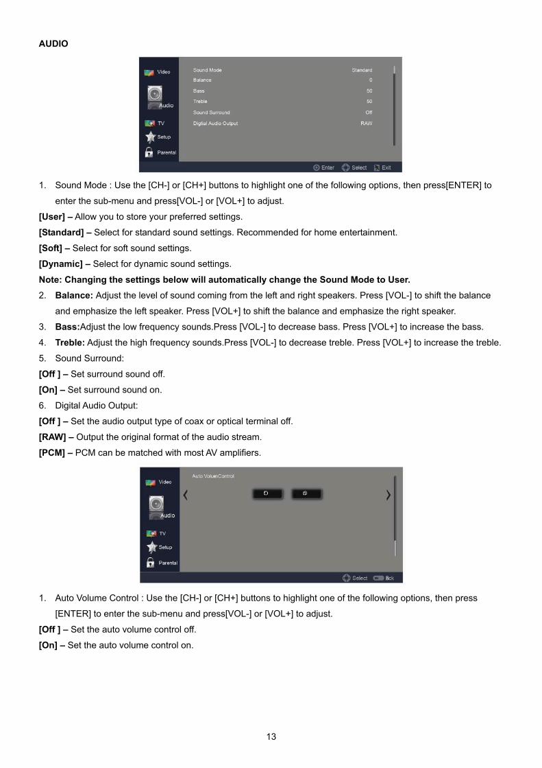
1. Sound Mode : Use the [CH-] or [CH+] buttons to highlight one of the following options, then press[ENTER] to
enter the sub-menu and press[VOL-] or [VOL+] to adjust.
[User] – Allow you to store your preferred settings.
[Standard] – Select for standard sound settings. Recommended for home entertainment.
[Soft] – Select for soft sound settings.
[Dynamic] – Select for dynamic sound settings.
Note: Changing the settings below will automatically change the Sound Mode to User. 2. Balance: Adjust the level of sound coming from the left and right speakers. Press [VOL-] to shift the balance
and emphasize the left speaker. Press [VOL+] to shift the balance and emphasize the right speaker.
3. Bass:Adjust the low frequency sounds.Press [VOL-] to decrease bass. Press [VOL+] to increase the bass.
4. Treble: Adjust the high frequency sounds.Press [VOL-] to decrease treble. Press [VOL+] to increase the treble.
5. Sound Surround:
[Off ] – Set surround sound off.
[On] – Set surround sound on.
6. Digital Audio Output:
[Off ] – Set the audio output type of coax or optical terminal off.
[RAW] – Output the original format of the audio stream.
[PCM] – PCM can be matched with most AV amplifiers.
1. Auto Volume Control : Use the [CH-] or [CH+] buttons to highlight one of the following options, then press
[ENTER] to enter the sub-menu and press[VOL-] or [VOL+] to adjust.
[Off ] – Set the auto volume control off.
[On] – Set the auto volume control on.

14
TV
1. Signal Type : Use the [CH-] or [CH+] buttons to highlight one of the following options, then press [ENTER] to
enter the sub-menu and press[VOL-] or [VOL+] to adjust.
[Antenna] – Set the signal type to antenna. When set to Air, the TV can receive analog and digital (ATSC)
broadcasting signal.
[Cable] – Set the signal type to cable. When set to Cable, the TV can receive analog and QAM broadcasting signal.
2. Auto Channel Search: Highlight and press ENTER to start the channel scan.
3. Channel Skip: Manually add and skip channels in your program list.
4. Favorite List: Manually add and skip channels in your favorite list.
SETUP
1. Menu Language : Use the [CH-] or [CH+] buttons to highlight one of the following options, then press [ENTER]
to enter the sub-menu and press[VOL-] or [VOL+] to adjust.
Set the On-Screen-Display language.English/Espanol/Francais.
2. Aspect Ratio: Press to switch the display mode: Normal, Wide, Cinema, Zoom when having signal.
3. MTS: Set the preferred sound track of analog channels. Mono/Stereo/SAP.
4. No Signal Power Off: When this option is set to On, the TV will automatically turn off when there is no input
signal.
5. Blue Screen: When this option is set to On, the screen will be blue instead of black when there is no input
signal.
6. Audio Only: Press [ENTER] to turn down backlight ,and press any key to resume.
7. Time Setup: Set Time Zone/Time/Sleep Timer/Auto Sleep.
8. Caption: Set Caption Display/Analog Closed Caption/Digital Closed Caption /Digital Caption Style. For details,
please refer to page 22.
9. All Reset: Reset all the Settings to default.
15
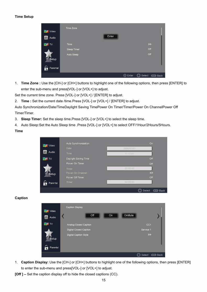
Time Setup
1. Time Zone : Use the [CH-] or [CH+] buttons to highlight one of the following options, then press [ENTER] to
enter the sub-menu and press[VOL-] or [VOL+] to adjust.
Set the current time zone. Press [VOL-] or [VOL+] / [ENTER] to adjust.
2. Time : Set the current date /time.Press [VOL-] or [VOL+] / [ENTER] to adjust.
Auto Synchronization/Date/TimeDaylight Saving TimePower On Timer/Timer/Power On ChannelPower Off
Timer/Timer.
3. Sleep Timer: Set the sleep time.Press [VOL-] or [VOL+] to select the sleep time.
4. Auto Sleep:Set the Auto Sleep time .Press [VOL-] or [VOL+] to select OFF/1Hour/2Hours/5Hours.
Time
Caption
1. Caption Display: Use the [CH-] or [CH+] buttons to highlight one of the following options, then press [ENTER]
to enter the sub-menu and press[VOL-] or [VOL+] to adjust.
[Off ] – Set the caption display off to hide the closed captions (CC).
16
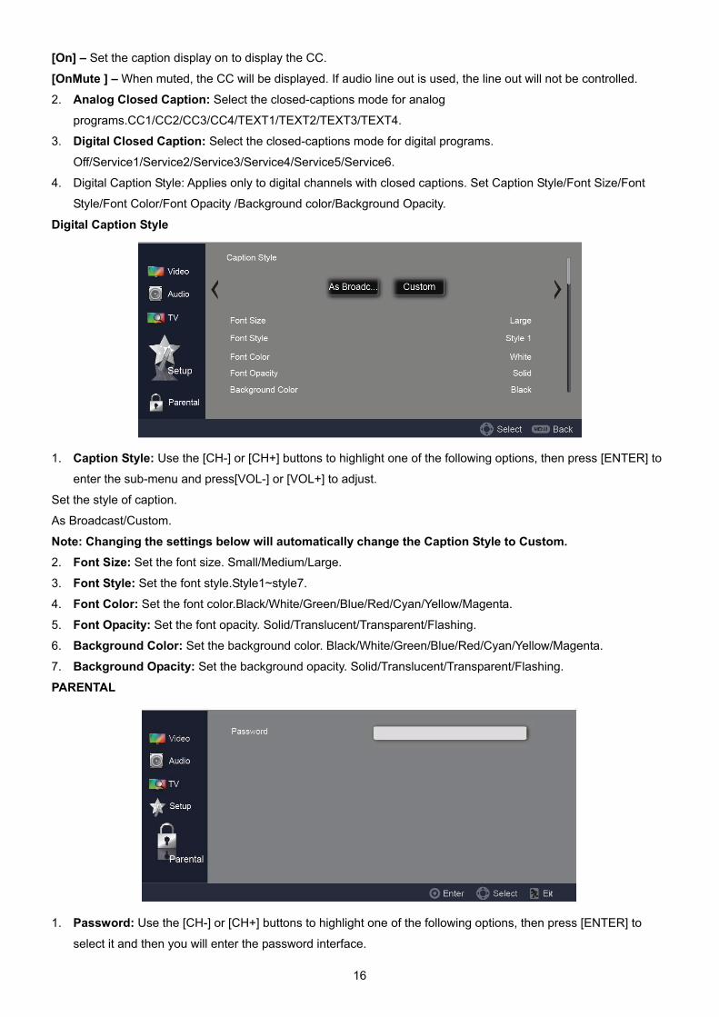
[On] – Set the caption display on to display the CC.
[OnMute ] – When muted, the CC will be displayed. If audio line out is used, the line out will not be controlled.
2. Analog Closed Caption: Select the closed-captions mode for analog
programs.CC1/CC2/CC3/CC4/TEXT1/TEXT2/TEXT3/TEXT4.
3. Digital Closed Caption: Select the closed-captions mode for digital programs.
Off/Service1/Service2/Service3/Service4/Service5/Service6.
4. Digital Caption Style: Applies only to digital channels with closed captions. Set Caption Style/Font Size/Font
Style/Font Color/Font Opacity /Background color/Background Opacity.
Digital Caption Style
1. Caption Style: Use the [CH-] or [CH+] buttons to highlight one of the following options, then press [ENTER] to
enter the sub-menu and press[VOL-] or [VOL+] to adjust.
Set the style of caption.
As Broadcast/Custom.
Note: Changing the settings below will automatically change the Caption Style to Custom. 2. Font Size: Set the font size. Small/Medium/Large.
3. Font Style: Set the font style.Style1~style7.
4. Font Color: Set the font color.Black/White/Green/Blue/Red/Cyan/Yellow/Magenta.
5. Font Opacity: Set the font opacity. Solid/Translucent/Transparent/Flashing.
6. Background Color: Set the background color. Black/White/Green/Blue/Red/Cyan/Yellow/Magenta.
7. Background Opacity: Set the background opacity. Solid/Translucent/Transparent/Flashing.
PARENTAL
1. Password: Use the [CH-] or [CH+] buttons to highlight one of the following options, then press [ENTER] to
select it and then you will enter the password interface.

17
After entering the correct password, you will see the submenu shown below. The default password is “0000”.
1. System Block: Use the [CH-] or [CH+] buttons to highlight one of the following options, then press [ENTER] to
enter the sub-menu and press[VOL-] or [VOL+] to adjust.
Set the channel / program block on or off.
2. Channel Block: Set the channels to be blocked.
3. Program Block: Use the [CH-] or [CH+] buttons to highlight one of the following options, then press [ENTER] to
enter the sub-menu and press[VOL-] or [VOL+] to adjust.
Set the program to be locked. For details please refer to pages 24~25.
[Rating Enable] – Set the ratings on or off.
[U.S. TV Ratings] – See page 24.
18
[U.S. Movie Rating]–See page 24.
[Canadian English Ratings] – See page 24.
[Canadian French Ratings] – See page 25.
[Open V-chip] – Set the V-chip on.
[Clear Open V-chip Data] – Set the V-chip data to default values.
[Block Unrated] – Block the programs that do not have any valid rating flag.
4. Change Password: Enter the 4-digital new password and confirm it. New Password/Confirm password.
5. Clean All: Set the items in the lock menu to default values.
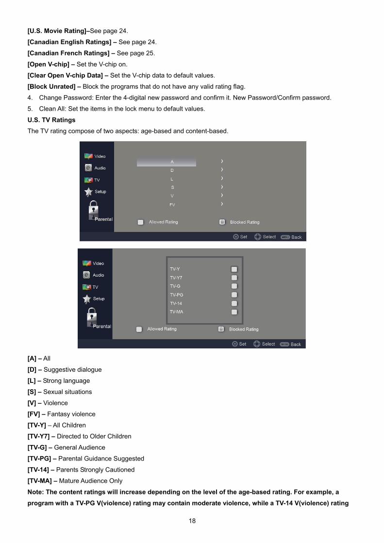
U.S. TV Ratings The TV rating compose of two aspects: age-based and content-based.
[A] – All
[D] – Suggestive dialogue
[L] – Strong language
[S] – Sexual situations
[V] – Violence
[FV] – Fantasy violence
[TV-Y] – All Children
[TV-Y7] – Directed to Older Children
[TV-G] – General Audience
[TV-PG] – Parental Guidance Suggested
[TV-14] – Parents Strongly Cautioned
[TV-MA] – Mature Audience Only
Note: The content ratings will increase depending on the level of the age-based rating. For example, a program with a TV-PG V(violence) rating may contain moderate violence, while a TV-14 V(violence) rating

19
may contain intense violence. So locking a higher level option will automatically cause locking the options that has more sensitive level. U.S. Movie Ratings This system defines the rating control which come from MPAA rules.
[G] – General audience. All ages admitted.
[PG] – Parental guidance suggested.Some material may not be suitable for children.
[PG-13] – Parents strongly cautioned. Some material may be inappropriate for children under 13.
[R] – Restricted. Children under 17 require accompanying parent or adult guardian.
[NC-17] – No one 17 and under admitted.
[X] – Adult audience only.
Canadian English Rating These ratings are for programs which are using English rating system.
[C] – Children
[C8+] – Children 8 years and older
[G] – General programming
[PG] – Parental guidance
[14+] – Viewers 14 and older
[18+] – Adult programming
20
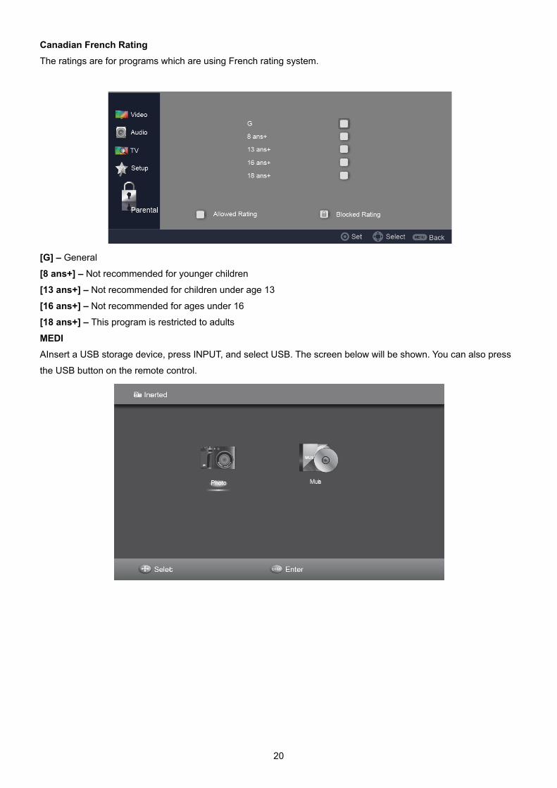
Canadian French Rating The ratings are for programs which are using French rating system.
[G] – General
[8 ans+] – Not recommended for younger children
[13 ans+] – Not recommended for children under age 13
[16 ans+] – Not recommended for ages under 16
[18 ans+] – This program is restricted to adults
MEDI AInsert a USB storage device, press INPUT, and select USB. The screen below will be shown. You can also press
the USB button on the remote control.
21
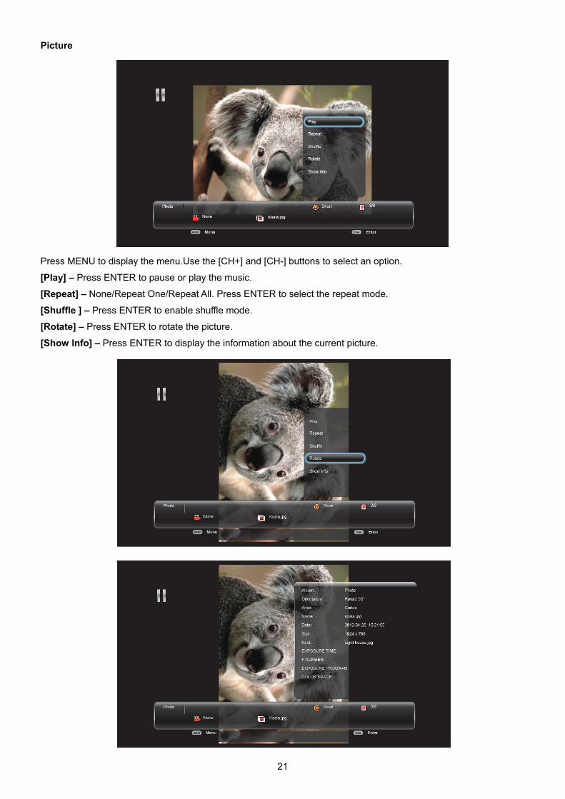
Picture
Press MENU to display the menu.Use the [CH+] and [CH-] buttons to select an option.
[Play] – Press ENTER to pause or play the music.
[Repeat] – None/Repeat One/Repeat All. Press ENTER to select the repeat mode.
[Shuffle ] – Press ENTER to enable shuffle mode.
[Rotate] – Press ENTER to rotate the picture.
[Show Info] – Press ENTER to display the information about the current picture.
22
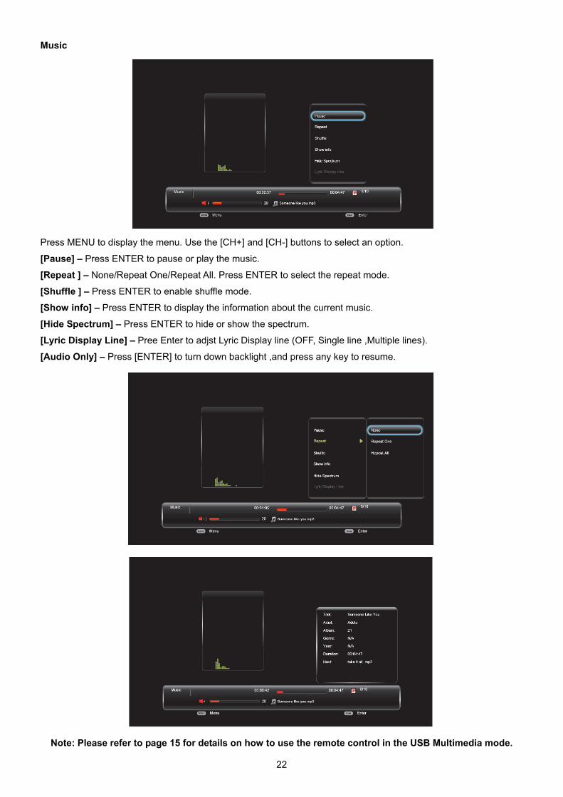
Music
Press MENU to display the menu. Use the [CH+] and [CH-] buttons to select an option.
[Pause] – Press ENTER to pause or play the music.
[Repeat ] – None/Repeat One/Repeat All. Press ENTER to select the repeat mode.
[Shuffle ] – Press ENTER to enable shuffle mode.
[Show info] – Press ENTER to display the information about the current music.
[Hide Spectrum] – Press ENTER to hide or show the spectrum.
[Lyric Display Line] – Pree Enter to adjst Lyric Display line (OFF, Single line ,Multiple lines).
[Audio Only] – Press [ENTER] to turn down backlight ,and press any key to resume.
Note: Please refer to page 15 for details on how to use the remote control in the USB Multimedia mode.
23
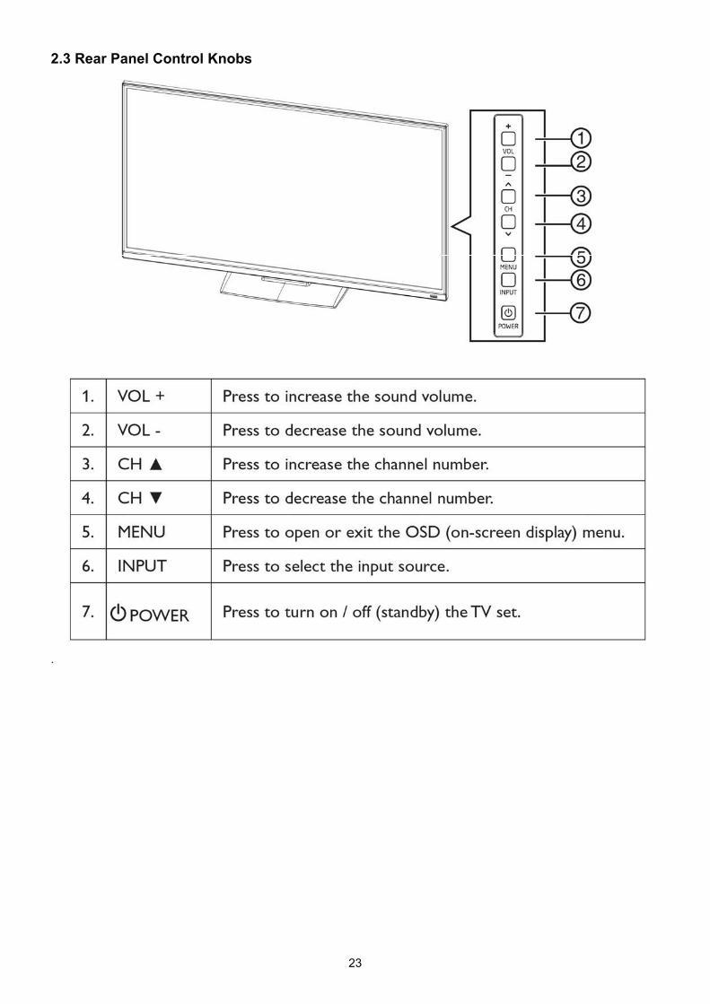
2.3 Rear Panel Control Knobs
.
24
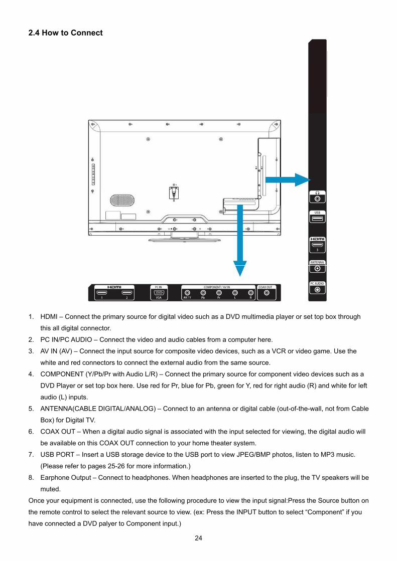
2.4 How to Connect
1. HDMI – Connect the primary source for digital video such as a DVD multimedia player or set top box through
this all digital connector.
2. PC IN/PC AUDIO – Connect the video and audio cables from a computer here.
3. AV IN (AV) – Connect the input source for composite video devices, such as a VCR or video game. Use the
white and red connectors to connect the external audio from the same source.
4. COMPONENT (Y/Pb/Pr with Audio L/R) – Connect the primary source for component video devices such as a
DVD Player or set top box here. Use red for Pr, blue for Pb, green for Y, red for right audio (R) and white for left
audio (L) inputs.
5. ANTENNA(CABLE DIGITAL/ANALOG) – Connect to an antenna or digital cable (out-of-the-wall, not from Cable
Box) for Digital TV.
6. COAX OUT – When a digital audio signal is associated with the input selected for viewing, the digital audio will
be available on this COAX OUT connection to your home theater system.
7. USB PORT – Insert a USB storage device to the USB port to view JPEG/BMP photos, listen to MP3 music.
(Please refer to pages 25-26 for more information.)
8. Earphone Output – Connect to headphones. When headphones are inserted to the plug, the TV speakers will be
muted.
Once your equipment is connected, use the following procedure to view the input signal:Press the Source button on
the remote control to select the relevant source to view. (ex: Press the INPUT button to select “Component” if you
have connected a DVD palyer to Component input.)
25
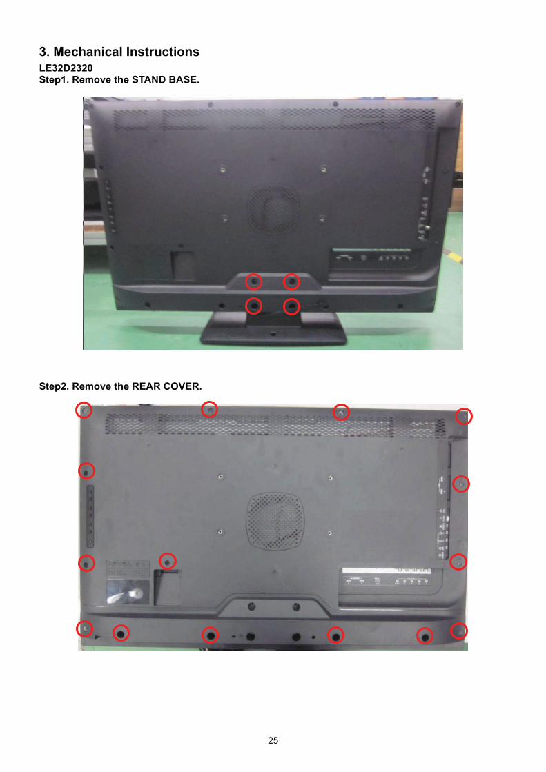
3. Mechanical Instructions LE32D2320 Step1. Remove the STAND BASE.
Step2. Remove the REAR COVER.
26
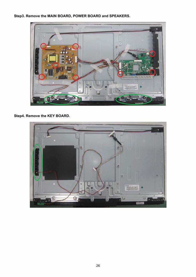
Step3. Remove the MAIN BOARD, POWER BOARD and SPEAKERS.
Step4. Remove the KEY BOARD.
27
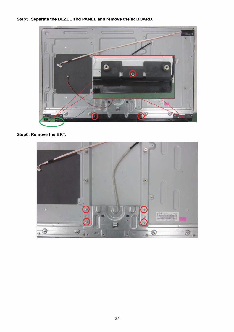
Step5. Separate the BEZEL and PANEL and remove the IR BOARD.
Step6. Remove the BKT.

28
LE39D2380 Step1. Remove the STAND BASE.
Step2. Remove the REAR COVER.
29
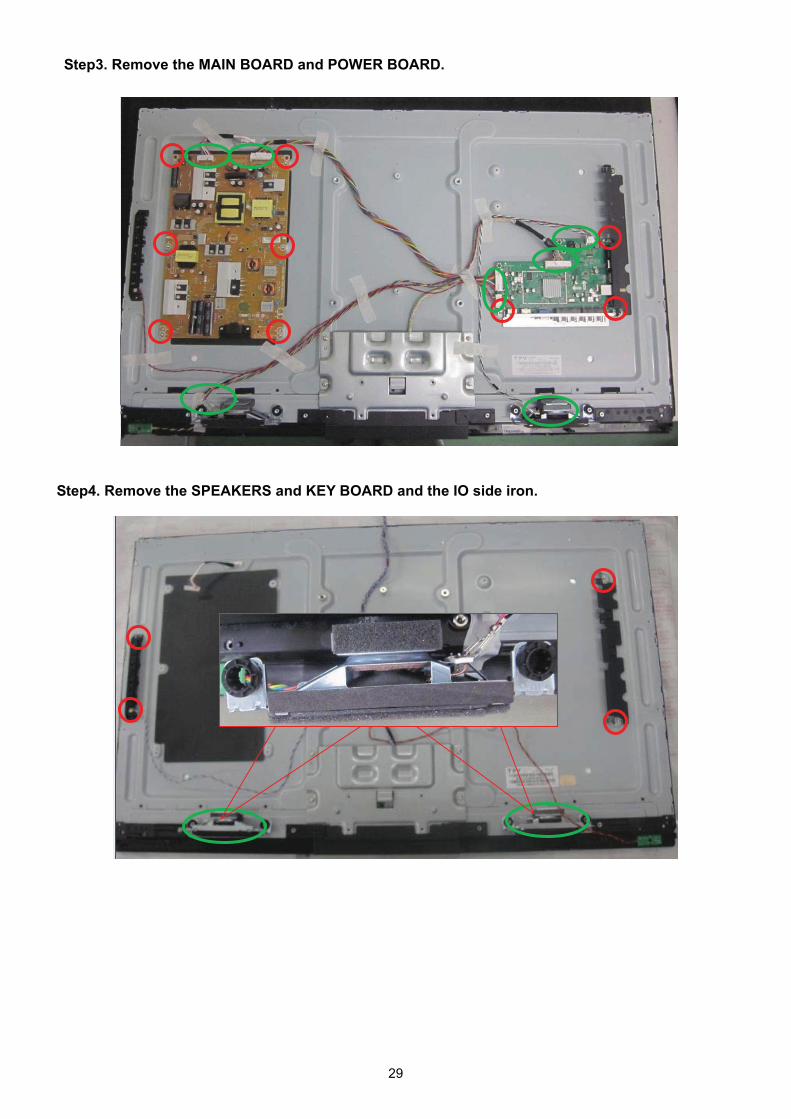
Step3. Remove the MAIN BOARD and POWER BOARD.
Step4. Remove the SPEAKERS and KEY BOARD and the IO side iron.
30
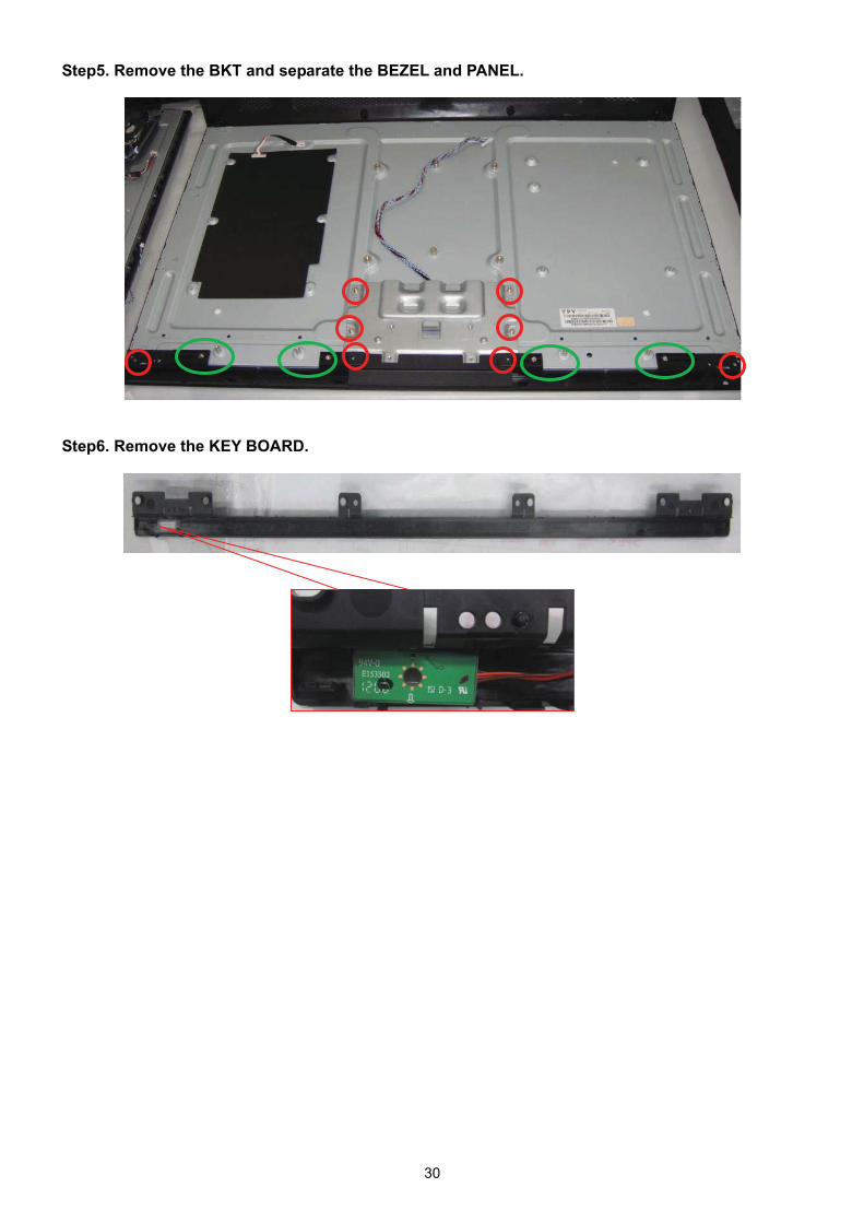
Step5. Remove the BKT and separate the BEZEL and PANEL.
Step6. Remove the KEY BOARD.

31
LE42D2380 Step1. Remove the STAND BASE.
Step2. Remove the REAR COVER.
32
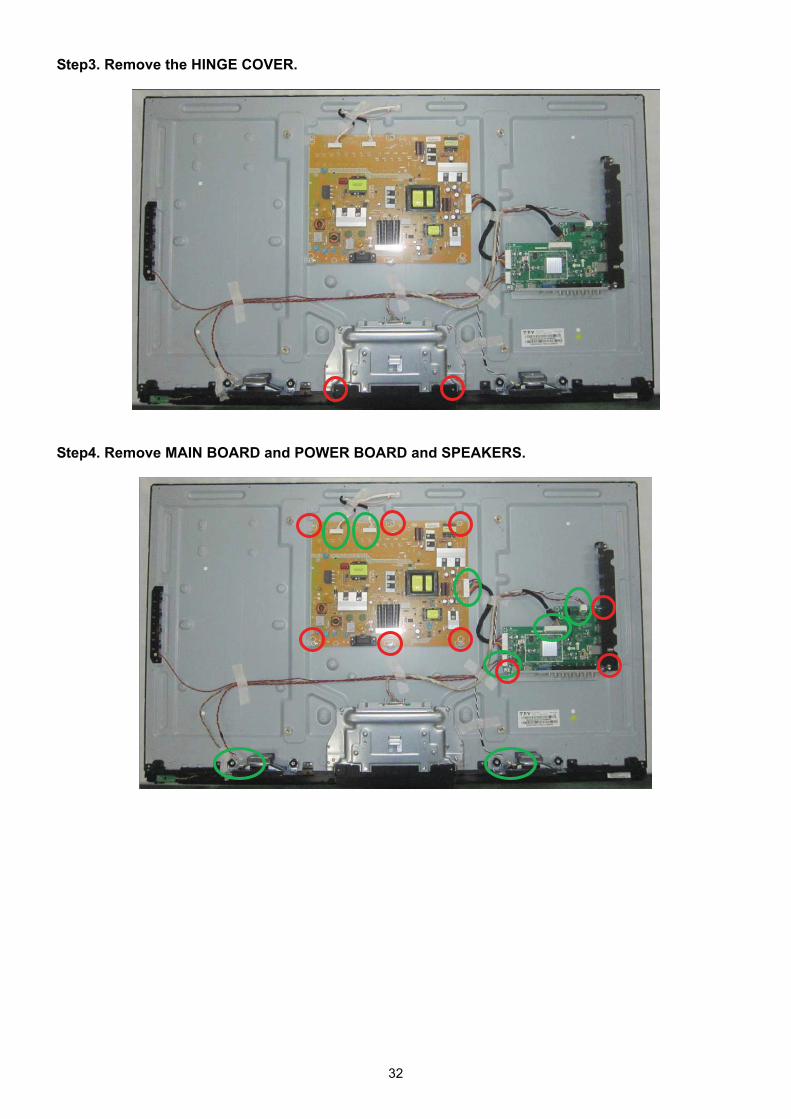
Step3. Remove the HINGE COVER.
Step4. Remove MAIN BOARD and POWER BOARD and SPEAKERS.

33
Step5. Remove the SPEAKERS and KEY BOARD and the IO side iron.
Step6. Remove the BKT and separate the BEZEL and PANEL.
Step7.Remove the IR BOARD

34
LE46D2380 Step1. Remove the STAND BASE.
Step2. Remove the REAR COVER.
35
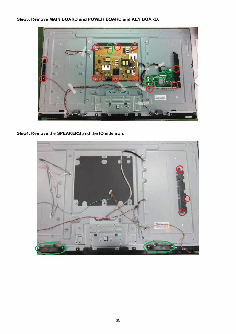
Step3. Remove MAIN BOARD and POWER BOARD and KEY BOARD.
Step4. Remove the SPEAKERS and the IO side iron.
36
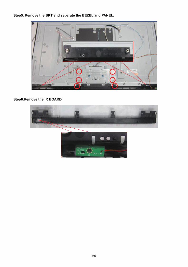
Step5. Remove the BKT and separate the BEZEL and PANEL.
Step6.Remove the IR BOARD
37
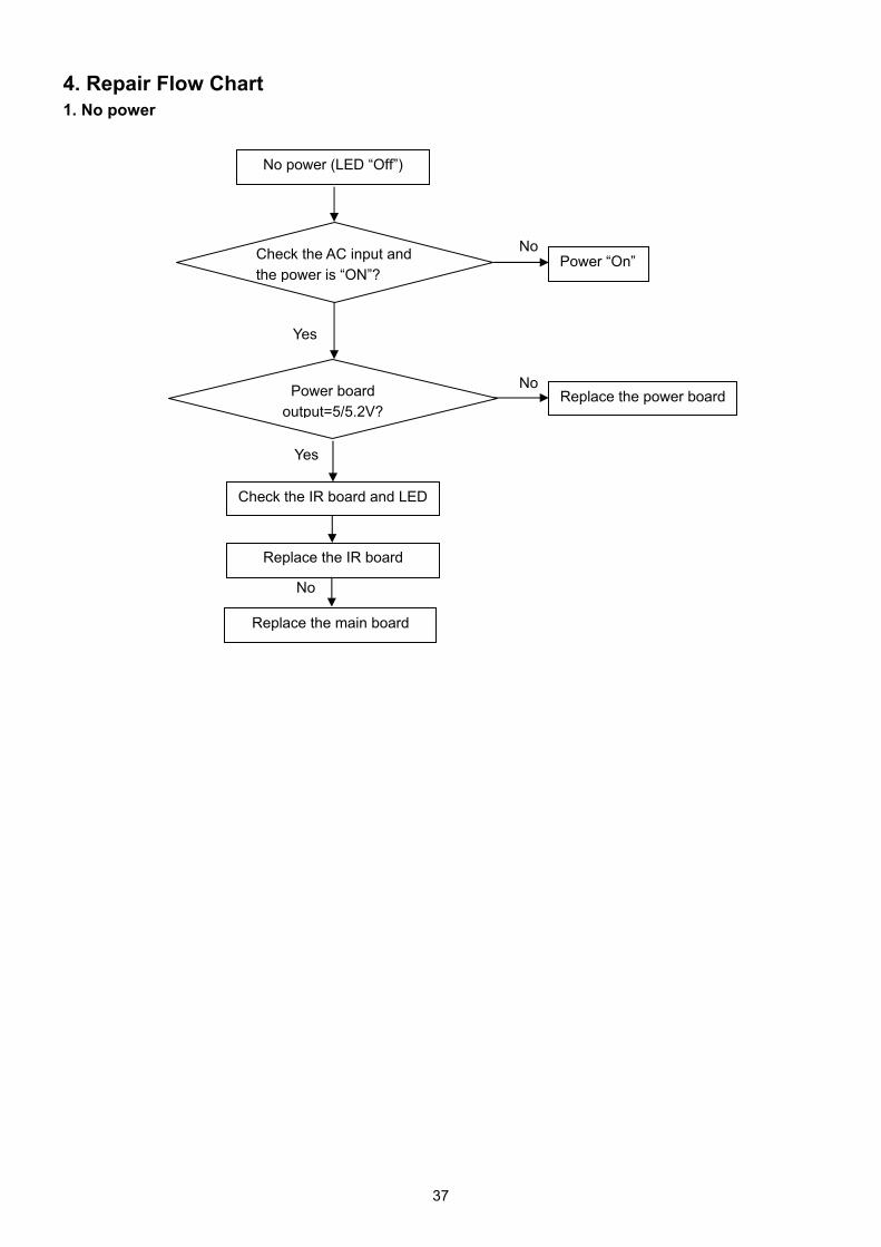
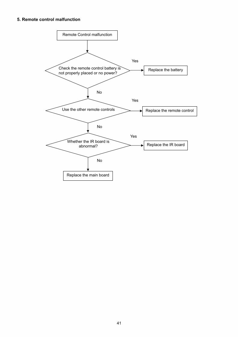
4. Repair Flow Chart 1. No power
No power (LED “Off”)
Check the AC input and the power is “ON”?
Power “On”
Check the IR board and LED
Replace the IR board
Replace the main board
Power board output=5/5.2V?
Replace the power board
No
Yes
No
Yes
No

38
2. Can’t start
Can’t start LED red
Replace the main board
Replace the Power board
No
Yes
No
Yes
No
No
Power board output 24V?
Check the power key is under control?
Check the IR receiver is normal?
Replace the power board
Replace the key board
Yes
Replace the IR board
39
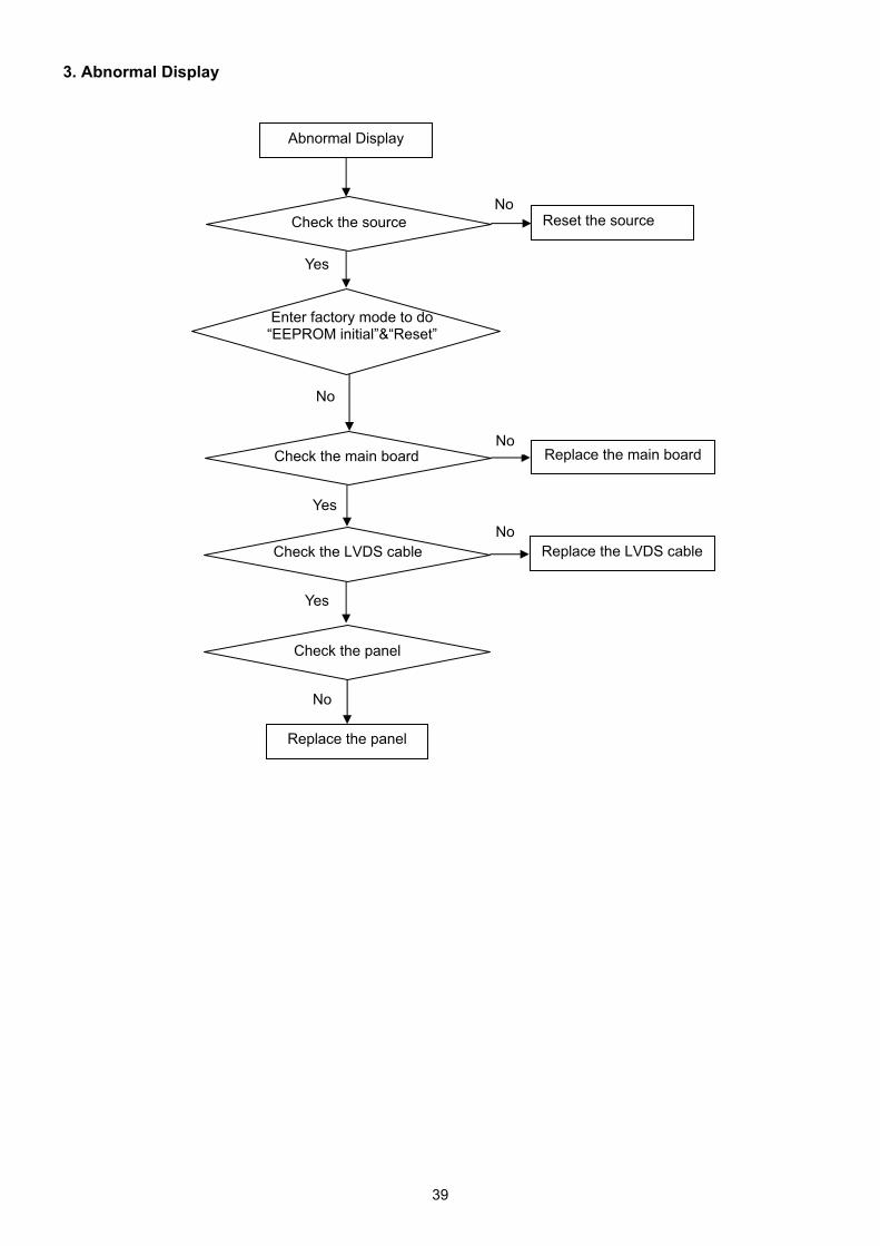
3. Abnormal Display
Abnormal Display
Reset the source Check the source
Check the panel
Replace the main board
Replace the LVDS cable
Replace the panel
No
No
No
Yes
Yes
Yes
No
No
Check the main board
Enter factory mode to do “EEPROM initial”&“Reset”
Check the LVDS cable
40
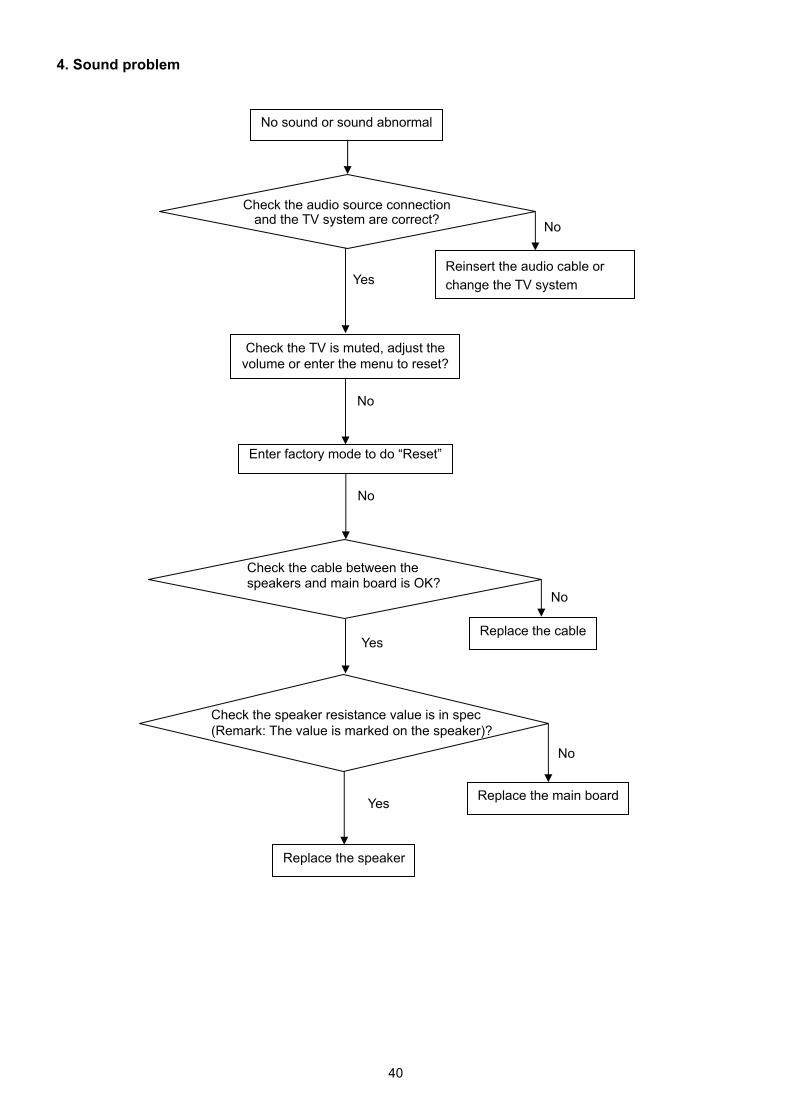
4. Sound problem
No
Check the cable between the speakers and main board is OK?
No sound or sound abnormal
Check the TV is muted, adjust the volume or enter the menu to reset?
Reinsert the audio cable or change the TV system
Replace the cable
Replace the speaker
Replace the main board
No
Yes
Check the speaker resistance value is in spec (Remark: The value is marked on the speaker)?
Check the audio source connection and the TV system are correct?
Yes
No
Yes
No
Enter factory mode to do “Reset”
No
41
5. Remote control malfunction
Remote Control malfunction
Replace the battery
Replace the remote control
Whether the IR board is abnormal?
Yes
No
Replace the IR board
Replace the main board
No
Yes
No
Yes
Use the other remote controls
Check the remote control battery is not properly placed or no power?
42
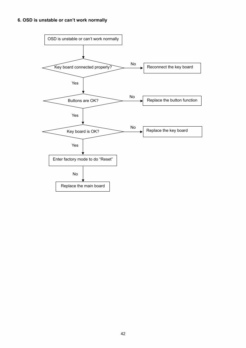
6. OSD is unstable or can’t work normally
Key board connected properly? Reconnect the key board
Buttons are OK? Replace the button function
Yes
No
Key board is OK? Replace the key board
Replace the main board
No
Yes
No
No
OSD is unstable or can’t work normally
Enter factory mode to do “Reset”
Yes
43
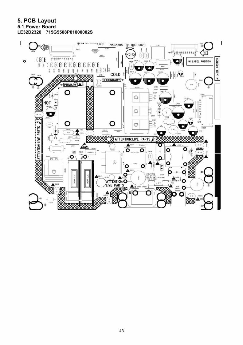
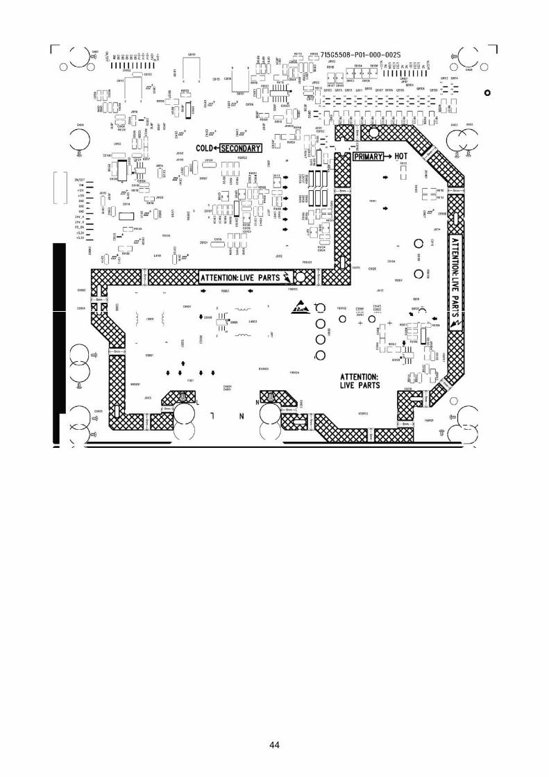
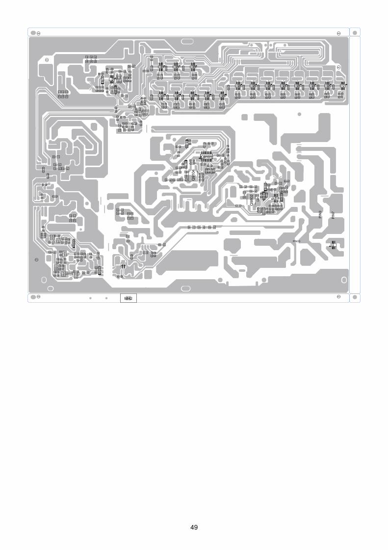
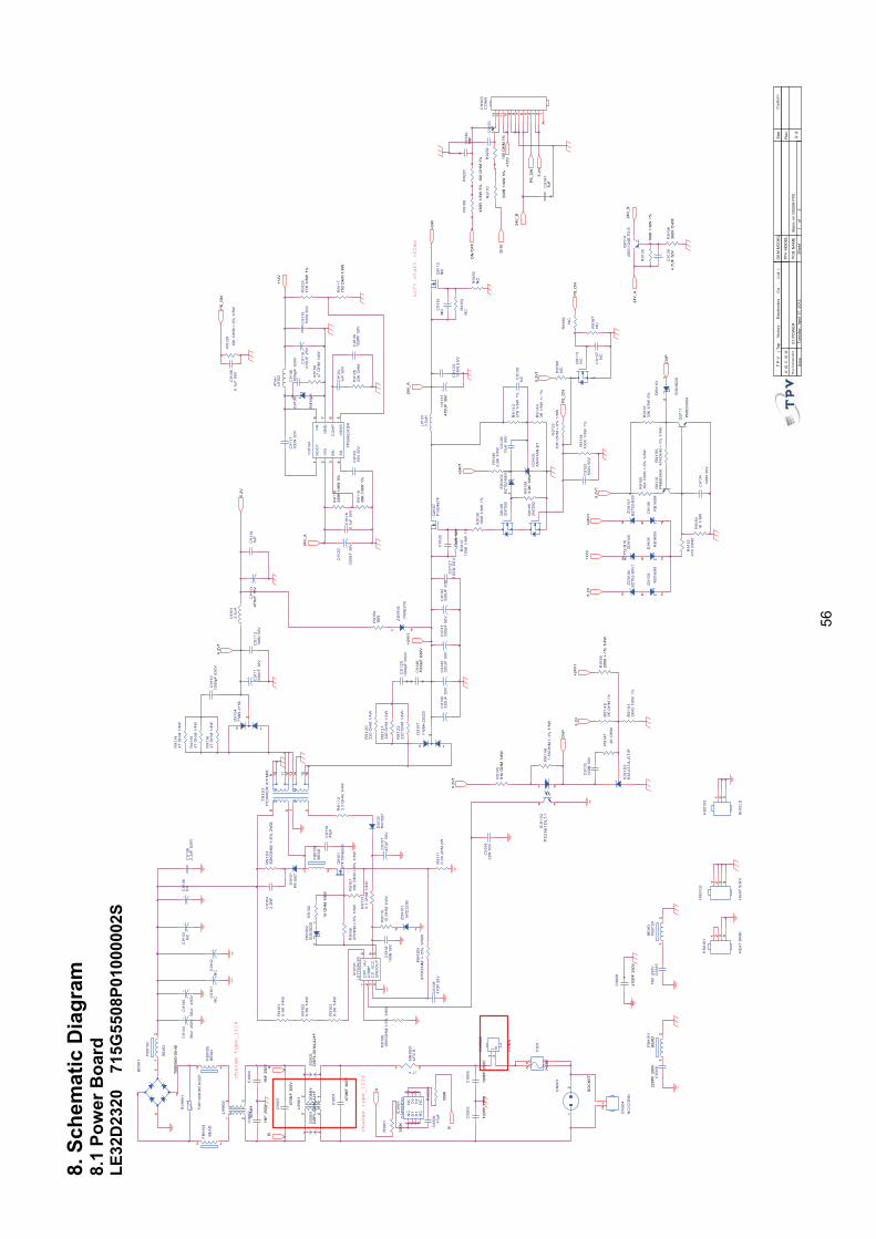
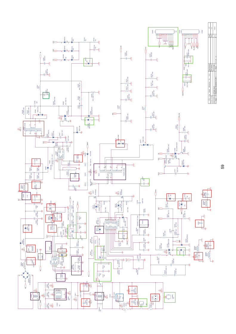
5. PCB Layout 5.1 Power Board LE32D2320 715G5508P01000002S
44
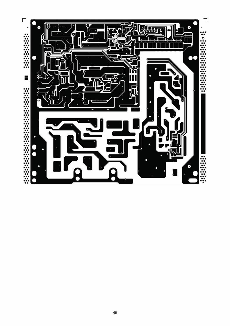
45
46
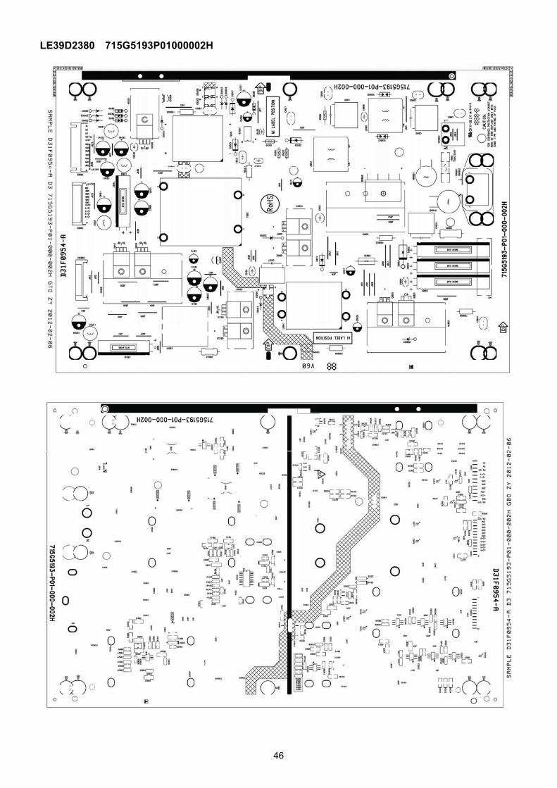
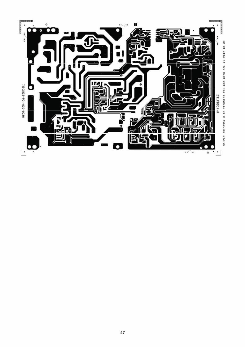
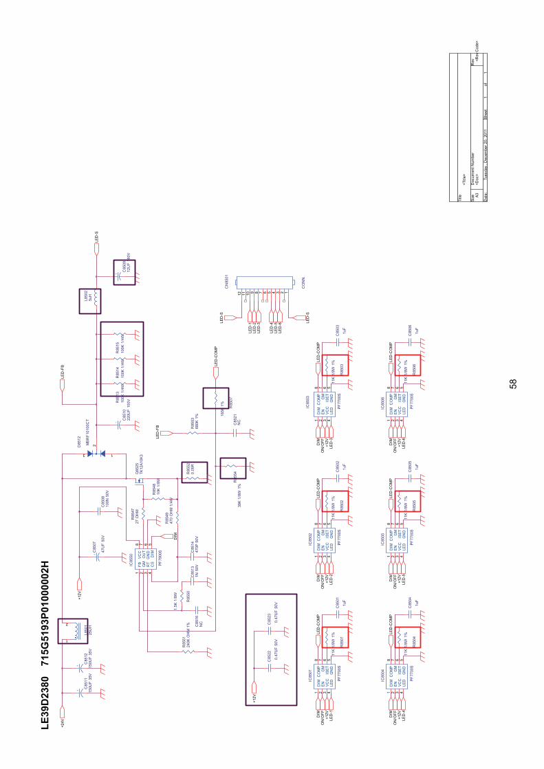
LE39D2380 715G5193P01000002H
47
48
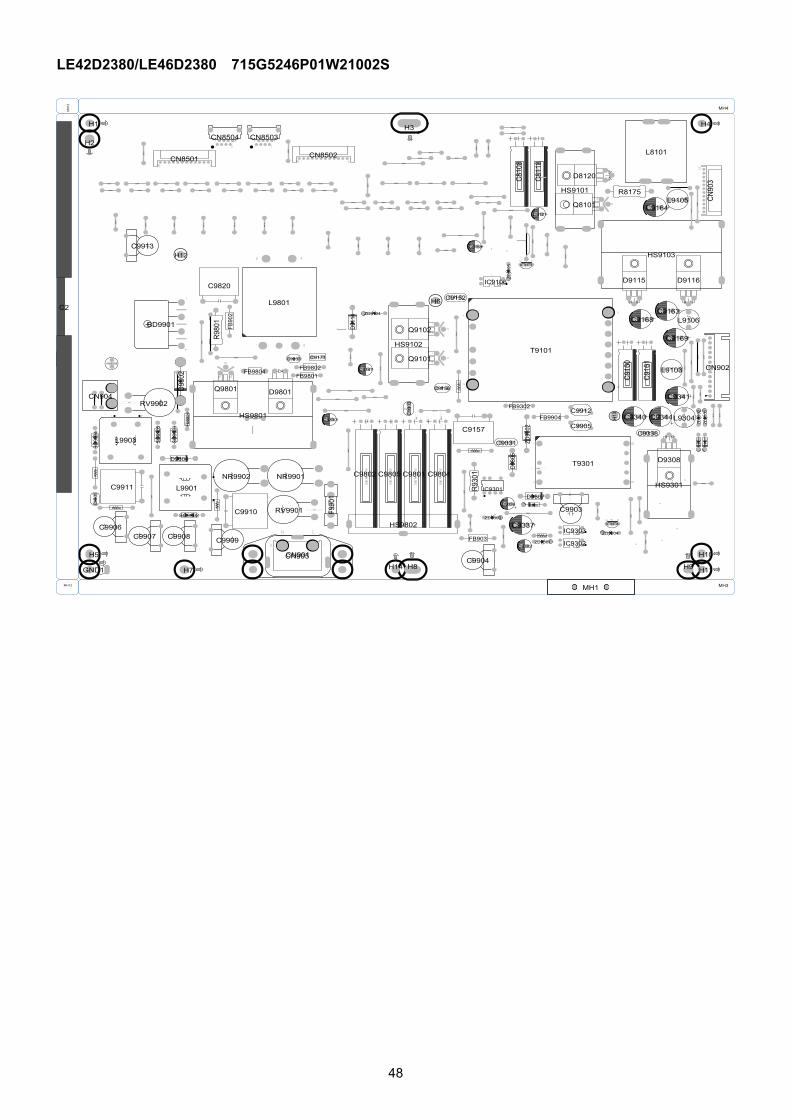
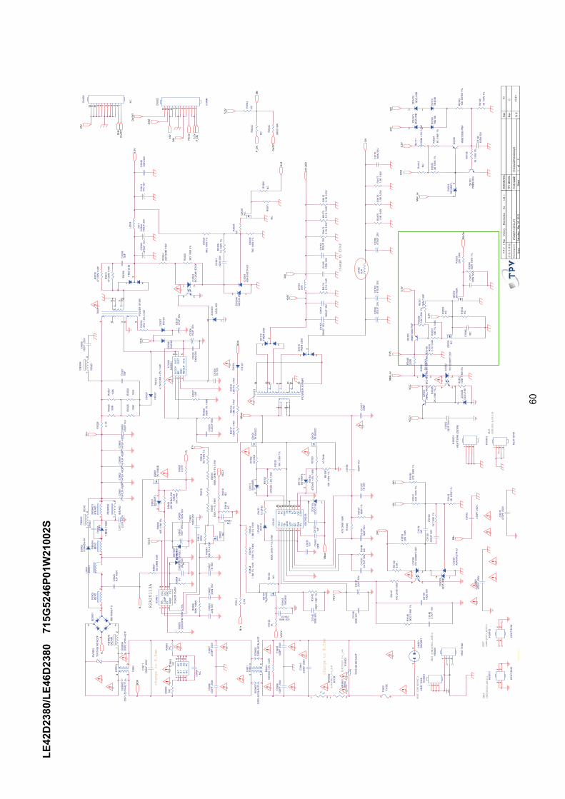
LE42D2380/LE46D2380 715G5246P01W21002S
C9147
C9156
C9302
C980
3
D910
9
D911
0
D930
5D9306
D9307
D980
2
IC9302
IC9106
IC9107
IC9303IC9304
J990
1
J930
6
J9905
J990
7
J9302
J8501 J8504 J8507 J8510 J8514 J8517
J8525
J8524
J8529
J8528
J851
3
J850
3
J850
6
J850
9
J851
2
J851
6
J851
9
J852
3
J852
6
J853
0
J854
9
J855
0
J8533
J8538J8537
J8532
J8546
J8547
J853
5
J856
4
J8548
J9906
J990
2
J9903
J9904
J8544
J8545J8543J8541
J8542
J8521
J8522J8518J8515J8511J8508J8505J8502
C8121
C9336
C9830
R930
1J9
307
H12
J8536
J911
4
J9115
J9113
J911
0
J911
1
J910
3
J910
5
J911
2
J910
9
J856
1
J8531
J8540
J910
6
J8520
J910
8
J8539
J855
8
J855
2
J852
7J9309
J930
5
J930
8
J9908
J990
9
J991
0
J911
7
J911
6
J910
7
J910
4
J855
4
J855
3
J910
2
J910
1
J930
4
J8534
J930
1
C8158J8565
J9118
H13
C9905
C9912
J991
2
J991
1
J930
3
H6
T9101
J8551
T9301
MH3
MH4
MH12
MH1
3
PIN5PIN6
DR4
DR5
DR6
DRL1
DR1
PIN4
DR2
BD1
Q1
Q2
PIN8
C990
1
D9801
F990
1
FB90
2
FB903
FB9801
IC9301
Q9801
R9904
R990
5
SG9902
SG99
03
SG99
04
SG99
05
R980
1
HS9801
C2
C9164
CN8501 CN8502
D9115 D9116
L8101
R8175
CN90
3
D8120
CN8504 CN8503
FB9802
H4H1
H5
GND1
H10
H11H9
MH1
H8
H3
HS9802
C9340
C9341
C9344
C9163C9168
C9169
C9337
H7
H2
CN902L9103
HS9103
HS9301
D911
4
FB9904
Q8101
D9308
H14
C916
0
C916
1
HS9102
HS9101
R914
1
R9329
Q9101
Q9102
C9820
ZD93
02
NR9901NR9902
R990
1
R9302
CN905
C9331C9338
L9105
L9106
L9304
C9903
C9904
C9906C9907
C9152
ZD91
01ZD
9102
ZD91
05
ZD9301
ZD9303
ZD9304
ZD9104
C810
8
C811
8C9908 C9909
D9304
C9833
FB9804
C9171
FB98
03
FB9302
CN901
CN904
C9913
C9157
C9801 C9804C9805C9802
C9910
C9911
RV9901
RV9902
L9901
L9903
BD9901
L9801
FB9805
49
C81
05
C81
06
C81
11C
8119
C9144
C9145 C9146
C91
49
C91
50
C91
51
C91
53
C91
54
C9155
C9158
C91
59
C91
65
C91
70
C93
33C9334
C93
35
C9342
C93
43
C93
01
C98
24
C9825
C98
26
C98
27
C98
28
C98
29
IC98
01
IC99
01Q91
03
Q93
01
R81
41
R81
44
R8148
R81
53
R81
54
R81
55
R81
56
R81
57
R81
61
R8162
R81
63
R91
01
R91
39
R9140
R9150 R9144
R9145
R91
46
R91
48
R9149
R9151
R91
52
R9153
R91
54
R9156
R91
58
R9159
R91
61 R9163
R91
71
R91
72
R91
73
R9174
R9175
R9176
R9177
R91
80
R9317 R9318 R9319
R93
20
R9323
R93
32
R9325
R93
26
R9327
R93
28
R93
30
R93
31
R93
34
R93
35
R93
36
R9337
R93
38
R93
39
R93
40
R93
41
R9306
R93
04
R98
04
R98
05
R98
06
R98
07
R98
10
R9813
R9815
R9816
R9342
R93
43
R93
45
C85
01
C85
02
C85
03
C85
04
C85
05
C85
06
C85
07
C85
08
C85
09
C85
10C
8511
C85
12
C85
13
C85
14
C85
15
C85
16
IC81
03
IC85
01
R85
01
R85
02
R85
03
R85
04
R85
05
R85
06
R85
07
R85
08
R85
09
R85
10R
8511
R85
12
R85
13
R85
14
R85
15
R85
16
C81
57
C85
18
C85
19
C85
20
C85
21
C85
22
C85
23
C85
24
C85
25
C85
26
C85
27
C85
28
C85
29
C85
30
C85
31
C85
32
IC85
03
IC85
05
IC85
04
IC85
07
IC85
06
IC85
08
IC85
02
IC85
12
IC85
10
IC85
09
IC85
11
IC85
13
IC85
16
IC85
14
IC85
15
C93
45
R93
09
R93
10
Q93
04
MH5
MH6
MH7
MH8
MH9 MH10
MH11
R98
17
R81
58
R9142
JR9101
R81
76
R81
47
R8145
C9346
R98
09
R91
47
R91
60
R9808
R9308
R93
11
R93
12
R9313
R93
16
R9321
R9322
R9178
Q93
05
Q93
06
Q93
08
C91
48
R9102
R91
03
C9831
R9307
JR9102
JR8101
C81
13
R93
46Q93
02
C9832
R9111
R9138
R91
43R9315
R9324
R9333
R93
44
R98
18
R9819
Q91
06
R9303
R9814
R9165
C9162
R9164
R91
55
R98
11
JR91
03
R8177
C91
66
JR9104
PIN
3
PIN
7
PIN10
D81
18
D91
12D
9113
D98
03
MH2
IC9101
ZD81
03
D93
01
D93
02
Q91
04
Q98
02
Q9303
ZD91
06
ZD91
07
50
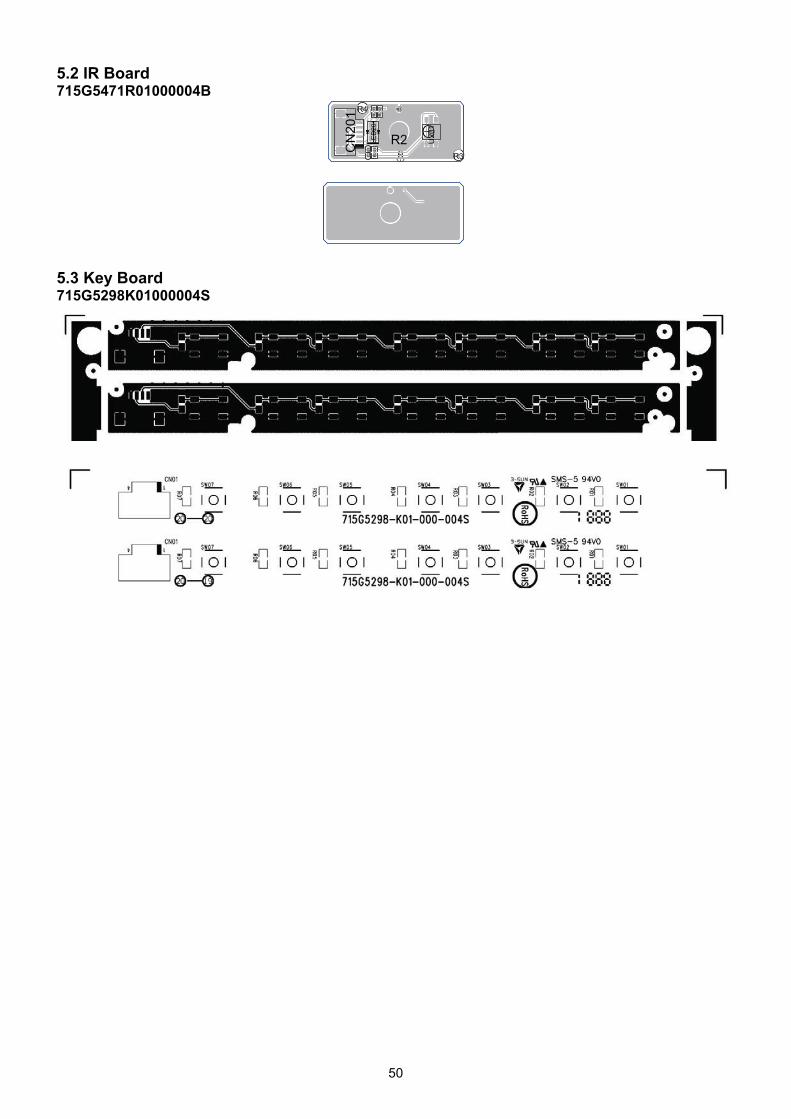
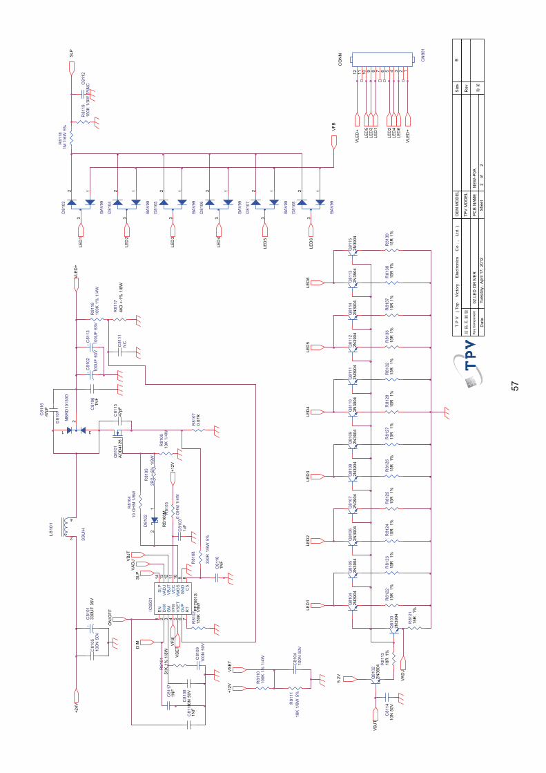
5.2 IR Board 715G5471R01000004B
C20
1R
201
R20
2R
203 R1
R2R3
R4
CN
201
LED
201
U20
1
5.3 Key Board 715G5298K01000004S
51
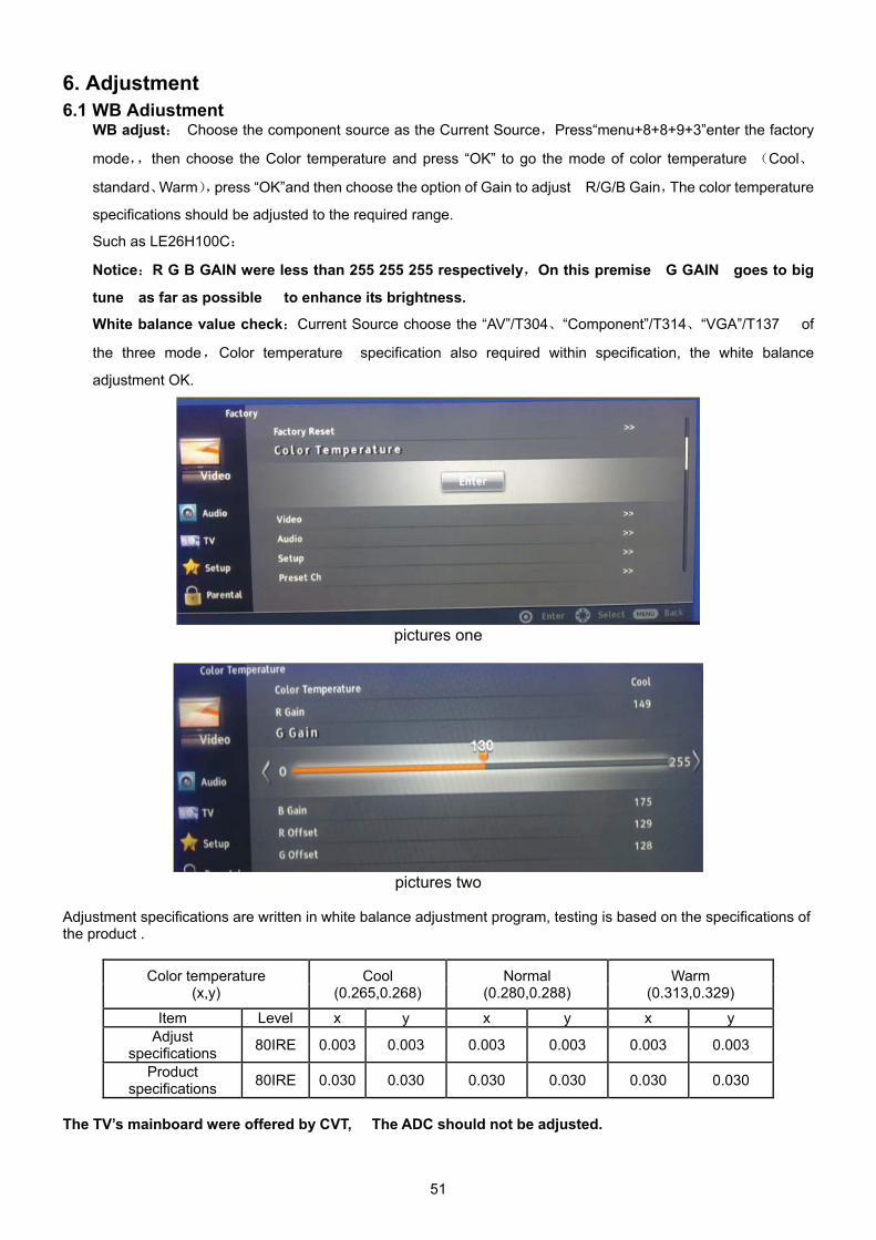
6. Adjustment 6.1 WB Adiustment
WB adjust Choose the component source as the Current Source Press“menu+8+8+9+3”enter the factory
mode then choose the Color temperature and press “OK” to go the mode of color temperature Cool
standard Warm press “OK”and then choose the option of Gain to adjust R/G/B Gain The color temperature
specifications should be adjusted to the required range.
Such as LE26H100C
Notice R G B GAIN were less than 255 255 255 respectively On this premise G GAIN goes to big
tune as far as possible to enhance its brightness.
White balance value check Current Source choose the “AV”/T304 “Component”/T314 “VGA”/T137 of
the three mode Color temperature specification also required within specification, the white balance
adjustment OK.
pictures one
pictures two
Adjustment specifications are written in white balance adjustment program, testing is based on the specifications of the product .
Color temperature (x,y)
Cool (0.265,0.268)
Normal (0.280,0.288)
Warm (0.313,0.329)
Item Level x y x y x y Adjust
specifications 80IRE 0.003 0.003 0.003 0.003 0.003 0.003
Product specifications 80IRE 0.030 0.030 0.030 0.030 0.030 0.030
The TV’s mainboard were offered by CVT, The ADC should not be adjusted.
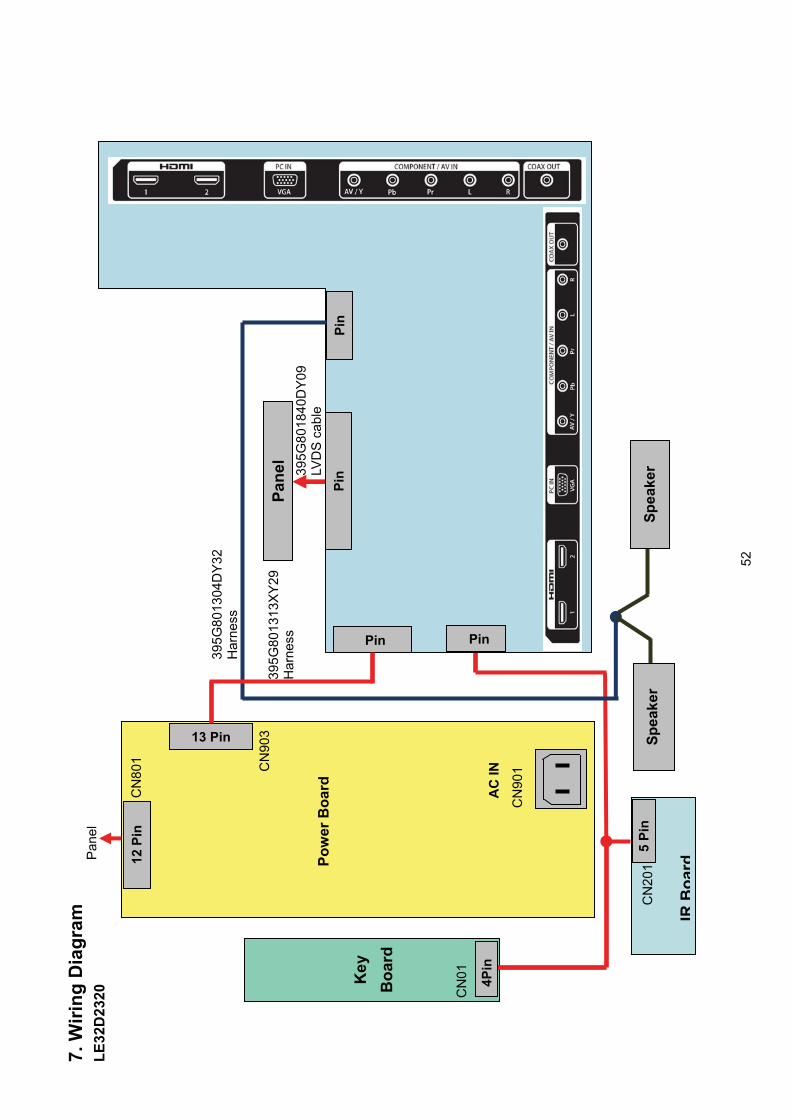
52
7. W
iring
Dia
gram
LE
32D
2320
Spea
ker
Spea
ker
395G
8018
40D
Y09
LVD
S c
able
Pane
l
Pin
395G
8013
04D
Y32
Har
ness
Pow
er B
oard
IRB
oard
CN
201
Key
B
oard
Pin Pin
CN
801
AC
IN
CN
901
CN
01
13 Pin
CN
903
Pan
el
12 P
in
4Pin
5 Pi
n
Pin
395G
8013
13X
Y29
Har
ness
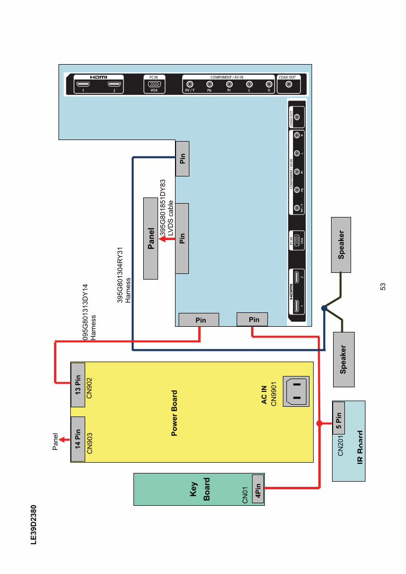
53
LE39
D23
80
395G
8013
04R
Y31
Har
ness
Spea
ker
Spea
ker
395G
8018
51D
Y83
LVD
S c
able
Pane
l
Pin
Pow
er B
oard
IRB
oard
CN
201
Key
B
oard
Pin Pin
CN
903
AC
INC
N99
01
CN
01
Pan
el
14 P
in
4Pin
5 Pi
n
Pin
095G
8013
13D
Y14
Har
ness
C
N90
213
Pin
54
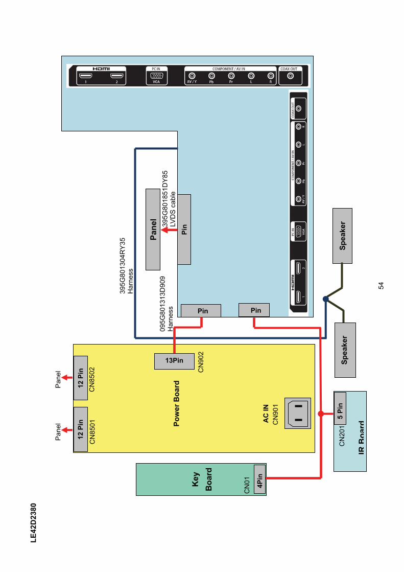
LE42
D23
80
Spea
ker
Spea
ker
395G
8018
51D
Y85
LVD
S c
able
Pane
l
Pin
395G
8013
04R
Y35
Har
ness
Pow
er B
oard
IRB
oard
CN
201
Key
B
oard
Pin Pin
CN
8501
AC
INC
N90
1
CN
01
Pan
el
12 P
in
4Pin
5 Pi
n
095G
8013
13D
909
Har
ness
CN
8502
12 P
in
13Pin
Pan
el CN
902

55
LE46
D23
80
Spea
ker
Spea
ker
395G
8018
51X
Y84
LVD
S c
able
Pane
l
Pin
395G
8013
04R
Y33
Har
ness
Pow
er B
oard
IRB
oard
CN
201
Key
B
oard
Pin Pin
CN
8502
AC
INC
N90
1
CN
01
Pan
el
4Pin
5 Pi
n
Pin
095G
8013
13D
909
Har
ness
13Pin
CN
902
12Pi
n
56
8. S
chem
atic
Dia
gram
8.
1 Po
wer
Boa
rd
LE32
D23
20
715G
5508
P010
0000
2S
+24V
C91
3310
0N 5
0V
12
FB
9101
BE
AD
R91
0710
K O
HM
+-5
% 1
/8W
ON
/OF
F
DIM
+12V
Q91
07P
1604
ETF
5.2V
5.2V
1
5.2V
R91
05
10 O
HM
1/8
W
R92
02
100
OH
M 1
%
C91
471u
F
R91
541K
1/8
W
2
1
3
4
-+
BD
901
TS6B
06G
-05-
X0
1 2 3 4
HS
9101
HE
AT
SIN
K
C91
262.
2nF
630
V
24V
_A
+12V
C9
13
21
00
N 5
0V
R9
12
222
0 O
HM
1/4
W
R9
12
022
0 O
HM
1/4
W
C9
12
71
00
N 5
0V
R9
12
122
0 O
HM
1/4
W
R91
5910
R
C9
12
510
00pF
630
V
Q91
142S
B11
24S
-TD
-E
+
C91
35N
C
1 2 3 4
HS
9102
HE
AT
SIN
K
5.2V
1
5.2V
1
C99
07
470N
F 3
05V
OV
P
R91
5020
0K +
-1%
1/4
W
C93
1622
0PF
250
V
OV
P
R91
1010
OH
M 1
/4W
R91
67N
C
C99
01
470N
F 3
05V
RV
9901
TVR
1456
1KF
AO
ZF
1 2 3
HS
9103
SH
IELD
R99
01
390K
R91
110.
24 o
HM
2W
1
2
3
D91
04F
MW
-215
6
C91
1947
pF
C93
151N
F 2
50V
12
FB
9103
BE
AD
R91
393.
9K 1
/8W
R99
03
390K
IC91
05A
S43
1AN
-E1
1 2
ZD
9106
P6K
E27
A
R91
2511
K 1
/8W
1%
A
C91
141u
F
B
BA
Q91
11
PM
BS
3904
21589 10 11 12 13 14 15 16
T9101
PO
WE
R X
'FM
R
SG
901
DS
PL-
501N
-A21
F
PS
_ON
R91
69
330R
1/8
W 5
%
C99
0647
pFNC
1
D1
2
D1
3
NC
4N
C5
D2
6D
27
NC
8
IC99
01C
AP
004D
G
C99
03
100P
F 2
50V
C99
02
1NF
250
V
BO
OT
1
VIN
2
EN
3
SS
4
PH
8
GN
D7
CO
MP
6
VS
NS
5
IC81
04 TPS
5423
1DR
OTP
1
CO
MP
2
CS
3
GN
D4
OU
T5
VC
C6
HV
8
IC91
01LD
7750
RG
R
SG
902
DS
PL-
501N
-A21
F
change type_1124change type_1124
1 2
4 3
L9902
30M
H
12
D91
06
SM
340A
C91
1010
00pF
630
V
soft start >20ms
C99
05
100P
F 2
50V
C99
04
1NF
250
V
R91
135.
1 O
HM
1/4
W
12
43L9901 30M
H
OE
M M
OD
EL
Siz
e
Rev
Dat
eS
heet
of
TPV
MO
DE
L
PC
B N
AM
E
T P
V
( T
op
V
icto
ry
E
lect
roni
cs
C
o .
,
Ltd.
)
Ke
y C
ompo
nent
Cus
tom
12
Tues
day
, A
pril
17,
2012
01.P
OW
ER
Bas
ic o
n G
5259
-P0C
C91
28
100N
50V
C91
4810
00pF
630
V
24V
_A
R9
14
83K
OH
M 1
%
C91
1510
0N 5
0V
+C
9113
470u
F 1
6V
1
2
3
D91
07F
MXA
-220
2S
R91
1647
OH
M 1
/4W
C91
30N
C
R9
10
48
2K
OH
M +
-5%
2W
S
R9
15
12K
43 1
/8W
1%
R91
1547
OH
M 1
/4W
R91
29
10K
OH
M +
-5%
1/8
W
C91
042.
2NF
+
C91
394.
7UF
50V
R91
026.
8K 1
/4W
R91
0647
OH
M +
-5%
1/8
W
D91
01P
R10
07
IC9
10
3K
IA4
31
A-A
T/P
C91
0510
0N 5
0V
1 2
4 3
IC9
10
2P
S2
56
1D
L1
-1
R91
016.
8K 1
/4W
R9
11
23.
3 O
HM
1/4
W
+C
9116
270U
F 2
5V
12
D9102
SS
0520
R91
3710
0K 1
/8W
1%
R91
036.
8K 1
/4W
1 2
tN
R99
01N
TCR
R91
52N
C
+C
9136
NC
+C
9103
NC
R91
35
100K
1/8
W 1
%
+C
9131
470U
F 3
5V
+C
9120
330U
F 3
5V
+12V
C91
4610
00pF
630
V
12
D9110
SS
0520
24V
_B
R91
5847
OH
M 1
/4W
24V
_B
C91
491N
F
12
CN
904
NC
/CO
NN
C91
34
100N
50V
R91
47
2K O
HM
C91
1710
0N 5
0V
L910
13.
5uH
24V
_A
R91
5347
0 O
HM
+24V
1
D91
03P
R10
07
+24V
1
C9
11
210
0N 5
0V
+ C91
1133
0UF
16V
12
FB
9104
BE
AD
1234
F90
1
FU
SE
12
FB
9105
BE
AD
12345678910111213
CN
903
CO
NN
1 2D
9109
RB
160M
1 2
D91
08
RB
160M
R91
66 NC
1 2
D91
05
RB
160M
L910
247
uH
12
ZD
9103
BZ
T52-
B6V
2Q
9108
2N70
02
Q91
052N
7002
12
ZD
9104
BZ
T52-
B9V
1
Q91
12N
C
12
ZD
9105
BZ
T52-
B16
R91
1839
K 1
/8W
1%
12
ZD
9107
BZ
T52-
B39
+C
9107
47U
F 5
0V
C99
08
470P
F 2
50V
+C
9144
56uf
450
V
+C
9145
56uf
45
0V
5.2V
C91
3810
0PF
50V
C91
2210
0N 5
0V
PS
_ON
R91
3410
0K 1
/8W
1%
R91
3310
K O
HM
+-5
% 1
/8W
Q91
01S
TF10
N65
K3
+24V
1
12
CN
901
SO
CK
ET
12
ZD
9101
MTZ
J27B
C91
2315
N 5
0V
C91
060.
1uF
50V
+24V
1
Q91
13N
C
C91
501N
FL
1
N2
CN
9902
CO
NN
PS
_ON
R91
5510
K O
HM
+-5
% 1
/8W
C91
180.
1uF
50V
R91
3810
0K 1
/8W
1%
C91
241n
F 5
0V
R91
2633
K O
HM
C91
2910
nF 5
0V
Q91
10P
MB
S39
06
R91
68N
C
5.2V
1
C91
37N
C
R91
405.
6K 1
/8W
R91
3639
0K O
HM
R9
14
327
K 1
/8W
1%
R9
14
43K
1/8
W +
/-1%
+C
9140
330U
F 5
0V
R91
4591
0 O
HM
1/8
W
+C
9141
330U
F 5
0V+
C91
4233
0UF
50V
+C
9143
330U
F 5
0V
12
FB
9102
BE
AD
R91
65N
C
R9
15
6 4
7KO
HM
+-1
% 1
/8W
R9109
470O
HM
+-5
% 1
/8W
1 2
FB
9106
BE
AD
PS
_ON
L910
33.
5uH
5.2V
R91
5733
K 1
/8W
5%
R91
70
330R
1/8
W 5
%
C91
0922
N 5
0V
+C
9101
NC
+C
9102
NC
R91
1933
0K 1
/8W
5%
R9
14
6 1
.5K
OH
M +
-1%
1/8
W
C91
0847
0P 5
0V
R92
01
100
OH
M 1
%
R91
1775
0 O
HM
1/8
W
R91
0810
0KO
HM
+-5
% 1
/8W
R91
1447
OH
M 1
/4W
57
123456789101112
CN
801
CO
NN
C81
101N
F
R81
2115
R
1%
R81
3715
R 1
%
SLP
R81
3815
R 1
%
VAD
JVBJ
T
VLED
+
OEM
MO
DEL
Size
Rev
Dat
eS
heet
of
TPV
MO
DEL
PCB
NAM
E
T P
V (
Top
V
icto
ry
Ele
ctro
nics
C
o . ,
Lt
d. )
Key
Com
pone
nt
B
22
Tues
day,
Apr
il 17
, 201
2
02.L
ED
DR
IVE
RN
EW-P
0A
Q81
082N
3904
Q81
092N
3904
Q81
102N
3904
R81
3915
R 1
%
Q81
112N
3904
VLE
D+
+C
8102
100U
F 63
V
R81
3615
R 1
%
+C
8113
100U
F 63
V
C81
171N
F
LED
3LE
D1
LED
4LE
D2
LED
2
LED
3
LED
1
LED
4
5.2V
LED
1LE
D2
LED
3
VSET
R81
174K
3 +-
1% 1
/8W
C81
181N
F
+12V
+24V
+12V
VLE
D+
1
2
3
D81
01
MBR
D10
150D
C81
1547
pF
C81
1647
pF
Q81
122N
3904
Q81
132N
3904
Q81
142N
3904
Q81
152N
3904
R81
0410
OH
M 1
/8W
R81
08
330R
1/8
W 5
%
C81
031u
F
Q81
022N
3904
R81
052R
2 +-
5% 1
/8W
Q81
032N
3904
R81
1318
R 1
%
R81
0610
K 1
/4W
R81
03
0 O
HM
1/4
W
SLP
R81
1610
0K 1
% 1
/4W
12
D81
02
RB1
60M
R81
1010
0K 1
% 1
/4W
R81
1915
0K 1
/8W
5%
C81
0510
0N 5
0V
C81
11N
C
C81
0910
0N 5
0V
R81
1118
K 1
/8W
5%
C81
12N
C
VAD
J
Q81
042N
3904
VBJT
Q81
052N
3904
Q81
062N
3904
Q81
072N
3904
3
12D
8103
BA
V99
3
12D
8108
BA
V99
3
12D
8107
BA
V99
3
12D
8105
BA
V99
3
12D
8104
BA
V99
3
12D
8106
BA
V99
+C
8101
330U
F 3
5V
R81
181M
1/6
W 5
%
C81
0410
0N 5
0V
R81
070.
07R
EN1
DIM
2
GM
3
VFB
4
VSET
5
OVP
6
RT
7C
S8
GN
D9
VMO
S10
VCC
11VB
JT12
VAD
J13
SLP
14IC
8501
PF7
001S
R81
0151
K 1
% 1
/8W
C81
0810
N 5
0V
C81
1410
N 5
0VR
8122
15R
1%
2
4
L810
1
33U
H
R81
2315
R 1
%R
8124
15R
1%
VFB
LED
4
R81
2515
R
1%R
8126
15R
1%
LED
5
VSET
R81
2715
R 1
%
Q81
01AO
D41
26
LED
6LE
D6
VFB
R81
2815
R 1
%
LED
5
LED
5
DIM
LED
6
R81
3215
R 1
%
ON
/OF
F
C81
061N
F
R81
0215
0K 1
/8W
58
LE39
D23
80
715G
5193
P010
0000
2H
C85
04
1uF
Q85
25TK
12A1
0K3
ON
/OFF
DIM
LED
-CO
MP
C85
21N
C
D85
12
MBR
F101
00C
T
1
2
3
LED
-S
LED
-CO
MP
LED
-1
IC85
02
PF77
00S
1 2 3 45678
DIM
EN VCC
LED
GN
DIS
ETGM
CO
MP
IC85
03
PF77
00S
1 2 3 45678
DIM
EN VCC
LED
GN
DIS
ETGM
CO
MP
LED
-2
LED
-4
LED
-4+1
2V
LED
-6
LED
-CO
MP
IC85
04
PF77
00S
1 2 3 45678
DIM
EN VCC
LED
GN
DIS
ETGM
CO
MP
DIM
R85
5368
0K 1
%
IC85
05
PF77
00S
1 2 3 45678
DIM
EN VCC
LED
GN
DIS
ETGM
CO
MP
ON
/OFF
R85
04
11K
1/8W
1%
R85
07
165K
1%
LED
-1
R85
4727
OH
M
IC85
06
PF77
00S
1 2 3 45678
DIM
EN VCC
LED
GN
DIS
ETGM
CO
MP
R85
01
11K
1/8W
1%
R85
4810
K 1/
8W
R85
1510
0K 1
/4W
R85
50
1.5K
1/8
W
C85
03
1uF
LED
-CO
MP
L850
25u
H
+
C85
1115
0UF
35V
R85
4947
0 O
HM
1/4
W
+12V
DIM
R85
520.
05R
LED
-5
+
C85
1022
0UF
100V
C85
23
0.47
UF
50V
C85
01
1uF
DIM
C85
05
1uF
+12V
L850
125
UH
1
2
C85
16N
C
R85
03
11K
1/8W
1%
+24V
R85
06
11K
1/8W
1%
C85
22
0.47
UF
50V
LED
-CO
MP
R85
02
11K
1/8W
1%
<Doc
><R
evC
ode>
<Titl
e>
A3
11
Tues
day,
Dec
embe
r 20,
201
1
Title
Size
Doc
umen
t Num
ber
Rev
Dat
e:Sh
eet
of
LED
-3
C85
06
1uF
ON
/OFF
LED
-FB
R85
5124
0K O
HM
1%
C85
02
1uF
LED
-5
+12V
CN
8501
CO
NN
123456789101112
+
C85
0912
UF
160V
R85
05
11K
1/8W
1%
+C
8507
47U
F 50
V
R85
5439
K 1/
8W 1
%
LED
-CO
MP
LED
-S
+12V
ON
/OFF
ON
/OFF
IC85
50
PF79
00S
1 2 3 45678
FB GM
RT
CS
DIM
GN
DO
UT
VCC
+12V
LED
-CO
MP
R85
1310
0K 1
/4W
DIM
LED
-6
ON
/OFF
+12V
DIM
+12V
C85
1447
0P 5
0V
R85
1410
0K 1
/4W
LED
-FB
+
C85
1215
0UF
35V
C85
0810
0N 5
0V
LED
-2
IC85
01
PF77
00S
1 2 3 45678
DIM
EN VCC
LED
GN
DIS
ETGM
CO
MP
C85
131N
50V
LED
-S
LED
-3
DIM
59
!R
9903
330K
1/4
W
PS_
ON
!R
9155
10K
1/8
W
ZD93
05G
DZ
J15B
12
+
C93
4033
0UF
16V
Q91
03N
C
1
2
3
CN
9902
NC1
2
L990
2
12M
H
1 2
4 3
1.0A2
22
Wed
nesd
ay, D
ecem
ber 2
1, 2
011
<>
02.P
ower
circ
uit
OEM
MO
DE
LS
ize
Rev
Dat
eS
heet
of
TPV
MO
DEL
PC
B N
AME
T P
V
( Top
V
icto
ry
Ele
ctro
nics
C
o . ,
L
td. )
Key
Com
pone
nt
R93
6622
K 1
/8W
C91
531U
25V
!
!
T910
1
POW
ER
X'F
MR
1245
678 911 1210
C91
7010
0N 5
0V
C99
0122
0PF
250
V
R91
48N
C
C91
484.
7uF
25V
R93
378K
2 1/
8W 1
%
ZD
9352
NC
12
C98
262N
2 50
V
FB9
301
BEA
D
12
R93
244R
7 1/
4W 5
%
MSS
t
NR
9901
NTC
R
12
VC
C1
!
R91
8027
K 1
/8W
1%
VBo
ot
!
R91
462K
43 1
/8W
1%
C93
38
1NF
D91
14U
F101
0G
DIM
ZD
9801
GD
ZJ4.
7B
1 2
IC91
07A
S431
AZTR
-E1
ZD
9104
GD
ZJ15
B
12
Q91
11
NC
C98
04
470P
F1K
V
C91
6510
0N 5
0V
C91
44N
C
+C
9830
10U
F 50
V
Q93
06P
MBS
3904
C98
2910
0N 5
0V
CN
9903
NC
1 2L N
+24V
!
R99
04N
C
R91
761.
5K 1
/4W
R98
1468
0K O
HM
+-1
% 1
/4W
VCC
1
B-
R93
2710
0K 1
/4W R
9302
2 O
HM
1%
R93
6410
K 1/
8W
R98
29
0.1R
C98
201U
F 45
0V
R93
6522
0 O
HM
1/4
W
+C
9147
10U
F 5
0V
R98
0930
R +
-1%
1/8
W
!
D91
17
FMW
-215
6
1
2
3
R93
18
1M5
1/4W
5%
R98
15
680K
OH
M +
-1%
1/4
W
R91
583.
9K 1
/4W
IC93
04A
S431
AZTR
-E1
B1+
C99
05N
C
IC93
08
PC12
3X8Y
FZO
F
1 2
4 3
R99
0233
0K 1
/4W
+12V
C99
08N
C
D91
16
FM
EN-2
308
1
2
3
BO
X
CN
902
CO
NN
12345678910111213
C91
5456
0P 5
0V
C91
5933
0NF
50V
C93
3322
0NF
B+
C99
091N
F 2
50V
D98
03S
S052
01
2
D91
10N
C
C98
2710
0P 5
0V
IC93
03P
C12
3X8Y
FZO
F
1 2
4 3
R91
5447
OH
M +
-5%
1/8
W
+12V
+C
9172
NC
C99
0222
0PF
250V
!
+
C93
4127
0UF
25V
D91
13S
S052
01
2
R99
0133
0K 1
/4W
!
R98
0722
0 O
HM
1/4
W
D93
05
PG
1010
R
R91
39N
C
RV9
901
NC
R93
672.
7K 1
/8W
R93
2510
0K 1
/4W
+C
9336
10U
F 50
V
!
! C99
11
470N
F 3
05V
5V
R93
17
1M5
1/4W
5%
R91
12N
C
+
C91
6827
0UF
25V
-+
BD
9901
TS10
B06
G-0
6-X0
2
1
3
4
+
C98
0147
UF
450
V
+12V
!
R93
3422
0 O
HM
1/4
W
L930
45u
H
L910
65u
H
VC
C
R93
2810
0K 1
/4W
R91
421M
1%
1/4
W
DIM
C91
5210
PF 3
KV
SG
9901
NC
C85
1710
00pF
630
V
FB99
03BE
AD
12
B1+
C91
5718
NF
R91
5110
R 1
/8W
5%
R91
130R
05 1
/4W
R91
725.
1K 1
/4W
C91
11N
C
C91
500.
47U
F 50
V
Q98
02N
C
C98
2810
0N 5
0V
IC93
01A6
069H
1 2 3 4578
S/O
CP
BR GN
DFB
/OLP
VC
C
D/S
TD
/ST
!
R93
23
4.7
MO
HM
+-5
% 1
/4W
ZD
9101
NC
12
+
C91
7127
0UF
25V
!
R98
17N
C
!
L980
1
300U
H
1
3
R98
1013
K O
HM
1%
L990
1
12M
H
12
43
Q93
052S
D16
24T-
TD-E
VBo
ot
+12V
+C
9337
100U
F 5
0V
R98
190R
05 1
/4W
VC
C1
R91
715.
1K 1
/4W
+
C91
6927
0UF
25V
C99
0633
0PF
250
V
+
C91
6415
0UF
35V
D91
18
NC
12
+24V
C93
3247
0PF1
KV
D91
19
NC
12
R91
01
160O
HM
+-5
% 1
/8W
C91
4910
0N 5
0V
+24V
C93
4210
0N 5
0V
R91
470R
05 1
/4W
R93
2610
0K 1
/4W
C98
2422
N 5
0VC
9343
0.22
uF 5
0V
R91
11N
C
B-
!
R91
40N
C
C91
511U
25V
B+
24V
!
C98
21N
C
C99
0433
0PF
250V
+C
9371
10U
F 50
V
R85
11
10K
1/4W
R93
3147
OH
M 1
/4W
IC98
01
R2A
2011
3ASP
1 2 3 45678
FB
CO
MP
RT
VR
EFC
SG
ND
OU
TV
CC
R91
44
1M 1
% 1
/4W
ZD
9103
GD
ZJ2
7B
12
R93
387K
5 1/
8W +
/-1%
+
C98
03N
C
5V
C91
551N
50V
R91
6010
K 1
/4W
F99
01F
US
E
R91
593.
3K 1
/4W
+C
9163
1000
uF 3
5V
R93
361K
1/8
W
R91
431M
1%
1/4
W
!IC
9101
SSC
9512
S-TL
1 2 3 4 5 6 7 8 9101112131415161718
Vse
nV
ccF
BG
ND
Css
OC
RC
Reg
RV
CO
MVG
LN
CN
CVB
VS
VG
HN
CN
C
T930
1PO
WE
R X
'FM
R1 2 3 45
7 9
D93
07PG
1010
R
R98
0620
0K 1
/8W
ZD
9102
NC
12
R98
18N
C
C91
4510
0N 5
0V
CN
9901
SO
CK
ET
12
!D
9306
1N41
48
!
C99
0733
0PF
250
V
C93
3410
N 5
0V
C85
1810
00pF
630
V
!
Q91
01
TK10
A50D
R91
632K
1/8
W 1
%
D91
12SS
0520
12
+24V
VC
C1
DE
T
!
C93
3510
0N 5
0V
C99
10
470N
F 30
5V
R93
012
OH
M 1
%
R91
4513
K O
HM
1%
!
C91
4610
0N 5
0V
R93
3047
OH
M 1
/4W
IC99
01
NC
1 2 3 45678
NC
D1
D1
NC
NCD2
D2
NC
D91
09N
C
!
C93
7210
0N 5
0V
PS_
ON
SG99
02N
C
R98
01
0.07
R
R98
0830
OH
M 1
/4W
R93
2056
0K 1
/8W
R91
751.
5K 1
/4W
Q91
02TK
10A5
0D
5V
BOX
MSS
C93
31
1NF
R91
6124
K 1/
8W 1
%
+12V
C91
56
100P
F1KV
ON
/OFF
L910
55u
H
5V
D93
04
PG10
10R
VC
C
D93
09N
C
R85
12
10K
1/4W
ZD
9351
GD
ZJ6
.2B
12
!
!
ON
/OF
F
D98
02IN
5408
G-0
4
+24V
!
R98
0524
0K 1
/8W
5%
R93
35
3K3
1/8W
5%
+24V
R93
19
1M5
1/4W
5%
!
FB9
802
BEA
D
12
!R
9816
680K
OH
M +
-1%
1/4
W
R91
5310
K 1
/8W
VCC
1
R98
1310
K 1
/4W
Q98
01TK
13A6
0D
R91
491K
1/8
W
C99
0347
0PF
250
V
ZD93
03
GD
ZJ1
5B
12
C98
2547
N 5
0V
D98
01F
MN
S-1
106S
FB99
04BE
AD
12
+
C98
0247
UF
450V
FB99
09BE
AD
12
D93
08
FM
W-2
156
1
2
3
R91
5247
OH
M +
-5%
1/8
W
CN
903
NC
1234567891011121314
IC91
06PC
123X
8YF
ZOF
1 2
4 3
!!
C91
58N
CD
ET
60
LE42
D23
80/L
E46D
2380
71
5G52
46P0
1W21
002S
P_O
K
C9162100N 50V
P_O
K
On/
Off
C98
33
47PF
C93
45
NC
D93
07FR
103
R93
378K
2 1/
8W 1
%
D93
05
FR
107
SB+
C99
12
470P
F 25
0V
EN
R93
2056
0K 1
% 1
/8W
SG99
03D
SPL-
501N
-A21
F
Q98
02N
CR
9819
NC
C9832NC
R98
110R
05
12V
12
ZD93
03
GD
ZJ15
B
R99
04N
C
HEAT
SINK
(Q91
01,Q
9102
)
R99
05N
C
NC
1
D1
2
D1
3
NC
4N
C5
D2
6D
27
NC
8
IC99
01N
C
HEAT
SIN
K(BD
9901
)
R91
6124
K 1/
8W 1
%
R91
632K
1/8
W 1
%
C99
0647
0PF
250V
C99
0747
0PF
250V
R98
0710
0 O
HM
1/4
W
6
1
L980
145
0UH
R91
8027
K 1/
8W 1
%
R93
09N
C
R93
10N
C
B1+
1 2 3 5
6 7 9 10
4
T930
1
POW
ER X
'FM
R
R91
715.
1K 1
/4W
12
D91
12SS
1060
FL
C99
1033
0NF
305V
R98
1016
K 1%
1/8
W
C99
1133
0NF
305
V
PS-O
n
R91
751.
5K 1
/4W
C91
7010
0N 5
0V
1 2 6 7
8 9 10 1112 1314 15
T91
01
PO
WE
R X
'FM
R
3 41 2
HS
9101
HE
AT S
INK
R93
0710
K 1%
1/4
W
12
ZD91
05G
DZJ
30B
C99
0347
0PF
250
V
1 2 3 4
HS9
301
HEA
T SI
NK
(D93
08)
C93
3510
0N 5
0V
FUSE5X20
F990
1FU
SE
R93
387K
5 1/
8W 1
%
On/
Off
5.2V
DV5
!
R91
43
NC
12 C
N90
1SO
CKE
T
R93
241K
1/8
W 1
%
R93
39N
C
Mai
n_ov
R93
41
NC
R91
38
1K 1
/8W
1%
R98
04N
C
R93
3147
OH
M 1
/4W
FB1
CO
MP
2
RT
3
VREF
4C
S5
GN
D6
OU
T7
VCC
8IC
9801
R2A
2011
3ASP
1 2
4 3
IC93
03PC
123X
8YFZ
OF
R93
40
NC
R93
171.
5M 1
% 1
/4W
R93
45
0R05
1/8W
5.2V
R91
4516
K9 1
/8W
1%
24V
R93
3422
0 O
HM
1/4
W
C91
511U
F
12
ZD93
01G
DZJ
18B
C98
201U
F 45
0V
C91
531u
F
5.2V
C93
330.
47U
F 50
V
R93
110
OH
M 1
/8W
+C
9801
47U
F 4
50V
2
1
3
4-
+
BD99
01
KBJ1
008G
-FU
12V
R98
0656
K 1
/8W
C98
2422
N 5
0V
C91
4410
0N 5
0V
R91
5110
OH
M
R91
5920
K 1/
4W
R91
41
0.1R
C91
5722
NF
R93
29
0.1R
C98
2522
0N 5
0V
R93
181.
5M 1
% 1
/4W
C93
4210
0N 5
0V
12V
C98
271N
50V
C91
5933
0NF
50V
R91
47
470
OH
M 1
/8W
R93
361K
1/8
W 1
%
R91
401K
1/8
W 1
%
R91
49
470
OH
M 1
/8W
12
FB9
904
BEA
D
!
R93
4622
0R
change to 150uF
C98
262N
2 50
V
R91
725.
1K 1
/4W
R91
53
10K
1/8W
1%
R91
735.
1K 1
/4W
D91
091N
4148
R91
745.
1K 1
/4W
SG99
02D
SPL-
501N
-A21
F
SG99
05D
SPL
-501
N-A
21F
!
SG99
04D
SPL-
501N
-A21
F
S/O
CP
1
BR2
GN
D3
FB/O
LP4
VCC
5D
/ST
7D
/ST
8
IC93
01A
6069
H
IC93
04AS
431A
ZTR
-E1
D98
01
FMN
S-11
06S
5.2V
R93
322R
2 +-
5% 1
/4W
R98
0810
R 1
/8W
5% C
9828
100N
50V
R91
761.
5K 1
/4W
R91
771.
5K 1
/4W
C91
712.
2nF
630V !
Q93
05
MM
BT3
906
PNP
R93
35
3K3
1/8W
5%
R91
60
1K 1
/8W
1%
R91
3910
0 O
HM
1%
R91
0118
0R 1
%
VCC
1
change to 8.5mm
change to 8.5mm
VCC
R93
0810
K 1/
8W 1
%
DIM
12
ZD91
01G
DZJ
30B
C93
381N
F
DV5
C93
311N
F
12
ZD91
07BZ
T52-
B22
R98
1310
K 1/
4W
R98
141M
1/4
W 1
%
R98
0920
0 O
HM
1/4
W
Q98
01TK
13A6
0D
R98
1568
0K O
HM
+-1
% 1
/4W
R93
42
NC
24V
24V
R98
16
680K
OH
M +
-1%
1/4
W
R93
0410
0K 1
/8W
1%
R98
1710
0K +
-1%
1/4
W
R93
3047
OH
M 1
/4W
R91
48N
C
12
ZD91
02G
DZJ
15B
24V
Q91
06
MM
BT39
06 P
NP
C93
4322
0N 5
0V
R91
462K
43 1
/8W
1%
C91
500.
47U
F 5
0V
OEM
MO
DEL
Size
Rev
Dat
eSh
eet
of
TPV
MO
DEL
PCB
NAM
E
T P
V
( Top
V
icto
ry
Ele
ctro
nics
C
o . ,
Lt
d. )
Key
Com
pone
nt
CA2
13
<>
POW
ER C
IRC
UIT
715G
5246
P010
0000
2H
Satu
rday
, M
ay 0
5, 2
012
1 2
4 3
IC91
06PC
123X
8YFZ
OF
R91
5610
K 1/
8W 1
%
D93
061N
4148
BO
X
+C
9830
10U
F 50
V
1
2
3
D93
08
FMW
-215
6
12
FB
9801
BE
AD
12
FB
9802
BE
AD
Q91
01TK
10A
50D
Q91
02TK
10A
50D
R91
585.
6K
12
FB90
2BE
AD
VBoo
t
B1+
D98
02IN
5408
G-0
4
R93
011.
0R
B1+
C91
56
100P
F1K
V
D145
T60P
7_5-
1_2-R
D145T6
0P7_
5-1_
2-R
L930
4
3UH
!
12
D91
13SS
1060
FL
BOX
R93
0320
K 1/
4W
L910
33U
H
12
D98
03SS
1060
FL
C91
4910
0N 5
0V
Q93
04 NC
C91
551N
50V
R93
43
NC
12V
C93
341N
50V
L910
63U
H
+C
9344
470U
F 25
V
VBoo
t
Vsen
1
Vcc
2
FB3
GN
D4
Css
5
OC
6
RC
7
Reg
8
RV
9C
OM
10VG
L11
NC
12N
C13
VB
14V
S15
VGH
16N
C17
NC
18IC
9101
SSC
9522
S
C99
0810
0PF
250V
C99
0910
0PF
250V
!!
12
D93
01SS
1060
FL
R98
010.
07R
!
R91
11
0 O
HM
+-5
% 1
/8W
C98
0347
0PF1
KV
C91
5210
PF
1
2
3
D91
15F
ME
N-2
308
HEAT
SIN
K(Q9
801,
D980
1)
C91
6510
0N 5
0V
VCC
1
R93
332K
1/8
W 1
%
+C
9302
22U
F 50
V
VCC
VCC
1
5.2V
1 2D
9302
SS1
060F
L
C91
5456
0P 5
0V
Mai
n_ov
Q93
03S
MA
LLTR
AN B
TC46
72M
3 5A
50V
0.6
W S
OT-
89
12
43L9
901
12M
H
C93
0110
0N 5
0V
R91
52
47O
HM
+-5
% 1
/8W
D91
101N
4148
IC91
07AS
431A
ZTR
-E1
1 2
4 3
L990
3
12M
H
R91
5447
OH
M +
-5%
1/8
W
+C
9161
560U
F 35
V
C91
4610
0N 5
0V
1 2
4 3
IC93
02
PC
123X
8YFZ
OF
D91
14U
F400
7
R-
C91
58N
C
C91
4510
0N 5
0V
R-
1 2
tN
R99
02
NTC
R
1 2
tN
R99
01N
TCR
HEAT
SINK
(D81
20,Q
8101)
+C
9341
470
16V
R98
0520
0KO
HM
1/8
W +
/-5%
+C
9340
470U
F 10
V
RV9
901
TVR
1456
1KFA
OZFRV9
902
TVR
1456
1KFA
OZF
+24V
R-
C91
484.
7UF
10V
1
2
3
D91
16FM
EN-2
308
VC
C1
HEAT
SINK(D
9115
,D91
16)
R98
18N
C
12
ZD93
04G
DZJ
6.2B
R91
421.
5M 1
% 1
/4W
12345678910111213
CN
902
CO
NN
R91
501.
5M 1
% 1
/4W
R91
441.
5M 1
% 1
/4W
+C
9336
10U
F 5
0V
12
FB
9805
BE
AD
C99
01N
C
+C
9337
47U
F 50
V
R91
55
NC
+C
9802
47U
F 45
0V
+C
9147
22U
F 50
V
R93
2510
0K
R93
26
100K
R93
2710
0K
R93
28
100K
!
!
C99
1347
0PF
250V
!
!
!!
!!
!
!!
!
!
! !
!
!
!
!
!
!
!
!
!
R91
785.
1K 1
/4W
!
Q91
03PM
BS39
04
12
ZD91
04G
DZJ
15B
!
!
!
1 2 3 4
HS9
103
HEA
T SI
NK
R2A20113A
R93
191.
5M 1
% 1
/4W
D93
04
FR
107
C98
2910
0N 5
0V
1 2
ZD91
06BZ
T52-
B5V1
+C
9163
470U
F 2
5V+
C91
6847
0UF
25V
+C
9169
470U
F 25
V
+C
9804
47U
F 4
50V
24V-
LED
3 41 2
HS9
102
HEA
T S
INK
R99
011M
OH
M +
-5%
1/2
W
123456789101112
CN
903
NC
PS-O
n
R93
23
4.7M
OH
M +
-5%
1/4
W
12
FB98
03BE
AD
24V
+C
9160
560U
F 35
V
Q91
04TK
2P60
D
C99
0515
0PF
250
V
R91
641K
+C
9164
330U
F 35
V
VC
C1
+C
9805
47U
F 45
0V
DV5
Q93
01N
C
DIM
R93
0210
0K 1
/6W
5%
Q93
022N
7002
K
On/
Off
R91
6510
KOH
M
1 2 3 4
HS9
801
HEA
T SI
NK
1 2 3 4
HS9
901
HEA
T SI
NK
24V
R91
0210
OH
M
5.2V
R91
03
10 O
HM
R93
062K
1/8
W 1
%
12
FB98
04BE
AD

61
OEM
MO
DEL
Size
Rev
Dat
eS
heet
of
TPV
MO
DEL
PC
B N
AME
T P
V
( To
p
Vic
tory
E
lect
roni
cs
Co
. ,
Ltd.
)
Key
Com
pone
nt
CA
23
<>
24V
to V
LED
(D
C/D
C)
715G
5246
-P0C
-000
-003
0
Wed
nesd
ay, F
ebru
ary
29, 2
012
1 2
D81
18S
S106
0FL
R93
15N
C
R81
770R
05
R81
4782
K +
-1%
1/8
W
R81
5710
K 1
/8W
1%
R93
44N
C
R93
22N
CC
9346
NC
R81
5847
OH
M +
-5%
1/8
W
R81
750.
03R
R81
76N
C
Q81
01A
OTF
454F
L
1
2
3
D81
20
FM
E-2
20B
R81
6110
OH
M
R81
63 4
70K
OH
M +
-1%
1/8
W
C81
06N
C
R81
4530
0K O
HM
1%
Q93
08N
C
R81
4482
K +
-5%
1/8
W
C81
1110
0N 5
0V
R81
53
0 O
HM
1/8
W
C81
1347
0N 5
0V
R81
4120
K 1
% 1
/8W
12
ZD81
03
NC
R93
12N
C
C81
051N
50V
R81
5410
0K
R93
13N
C
R93
21
NC
FB 1
GM 2
RT 3
CS 4DIM5 GND6 OUT7 VCC8
IC81
03 LD7400GS
R81
5510
0K
R81
4830
K 1
/8W
1%
Q93
06N
C
R81
5610
0K
R93
160R
051/
8W
C81
191N
50V
R81
621K
1/8
W 1
%
LED
-CO
MP
24V
-LE
D
12V
VLE
D
DIM
EN
12V
_LE
D
On/
Off
12V
12V
_LE
D
+C
8108
100U
F 1
00V
+
C81
21
22U
F 50
V
+C
8118
100U
F 1
00V
1
2
L810
133
UH
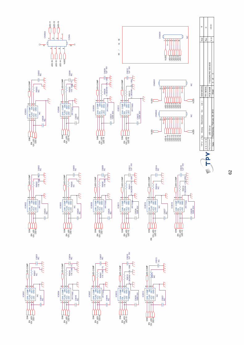
62
OE
M M
OD
ELSi
ze
Rev
Dat
eS
heet
of
TPV
MO
DEL
PCB
NA
ME
T P
V
( Top
V
icto
ry
Ele
ctro
nics
C
o .
, L
td.
)
Key
Com
pone
nt
CB
33
<>
.LED
Driv
er71
5G52
46-P
0C-0
00-0
030
Wed
nesd
ay, F
ebru
ary
29, 2
012
C85
14N
C
DIM
1
EN2
VCC
3
LED
4G
ND
5IS
ET6
GM
7C
OM
P8
IC85
11
PF77
00S
DIM
1
FLAG
2
VCC
3
LED
4G
ND
5IS
ET6
GM
7C
OM
P8
IC85
08
PF77
00S
C85
06N
C
R85
0911
.5K
OH
M +
-1%
1/8
W
R85
0811
K 1/
8W 1
%
C85
3110
0N 5
0V
DIM
1
FLA
G2
VC
C3
LED
4G
ND
5IS
ET
6G
M7
CO
MP
8IC
8504
PF77
00S
R85
01N
C
DIM
1
FLAG
2
VCC
3
LED
4G
ND
5IS
ET6
GM
7C
OM
P8
IC85
14
NC
R85
13N
C
R85
0711
K 1/
8W 1
%
C85
3210
0N 5
0V
R85
03N
C
C85
121U
F 1
6V
C85
17N
C
R85
0611
K 1/
8W 1
%
123456789101112
CN
8502
NC
C85
01N
C
DIM
1
EN2
VCC
3
LED
4G
ND
5IS
ET6
GM
7C
OM
P8
IC85
12
PF77
00S
R85
1111
.5KO
HM
+-1
% 1
/8W
C85
04N
C
C85
23N
C
C85
2610
0N 5
0V
R85
0411
K 1/
8W 1
%
1 2 3 4 5 6 7 8
CN
8504
NC
R85
1211
.5K
OH
M +
-1%
1/8
W
DIM
1
FLAG
2
VCC
3
LED
4G
ND
5IS
ET6
GM
7C
OM
P8
IC85
05
NC
C85
2010
0N 5
0V
C85
101U
F 16
V
C85
29N
C
DIM
1
FLA
G2
VC
C3
LED
4G
ND
5IS
ET
6G
M7
CO
MP
8IC
8501
NC
C85
02N
C
C85
07N
C
DIM
1
FLA
G2
VC
C3
LED
4G
ND
5IS
ET
6G
M7
CO
MP
8IC
8513
NC
C85
30N
C
C85
21N
C
DIM
1
EN2
VCC
3
LED
4G
ND
5IS
ET6
GM
7C
OM
P8
IC85
09
PF77
00S
R85
1611
.5KO
HM
+-1
% 1
/8W
R85
1011
.5K
OH
M +
-1%
1/8
W
R85
14N
CC
8513
NC
DIM
1
FLA
G2
VC
C3
LED
4G
ND
5IS
ET
6G
M7
CO
MP
8IC
8506
PF77
00S
12
34
56
78
9 10
CN
8503
CO
NN
C85
27N
C
C85
24N
C
123456789101112
CN
8501
NC
DIM
1
FLAG
2
VCC
3
LED
4G
ND
5IS
ET6
GM
7C
OM
P8
IC85
02
PF77
00S
DIM
1
EN2
VCC
3
LED
4G
ND
5IS
ET6
GM
7C
OM
P8
IC85
16
PF77
00S
C85
05N
C
R85
05N
C
C85
2810
0N 5
0V
C85
18N
C
R85
0211
K 1/
8W 1
%
DIM
1
EN
2
VC
C3
LED
4G
ND
5IS
ET
6G
M7
CO
MP
8IC
8510
PF7
700S
DIM
1
FLA
G2
VC
C3
LED
4G
ND
5IS
ET
6G
M7
CO
MP
8IC
8507
PF77
00S
C85
111U
F 1
6V
C85
161U
F 1
6V
C85
03N
C
C85
08N
CC
8519
NC
DIM
1
FLA
G2
VC
C3
LED
4G
ND
5IS
ET
6G
M7
CO
MP
8IC
8503
NC
C85
091U
F 1
6VC
8525
NC
LED
-CO
MP
EN
LED
-16
LED
-CO
MP
EN
DIM
EN12
V_LE
D
EN
LED
-5
12V_
LED
LED
-3
LED
-CO
MP
LED
-6
LED
-CO
MP
LED
-CO
MP
LED
-14
LED
-2
12V_
LED
LED
-CO
MP
LED
-16
12V_
LED
LED
-CO
MP
DIM
LED
-6
EN
EN
LED
-5
EN
LED
-CO
MP
LED
-CO
MP
LED
-CO
MP
VLE
D
12V_
LED
LED
-16
12V
_LE
D
DIM
12V_
LED
LED
-14
LED
-10
12V_
LED
LED
-3
VLED
VLED
LED
-3
LED
-1
LED
-4
12V_
LED
LED
-CO
MP
LED
-CO
MP
LED
-8
LED
-2
LED
-13
12V_
LED
LED
-CO
MP
VLE
D
LED
-2
LED
-14
DIM
LED
-13
VLE
DLE
D-9
VLE
D
DIM
12V
_LE
D
LED
-11
LED
-7
LED
-CO
MP
LED
-6
LED
-13
12V_
LED
DIM
LED
-4
LED
-CO
MP
DIM
DIM
12V_
LED
LED
-7
DIM D
IM
LED
-1
LED
-15
EN
LED
-11
DIM
DIM
EN
ENLED
-10
LED
-4
LED
-15
12V_
LED
ENEN
DIM
LED
-12
LED
-5
LED
-12
LED
-15
12V_
LED
EN
LED
-12
EN LE
D-9
EN
LED
-8
LED
-1
DIM
DIM
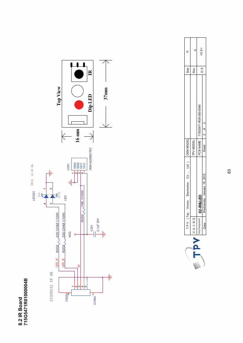
63
8.2
IR B
oard
71
5G54
71R
0100
0004
B
GN
D1
GN
D2
OU
T3
VCC
4
U20
1
IRM
-H63
6M3/
TR2
IR
033G
8032 5F
HR
C20
1
0.1u
F 50
V
VCC
R20
115
K 1
/10W
081G 14 24 EL
OEM
MO
DEL
Size
Rev
Dat
eSh
eet
of
TPV
MO
DEL
PCB
NAM
E
T P
V (
Top
V
icto
ry
Ele
ctro
nics
C
o . ,
Lt
d. )
Key
Com
pone
nt
AA
22
Wed
nesd
ay, J
anua
ry 1
8, 2
012
715G
5471
-R0A
-000
-004
0<
>02
-IR&
LED
R20
322
0 O
HM
1/1
0WLE
D_B
1 2 3 4 5
6 7
CN
201
CO
NN
LED
_R
1 234
RED
BLUE
LED
201
LED
R20
222
0 O
HM
1/1
0W
Dip
LED
Top
Vie
w
IR
16 m
m
37m
m
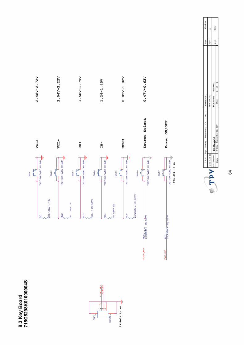
64
8.3
Key
Boa
rd
715G
5298
K01
0000
04S
FU
NC
_KE
YP
WR
-SW
33G8
032 4F H
R
Sour
ce S
elec
t
MENU
VOL-
VOL+
Powe
r ON
/OFF
CH+
CH-
OE
M M
OD
EL
Siz
e
Rev
Dat
eS
heet
of
TPV
MO
DE
L
PC
B N
AM
E
T P
V
( T
op
V
icto
ry
E
lect
roni
cs
C
o .
,
Ltd.
)
Key
Com
pone
nt
ACus
tom
22
Frid
ay,
Sep
tem
ber
02,
2011
715G
XXXX
<>
02-K
eypa
d
1.24
~1.4
5V
2.04
V~2.
22V
2.48
V~2.
72V
1.58
V~1.
79V
0.47
V~0.
63V
0.85
V~1.
02V
R05
750O
HM
+-1
% 1
/8W
R04
1K
1/8
W 1
%
R01
7K
5 1
/8W
+/-
1%
R03
1K
8 +
/-1%
1/8
W
R06
750O
HM
+-1
% 1
/8WR02
2K
7 1
/8W
1%
R07
750O
HM
+-1
% 1
/8W
SW
01
TAC
T S
W F
WR
D H
1.5M
M
1 2 3 4
6 5
CN
01
CO
NN
FU
NC
_KE
Y
PW
R-S
W
77G 607
2 FD
SW
02
TAC
T S
W F
WR
D H
1.5M
M
SW
03
TAC
T S
W F
WR
D H
1.5M
M
SW
04
TAC
T S
W F
WR
D H
1.5M
M
SW
05
TAC
T S
W F
WR
D H
1.5M
M
SW
06
TAC
T S
W F
WR
D H
1.5M
M
SW
07
TAC
T S
W F
WR
D H
1.5M
M


![21J-FG1RU SERVICE MANUALdocshare02.docshare.tips/files/25053/250532927.pdf · 21J-FG1RU 2 – 1 21J-FG1RU CHAPTER 2. IMPORTANT SERVICE NOTESService Manual [1] IMPORTANT SERVICE NOTES](https://img.pdfslide.net/doc/110x75/5e8cc490dc136f29fc5bd037/21j-fg1ru-service-21j-fg1ru-2-a-1-21j-fg1ru-chapter-2-important-service-notesservice.jpg)