Embed Size (px)
Citation preview

This is information on a product in full production.
July 2015 DocID5279 Rev 9 1/19
ULN2001, ULN2002ULN2003, ULN2004
Seven Darlington array
Datasheet - production data
Features• Seven Darlingtons per package
• Output current 500 mA per driver (600 mA peak)
• Output voltage 50 V
• Integrated suppression diodes for inductive loads
• Outputs can be paralleled for higher current
• TTL/CMOS/PMOS/DTL compatible inputs
• Inputs pinned opposite outputs to simplify layout
DescriptionThe ULN2001, ULN2002, ULN2003 and ULN 2004 are high voltage, high current Darlington arrays each containing seven open collector Darlington pairs with common emitters. Each channel rated at 500 mA and can withstand peak currents of 600 mA. Suppression diodes are included for inductive load driving and the inputs are pinned opposite the outputs to simplify board layout.
The versions interface to all common logic families: ULN2001 (general purpose, DTL, TTL, PMOS, CMOS); ULN2002 (14 - 25 V PMOS); ULN2003 (5 V TTL, CMOS); ULN2004 (6 - 15 V CMOS, PMOS).
These versatile devices are useful for driving a wide range of loads including solenoids, relays DC motors, LED displays filament lamps, thermal printheads and high power buffers.
The ULN2001A/2002A/2003A and 2004A are supplied in 16 pin plastic DIP packages with a copper leadframe to reduce thermal resistance. They are available also in small outline package (SO-16) as ULN2001D1/2002D1/2003D1/ 2004D1.
DIP-16L SO-16(Narrow)Plastic DIP-16L
www.st.com

Contents ULN2001, ULN2002, ULN2003, ULN2004
2/19 DocID5279 Rev 9
Contents
1 Diagram . . . . . . . . . . . . . . . . . . . . . . . . . . . . . . . . . . . . . . . . . . . . . . . . . . . 3
2 Pin configuration . . . . . . . . . . . . . . . . . . . . . . . . . . . . . . . . . . . . . . . . . . . 4
3 Maximum ratings . . . . . . . . . . . . . . . . . . . . . . . . . . . . . . . . . . . . . . . . . . . . 5
4 Electrical characteristics . . . . . . . . . . . . . . . . . . . . . . . . . . . . . . . . . . . . . 6
5 Test circuits . . . . . . . . . . . . . . . . . . . . . . . . . . . . . . . . . . . . . . . . . . . . . . . . 7
6 Typical performance characteristics . . . . . . . . . . . . . . . . . . . . . . . . . . . . 9
7 Package information . . . . . . . . . . . . . . . . . . . . . . . . . . . . . . . . . . . . . . . . 11
7.1 DIP-16L package information . . . . . . . . . . . . . . . . . . . . . . . . . . . . . . . . . . .11
7.2 Plastic DIP-16L package information . . . . . . . . . . . . . . . . . . . . . . . . . . . . 13
7.3 SO-16 narrow package information . . . . . . . . . . . . . . . . . . . . . . . . . . . . . 15
8 Order code . . . . . . . . . . . . . . . . . . . . . . . . . . . . . . . . . . . . . . . . . . . . . . . . 17
9 Revision history . . . . . . . . . . . . . . . . . . . . . . . . . . . . . . . . . . . . . . . . . . . 18

DocID5279 Rev 9 3/19
ULN2001, ULN2002, ULN2003, ULN2004 Diagram
19
1 Diagram
Figure 1. Schematic diagram
ULN2001 (each driver) ULN2002 (each driver)
ULN2003 (each driver) ULN2004 (each driver)
Pin configuration ULN2001, ULN2002, ULN2003, ULN2004
4/19 DocID5279 Rev 9
2 Pin configuration
Figure 2. Pin connections (top view)

DocID5279 Rev 9 5/19
ULN2001, ULN2002, ULN2003, ULN2004 Maximum ratings
19
3 Maximum ratings
Table 1. Absolute maximum ratings
Symbol Parameter Value Unit
VO Output voltage 50 V
VIInput voltage (for ULN2002A/D - 2003A/D - 2004A/D)
30 V
IC Continuous collector current 500 mA
IB Continuous base current 25 mA
TA Operating ambient temperature range - 40 to 85 °C
TSTG Storage temperature range - 55 to 150 °C
TJ Junction temperature 150 °C
Table 2. Thermal data
Symbol Parameter DIP-16 SO-16 Unit
RthJA Thermal resistance junction-ambient, Max. 70 120 °C/W

Electrical characteristics ULN2001, ULN2002, ULN2003, ULN2004
6/19 DocID5279 Rev 9
4 Electrical characteristics
TA = 25 °C unless otherwise specified.
Table 3. Electrical characteristics
Symbol Parameter Test condition Min. Typ. Max. Unit
ICEX Output leakage current
VCE = 50 V, (Figure 3.) 50
µA
TA = 85 °C, VCE = 50 V (Figure 3.) 100
TA = 85 °C for ULN2002, VCE = 50 V, VI = 6 V (Figure 4.)
500
TA = 85 °C for ULN2002, VCE = 50 V, VI = 1V (Figure 4.)
500
VCE(SAT)Collector-emitter saturation voltage (Figure 5.)
IC = 100 mA, IB = 250 µA 0.9 1.1
VIC = 200 mA, IB= 350 µA 1.1 1.3
IC = 350 mA, IB= 500 µA 1.3 1.6
II(ON) Input current (Figure 6.)
for ULN2002, VI = 17 V 0.82 1.25
mAfor ULN2003, VI = 3.85 V 0.93 1.35
for ULN2004, VI = 5 V 0.35 0.5
VI = 12 V 1 1.45
II(OFF) Input current (Figure 7.) TA = 85 °C, IC = 500 µA 50 65 µA
VI(ON) Input voltage (Figure 8.)
VCE= 2 V, for ULN2002IC = 300 mAfor ULN2003IC = 200 mAIC = 250 mAIC = 300 mAfor ULN2004IC = 125 mAIC = 200 mAIC = 275 mAIC = 350 mA
13
2.42.73
5678
V
hFEDC Forward current gain (Figure 5.)
for ULN2001, VCE = 2 V, IC = 350 mA
1000
CI Input capacitance 15 25 pF
tPLH Turn-on delay time 0.5 VI to 0.5 VO 0.25 1 µs
tPHL Turn-off delay time 0.5 VI to 0.5 VO 0.25 1 µs
IRClamp diode leakage current (Figure 9.)
VR = 50 V 50µA
TA = 85 °C, VR = 50 V 100
VFClamp diode forward voltage (Figure 10.)
IF = 350 mA 1.7 2 V

DocID5279 Rev 9 7/19
ULN2001, ULN2002, ULN2003, ULN2004 Test circuits
19
5 Test circuits
Figure 3. Output leakage current Figure 4. Output leakage current (for ULN2002 only)
Figure 5. Collector-emitter saturation voltage Figure 6. Input current (ON)
Figure 7. Input current (OFF) Figure 8. Input voltage

Test circuits ULN2001, ULN2002, ULN2003, ULN2004
8/19 DocID5279 Rev 9
Figure 9. Clamp diode leakage current Figure 10. Clamp diode forward voltage
DocID5279 Rev 9 9/19
ULN2001, ULN2002, ULN2003, ULN2004 Typical performance characteristics
19
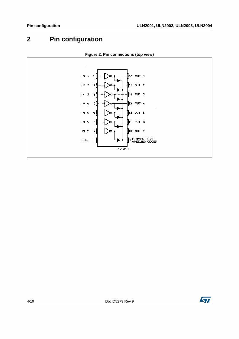
6 Typical performance characteristics
Figure 11. Collector current vs. saturation voltage (TJ = 25 °C)
Figure 12. Collector current vs. saturation voltage
I OU
T [m
A]
85°C25°C
-30°C
VCESAT [V]
IIN = 500 µA
Figure 13. Input current vs. input voltage Figure 14. Input current vs. input voltage(Ta = 25 °C)
ULN2003A
Typ
Max
Min
ULN2003ATa = 25°C Iout=100mA
Iout=200mA
Iout=300mA
Figure 15. Collector current vs. input current Figure 16. hFE vs. output current
IIN [μA]
I OU
T [m
A]
-30°C85°C
25°C
VCE = 2 V
1
10
100
1000
10000
1 10 100 1000
DC
Cur
rent
Tra
nsfe
r R
atio
(hF
E)
Output current IOUT [mA]
85 °C
-40 °C
25 °C
VCE = 2 V

Typical performance characteristics ULN2001, ULN2002, ULN2003, ULN2004
10/19 DocID5279 Rev 9
Figure 17. Peak collector current vs. duty cycle (DIP-16)
Figure 18. Peak collector current vs. duty cycle (SO-16)
0 20 40 60 80 DC0
100
200
300
400
500
Ic peak(mA)
Tamb=70°C(DIP16)
7 6 5 4 3 2
NUMBER OF ACTIVE OUTPUT
D96IN451
0 20 40 60 80 100 DC0
100
200
300
400
500
Ic peak(mA)
D96IN452A
7
5
3
2
NUMBER OF ACTIVE OUTPUT
Tamb=70°C(SO16)
DocID5279 Rev 9 11/19
ULN2001, ULN2002, ULN2003, ULN2004 Package information
19
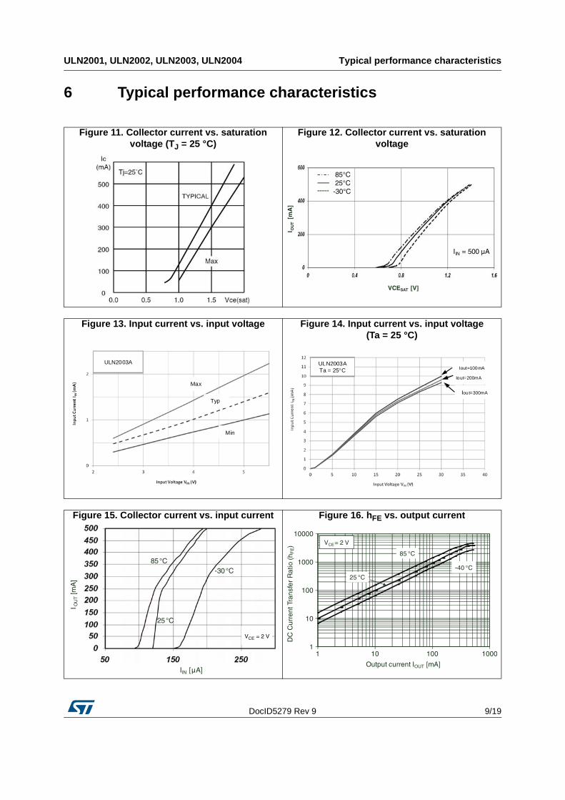
7 Package information
In order to meet environmental requirements, ST offers these devices in different grades of ECOPACK® packages, depending on their level of environmental compliance. ECOPACK® specifications, grade definitions and product status are available at: www.st.com. ECOPACK® is an ST trademark.
7.1 DIP-16L package information
Figure 19. DIP-16L package outline
0015895_E

Package information ULN2001, ULN2002, ULN2003, ULN2004
12/19 DocID5279 Rev 9
Table 4. DIP-16L mechanical data
Dim.mm.
Min. Typ. Max.
A 5.33
A1 0.38
A2 2.92 3.30 4.95
b 0.36 0.46 0.56
b2 1.14 1.52 1.78
c 0.20 0.25 0.36
D 18067 19.18 19.69
E 7.62 7.87 8.26
E1 6.10 6.35 7.11
e 2.54
e1 17.78
eA 7.62
eB 10.92
L 2.92 3.30 3.81

DocID5279 Rev 9 13/19
ULN2001, ULN2002, ULN2003, ULN2004 Package information
19
7.2 Plastic DIP-16L package information
Figure 20. Plastic DIP-16L package outline
Package information ULN2001, ULN2002, ULN2003, ULN2004
14/19 DocID5279 Rev 9
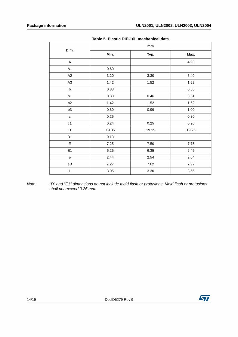
Note: “D” and “E1” dimensions do not include mold flash or protusions. Mold flash or protusions shall not exceed 0.25 mm.
Table 5. Plastic DIP-16L mechanical data
Dim. mm
Min. Typ. Max.
A 4.90
A1 0.60
A2 3.20 3.30 3.40
A3 1.42 1.52 1.62
b 0.38 0.55
b1 0.38 0.46 0.51
b2 1.42 1.52 1.62
b3 0.89 0.99 1.09
c 0.25 0.30
c1 0.24 0.25 0.26
D 19.05 19.15 19.25
D1 0.13
E 7.25 7.50 7.75
E1 6.25 6.35 6.45
e 2.44 2.54 2.64
eB 7.27 7.62 7.97
L 3.05 3.30 3.55
DocID5279 Rev 9 15/19
ULN2001, ULN2002, ULN2003, ULN2004 Package information
19
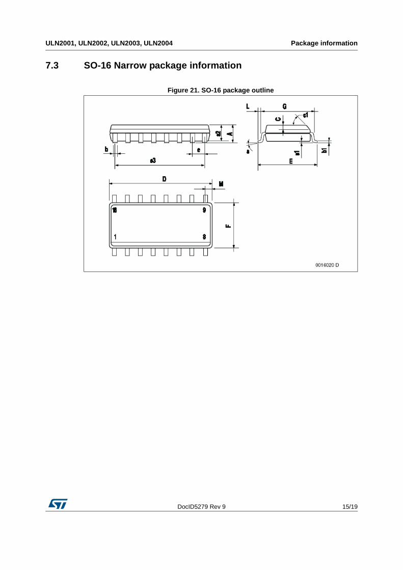
7.3 SO-16 Narrow package information
Figure 21. SO-16 package outline

Package information ULN2001, ULN2002, ULN2003, ULN2004
16/19 DocID5279 Rev 9
Table 6. SO-16 Narrow mechanical data
Dim.mm. inch.
Min. Typ. Max. Min. Typ. Max.
A 1.75 0.069
a1 0.1 0.25 0.004 0.009
a2 1.6 0.063
b 0.35 0.46 0.014 0.018
b1 0.19 0.25 0.007 0.010
C 0.5 0.020
c1 45° (typ.)
D(1) 9.8 10 0.386 0.394
E 5.8 6.2 0.228 0.244
e 1.27 0.050
e3 8.89 0.350
F(1) 3.8 4.0 0.150 0.157
G 4.60 5.30 0.181 0.208
L 0.4 1.27 0.150 0.050
M 0.62 0.024
S 8° (max.)

DocID5279 Rev 9 17/19
ULN2001, ULN2002, ULN2003, ULN2004 Order code
19
8 Order code
Table 7. Order code
Part number Package
ULN2001A DIP-16
ULN2002A DIP-16
ULN2003A DIP-16
ULN2004A DIP-16
ULN2003AA Plastic DIP-16L
ULN2001D1013TR SO-16 in tape and reel
ULN2002D1013TR SO-16 in tape and reel
ULN2003D1013TR SO-16 in tape and reel
ULN2004D1013TR SO-16 in tape and reel
Revision history ULN2001, ULN2002, ULN2003, ULN2004
18/19 DocID5279 Rev 9
9 Revision history
Table 8. Revision history
Date Revision Changes
05-Dec-2006 5 Order code updated and document reformatted.
28-Aug-2007 6 Added Table 1 in cover page.
07-May-2012 7Modified: Figure 12 on page 9.Added: Figure 13, 14, 15 and Figure 16 on page 9.
01-Jun-2012 8Updated: DIP-16L package mechanical data Table 4 on page 12 and Figure 19 on page 11.
22-Jul-2015 9
Added Plastic DIP16-L package.
Removed Device summary table.Updated Table 7: Order code.Added Section 7.2: Plastic DIP-16L package information.
Minor text changes.

DocID5279 Rev 9 19/19
ULN2001, ULN2002, ULN2003, ULN2004
19
IMPORTANT NOTICE – PLEASE READ CAREFULLY
STMicroelectronics NV and its subsidiaries (“ST”) reserve the right to make changes, corrections, enhancements, modifications, and improvements to ST products and/or to this document at any time without notice. Purchasers should obtain the latest relevant information on ST products before placing orders. ST products are sold pursuant to ST’s terms and conditions of sale in place at the time of order acknowledgement.
Purchasers are solely responsible for the choice, selection, and use of ST products and ST assumes no liability for application assistance or the design of Purchasers’ products.
No license, express or implied, to any intellectual property right is granted by ST herein.
Resale of ST products with provisions different from the information set forth herein shall void any warranty granted by ST for such product.
ST and the ST logo are trademarks of ST. All other product or service names are the property of their respective owners.
Information in this document supersedes and replaces information previously supplied in any prior versions of this document.
© 2015 STMicroelectronics – All rights reserved