Embed Size (px)
Citation preview
SFPCI - VME SERIES User’s Manual and Installation Guide
Solflower Computer, Inc3511 Thomas Road, Ste-2
Santa Clara, CA 95054(408) 982-8680, Fax (408) 982-8685
http://www.solflower.com
olflowerComputer, Inc.
SFPCI-VME SERIES User’s Manual and Installation Guide rev 2.0
2
Credit and Trademarks
SFPCI-VME, SF_PCI, SF_VME, PVME and PCI-VME are trademarks of Solflower Computer, Inc.
SPARC, SPARCstation, SPARCengine, SunOS, Solaris are registered trademarks of SPARC International, Inc. licensed exclusively to Sun Microsystems, Inc.
Universe is a registered trademark of Tundra Semiconductor Corporation.
This equipment generates, uses and can radiate radio frequency energy and if not installed and used in accordance with the Instruction Manual, may cause interference in radio communications.
Operation of this equipment in a residential area is likely to cause interference in which case the user at his own expense will be required to take whatever measures may be required to correct the interference.
This document presents information for users of Solflower Computer, Inc.’s SFPCI-VME Series of PCI-to-VME adapters.
Although the information contained within this document is considered accurate and characteristic of the subject product, Solflower Computer, Inc. reserves the right to make changes to this document and any product described herein to improve reliability, function or design. Solflower Computer, Inc. does not assume any liability arising out of the application or use of any product or circuit described herein.
No part of this document may be copied or reproduced in any form or by any means without the prior written consent of Solflower Computer, Inc.
Copyright 1997-2006, Solflower Computer, Inc.
SFPCI-VME SERIES User’s Guide and Installation Manual rev 2.0
Overview
CHAPTER 1 Overview
1.1 INTRODUCTION
The SFPCI-VME series of products provide a PCI-to-VMEbus interface, and the capability of handling PCI master and slave functions. In addition, the series provide VMEbus arbiter function, built-in DMA engine on board, as well as other system controller functions of the VMEbus as described in the following sections.
The major components of the SFPCI-VME product come in two categories:
• The hardware component is made up of a PCI interface, a VMEbus interface, a flat cable, and optional VME card cage including power supply and back-plane for integrating the VME boards.
• The software component is an optional driver that is installed in the Solaris 2.x. It enables users to retain their existing VMEbus drivers and transparently migrate their present VMEbus subsystem to a PCI-Based SPARC platform.
1.2 APPLICABLE DOCUMENTS
PCI Specification, Revision 2.1
VMEbus Specification Manual, Revision D IEEE STD 1014-9187
1.3 GENERAL DESCRIPTION
The SFPCI-VME series is a PCI-to-VMEbus adapter allowing master and slave accesses between these two host busses. In addition, VMEbus masters and slaves may carry out information transfer with each other without stepping on the PCI bus.
A VMEbus master to PCI slave access takes place in a specified 1 MB “window,” via a mapping register. A24 and A32 VMEbus accesses are also supported.
The PCI bus master to VMEbus slave addressing is accomplished in accordance with the PCI addressing scheme. Internal mapping registers inside the SFPCI-VME series are used to access the entire 4 GB of PCI bus address space. SFPCI-VME can transfer data from/to VME bus upto 60-70Mb/sec, and supports the following address and data transfer modes.
- A32/A24/A16 Master and Slave- D64 (MBLT)/D32/D16/D08 Master and Slave- BLT, ADOH, RMW, LOCK
rev 2.0 SFPCI-VME SERIES User’s Guide and Installation Manual 3
Overview
1.4 UNPACKING INSTRUCTIONS
Perform a visual inspection of the shipping carton for any handling damage. If any shipping carton is severely damaged, open the carton box with the carrier agent’s presence. Carefully remove the contents and ensure that all the pieces are there. The printed circuit boards are wrapped in electrostatic-safe bags. We recommend that you save the shipping carton and the packing material for future use, in case the product must be reshipped or returned to Solflower.
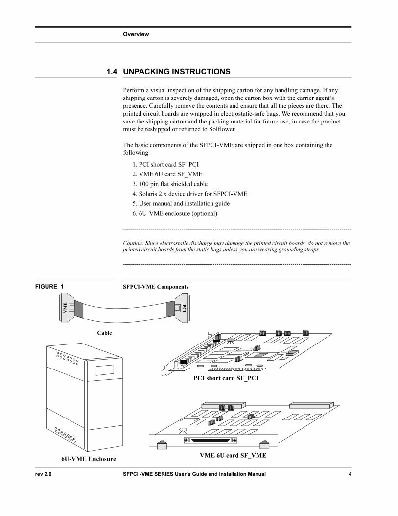
The basic components of the SFPCI-VME are shipped in one box containing the following
1. PCI short card SF_PCI2. VME 6U card SF_VME3. 100 pin flat shielded cable4. Solaris 2.x device driver for SFPCI-VME5. User manual and installation guide6. 6U-VME enclosure (optional)
---------------------------------------------------------------------------------------------------------------------
Caution: Since electrostatic discharge may damage the printed circuit boards, do not remove the printed circuit boards from the static bags unless you are wearing grounding straps.
---------------------------------------------------------------------------------------------------------------------
FIGURE 1 SFPCI-VME Components
6U-VME Enclosure VME 6U card SF_VME
PCI short card SF_PCI
Cable
VM
E PCI
rev 2.0 SFPCI -VME SERIES User’s Guide and Installation Manual 4
SFPCI-VME Series Installation
CHAPTER 2 SFPCI-VME Series Installation
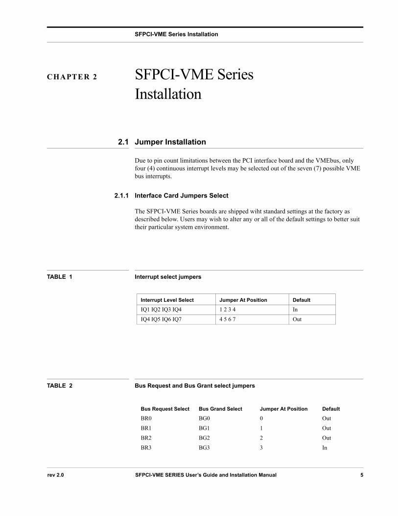
2.1 Jumper Installation
Due to pin count limitations between the PCI interface board and the VMEbus, only four (4) continuous interrupt levels may be selected out of the seven (7) possible VME bus interrupts.
2.1.1 Interface Card Jumpers Select
The SFPCI-VME Series boards are shipped wiht standard settings at the factory as described below. Users may wish to alter any or all of the default settings to better suit their particular system environment.
TABLE 1 Interrupt select jumpers
Interrupt Level Select Jumper At Position Default
IQ1 IQ2 IQ3 IQ4 1 2 3 4 In
IQ4 IQ5 IQ6 IQ7 4 5 6 7 Out
TABLE 2 Bus Request and Bus Grant select jumpers
Bus Request Select Bus Grand Select Jumper At Position Default
BR0 BG0 0 Out
BR1 BG1 1 Out
BR2 BG2 2 Out
BR3 BG3 3 In
rev 2.0 SFPCI-VME SERIES User’s Guide and Installation Manual 5
SFPCI-VME Series Installation
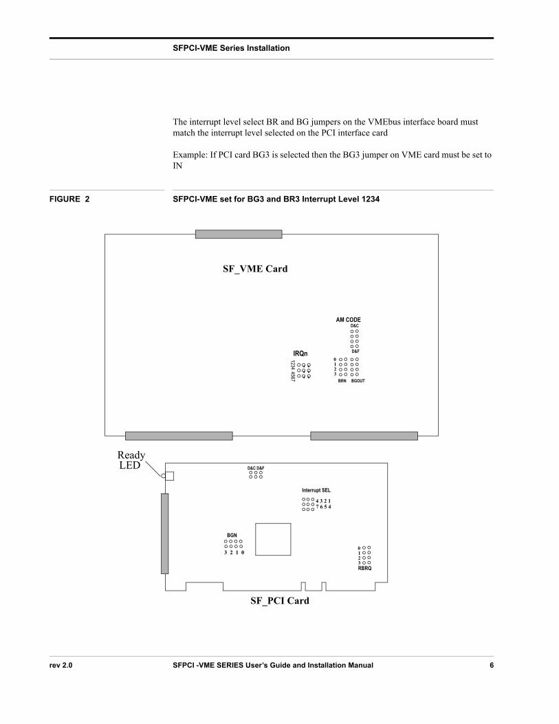
The interrupt level select BR and BG jumpers on the VMEbus interface board must match the interrupt level selected on the PCI interface card
Example: If PCI card BG3 is selected then the BG3 jumper on VME card must be set to IN
FIGURE 2 SFPCI-VME set for BG3 and BR3 Interrupt Level 1234
3210
BGOUTBRN
D&C
D&F
AM CODE
12344567
IRQn
3210
3 2 1 0
RBRQ
BGN
SF_PCI Card
ReadyLED
4 3 2 17 6 5 4
Interrupt SEL
D&C D&F
SF_VME Card
rev 2.0 SFPCI -VME SERIES User’s Guide and Installation Manual 6
SFPCI-VME Series Installation
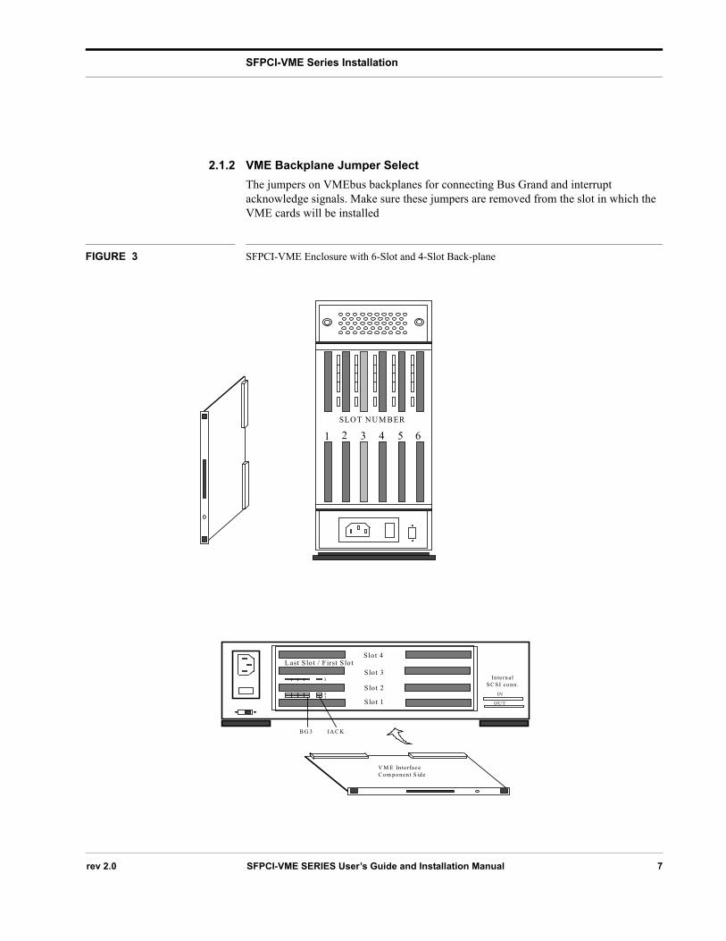
2.1.2 VME Backplane Jumper SelectThe jumpers on VMEbus backplanes for connecting Bus Grand and interrupt acknowledge signals. Make sure these jumpers are removed from the slot in which the VME cards will be installed
FIGURE 3 SFPCI-VME Enclosure with 6-Slot and 4-Slot Back-plane
1 2 3 4 5 6SLOT NUM BER
Slot 4
Slot 3
Slot 2
Slot 1
L ast S lot / F irst S lot
In terna lSC SI conn .
IN
O U T12
3
B G 3 IA C K
V M E In terfaceC om ponen t S ide
rev 2.0 SFPCI-VME SERIES User’s Guide and Installation Manual 7
SFPCI-VME Series Installation
2.2 SF_PCI Card Installation
Before you start with the installation, you may refer to system owner’s guide for the instruction how to install PCI card to Sun system. The Sun doc is online and available at the web site www.sun.com
Follow these instructions:
- Power off the system. - Remove the side access cover. - Attach the wrist strap.
---------------------------------------------------------------------------------------------------------------------
Caution - Use proper ESD grounding techniques when handling components. Wear an antistatic wrist strap and use an ESD-protected mat. Store ESD-sensitive components in antistatic bags before placing them on any surface.
---------------------------------------------------------------------------------------------------------------------- Install the PCI card as follows
a. Position the PCI card into the chassis. b. Lower the PCI card connector so that it touches its associated PCI card slot on the motherboard.c. Guide the PCI card back panel into the chassis backpanel. d. At the two upper corners of the card, push the card straight downward into the slot until the card is fully seated. e. Using a Phillips-head screwdriver, replace the screw securing the card bracket tab to the system chassis. Replace the side access cover.
2.2.1 Install SF_PCI Card to Sun Microelectronics (SME) Ultra AX SPARCengine
The Ultra AX SPARCengine provides 4 PCI slots. The two 64 bit connectors are PCI bus A and the other two, hardwired with internal devices are PCI bus B. You can install PCI short card to any available PCI slot, but for best performance, the PCI short card should be installed in 64bit PCI slot (PCI bus A).
rev 2.0 SFPCI -VME SERIES User’s Guide and Installation Manual 8
SFPCI-VME Series Installation
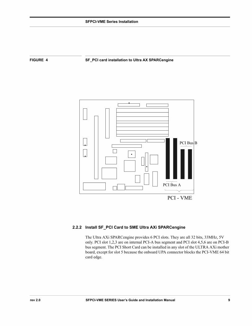
FIGURE 4 SF_PCI card installation to Ultra AX SPARCengine
2.2.2 Install SF_PCI Card to SME Ultra AXi SPARCengine
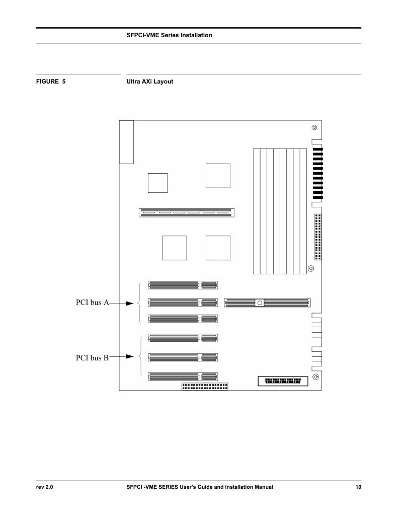
The Ultra AXi SPARCengine provides 6 PCI slots. They are all 32 bits, 33MHz, 5V only. PCI slot 1,2,3 are on internal PCI-A bus segment and PCI slot 4,5,6 are on PCI-B bus segment. The PCI Short Card can be installed in any slot of the ULTRA AXi mother board, except for slot 5 because the onboard UPA connector blocks the PCI-VME 64 bit card edge.
PCI Bus B
PCI Bus A
PCI - VME
rev 2.0 SFPCI-VME SERIES User’s Guide and Installation Manual 9
SFPCI-VME Series Installation
FIGURE 5 Ultra AXi Layout
PCI bus A
PCI bus B
rev 2.0 SFPCI -VME SERIES User’s Guide and Installation Manual 10
SFPCI-VME Series Installation
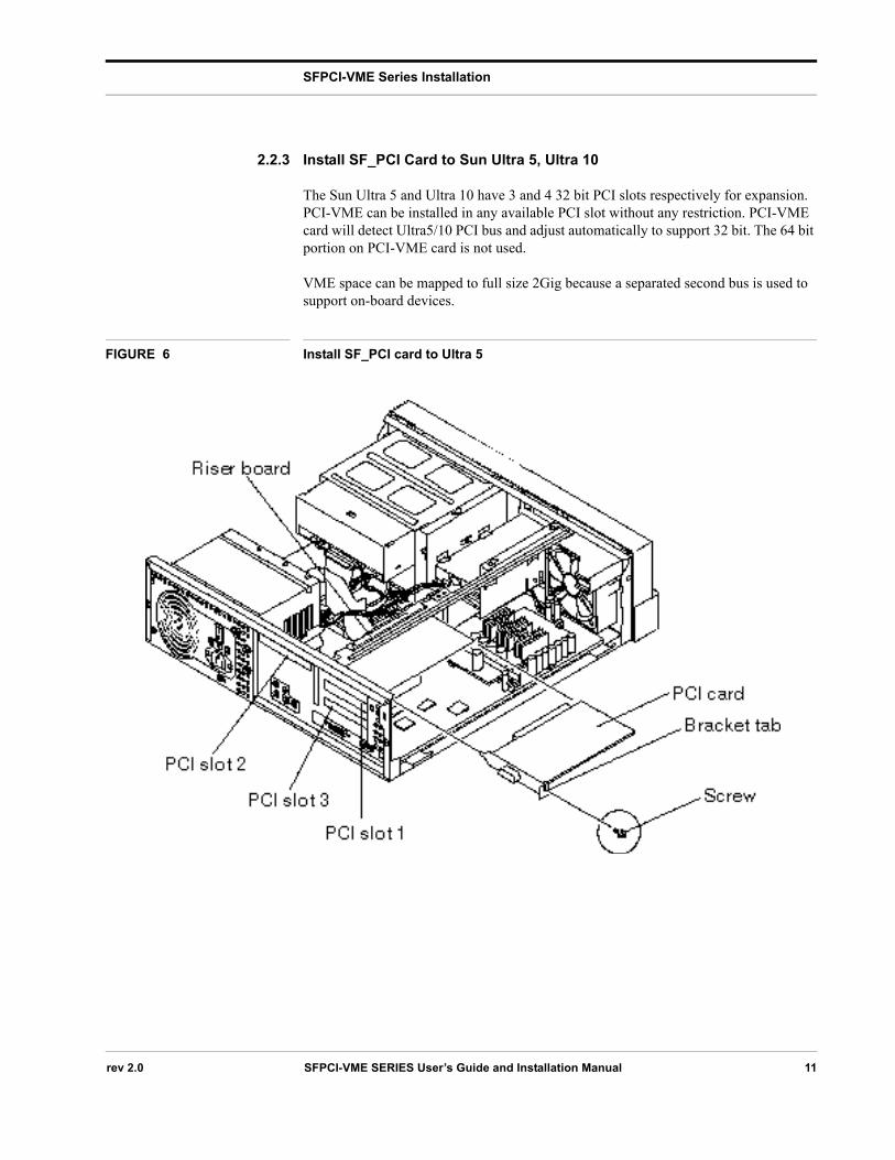
2.2.3 Install SF_PCI Card to Sun Ultra 5, Ultra 10
The Sun Ultra 5 and Ultra 10 have 3 and 4 32 bit PCI slots respectively for expansion. PCI-VME can be installed in any available PCI slot without any restriction. PCI-VME card will detect Ultra5/10 PCI bus and adjust automatically to support 32 bit. The 64 bit portion on PCI-VME card is not used.
VME space can be mapped to full size 2Gig because a separated second bus is used to support on-board devices.
FIGURE 6 Install SF_PCI card to Ultra 5
rev 2.0 SFPCI-VME SERIES User’s Guide and Installation Manual 11
SFPCI-VME Series Installation
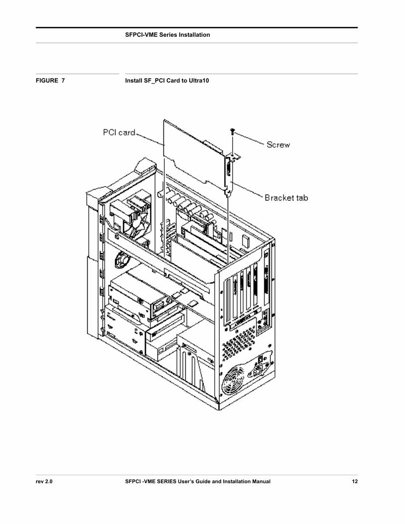
FIGURE 7 Install SF_PCI Card to Ultra10
rev 2.0 SFPCI -VME SERIES User’s Guide and Installation Manual 12
SFPCI-VME Series Installation
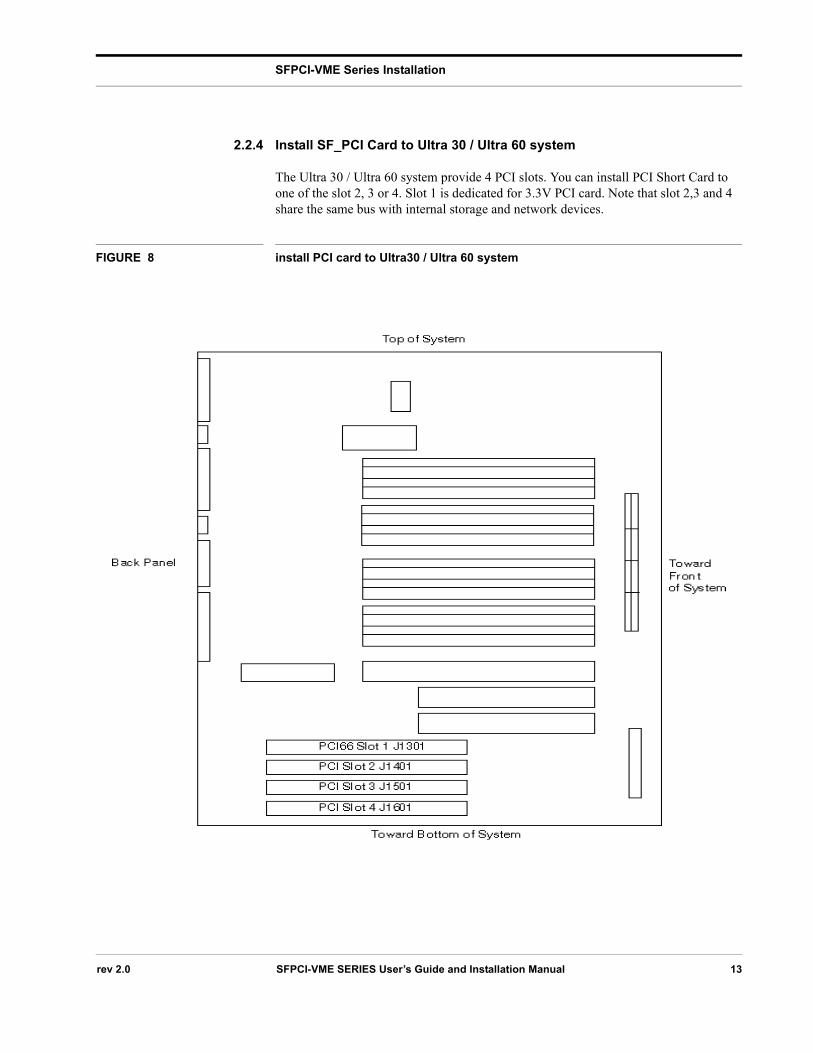
2.2.4 Install SF_PCI Card to Ultra 30 / Ultra 60 system
The Ultra 30 / Ultra 60 system provide 4 PCI slots. You can install PCI Short Card to one of the slot 2, 3 or 4. Slot 1 is dedicated for 3.3V PCI card. Note that slot 2,3 and 4 share the same bus with internal storage and network devices.
FIGURE 8 install PCI card to Ultra30 / Ultra 60 system
rev 2.0 SFPCI-VME SERIES User’s Guide and Installation Manual 13
SFPCI-VME Series Installation
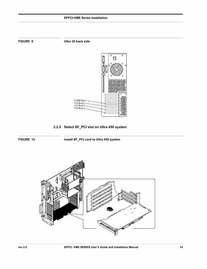
FIGURE 9 Ultra 30 back side
2.2.5 Select SF_PCI slot on Ultra 450 system
FIGURE 10 install SF_PCI card to Ultra 450 system
rev 2.0 SFPCI -VME SERIES User’s Guide and Installation Manual 14
SFPCI-VME Series Installation
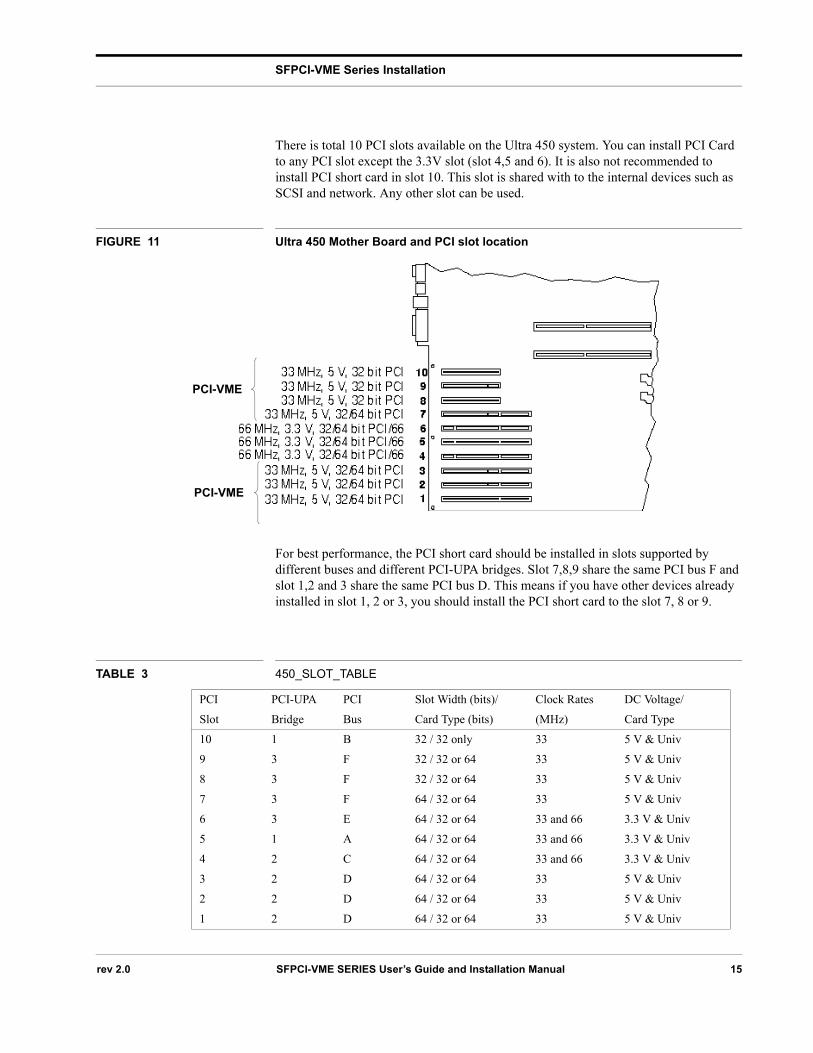
There is total 10 PCI slots available on the Ultra 450 system. You can install PCI Card to any PCI slot except the 3.3V slot (slot 4,5 and 6). It is also not recommended to install PCI short card in slot 10. This slot is shared with to the internal devices such as SCSI and network. Any other slot can be used.
FIGURE 11 Ultra 450 Mother Board and PCI slot location
For best performance, the PCI short card should be installed in slots supported by different buses and different PCI-UPA bridges. Slot 7,8,9 share the same PCI bus F and slot 1,2 and 3 share the same PCI bus D. This means if you have other devices already installed in slot 1, 2 or 3, you should install the PCI short card to the slot 7, 8 or 9.
TABLE 3 450_SLOT_TABLE
PCI
Slot
PCI-UPA
Bridge
PCI
Bus
Slot Width (bits)/
Card Type (bits)
Clock Rates
(MHz)
DC Voltage/
Card Type
10 1 B 32 / 32 only 33 5 V & Univ
9 3 F 32 / 32 or 64 33 5 V & Univ
8 3 F 32 / 32 or 64 33 5 V & Univ
7 3 F 64 / 32 or 64 33 5 V & Univ
6 3 E 64 / 32 or 64 33 and 66 3.3 V & Univ
5 1 A 64 / 32 or 64 33 and 66 3.3 V & Univ
4 2 C 64 / 32 or 64 33 and 66 3.3 V & Univ
3 2 D 64 / 32 or 64 33 5 V & Univ
2 2 D 64 / 32 or 64 33 5 V & Univ
1 2 D 64 / 32 or 64 33 5 V & Univ
PCI-VME
PCI-VME
rev 2.0 SFPCI-VME SERIES User’s Guide and Installation Manual 15
SFPCI-VME Series Installation
2.2.6 SF_PCI Installation on SunFireV250There are 6 PCI slots on a Sun Fire V250. Any 5volt PCI slot (PCI4, 1, and 0) is OK to install the SF_PCI card, as they are in the same PCI segment. All other PCI slots are 3.3V slots and are not suitable for SFPCI-VME. The following are sample installations.
PCI0: SF_PCI
PCI1: other, such as a SCSI controller
PCI2:
PCI3:
PCI4:
PCI5: XVR-100 graphic card
or
PCI0:
PCI1: other, such as a SCSI controller
PCI2:
PCI3:
PCI4: SF_PCI
PCI5: XVR-100 graphic card
TABLE 4 V250 PCI slots
PCI
Slot Bridge
PCI
Bus
Slot Width (bits)/
Card Type (bits)
Clock Rates
(MHz)
DC Voltage/
Card Type
5 JIO1 2b 64 / 32 or 64 33 and 66 3.3 V
4 JIO1 2a 64 / 32 or 64 33 5 V
3 JIO0 1a 64 / 32 or 64 33 and 66 3.3 V
2 JIO0 1b 64 / 32 or 64 33 and 66 3.3 V
1 JIO1 2a 64 / 32 or 64 33 5 V
0 JIO1 2a 64 / 32 or 64 33 5 V
rev 2.0 SFPCI -VME SERIES User’s Guide and Installation Manual 16
SFPCI-VME Series Installation
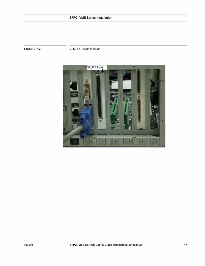
FIGURE 12 V250 PCI slots location
rev 2.0 SFPCI-VME SERIES User’s Guide and Installation Manual 17
SFPCI-VME Series Installation
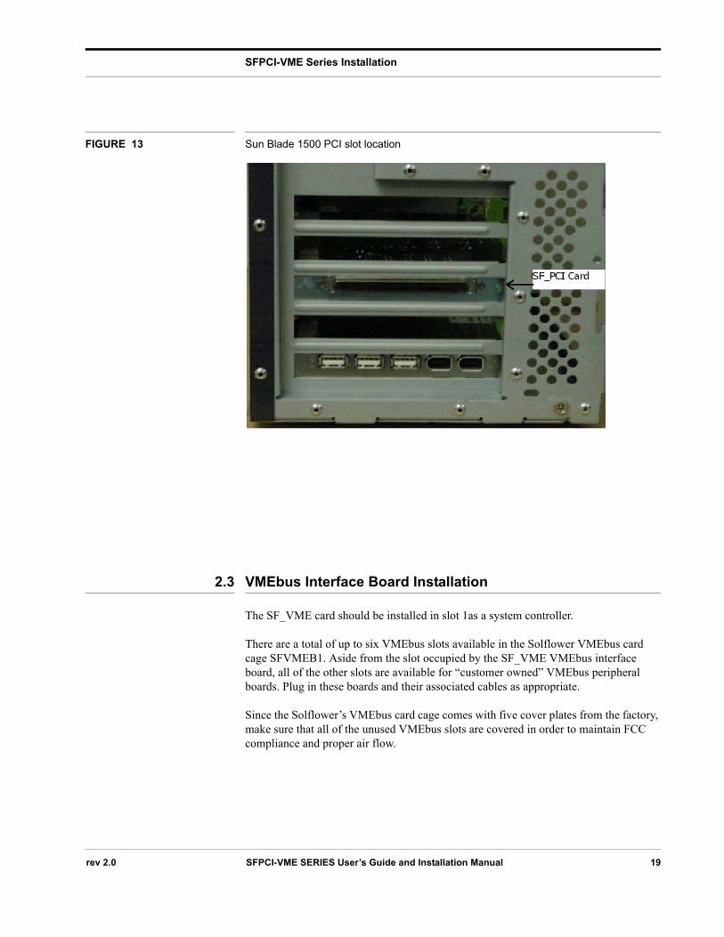
2.2.7 SF_PCI card Installation on Sun Blade 1500There are two bus segment for total of five PCI slots. PCI0, PCI1, PCI2, and PCI3 are under one PCI segment while PCI4 is under another.
Slot 0 might be occupied by pre installed FireWire and USB card. This will leave a total of 4 PCI slots available. And if one of the 4 PCI slot is used to install a graphic card such as a XVR-100, this will further reduce the available PCI slots to 3. The following scheme is an example of PCI slot assignment, and had been tested for SF_PCI cards.
PCI 0: FireWire USB card
PCI1:
PCI2: SF_PCI card
PCI3:
PCI4: XVR-100 Graphic card
In fact, with FireWire USB card at PCI0 and XVR-100 at PCI4, any one of the remaining PCI slots (PCI1, 2, 3) can be installed with SFPCI, and tested to work.
TABLE 5 Sun Blade 1500 PCI slots
PCI
Slot
Slot Width (bits)/
Card Type (bits)
Clock Rates
(MHz)
DC Voltage/
Card Type
4 64 / 32 33 and 66 3.3 V
3 64 / 32 33 5 V
2 64 / 32 33 5 V
1 32 33 5 V
0 32 33 5 V
rev 2.0 SFPCI -VME SERIES User’s Guide and Installation Manual 18
SFPCI-VME Series Installation
FIGURE 13 Sun Blade 1500 PCI slot location
2.3 VMEbus Interface Board Installation
The SF_VME card should be installed in slot 1as a system controller.
There are a total of up to six VMEbus slots available in the Solflower VMEbus card cage SFVMEB1. Aside from the slot occupied by the SF_VME VMEbus interface board, all of the other slots are available for “customer owned” VMEbus peripheral boards. Plug in these boards and their associated cables as appropriate.
Since the Solflower’s VMEbus card cage comes with five cover plates from the factory, make sure that all of the unused VMEbus slots are covered in order to maintain FCC compliance and proper air flow.
rev 2.0 SFPCI-VME SERIES User’s Guide and Installation Manual 19
SFPCI-VME Series Installation
2.4 Cable Installation
Check the pins of the connector on both sides for broken or bent pins. If all pins are not bent or damaged, position the Solflower SF_VME card cage adjacent to the SPARC system, and install the cable between the PCIbus interface board and the VMEbus interface board. Make sure that the connectors are locked
The cable is marked as to VME and to PCIbus and should not be resversed. Note: If the cable from PCI to VME is correctly connected and the power of VME box is on, the green LED on PCI card is on for ready
2.5 Boot Up System
After the system is powered up and rebooted, Solaris will probe all installed PCI devices and display the attached device configuration
Now go to section Software Installation Chapter 5 for install Solflower’s pvme device driver.
rev 2.0 SFPCI -VME SERIES User’s Guide and Installation Manual 20
Architecture Description
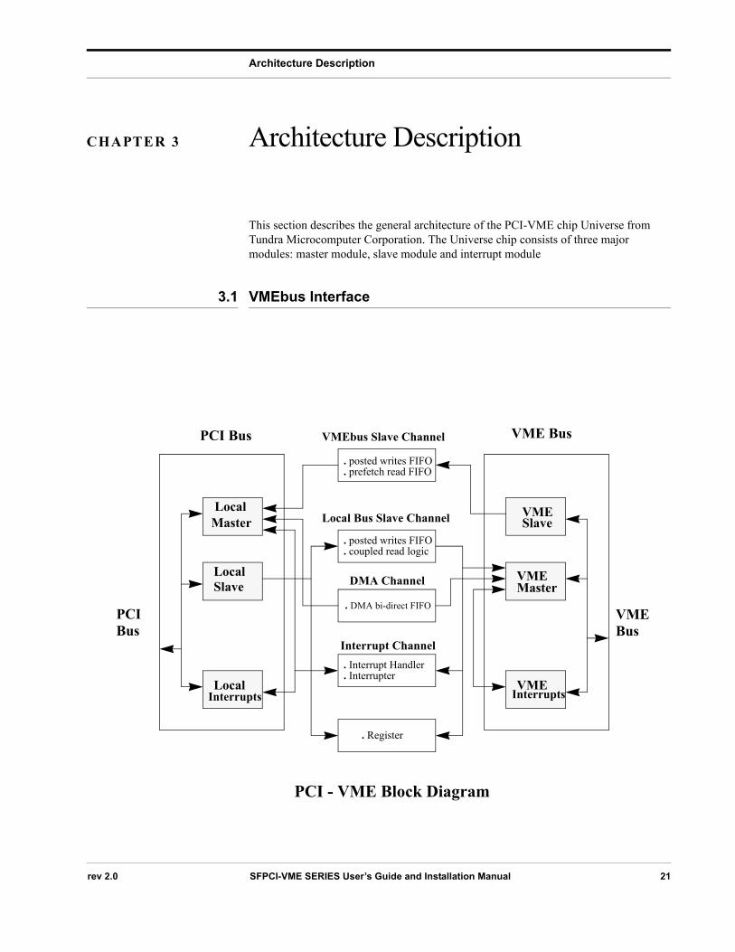
CHAPTER 3 Architecture Description
This section describes the general architecture of the PCI-VME chip Universe from Tundra Microcomputer Corporation. The Universe chip consists of three major modules: master module, slave module and interrupt module
3.1 VMEbus Interface
PCI Bus VME Bus
VMESlave
VMEMaster
VMEInterrupts
VME
LocalMaster
SlaveLocal
LocalInterrupts
VMEbus Slave Channel
. posted writes FIFO
. prefetch read FIFO
. coupled read logic
. posted writes FIFO
Local Bus Slave Channel
DMA Channel
Interrupt Channel
. DMA bi-direct FIFO
. Interrupt Handler
. Interrupter
. Register
PCI
PCI - VME Block Diagram
Bus Bus
rev 2.0 SFPCI-VME SERIES User’s Guide and Installation Manual 21
Architecture Description
3.1.1 Universe as VMEbus SlaveThe Universe VME Slave Channel accepts all of the addressing and data transfer modes documented in the VME64 specification (except A64 and those intended to support 3U applications, i.e. A40 and MD32). Incoming write transactions from the VMEbus may be treated as either coupled posted, depending upon the programing of the VMEbus slave image. With posted write transactions, data is written to a Posted Write Receive FIFO (RXFIFO), and the VMEbus master receives data acknowledgment from the Universe. Write data is transferred to the PCI resource from the RXFIFO without the involvement of the initiating VMEbus master. With a coupled cycle, the VMEbus master only receives data acknowledgment when the transaction is complete on the PCI bus. This means that the VMEbus is unavailable to other masters while the PCI bus transaction is executed.
Read transactions may be either prefetched or coupled. If enabled by the users, a prefetched read is initiated when VMEbus master requests a block read transaction (BLT or MBLT) and this mode is enabled. When the Universe receives the block read request, it begins to fill its Read Data FIFO (RDFIFO) using burst transactions from the PCI resource. The initiating VMEbus master then acquires its block read data from the RD FIFO rather than from the PCI resources directly
3.1.2 Universe as VMEbus MasterThe Universe becomes VMEbus master when the VME Master Interface is internally requested by the PCI Bus Slave Channel, the DMA Channel, or the Interrupt Channel. The Interrupt Channel always has priority over the other two channels. Several mechanisms are available to configure the relative priority that the PCI Bus Slave Channel and DMA Channel have over ownership of the VMEbus Master Interface.
The Universe’s VME Master Interface generates all of the addressing and data transfer modes documented in the VME64 specification (except A64 and those intended to support 3U applications, i.e. A40 and MD32). The Universe is also compatible with all VMEbus modules conforming to pre-VME64 specifications. As VMEbus master, the Universe supports Read-Modify-Write (RMW), and Address-Only-with-Handshake (ADOH) but does not accept RETRY* as a termination from the VMEbus slave. The ADOH cycle is used to implement the VMEbus Lock command allowing a PCI master to lock VME resources.
3.2 PCI Bus Interface
3.2.1 Universe as PCI Slave
Read transactions from the PCI bus are always processed as coupled. Write transactions may be either coupled or posted, depending upon the setting of the PCI bus slave image. With a posted write transaction, write data is written to a Posted Write Transmit FIFO (TXFIFO) and the PCI bus master receives data acknowledgment from the Universe with zero wait states. Meanwhile, the Universe obtains the VMEbus and writes the data to the VMEbus resource independent of the initiating PCI master.
rev 2.0 SFPCI -VME SERIES User’s Guide and Installation Manual 22
Architecture Description
To allow PCI masters to perform RMW and ADOH cycles, the Universe provides a Special Cycle Generator. The Special Cycle Generator can be used in combination with a VMEbus ownership function to guarantee PCI masters exclusive access to VMEbus resources over several VMEbus transactions.
3.2.2 Universe as PCI Master
The Universe becomes PCI master when the PCI Master Interface is internally requested by the VME Slave Channel or the DMA Channel. There are mechanisms provided which allow the user to configure the relative priority of the VME Slave Channel and the DMA Channel.
3.3 Interrupter and Interrupt Handler
3.3.1 Interrupter
The Universe interrupt channel provides a flexible scheme to map interrupts to either the PCI bus or VMEbus interface. Interrupts are generated from either hardware or software sources. Interrupt sources can be mapped to any of the PCI bus or VMEbus interrupt output pins. Interrupt sources mapped to VMEbus interrupts are generated on the VMEbus interrupt output pins VIRQ# [7:1]. When a software and hardware source are assigned to the same VIRQn# pin, the software source always has higher priority.
Interrupt sources mapped to PCI bus interrupts are generated on one of the INT#[7:0] pins. To be fully PCI compliant, all interrupt sources must be routed to a single INT# pin.
For VMEbus interrupt outputs, the Universe interrupter supplies an 8-bit STATUS/ID to a VMEbus interrupt handler during the IACK cycle, and optionally generates an internal interrupt to signal that the interrupt vector has been provided.
Interrupts mapped to PCI bus outputs are serviced by the PCI interrupt controller. The CPU determines which interrupt sources are active by reading an interrupt status register in the Universe. The source negates its interrupt when it has been serviced by the CPU.
3.3.2 VMEbus Interrupt Handling
A VMEbus interrupt triggers the Universe to generate a normal VMEbus IACK cycle and generate the specified interrupt output. When the IACK cycle is complete, the Universe releases the VMEbus and the interrupt vector is read by the PCI resource servicing the interrupt output. Software interrupts are ROAK, while hardware, and internal interrupts are RORA.
rev 2.0 SFPCI-VME SERIES User’s Guide and Installation Manual 23
Architecture Description
3.4 DMA Controller
The Universe provides an internal DMA controller for high performance data transfer between the PCI and VMEbus. DMA operations between the source and destination bus are decoupled through the use of a single bidirectional FIFO (DMAFIFO). Parameters for the DMA transfer are software configurable in the Universe registers.
The principle mechanism for DMA transfers is the same for operations in either direction (PCI to VME, or VME to PCI), only the relative identity of the source and destination bus changes. In a DMA transfer, the Universe gains control of the source bus and reads data into its DMAFIFO. Following specific rules of DMAFIFO operation, it then acquires the destination bus and writes data from its DMAFIFO.
The DMA controller can be programmed to perform multiple blocks of transfers using entries in a linked-list. The DMA will work through the transfers in the linked-list following pointers at the end of each linked-list entry. Linked-list operation is initiated through a pointer in an internal Universe register, but the inked-list itself resides in PCI bus memory.
rev 2.0 SFPCI -VME SERIES User’s Guide and Installation Manual 24
Performance Consideration
CHAPTER 4 Performance Consideration
As a VME bus bridge, the Universe’s most important function is passing data. This function resides in three of its channels: the PCI Slave Channel, VME Slave Channel, and the DMA Channel. Since each channel operates independently of the others and because each has its own unique characteristics, the following analysis reviews the data transfer performance for each channel. Where relevant, descriptions of some of the factors affecting performance and how they might be tuned in different environments are discussed.
The decoupled nature of the Universe can cause some confusion in discussing performance parameters. This is because, in a fully decoupled bus bridge, the two opposing buses operate at their peak performance independent of the other. The Universe, however, because of the finite size of its FIFOs, can never represent a 100% decoupled bridge. As the FIFOs fill or empty (depending on the direction of data movement) the two buses tend to migrate to matched performance where the higher performing bus is forced to slow down to match the lower performing one. This limits the sustained performance of the device. Some factors such as the PCI Aligned Burst Size and VME request/release modes can limit the effect of the finite FIFO size and boost performance.
Another aspect in considering the performance of a device is bandwidth consumption. The greater bandwidth consumed to transfer a given amount of data, the less is available for the bus masters. Decoupling significantly improves the Universe’s bandwidth consumption, and on the PCI bus allows it to use the minimum permitted by the PCI specification.
To simplify the analysis and allow comparison with other devices, Universe performance has been calculated using the following assumptions:
As a PCI master: - one clock bus grant latency
- zero wait state PCI target
As a VME master: - ideal VME slave response (DS* to DTACK* = 30ns)
Assumed as part of any calculations on VME, performance is the inclusion of VME transceivers with propagation delay of 4 ns
rev 2.0 SFPCI-VME SERIES User’s Guide and Installation Manual 25
Performance Consideration
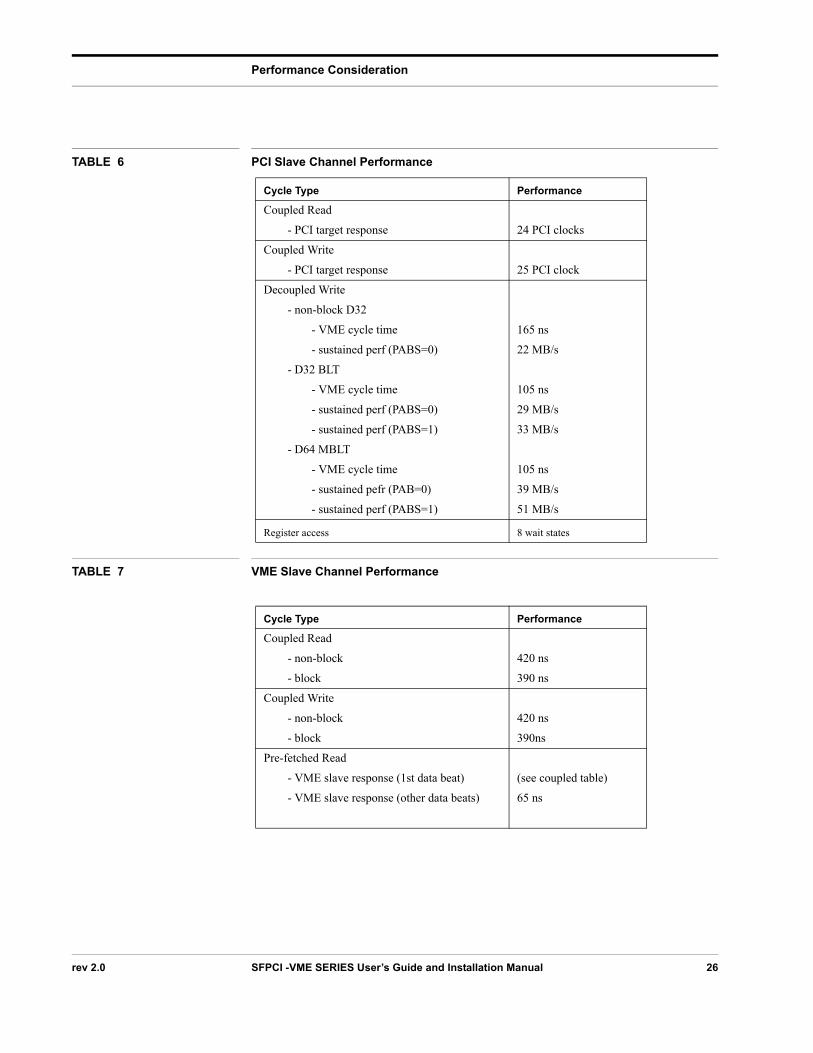
TABLE 6 PCI Slave Channel Performance
Cycle Type Performance
Coupled Read
- PCI target response 24 PCI clocks
Coupled Write
- PCI target response 25 PCI clock
Decoupled Write
- non-block D32
- VME cycle time
- sustained perf (PABS=0)
- D32 BLT
- VME cycle time
- sustained perf (PABS=0)
- sustained perf (PABS=1)
- D64 MBLT
- VME cycle time
- sustained pefr (PAB=0)
- sustained perf (PABS=1)
165 ns
22 MB/s
105 ns
29 MB/s
33 MB/s
105 ns
39 MB/s
51 MB/s
Register access 8 wait states
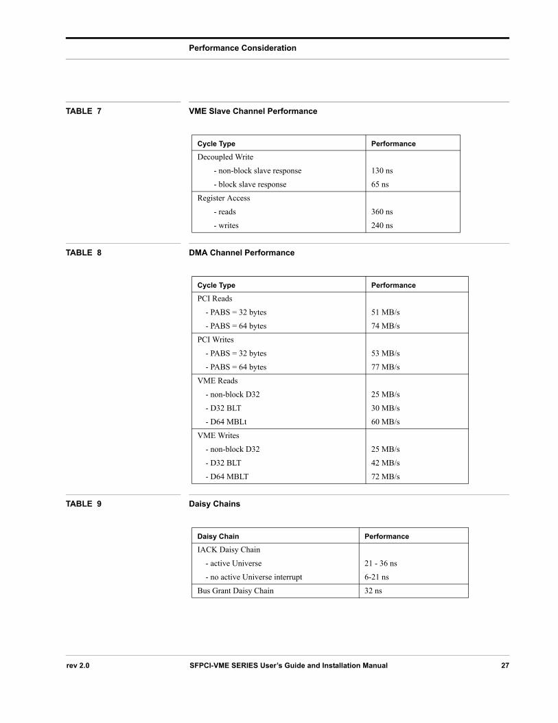
TABLE 7 VME Slave Channel Performance
Cycle Type Performance
Coupled Read
- non-block
- block
420 ns
390 ns
Coupled Write
- non-block
- block
420 ns
390ns
Pre-fetched Read
- VME slave response (1st data beat)
- VME slave response (other data beats)
(see coupled table)
65 ns
rev 2.0 SFPCI -VME SERIES User’s Guide and Installation Manual 26
Performance Consideration
Decoupled Write
- non-block slave response
- block slave response
130 ns
65 ns
Register Access
- reads
- writes
360 ns
240 ns
TABLE 8 DMA Channel Performance
Cycle Type Performance
PCI Reads
- PABS = 32 bytes
- PABS = 64 bytes
51 MB/s
74 MB/s
PCI Writes
- PABS = 32 bytes
- PABS = 64 bytes
53 MB/s
77 MB/s
VME Reads
- non-block D32
- D32 BLT
- D64 MBLt
25 MB/s
30 MB/s
60 MB/s
VME Writes
- non-block D32
- D32 BLT
- D64 MBLT
25 MB/s
42 MB/s
72 MB/s
TABLE 9 Daisy Chains
Daisy Chain Performance
IACK Daisy Chain
- active Universe
- no active Universe interrupt
21 - 36 ns
6-21 ns
Bus Grant Daisy Chain 32 ns
TABLE 7 VME Slave Channel Performance
Cycle Type Performance
rev 2.0 SFPCI-VME SERIES User’s Guide and Installation Manual 27
Performance Consideration
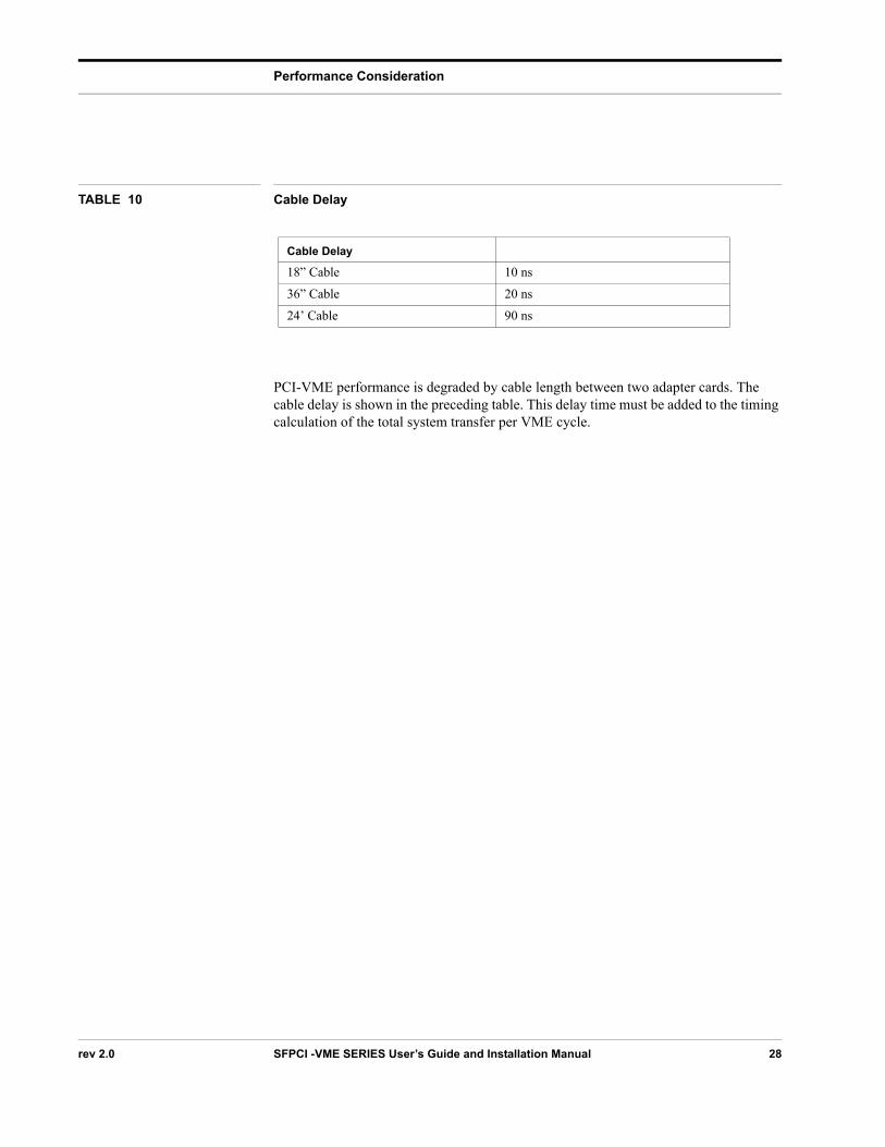
PCI-VME performance is degraded by cable length between two adapter cards. The cable delay is shown in the preceding table. This delay time must be added to the timing calculation of the total system transfer per VME cycle.
TABLE 10 Cable Delay
Cable Delay
18” Cable 10 ns
36” Cable 20 ns
24’ Cable 90 ns
rev 2.0 SFPCI -VME SERIES User’s Guide and Installation Manual 28
Software Installation
CHAPTER 5 Software Installation
5.1 Introduction
The Solflower PVME is PCI-to-VME bridge and nexus driver. It permits the installation, configuration, and use of VME devices on Sun Microsystems UltraSPARC platforms that support the PCI bus.
With the PVME bridge and nexus driver, most VME device drivers need only be written to conform to Sun’s DDI, and they should work transparently, with no need to be aware that they are communicating to Solaris through a bus bridge.
5.2 PVME Features
• Complete Solaris Nexus driver, providing leaf driver management and translation for VME device mappings, interrupts, and DMA.
• Direct VMEbus access, through the export of VME address space device files.• A special programmable DMA engine that transparently provides high-performance
DMA transfers to and from VME address spaces when the VME device files are accessed by read(2) and write(2) operations.
• VMEbus power-off detection and management for user processes that access the PVME device files directly.
• Selectable operation modes for VME block transfer, arbitration, and posted writes.• Loadable and unloadable Nexus driver.
The PVME release 1.2 from Solflower is comprised of the following components:
5.3 Components
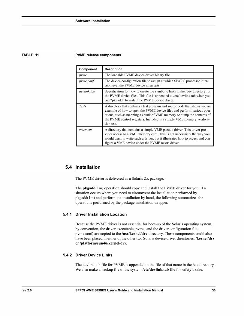
The PVME release from Solflower, in addition to the binary device driver itself, is comprised of components for driver configuration and for illustrating testing and usage. Table 8, “PVME release components,” lists and describes each component.
rev 2.0 SFPCI-VME SERIES User’s Guide and Installation Manual 29
Software Installation
5.4 Installation
The PVME driver is delivered as a Solaris 2.x package.
The pkgadd(1m) operation should copy and install the PVME driver for you. If a situation occurs where you need to circumvent the installation performed by pkgadd(1m) and perform the installation by hand, the following summarizes the operations performed by the package installation wrapper.
5.4.1 Driver Installation Location
Because the PVME driver is not essential for boot-up of the Solaris operating system, by convention, the driver executable, pvme, and the driver configuration file, pvme.conf, are copied to the /usr/kernel/drv directory. These components could also have been placed in either of the other two Solaris device driver directories: /kernel/drv or /platform/sun4u/kernel/drv.
5.4.2 Driver Device Links
The devlink.tab file for PVME is appended to the file of that name in the /etc directory. We also make a backup file of the system /etc/devlink.tab file for safety’s sake.
TABLE 11 PVME release components
Component Description
pvme The loadable PVME device driver binary file
pvme.conf The device configuration file to assign at which SPARC processor inter-rupt level the PVME device interrupts.
devlink.tab Specification for how to create the symbolic links in the /dev directory for the PVME device files. This file is appended to /etc/devlink.tab when you run “pkgadd” to install the PVME device driver.
Tests A directory that contains a test program and source code that shows you an example of how to open the PVME device files and perform various oper-ations, such as mapping a chunk of VME memory or dump the contents of the PVME control registers. Included is a simple VME memory verifica-tion test.
vmemem A directory that contains a simple VME pseudo driver. This driver pro-vides access to a VME memory card. This is not necessarily the way you would want to write such a driver, but it illustrates how to access and con-figure a VME device under the PVME nexus driver.
rev 2.0 SFPCI -VME SERIES User’s Guide and Installation Manual 30
Software Installation
# cp /etc/devlink.tab /etc/devlink.tab.BAK
# cat /etc/devlink.tab.BAK devlink.tab > /etc/devlink.tab
5.4.3 Driver Installation
The driver is installed via the Solaris add_drv(1m) command. The syntax of the command used is:
# add_drv -c vme -i ‘pvme “pci10e3,0”’ pvme
This causes lines to be appended to the system file /etc/driver_aliases. Henceforth, if the UltraSPARC platform is shut down and rebooted, the PVME device driver will be automatically loaded until the user requests that the driver be removed from the system.
5.4.4 Driver Removal
If the pvme driver needs to be removed from the system for any reason, the rem_drv(1m) command must be used to “un-install” the driver. The following command may be used to remove the driver:
# rem_drv pvme
5.5 Theory of Operation
When the PVME driver is installed, it examines the PCI configuration space to find out which addresses are already occupied and thus how much memory is available for accessing VMEbus devices. If other PCI devices are installed in the same PCI space, the amount of PCI space available for VMEbus access is reduced. However, the PVME driver can, in many cases, work around holes in the PCI memory space caused by other devices. The PVME driver accomplishes this by using up to 8 slave image windows for mapping address ranges on the VMEbus.
For example, PCI frame buffers may occupy multiple megabytes of space for their bit-planes. The PVME device and driver CANNOT use the PCI space occupied by these bit-planes for mapping or accessing the VMEbus.
However, the PVME driver can detect the presence of such a device, and can sometimes use the PCI memory ranges that are lower or higher than the occupied regions of memory.
The PVME driver initializes VMEbus A32 windows to be 32 MBytes in size. If you need more than 32 MBytes of contiguous A32 memory space, more than one PVME slave image window will be used. Mapping requests made to the PVME driver will silently detect whether a new slave image window is required, and if so, will allocate and initialize the window so that the desired VMEbus addresses can be mapped. Unless
rev 2.0 SFPCI-VME SERIES User’s Guide and Installation Manual 31
Software Installation
numerous “sparse” mappings are made, the user should not be aware that mapping windows are being used.
The PVME device assigns the PCI physical addresses for accessing VMEbus address space by using hardware base and bound registers. These base and bound registers permit us to define space on the PCI bus for our use that did not show up when our device was initialized by the Sun Open Boot PROM.
There is a problem here associated with the Sun Open Boot PROM configuration of PCI devices. As far as the Sun Open Boot PROM can tell when it reads and configures the devices on its PCI bus, the PVME device appears to occupy only 4KBytes or 64KBytes of space (depending on the version) in PCI memory space.
Enabling a PVME slave image window onto the VMEbus makes this assumption erroneous. After initialization and use, the PVME device, in essence, becomes “bigger” than it was at OBP initialization time.
There is no way to tell the Open Boot PROM about this changed condition.
In theory, this seems bad--if devices are “hot plugged” into the PCI bus, the Sun Open Boot PROM could assign some other device the space that we have allocated for the use of our slave image windows. In practice, this is not a problem, since PCI hot plugging is not at this time supported on Sun machines smaller than the Enterprise class.
Because of this consideration, if you have a PCI device that co-habits a PCI space with the PVME device, it is SAFER to install your PCI device BEFORE the PVME device. If you don’t do this, your PCI device may not be able to be installed.
Generally, you probably want to put the PVME device into the least-occupied PCI space that will support it electrically. Sun configures all their onboard devices, plus supporting eeprom, in the 32-bit PCI space. On the older UltraSPARC I and II based machines, this occupies approximately the lowest megabyte of PCI address space in this slot, as well as the highest 0x10000000 bytes of the PCI space. The PCI addresses used are somewhat different on the UltraSPARC IIi based machines, such as the Ultra 5 and Ultra 10.
The space needs of standard Sun devices are not enough to force you to move the PVME device to a different PCI space (usually).
5.6 pvme.conf - PVME Configuration File Options
The PVME configuration file, pvme.conf, contains a number of optional settings that control the behavior and performance of the PVME VME-to-PCI bridge.
5.6.1 interrupt-priorities
Syntax:
interrupt-priorities=N;
rev 2.0 SFPCI -VME SERIES User’s Guide and Installation Manual 32
Software Installation
The PVME property interrupt-priorities controls which SPARC processor interrupt level is employed by the PVME device for VME interrupts. All VME interrupts are mapped to a single SPARC interrupt at this time.
Values that interrupt-priorities may assume are: 3, 4, 6, 8, and 9.
As an example, the version of pvme.conf shipped by Solflower contains the line:
interrupt-priorities=4;
This sets the SPARC interrupt to IPL 4. This is the default.
5.6.2 pci-exclude
The pci-exclude property tells the PVME device driver to exclude a certain range of PCI addresses for mapping. This is useful when some other PCI device is occupying a PCI memory range, but doesn’t tell the Open Boot PROM via its PCI configuration base register.
The PCI address range to exclude is specified by a pair of numbers of the form defined as follows:
pci-exclude=<address>,<size>[,<address><size>];
where <address> is the physical address of the start of the excluded PCI range and <size> is the number of bytes to exclude starting from <address>.
Note that one can specify multiple ranges to exclude by concatenating the <address>,<range> pairs.
Example 1. pci-exclude directive usage
# mark PCI address ranges as off-limits
pci-exclude=0x4000000,0x100000,0x5000000,0x100000;
5.6.3 PVME Control Register Settings
The pvme.conf file contains a number of parameter settings that control what modes or values get set in the PVME control registers. The parameters and their permissable values or ranges are listed below.
5.6.3.1 PCI Bus Controls
max-retry=1..0xf;
The pci-abs directive controls the PCI aligned burst size: 0=32 bytes 1=64 bytes
pci-abs= 0..1;
rev 2.0 SFPCI-VME SERIES User’s Guide and Installation Manual 33
Software Installation
The parity directive controls whether or not the PVME bridge generates interrupts when it detects a parity error. If the device generates an interrupt for this reason, Solaris will panic.
parity= “on” | “off”;
5.6.3.2 VME Posted Write Control
Posted writes are a mechanism for improving the performance of writes by buffering the stores and releasing the store operation before the actual transaction has completed. When using posted writes, stores to the device appear to be faster, because the store operation seems to finish earlier.
The post-writes directive controls whether to use posted writes when the CPU performs a store to VME space.
post-writes= “yes” | “no”;
The posted-writec directive controls the number of bytes buffered for a posted write to VME space by the CPU.
posted-writec=0..0xf;
The vme-posted-write directive controls whether to use posted writes when a VME device performs a store to the system’s main memory--typically an I/O buffer.
vme-posted-write="yes";
5.6.3.3 VME Data Transfer Control
The following options control the use of VME block mode for VME accesses from the UltraSPARC.
The dma-blt option, when turned “on” causes read(2) or write(2) system calls on file descriptors open to one of the PVME VME-space devices (i.e., /dev/pvme/vmeXXdXX) to use block-mode DMA transfers.
Similarly, the mem-blt option, when turned “on” causes user programs that use mmap(2) to access VME memory to perform block-mode transfers.
Note that not all VME devices support block-mode transfers. This feature should be enabled ONLY when you know that the target VME device supports block-mode.
Example 2. pvme.conf: VME Data Transfer Control Directives
Syntax:
dma-blt= “on” | “off”;mem-blt= “on” | “off”;
rev 2.0 SFPCI -VME SERIES User’s Guide and Installation Manual 34
Software Installation
5.6.3.4 VME Request and Arbitration Controls
Example 3. pvme.conf: VME Request and Arbitration Controls
Syntax:
ctl-mode= “syscon”;arb-mode= “priority” | “round-robin”;request-level=0..3request-mode= “demand” | “fair”release-mode: “release-on-request” | “release-when-done”bus-timeout=1..7;arb-timeout=1..2;dtack-enable= “rescind”;
5.6.3.5 VME Power Controls
power-fail= “on” | “off”;
5.6.4 VME Bus Controls
The dvma-size property tells the PVME nexus driver the maximum size possible for a single DVMA transfer on the VMEbus. This parameter controls the setting of the upper bound of the VME slave map window, and consequently, how much memory in A32 space they slave map window can consume. Older Sun machines did not support a DVMA window bigger than 1 MByte. This is the default. The legal limit for UltraSPARC machines is 8 MBytes.
Syntax:
dvma-size=0x100000..0x800000;
5.6.5 VME Bus Power Off Support.
Starting with version 1.14 of PVME, we provide some limited support for powering off the VMEbus while PVME is loaded.
The “power-fail” switch in the pvme.conf configuration file enables this support. By default, it is “on,” and it is recommended that this not be changed.
5.6.5.1 VME Power Off Support: Theory of Operation
If power to the VMEbus is switched off, it generates an interrupt on the UltraSPARC informing the PVME nexus driver of this event. The PVME nexus driver responds to this event by putting itself into the “off-line” state. The PVME nexus driver informs the user of this state of affairs by printing the following message on the console:
NOTICE: [pvme0 VMEbus off-line]
rev 2.0 SFPCI-VME SERIES User’s Guide and Installation Manual 35
Software Installation
5.6.5.2 VME Power Off Support: The Off-Line State
When it enters the “off-line” state, the PVME nexus tries to protect the system by denying direct attempts to access VME addresses on that bus. The PVME nexus driver tries to accomplish this by imposing 3 access control policies:
1. In the off-line state, open(2), mmap(2), read(2), or write(2) to /dev/pvme/ vmeXXdXX devices will fail with the error ENXIO.2. In the off-line state, the PVME nexus driver sends a SIGKILL signal to every pro-cess that has an open file descriptor to any portion of VME space exported by the PVME driver.
To illustrate, a user process that performed a direct open(2) on the device file /dev/pvme/vme32d32 before the VMEbus went off-line would be killed to prevent potentially disasterous attempts to access that VME space. The PVME nexus driver manages this by saving references via proc_ref(9f) to every process that calls its open(2) and close(2) entry points. When an “off-line” transition occurs, each of these references is sent a SIGKILL from PVME interrupt context via proc_signal(9f).
3. Also, when in the “off-line” state, attempts to use add_drv(1m) to load a VME device driver will fail, and the message
WARNING: pvme0: Target VMEbus off-line will be printed.
VME drivers that were already loaded at the time that power was shutdown can still be safely unloaded, as long as their detach or fini routines do not attempt to access VME memory. Generally, it is a good idea to unload VME device drivers controlling a powered-down VMEbus to avoid erroneous attempts to access the VME devices.
If the user subsequently restores power to the VMEbus, attempts to load VME device drivers with add_drv(1m) will cause the PVME to detect the power-on state. The PVME driver will then load the VME driver, and print the following message on the console:
NOTICE: [pvme0 VMEbus on-line]
At this point, the VMEbus should be back to normal.
5.6.6 VME Power-Off Support: Caveats
The power-on/power-off support for the VMEbus provided by PVME is not foolproof. If there are VME device drivers loaded underneath the PVME nexus driver, the possibility exists to panic the system if the VMEbus is powered-off.
5.6.6.1 VME leaf driver mappings
Attempts to access powered-down VME devices via a VME driver loaded before the power went off will fail, and could cause the machine to panic with a bus timeout error. The reason is that file descriptors that may be open to the user’s VME device driver are unknown to the PVME nexus driver. These file descriptors provide a “backdoor” to the
rev 2.0 SFPCI -VME SERIES User’s Guide and Installation Manual 36
Software Installation
PVME driver’s VME space if bus mappings to VME space have been established before the VMEbus went off-line.
5.6.6.2 VME leaf driver file descriptors
Similarly, the PVME nexus driver has no way to detect the open(2) and close(2) operations on the user’s leaf driver. Because this is true, the PVME nexus driver cannot save references to processes that may have opened and mmap’ed VME space via the leaf driver prior to the PVME off-line transition. If the user or user’s leaf driver tries to access the VME memory under-neath these old mappings, a PCI bus error and master abort could result.
5.7 PVME Device Files
The PVME nexus driver creates 13 device files in /dev to permit access to the VMEbus and the PVME control registers.
In general, the user should not need to access the PVME control registers.The VMEbus device files are potentially useful when you wish to mmap(2) a chunk of VME address space and access it directly with a user program.
5.7.1 VME Device FilesThere are 12 device files exported by the PVME driver that represent the various VME address spaces, plus associated data widths. These devices files are detailed in Table 9.
TABLE 12 VME Address Space Device Files
Device File Description/dev/pvme/vme16d64 Used to access A16 space with D64 width
/dev/pvme/vme24d64 Used to access A24 space with D64 width.
/dev/pvme/vme32d64 Used to access A32 space with D64 width
/dev/pvme/vme16d32 Used to access A16 space with D32 width
/dev/pvme/vme24d32 Used to access A24 space with D32 width.
/dev/pvme/vme32d32 Used to access A32 space with D32 width.
/dev/pvme/vme16d16 Used to access A16 space with D16 width.
/dev/pvme/vme24d16 Used to access A24 space with D16 width.
/dev/pvme/vme32d16 Used to access A32 space with D16 width.
/dev/pvme/vme16d8 Used to access A16 space with D8 width.
/dev/pvme/vme24d8 Used to access A24 space with D8 width.
/dev/pvme/vme32d8 Used to access A32 space with D8 width.
rev 2.0 SFPCI-VME SERIES User’s Guide and Installation Manual 37
Software Installation
5.7.2 PVME Control Registers
The PVME nexus driver exports another device file for direct access to the nexus’s control registers:
/dev/pvme/nexctl-Used to access the PVME control registers.
This file is present for diagnostic purposes, such as to examine the current control register settings of the PVME. It is not ordinarily something that the user has a need to use. Since it permits direct access to the PVME device registers, it is possible to change PVME control register settings with this mechanism. The user is advised to exercise great caution if he desires to try this, since an incorrect value inserted into one of the PVME control registers has the potential to put the PVME into a mode that could result in a system panic.
5.7.3 VME Device File Example
The VME device files give a user the ability to access any of the VME address spaces directly.
To illustrate, VME A32 space may be accessed by a user program by opening the /dev/pvme/vme32d32 device file and then using mmap(2) or lseek(2) and read(2) or write(2) to access the desired address in VME A32 space.
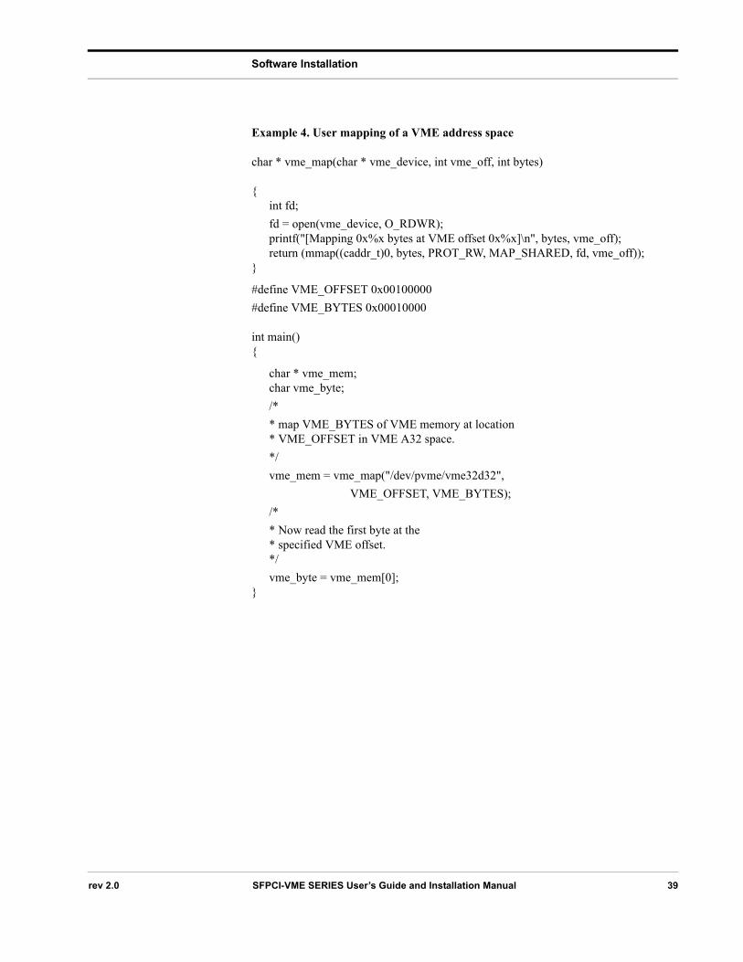
Example 4, “User mapping of a VME address space,” on page 35 illustrate show this might be done.
rev 2.0 SFPCI -VME SERIES User’s Guide and Installation Manual 38
Software Installation
Example 4. User mapping of a VME address space
char * vme_map(char * vme_device, int vme_off, int bytes)
{int fd;fd = open(vme_device, O_RDWR);printf("[Mapping 0x%x bytes at VME offset 0x%x]\n", bytes, vme_off);return (mmap((caddr_t)0, bytes, PROT_RW, MAP_SHARED, fd, vme_off));
}
#define VME_OFFSET 0x00100000#define VME_BYTES 0x00010000
int main(){
char * vme_mem;char vme_byte;/** map VME_BYTES of VME memory at location* VME_OFFSET in VME A32 space.*/vme_mem = vme_map("/dev/pvme/vme32d32",
VME_OFFSET, VME_BYTES); /** Now read the first byte at the* specified VME offset.*/vme_byte = vme_mem[0];
}
rev 2.0 SFPCI-VME SERIES User’s Guide and Installation Manual 39
Software Installation
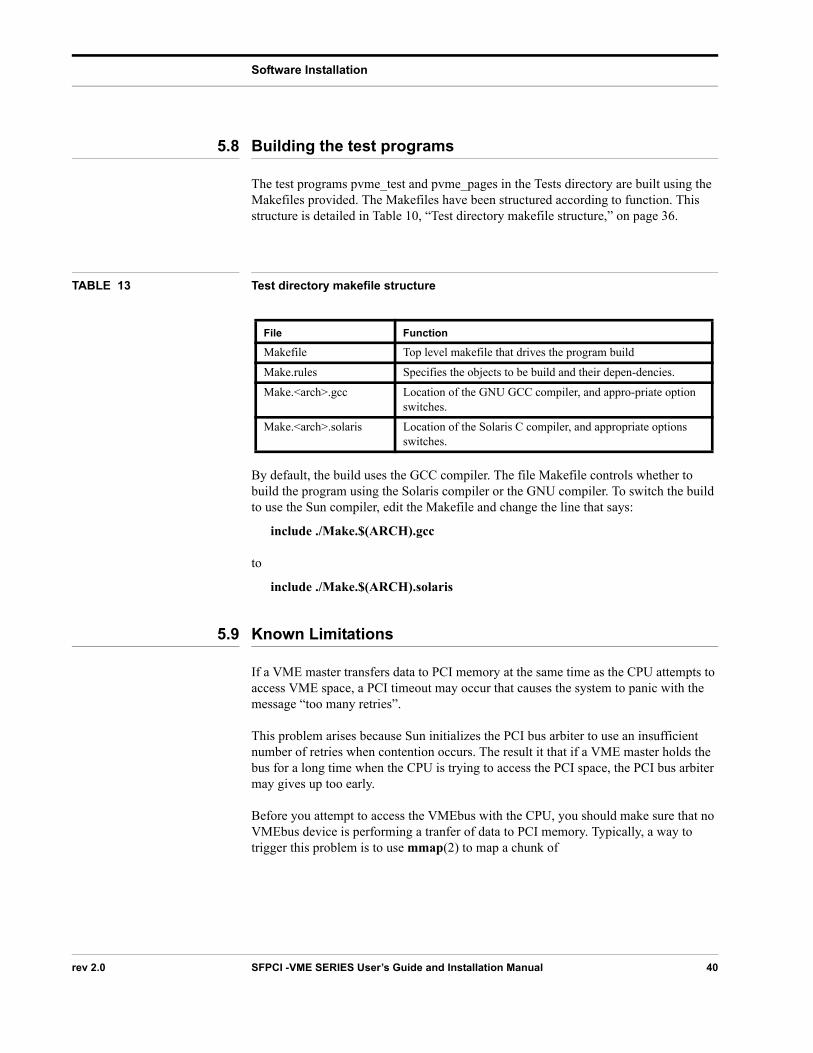
5.8 Building the test programs
The test programs pvme_test and pvme_pages in the Tests directory are built using the Makefiles provided. The Makefiles have been structured according to function. This structure is detailed in Table 10, “Test directory makefile structure,” on page 36.
By default, the build uses the GCC compiler. The file Makefile controls whether to build the program using the Solaris compiler or the GNU compiler. To switch the build to use the Sun compiler, edit the Makefile and change the line that says:
include ./Make.$(ARCH).gcc
to
include ./Make.$(ARCH).solaris
5.9 Known Limitations
If a VME master transfers data to PCI memory at the same time as the CPU attempts to access VME space, a PCI timeout may occur that causes the system to panic with the message “too many retries”.
This problem arises because Sun initializes the PCI bus arbiter to use an insufficient number of retries when contention occurs. The result it that if a VME master holds the bus for a long time when the CPU is trying to access the PCI space, the PCI bus arbiter may gives up too early.
Before you attempt to access the VMEbus with the CPU, you should make sure that no VMEbus device is performing a tranfer of data to PCI memory. Typically, a way to trigger this problem is to use mmap(2) to map a chunk of
TABLE 13 Test directory makefile structure
File Function
Makefile Top level makefile that drives the program build
Make.rules Specifies the objects to be build and their depen-dencies.
Make.<arch>.gcc Location of the GNU GCC compiler, and appro-priate option switches.
Make.<arch>.solaris Location of the Solaris C compiler, and appropriate options switches.
rev 2.0 SFPCI -VME SERIES User’s Guide and Installation Manual 40
Software Installation
VME memory into a program’s address space and then to access the mmaped VME memory it while a VME device is performing a DMA transfer. Such simultaneous attempts to access the VMEbus should be avoided by the user as much as possible.
rev 2.0 SFPCI-VME SERIES User’s Guide and Installation Manual 41
Byte Swapping Capability
CHAPTER 6 Byte Swapping Capability
6.1 General
The SF_VME board rev. F is a new member of the Solflower SFPCI-VME Adaptor series. It implements hardware byte swapping function to solve the problems inherent in joining Big and Little Endian buses. The SF_VME rev F is physically and electrically backward compatible with the older (rev D & E) revisions. The SFPCI-VME Bridge can be upgraded by simply replacing the VME card in the VME crate while PCI card and cable remain the same. Like its predecessors, SF_VME rev F needs to be installed in slot 1 in the VME crate in order to be a system controller, and fully function its byte swapping capability.
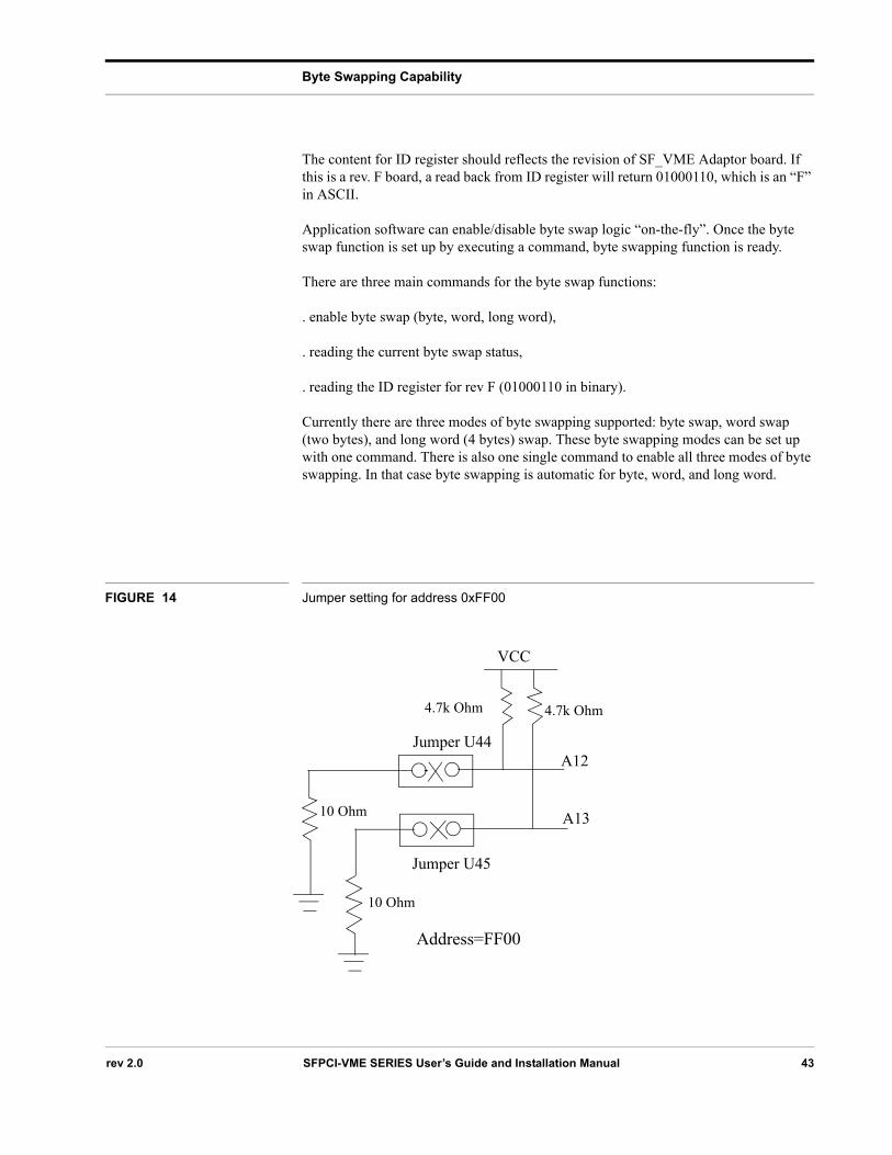
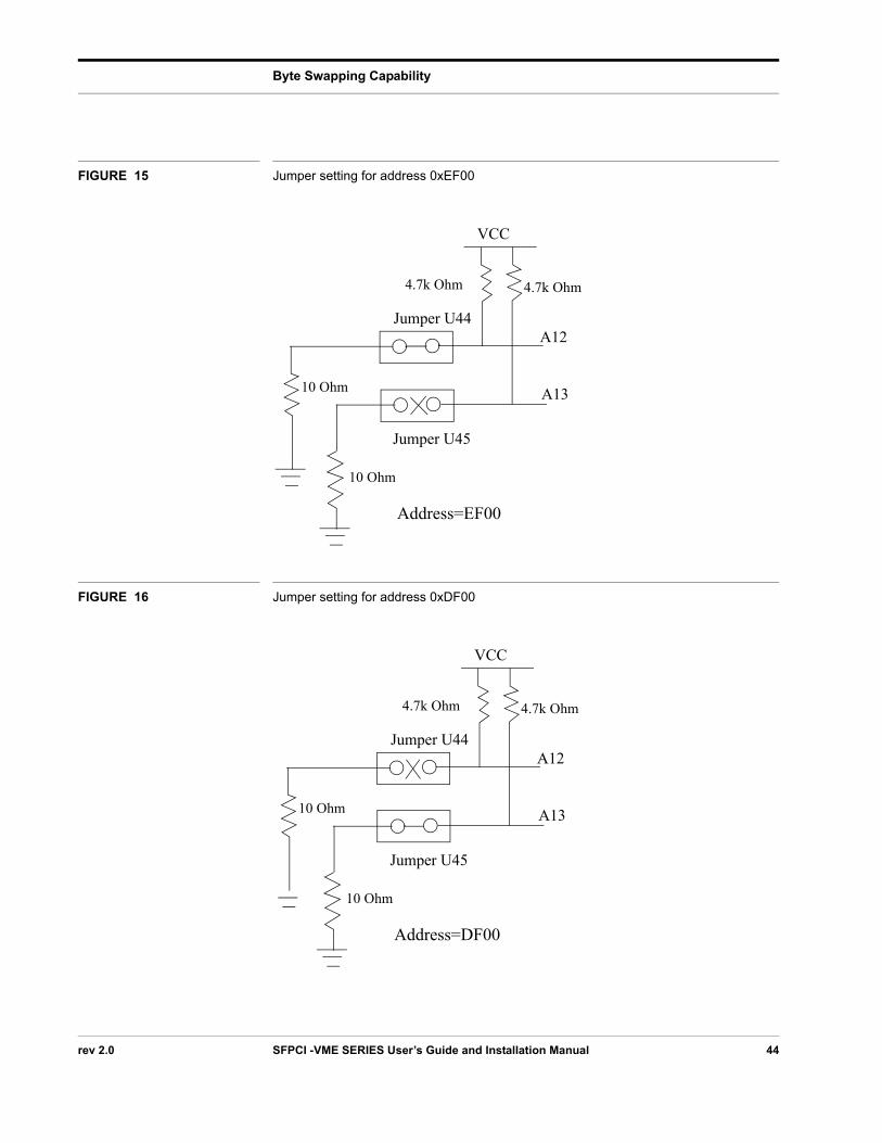
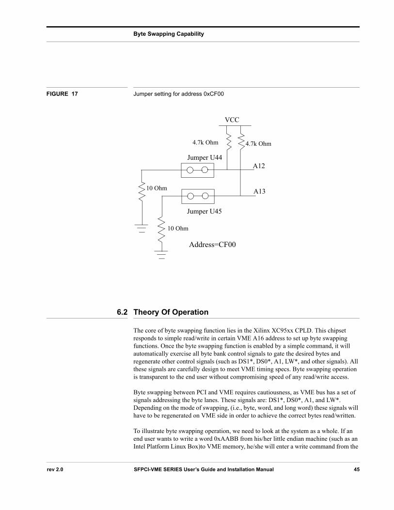
When byte swapping is disabled (by default), the SF_VME rev. F board acts like a SF_VME rev E or rev D board. This mode is used for Solaris system environment where data paths don't need to be swapped. The SF_VME rev. F board incorporates a Xilinx CPLD XC95xx. All the logics for byte swapping are implemented in XC95xx. Byte swapping function can be overwritten by on-board hardware jumper. All the byte swapping signals including DS1*, DS0*, A1, LW* and the controls of the byte lanes come from XC95xx. There will be three VME A16 addresses for byte swapping module’s register space: one for byte swapping command, one for status, and one for ID register. Command register sets up the byte swapping capability. Status register indicates the current status of the board. The content of the ID register indicates board revision. An A16 address for byte swapping can be set in the range CF00 to FF00, and is configurable with jumpers. (In fact, byte swapping address can be programmed in Solflower factory to any address space within 0x0000 to 0xFFFF.) Currently the default address is set to FF00. Command register is read/writable while status and ID register only allow reading. The address for command register is *F00 where (*) is configurable from C to F with jumpers. Similarly, address for status and ID registers are *F02, *F04 respectively. For more detail about jumper configurations, please refer to figure 14 to figure 17. The following table describes the contents and functions of command register. Byte swapping currently is not supported for D64, and Unaligned transfer.
TABLE 14 Byte Swapping Command Register
command[7:0] function
00001000 no swapping (power-up default)
00000xx1 enable byte swapping for byte
00000x10 enable byte swapping for word
000001xx enable byte swapping for long word
00000111 enable all swapping (byte, word, long word)
rev 2.0 SFPCI -VME SERIES User’s Guide and Installation Manual 42
Byte Swapping Capability
The content for ID register should reflects the revision of SF_VME Adaptor board. If this is a rev. F board, a read back from ID register will return 01000110, which is an “F” in ASCII.
Application software can enable/disable byte swap logic “on-the-fly”. Once the byte swap function is set up by executing a command, byte swapping function is ready.
There are three main commands for the byte swap functions:
. enable byte swap (byte, word, long word),
. reading the current byte swap status,
. reading the ID register for rev F (01000110 in binary).
Currently there are three modes of byte swapping supported: byte swap, word swap (two bytes), and long word (4 bytes) swap. These byte swapping modes can be set up with one command. There is also one single command to enable all three modes of byte swapping. In that case byte swapping is automatic for byte, word, and long word.
FIGURE 14 Jumper setting for address 0xFF00
Jumper U44
Jumper U45
A12
A13
VCC
Address=FF00
4.7k Ohm4.7k Ohm
10 Ohm
10 Ohm
rev 2.0 SFPCI-VME SERIES User’s Guide and Installation Manual 43
Byte Swapping Capability
FIGURE 15 Jumper setting for address 0xEF00
FIGURE 16 Jumper setting for address 0xDF00
Jumper U44
Jumper U45
A12
A13
VCC
Address=EF00
4.7k Ohm4.7k Ohm
10 Ohm
10 Ohm
Jumper U44
Jumper U45
A12
A13
VCC
Address=DF00
4.7k Ohm4.7k Ohm
10 Ohm
10 Ohm
rev 2.0 SFPCI -VME SERIES User’s Guide and Installation Manual 44
Byte Swapping Capability
FIGURE 17 Jumper setting for address 0xCF00
6.2 Theory Of Operation
The core of byte swapping function lies in the Xilinx XC95xx CPLD. This chipset responds to simple read/write in certain VME A16 address to set up byte swapping functions. Once the byte swapping function is enabled by a simple command, it will automatically exercise all byte bank control signals to gate the desired bytes and regenerate other control signals (such as DS1*, DS0*, A1, LW*, and other signals). All these signals are carefully design to meet VME timing specs. Byte swapping operation is transparent to the end user without compromising speed of any read/write access.
Byte swapping between PCI and VME requires cautiousness, as VME bus has a set of signals addressing the byte lanes. These signals are: DS1*, DS0*, A1, and LW*. Depending on the mode of swapping, (i.e., byte, word, and long word) these signals will have to be regenerated on VME side in order to achieve the correct bytes read/written.
To illustrate byte swapping operation, we need to look at the system as a whole. If an end user wants to write a word 0xAABB from his/her little endian machine (such as an Intel Platform Linux Box)to VME memory, he/she will enter a write command from the
Jumper U44
Jumper U45
A12
A13
VCC
Address=CF00
4.7k Ohm4.7k Ohm
10 Ohm
10 Ohm
rev 2.0 SFPCI-VME SERIES User’s Guide and Installation Manual 45
Byte Swapping Capability
keyboard. Once the end user hits enter key to execute the command, the CPU in the local machine will process this word and pass it downstream, maybe through a couple of PCI Bridges, and reaches the Universe PCI-VME Bridge. The Universe PCI-VME Bridge then processes this word and passes it to VME bus. Because the different endian between PCI (of an Intel Platform) and VME, this byte will appear on the VME side as 0xBBAA. This can be understood by looking at DS1*, DS0*, A1, and LW* signals on the VME bus. In this case the values for these signals will be 0, 0, 0,1 respectively. Since our goal is to write 0xAABB on VME bus, these signals will have to be manipulated and changed to different values in order to write to the right bytes on VME bus. This is the Xilinx XC95xx job to regenerate these four signals. Now they become 0, 0, 1, 1(DS1*, DS0*, A1, and LW*). These signals tell the VME memory to write the swapped bytes. Along with the four signals, bytes are gated through appropriate byte lanes by the control signals from XC95xx, and passed on to the VME bus. 0xAABB is then written to the VME memory.
6.3 Byte Swapping Detail
Currently rev F support three modes of byte swapping, namely, byte swapping for bytes, byte swapping for words, and byte swapping for long words. The following table describes swapping detail. Each swapping mode will be discussed in this section.
TABLE 15 Byte Swapping table
Byteswap behaviors:
In the table above "VME Address" is the address as seen by the VME Bus analyzer. "Host Data" is the result of the data being read from the VME into a register in the CPU. "Read Address (Host)" is the address read from the boards mapped into the host system's memory. "Width" is the number of bits read into the register.
No Byteswap (Little Endian) Register Byteswap (Little Endian)Read Address (Host)
Width VME Address Host Data VME Address Host Data
0xXXXXXXX0 32 0xXXXXXXX0 0xDDCCBBAA 0xXXXXXXX0 0xAABBCCDD0xXXXXXXX0 0xXXXXXXX0 0xBBAA 0xXXXXXXX0 0xAABB0xXXXXXXX2
16 0xXXXXXXX2 0xDDCC 0xXXXXXXX2 0xCCDD
0xXXXXXXX0 0xXXXXXXX0 0xAA 0xXXXXXXX0 0xAA0xXXXXXXX1 0xXXXXXXX1 0xBB 0xXXXXXXX1 0xBB0xXXXXXXX2 0xXXXXXXX2 0xCC 0xXXXXXXX2 0xCC0xXXXXXXX3
8
0xXXXXXXX3 0xDD 0xXXXXXXX3 0xDD
rev 2.0 SFPCI -VME SERIES User’s Guide and Installation Manual 46
Byte Swapping Capability
6.3.1 Byte Swapping for bytes:
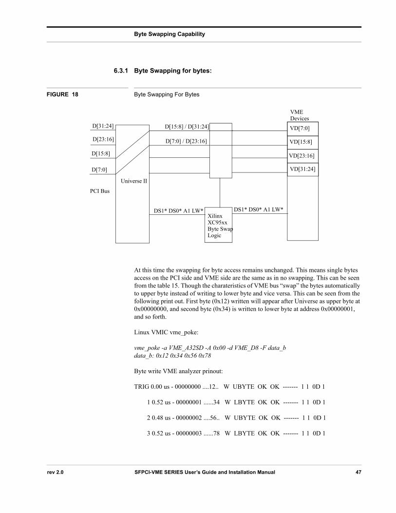
FIGURE 18 Byte Swapping For Bytes
At this time the swapping for byte access remains unchanged. This means single bytes access on the PCI side and VME side are the same as in no swapping. This can be seen from the table 15. Though the charateristics of VME bus “swap” the bytes automatically to upper byte instead of writing to lower byte and vice versa. This can be seen from the following print out. First byte (0x12) written will appear after Universe as upper byte at 0x00000000, and second byte (0x34) is written to lower byte at address 0x00000001, and so forth.
Linux VMIC vme_poke:
vme_poke -a VME_A32SD -A 0x00 -d VME_D8 -F data_b data_b: 0x12 0x34 0x56 0x78
Byte write VME analyzer prinout:
TRIG 0.00 us - 00000000 ....12.. W UBYTE OK OK ------- 1 1 0D 1
1 0.52 us - 00000001 ......34 W LBYTE OK OK ------- 1 1 0D 1
2 0.48 us - 00000002 ....56.. W UBYTE OK OK ------- 1 1 0D 1
3 0.52 us - 00000003 ......78 W LBYTE OK OK ------- 1 1 0D 1
Universe II
D[7:0]
D[15:8]
D[23:16]
D[31:24]
D[7:0] / D[23:16]
D[15:8] / D[31:24]
XilinxXC95xxByte SwapLogic
DS1* DS0* A1 LW*
VD[31:24]
VD[23:16]
VD[15:8]
VD[7:0]
VMEDevices
DS1* DS0* A1 LW*
PCI Bus
rev 2.0 SFPCI-VME SERIES User’s Guide and Installation Manual 47
Byte Swapping Capability
6.3.2 Byte swapping for words
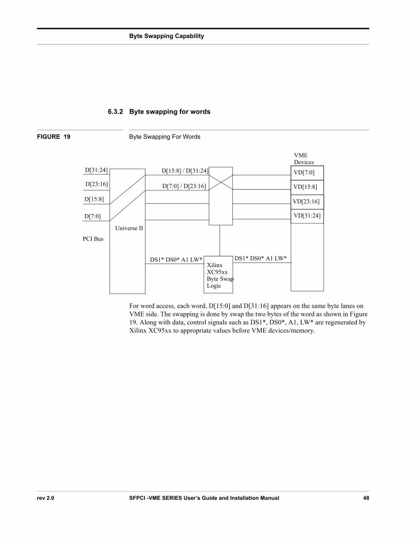
FIGURE 19 Byte Swapping For Words
For word access, each word, D[15:0] and D[31:16] appears on the same byte lanes on VME side. The swapping is done by swap the two bytes of the word as shown in Figure 19. Along with data, control signals such as DS1*, DS0*, A1, LW* are regenerated by Xilinx XC95xx to appropriate values before VME devices/memory.
Universe II
D[7:0]
D[15:8]
D[23:16]
D[31:24]
D[7:0] / D[23:16]
D[15:8] / D[31:24]
XilinxXC95xxByte SwapLogic
DS1* DS0* A1 LW*
VD[31:24]
VD[23:16]
VD[15:8]
VD[7:0]
VMEDevices
DS1* DS0* A1 LW*
PCI Bus
rev 2.0 SFPCI -VME SERIES User’s Guide and Installation Manual 48
Byte Swapping Capability
6.3.3 Byte swapping for long words
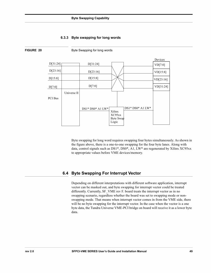
FIGURE 20 Byte Swapping for long words
Byte swapping for long word requires swapping four bytes simultaneously. As shown in the figure above, there is a one-to-one swapping for the four byte lanes. Along with data, control signals such as DS1*, DS0*, A1, LW* are regenerated by Xilinx XC95xx to appropriate values before VME devices/memory.
6.4 Byte Swapping For Interrupt Vector
Depending on different interpretations with different software application, interrupt vector can be masked out, and byte swapping for interrupt vector could be treated differently. Currently, SF_VME rev F. board treats the interrupt vector as in no swapping scenario, regardless whether the board was set to swapping mode or non-swapping mode. That means when interrupt vector comes in from the VME side, there will be no byte swapping for the interrupt vector. In the case when the vector is a one byte data, the Tundra Universe VME-PCI bridge on board will receive it as a lower byte data.
Universe II
D[7:0]
D[15:8]
D[23:16]
D[31:24]
D[23:16]
D[31:24]
XilinxXC95xxByte SwapLogic
DS1* DS0* A1 LW*
VD[31:24]
VD[23:16]
VD[15:8]
VD[7:0]
Devices
DS1* DS0* A1 LW*
PCI Bus
D[15:8]
D[7:0]
rev 2.0 SFPCI-VME SERIES User’s Guide and Installation Manual 49
Byte Swapping Capability
6.5 Byte Swapping Set Up Utility with Linux 2.4 Kernel
Solflower provides an utility program called “swp_ctl” to enable/disable byte swapping function. With SF_VME rev F installed and flat cable connected, power on the VME crate and your host that runs Linux 2.4 Kernel. The "swp_ctl" program is used to enable/disable hardware byte-swapping. When it's first started, it needs to know the address of the cmd register. There are jumpers on the board which allow us to set this address. The available range is from 0x0000CF00 to 0x0000FF00. After setting these jumpers, we can tell “swp_ctl” where the address is set. After byte swapping function is set up, user can run his/her own software to talk to VME devices. The following is an example of execution. Commands are in bold.
[root@localhost ]# ./swp_ctl
Type "?" for help.
Command
swp_ctl>?
-------
disable [bs|ws|ls|all] -- Disable swapping
enable [bs|ws|ls|all] -- Enable swapping
exit -- Exit swp_ctl
help -- Print command list with syntax
print [cmd|sta|bid] -- Display the specified register's state
? -- Print command list with syntax
quit -- Exit swp_ctl
set <address> -- Specified the address of the cmd register
swp_ctl> set ff00
cmd register address: 0x0000FF00
Now we can examine the cmd, status, and id registers.
swp_ctl> pr cmd sta bid
cmd register: 0x08FF
rev 2.0 SFPCI -VME SERIES User’s Guide and Installation Manual 50
Byte Swapping Capability
sta register: 0x05FF
bid register: 0x46FF
--0x46 is “F” in ASCII, stands for revision F.
These are the default values of these registers.
Here is the possible settings of the cmd register:
Values Meaning
-------------
0x01FF Enable byte-swap
0x02FF Enable word-swap
0x04FF Enable lword-swap
0x08FF Disable all swapping
0x07FF Enable all swapping
swp_ctl> disable [bs|ws|ls|all]
-- Disable swapping
swp_ctl> enable [bs|ws|ls|all]
-- Enable swapping
rev 2.0 SFPCI-VME SERIES User’s Guide and Installation Manual 51
System Specifications:
CHAPTER 7 System Specifications:
7.1 VME interface information
The VME interface board must always installed in VME chassis slot 1. As system controller, the VME interface board provides the following functions:
7.1.1 Bus arbitration
PCI-VME interface provides fix priority arbitration. BG3 is the highest request and selected as default.User can change the Bus Request level to BR0, BG1, BG2 as required
7.1.2 IACK
Only ROAK (Release On AcKnowledge) interrupting devices are supported Default VME interrupt level are set for IRQ1, IRQ2, IRQ3 and IRQ4.
7.1.3 SYSCLK
The PCI-VME provides 16MHZ SYSCLK signal to the VME bus.
7.1.4 Bus Timer
VME bus timeout is set to 1000us and bus arbitration timeout is set to 256us,
7.1.5 VME address spaces
Due to the PCI space available in the Sun Ultra machines, the entire A32 space cannot be mapped in to physical address space.
Only parts of the VME address space are available at any time. The limit on how large the A32 address space can be mapped are different in different system I/O configuration.
The A16 permits address from 0x0000 to 0xffffThe A24 permits address from 0x000000 to 1000000The A32 permits address range from 0x00000000 to max available on the PCI address space. VME transfers dma to PCI memory is set for 1MB window and supports both A24 and A32 spaces
rev 2.0 SFPCI -VME SERIES User’s Guide and Installation Manual 52
System Specifications:
7.1.6 AM codes
PCI-VME supports the following AM codes
2D Short supervisory access3D Standard supervisory data access3C Standard supervisory 64 bit block transfer0D Extended supervisory data access.0C Extended supervisory 64 bit block transfer
or
2D Short supervisory access3D Standard supervisory data access3F Standard supervisory block transfer0D Extended supervisory data access.0F Extended supervisory block transfer
7.1.7 Board Size 6U VME format 233mm x 160mm
7.1.8 Power Consumption less than 5W
7.1.9 Voltage 5V DC
7.2 6.2 PCI bus information
PCI-VME and uses the Universe chip, produced by Tundra Semiconductor as PCI controller. The universe is PCI 2.1 compliant. More specification about the Universe can be found at http://www.tundra.com/Tundra/unidex.html.
7.2.1 Size 6.875” x 4.2” short card
7.2.2 Bus clock Frequency 25 -33MHz
7.2.3 Data width 32/64bit
7.2.4 Voltage 5V DC
7.2.5 Power consumption less than 7.5W
rev 2.0 SFPCI-VME SERIES User’s Guide and Installation Manual 53
System Specifications:
7.3 VME chassis Specifications
7.3.1 6-slot VME enclosures dimension 14 ½” x 5 ½” x 12 ¼” (HxWxD)
450W auto-switching 110/220V AC 50/60Hz power supply
7.3.2 4-slot VME enclosure dimension 4” x 16” x 16” (HxWxD)
250W selectable 110/220V AC 50/60Hz power supply
7.4 Cable specifications
Cable are in 18”(1.5ft), 36” (3ft), 10ft, 15ft, 20ft, 24ft length, 100 pin flat ribbon shielded cable.
rev 2.0 SFPCI -VME SERIES User’s Guide and Installation Manual 54
Warranty and Repair
CHAPTER 8 Warranty and Repair
Solflower products are warranted against defective materials and workmanship within the warranty period of one year from date of invoice. Within the warranty period, Solflower will, free of charge, repair or replace any defective unit covered by this warranty, shipping prepaid. A Return of Materials Authorization number (RMA #) should be obtained from Solflower prior to the return of any defective product.
Solflower’s warranty is limited to the repair or replacement policy described above and neither Solflower or its agent shall be responsible for consequential or special damages related to the use of their products.
Any questions or requests for repair or technical support should be directed to:
Solflower Computer, Inc. 3511 Thomas Road, Ste-2 Santa Clara, CA 95054
Phone: (408) 982-8680 Fax: (408) 982-8685
rev 2.0 SFPCI-VME SERIES User’s Guide and Installation Manual 55
Warranty and Repair
rev 2.0 SFPCI -VME SERIES User’s Guide and Installation Manual 56