Embed Size (px)
Citation preview
VMEVME -- DPIO32DPIO32
32 digital Inputs or Outputs
HardwareHardware ManualManual
VME-DPIO32 Hardware Manual Rev. 2.1
N O T E
The information in this document has been carefully checked and isbelieved to be entirely reliable. esd makes no warranty of anykind with regard to the material in this document, and assumes noresponsibility for any errors that may appear in this document.esd reserves the right to make changes without notice to this, orany of its products, to improve reliability, performance ordesign.
esd assumes no responsibility for the use of any circuitry otherthan circuitry which is part of a product of esd gmbh.
esd does not convey to the purchaser of the product describedherein any license under the patent rights of esd gmbh nor therights of others.
esd electronic system design gmbhVahrenwalder Str. 205
D-30165 HannoverGermany
Phone: +49-511-372980FAX: +49-511-633650
This document shall not be duplicated, nor its contents usedfor any purpose, unless express permission has been granted.Copyright by esd
VME-DPIO32 Hardware Manual Rev. 2.1
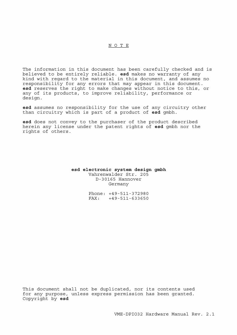
Manual File: i:\texte\doku\manuals\vme\dpio32\dpio21h.eng 29.07.97
Described DPI32-5PCB version S/N AB043 and later
Changes in the chapters
The changes in the user’s manual listed below affect changes inthe firmware, as well as changes in the description of the factsonly.
Chapter Change
2. Chapter ’Software’ now a separate document.
Further technical changes are subject to change without notice.
VME-DPIO32 Hardware Manual Rev. 2.1

VME-DPIO32 Hardware Manual Rev. 2.1
User’s Manual DPIO32
Content Page
1. Hardware . . . . . . . . . . . . . . . . . . . . . . . . . . 3
1.1 Overview . . . . . . . . . . . . . . . . . . . . . . . 31.1.1 Board Description . . . . . . . . . . . . . . . 31.1.2 Summary of Technical Data . . . . . . . . . . . 51.1.3 Software Support . . . . . . . . . . . . . . . 8
1.2 Order Information . . . . . . . . . . . . . . . . . . 9
1.3 Address Covering of VME-DPIO32 . . . . . . . . . . . . 11
1.4 Jumpers Configuration . . . . . . . . . . . . . . . . 131.4.1 Default Setting . . . . . . . . . . . . . . . . 141.4.2 The Address-Modifier AM Jumper J3 . . . . . . . 151.4.3 Basic Address Decoding via the Jumpers J1 and
J2 . . . . . . . . . . . . . . . . . . . . . . . 19
1.5 Interrupt Processing . . . . . . . . . . . . . . . . . 21
1.6 The Digital Inputs and Outputs . . . . . . . . . . . . 231.6.1 Controller Assignment to Inputs and Outputs . . 231.6.2 Pulse Processor HD63143 Structure . . . . . . . 251.6.3 Input and Output Circuit of DPIO32 . . . . . . 27
1.6.3.1 General . . . . . . . . . . . . . . . . 271.6.3.2 Front Panel LEDs and Test Sockets . . . 291.6.3.3 Input and Output Circuit Diagram . . . . 30
2. Appendix . . . . . . . . . . . . . . . . . . . . . . . . . . 31
2.1 Connector Pin Assigments . . . . . . . . . . . . . . . 312.1.1 VMEbus P1 . . . . . . . . . . . . . . . . . . . 312.1.2 I/O Connector P2 . . . . . . . . . . . . . . . 322.1.3 Terminal Block I/O Connector P2 Phönix FLKM64
or FLKMS64 . . . . . . . . . . . . . . . . . . . 332.1.4 Description of the Signals at the I/O Connector
P2 (or Terminal Block) . . . . . . . . . . . . . 342.1.5 Wiring Diagrams . . . . . . . . . . . . . . . . 35
2.2 Front Panel . . . . . . . . . . . . . . . . . . . . . 39
2.3 Circuit Diagrams . . . . . . . . . . . . . . . . . . . 41
2.4 Data Sheets . . . . . . . . . . . . . . . . . . . . . 43
VME-DPIO32 Hardware Manual Rev. 2.1 1

VME-DPIO32 Hardware Manual Rev. 2.12
Overview
1. Hardware
1.1 Overview
1.1.1 Board Description
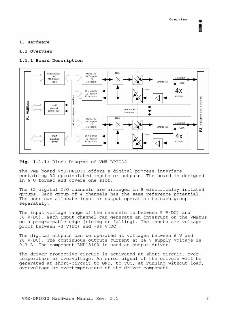
Fig. 1.1.1: Block Diagram of VME-DPIO32
VME addressand
AM decoderlogic
VMEinterrupt
control logic
VME data bus
driver
P1
VM
Ebu
s
addr
ess,
dat
a an
d co
ntro
l bus
HD6314316 Outputs
or16 Inputs
CIO Z853616 Inputs+Error Input
CIO Z853616 Inputs+Error Input
P2
8 gr
oup
s of
eac
h 4
chan
nels
MUX
LMD18400
Error
4xInput
4xOutput
MUX
LMD18400
Error
4xInput
4xOutput
4x
electricalisolation
4x
HD6314316 Outputs
or16 Inputs VCC
VCC
The VME board VME-DPIO32 offers a digital process interfacecontaining 32 optoisolated inputs or outputs. The board is designedin 6 U format and covers one slot.
The 32 digital I/O channels are arranged in 8 electrically isolatedgroups. Each group of 4 channels has the same reference potential.The user can allocate input or output operation to each groupseparately.
The input voltage range of the channels is between 5 V(DC) and30 V(DC). Each input channel can generate an interrupt on the VMEbuson a programmable edge (rising or falling). The inputs are voltage-proof between -3 V(DC) and +36 V(DC).
The digital outputs can be operated at voltages between 6 V and28 V(DC). The continuous outputs current at 24 V supply voltage is0.3 A. The component LMD18400 is used as output driver.
The driver protective circuit is activated at short-circuit, over-temperature or overvoltage. An error signal of the drivers will begenerated at short-circuit to GND, to VCC, at running without load,overvoltage or overtemperature of the driver component.
VME-DPIO32 Hardware Manual Rev. 2.1 3
Overview
In addition to the bit-programmable operating mode of the outputs,it is possible to use the single output channels via the pulseprocessor components HD63143 for pulse-width modulation (PWM). Atotal of 2 x 24 programmable 16 bit registers are available forswitching period and resolution. The minimum switching periodamounts to 10 µs. The outputs can mutually be synchronised.
A total of 20 digital counter inputs of the controllers isavailable. At this, four of which are connected in parallel to CIO8536 and to HD63143. The maximum counter frequency for these fourCIO counters is 3 MHz. Depending on the operating mode, the HD63143counters can process frequencies from 100 kHz to 1 MHz. For thecounter inputs various operating modes are possible (event counter,pulse-width measurement, frequency measurement, free running withinterrupt, incremental encoder inputs etc.).
The actual I/O status of the inputs and outputs is displayed on thefront panel of VME-DPIO32 by a two-colored LED for each channel, theerror status is displayed group-wise. Additionally there are testsockets for each channel located on the front panel for simulationof the input signals or for disable of the error messages.
VME-DPIO32 Hardware Manual Rev. 2.14
Overview
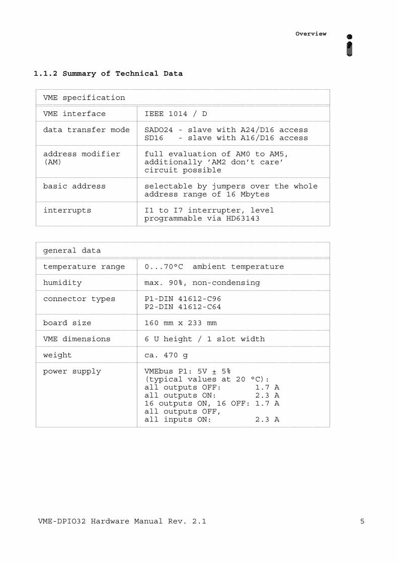
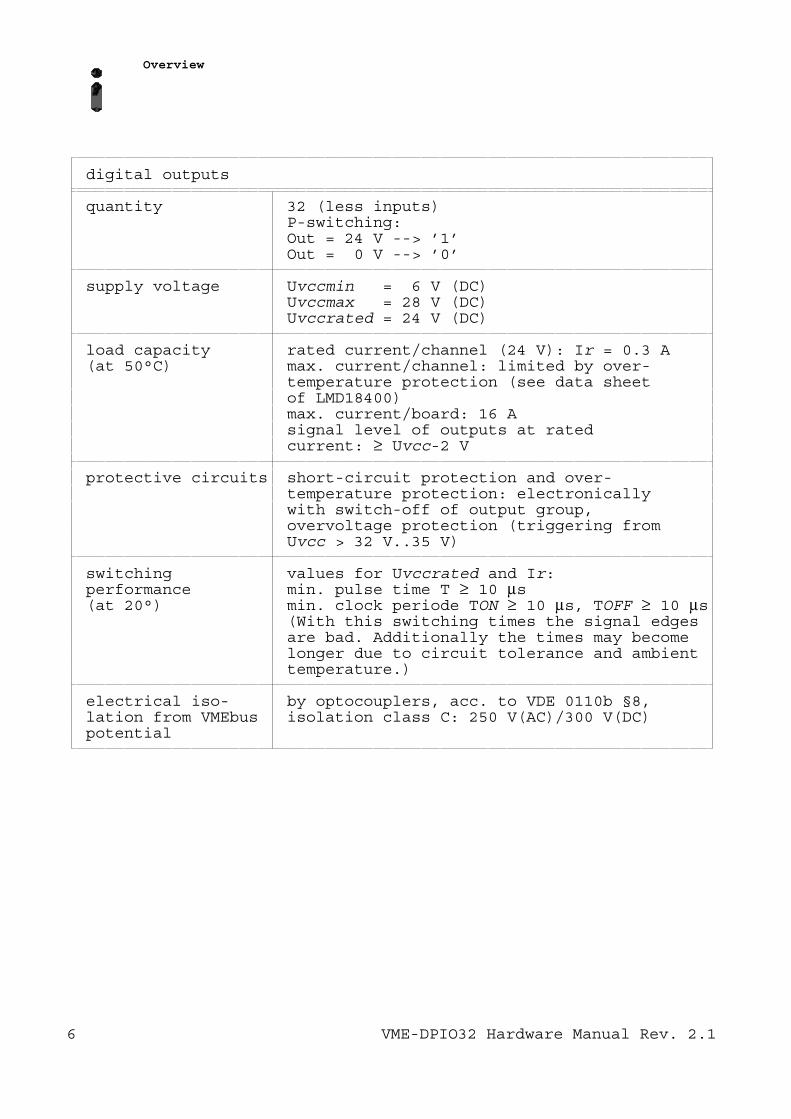
1.1.2 Summary of Technical Data
VME specification
VME interface IEEE 1014 / D
data transfer mode SADO24 - slave with A24/D16 accessSD16 - slave with A16/D16 access
address modifier full evaluation of AM0 to AM5,(AM) additionally ’AM2 don’t care’
circuit possible
basic address selectable by jumpers over the wholeaddress range of 16 Mbytes
interrupts I1 to I7 interrupter, levelprogrammable via HD63143
general data
temperature range 0...70°C ambient temperature
humidity max. 90%, non-condensing
connector types P1-DIN 41612-C96P2-DIN 41612-C64
board size 160 mm x 233 mm
VME dimensions 6 U height / 1 slot width
weight ca. 470 g
power supply VMEbus P1: 5V ± 5%(typical values at 20 °C):all outputs OFF: 1.7 Aall outputs ON: 2.3 A16 outputs ON, 16 OFF: 1.7 Aall outputs OFF,all inputs ON: 2.3 A
VME-DPIO32 Hardware Manual Rev. 2.1 5
Overview
digital outputs
quantity 32 (less inputs)P-switching:Out = 24 V --> ’1’Out = 0 V --> ’0’
supply voltage Uvccmin = 6 V (DC)Uvccmax = 28 V (DC)Uvccrated = 24 V (DC)
load capacity rated current/channel (24 V): Ir = 0.3 A(at 50°C) max. current/channel: limited by over-
temperature protection (see data sheetof LMD18400)max. current/board: 16 Asignal level of outputs at ratedcurrent: ≥ Uvcc-2 V
protective circuits short-circuit protection and over-temperature protection: electronicallywith switch-off of output group,overvoltage protection (triggering fromUvcc > 32 V..35 V)
switching values for Uvccrated and Ir:performance min. pulse time T ≥ 10 µs(at 20°) min. clock periode TON ≥ 10 µs, TOFF ≥ 10 µs
(With this switching times the signal edgesare bad. Additionally the times may becomelonger due to circuit tolerance and ambienttemperature.)
electrical iso- by optocouplers, acc. to VDE 0110b §8,lation from VMEbus isolation class C: 250 V(AC)/300 V(DC)potential
VME-DPIO32 Hardware Manual Rev. 2.16
Overview
digital inputs (part 1)
quantity 32 (less outputs)
evaluation all inputs have interrupt capabilitymax. 16 inputs at P2 configurable ascounter inputs, all 16 inputsconnected to HD63143 and additionally4 inputs in parallel to CIO Z8536(higher resolution)
input voltage permissible input voltage range:-3 V ≤ Uin ≤ 30 VAttention: If output driver LMD18400is supplied by Uvccout,Uin may notexceed Uin ≤ Uvccout - 2V !(because of parallel connection tooutputs)
threshold input = ’0’:Uout ≤ 2.0V
threshold input = ’1’:Uin ≥ 3.0V
input current Since the inputs and outputs areconnected in parallel on the board,the input current depends on the fact,whether the supply voltage is con-nected to the output driver LMD18400:
input current/channel at Uvcc = 24 V(typical values at 20 °C):input = ’1’: (5 V) Iin = 7.7 mA
(12 V) Iin = 9.9 mA(22 V) Iin = 10.0 mA
input current/channel at Uvcc notsupplied (typical values at 20 °C):input = ’1’: (5 V) Iin = 8.0 mA
(12 V) Iin = 14.0 mA(24 V) Iin = 30.0 mA(30 V) Iin = 40.0 mA
VME-DPIO32 Hardware Manual Rev. 2.1 7
Overview
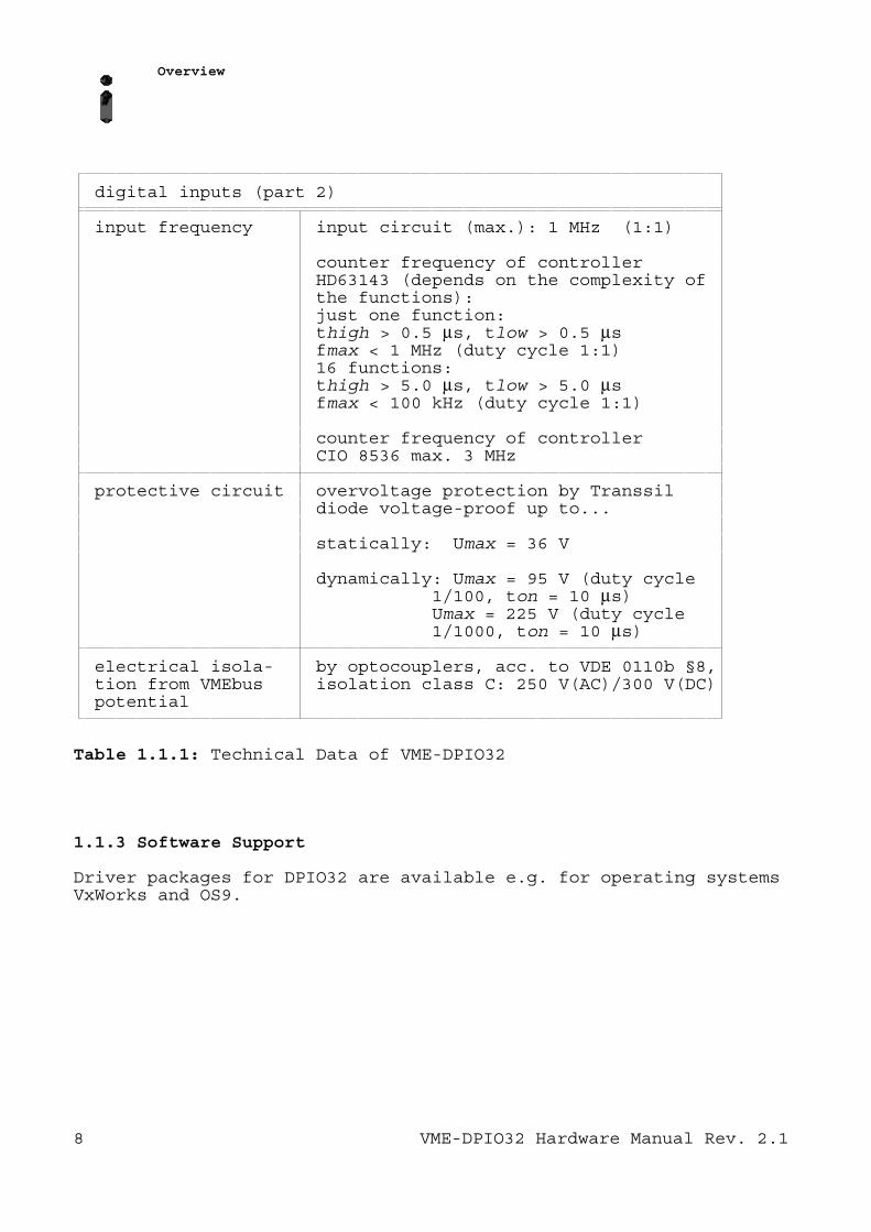
digital inputs (part 2)
input frequency input circuit (max.): 1 MHz (1:1)
counter frequency of controllerHD63143 (depends on the complexity ofthe functions):just one function:thigh > 0.5 µs, tlow > 0.5 µsfmax < 1 MHz (duty cycle 1:1)16 functions:thigh > 5.0 µs, tlow > 5.0 µsfmax < 100 kHz (duty cycle 1:1)
counter frequency of controllerCIO 8536 max. 3 MHz
protective circuit overvoltage protection by Transsildiode voltage-proof up to...
statically: Umax = 36 V
dynamically: Umax = 95 V (duty cycle1/100, ton = 10 µs)Umax = 225 V (duty cycle1/1000, ton = 10 µs)
electrical isola- by optocouplers, acc. to VDE 0110b §8,tion from VMEbus isolation class C: 250 V(AC)/300 V(DC)potential
Table 1.1.1: Technical Data of VME-DPIO32
1.1.3 Software Support
Driver packages for DPIO32 are available e.g. for operating systemsVxWorks and OS9.
VME-DPIO32 Hardware Manual Rev. 2.18
Order Information
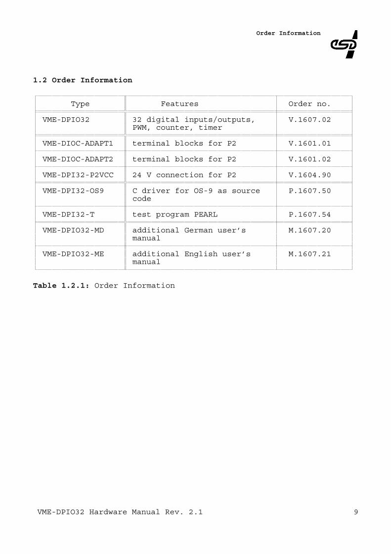
1.2 Order Information
Type Features Order no.
VME-DPIO32 32 digital inputs/outputs, V.1607.02PWM, counter, timer
VME-DIOC-ADAPT1 terminal blocks for P2 V.1601.01
VME-DIOC-ADAPT2 terminal blocks for P2 V.1601.02
VME-DPI32-P2VCC 24 V connection for P2 V.1604.90
VME-DPI32-OS9 C driver for OS-9 as source P.1607.50code
VME-DPI32-T test program PEARL P.1607.54
VME-DPIO32-MD additional German user’s M.1607.20manual
VME-DPIO32-ME additional English user’s M.1607.21manual
Table 1.2.1: Order Information
VME-DPIO32 Hardware Manual Rev. 2.1 9

VME-DPIO32 Hardware Manual Rev. 2.110
Address Covering
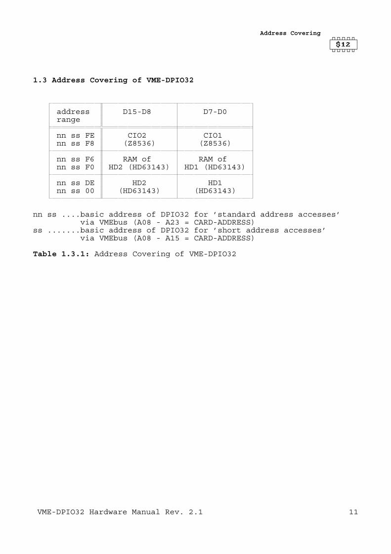
1.3 Address Covering of VME-DPIO32
address D15-D8 D7-D0range
nn ss FE CIO2 CIO1nn ss F8 (Z8536) (Z8536)
nn ss F6 RAM of RAM ofnn ss F0 HD2 (HD63143) HD1 (HD63143)
nn ss DE HD2 HD1nn ss 00 (HD63143) (HD63143)
nn ss ....basic address of DPIO32 for ’standard address accesses’via VMEbus (A08 - A23 = CARD-ADDRESS)
ss .......basic address of DPIO32 for ’short address accesses’via VMEbus (A08 - A15 = CARD-ADDRESS)
Table 1.3.1: Address Covering of VME-DPIO32
VME-DPIO32 Hardware Manual Rev. 2.1 11

VME-DPIO32 Hardware Manual Rev. 2.112
Jumpers Configuration
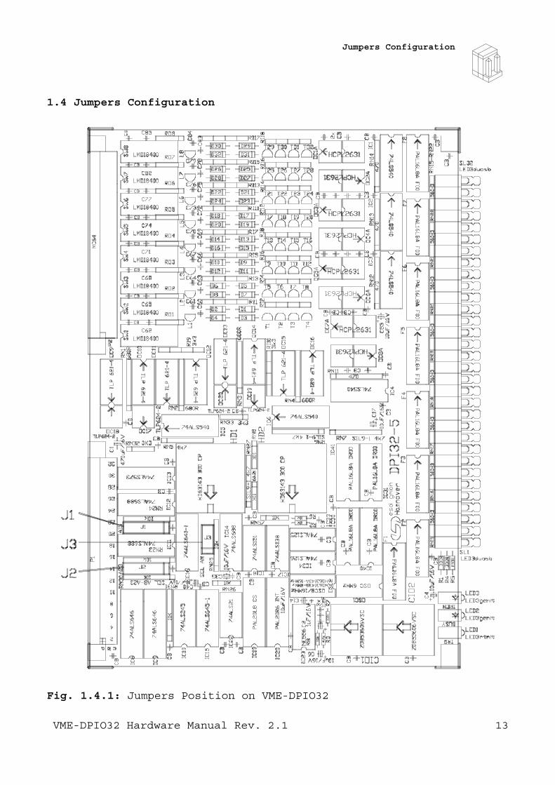
1.4 Jumpers Configuration
Fig. 1.4.1: Jumpers Position on VME-DPIO32
VME-DPIO32 Hardware Manual Rev. 2.1 13
Jumpers Configuration
1.4.1 Default Setting
The particular factory-settings (of the jumpers see following table)are marked in the table.
The jumpers configuration can be obtained from the insertiondiagram.An inserted jumper corresponds to ’0’ (low) level of a signal.
In the following the jumpers are displayed in a position, as seen bythe user, if he has the board lying in front of himself with theVMEbus connectors to the rear end.
Default jumper setting of jumpers J1 to J4:
jumper function setting
J1 basic addressA08-A15
basic address of DPIO32 setto $xxE14000
J2 basic addressA16-A23
J3 address modifier AM2 don’t care, i.e. accessin the supervisory mode oruser mode VME access A24/D16
Table 1.4.1: Default Jumper Setting
VME-DPIO32 Hardware Manual Rev. 2.114
Jumpers Configuration
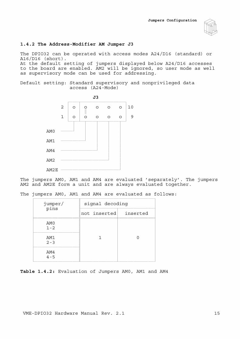
1.4.2 The Address-Modifier AM Jumper J3
The DPIO32 can be operated with access modes A24/D16 (standard) orA16/D16 (short).At the default setting of jumpers displayed below A24/D16 accessesto the board are enabled. AM2 will be ignored, so user mode as wellas supervisory mode can be used for addressing.
Default setting: Standard supervisory and nonprivileged dataaccess (A24-Mode)
J3
2 o o o o o 10
1 o o o o o 9
AM0
AM1
AM4
AM2
AM2E
The jumpers AM0, AM1 and AM4 are evaluated ’separately’. The jumpersAM2 and AM2E form a unit and are always evaluated together.
The jumpers AM0, AM1 and AM4 are evaluated as follows:
jumper/ signal decodingpins
not inserted inserted
AM01-2
AM1 1 02-3
AM44-5
Table 1.4.2: Evaluation of Jumpers AM0, AM1 and AM4
VME-DPIO32 Hardware Manual Rev. 2.1 15
Jumpers Configuration
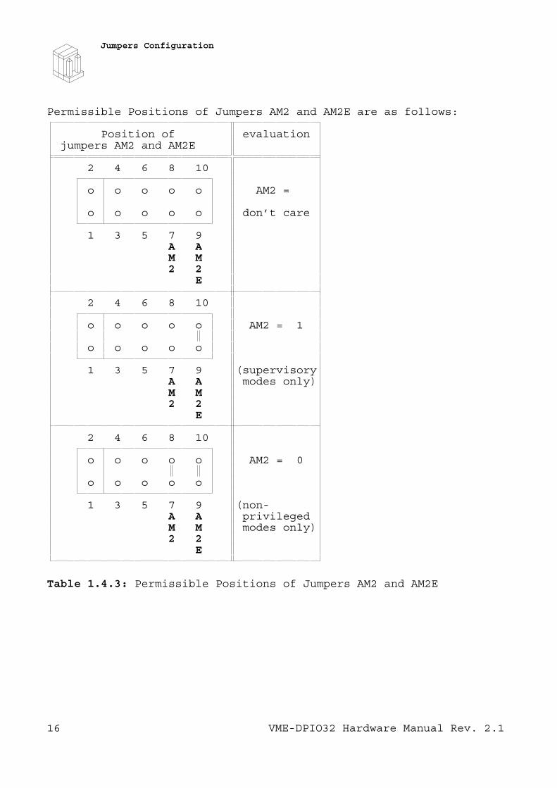
Permissible Positions of Jumpers AM2 and AM2E are as follows:
Position of evaluationjumpers AM2 and AM2E
2 4 6 8 10
o o o o o AM2 =
o o o o o don’t care
1 3 5 7 9A AM M2 2
E
2 4 6 8 10
o o o o o AM2 = 1
o o o o o
1 3 5 7 9 (supervisoryA A modes only)M M2 2
E
2 4 6 8 10
o o o o o AM2 = 0
o o o o o
1 3 5 7 9 (non-A A privilegedM M modes only)2 2
E
Table 1.4.3: Permissible Positions of Jumpers AM2 and AM2E
VME-DPIO32 Hardware Manual Rev. 2.116
Jumpers Configuration
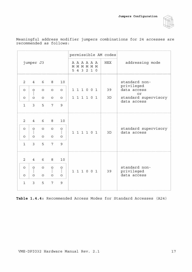
Meaningful address modifier jumpers combinations for 24 accesses arerecommended as follows:
permissible AM codes
jumper J3 A A A A A A HEX addressing modeM M M M M M5 4 3 2 1 0
2 4 6 8 10 standard non-privileged
o o o o o 1 1 1 0 0 1 39 data accessor
o o o o o 1 1 1 1 0 1 3D standard supervisorydata access
1 3 5 7 9
2 4 6 8 10
o o o o o standard supervisory1 1 1 1 0 1 3D data access
o o o o o
1 3 5 7 9
2 4 6 8 10
o o o o o standard non-1 1 1 0 0 1 39 privileged
o o o o o data access
1 3 5 7 9
Table 1.4.4: Recommended Access Modes for Standard Accesses (A24)
VME-DPIO32 Hardware Manual Rev. 2.1 17
Jumpers Configuration
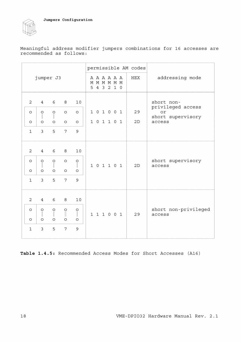
Meaningful address modifier jumpers combinations for 16 accesses arerecommended as follows:
permissible AM codes
jumper J3 A A A A A A HEX addressing modeM M M M M M5 4 3 2 1 0
2 4 6 8 10 short non-privileged access
o o o o o 1 0 1 0 0 1 29 orshort supervisory
o o o o o 1 0 1 1 0 1 2D access
1 3 5 7 9
2 4 6 8 10
o o o o o short supervisory1 0 1 1 0 1 2D access
o o o o o
1 3 5 7 9
2 4 6 8 10
o o o o o short non-privileged1 1 1 0 0 1 29 access
o o o o o
1 3 5 7 9
Table 1.4.5: Recommended Access Modes for Short Accesses (A16)
VME-DPIO32 Hardware Manual Rev. 2.118
Jumpers Configuration
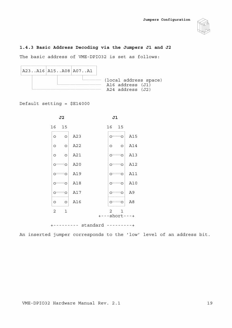
1.4.3 Basic Address Decoding via the Jumpers J1 and J2
The basic address of VME-DPIO32 is set as follows:
A23..A16 A15..A08 A07..A1
(local address space)A16 address (J1)A24 address (J2)
Default setting = $E14000
J2 J1
16 15 16 15
o o A23 o o A15
o o A22 o o A14
o o A21 o o A13
o o A20 o o A12
o o A19 o o A11
o o A18 o o A10
o o A17 o o A9
o o A16 o o A8
2 1 2 1+---short---+
+--------- standard ---------+
An inserted jumper corresponds to the ’low’ level of an address bit.
VME-DPIO32 Hardware Manual Rev. 2.1 19

VME-DPIO32 Hardware Manual Rev. 2.120
Interrupt Processing
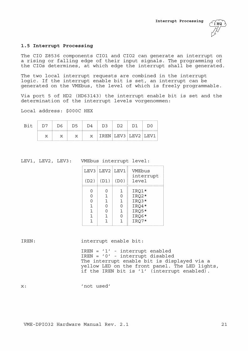
1.5 Interrupt Processing
The CIO Z8536 components CIO1 and CIO2 can generate an interrupt ona rising or falling edge of their input signals. The programming ofthe CIOs determines, at which edge the interrupt shall be generated.
The two local interrupt requests are combined in the interruptlogic. If the interrupt enable bit is set, an interrupt can begenerated on the VMEbus, the level of which is freely programmable.
Via port 5 of HD2 (HD63143) the interrupt enable bit is set and thedetermination of the interrupt levels vorgenommen:
Local address: $000C HEX
Bit D7 D6 D5 D4 D3 D2 D1 D0
x x x x IREN LEV3 LEV2 LEV1
LEV1, LEV2, LEV3: VMEbus interrupt level:
LEV3 LEV2 LEV1 VMEbusinterrupt
(D2) (D1) (D0) level
0 0 1 IRQ1*0 1 0 IRQ2*0 1 1 IRQ3*1 0 0 IRQ4*1 0 1 IRQ5*1 1 0 IRQ6*1 1 1 IRQ7*
IREN: interrupt enable bit:
IREN = ’1’ - interrupt enabledIREN = ’0’ - interrupt disabledThe interrupt enable bit is displayed via ayellow LED on the front panel. The LED lights,if the IREN bit is ’1’ (interrupt enabled).
x: ’not used’
VME-DPIO32 Hardware Manual Rev. 2.1 21

VME-DPIO32 Hardware Manual Rev. 2.122
Digital I/Os
1.6 The Digital Inputs and Outputs
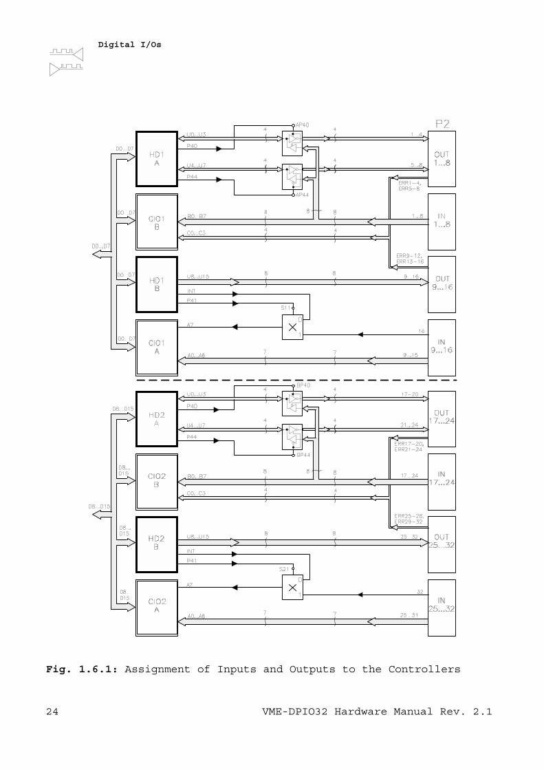
1.6.1 Controller Assignment to Inputs and Outputs
The DPIO32 is equipped with 4 controller components. The two CIOZ8536 controllers handle the digital inputs and together offer twotimers/counters with a maximum input frequency of 3 MHz each.
Two HD63143 supply the digital outputs. The operating modes ’digitaloutput’ or ’pulse width modulated output’ are possible.The HD63143 can also process input signals via multiplexers.Moreover they make available a total of 16 counters with a maximumcounter frequency of 100 kHz (duty cycle 1:1) each.If the HD63143 controllers shall generate VMEbus interrupts, thentheir interrupt outputs are fed to the CIO Z8536 port A7. Theinterrupt handling on the VMEbus is processed via the CIO.
Fig. 1.6.1 displays the assignment of inputs and outputs on the VME-DPIO32. The designations ’IN...’ and ’OUT...’ in column P2 displaythe input and output numbers, where inputs and outputs with the samenumber physically cover the same pin on the P2 connector.
The multiplexers for input or output operation of HD63143 portsU0...U7 and for the interrupt output of HD63143 are driven by portsP40...P44. The following tables indicate the multiplexer functions,which are identical for both HD63143 controllers:
HD63143 port HD63143 port HD63143 port HD63143 portP40 U0...U3 P44 U4...U7
0 input 0 input
1 output 1 output
Table 1.6.1: Switching of Ports U0...U7 Data Direction(corresponds to channels 1...8, or 17...24)
HD63143 port CIO Z8536 port A7P41
0 port A7 is used by HD63143 for VMEbus interruptgeneration
1 reserved
Table 1.6.2: CIO Z8536 Input Port A7 Covering
VME-DPIO32 Hardware Manual Rev. 2.1 23
Digital I/Os
Fig. 1.6.1: Assignment of Inputs and Outputs to the Controllers
VME-DPIO32 Hardware Manual Rev. 2.124
Digital I/Os
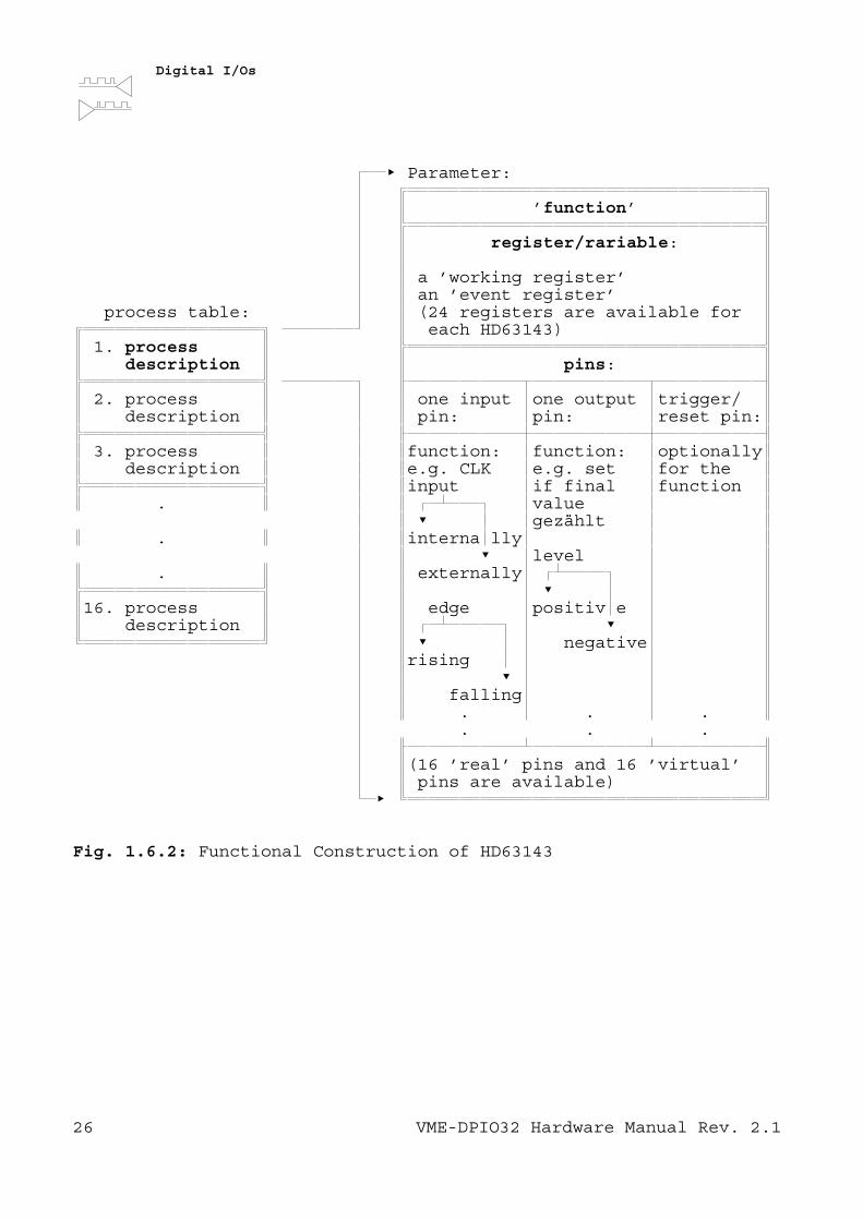
1.6.2 Pulse Processor HD63143 Structure
The HD63143 mainly consists of three functional units: The universalpulse processor, two serial interfaces and a RAM of 1024.
The serial interfaces are not used on the DPIO32. The HD63143 RAM isnot available to the user in PCB version DPI32-5.
The internal pulse processor disposes of an own 16 bit wide ALU(Arithmetic Logik Unit). The principal pulse processor function canbe illustrated by a scheme, which builds up on a process table:
The HD63143 continuously runs the instructions of a process table,where up to 16 process descriptions can be listed. Each of theseprocess descriptions contains informations (parameters) on a desiredfunction.
These parameters contain e.g. the registers to be used, the usedpins and functions assigned to the pins.
The following figure displays this construction again as a survey. Acomplete listing of all possible parameters can be obtained from thesoftware description.
VME-DPIO32 Hardware Manual Rev. 2.1 25
Digital I/Os
Parameter:
’function’
register/rariable:
a ’working register’an ’event register’
process table: (24 registers are available foreach HD63143)
1. processdescription pins:
2. process one input one output trigger/description pin: pin: reset pin:
3. process function: function: optionallydescription e.g. CLK e.g. set for the
input if final function. value
gezählt. interna lly
level. externally
16. process edge positiv edescription
negativerising
falling. . .. . .
(16 ’real’ pins and 16 ’virtual’pins are available)
Fig. 1.6.2: Functional Construction of HD63143
VME-DPIO32 Hardware Manual Rev. 2.126
Digital I/Os
1.6.3 Input and Output Circuit of DPIO32
1.6.3.1 General
The DPIO32 is designed for 32 input or output channels. Each of the32 channels can be operated either as input or output.
If a channel is operated as output, then the signal condition of theoutput can be read-back ’online’ via the input circuit, which isconnected in parallel.
The channels are configured in groups of four, because each 4outputs are supplied by one driver component. If a channel groupshall operate as input group, all outputs of this group must be setto ’0’.
If at input operation of an I/O group no power supply is connectedto the corresponding output driver, a part of the input current willflow into the output driver. In this case the input currentconsumption will increase. Thus it is recommended to connect a powersupply to the output drivers of an I/O group as well when operatingthis group as inputs only.The input voltage in this case may not exceed a maximum equal toUvccout - 2V because otherwise the output drivers might bedestroyed!
As output driver a LMD18400 is used. The driver component canconnect voltages of 6V to 28V (HIGH level) to GND.The output driver supply voltage must be supplied externally. Each 4of 32 channels are connected to one voltage supply. With this, 8different output groups, optoisolated from each other, are possible.
Each of the 8 output drivers disposes of an error output, which willbe triggered on occurence of an error at one or several channels.The error outputs are connected to the C ports of the two CIO Z8536.
VME-DPIO32 Hardware Manual Rev. 2.1 27
Digital I/Os
error signal of atthe outputs CIO/Port
1...4 CIO1/PC0
5...8 CIO1/PC1
9...12 CIO1/PC2
13...16 CIO1/PC3
17...20 CIO2/PC0
21...24 CIO2/PC1
25...28 CIO2/PC2
29...32 CIO2/PC3
Table 1.6.3: Connection of the Error Signals to the CIO Ports
An error output will be triggered at the following operatingtroubles:
- no load- short-circuit to VCC or GND- overvoltage- overtemperature of the driver component
Comment to error handling:If the error conditions ’overtemperature’ or ’supply voltage toohigh’ occor, the LMD18400 switches off all 4 outputs. If the errorcondition is no longer valid and the inputs of the driver are stillactive, the LMD18400 switches automatically the outputs on again.
The error condition ’unloaded output’ will not be detected: Theoutputs are connected to the inputs and therefore the outputs arecontinously loaded with the small load of the input circuits.
VME-DPIO32 Hardware Manual Rev. 2.128
Digital I/Os
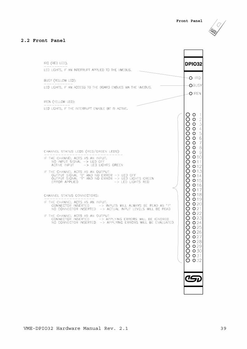
1.6.3.2 Front Panel LEDs and Test Sockets
The channel status is displayed by two-colored LEDs on the frontpanel:
LED meaning of the front panel LEDs at thedisplay various operating modes
channel = input channel = output
LED OFF no input signal output signal = ’0’ andno error
LED GREEN input active (’1’) output signal = ’1’ andno error, or all outputsof this group (of four)are set to ’0’ andfeeding at the output
LED RED - error condition occurred
Table 1.6.4: Meaning of the Channel Status LEDs on the Front Panel
Via a test socket on the front panel for each channel the input orthe error signal can be controlled.
test affect to the channels at thesocket various operating modesplugconnector channel = input channel = output
not applied input level occurring errors will beinserted will be read evaluated
inserted input level will al- occurring errors will beways be read as ’1’ ignored
Table 1.6.5: Meaning of the Channel Status Test Sockets on theFront Panel
VME-DPIO32 Hardware Manual Rev. 2.1 29
Digital I/Os
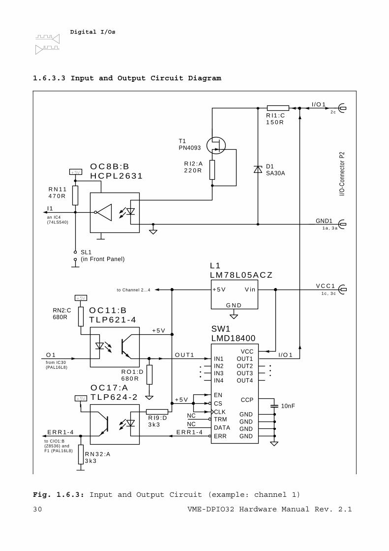
1.6.3.3 Input and Output Circuit Diagram
Fig. 1.6.3: Input and Output Circuit (example: channel 1)
I /O 1
O C 8 B:BH C PL2 631
I/O-C
onne
ctor
P2
2 c
an IC4(74LS540)
R N 1 14 7 0 R
T1PN4093
R I2 :A2 2 0 R
I1
GND11 a , 3 a
D1SA30A
R I1 :C1 5 0 R
SW1LMD18400
NC
E R R 1 -4
O U T1
IN4IN3IN2IN1
TRM
ENCS
DATAERR
OUT4OUT3OUT2OUT1
CCP
GND
VCC
GNDGNDGND
CLK
I/O 1
V C C 11c , 3 c
R I9 :D3 k3
10nF
NC
+ 5 V
E R R 1 -4
R O 1 :D6 8 0 R
+ 5 V
O 1
RN2:C680R
O C 1 1 :BT L P 62 1 -4
O C 1 7 :AT L P 62 4 -2
R N 3 2 :A3 k 3
SL1(in Front Panel)
from IC30(PAL16L8)
to CIO1:B(Z8536) andF1 (PAL16L8)
L1LM 78 L0 5AC Z
V in+ 5 V
G N D
to Channel 2...4
VME-DPIO32 Hardware Manual Rev. 2.130
Connector Pin Assigment
2. Appendix
2.1 Connector Pin Assigments
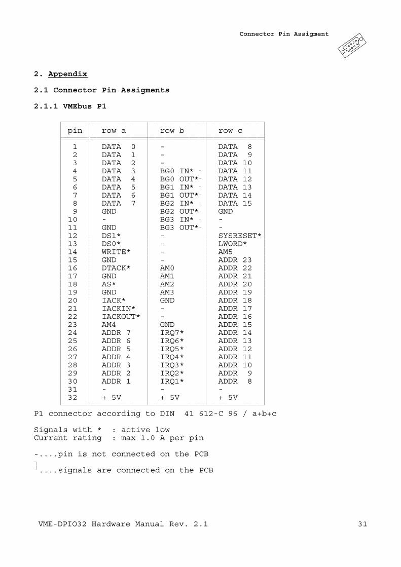
2.1.1 VMEbus P1
pin row a row b row c
1 DATA 0 - DATA 82 DATA 1 - DATA 93 DATA 2 - DATA 104 DATA 3 BG0 IN* DATA 115 DATA 4 BG0 OUT* DATA 126 DATA 5 BG1 IN* DATA 137 DATA 6 BG1 OUT* DATA 148 DATA 7 BG2 IN* DATA 159 GND BG2 OUT* GND
10 - BG3 IN* -11 GND BG3 OUT* -12 DS1* - SYSRESET*13 DS0* - LWORD*14 WRITE* - AM515 GND - ADDR 2316 DTACK* AM0 ADDR 2217 GND AM1 ADDR 2118 AS* AM2 ADDR 2019 GND AM3 ADDR 1920 IACK* GND ADDR 1821 IACKIN* - ADDR 1722 IACKOUT* - ADDR 1623 AM4 GND ADDR 1524 ADDR 7 IRQ7* ADDR 1425 ADDR 6 IRQ6* ADDR 1326 ADDR 5 IRQ5* ADDR 1227 ADDR 4 IRQ4* ADDR 1128 ADDR 3 IRQ3* ADDR 1029 ADDR 2 IRQ2* ADDR 930 ADDR 1 IRQ1* ADDR 831 - - -32 + 5V + 5V + 5V
P1 connector according to DIN 41 612-C 96 / a+b+c
Signals with * : active lowCurrent rating : max 1.0 A per pin
-....pin is not connected on the PCB
....signals are connected on the PCB
VME-DPIO32 Hardware Manual Rev. 2.1 31
Connector Pin Assigment
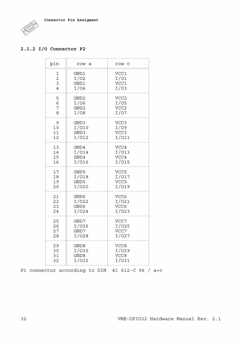
2.1.2 I/O Connector P2
pin row a row c
1 GND1 VCC12 I/O2 I/O13 GND1 VCC14 I/O4 I/O3
5 GND2 VCC26 I/O6 I/O57 GND2 VCC28 I/O8 I/O7
9 GND3 VCC310 I/O10 I/O911 GND3 VCC312 I/O12 I/O11
13 GND4 VCC414 I/O14 I/O1315 GND4 VCC416 I/O16 I/O15
17 GND5 VCC518 I/O18 I/O1719 GND5 VCC520 I/O20 I/O19
21 GND6 VCC622 I/O22 I/O2123 GND6 VCC624 I/O24 I/O23
25 GND7 VCC726 I/O26 I/O2527 GND7 VCC728 I/O28 I/O27
29 GND8 VCC830 I/O30 I/O2931 GND8 VCC832 I/O32 I/O31
P1 connector according to DIN 41 612-C 96 / a+c
VME-DPIO32 Hardware Manual Rev. 2.132
Connector Pin Assigment
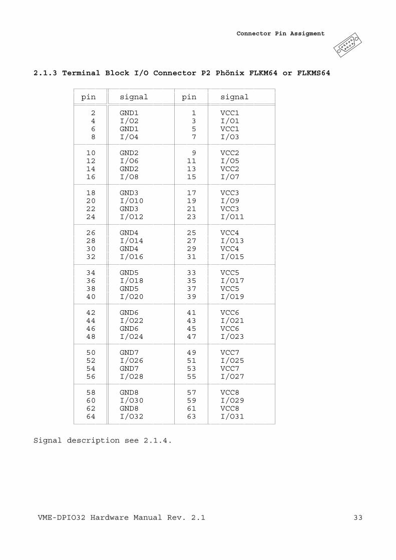
2.1.3 Terminal Block I/O Connector P2 Phönix FLKM64 or FLKMS64
pin signal pin signal
2 GND1 1 VCC14 I/O2 3 I/O16 GND1 5 VCC18 I/O4 7 I/O3
10 GND2 9 VCC212 I/O6 11 I/O514 GND2 13 VCC216 I/O8 15 I/O7
18 GND3 17 VCC320 I/O10 19 I/O922 GND3 21 VCC324 I/O12 23 I/O11
26 GND4 25 VCC428 I/O14 27 I/O1330 GND4 29 VCC432 I/O16 31 I/O15
34 GND5 33 VCC536 I/O18 35 I/O1738 GND5 37 VCC540 I/O20 39 I/O19
42 GND6 41 VCC644 I/O22 43 I/O2146 GND6 45 VCC648 I/O24 47 I/O23
50 GND7 49 VCC752 I/O26 51 I/O2554 GND7 53 VCC756 I/O28 55 I/O27
58 GND8 57 VCC860 I/O30 59 I/O2962 GND8 61 VCC864 I/O32 63 I/O31
Signal description see 2.1.4.
VME-DPIO32 Hardware Manual Rev. 2.1 33
Connector Pin Assigment
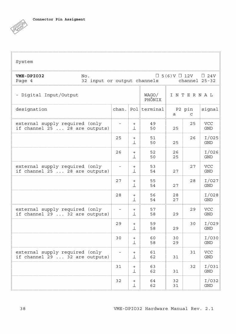
2.1.4 Description of the Signals at the I/O Connector P2(or Terminal Block)
GNDx, VCCx.......power supply (Uvcc) for the digital I/O circuits tobe fed externally. Each 4 channels are locallyconnected to the same power supply (x = 1, 2,...,8)
I/Ox.............I/O channels of VME-DPIO32.(x = 1, 2, ..., 32)
VME-DPIO32 Hardware Manual Rev. 2.134
Connector Pin Assigment
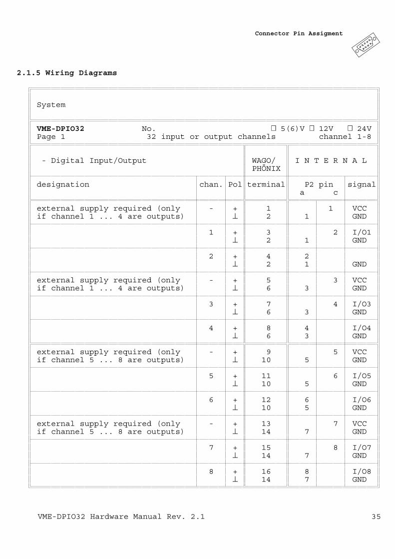
2.1.5 Wiring Diagrams
System
VME-DPIO32 No. 5(6)V 12V 24VPage 1 32 input or output channels channel 1-8
- Digital Input/Output WAGO/ I N T E R N A LPHÖNIX
designation chan. Pol terminal P2 pin signala c
external supply required (only - + 1 1 VCCif channel 1 ... 4 are outputs) ⊥ 2 1 GND
1 + 3 2 I/O1⊥ 2 1 GND
2 + 4 2⊥ 2 1 GND
external supply required (only - + 5 3 VCCif channel 1 ... 4 are outputs) ⊥ 6 3 GND
3 + 7 4 I/O3⊥ 6 3 GND
4 + 8 4 I/O4⊥ 6 3 GND
external supply required (only - + 9 5 VCCif channel 5 ... 8 are outputs) ⊥ 10 5 GND
5 + 11 6 I/O5⊥ 10 5 GND
6 + 12 6 I/O6⊥ 10 5 GND
external supply required (only - + 13 7 VCCif channel 5 ... 8 are outputs) ⊥ 14 7 GND
7 + 15 8 I/O7⊥ 14 7 GND
8 + 16 8 I/O8⊥ 14 7 GND
VME-DPIO32 Hardware Manual Rev. 2.1 35
Connector Pin Assigment
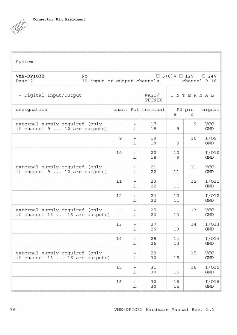
System
VME-DPIO32 No. 5(6)V 12V 24VPage 2 32 input or output channels channel 9-16
- Digital Input/Output WAGO/ I N T E R N A LPHÖNIX
designation chan. Pol terminal P2 pin signala c
external supply required (only - + 17 9 VCCif channel 9 ... 12 are outputs) ⊥ 18 9 GND
9 + 19 10 I/O9⊥ 18 9 GND
10 + 20 10 I/O10⊥ 18 9 GND
external supply required (only - + 21 11 VCCif channel 9 ... 12 are outputs) ⊥ 22 11 GND
11 + 23 12 I/O11⊥ 22 11 GND
12 + 24 12 I/O12⊥ 22 11 GND
external supply required (only - + 25 13 VCCif channel 13 ... 16 are outputs) ⊥ 26 13 GND
13 + 27 14 I/O13⊥ 26 13 GND
14 + 28 14 I/O14⊥ 26 13 GND
external supply required (only - + 29 15 VCCif channel 13 ... 16 are outputs) ⊥ 30 15 GND
15 + 31 16 I/O15⊥ 30 15 GND
16 + 32 16 I/O16⊥ 30 15 GND
VME-DPIO32 Hardware Manual Rev. 2.136
Connector Pin Assigment
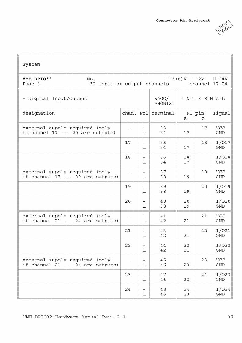
System
VME-DPIO32 No. 5(6)V 12V 24VPage 3 32 input or output channels channel 17-24
- Digital Input/Output WAGO/ I N T E R N A LPHÖNIX
designation chan. Pol terminal P2 pin signala c
external supply required (only - + 33 17 VCCif channel 17 ... 20 are outputs) ⊥ 34 17 GND
17 + 35 18 I/O17⊥ 34 17 GND
18 + 36 18 I/O18⊥ 34 17 GND
external supply required (only - + 37 19 VCCif channel 17 ... 20 are outputs) ⊥ 38 19 GND
19 + 39 20 I/O19⊥ 38 19 GND
20 + 40 20 I/O20⊥ 38 19 GND
external supply required (only - + 41 21 VCCif channel 21 ... 24 are outputs) ⊥ 42 21 GND
21 + 43 22 I/O21⊥ 42 21 GND
22 + 44 22 I/O22⊥ 42 21 GND
external supply required (only - + 45 23 VCCif channel 21 ... 24 are outputs) ⊥ 46 23 GND
23 + 47 24 I/O23⊥ 46 23 GND
24 + 48 24 I/O24⊥ 46 23 GND
VME-DPIO32 Hardware Manual Rev. 2.1 37
Connector Pin Assigment
System
VME-DPIO32 No. 5(6)V 12V 24VPage 4 32 input or output channels channel 25-32
- Digital Input/Output WAGO/ I N T E R N A LPHÖNIX
designation chan. Pol terminal P2 pin signala c
external supply required (only - + 49 25 VCCif channel 25 ... 28 are outputs) ⊥ 50 25 GND
25 + 51 26 I/O25⊥ 50 25 GND
26 + 52 26 I/O26⊥ 50 25 GND
external supply required (only - + 53 27 VCCif channel 25 ... 28 are outputs) ⊥ 54 27 GND
27 + 55 28 I/O27⊥ 54 27 GND
28 + 56 28 I/O28⊥ 54 27 GND
external supply required (only - + 57 29 VCCif channel 29 ... 32 are outputs) ⊥ 58 29 GND
29 + 59 30 I/O29⊥ 58 29 GND
30 + 60 30 I/O30⊥ 58 29 GND
external supply required (only - + 61 31 VCCif channel 29 ... 32 are outputs) ⊥ 62 31 GND
31 + 63 32 I/O31⊥ 62 31 GND
32 + 64 32 I/O32⊥ 62 31 GND
VME-DPIO32 Hardware Manual Rev. 2.138
Front Panel
2.2 Front Panel
VME-DPIO32 Hardware Manual Rev. 2.1 39

VME-DPIO32 Hardware Manual Rev. 2.140
Circuit Diagrams
2.3 Circuit Diagrams
VME-DPIO32 Hardware Manual Rev. 2.1 41

VME-DPIO32 Hardware Manual Rev. 2.142
Data Sheets
2.4 Data Sheets
LMD18400
CIO Z8536
HD63143
VME-DPIO32 Hardware Manual Rev. 2.1 43