Embed Size (px)
Citation preview
8/10/2019 Sicard Slides
http://slidepdf.com/reader/full/sicard-slides 1/21
1
TEACHING CMOS CIRCUIT DESIGN IN NANOSCALETECHNOLOGIES USING MICROWIND
Etienne Sicard Sonia Ben DhiaDepartment of Electrical & ComputerEngineeringINSA – University of ToulouseFrancee-mail:[email protected] [email protected]
Syed Mahfuzul Aziz
School of Electrical &Information EngineeringUniversity of South Australia Australiae-mail:[email protected]
8/10/2019 Sicard Slides
http://slidepdf.com/reader/full/sicard-slides 2/21
2
1. CONTEXT
2. EDUCATIONAL NEEDS
3. MICROWIND
4. EVALUATION
5. PRESPECTIVES
7. CONCLUSION
SUMMARY
8/10/2019 Sicard Slides
http://slidepdf.com/reader/full/sicard-slides 3/21
3
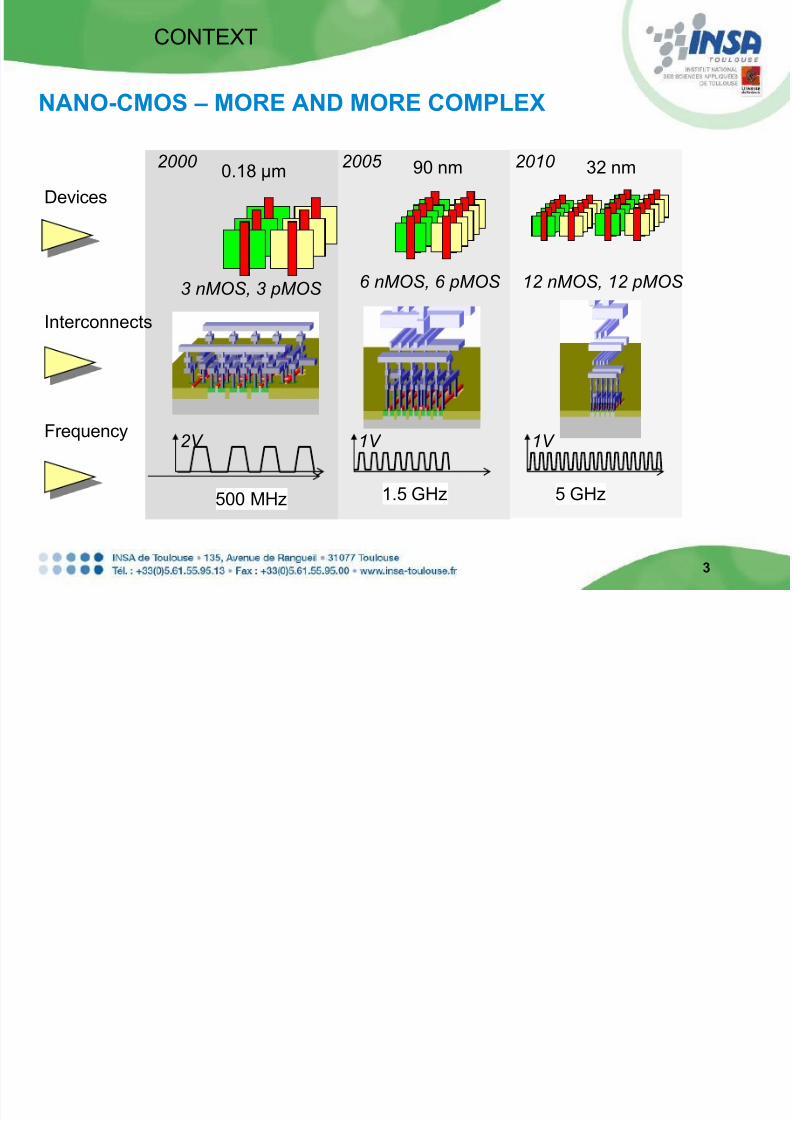
0.18 µm2000
500 MHz
Devices
Interconnects
Frequency2V
3 nMOS, 3 pMOS
CONTEXT
NANO-CMOS – MORE AND MORE COMPLEX
2005 90 nm
1.5 GHz
1V
6 nMOS, 6 pMOS
2010 32 nm
5 GHz
1V
12 nMOS, 12 pMOS
8/10/2019 Sicard Slides
http://slidepdf.com/reader/full/sicard-slides 4/214
CONTEXT
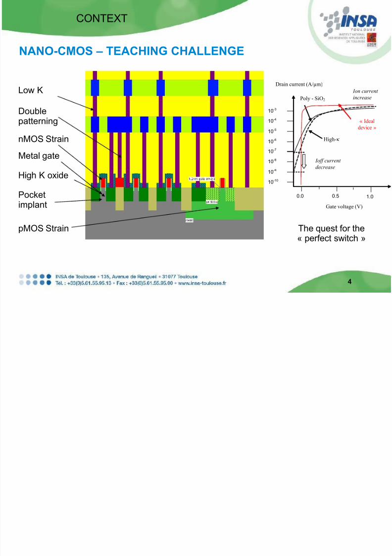
NANO-CMOS – TEACHING CHALLENGE
Low K
Doublepatterning
Metal gate
nMOS Strain
implant
pMOS Strain
High K oxide10-10
10-9
10-8
10-7
10-6
10-5
10-4
10-3
0.0 0.5 1.0
Poly - SiO2
High-
Gate voltage (V)
Drain current (A/µm)
Ioff current
decrease
Ion current
increase
« Ideal
device »
The quest for the« perfect switch »
8/10/2019 Sicard Slides
http://slidepdf.com/reader/full/sicard-slides 5/21
5
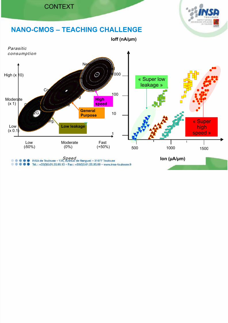
CONTEXT
NANO-CMOS – TEACHING CHALLENGE
Parasit ic
consumpt ion
High (x 10)
Moderate(x 1)
Low(x 0.1)
Speed
Fast(+50%)
Moderate(0%)
Low(-50%)
High- end
servers
Servers
Networking
Computing
MobileComputing
Consumer
3G phones
2G phones
MP3
Digital camera
Highspeed
GeneralPurpose
Low leakage
Personal org.
1
10
100
1000
500 1000 1500
Ion (µA/µm)
Ioff (nA/µm)
« Superhigh
speed »
« Super lowleakage »
8/10/2019 Sicard Slides
http://slidepdf.com/reader/full/sicard-slides 6/21
6
CONTEXT
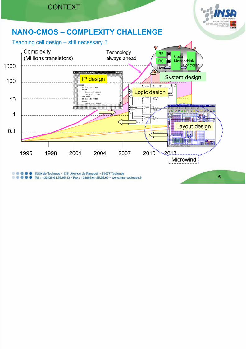
1995 1998 2001 2004 2007 2010
Complexity
(Millions transistors)
0.1
1
10
100
1000
Logic design
Layout design
IP design
Link
Controller
RF
RS
Host
Interface
Code
Manager
System design
Technology
always ahead
2013Microwind
NANO-CMOS – COMPLEXITY CHALLENGE
Teaching cell design – still necessary ?
8/10/2019 Sicard Slides
http://slidepdf.com/reader/full/sicard-slides 7/21
7
EDUCATIONAL NEEDS
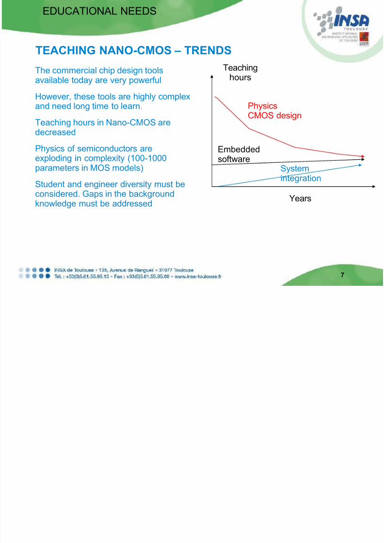
The commercial chip design toolsavailable today are very powerful
However, these tools are highly complexand need long time to learn.
Teaching hours in Nano-CMOS are
decreased
Physics of semiconductors areexploding in complexity (100-1000parameters in MOS models)
Student and engineer diversity must beconsidered. Gaps in the background
knowledge must be addressed
TEACHING NANO-CMOS – TRENDS
PhysicsCMOS design
Teachinghours
Systemintegration
Years
Embeddedsoftware
8/10/2019 Sicard Slides
http://slidepdf.com/reader/full/sicard-slides 8/21
8
EDUCATIONAL NEEDS
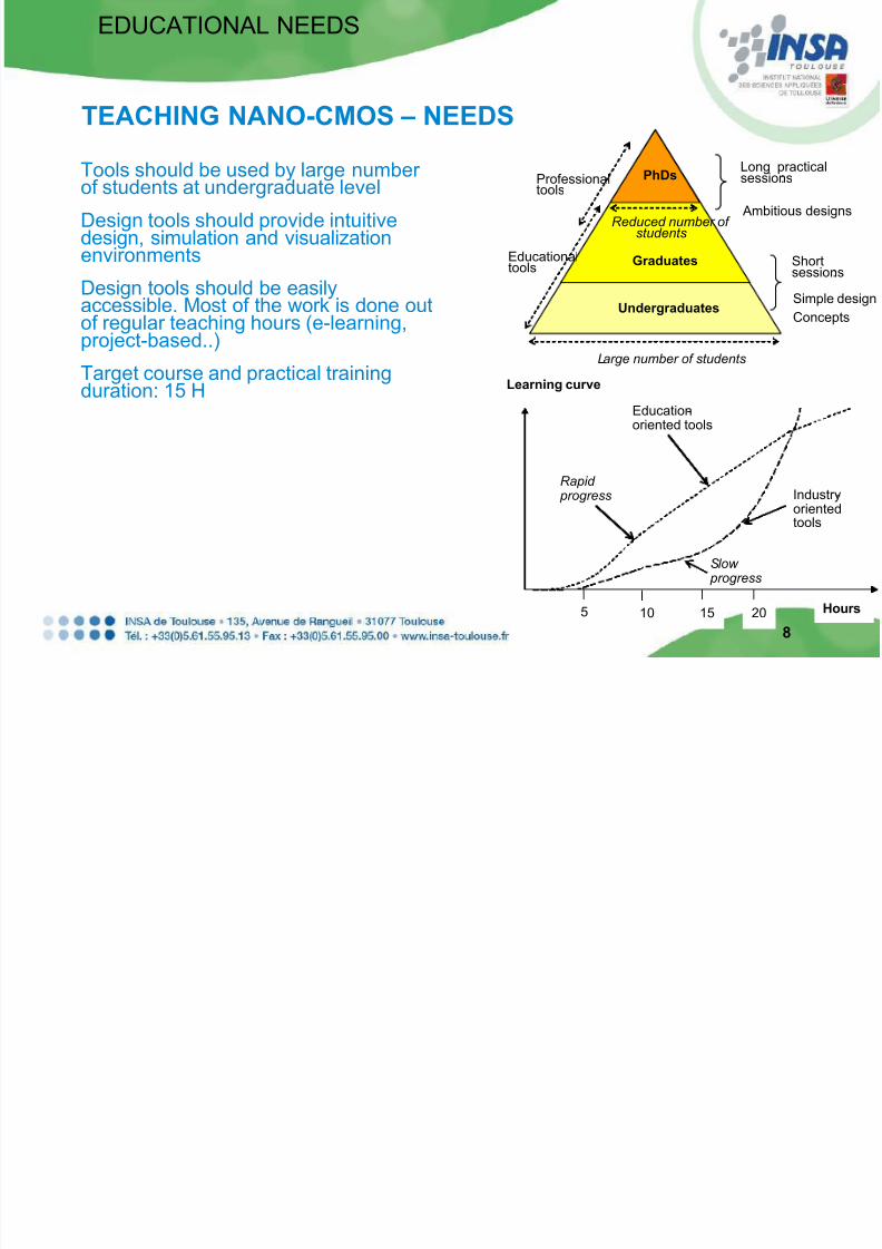
Tools should be used by large numberof students at undergraduate level
Design tools should provide intuitivedesign, simulation and visualizationenvironments
Design tools should be easily
accessible. Most of the work is done outof regular teaching hours (e-learning,project-based..)
Target course and practical trainingduration: 15 H
TEACHING NANO-CMOS – NEEDS
Professionaltools
Graduates
Undergraduates
PhDs
Educationaltools
Shortsessions:
Simple design
Concepts
Long practicalsessions:
Ambitious designs
L arge number of students
Reduced number ofstudents
Learning curve
Hours
Industry-orientedtools
Education-oriented tools
Rapid progress
5 10 15 20
S low progress
8/10/2019 Sicard Slides
http://slidepdf.com/reader/full/sicard-slides 9/21
9
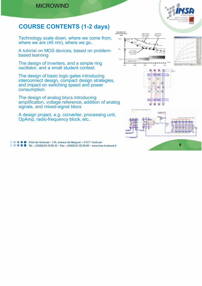
MICROWIND
Technology scale down, where we come from,where we are (45 nm), where we go..
A tutorial on MOS devices, based on problem-based learning
The design of inverters, and a simple ringoscillator, and a small student contest.
The design of basic logic gates introducinginterconnect design, compact design strategies,and impact on switching speed and powerconsumption.
The design of analog blocs introducingamplification, voltage reference, addition of analog
signals, and mixed-signal blocs
A design project, e.g. converter, processing unit,OpAmp, radio-frequency block, etc..
COURSE CONTENTS (1-2 days)
1995 2000 2005 2010 2015
0.1nm
1nm
10nm
Equivalent Gate
Dielectric Thickness
(nm)
Year
0.25 m
0.18 m
0.13 m
90nm65nm
High voltage
MOS (doublegate oxide)
Technology
addressed in2010
22nmLow voltage
MOS (minimum
gate oxide)
SiO2 (r =3.9)
SiON (r =4.2-6.5)
HighK (r =7-20)
45nm 32nm
18nm 11nm
8/10/2019 Sicard Slides
http://slidepdf.com/reader/full/sicard-slides 10/21
10
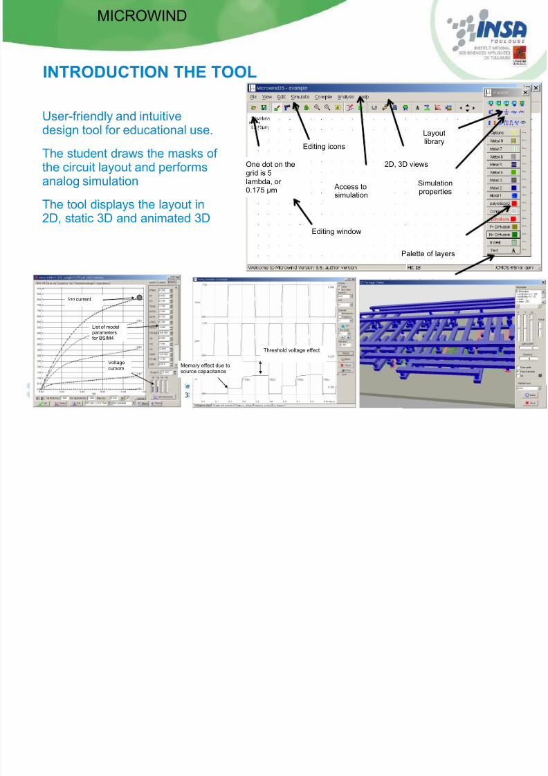
MICROWIND
User-friendly and intuitivedesign tool for educational use.
The student draws the masks ofthe circuit layout and performsanalog simulation
The tool displays the layout in2D, static 3D and animated 3D
Editing window
One dot on thegrid is 5lambda, or
0.175 µm
Editing icons
Access to
simulation
2D, 3D views
Simulation
properties
Layoutlibrary
Active technology
Palette of layers
INTRODUCTION THE TOOL
Ion current
Voltagecursors
List of modelparametersfor BSIM4
Memory effect due tosource capacitance
Threshold voltage effect
8/10/2019 Sicard Slides
http://slidepdf.com/reader/full/sicard-slides 11/21
8/10/2019 Sicard Slides
http://slidepdf.com/reader/full/sicard-slides 12/21
12
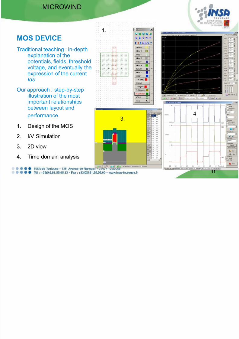
MICROWIND
BASIC GATE DESIGN
Illustration of the most importantrelationships between layout
and performance.
1. Design of pMOS
2. Design of inverters
3. Design of a VCO
4. Try to optimize the VCO forhighest possible speed
5. Improve MOS size
6. Change MOS options
7. Make the layout morecompact
8. Keep an eye on powerconsumption
1.2.
3.
4.
8/10/2019 Sicard Slides
http://slidepdf.com/reader/full/sicard-slides 13/21
13
MICROWIND
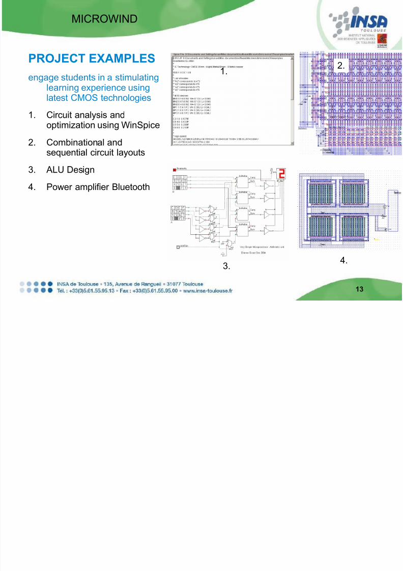
PROJECT EXAMPLES
engage students in a stimulatinglearning experience usinglatest CMOS technologies
1. Circuit analysis andoptimization using WinSpice
2. Combinational andsequential circuit layouts
3. ALU Design
4. Power amplifier Bluetooth
1.2.
3.4.
EVALUATION
8/10/2019 Sicard Slides
http://slidepdf.com/reader/full/sicard-slides 14/21
14
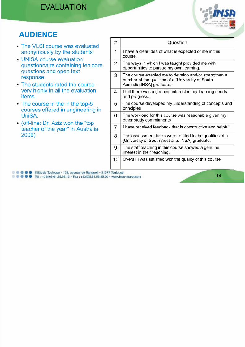
EVALUATION
• The VLSI course was evaluatedanonymously by the students
• UNISA course evaluationquestionnaire containing ten corequestions and open textresponse.
•
The students rated the coursevery highly in all the evaluationitems.
• The course in the in the top-5courses offered in engineering inUniSA.
• (off-line: Dr. Aziz won the “top
teacher of the year” in Australia2009)
AUDIENCE
# Question1 I have a clear idea of what is expected of me in this
course.
2 The ways in which I was taught provided me withopportunities to pursue my own learning.
3 The course enabled me to develop and/or strengthen anumber of the qualities of a [University of South
Australia,INSA] graduate.4 I felt there was a genuine interest in my learning needs
and progress.
5 The course developed my understanding of concepts andprinciples
6 The workload for this course was reasonable given myother study commitments
7I have received feedback that is constructive and helpful.
8 The assessment tasks were related to the qualities of a[University of South Australia, INSA] graduate.
9 The staff teaching in this course showed a genuineinterest in their teaching.
10 Overall I was satisfied with the quality of this course
EVALUATION
8/10/2019 Sicard Slides
http://slidepdf.com/reader/full/sicard-slides 15/21
15
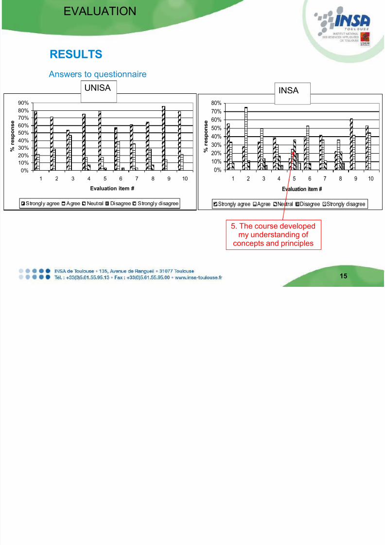
EVALUATION
Answers to questionnaire
RESULTS
0%
10%
20%
30%
40%
50%
60%
70%
80%
90%
1 2 3 4 5 6 7 8 9 10
Evaluation item #
% r
e s p
o n s e
Strongly agree Agree Neutral Disagree Strongly disagree
UNISA
0%
10%
20%
30%40%
50%
60%
70%
80%
1 2 3 4 5 6 7 8 9 10
Evaluation item #
% r e s p
o n s e
Strongly agree Agree Neutral Disagree Strongly disagree
5. The course developedmy understanding of
concepts and principles
INSA
EVALUATION
8/10/2019 Sicard Slides
http://slidepdf.com/reader/full/sicard-slides 16/21
16
EVALUATION
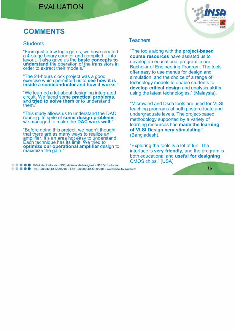
“From just a few logic gates, we have createda 4-stage binary counter and compiled it intolayout. It also gave us the basic concepts tounderstand the operation of the transistors inorder to extract their models.”
“The 24-hours clock project was a goodexercise which permitted us to see how it isinside a semiconductor and how it works.”
“We learned a lot about designing integratedcircuit. We faced some practical problems,and tried to solve them or to understandthem.”
“This study allows us to understand the DACrunning. In spite of some design problems,we managed to make the DAC work well.”
“Before doing this project, we hadn’t thoughtthat there are as many ways to realize anamplifier. It’s an area not easy to understand.Each technique has its limit. We tried tooptimize our operational amplifier design tomaximize the gain.”
COMMENTS
Students
“The tools along with the project-basedcourse resources have assisted us todevelop an educational program in ourBachelor of Engineering Program. The toolsoffer easy to use menus for design andsimulation, and the choice of a range of
technology models to enable students todevelop critical design and analysis skills using the latest technologies.” (Malaysia).
“Microwind and Dsch tools are used for VLSIteaching programs at both postgraduate andundergraduate levels. The project-basedmethodology supported by a variety of
learning resources has made the learningof VLSI Design very stimulating.”(Bangladesh).
“Exploring the tools is a lot of fun. Theinterface is very friendly, and the program isboth educational and useful for designing CMOS chips.” (USA)
Teachers
8/10/2019 Sicard Slides
http://slidepdf.com/reader/full/sicard-slides 17/21
17
PERSPECTIVES
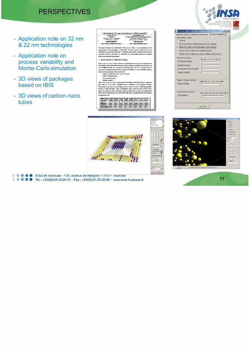
• Application note on 32 nm
& 22 nm technologies
• Application note onprocess variability andMonte-Carlo simulation
• 3D views of packagesbased on IBIS
• 3D views of carbon-nanotubes
8/10/2019 Sicard Slides
http://slidepdf.com/reader/full/sicard-slides 18/21
18
Intuitive and user friendly design tools enabled students to develop circuit
design skills using nano-CMOS technologies
Illustrations (2D, 3D, I/V) help to handle increased process complexity and
refinements
Effective project-based learning methodologies, helping to understand the
impacts of technology scale down on factors such as speed, power and
noise.
Digital and analog basic bloc design with high levels of student satisfaction.
Projects stimulate student curiosity and thinking.
Software to be tuned to 22, 17 and 11 nm technologies
Novel devices to be introduced when appropriate
CONCLUSION
REFERENCES
8/10/2019 Sicard Slides
http://slidepdf.com/reader/full/sicard-slides 19/21
19
[1] E. Sicard and S. Ben Dhia “Basic CMOS CellDesign” McGraw Hill professional series, 2006. [2] E. Sicard and S. Ben Dhia “Advanced CMOS
Cell Design” McGraw-Hill professional series, 2007.[3] E. Sicard, “Microwind & Dsch User's Manual,
Version 3.5”, June 2009. Online at
www.microwind.org.[4] S. M. Aziz, E. Sicard, S. Ben Dhia “Effective
Teaching in Physical Design of Integrated Circuitsusing Educational Tools” to appear IEEE TransEducation, 2010
REFERENCES
The tool, manual and course
slides are online at
www.microwind.org
REFERENCES
8/10/2019 Sicard Slides
http://slidepdf.com/reader/full/sicard-slides 20/21
20
REFERENCES
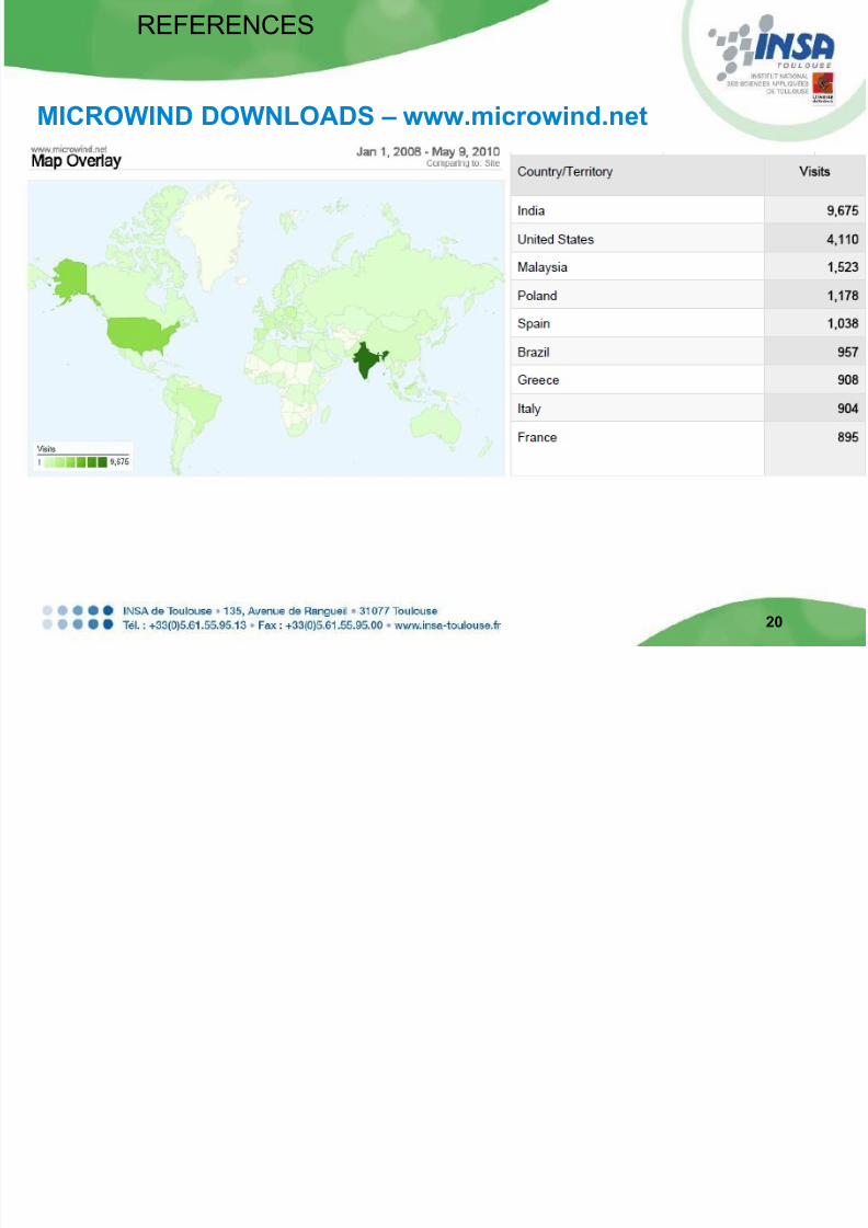
MICROWIND DOWNLOADS – www.microwind.net
8/10/2019 Sicard Slides
http://slidepdf.com/reader/full/sicard-slides 21/21
21
THANK YOU FOR YOUR ATTENTION