Embed Size (px)
Citation preview
MICROWIND APPLICATION NOTE 45 nm technology
Page 1/16 [email protected] 27/06/07
Introducing 45 nm technology in Microwind3 Etienne SICARD
Professor INSA-Dgei, 135 Av de Rangueil
31077 Toulouse – France www.microwind.org
email: [email protected]
Syed Mahfuzul Aziz School of Electrical & Information Engineering
University of South Australia Mawson Lakes, SA 5095, Australia
www.unisa.edu.au
email: [email protected]
This paper describes the improvements related to the CMOS 45 nm technology and the
implementation of this technology in Microwind3. The main novelties related to the 45 nm technology
such as the high-k gate oxide, metal-gate and very low-K interconnect dielectric is described. The
performances of a ring oscillator layout and a 6-transistor RAM memory layout are also analyzed.
1. Recent trends in CMOS technology
Firstly, we give an overview of the evolution of important parameters such as the integrated circuit
(IC) complexity, gate length, switching delay and supply voltage with a prospective vision down to the
22 nm CMOS technology. The trend of CMOS technology improvement continues to be driven by the
need to integrate more functions within a given silicon area. Table 1 gives an overview of the key
parameters for technological nodes from 180 nm, introduced in 1999, down to 22 nm, which is
supposed to be in production around 2011. Demonstration chips using 45-nm technology have been
reported starting in 2004. Mass market manufacturing with this technology is scheduled for late 2007.
Technology node 130 nm 90 nm 65 nm 45 nm 32 nm 22 nm First production 2001 2003 2005 2007 2009 2011 Effective gate length
70 nm 50 nm 35 nm 25 nm 17 nm 12 nm
Gate material Poly
Poly
Poly
Metal
Metal
Metal
Gate dielectric SiO2 SiO2 SiON High K High K High K Kgates/mm2 240 480 900 1500 2800 4500 Memory point (µ2) 2.4 1.3 0.6 0.3 0.15 0.08
Table 1: Technological evolution and forecast up to 2011
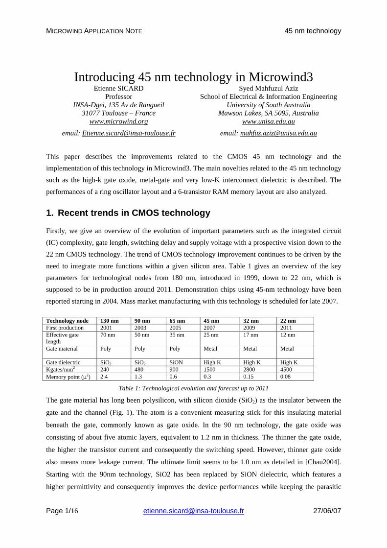
The gate material has long been polysilicon, with silicon dioxide (SiO2) as the insulator between the
gate and the channel (Fig. 1). The atom is a convenient measuring stick for this insulating material
beneath the gate, commonly known as gate oxide. In the 90 nm technology, the gate oxide was
consisting of about five atomic layers, equivalent to 1.2 nm in thickness. The thinner the gate oxide,
the higher the transistor current and consequently the switching speed. However, thinner gate oxide
also means more leakage current. The ultimate limit seems to be 1.0 nm as detailed in [Chau2004].
Starting with the 90nm technology, SiO2 has been replaced by SiON dielectric, which features a
higher permittivity and consequently improves the device performances while keeping the parasitic
MICROWIND APPLICATION NOTE 45 nm technology
Page 2/16 [email protected] 27/06/07
leakage current within reasonable limits. Starting with the 45-nm technology, leakage reduction has
been achieved through the use of various high-K dielectrics such as Hafnium Oxide HfO2 (εr=12),
Zyrconium Oxide ZrO2 (εr=20), Tantalum Oxide Ta2O5 (εr=25) or Titanium Oxide TiO2 (εr=40). This
provides much higher device performance as if the device was fabricated in a technology using
conventional SiO2 with much reduced “equivalent SiO2 thickness”.
1995 2000 2005 2010 2015
0.1nm
1nm
10nm
Gate Dielectric Thickness (nm)
Year
0.25µm
0.18µm
0.13µm 90nm
65nm
32nm
High voltage MOS (double gate oxide)
Technology addressed in this application note
22nm
Low voltage MOS (minimum
gate oxide)
SiO2 (εr=3.9)
45nm
SiON (εr=4.2-6.5)
HighK (εr=7-20)
Figure 1 : The technology scale down towards nano-scale devices
The High-K dielectric enabled a thinner “equivalent” oxide thickness while keeping leakage current
low. The “equivalent oxide thickness” TOXE is defined by Equ. 1. For the 45-nm technology, the
high-K permittivity declared in the rule file is 10 (Parameter “GateK”). The physical oxide thickness is
3.5 nm, and by applying equ. 1, TOXE is 1.4nm. These parameters are in close agreement with those
in Song’s review on 45-nm gate stacks [Song2006].
= −
−khigh
khigh
SiO tTOXEεε 2 (Equ. 1)
Where
εSiO2 = dielectric permittivity of SiO2 (3.9, no unit)
εhigh-k = High-K dielectric permittivity
thigh-k = High-K oxide thickness (m)
In the 45-nm technology node, some IC manufacturers targeting low cost production have kept the
polysilicon gate and the SiON oxide, while still achieving important speed and power improvements,
thanks to channel length reduction [Fujitsu2005]. However, IC manufacturers oriented towards very
high performances have replaced the SiON oxide by Hafnium Oxide to obtain an equivalent oxide
thickness TOXE close to 1.0 nm.
MICROWIND APPLICATION NOTE 45 nm technology
Page 3/16 [email protected] 27/06/07
At each lithography scaling, the linear dimensions are approximately reduced by a factor of 0.7, and
the areas are reduced by factor of 2. Smaller cell sizes lead to higher integration density which has
risen to nearly 2 million gates per mm2 in the 45-nm technology.
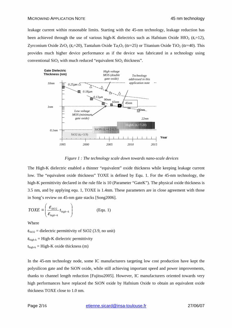
The integrated circuit market has been growing steadily since many years, due to ever-increasing
demand for electronic devices. The production of integrated circuits for various technologies over the
years is illustrated in Fig. 2. It can be seen that a new technology has appeared regularly every two
years, with a ramp up close to three years. The production peak is constantly increased, and similar
trends should be observed for novel technologies such as 45nm (forecast peak in 2010).
1995 2000 2005 2010 2015
Production
Year
0. 5µm
0.18µm
130nm
90nm
65nm
0.35µm
0.25µm
45nm
Figure 2 : Technology ramping every two years introducing the 45 nm technology
Prototype 45-nm processes have been introduced by TSMC in 2004 [Tsmc2004] and Fujitsu in 2005
[Fujitsu2005]. In 2007, Intel announced its 45-nm CMOS industrial process and revealed some key
features about metal gates. The “Common Platform” [Common2007] including IBM, Chartered
Semiconductor, Samsung and Infineon has set-up a 45-nm CMOS technology for commercial
production in 2007. The transistor channels range from 25 nm to 40 nm in size (25 to 40 billionths of a
meter). Some of the key features of the 45 nm technologies from various providers are given in Table
2.
Parameter Value VDD (V) 0.85-1.2 V Effective gate length (nm) 25-40 Ion N (µA/µm) at 1V 750-1000 Ion P (µA/µm) at 1V 350-530 Ioff N (nA/µm) 5-100 Ioff P (nA/µm) 5-100 Gate dielectric SiON, HfO2 Equivalent oxide thickness (nm)
1.1-1.5
# of metal layers 6-10 Interconnect layer permittivity K
2.2-2.6
Table 2: Key features of the 45 nm technology
MICROWIND APPLICATION NOTE 45 nm technology
Page 4/16 [email protected] 27/06/07
Compared to 65-nm technology, most 45-nm technologies offer:
• 30 % increase in switching performance
• 30 % less power consumption
• 2 times higher density
• X 2 reduction of the leakage between source and drain and through the gate oxide
Gate Material
For 40 years, the SiO2 gate oxide combined with polysilicon have been serving as the key enabling
materials for scaling MOS devices down to the 90nm technology node. One of the struggles the IC
manufacturers went through was being able to scale the gate dielectric thickness to match continuous
requirements for improved switching performance. But the leakage current between drain/source and
the gate became significant.
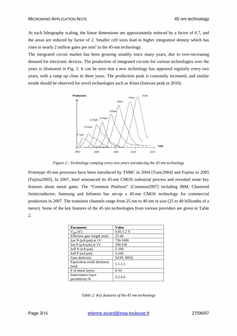
The combination of high dielectric materials with polysilicon gate has revealed [Chau04, Intel]
unexpected increase of parasitic threshold voltage and severe degradation of the carrier mobility,
which jeopardized the benefits of a scaled channel length. For the first time in 40 years of CMOS
manufacturing, the poly gate has been abandoned. Nickel-Silicide (NiSi), Titanium-Nitride (TiN) etc.
are the types of gate materials that provide acceptable threshold voltage and alleviate the mobility
degradation problem (Fig. 3). It is interesting to note that most IC manufacturers do not reveal the
exact structure of the metal gate. In combination with Hafnium Oxide (HfO2, εr=12), the metal/high-k
transistors feature outstanding current switching capabilities together with low leakage. Increased on
current, decreased off current and significantly decreased gate leakage are obtained with this novel
combination.
1.2nm K=3.9
Source
Polysilicon gate
Si02 Gate oxide
Drain
2.0 nm K=12.0
Source
Novel METAL gate (Nickel
Silicide) Hafnium Gate oxide
Drain
Low capacitance (slow device)
High gate leakage 90-nm generation
Equivalent to 0.6 nm SiO2, which means a higher capacitance
(fast device) Reduced gate leakage
Low resistive layer (SiN)
Low resistive layer (SiN)
Figure 3: The metal gate combined with High-K oxide material enhance the MOS device performance in terms of switching speed and significantly reduce the leakage
MICROWIND APPLICATION NOTE 45 nm technology
Page 5/16 [email protected] 27/06/07
10-10
10-9
10-8
10-7
10-6
10-5
10-4
10-3
0.0 0.5 1.0
Poly - SiO2
High-κ
Gate voltage (V)
Drain current (A/µm)
Ioff current decrease
Ion current increase
100
150
200
250
0.0 1.0 2.0
Optimized TiN/HfO2
Equivalent Gate Oxide (nm)
Effective Electron mobility (cm2/V.s)
Poly/HfO2
@ 1 MV/cm
Poly/SiO2
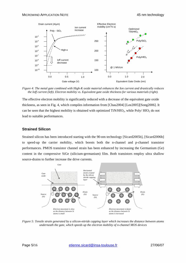
Figure 4: The metal gate combined with High-K oxide material enhances the Ion current and drastically reduces
the Ioff current (left). Electron mobility vs. Equivalent gate oxide thickness for various materials (right).
The effective electron mobility is significantly reduced with a decrease of the equivalent gate oxide
thickness, as seen in Fig. 4, which compiles information from [Chau2004] [Lee2005][Song2006]. It
can be seen that the highest mobility is obtained with optimized TiN/HfO2, while Poly/ HfO2 do not
lead to suitable performances.
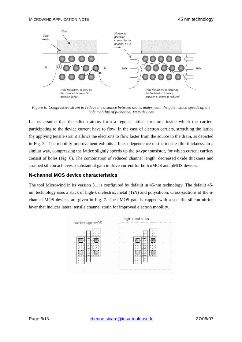
Strained Silicon
Strained silicon has been introduced starting with the 90-nm technology [Sicard2005b], [Sicard2006b]
to speed-up the carrier mobility, which boosts both the n-channel and p-channel transistor
performances. PMOS transistor channel strain has been enhanced by increasing the Germanium (Ge)
content in the compressive SiGe (silicium-germanium) film. Both transistors employ ultra shallow
source-drains to further increase the drive currents.
Electron movement is slow as the distance between Si atoms is small
Electron movement is faster as the distance between Si atoms is increased
Source (Si)
Gate
Gate oxide
Horizontal strain created by the silicon nitride capping layer
Drain (Si)
Drain (Si) Source
(Si)
Figure 5: Tensile strain generated by a silicon-nitride capping layer which increases the distance between atoms underneath the gate, which speeds up the electron mobility of n-channel MOS devices
MICROWIND APPLICATION NOTE 45 nm technology
Page 6/16 [email protected] 27/06/07
Hole movement is slow as the distance between Si atoms is large
Hole movement is faster as the horizontal distance between Si atoms is reduced
SiGe Si Si SiGe
Gate
Gate oxide
Horizontal pressure created by the uniaxial SiGe strain
Figure 6: Compressive strain to reduce the distance between atoms underneath the gate, which speeds up the hole mobility of p-channel MOS devices
Let us assume that the silicon atoms form a regular lattice structure, inside which the carriers
participating to the device current have to flow. In the case of electron carriers, stretching the lattice
(by applying tensile strain) allows the electrons to flow faster from the source to the drain, as depicted
in Fig. 5. The mobility improvement exhibits a linear dependence on the tensile film thickness. In a
similar way, compressing the lattice slightly speeds up the p-type transistor, for which current carriers
consist of holes (Fig. 6). The combination of reduced channel length, decreased oxide thickness and
strained silicon achieves a substantial gain in drive current for both nMOS and pMOS devices.
N-channel MOS device characteristics
The tool Microwind in its version 3.1 is configured by default in 45-nm technology. The default 45-
nm technology uses a stack of high-k dielectric, metal (TiN) and polysilicon. Cross-sections of the n-
channel MOS devices are given in Fig. 7. The nMOS gate is capped with a specific silicon nitride
layer that induces lateral tensile channel strain for improved electron mobility.
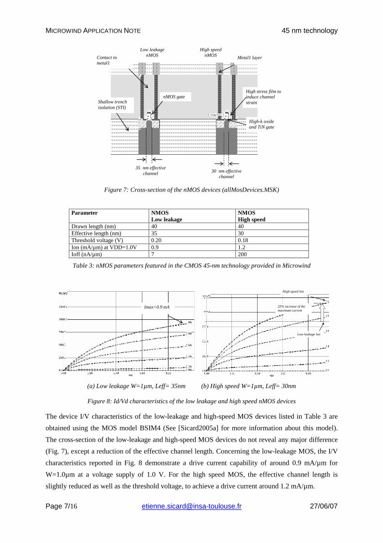
MICROWIND APPLICATION NOTE 45 nm technology
Page 7/16 [email protected] 27/06/07
nMOS gate
Contact to metal1
Metal1 layer
Shallow trench isolation (STI)
35 nm effective channel 30 nm effective
channel
Low leakage nMOS
High speed nMOS
High stress film to induce channel strain
High-k oxide and TiN gate
Figure 7: Cross-section of the nMOS devices (allMosDevices.MSK)
Parameter NMOS
Low leakage NMOS High speed
Drawn length (nm) 40 40 Effective length (nm) 35 30 Threshold voltage (V) 0.20 0.18 Ion (mA/µm) at VDD=1.0V 0.9 1.2 Ioff (nA/µm) 7 200
Table 3: nMOS parameters featured in the CMOS 45-nm technology provided in Microwind
Imax=0.9 mA
25% increase of the maximum current
Low-leakage Ion
High-speed Ion
(a) Low leakage W=1µm, Leff= 35nm (b) High speed W=1µm, Leff= 30nm
Figure 8: Id/Vd characteristics of the low leakage and high speed nMOS devices
The device I/V characteristics of the low-leakage and high-speed MOS devices listed in Table 3 are
obtained using the MOS model BSIM4 (See [Sicard2005a] for more information about this model).
The cross-section of the low-leakage and high-speed MOS devices do not reveal any major difference
(Fig. 7), except a reduction of the effective channel length. Concerning the low-leakage MOS, the I/V
characteristics reported in Fig. 8 demonstrate a drive current capability of around 0.9 mA/µm for
W=1.0µm at a voltage supply of 1.0 V. For the high speed MOS, the effective channel length is
slightly reduced as well as the threshold voltage, to achieve a drive current around 1.2 mA/µm.
MICROWIND APPLICATION NOTE 45 nm technology
Page 8/16 [email protected] 27/06/07
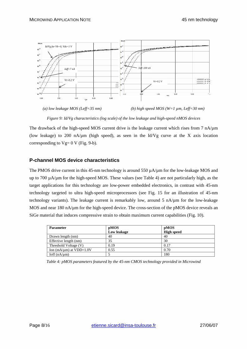
Id/Vg for Vb=0, Vds=1 V
Ioff=7 nA
Vt=0.2 V
Ioff=200 nA
Vt=0.2 V
(a) low leakage MOS (Leff=35 nm) (b) high speed MOS (W=1 µm, Leff=30 nm)
Figure 9: Id/Vg characteristics (log scale) of the low leakage and high-speed nMOS devices
The drawback of the high-speed MOS current drive is the leakage current which rises from 7 nA/µm
(low leakage) to 200 nA/µm (high speed), as seen in the Id/Vg curve at the X axis location
corresponding to Vg= 0 V (Fig. 9-b).
P-channel MOS device characteristics
The PMOS drive current in this 45-nm technology is around 550 µA/µm for the low-leakage MOS and
up to 700 µA/µm for the high-speed MOS. These values (see Table 4) are not particularly high, as the
target applications for this technology are low-power embedded electronics, in contrast with 45-nm
technology targeted to ultra high-speed microprocessors (see Fig. 15 for an illustration of 45-nm
technology variants). The leakage current is remarkably low, around 5 nA/µm for the low-leakage
MOS and near 180 nA/µm for the high-speed device. The cross-section of the pMOS device reveals an
SiGe material that induces compressive strain to obtain maximum current capabilities (Fig. 10).
Parameter pMOS
Low leakage pMOS High speed
Drawn length (nm) 40 40 Effective length (nm) 35 30 Threshold Voltage (V) 0.19 0.17 Ion (mA/µm) at VDD=1.0V 0.55 0.70 Ioff (nA/µm) 5 180
Table 4: pMOS parameters featured by the 45-nm CMOS technology provided in Microwind
MICROWIND APPLICATION NOTE 45 nm technology
Page 9/16 [email protected] 27/06/07
pMOS gate
Contact to metal1
Metal1 layer
Shallow trench isolation (STI)
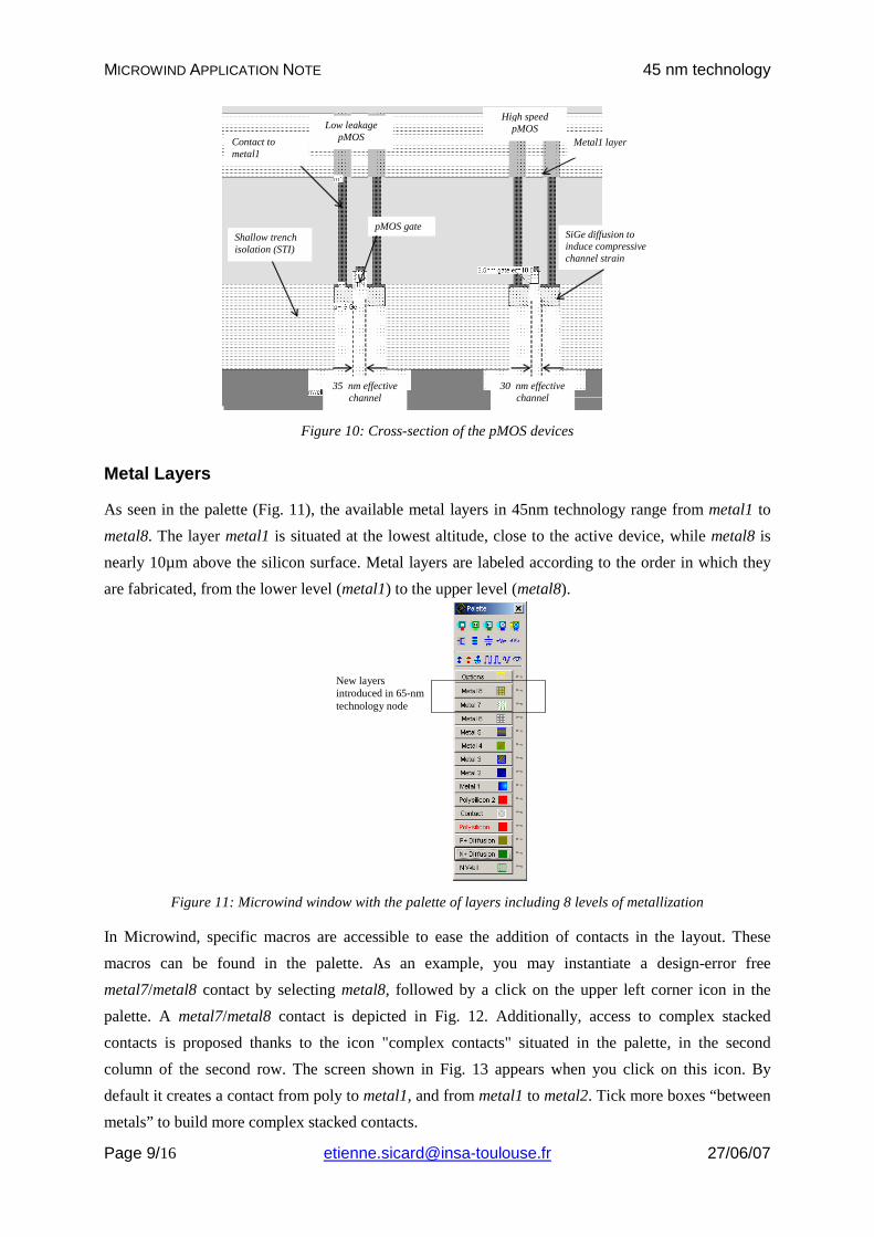
35 nm effective channel
30 nm effective channel
Low leakage pMOS
High speed pMOS
SiGe diffusion to induce compressive channel strain
Figure 10: Cross-section of the pMOS devices
Metal Layers
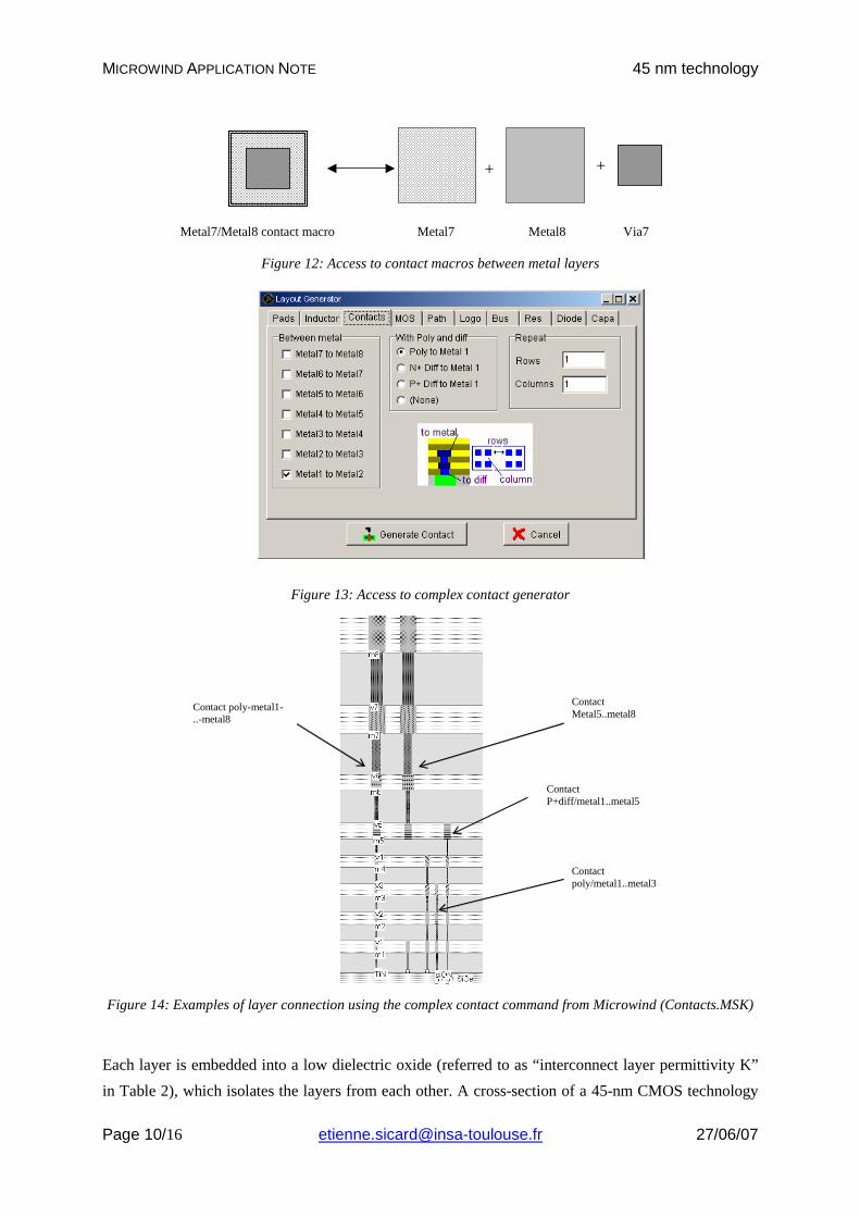
As seen in the palette (Fig. 11), the available metal layers in 45nm technology range from metal1 to
metal8. The layer metal1 is situated at the lowest altitude, close to the active device, while metal8 is
nearly 10µm above the silicon surface. Metal layers are labeled according to the order in which they
are fabricated, from the lower level (metal1) to the upper level (metal8).
New layers introduced in 65-nm technology node
Figure 11: Microwind window with the palette of layers including 8 levels of metallization
In Microwind, specific macros are accessible to ease the addition of contacts in the layout. These
macros can be found in the palette. As an example, you may instantiate a design-error free
metal7/metal8 contact by selecting metal8, followed by a click on the upper left corner icon in the
palette. A metal7/metal8 contact is depicted in Fig. 12. Additionally, access to complex stacked
contacts is proposed thanks to the icon "complex contacts" situated in the palette, in the second
column of the second row. The screen shown in Fig. 13 appears when you click on this icon. By
default it creates a contact from poly to metal1, and from metal1 to metal2. Tick more boxes “between
metals” to build more complex stacked contacts.
MICROWIND APPLICATION NOTE 45 nm technology
Page 10/16 [email protected] 27/06/07
+ +
Metal7/Metal8 contact macro Metal7 Metal8 Via7
Figure 12: Access to contact macros between metal layers
Figure 13: Access to complex contact generator
Contact poly/metal1..metal3
Contact poly-metal1-..-metal8
Contact P+diff/metal1..metal5
Contact Metal5..metal8
Figure 14: Examples of layer connection using the complex contact command from Microwind (Contacts.MSK)
Each layer is embedded into a low dielectric oxide (referred to as “interconnect layer permittivity K”
in Table 2), which isolates the layers from each other. A cross-section of a 45-nm CMOS technology
MICROWIND APPLICATION NOTE 45 nm technology
Page 11/16 [email protected] 27/06/07
is shown in Fig. 14. In 45-nm technology, the layers metal1..metal4 have almost identical
characteristics. Concerning the design rules, the minimum width w of the interconnect is 3 λ. The
minimum spacing is 4 λ. Layers metal5 and metal6 are a little thicker and wider, while layers metal7
and metal8 are significantly thicker and wider, to drive high currents for power supplies. The design
rules for metal8 are 25 λ (0.5µm) width, 25 λ (0.5µm) spacing.
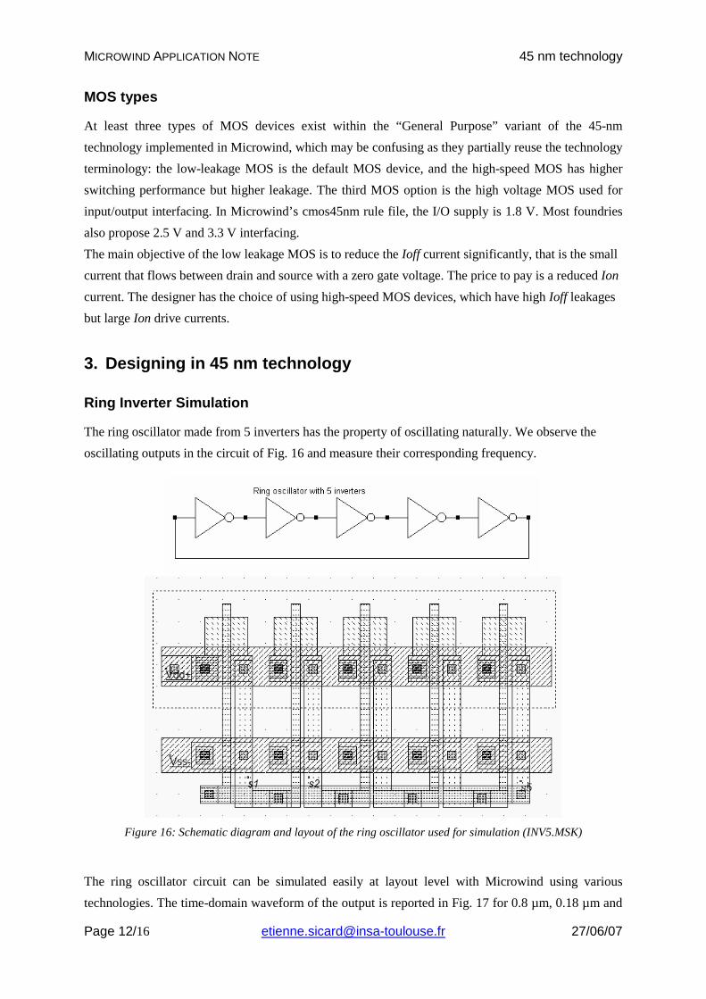
2. 45-nm process variants
There may exist several variants of the 45-nm process technology. One corresponds to the highest
possible speed, at the price of a very high leakage current. This technology is called “High speed” as it
is dedicated to applications for which the highest speed is the primary objective: fast microprocessors,
fast DSP, etc. This technology has not been addressed in Microwind’s 45nm rule file.
The second technological option called “General Purpose” (Fig. 15) is targeted to standard products
where the speed factor is not critical. The leakage current is one order of magnitude lower than for the
high-speed variant, with gate switching decreased by 50%. Only this technology has been
implemented in Microwind.
Parasitic
leakage current
High (x 10)
Moderate (x 1)
Low (x 0.1)
Speed
Fast (+50%)
Moderate (0%)
Low (-50%)
High-end servers
Servers
Networking
Computing
Mobile Computing
Consumer
3G phones
2G phones
MP3
Digital camera
High speed variant
General Purpose variant
Low leakage variant
Microwind 45-nm rule file
Personal org.
Figure 15 : Introducing three variants of the 45-nm technology
There may also exist a third variant called low leakage (bottom left of Fig. 15). This variant concerns
integrated circuits for which the leakage current must remain as low as possible, a criterion that ranks
first in applications such as embedded devices, mobile phones or personal organizers. The operational
voltage is usually from 0.8 V to 1.2 V, depending on the technology variant. In Microwind, we
decided to fix VDD at 1.0 V in the cmos45nm.RUL rule file, which represents a compromise between
all possible technology variations available for this 45-nm node.
MICROWIND APPLICATION NOTE 45 nm technology
Page 12/16 [email protected] 27/06/07
MOS types
At least three types of MOS devices exist within the “General Purpose” variant of the 45-nm
technology implemented in Microwind, which may be confusing as they partially reuse the technology
terminology: the low-leakage MOS is the default MOS device, and the high-speed MOS has higher
switching performance but higher leakage. The third MOS option is the high voltage MOS used for
input/output interfacing. In Microwind’s cmos45nm rule file, the I/O supply is 1.8 V. Most foundries
also propose 2.5 V and 3.3 V interfacing.
The main objective of the low leakage MOS is to reduce the Ioff current significantly, that is the small
current that flows between drain and source with a zero gate voltage. The price to pay is a reduced Ion
current. The designer has the choice of using high-speed MOS devices, which have high Ioff leakages
but large Ion drive currents.
3. Designing in 45 nm technology
Ring Inverter Simulation
The ring oscillator made from 5 inverters has the property of oscillating naturally. We observe the
oscillating outputs in the circuit of Fig. 16 and measure their corresponding frequency.
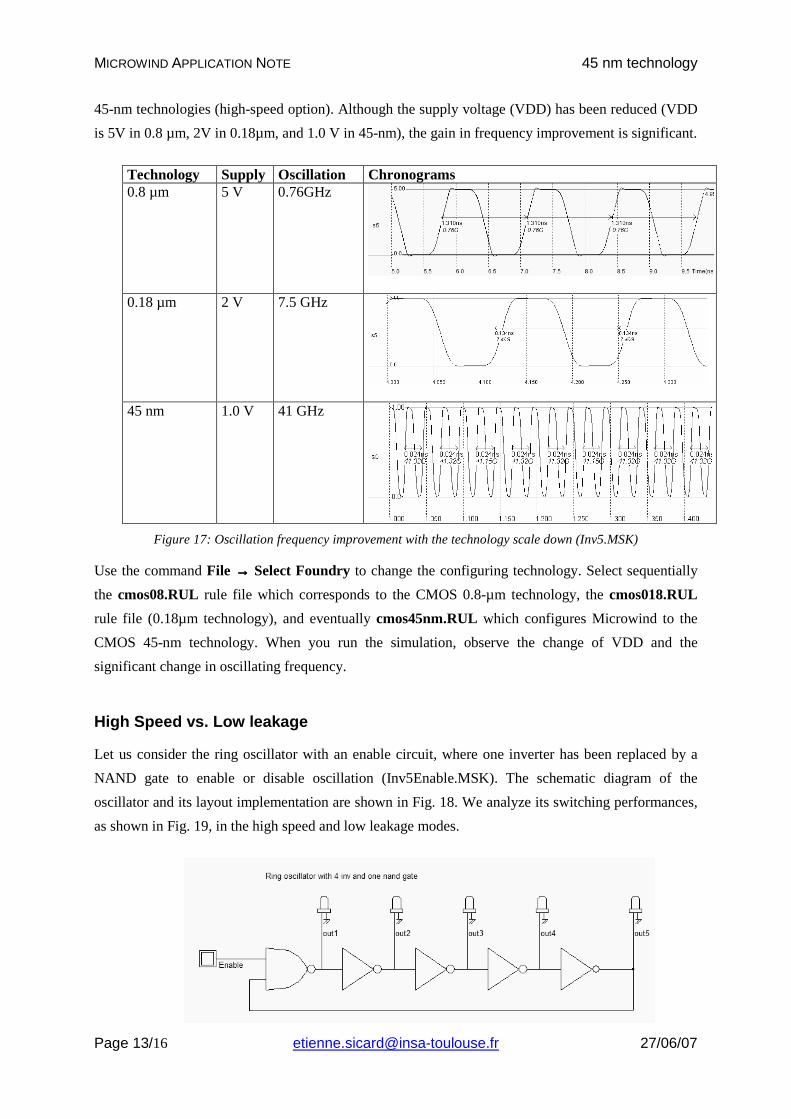
Figure 16: Schematic diagram and layout of the ring oscillator used for simulation (INV5.MSK)
The ring oscillator circuit can be simulated easily at layout level with Microwind using various
technologies. The time-domain waveform of the output is reported in Fig. 17 for 0.8 µm, 0.18 µm and
MICROWIND APPLICATION NOTE 45 nm technology
Page 13/16 [email protected] 27/06/07
45-nm technologies (high-speed option). Although the supply voltage (VDD) has been reduced (VDD
is 5V in 0.8 µm, 2V in 0.18µm, and 1.0 V in 45-nm), the gain in frequency improvement is significant.
Technology Supply Oscillation Chronograms 0.8 µm 5 V 0.76GHz
0.18 µm 2 V 7.5 GHz
45 nm 1.0 V 41 GHz
Figure 17: Oscillation frequency improvement with the technology scale down (Inv5.MSK)
Use the command File →→→→ Select Foundry to change the configuring technology. Select sequentially
the cmos08.RUL rule file which corresponds to the CMOS 0.8-µm technology, the cmos018.RUL
rule file (0.18µm technology), and eventually cmos45nm.RUL which configures Microwind to the
CMOS 45-nm technology. When you run the simulation, observe the change of VDD and the
significant change in oscillating frequency.
High Speed vs. Low leakage
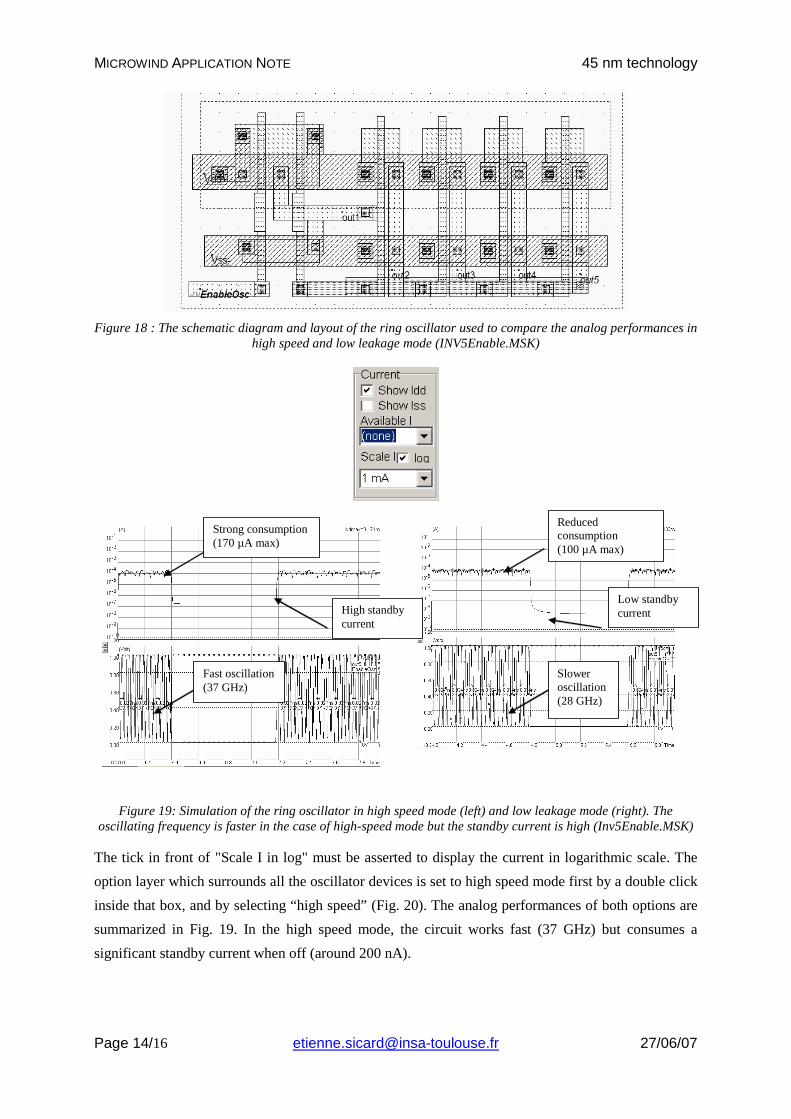
Let us consider the ring oscillator with an enable circuit, where one inverter has been replaced by a
NAND gate to enable or disable oscillation (Inv5Enable.MSK). The schematic diagram of the
oscillator and its layout implementation are shown in Fig. 18. We analyze its switching performances,
as shown in Fig. 19, in the high speed and low leakage modes.
MICROWIND APPLICATION NOTE 45 nm technology
Page 14/16 [email protected] 27/06/07
Figure 18 : The schematic diagram and layout of the ring oscillator used to compare the analog performances in
high speed and low leakage mode (INV5Enable.MSK)
Strong consumption (170 µA max)
High standby current
Fast oscillation (37 GHz)
Slower oscillation (28 GHz)
Low standby current
Reduced consumption (100 µA max)
Figure 19: Simulation of the ring oscillator in high speed mode (left) and low leakage mode (right). The oscillating frequency is faster in the case of high-speed mode but the standby current is high (Inv5Enable.MSK)
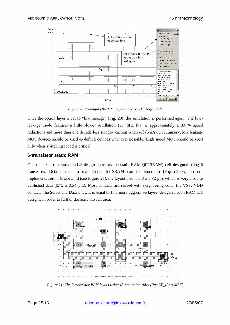
The tick in front of "Scale I in log" must be asserted to display the current in logarithmic scale. The
option layer which surrounds all the oscillator devices is set to high speed mode first by a double click
inside that box, and by selecting “high speed” (Fig. 20). The analog performances of both options are
summarized in Fig. 19. In the high speed mode, the circuit works fast (37 GHz) but consumes a
significant standby current when off (around 200 nA).
MICROWIND APPLICATION NOTE 45 nm technology
Page 15/16 [email protected] 27/06/07
(1) Double click in the option box
(2) Modify the MOS option as « low leakage »
Figure 20: Changing the MOS option into low leakage mode
Once the option layer is set to “low leakage” (Fig. 20), the simulation is performed again. The low-
leakage mode features a little slower oscillation (29 GHz that is approximately a 30 % speed
reduction) and more than one decade less standby current when off (5 nA). In summary, low leakage
MOS devices should be used as default devices whenever possible. High speed MOS should be used
only when switching speed is critical.
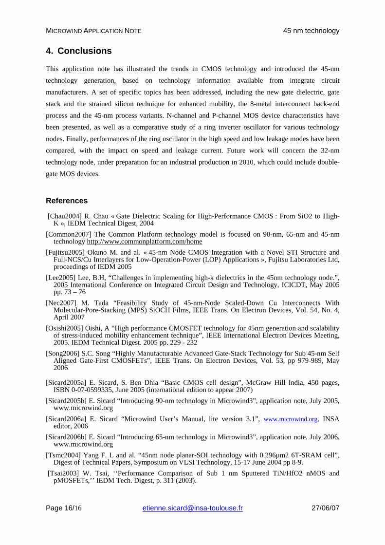
6-transistor static RAM
One of the most representative design concerns the static RAM (6T-SRAM) cell designed using 6
transistors. Details about a real 45-nm 6T-SRAM can be found in [Fujitsu2005]. In our
implementation in Microwind (see Figure 21), the layout size is 0.8 x 0.32 µm, which is very close to
published data (0.72 x 0.34 µm). Most contacts are shared with neighboring cells: the VSS, VDD
contacts, the Select and Data lines. It is usual to find more aggressive layout design rules in RAM cell
designs, in order to further decrease the cell area.
Figure 21: The 6-transistor RAM layout using 45-nm design rules (Ram6T_45nm.MSK)
MICROWIND APPLICATION NOTE 45 nm technology
Page 16/16 [email protected] 27/06/07
4. Conclusions
This application note has illustrated the trends in CMOS technology and introduced the 45-nm
technology generation, based on technology information available from integrate circuit
manufacturers. A set of specific topics has been addressed, including the new gate dielectric, gate
stack and the strained silicon technique for enhanced mobility, the 8-metal interconnect back-end
process and the 45-nm process variants. N-channel and P-channel MOS device characteristics have
been presented, as well as a comparative study of a ring inverter oscillator for various technology
nodes. Finally, performances of the ring oscillator in the high speed and low leakage modes have been
compared, with the impact on speed and leakage current. Future work will concern the 32-nm
technology node, under preparation for an industrial production in 2010, which could include double-
gate MOS devices.
References
[Chau2004] R. Chau « Gate Dielectric Scaling for High-Performance CMOS : From SiO2 to High-K », IEDM Technical Digest, 2004
[Common2007] The Common Platform technology model is focused on 90-nm, 65-nm and 45-nm technology http://www.commonplatform.com/home
[Fujitsu2005] Okuno M. and al. « 45-nm Node CMOS Integration with a Novel STI Structure and Full-NCS/Cu Interlayers for Low-Operation-Power (LOP) Applications », Fujitsu Laboratories Ltd, proceedings of IEDM 2005
[Lee2005] Lee, B.H, “Challenges in implementing high-k dielectrics in the 45nm technology node.”, 2005 International Conference on Integrated Circuit Design and Technology, ICICDT, May 2005 pp. 73 – 76
[Nec2007] M. Tada “Feasibility Study of 45-nm-Node Scaled-Down Cu Interconnects With Molecular-Pore-Stacking (MPS) SiOCH Films, IEEE Trans. On Electron Devices, Vol. 54, No. 4, April 2007
[Osishi2005] Oishi, A “High performance CMOSFET technology for 45nm generation and scalability of stress-induced mobility enhancement technique”, IEEE International Electron Devices Meeting, 2005. IEDM Technical Digest. 2005 pp. 229 - 232
[Song2006] S.C. Song “Highly Manufacturable Advanced Gate-Stack Technology for Sub 45-nm Self Aligned Gate-First CMOSFETs”, IEEE Trans. On Electron Devices, Vol. 53, pp 979-989, May 2006
[Sicard2005a] E. Sicard, S. Ben Dhia “Basic CMOS cell design”, McGraw Hill India, 450 pages, ISBN 0-07-0599335, June 2005 (international edition to appear 2007)
[Sicard2005b] E. Sicard “Introducing 90-nm technology in Microwind3”, application note, July 2005, www.microwind.org
[Sicard2006a] E. Sicard “Microwind User’s Manual, lite version 3.1”, www.microwind.org, INSA editor, 2006
[Sicard2006b] E. Sicard “Introducing 65-nm technology in Microwind3”, application note, July 2006, www.microwind.org
[Tsmc2004] Yang F. L and al. “45nm node planar-SOI technology with 0.296µm2 6T-SRAM cell”, Digest of Technical Papers, Symposium on VLSI Technology, 15-17 June 2004 pp 8-9.
[Tsai2003] W. Tsai, ‘‘Performance Comparison of Sub 1 nm Sputtered TiN/HfO2 nMOS and pMOSFETs,’’ IEDM Tech. Digest, p. 311 (2003).