Embed Size (px)
Citation preview

Silicon Micromachined Sensor for Broadband Vibration Analysis
Adolfo Guti_rrez, Daniel Edmans, Chris Cormeau, Gemot SeidlerInterScience, Inc.Troy, NY 12180
and
Dave Deangelist, Edward MabytttDepartment of Mechanical Engineering
ttDepartment of Electrical, Computer and Systems EngineeringRensselaer Polytechnic Institute
Troy, NY 12180-3590
f
/
SBIR Sponsors: DoD AF, DoD ARMY-ARPA
ABSTRACT
The development of a family of silicon based integrated vibration sensors capable of sensing
mechanical resonances over a broad range of frequencies with minimal signal processing requirements is
presented. Two basic general embodiments of the concept were designed and fabricated. The first
design was structured around an array of cantilever beams and fabricated using the ARPA sponsored
MUMPS process at MCNC. As part of the design process for this first sensor, a comprehensive finite
elements analysis of the resonant modes and stress distribution was performed using PATRAN.
Dependence of strain distribution and resonant frequency response as a function of Young's Modulus in
the Poly-Si structural material was studied. Analytical models were also studied. In-house experimental
characterization using optical interferometry techniques were performed under controlled low pressure
conditions. A second design, intended to operate in non-resonant mode and capable of broadband
frequency response, was proposed and developed around the concept of a cantilever beam integrated
with a feedback control loop to produce a null mode vibration sensor. A proprietary process was used to
integrate a MOS sensing device, with actuators and a cantilever beam, as part of a compatible process.
Both devices, once incorporated as part of mutifunction data acquisition and telemetry systems will
constitute a useful system for NASA launch vibration monitoring operations. Satellites and other space
structures can benefit from the sensor for mechanical condition monitoring functions.
INTRODUCTION
Over the past 10 years the research and development efforts aimed towards producing very small
electromechanical components using microelectronics fabrication techniques have received ever
increasing attention. As a result of these efforts, various competing technologies have emerged as
leading contenders. In Europe, high aspect ratio microstructures fabricated using the LIGA
(Lithographie, Galvanoformung und Abformung) process based on the use of thick photoresist,
synchrotron based x-ray lithography and injection molding has become dominant. Japan, driven by
MITI coordinating efforts, has chosen to miniaturize components through mechanical microfabrication
using high precision machinery. In the United States the most developed technology for the fabrication
of micromachined devices relies on using silicon bulk or surface micromachining.
A typical silicon surface micromachining process begins with a silicon wafer upon which
alternating layers of structural (Poly-Si) and sacrificial material (Si02) are deposited and selectively
etched to produce structures that have relatively small aspect ratios. The thickness of the depositions is
limited to a few microns because of photoresist thickness and etch rate limitations, and because of built-
https://ntrs.nasa.gov/search.jsp?R=19960054122 2018-07-02T22:06:15+00:00Z

in or intrinsic residual stressesthat tend to increase as the thickness of the layers increases. These
process created stresses can only be partially relieved through thermal annealing and the remainingresidual stress can determine severe structural deformations after final chemical release.
Although silicon micromachining of Micro-Electromechanical Systems (MEMS) has rapidly
become a major research area, only a handful of successful commercial devices have been produced.
The consolidation of MEMS devices as a segment of the sensors and microelectronics industry
ultimately will rely on proper product definition, skillful market identification, and competitive cost-
benefit ratios. InterScience, Inc. has decided to focus its research and development efforts in a group of
relatively simple integrated mechanical vibration sensors suitable for real time vibration analysis of
mechanical structures. These types of sensors would have applications in transportation and other
mechanical systems where reliability if of utmost concern. Systems such as launch and orbital vehicles,
permanent space structures, aircrafts and missiles are examples of such systems of direct interest to
NASA, FAA and DoD. Also, high reliability mechanical systems are found throughout the nuclear
cycle. Some potentially mass producible applications, such as engine analysis in the ground and sea
transportation industries, are also readily conceivable. Cost-benefit tradeoffs will ultimately be the
determining factor in the commercial success of these types of sensors.
Earlier work by Benecke and Csepregi I demonstrated the feasibility of building resonant
vibration sensors using a piezoelectric sensor located at the base of the cantilever beams, where the
strain is maximum. Additional work by Motamedi 2 from Rockwell demonstrated cantilever based
accelerometers fabricated in silicon using piezoelectric capacitive sensors and a PMOS amplifier, in a
process fully VLSI compatible. Both sensors exhibited narrow band responses that could potentially be
improved through the use of feedback control schemes. Inspired by these initial investigations, our team
decided to pursue the development of a family of vibration sensors, both resonant and non-resonant,
using silicon surface micromachining 3. The goal of the first effort was to develop a resonant vibration
sensor capable of real time spectral analysis using an array of cantilever beams. The goal of the second
related effort was to produce a wideband vibration sensor incorporating feedback control and integrated
capacitive position sensing.
This paper describes the various aspects that we have encountered in the development of our
vibration sensors. Critical proprietary information has been left out of the discussion. The development
is still an ongoing effort implying that some critical information for performance assessment is missing.
The paper starts with a review of the effort of producing an array of resonant piezoresistive vibration
sensors. It follows with a review of the fabrication process which was used by MCNC in our first
design. Numerical analysis of our sensors, based on finite element methods is then surveyed. It follows
a discussion of the rationale for incorporating feedback forced balance schemes. Finally a discussion of
our in-house mechanical characterization capabilities based on interferometry is presented.
SILICON MICROMACHINED RESONANT VIBRATION SENSOR
A number of functional prototypes were fabricated using the MCNC (formerly Microelectronics
Center of North Carolina) foundry as part of the MUMPS4 (Multi-User MEMS Process, Run # 4). This
multiproject process is supported by ARPA as part of a multi-year infrastructure program for MEMS
development. Figure 1 is a general cross section of the two-layer polysilicon surface micromachining
MUMPs process 4. This process has the general features of a standard surface micromachining process:
(1) polysilicon is used as the structural material, (2) deposited oxide is used as the sacrificial layer, and
(3) silicon nitride is used as electrical isolation between the polysilicon and the substrate.
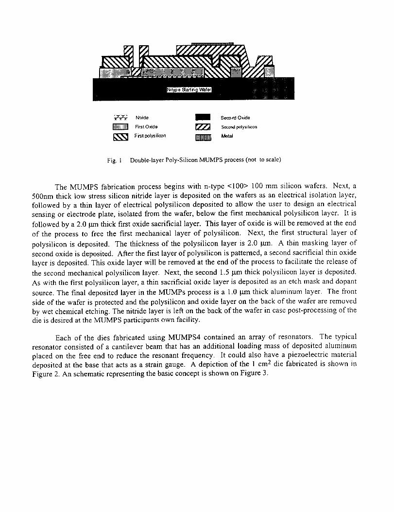
Ntride i Second Oxide
First O_de rZT"J Second polysilicon
Fist polysilicon Metal_llllllllill
Fig. 1 Double-layer Poly-Silicon MUMPS process (not to scale)
The MUMPS fabrication process begins with n-type <100> 100ram silicon wafers. Next, a
500nm thick low stress silicon nitride layer is deposited on the wafers as an electrical isolation layer,
followed by a thin layer of electrical polysilicon deposited to allow the user to design an electrical
sensing or electrode plate, isolated from the wafer, below the first mechanical polysilicon layer. It is
followed by a 2.0 _-n thick first oxide sacrificial layer. This layer of oxide is will be removed at the end
of the process to free the first mechanical layer of polysilicon. Next, the first structural layer of
polysilicon is deposited. The thickness of the polysilicon layer is 2.0 j.trn. A thin masking layer of
second oxide is deposited. After the first layer of polysilicon is patterned, a second sacrificial thin oxide
layer is deposited. This oxide layer will be removed at the end of the process to facilitate the release of
the second mechanical polysilicon layer. Next, the second 1.5 ILtm thick polysilicon layer is deposited.
As with the first polysilicon layer, a thin sacrificial oxide layer is deposited as an etch mask and dopant
source. The final deposited layer in the MUMPs process is a 1.0 pan thick aluminum layer. The front
side of the wafer is protected and the polysilicon and oxide layer on the back of the wafer are removed
by wet chemical etching. The nitride layer is left on the back of the wafer in case post-processing of the
die is desired at the MUMPS participants own facility.
Each of the dies fabricated using MUMPS4 contained an array of resonators. The typical
resonator consisted of a cantilever beam that has an additional loading mass of deposited aluminum
placed on the free end to reduce the resonant frequency. It could also have a piezoelectric material
deposited at the base that acts as a strain gauge. A depiction of the 1 cm 2 die fabricated is shown in
Figure 2. An schematic representing the basic concept is shown on Figure 3.

Figure 3. Cantilevered beam showing placement ofpiezoresistor and loading mass.
Figure 2. A 1 cm2 die containing the first four cantilevertest structures fabricated using MUMPS 4.
IHOglO
Figure 4. Transfer function of a single cantilever beamoscillator.
The resonant frequency of the beam is a function of several parameters including Young's
Modulus of elasticity, the beam length, the thickness of the beam, the density of the polysilicon, and the
density of the surrounding media. A typical transfer function is shown in Figure 4. The selectivity is
represented by the peak at the resonant frequency, fr, and it is characterized by the width at half
maximum power (FWHM), which is strongly dependent on the geometry of the end mass and the
viscosity of the surrounding gas or fluid. For the particular designs implemented, the width of the
resonant peak is about 1 Hz in vacuum and 800 Hz in air at STP. The selectivity and sensitivity are
trade-offs that have to be made to provide the right combination for the particular application. The strain
is related to the driving acceleration and the physical parameters of the beam. The maximum
acceleration that the beam can sustain is given by substituting the maximum yield strength for silicon of
10-3N/m 2 into the strain equation. The resulting value is in the thousands of g's range for our design.
A variable resistance directly proportional to the strain is developed in the piezoelectric crystal. It is also
proportional to the piezoelectric material's coupling coefficient, and the area of the piezoelectric
deposition, and inversely proportional to the combination of the capacitance of the piezoelectric material
and parasitic capacitances.
FINITE ELEMENT ANALYSIS
The critical aspect of the design is the resonant frequency and the mechanical quality factor, Q,
of each cantilever beam. An advantage of a micro-machined vibration sensor, in addition to its small
size and potential for low cost fabrication, is the ability to provide high sensitivity to a discrete set of
vibrational frequencies.
In order to accurately predict the response of the beams to the driving forces, it is necessary to
perform finite element analysis calculations. The use of finite element analysis also provides estimates
for the strain induced at the anchored end of each beam. The strain distribution thus calculated is used

to predicttheoptimumlocationfor thepiezoelectricmaterialin orderto maximizethechargethat willaccumulatein the piezoelectricmaterial,which is directly relatedto the output piezo-voltageto bemeasured.
Initially, thenumericalanalysiswascarriedoutusingthecommercialsoftwarepackagefor finiteelementanalysis,PATRAN. Theanalysisof the shortestcantileverbeamin the array,measuring380pm to the insideedgeof a 300pm squarepaddle. Basedon the finite elementanalysisperformed,theresonantfrequencyof thebeamsvaryfrom 220 Hz to 2,245Hz. It is importantto beawarethattheFEAmodelsrely on a priori knowledge of the Young's Modulus, a parameter that for the case of Poly-Si,
varies significantly for each specific fabrication process. More recently we have centered our numerical
analysis work around the FEA package WECAN.
The fundamental frequency of the beams depicted in this section is much higher than will be
designed and is only being used for illustrative purposes. Figure 5 shows the stress distribution in a
beam that has a paddle on the free end. The paddle reduces the resonant frequency and broadens the
resonant peak. This shows the use of the FEA, to identify areas of high stress during the design process
in order to alleviate any problems by careful early planning.
VI
LI __93'976.
CI _78122"aStressdistlibulionina ca_t_evefbeam and il's$'ubsttale
ca:_:uedby ll'_dell_6on d lhe freeend e_the be_1_
0ulpul_rel:--W_C.AN Step I. lle_ I
Oe_ormed(0.00001 I: Tolal T fan._la_ion
Contour: Plale T,_, Vo,r,Mises Sb'es_:
593743
474994.
35G246.
232"497
119749
0
Figure 5. Stress distribution in a typical beam showing the highest stress concentration at the constrained end.
For a structure which is 1.5 _a thick, 60 l.tm wide and 200 _n long, the fundamental mode,
shown in Figure 7, occurs at 50,859 Hz and the typical deflection is 144 _xrn when it is not constrained.
The stress distribution is represented by the shading. The shape of the deflection is important because
the capacitance will vary as the beam is deflected. At higher modes 3 and 5 the beam twists. The next
four frames in Figure 8 show the shape the beam takes in each of the first four higher order modes,
numbers 2 through 5.

z! ..¥
Output Se'(>_4ode1 50859 Hz
Oelolmed(0 000144]_ Total Tlanda(monConloum:PlateTop Vonk4ise=S_tess
Z
OutputJ_e._NNW_e1 50859. Hz
Deformed(0 000144): T(:XatTklwnsta_ion
Contc,u=:Plale TopVor,b,4ise$Stless
Figure 7. The shape of a simple beam in the fundamental mode.
zL.....A"
Outl_ Sef"A,lode3 348090 Hz
De_oin'md[0.O000338}:TotalT,ew'_l_=)r,
Con4ounPlateTop V_= Stre_
Output Set:)N4ode5 1100100, Hz
Deforrned(0,0000313): Totat Tran.dahonContour: Pla_eTop VonMises Stress:
Figure 8 The first four higher order modes, 2-5, of a typical beam showing the shape and the scaled deflection. The straindistribution is represented by the shading.
The comparison of the normalized deflections shown in the preceding pictures shows that the
maximum displacement associated with the higher order modes is always less than 30% of the
displacement of the beam in its fundamental mode. Figure 9 below shows the relative displacement of
the beam in each of the first five modes relative to the sixth mode. It shows that there is very little
deflection associated with the higher modes, although it cannot be ignored.

Normalized Displacement
i 1
"$ 0.103 I._ tO LO E:, tJ3
tO O O E) 0 O
CO + + + + +
O W W W W W
Frequency
Figure 9 Relative deflection of the beam in each of the first six modes.
The resonant vibration sensor was determined to be adequate for applications in which a priori
knowledge of the mechanical frequencies is available. Although in principle it is possible to cover a
large spectral range through the use of a very large number of cantilever beams, in practice however, this
approach will result in large and highly redundant devices, implying high unit cost. Furthermore,
resonant devices impose severe packaging restrictions since they require vacuum sealed operation to
reduce viscous damping.
A concept that has been used for several decades in the field of seismology is the null mode
forced balance feedback operation of an inertial vibration sensor which improves all the mechanical
performance figures. It enables wider broadband, higher sensitivity and simplified packaging
requirements.
SILICON MICROMACHINED WIDEBAND NON-RESONANT VIBRATION SENSOR
The force-balance vibration sensor derives its name from the forces applied electrostatically
between its suspended mass and frame through the use of a feedback loop. Two forces are involved, one
variable force proportional to the displacement of the mass relative to the frame that tends to balance this
displacement and so behaves as a variable spring, a second force is proportional to the relative velocity
and provides lossless dynamic damping.
I Resonanl Gale Transislol ](Modulator)
Input
Si_._ Can,,I .... Beam !
] Outpu_t Signal-b"- i Feedback Function
[ j
Control Electrodes(Driver)
Figure I0. Force-balance feedback control block diagram.

The fundamental equation describing any inertial vibration sensor isS:
d2x, +R dx + 1 _ d2xi_Xr --_
dt 2 M dt MC dt 2
where M is the suspended mass, xi is the external mechanical excitation,
resistance and C is the compliance of the supporting spring.
Acceleration
x,__@
X r
il"e
H(f) _ AVibration Sensor Transducer & Amplifier
8
Feedback Ne_od_
R is the viscous damping
VC
Figure 11. Force-balance feedback control diagram
The application of negative force-feedback to a seismometer produces a number of advantages
and is in fact essential when a small mass is suspended with a high Q, in order to achieve a satisfactory
transient response. The most useful form of feedback is negative displacement, which tends to keep
the mass fixed in a position with respect to its support, making the suspension appear more stiff and
increasing the natural frequency.
The transfer function of the vibration sensor represented in Fig. 11 is •x, 1
xi s2 + 2_(OoS + tooz
s=jw is the Laplace operator and _ is the damping ratio. The closed-loop transfer function is
v.__oo= A•. 2
Xl S2 + 2E(O0S + 0)0
where vo is the output voltage, A is the gain in the forward path and B is the transfer function of the
feedback path, and becomes I/B when AB is the dominant term. If it is assumed that AB is independent
of frequency, the DC loop gain L is (1/¢0o2)AB and the natural frequency is increased by a factor L 1/2,
the damping being reduced by the same factor. The response is essentially flat (to acceleration) from
DC to the new natural frequency and the transient response can be controlled by a compensation
network in the feedback path.
The fundamental limit of detection of any vibration sensor is determined by the Brownian
motion of the mass. It has been shown that the noise equivalent acceleration (d2xi/dt 2) for a bandwidth f
is given by
4RkTl_f _4kT OJo
(x)l"'-- M 2 M Q
where kT is the equi-partition energy and Q is the quality factor of the suspension. It can be observed
that a small mass may be used provided that the damping is low. A typical micromachined device, such
as the one we have developed has a mass of about 0.3 !ag, Q of about 1000, and a natural frequency of a
lkHz which determines that the noise equivalent acceleration is about 3.5 x l0 -13 m2s -3. In fact this

device is extremely sensitive, thus Brownian noise will not be important and the electronic noise, mainly
thermal, will ultimately determine the sensitivity of the micro seismometer.
Mechanical design requirements are eased and the desired wideband response is simply
determined by the feedback parameters. The signal-to-noise is unaffected by feedback. The response is
controlled by applying forces to the mass; this does not affect the Brownian motion, whereas adding
damping to control the response in an open loop-system increases the dissipation and therefore increases
the Brownian motion. Furthermore, it is easy to verify that a very small mass can be suspended with a
high Q and employed in a feedback system of suitable loop gain, can thus provide a flat response and
adequate detectivity over the whole range of interest in seismology. Additionally advantages, over
conventional open-loop instruments are obtained in linearity, dynamic range and calibration.
In the control loop shown in Figure 10, two electronic transducers are attached to the sensor, one
being the modulator, in our case our proprietary capacitive sensing device, and the other being a driver
or control electrodes to provide mechanical force opposing the displacement. The cross section of a
device currently being fabricated that implements this closed feedback control loop is shown in Figure12. It can be observed in the cross-sectional view that two control electrodes have been inserted. The
sensing element of the loop is a proprietary capacitance measuring device.
!:-. i:!
]Poly 1
l Poly 2
_7"_ Poly 3
D Nitride
_] Phosphosilicate Glass (PSG)
]Silicon Dioxide (Si02)
f-_ Single Crystal Silicon (SCS)
Figure 12 Cross-sectional view of the Silicon Micromachined Wideband Vibration Sensor.
EXPERIMENTAL CHARACTERIZATION USING OPTICAL INTERFEROMETRY
TECHNIQUES
Following fabrication of a vibration sensor die, they must be tested and characterized. This is
accomplished by using an interferometric technique developed in our own laboratories. A diagram of
the optical test set-up used to characterize the frequency response of the resonators is shown in Figure
13. A Fabry-Perot (FP) type interferometer is to be used to measure very small deflections of the
cantilever beam. In general an FP interferometer contains two plates separated by a gap. In the case of
the FP interferometer used here, the first plane is a partial reflector, formed by the end surface of the
fiber. The total reflector is the silicon target. Provided that the resonator is moving, the standoff
distance will change producing a changing interference pattern. The fringe pattern can be resolved using
our system to an accuracy of L/30 or up to +_27 nm for an 820 nm wavelength source.

Coherent light source
E0 >
fiber with surface as
partial reflector-ri id
3
beam as
total reflector movable
stand-off-distance d
Figure 13. Fabry-Perot-Interferometer based on single mode fiber interface.
The fringe visibility is given as
/max - Imina=
/max + lmin
where Ima x and Imi n are the relative maxima and minima of the intensity in the range of d+_Ad. The
deflection of the beam, which is variation of the stand-off distance, will change with the applied voltage.
The resulting optical phase difference varies linearly. The optical phase difference (a(t) corresponds to
_t) =-_d(t)
where d(t) is deflection of the beam and Z is the wavelength of the light source.
The beam is deflected with the application of a modulation current through the electrode. A
variety of deflection waveforms can be used to characterize the material parameters and the response of
the beam. A moving beam will modulate the frequency of the interferometric signal. In addition, a
reference signal is needed to differentiate the motion of the vibrating beam from any residual motion of
the surrounding support structure. The reference signal is achieved by a second interferometer that is
pointed to the die substrate. Figure 14 shows the setup of the measurement system.
Mono Mode Fibers (rigid)
ControlElectrode
Computer
FFT
Figure [4. Setup for measuring the movement of the beams.

As mentioned above, the data resulting from this interferometric system is acquired using
LabView. This software package is used to both control laboratory equipment and to analyze the
resulting measurements through the use of virtual instruments. However, an illustrative example is
included below. First data is collected and processed to show the magnitude and phase of the signal.
This data is consequently processed to determine the spectral content. The information in the frequency
domain will include the fundamental frequency as well as a beat frequency generated from the mixing
that occurs due to the nature of the interferometric system. This beat frequency comes from the
convolution of the two signals, one is the reference and the other is the beam itself. Figure 15 shows the
results of the analysis with the spectral content of the beam response clearly shown.
FFT Interferorneter Siqnals
Front Pane)
Figure 15. Results screen of virtual instrument showing the spectrum producedfrom the Fourier
Transform and the impulse response of the beams.
CONCLUSIONS
The evolutionary development of a micromechanical vibration sensor has been described
Starting from a preliminary concept implemented using the ARPA sponsored MUMPS at MCNC, th_
fabrication and characterization of a number of resonant vibration sensor was carried out. During
characterization of this type of sensor, it was determined that viscous damping imposes severe
limitations on the performance of the simple resonators indicating the need for vacuum sealed
encapsulation of the devices.
Finite element modeling efforts were able to provide qualitative information. The fact that the
Young's Modulus for Poly-Si can assume a wide range of values requiring experimental determination
for each particular process, reduces the quantitative potential of the FEA in earlier design stages.
The use of a closed feedback control loop in a configuration known as force balanced vibration
sensor, has the advantage of enabling broadband operation thus simplifying the number of cantilever
sensors required at expense of higher processing complexities. At present we are still carrying out the
various fabrication steps and currently this second set of devices is awaiting final processing.
Metrological characterizationof the devices has been implemented using a fiber opticinterferometric techniquedevelopedat InterSciencethat has beensuccesfully applied for directlymeasuringdeflectionandfrequencyresponseof cantilevertypevibrationsensors.
1 W. Benecke,L. Csepreguiet al, "A frequencyselective,piezoresistivesilicon vibrationsensor",3rdInternationalConferenceon Solid-StateSensorsandActuators,1985,pp. 105-108.
2 M.E. Motamedi,et al., " Applicationof electrochemicaletch-stopin processingsiliconaccelerometer",Proc.1982ElectrochemicalSocietyMeeting,May 9-14,p 188.
3 DoD sponsoredboth efforts underUSAF contract#F29601-94-C-0095 and under ARPA/BMDOcontract number DASG60-94-C-0081.
4 D. Koester, R. Mahadevan and K. Markus, "MUMPs: Introduction and Design Rules", Rev. 3, MCNC,Oct. 1994
5 M.J. Usher et al., "A miniature wideband horizontal-component feedback seismometer", Journal of
Physics E: Scientific Instruments 1977 Vol. 10