Embed Size (px)
Citation preview

9
Silicon Oxide Films Containing Amorphous or Crystalline Silicon Nanodots
for Device Applications
Diana Nesheva1, Nikola Nedev2, Mario Curiel3, Irina Bineva1, Benjamin Valdez2 and Emil Manolov1
1Institute of Solid State Physics, Bulgarian Academy of Sciences, Sofia 2Institute of Engineering, Autonomous University of Baja California, Mexicali, B. C.
3Centro de Nanociencias y Nanotecnología, Universidad Nacional Autónoma de México Ensenada, B. C.
1Bulgaria 2Mexico
1. Introduction
Тhe impressive recent growth of the portable systems market (mobile PC, MP3 audio player, digital camera, mobile phones, hybrid hard disks, etc.), has increased the interest of the semiconductor industry on non-volatile memory (NVM) technologies. Тhe demand for mobility applications is the main reason for the fast development of NVM technologies and products. Therefore lower power consumption, lower system costs, ever higher capacity and system performance are required. The conventional floating-gate memories satisfy these needs at present but the scaling of these memories is becoming increasingly difficult primarily because reliability problems limiting the bottom (tunnel) oxide to a thickness of around 10 nm.
The application of discrete storage nodes in conventional non-volatile memory has been considered as one of the key items for ensuring a better reliability of the non-volatile memory and to increase scaling. The basic idea is to replace the floating gate (FG) of NVMs by many discrete trapping centers. The most important effect of the localized trapping is the fact that a single leakage path due to a defect (intrinsic or created during the operation by the applied write/erase electric field) in the oxide can only discharge a few storage nodes. In the devices with discrete storage nodes, the storage medium consists either of natural traps, normally in a nitride layer (Eitan et al., 2000; Minami et al., 1994), or of semiconductor nanocrystals (Tiwari et al., 1995).
Two kinds of semiconductor structures containing nanocrystals are studied recently for non-volatile memory purposes. Ones of them are metal-insulator-semiconductor (MIS) structures containing semiconductor nanocrystals in the insulator layer. In such structures nanocrystals serve as charge storage media replacing the floating gate in conventional memory field effect transistors (FETs) (Horváth&Basa, 2009; Lombardo et al., 2004; Steimle et al., 2007; Tiwari et al., 1995). The other ones are the phase-change memory structures (which are not subject of consideration in this chapter), where the channel layer itself is
www.intechopen.com

Quantum Dots – A Variety of New Applications
184
switched between nanocrystalline and amorphous state with high and low conductivity, respectively (Hudgens&Johnson, 2004).
Since MIS structures containing semiconductor nanocrystals are less vulnerable to charge loss through isolated defects in the bottom oxide they provide opportunity for reduction of the size of the memory device and for operation at lower voltages compared to continuous floating gate flash devices. They use processes of direct charge tunnelling to the nanocrystals, Fowler-Nordheim tunnelling or channel hot electron (CHE) injection. The result is capturing of one or a few electrons in a potential well with well defined spatial position (Tsoukalas et al., 2005). The captured electron controls the current through a conducting channel situated close to the position of the captured electron and thus the nanocrystal plays the role of a floating gate. The electron stays in the nanocrystal for a certain time, which determines the duration of the “memory” effect in the device (i.e. the retention time).
At room temperature the memory effect, i.e. the charge capture in nanocrystals, manifests itself as a well defined shift of the capacitance-voltage (C-V) dependence of MIS structure (as a result of its charging or discharging) and as a change of the threshold voltage, called memory window, of the transistors fabricated with the same gate dielectric. The reduced density of states in the NCs restricts the states available for electrons and holes to tunnel to. Besides the Coulomb blockade effect arises from a larger electrostatic energy associated with placing a charged particle onto a rather small capacitance. Due to the both effects less charged carriers are used in the operation of the device that results in low-power operation without sacrificing speed. In addition, because the charge loss through lateral paths is suppressed the constraints on electrical contact isolation can be relaxed which permits thinner oxides and therefore lower voltage/power operation. An important advantage of the NVMs containing NCs is that they have shown a superior endurance at increased temperatures than the standard polysilicon floating gate NVMs and those using charge storage in natural traps. More detailed information on the principles of operation and non-volatile memories containing semiconductor or metal nanoparticles in various matrices can be found in a number of recent reviews [see for example (Horváth&Basa, 2009; Steimle et al., 2007; Tsoukalas et al., 2005).
The attention in this chapter is addressed to properties of memory structures in which the standard floating gate is replaced by crystalline or amorphous silicon nanoparticles (NPs), as storage nodes, separated by silicon oxide. The insulator of such MIS structure normally consists of three layers (Dimitrakis et al., 2005; Tiwari et al., 1996; Tsoi et al., 2005): (i) ultra thin tunnel SiO2 layer grown on the crystalline Si wafer followed by (ii) composite layer of Si nanocrystals (NCs) in a SiO2 matrix (nc-Si- SiO2) and (iii) control SiO2 layer, which insulates the NCs from the control gate. The middle nc-Si-SiO2 layer has been mostly prepared by ion
implantation of Si in thermal SiO2 and subsequent annealing at high temperature ( 900 0С) (Normand et al., 2004 and references therein; Carreras et al., 2005; Ng et al., 2006a), by applying some chemical vapor deposition (CVD) technique for Si nanocrystals fabrication and subsequent CVD deposition of silicon dioxide (Lombardo et al., 2004; Oda et al., 2005; Rao et al., 2004), by deposition of a ultra thin amorphous Si layer and a subsequent oxidation of this layer at a high temperature (Kouvatsos et al., 2003; Tsoi et al., 2005) or by thermal evaporation of SiO powder under selected oxygen pressure (Lu et al., 2005, 2006).
The principal materials science aspects of the fabrication of two dimentional arrays of Si nanocrystals in thin SiO2 layers and at tunable distances from the interface with the Si substrate have been considered in Ref. (Claverie et al., 2006). Below we mention only few
www.intechopen.com

Silicon Oxide Films Containing Amorphous or Crystalline Silicon Nanodots for Device Applications
185
interesting points in this respect. The effect of annealing temperature and gas ambient on the properties of nc-Si-SiO2 has been studied in Ref. (Ioannou-Sougleridis et al., 2003). It has been ascertained that the samples annealed at 900 oC show significant memory effect which is a result of electron or hole capture in defect states with approximately same density for both types of carriers (~ 2x1012 cm−2). The hydrogen annealing has shown that the main part of the defect states in these samples is due to unsaturated bonds at the nc-Si/SiO2 interface. In the samples annealed at 1100 oC, the charge capturing does not depend substantially on the hydrogen annealing, which is explained assuming much lower concentration of defect states (~ 2.5x1011 cm−2). In another study (Yu et al., 2003) dependence of the charge effect on the thickness of the nc-Si-SiO2 layer is reported. Depth profiling of the charging effect of the nc-Si has revealed (Liu et al., 2006) that the charging effect decreases with the increase of nc-Si concentration and vanishes when a densely stacked nanocrystal layer is formed. The phenomenon is attributed to charge diffusion among the nanocrystals.
The impact of programming mechanisms Fowler-Nordheim/Fowler-Nordheim or channel hot electron/Fowler-Nordheim on the Performance and Reliability of NVM devices based on Si anocrystals has been explored at both room temperature and 85 0C in Ref. (Ng et al., 2006b). It has been shown that the channel hot electron programming has a larger memory window, a better endurance, and a longer retention time as compared to Fowler-Nordheim programming. Moreover, the channel hot electron programming yields less stress-induced leakage current than the Fowler-Nordheim programming, suggesting that it produces less damage to the gate oxide and the oxide/Si interface.
It has been demonstrated that the application of low-energy ion beam implantation has resulted in preparation of very promising NVMs with Si nanocrystals (Horváth&Basa, 2009; Tsoukalas et al., 2005) since it allows (Normand et al., 1998) to avoid wide distribution of NCs through the oxide layer and to obtain NCs at a specific location into the host matrix. It has been demonstrated that memory cells fabricated following a procedure including implantation with 1 keV silicon ions to a dose of 2×1016 cm−2 and subsequent annealing at 950 0C for 30 min in N2 + 1.5% O2 (Normand et al., 2003; Tsoukalas et al., 2005) displayed more than 106 write/erase ± 9 V/10 ms cycles without observation of gate degradation. The long time extrapolation of the data retention characteristics at two different temperatures, 25 and 85 0C, after + 9 V/− 9 V 10 ms pulses has shown that those Si NC memory device could achieve 10 years data retention at 85 0C. The memory transistors produced displayed about 2 V memory window for the write/erase pulses of ± 9 V, 10 ms.
Low-energy implantation (at 2 keV) has also been applied (Ng et al., 2006a) for preparation of MIS structures in which the tunneling oxide thickness was 3 nm or 7 nm for realization of direct or Fowler-Nordheim tunneling during the charging process. For direct tunneling a memory window width of about 1 V was obtained using charging pulses of ± 12 V, 1 μs. For Fowler-Nordheim tunneling the memory window width was about 0.5 V using charging pulses of ± 12 V, 1 ms. Thus, it has been shown that devices with a thicker tunnel layer required longer charging pulses, and they degraded faster, as well, but the extrapolated for 10 years memory window width at 85 0C was about 0.3 V for both type of structures.
Successful preparation of Si nanocrystals for memory applications has been also realized by chemical vapour deposition. Devices for non-volatile purposes were produced using 3.8-5.0 nm thick tunnel oxide (Rao et al., 2004) and a threshold voltage shift of ~ 1.5 V has
www.intechopen.com

Quantum Dots – A Variety of New Applications
186
been obtained by voltage pulses of 14 V, 100 μs or 12 V, 1 ms. Retention characteristics have also been very good, but the memory window shifted slightly with increasing number of write/erase cycles.
Recently tunnel barrier engineering has been suggested (Jung&Cho, 2008) as a promising way for tunnel oxide scaling. It uses multiple dielectric stacks to enhance field-sensitivity and thus to allow for shorter writing/erasing times and/or lower operating voltages than single SiO2 tunnel oxide without altering the ten-year data retention constraint. Experiments on memory structures containing one-three Si NC layers prepared by evaporation of SiO powder and layer by layer growth (Lu et al., 2005, 2006) have shown that in structures with two or three NC layers two or three different saturation voltages were obtained with increasing bias related to charge injection to and capture at the first, second, or third NC layer (Lu et al., 2005). Charge captured in the first layer yielded a memory window width of about 2.5 V, charge captured in the second NC layer yielded an additional flat-band voltage shift of about 2.5 V, while charge captured in the third layer yielded an additional shift of about 1.5 V. It has been observed that the multilayer storage in memory structures prepared by different deposition methods yielded very good retention, as well (Han et al., 2007; Lu et al., 2005; Nassiopoulou et al., 2009).
For decades the radiation effects have been a serious problem for electronics used in defense and space systems and therefore the study of the radiation effects on metal-oxide-semiconductor (MOS) based devices, including MOS capacitors, has been an active research area over the past decades. An advantage of the nanocrystalline NVMs is their higher tolerance to radiation ionization which can result in memory applications in avionics, nuclear power stations, nuclear waste disposal sites, military, medicine etc. (Gerardi et al., 2011). Besides, MOS structures and transistors with nanocrystals are developed for dosimeter purposes.
Generally MOS structures pose high spatial resolution and their production is compatible with the technology used in the microelectronic industry. Two types MOS transistors are used for detecting of ionizing radiation: radiation-sensing field effect transistor (RADFET) (Buehler et al., 1993; Holmes-Siedle&Adams, 1986; Hughes et al., 1988; Price et al., 2004; Ramani et al., 1997; Stanic et al., 2005) and floating gate transistors (Edgecock et al., 2009; Kassabov et al., 1991; McNulty et al., 2006; Scheick et al., 1998, 1999; Tarr et al., 1998, 2004). Normally the RADFET is a p-channel MOS transistor whose SiO2 gate is grown at specific conditions and its thickness is around 1 μm (Sarrabayrouse, 1991 ). A part of the charge carriers generated by the ionizing radiation is trapped in the oxide and the integrated irradiation dose is detected as a change in the transistor threshold voltage. To ensure good sensitivity of these dosimeters an electric field is normally applied on the control gated during irradiation. The radiation induces changes are irreversible and therefore RADFET dosimeters are for a single use only. At the floating gate dosimeter before irradiation the floating gate is charged by electron injection from the control gate (Kassabov et al., 1991; Tarr et al., 1998) or substrate (Martin et al., 2001) and this creates an electrical field in the oxide layer. Therefore no application of external electric field is necessary during irradiation which makes their application more convenient. In addition, the radiation induces changes which are reversible and multiple usage of those dosimeters is possible. Recently, experiments have been performed (Aktag et al., 2010) on introduction of Ge nanocrystals in the oxide layer of floating gate dosimeters. It has been
www.intechopen.com

Silicon Oxide Films Containing Amorphous or Crystalline Silicon Nanodots for Device Applications
187
observed that the presence of nanocrystals improves the radiation resistance of detectors but decreases their sensitivity.
In this chapter a review is made of the most important results obtained during the last five years by the authors and their collaborators in the field of development of metal-insulator-silicon structures with dielectric film containing amorphous or crystalline silicon nanoparticles, which are suitable for non-volatile memory and radiation applications. In the
introductory part a brief review of the results of other research groups on MIS structures containing Si nanoparticles for non-volatile memory and detector applications has been made. The next second part gives information about the preparation of SiOx films of different compositions and the annealing conditions used for the growth of amorphous (na-Si) and crystalline (nc-Si) silicon nanoparticles. Infrared absorption and Rutherford backscattering data give information on the oxygen content, while X-ray Diffraction and Reflectivity, X-ray Photoelectron Spectroscopy, Transmission Electron Microscopy, Atomic Force Microscopy, Infra Red Transmission and, Raman Scattering spectroscopy and Spectroscopic Ellipsometry data give information about the effect of furnace annealing on the properties of the SiOx films. In the third part newly developed techniques for preparation of MIS structures containing amorphous and crystalline Si nanoparticles suitable for non-volatile memory application are described. The fabricated MIS structures are characterized by high frequency (100 kHz and 1 MHz) capacitance/conductance-voltage (C/G-V) measurements at applied dc voltage varying within a voltage range 15 V. The
last fourth part presents recent data on preparation of MIS structures containing Si nanocrystals and their response to γ-radiation.
2. Preparation of SiOx films and growth of amorphous and crystalline Si nanoparticles
It is well known that the film preparation and processing are very important for the
performance of the MIS structures and devices with nanocrystals. They determine the film
composition, which in the case of Si NP growth by SiOx film annealing is of critical importance
for the nanocrystal size, the filling of the oxides matrix with NCs (NC filling factor), the quality
of the interface with the Si substrate, etc. Therefore this part of the chapter describes results
from a thorough characterization of the SiOx films. This information is important since these
films are an essential part of the two(multi)layer insulator in the MIS structures described in
Parts 3 and 4; they are the layers that contain Si NPs.
2.1 Preparation of SiOx films
SiOx layers with an initial composition of x = 1.1 and 1.3 and thickness of ~ 15 nm were prepared by thermal evaporation of SiO at a vacuum of 1 × 10⁻³ Pa on n- or p-type (100) c-Si
(4 - 6 and 1 Ωcm, respectively) substrates maintained at room temperature. The SiO evaporation was carried out from a tantalum crucible provided with a molybdenum cylindrical screen and thus evaporation in a quasi-closed volume takes place (Nesheva et al., 2003). The film thickness and deposition rate were monitored by a quartz microbalance system. Before the films deposition the silicon wafers were cleaned chemically using a standard procedure for the microelectronics industry. For Raman scattering, infra red and optical transmission measurements SiOx films with same compositions but with thickness of
www.intechopen.com

Quantum Dots – A Variety of New Applications
188
0.2 and 1 μm were deposited on c-Si and quartz substrates. The film composition has been determined by means of Rutherford Back Scattering (Nesheva et al., 2003).
All as-deposited layers were annealed at 250 0C for 30 min in an Ar atmosphere to keep them stable at room conditions. In order to grow Si nanoparticles an additional annealing at 700 0C in Ar or 1000 0C in N2 atmosphere for 60 min was carried out.
2.2 Si nanoparticle growth, oxygen matrix densification, interface quality
The films annealed at high temperatures as well as control ones (annealed at 250 0C) were characterized by Transmission Electron Microscopy (TEM), Raman Spectroscopy, X-ray Diffraction (XRD) and Reflectivity (XRR), X-ray Photoelectron Spectroscopy (XPS) and Atomic Force Microscopy (AFM). Lattice-resolution TEM was carried out at 200 kV with a JEOL 2100 with a point-to-point resolution of 0.22 nm in the TEM mode. XRD/XRR measurements were performed using Philips X´pert Diffractometer (Cu Kα source), XPS analysis by Kratos Axis Ultra spectrometer (Al Kα (1486.6 eV) X-ray source), Raman spectra using Witec α-SNOM and AFM micrographs were taken by Asylum Research Microscope in tapping mode. Cross-sectional TEM (XTEM) samples were also prepared by gluing film-to-film two Si wafers and then cutting vertical sections which were first mechanically thinned to a thickness of 25 μm. Final thinning to electron transparency was accomplished by ion milling at very low angles (15° - 10°) from both cross-sectional sides. Optical and infra red transmission measurements were also carried out by means of Cary 5E, Perkin-Elmer Spectrum One FTIR and Bruker Vertex 70 spectrophotometers, respectively.
Raman scattering spectra of SiOx films with thickness of 1 μm deposited on quartz substrates and annealed at 700 0C and 1000 0C for 60 min are shown in Fig.1. A broad band centered at ~ 470 cm-1 is observed in the spectrum of the film annealed at 700 0C. It is typical for amorphous silicon (Iqbal&Veprek, 1982; Nesheva et al., 2002) and its observation can be
300 400 500 600
Si-nanocrystals
amorphous
nanoparticles
Tann
1000 °C
700 °C
Inte
nsi
ty (
arb. unit
s)
Raman shift (cm-1)
Fig. 1. Raman scattering spectra of SiOx films (1 μm thick) deposited on quartz substrates and annealed at 700 0C or 1000 0C.
www.intechopen.com

Silicon Oxide Films Containing Amorphous or Crystalline Silicon Nanodots for Device Applications
189
250 500 750 1000 1250 1500
0
20
40
60
80
100
Tann
substrate
700oC
250oC
Tra
nsm
issi
on (
%)
Wavelength (nm)
SiO1.15
Fig. 2. Optical transmission spectra of two SiO1.15 layers annealed at 250 and 700 0C. A red shift is observed upon annealing at 700 0C.
related to existence of pure amorphous silicon phase in these films. Such band is not seen in the spectrum of the film on quartz substrate annealed at 1000 0C, which confirms that the band at 470 cm-1 is related to a-Si phase rather than to light scattering from the SiOx matrix or SiO2 substrate. An asymmetric band peaked at ~ 518 cm-1 is observed in the spectrum of the film annealed at 1000 0C, which cannot originate from the quartz substrate and its appearance is an evidence for the existence of Si nanocrystals (Iqbal&Veprek, 1982).
The existence of pure silicon phase in the films annealed at 700 0C has also been confirmed by optical transmission measurements carried out on SiOx layers on quartz substrates. Figure 2 shows optical transmission spectra of a sample with x = 1.15 measured before and after annealing at 700 0C. It is seen that the annealing causes a “red” shift of the spectrum. Since the increase of the oxygen content in the matrix should result in a “blue” shift, the observed “red” shift is an indication that absorption in a pure silicon phase takes place. A value of 2.64 eV has been obtained for the optical band gap of the amorphous Si particles grown upon annealing of samples with x = 1.15 at 700 0C and a value of 2.1 nm has been estimated for the average diameter of the largest amorphous Si NPs in our films (Nesheva et al., 2008).
Figures 3 (a) and (b) show XTEM micrographs of a control (250 0C) and an annealed at 1000 0C sample with x = 1.3 and thickness of 15 nm. Figure 3 (a) exhibits an amorphous structure and a nearly atomically flat interface, while Figure 3 (b) exhibits randomly oriented nanocrystals with a diameter of ~ 4-5 nm and an increase of the roughness of the c-Si wafer/dielectric interface. The NCs are positioned closer to the c-Si wafer than to the top SiOx surface and are separated from the c-Si/SiOx interface by an amorphous region with thickness ≥ 3 nm. The thicknesses of the SiOx layers determined are of 16.2 nm and 13.8 nm for the control and annealed sample, respectively. While the thickness of the control film is close to the one set during the deposition, film densification of about 15% has been concluded in result of the annealing at 1000 0C for 60 min.
The XRD results of control and 1000 0C annealed samples obtained in the 2Θ/Ω scans show (Fig. 4) only two peaks at 33o and 68o corresponding to diffraction from the crystalline Si
www.intechopen.com

Quantum Dots – A Variety of New Applications
190
Fig. 3. Cross-sectional (XTEM) micrographs of a control sample (a) and an annealed at 1000 0C sample with nanocrystals in a dielectric matrix and rougher interface (b).
(100) substrate. No contribution due to the nanocrystals is observed because of the random NCs orientation, as revealed by TEM. The XRR spectra of a control and annealed at 700 and 1000 0C samples are shown in Fig. 5. The well defined interference fringes in the spectrum of the control sample (curve 1) imply an excellent interface between the dielectric and the c-Si wafer. With the increase of the annealing temperature from 700 0C to 1000 0C the amplitude of the interference fringes decreases (curves 2 and 3) indicating an increase of the interface roughness. The obtained results are in good agreement with the XTEM ones. The XRR technique was also applied to determine the thicknesses of the SiOx layers. Values of 16.8 nm for the control and 16.9 and 14.8 nm for the annealed at 700 0C and 1000 0C layers, respectively, have been obtained. The errors in the thicknesses of the control and 1000 0C annealed samples are 3.7 and 7.2 %, respectively. Again, the sample annealed at 1000 0C show a small decrease of the initial thickness while the thickness of the film annealed at 700 0C is practically constant. This observation can be understood if assuming that at 700 0C the disorder of the substoichiometric SiOx matrix is still rather high.
10 20 30 40 50 60 70 80
2
1
Silicon Substrate
Inte
nsity (
arb
. units)
2/ (o)
1 control
2 annealed 1000oC
Fig. 4. 2Θ/Ω scans of a control (1) and annealed at 1000 0C for 60 min (2) samples.
www.intechopen.com

Silicon Oxide Films Containing Amorphous or Crystalline Silicon Nanodots for Device Applications
191
0.0 0.5 1.0 1.5 2.0 2.5 3.0 3.5
3
2
1
Inte
nsi
ty (
arb. unit
s)
2 Theta (o)
1 250 oC
2 700 oC
3 1000 oC
Fig. 5. XRR spectra of a control (1) and annealed at 700 (2) and 1000 0C (3) samples.
XPS was used to obtain further information about the structure and chemical composition of
the 15 nm films. In Figs 6 and 7 spectra of the Si 2p core level of control and annealed layers
with expected x = 1.3 at incidence angles of 30o and 90o, respectively, are presented. The
Gaussian fitting curves are also shown. The main peak in the spectrum of the control sample at
both angles (Figs. 6 (a) and 7 (a)) is positioned at 102.4 eV and corresponds to a SiOx film with
x = 1.35 (Alfonsetti et al., 1993), a value that is close to the composition set by the deposition
conditions. After deconvolution three Gaussians peaked at 103.6, 102.4 and 100.1 eV were
resolved. The peaks at 103.6 and 102.4 eV are attributed to Si-O bonds in pure SiO2 and in
Si2O3 compounds, respectively, while the shoulder at lower binding energy could be
superposition of signals resulting from Si-O bonds in Si2O suboxide and Si-Si bonds in silicon,
having binding energies close to each other, 100.7 eV and 99.8 eV, respectively (Alfonsetti et
al., 1993). In all spectra of the annealed films (Figs. 6 (b), (c), 7 (b), (c)) a well defined peak
positioned at 103.8 eV corresponding to stoichiometric SiO2 is present. This finding seems to be
in disagreement with our previous results about the matrix composition after 700 0C annealing
obtained by IR spectroscopy (Donchev et al., Nesheva et al., 2003, 2008) but the IR
measurements were carried out on thicker films (~ 0.2 μm) and give information about the
volume properties of the films. The XPS signal originates from a region with thickness 10 nm
and one can conclude that most likely the Si nanoscrystals close to the top surface get
transformed into SiO2 to a thickness of ~ 5–6 nm, due to native oxide formation after exposure
to air, as confirmed by XTEM (Fig. 3 (b)). However, there is a substantial difference in the
amplitude of the peak corresponding to pure Si phase (the doublet Si 2p 3/2, Si 2p 1/2 with
binding energies of 99.4 and 99.9 eV) in the spectra of the layer annealed at 1000 0C when
measured at 30o and 90o (Figs. 6 (c), 7 (c)). At angle of incidence of 30o the chemical
composition of the first ~ 3 nm below the film surface is determined, while in the case of
normal incidence the obtained information is for thicker region (~ 10 nm). The observed
difference in the Si peak amplitude can be understood keeping in mind that the nanocrystals
have a diameter of ~ 4-5 nm, they are positioned closer to the c-Si/dielectric interface and the
top 6 - 7 nm of the SiOx film are depleted of NCs (Fig. 3 (b)).
www.intechopen.com

Quantum Dots – A Variety of New Applications
192
108 106 104 102 100 98 96 94
SiO1.35 (a)
Si 2p - 30o
control
Inte
nsity (
arb
. u
nits)
Binding Energy (eV)
108 106 104 102 100 98 96 94
SiO2 (b)
Si 2p - 30o
annealed 700oC
Inte
nsity (
arb
. u
nits)
Binding Energy (eV)
108 106 104 102 100 98 96 94
Si
SiO2
Si 2p - 30o
annealed 1000oC
(c)
Inte
nsity (
arb
. un
its)
Binding Energy (eV)
Fig. 6. Si 2p core level spectra of a control (a) and annealed at 700 0C (b) and 1000 0C (c) layers measured at 30o angle of incidence.
In the case of a-Si nanoparticles formed by annealing at 700 0C the same trend in the
spectra measured at 30o and 90o is observed. Because of the smaller diameter of the a-Si
NPs (~ 2 nm) and probably the same or similar to the nanocrystal spatial distribution the
contribution of the Si phase in the XPS spectra is zero (Fig. 5 (b)) or very small at 90o angle
of incidence (Fig. 6 (b)).
The AFM images in Fig. 8 (a)-(c) show the surface morphology of 15 nm SiOx (x = 1.3) films
annealed at 250 0C, 700 0C and 1000 0C, respectively. The scan area was set to 200 × 200 nm
and the root mean square roughness (RMS) obtained has a value of 0.164 nm for the control
sample (a), 0.258 nm for the 700 0C (b) and 0.129 nm for the 1000 0C (c) annealed samples,
respectively. The AFM measurements revealed that the 700 0C annealing leads to an increase
of the surface roughness which could be due to incomplete phase separation, while the
increase of the annealing temperature to 1000 0C causes a decrease of the surface roughness
and obtaining of smoother films. These results are consistent with the XRR data for the
thickness variation after annealing at 700 0C and 1000 0C.
www.intechopen.com

Silicon Oxide Films Containing Amorphous or Crystalline Silicon Nanodots for Device Applications
193
108 106 104 102 100 98 96 94
SiO1.35 (a)
Si 2p - 90o
control
Inte
nsity (
arb
. u
nits)
Binding Energy (eV)
108 106 104 102 100 98 96 94
Si
SiO2
(b)
Si 2p - 90o
annealed 700oC
Inte
nsi
ty (
arb
. u
nit
s)
Binding Energy (eV)
108 106 104 102 100 98 96 940
10
20
30
40
50 SiO2
Si
(c)
Si 2p - 90o
annealed 1000o C
Inte
nsity (
arb
. un
its)
Binding Energy (eV)
Fig. 7. Si 2p core level spectra of a control (a) and annealed at 700 0C (b) and 1000 0C (c) layers measured at 90o angle of incidence.
The np-Si-SiOx layers are composite materials in which the increase of the volume fraction f of the filler (amorphous or crystalline Si NPs) decreases the distance between the nanoparticles and at a certain concentration contact between some adjacent particles may occur and two- or three-dimensional networks of semiconductor nanoparticles may be formed. As mentioned above, network formation is undesired in the case of NVM devices with NPs and therefore the knowledge of f is important.
Assuming that there is no loss of oxygen atoms upon film annealing, the following relation between f and the atomic densities of the initial layer ρSiOx and pure silicon phase ρSi has been found (Nesheva et al., 2008):
f = (ρSiOx ⁄ ρSi) (x + 1) −1[1 − (x/y)] (1)
where x is the initial oxygen content and y is the oxygen content in the matrix of the annealed layers. Approximate values of f have been obtained using this relation in which the x and y values were determined from the IR transmission data (Donchev et al., in press). It
www.intechopen.com

Quantum Dots – A Variety of New Applications
194
has been obtained that the filling factor changes with the initial oxygen content and for films annealed at 700 0C and 1000 0C it varies between 0.05 and 0.2 and 0.07 and 0.28, respectively, when x decreases from 1.7 down to 1.15. The investigation of the carrier transport
mechanism in 1 m thick films have not shown network formation in high temperature annealed films. In the films annealed at 700 0C containing a-Si NPs, Poole–Frenkel transport mechanism has been observed while tunneling has been dominating in the films annealed at 1000 0C (Nesheva et al., 2008).
(a)
(b)
(c)
Fig. 8. AFM images of a control (a) and annealed at 700 0C (b) and 1000 0C (c) SiOx films.
www.intechopen.com
Silicon Oxide Films Containing Amorphous or Crystalline Silicon Nanodots for Device Applications
195
3. MOS structures containing amorphous or crystalline Si nanoparticles for non-volatile memory applications
3.1 Experimental details
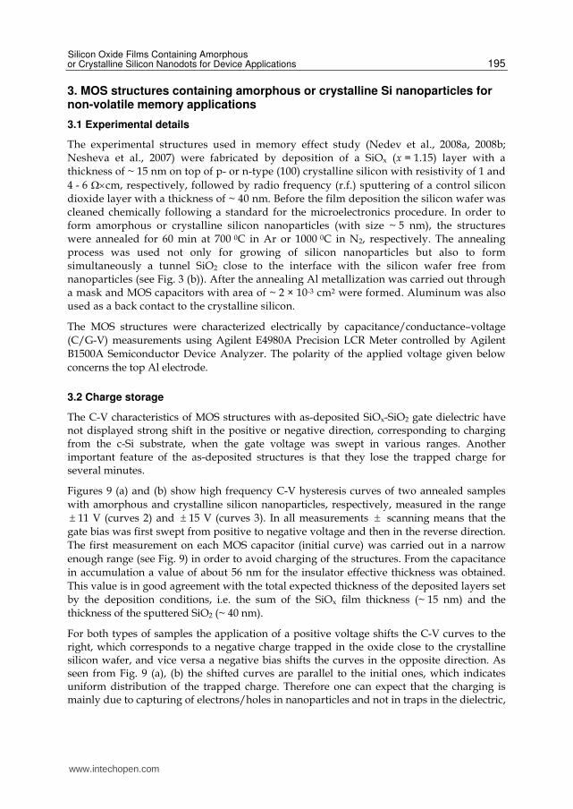
The experimental structures used in memory effect study (Nedev et al., 2008a, 2008b; Nesheva et al., 2007) were fabricated by deposition of a SiOx (x = 1.15) layer with a thickness of ~ 15 nm on top of p- or n-type (100) crystalline silicon with resistivity of 1 and
4 - 6 cm, respectively, followed by radio frequency (r.f.) sputtering of a control silicon dioxide layer with a thickness of ~ 40 nm. Before the film deposition the silicon wafer was cleaned chemically following a standard for the microelectronics procedure. In order to form amorphous or crystalline silicon nanoparticles (with size ~ 5 nm), the structures were annealed for 60 min at 700 0C in Ar or 1000 0C in N2, respectively. The annealing process was used not only for growing of silicon nanoparticles but also to form simultaneously a tunnel SiO2 close to the interface with the silicon wafer free from nanoparticles (see Fig. 3 (b)). After the annealing Al metallization was carried out through a mask and MOS capacitors with area of ~ 2 × 10⁻³ cm2 were formed. Aluminum was also used as a back contact to the crystalline silicon.
The MOS structures were characterized electrically by capacitance/conductance–voltage
(C/G-V) measurements using Agilent E4980A Precision LCR Meter controlled by Agilent
B1500A Semiconductor Device Analyzer. The polarity of the applied voltage given below
concerns the top Al electrode.
3.2 Charge storage
The C-V characteristics of MOS structures with as-deposited SiOx-SiO2 gate dielectric have not displayed strong shift in the positive or negative direction, corresponding to charging from the c-Si substrate, when the gate voltage was swept in various ranges. Another important feature of the as-deposited structures is that they lose the trapped charge for several minutes.
Figures 9 (a) and (b) show high frequency C-V hysteresis curves of two annealed samples
with amorphous and crystalline silicon nanoparticles, respectively, measured in the range 11 V (curves 2) and 15 V (curves 3). In all measurements scanning means that the
gate bias was first swept from positive to negative voltage and then in the reverse direction.
The first measurement on each MOS capacitor (initial curve) was carried out in a narrow
enough range (see Fig. 9) in order to avoid charging of the structures. From the capacitance
in accumulation a value of about 56 nm for the insulator effective thickness was obtained.
This value is in good agreement with the total expected thickness of the deposited layers set
by the deposition conditions, i.e. the sum of the SiOx film thickness (~ 15 nm) and the
thickness of the sputtered SiO2 (~ 40 nm).
For both types of samples the application of a positive voltage shifts the C-V curves to the right, which corresponds to a negative charge trapped in the oxide close to the crystalline silicon wafer, and vice versa a negative bias shifts the curves in the opposite direction. As seen from Fig. 9 (a), (b) the shifted curves are parallel to the initial ones, which indicates uniform distribution of the trapped charge. Therefore one can expect that the charging is mainly due to capturing of electrons/holes in nanoparticles and not in traps in the dielectric,
www.intechopen.com

Quantum Dots – A Variety of New Applications
196
which could have varying spatial and energetic distributions. The value of the clockwise hysteresis is about 4.3 and 9 V (a) and 5.5 and 9.8 V (b) for 11 V and 15 V scanning ranges. The maximum average electric field across the gate dielectric, which corresponds to these scanning ranges, is about 2.0 MV/cm and 2.7 MV/cm, respectively. It is interesting that the C-V characteristics of the a-Si NP structure are much steeper, which indicates lower defect density at the c-Si wafer/silicon oxide interface.
-9 -6 -3 0 3 62.0x10
-11
4.0x10⁻¹¹
6.0x10⁻¹¹
8.0x10⁻¹¹
1.0x10⁻¹⁰
1.2x10⁻¹⁰
Ca
pa
cita
nce
(F
)
Gate bias (V)
1 22 33
(a)
-9 -6 -3 0 3 62.0x10
-11
4.0x10⁻¹¹
6.0x10⁻¹¹
8.0x10⁻¹¹
1.0x10⁻¹⁰
1.2x10⁻¹⁰
Capacitance (
F)
Gate bias (V)
1 22 33
(b)
Fig. 9. C-V dependencies measured in the ranges 11 V (curves 2) and 15 V (curves 3) at 1 MHz of samples with (a) amorphous (b) crystalline silicon nanoparticles. The initial curve 1 was measured in the range +3 V, -7 V for both (a) and (b) samples.
Figures 10 (a) and (b) show the equivalent parallel conductance G vs. gate bias for the two
types of samples. The measurements of G and C were carried out simultaneously in the
same voltage scan. The observed shape of the equivalent parallel conductance, with a peak
in weak inversion, corresponds to energy loss due to carrier generation and recombination
through interface states (Nicollian&Brews, 2002). It is seen that the curves of structures with
a-Si NPs are narrower than those of structures with Si NCs. Also the peak of the parallel
-9 -6 -3 0 3 6
0.0
2.0x10⁻⁵
4.0x10⁻⁵
6.0x10⁻⁵
8.0x10⁻⁵
1.0x10⁻⁴
(a)
Pa
ralle
l co
nd
ucta
nce
(S
)
Gate bias (V)
1 2 323
-9 -6 -3 0 3 6
0.0
4.0x10⁻⁵
8.0x10⁻⁵
1.2x10⁻⁴
1.6x10⁻⁴
(b)
Pa
ralle
l co
nd
ucta
nce
(S
)
Gate bias (V)
1 2
2
33
Fig. 10. Equivalent parallel conductance measured at 1 MHz of samples with (a) amorphous and (b) crystalline silicon nanoparticles. The scanning ranges are the same as for the C-V measurements in Fig. 9.
www.intechopen.com

Silicon Oxide Films Containing Amorphous or Crystalline Silicon Nanodots for Device Applications
197
conductance has smaller value (with about 40 %) for the a-Si NP sample. These results confirm the above conclusion that the structures with a-Si NPs have a better SiO2/c-Si interface than those with Si NCs and are in agreement with the XTEM data (Curiel et al., 2010a, 2010b) where epitaxial overgrowth and increased interface roughness have been found after annealing at 1000 0C (Fig. 3 (b)).
101
102
103
104
105
-2
0
2
4
2
1
1
2 a-Si NP
Si NC
Fla
tband v
oltage s
hift, V
FB (
V)
Time (s)
Fig. 11. Retention characteristics of structures with a-Si NPs (curves 1) and nanocrystals (curves 2) after charging structures negatively with voltage ramp sweep up to +12 V or positively with ramp sweep to -12 V.
The retention characteristics of structures with a-Si NPs and Si NCs were obtained by measuring the time-dependent variation of the flatband voltage (Fig. 11), which is proportional to the area density of the trapped charge (Sze, 1981). In both types of structures the charge loss follows approximately a logarithmic law. An essential advantage of the a-Si nanoparticle structures compared to the NC ones is the much slower discharging process observed, especially of trapped electrons. For example, 48 hours after charging with +12 V the MOS structures containing a-Si NPs still have 75% of the initial charge, while the structures with nanocrystals retain about 43%.
4. Radiation dosimeter based on metal-oxide-semiconductor structures with silicon nanocrystals
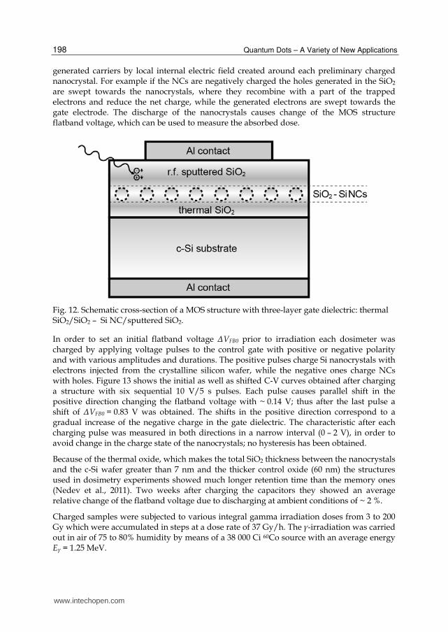
Figure 12 shows schematically a cross-section of the MOS structures used in dosimetry measurements. An essential difference between the dosimetry structures and the ones used in the memory studies is that an additional SiO2 layer, 3.9 nm thick, was grown thermally before the deposition of the SiOx film. The oxidation process was carried out in dry O2 atmosphere at 850 0C. Except for the thermal oxidation and the greater thickness of the control oxide, which for dosimeters was 60 nm, the fabrication process was identical with the one used for fabrication of the memory study samples.
The principle of operation of the proposed dosimeter is based on generation of electron-hole pairs in the SiO2 when the structure is exposed to ionizing radiation and separation of the
www.intechopen.com
Quantum Dots – A Variety of New Applications
198
generated carriers by local internal electric field created around each preliminary charged nanocrystal. For example if the NCs are negatively charged the holes generated in the SiO2 are swept towards the nanocrystals, where they recombine with a part of the trapped electrons and reduce the net charge, while the generated electrons are swept towards the gate electrode. The discharge of the nanocrystals causes change of the MOS structure flatband voltage, which can be used to measure the absorbed dose.
Fig. 12. Schematic cross-section of a MOS structure with three-layer gate dielectric: thermal SiO2/SiO2 – Si NC/sputtered SiO2.
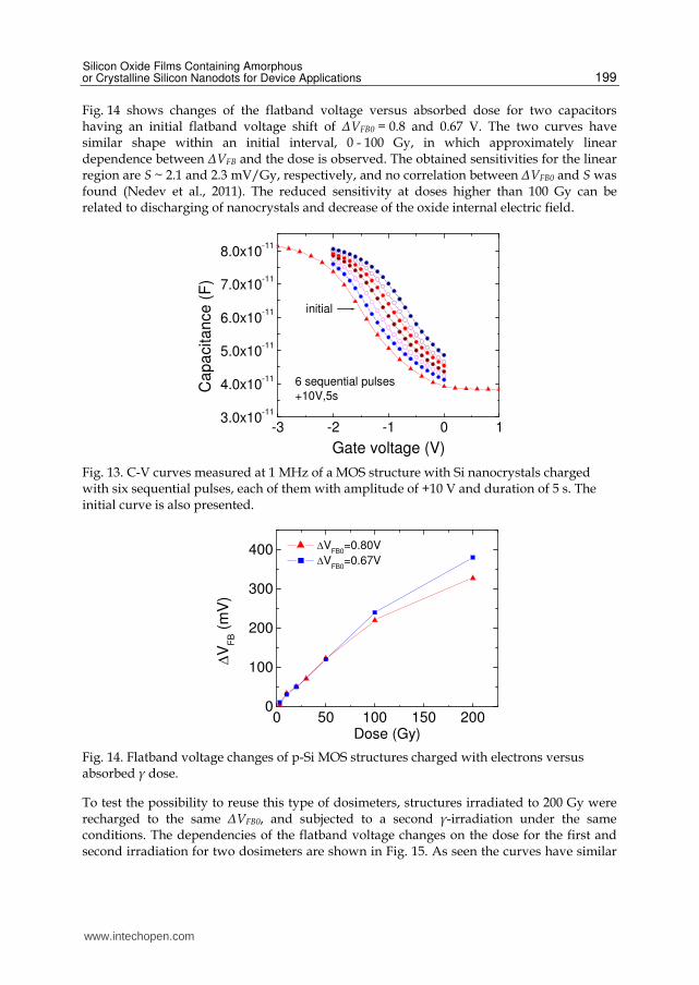
In order to set an initial flatband voltage ΔVFB0 prior to irradiation each dosimeter was charged by applying voltage pulses to the control gate with positive or negative polarity and with various amplitudes and durations. The positive pulses charge Si nanocrystals with electrons injected from the crystalline silicon wafer, while the negative ones charge NCs with holes. Figure 13 shows the initial as well as shifted C-V curves obtained after charging a structure with six sequential 10 V/5 s pulses. Each pulse causes parallel shift in the positive direction changing the flatband voltage with ~ 0.14 V; thus after the last pulse a shift of ΔVFB0 = 0.83 V was obtained. The shifts in the positive direction correspond to a gradual increase of the negative charge in the gate dielectric. The characteristic after each charging pulse was measured in both directions in a narrow interval (0 – 2 V), in order to avoid change in the charge state of the nanocrystals; no hysteresis has been obtained.
Because of the thermal oxide, which makes the total SiO2 thickness between the nanocrystals and the c-Si wafer greater than 7 nm and the thicker control oxide (60 nm) the structures used in dosimetry experiments showed much longer retention time than the memory ones (Nedev et al., 2011). Two weeks after charging the capacitors they showed an average relative change of the flatband voltage due to discharging at ambient conditions of ~ 2 %.
Charged samples were subjected to various integral gamma irradiation doses from 3 to 200 Gy which were accumulated in steps at a dose rate of 37 Gy/h. The γ-irradiation was carried out in air of 75 to 80% humidity by means of a 38 000 Ci 60Co source with an average energy Eγ = 1.25 MeV.
www.intechopen.com
Silicon Oxide Films Containing Amorphous or Crystalline Silicon Nanodots for Device Applications
199
Fig. 14 shows changes of the flatband voltage versus absorbed dose for two capacitors having an initial flatband voltage shift of ΔVFB0 = 0.8 and 0.67 V. The two curves have similar shape within an initial interval, 0 - 100 Gy, in which approximately linear dependence between ΔVFB and the dose is observed. The obtained sensitivities for the linear region are S ~ 2.1 and 2.3 mV/Gy, respectively, and no correlation between ΔVFB0 and S was found (Nedev et al., 2011). The reduced sensitivity at doses higher than 100 Gy can be related to discharging of nanocrystals and decrease of the oxide internal electric field.
-3 -2 -1 0 13.0x10
-11
4.0x10⁻¹¹
5.0x10⁻¹¹
6.0x10⁻¹¹
7.0x10⁻¹¹
8.0x10⁻¹¹
initial
6 sequential pulses
+10V,5s
Ca
pa
cita
nce
(F
)
Gate voltage (V)
Fig. 13. C-V curves measured at 1 MHz of a MOS structure with Si nanocrystals charged with six sequential pulses, each of them with amplitude of +10 V and duration of 5 s. The initial curve is also presented.
0 50 100 150 2000
100
200
300
400 VFB0
=0.80V
VFB0
=0.67V
VF
B (
mV
)
Dose (Gy)
Fig. 14. Flatband voltage changes of p-Si MOS structures charged with electrons versus absorbed γ dose.
To test the possibility to reuse this type of dosimeters, structures irradiated to 200 Gy were recharged to the same ΔVFB0, and subjected to a second γ-irradiation under the same conditions. The dependencies of the flatband voltage changes on the dose for the first and second irradiation for two dosimeters are shown in Fig. 15. As seen the curves have similar
www.intechopen.com

Quantum Dots – A Variety of New Applications
200
shapes but the second irradiation causes smaller response. Most likely the higher sensitivity observed in the first irradiation experiment is partially due to capturing of holes in existing or generated by the radiation deep traps in the sputtered SiO2 and/or in defects at the sputtered SiO2/SiO2-Si NCs interface, a process which is irreversible at room temperature. Thus, although the structures have the same initial change of the flatband voltage ΔVFB0 before both irradiations, their charge states were different, and this could be the reason for the different characteristics measured after the first and second irradiation.
0 50 100 150 200 2500
100
200
300
400
VFB0
=0.67V
1st Irrad.
2nd
Irrad.
VFB0
=0.8 V
1st Irrad.
2nd
Irrad.
VF
B (
mV
)
Dose (Gy)
Fig. 15. Flatband voltage changes after the first and the second γ-irradiation.
To improve the quality of the control (top) oxide and at the same time to increase the
sensitive volume of the sensor (the one which contains nanocrystals) a new approach for
preparation of multilayer dielectric containing three-dimensional ensembles of silicon NCs
has been proposed. The method is based on two-step annealing process at 1000 0C in
different atmospheres. The first step is annealing in pure nitrogen to grow nanocrystals with
a given size distribution; it is followed by a second annealing in nitrogen + oxygen
atmosphere to complete the NC growth and at the same time to oxidize the already formed
NCs, close to the top surface and thus to obtain a control SiO2 region. By keeping the total
annealing time 60 min it may be expected that the nanocrystals grown far from the top
surface will have approximately the same size and spatial distribution as in the case of 60
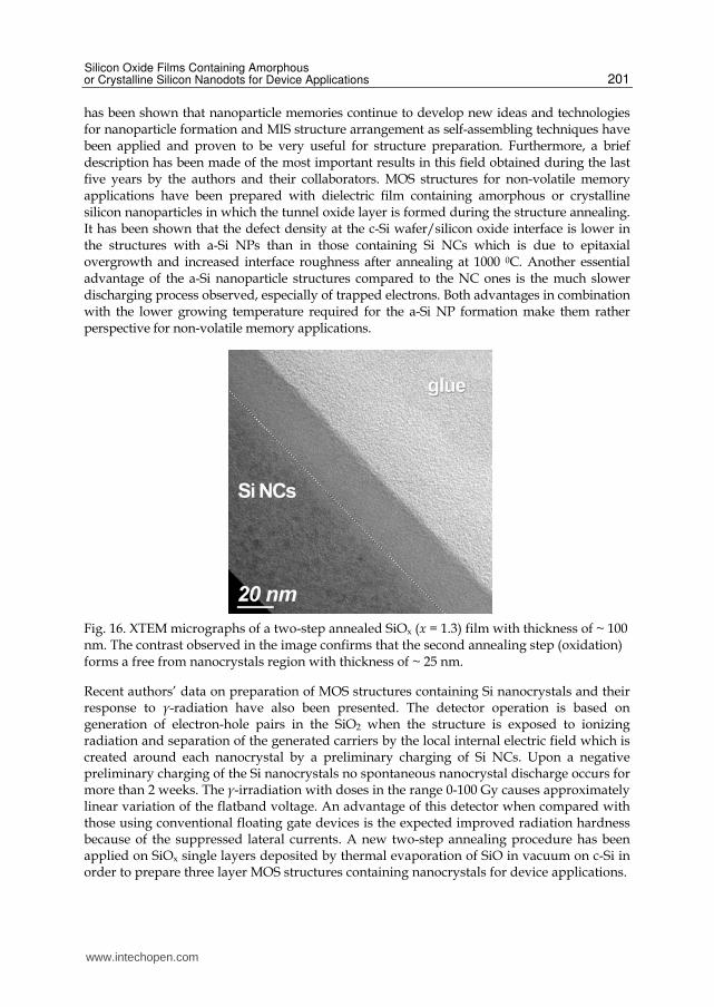
min N2 annealing. Figure 16 shows a XTEM micrograph of ~ 100 nm thick SiOx (x = 1.3) film
annealed for 50 min in pure N2 and then for 10 min in 90 % N2 + 10 % O2 atmosphere. It
proves that a two layer dielectric with ~ 75 nm SiO2-Si NCs region and ~ 25 nm SiO2 region
free from nanocrystals has been successfully produced.
MOS structures with multilayer gate dielectric containing NCs obtained by the new two-step annealing process are currently tested as radiation dosimeters and NVMs.
5. Conclusions
In this paper, we have reviewed some interesting results of other research groups on MIS structures containing Si nanocrystals for non-volatile memory and detector applications. It
www.intechopen.com
Silicon Oxide Films Containing Amorphous or Crystalline Silicon Nanodots for Device Applications
201
has been shown that nanoparticle memories continue to develop new ideas and technologies for nanoparticle formation and MIS structure arrangement as self-assembling techniques have been applied and proven to be very useful for structure preparation. Furthermore, a brief description has been made of the most important results in this field obtained during the last five years by the authors and their collaborators. MOS structures for non-volatile memory applications have been prepared with dielectric film containing amorphous or crystalline silicon nanoparticles in which the tunnel oxide layer is formed during the structure annealing. It has been shown that the defect density at the c-Si wafer/silicon oxide interface is lower in the structures with a-Si NPs than in those containing Si NCs which is due to epitaxial overgrowth and increased interface roughness after annealing at 1000 0C. Another essential advantage of the a-Si nanoparticle structures compared to the NC ones is the much slower discharging process observed, especially of trapped electrons. Both advantages in combination with the lower growing temperature required for the a-Si NP formation make them rather perspective for non-volatile memory applications.
Fig. 16. XTEM micrographs of a two-step annealed SiOx (x = 1.3) film with thickness of ~ 100 nm. The contrast observed in the image confirms that the second annealing step (oxidation) forms a free from nanocrystals region with thickness of ~ 25 nm.
Recent authors’ data on preparation of MOS structures containing Si nanocrystals and their response to γ-radiation have also been presented. The detector operation is based on generation of electron-hole pairs in the SiO2 when the structure is exposed to ionizing radiation and separation of the generated carriers by the local internal electric field which is created around each nanocrystal by a preliminary charging of Si NCs. Upon a negative preliminary charging of the Si nanocrystals no spontaneous nanocrystal discharge occurs for more than 2 weeks. The γ-irradiation with doses in the range 0-100 Gy causes approximately linear variation of the flatband voltage. An advantage of this detector when compared with those using conventional floating gate devices is the expected improved radiation hardness because of the suppressed lateral currents. A new two-step annealing procedure has been applied on SiOx single layers deposited by thermal evaporation of SiO in vacuum on c-Si in order to prepare three layer MOS structures containing nanocrystals for device applications.
www.intechopen.com

Quantum Dots – A Variety of New Applications
202
The above described authors’ results indicate that the developed techniques for MOS structures preparation based on thermal evaporation of SiO in vacuum are well suited for preparation of Si nanoparticle memories and radiation detectors. All processing steps including the thermal annealing required for Si NP formation are compatible with the contemporary CMOS technology. Follow-up experiments should take place in a production environment and focus on the integration of the methods in the technology of commercial memory and detector devices.
6. Acknowledgements
The authors are very grateful to all their collaborators who have taken part in the development of the MIS structures for memory and detector applications. The measurements were carried out in part in the Frederick Seitz Materials Research Laboratory Central Facilities, University of Illinois, which are partially supported by the U.S. Department of Energy under grants DE-FG02-07ER46453 and DE-FG02-07ER46471. The collaboration with the TEM Laboratory, CNyN, UNAM, of Dr. Oscar Contreras Lopez and especially with Francisco Ruiz Medina is also gratefully acknowledged.
7. References
Aktag, A., Yilmaz, E., Mogaddam, N.A.P., Aygun, G., Cantas, A. & Turan, R. (2010). Ge Nanocrystals Embedded in SiO2 in MOS Based Radiation Sensors. Nuclear Instruments and Methods in Physics Research, Section B-Beam Interactions with Materials and Atoms, Vol. 268, No. 22, pp 3417-3420, ISSN 0168-583X
Alfonsetti, R., Lozzi, L., Passacantando, M., Picozzi, P. & Santucci, S. (1993). XPS studies on SiOx thin films. Applied Surface Science, Vol. 70-71, No. 1, (June 1993), pp 222-225, ISSN 0169-4332
Buehler, M.G., Blaes, B.R., Soli, G.A. & Tardio, G.R. (1993). On-chip p-MOSFET dosimetry. IEEE Transactions on Nuclear Science, Vol. 40, No. 6, pp 1442-1449, ISSN 0018-9499
Carreras, J., Garrido, B. & Morante, J.R. (2005). Improved charge injection in Si nanocrystal non-volatile memories. Microelectronics Reliability, Vol. 45, (May - June, 2005), pp 899-902, ISSN 00262714
Claverie, A., Bonafos, C., Assayag, G.B., Schamm, S., Cherkashin, N., Paillard, V., Dimitrakis, P., Kapetenakis, E., Tsoukalas, D., Muller, T., Schmidt, B., Heinig, K.H., Perego, M., Fanciulli, M., Mathiot, D., Carrada, M. & Normand, P. (2006). Materials Science Issues for the Fabrication of Nanocrystal Memory Devices by Ultra Low Energy Ion Implantation. Journal Defect and Diffusion Forum, Vol. 258 - 260, (October, 2006 ), pp 531-541 ISSN 1662-9507
Curiel M., I. Petrov, N. Nedev, D. Nesheva, M. Sardela, Y. Murata, B. Valdez, E. Manolov, and I. Bineva, Formation of Si nanocrystals in thin SiO2 films for memory device applications, Materials Science Forum Vol. 644 (2010b) pp. 101-104, ISSN:0255-5476.
Curiel, M., Nedev, N., Nesheva, D., Soares, J., Haasch, R., Sardela, M., Valdez, B., Sankaran, B., Manolov, E., Bineva, I. & Petrov, I. (2010a). Microstructural characterization of thin SiOx films obtained by physical vapor deposition. Materials Science & Engineering B, Vol. 174, pp 132-136, ISSN 0921-5107
www.intechopen.com

Silicon Oxide Films Containing Amorphous or Crystalline Silicon Nanodots for Device Applications
203
Donchev, V., Nesheva, D., Todorova, D., Germanova, K. & Valcheva, E. (in press). Computer simulation study of infra-red transmission spectra of Si-SiOx nanocomposites. Thin Solid Films, ISSN 0040-6090
Edgecock, R., Matheson, J., Weber, M., Villani, E.G., Bose, R., Khan, A., Smith, D.R., Adil-Smith, I. & Gabrielli, A. (2009). Evaluation of commercial programmable floating gate devices as radiation dosimeters. Journal of Instrumentation, Vol. 4, (February 2009), pp P02002, ISSN 1748-0221
Eitan, B., Pavan, P., Bloom, I., Aloni, E., Frommer, A. & Finzi, D. (2000). NROM: a novel localized trapping, 2-bit nonvolatile memory cell. IEEE Electron Device Letters, Vol. 21, No. 11, pp 543-545, ISSN 0741-3106
Gerardi, C., Cester, A., Lombardo, S., Portoghese, R. & Wrachien, N. (2011). Nanocrystal Memories: An Evolutionary Approach to Flash Memory Scaling and a Class of Radiation-Tolerant Devices, In: Radiation effects in semiconductors, Iniewski, K., pp 103-150. CRC Press,Taylor&Francis Group. ISBN 9781439826942, Boca Raton
Han, K.I., Park, Y.M., Kim, S., Choi, S.-H., Kim, K.J., Park, I.H. & Park, B.-G. (2007). Enhancement of Memory Performance Using Doubly Stacked Si-Nanocrystal Floating Gates Prepared by Ion Beam Sputtering in UHV IEEE Transactions on Electron Devices, Vol. 54, No. 2, (Feb. 2007), pp 359 - 362, ISSN 0018-9383
Holmes-Siedle, A. & Adams, L. (1986). RADFETs: A Review of the Use of Metal Oxide Silicon Devices as Integrating Dosimeters. Radiation Physics and Chemistry, Vol. 28, No. 2, pp 235-244, ISSN 0969-806X
Horváth, Z.J. & Basa, P. (2009). Nanocrystal Non-Volatile Memory Devices. Materials Science Forum:Thin Films and Porous Materials, Vol. 609, (January, 2009), pp 1-9 ISSN 1662-9752
Hudgens, S. & Johnson, B. (2004). Overview of Phase-Change Chalcogenide Nonvolatile Memory Technology. MRS Bulletin, Vol. 29, pp 829-832, ISSN 0883-7694
Hughes, R.C., Huffman, D., Snelling, J.V., Zipperian, T.E., Ricco, A.J. & Kelsey, C.A. (1988). Miniature Radiation Dosimeter for in vivo Radiation Measurements. International Journal of Radiation Oncology Biology Physics, Vol. 14, pp 963-7, ISSN 0360-3016
Ioannou-Sougleridis, V., Nassiopoulou, A.G. & Travlos, A. (2003). Effect of high temperature annealing on the charge trapping characteristics of silicon nanocrystals embedded within SiO. Nanotechnology, Vol. 14, No. 11, pp 1174, ISSN 0957-4484
Iqbal, Z. & Veprek, S. (1982). Raman scattering from hydrogenated microcrystalline and amorphous silicon. Journal of Physics C: Solid State Physics, Vol. 15, pp 377-392, ISSN 0022-3719
Jung, J. & Cho, W.-J. (2008). Tunnel Barrier Engineering for Non-Volatile Memory. Journal of Semiconductor Technology and Science, Vol. 8, No. 1, pp 32-39, ISSN 1598-1657
Kassabov, J., Nedev, N. & Smirnov, N. (1991). Radiation dosimeter based on floating gate MOS transistor. Radiation Effects and Defects in Solids, Vol. 116, No. 1-2, pp 155-158, ISSN 1042-0150
Kouvatsos, D.N., Ioannou-Sougleridis, V. & Nassiopoulou, A.G. (2003). Charging effects in silicon nanocrystals within SiO2 layers, fabricated by chemical vapor deposition, oxidation, and annealing Applied Physics Letters, Vol. 82, No. 3, (15 January 2003), pp 397, ISSN 0003-6951
Liu, Y., Chen, T.P., Ng, C.Y., Ding, L., Zhang, S., Fu, Y.Q. & Fung, S. (2006). Depth Profiling of Charging Effect of Si Nanocrystals Embedded in SiO2: A Study of Charge
www.intechopen.com

Quantum Dots – A Variety of New Applications
204
Diffusion among Si Nanocrystals. Journal of Physical Chemistry B, Vol. 110, No. 33, (August 2, 2006), pp 16499-16502, ISSN 1520-5207
Lombardo, S., Corso, D., Crupi, I., Gerardi, C., Ammendola, G., Melanotte, M., De Salvo, B. & Perniola, L. (2004). Multi-bit storage through Si nanocrystals embedded in SiO2. Microelectronic Engineering, Vol. 72, pp 411-414, ISSN 0167-9317
Lu, T.Z., Alexe, M., Scholz, R., Talelaev, V. & Zacharias, M. (2005). Multilevel charge storage in silicon nanocrystal multilayers. Applied Physics Letters, Vol. 87, No. 20, (November 2005), ISSN 0003-6951
Lu, T.Z., Alexe, M., Scholz, R., Talalaev, V. & Zacharias, M. (2006). Si nanocrystal based memories: Effect of the nanocrystals density. Journal of Applied Physics, Vol. 100, pp 014310, ISSN 0003-6951
Martin, M.N., Roth, D.R., Garrison-Darrin, A., McNulty, P.J. & Andreou, A.G. (2001). FGMOS dosimetry: design and implementation. IEEE Transactions on Nuclear Science, Vol. 48, No. 6, pp 2050 - 2055, ISSN 0018-9499
McNulty, P.J., Poole, K.F., Crissler, M., Reneau, J., Cellere, G., Paccagnella, A., Visconti, A., Bonanomi, M., Stroebel, D., Fennell, M. & Perez, R. (2006). Sensitivity and dynamic range of FGMOS dosemeters. Radiation Protection Dosimetry, Vol. 122, No. 1-4, (March 26 2007 ), pp 460-2, ISSN 1742-3406
Minami, S.-i., Ujiie, K., Terasawa, M., Komori, K., Furusawa, K. & Kamigaki, Y. (1994). A 3 Volt 1 Mbit Full-Featured EEPROM Using a Highly-Reliable MONOS Device Technology. IEICE Transactions on Electronics, Vol. Vol.E77-C, No. 8, (August 20 1994), pp 1260-1269, ISSN 0916-8516
Nassiopoulou, A.G., Olzierski, A., Tsoi, E., Salonidou, A., Kokonou, M., Stoica, T. & Vescan, L. (2009). Laterally ordered 2-D arrays of Si and Ge nanocrystals within SiO2 thin layers for application in non-volatile memories International Journal of Nanotechnology, Vol. 6, No. 1/2, pp 18 - 34, ISSN 1741-8151
Nedev, N., Nesheva, D., Manolov, E., Brüggemann, R., Meier, S. & Levi, Z. (2008a). Memory Effect in MOS Structures Containing Amorphous or Crystalline Silicon Nanoparticles. Proceedings of 26th International Conference on Microelectronics (MIEL 2008), ISBN 978-1-4244-1881-7, Nis, Serbia, May 2008.
Nedev, N., Nesheva, D., Manolov, E., Brüggemann, R., Meier, S., Levi, Z. & Zlatev, R. (2008b). MOS structures containing silicon nanoparticles for memory device applications. Journal of Physics: Conference Series, Vol. 113, pp 012034, ISSN 1742-6596
Nedev, N., Manolov, E., Nesheva, D., Krezhov, K., Nedev, R., Curiel, M., Valdez, B., Mladenov, A. & Levi, Z. (2011). Radiation dosimeter based on Metal-Oxide-Semiconductor structures containing silicon nanocrystals. Key Engineering Materials (accepted), ISSN 1013-9826
Nesheva, D., Raptis, C., Perakis, A., Bineva, I., Aneva, Z., Levi, Z., Alexandrova, S. & Hofmeister, H. (2002). Raman scattering and photoluminescence from Si nanoparticles in annealed SiOx thin films. Journal of Applied Physics, Vol. 92, No. 8, pp 4678-4683, ISSN 0003-6951
Nesheva, D., Bineva, I., Levi, Z., Aneva, Z., Merdzhanova, T. & Pivin, J.C. (2003). Composition, structure and annealing-induced phase separation in SiOx films produced by thermal evaporation of SiOin vacuum. Vacuum, Vol. 68, pp 1-9, ISSN 0042-207X
www.intechopen.com

Silicon Oxide Films Containing Amorphous or Crystalline Silicon Nanodots for Device Applications
205
Nesheva, D., Nedev, N., Manolov, E., Bineva, I. & Hofmeister, H. (2007). Memory effect in MIS structures with amorphous silicon nanoparticles embedded in ultra thin SiOx matrix. Journal of Physics and Chemistry of Solids, Vol. 68, pp 725-728, ISSN 0022-3697
Nesheva, D., Nedev, N., Levi, Z., Brüggemann, R., Manolov, E., Kirilov, K. & Meier, S. (2008). Absorption and transport properties of Si rich oxide layers annealed at various temperatures. Semiconductor Science Technology, Vol. 23, (March 2008), pp 045015-8, ISSN 1361-6641
Ng, C.Y., Chen, T.P., Sreeduth, D., Chen, Q., Ding, L. & Du, A. (2006a). Silicon nanocrystal-based non-volatile memory devices. Thin Solid Films, Vol. 504, No. 1-2, pp 25-27, ISSN 0040-6090
Ng, C.Y., Chen, T.P., Yang, M., Yang, J.B., Ding, L., Li, C.M., Du, A. & Trigg, A. (2006b). Impact of programming mechanisms on the performance and reliability of nonvolatile memory devices based on Si nanocrystals. IEEE Transactions on Electron Devices, Vol. 53, No. 4 (March 27), pp 663 - 667, ISSN 0018-9383
Nicollian, E.H. & Brews, J.R. (2002). MOS (Metal Oxide Semiconductor) Physics and Technology, Wiley-Interscience, ISBN ISBN: 978-0-471-43079-7, New York
Normand, P., Tsoukalas, D., Kapetanakis, E., Berg, J.A.V.D., Armour, D.G., Stoemenos, J. & Vieude, C. (1998). Formation of 2-D Arrays of Silicon Nanocrystals in Thin SiO2 Films by Very-Low Energy Si+ Ion Implantation. Electrochemical and Solid-State Letters, Vol. 1, No. 2, (June 11, 1998), pp 88-90, ISSN 1099-0062
Normand, P., Kapetanakis, E., Dimitrakis, P., Tsoukalas, D., Beltsios, K., Cherkashin, N., Bonafos, C., Benassayag, G., Coffin, H., Claverie, A., Soncini, V., Agarwal, A. & Ameen, M. (2003). Effect of annealing environment on the memory properties of thin oxides with embedded Si nanocrystals obtained by low-energy ion-beam synthesis Applied Physics Letters, Vol. 83, No. 1, ISSN 0003-6951
Normand, P., Dimitrakis, P., Kapetanakis, E., Skarlatos, D., Beltsios, K., Tsoukalas, D., Bonafos, C., Coffin, H., Benassayag, G., Claverie, A., Soncini, V., Agarwal, A., Sohl, C. & Ameen, M. (2004). Processing issues in silicon nanocrystal manufacturing by ultra-low-energy ion-beam-synthesis for non-volatile memory applications. Microelectronic Engineering, Vol. 73-74, pp 730-735, ISSN 0167-9317
Oda, S., Huang, S.-Y., Salem, M.A. & Mizuta, H. (2005). Charge storage in silicon nanocrystals and device application. Proceedings of First Internantional Workshop on Semiconductor Nanocrystals, Seminano2005, ISBN 963 7371 20 6, ISBN 963 7371 18 4, Budapest, Hungary, September 2005.
Price, R.A., Benson, C., Joyce, M.J. & Rodgers, K. (2004). Development of a RADFET linear array for intracavitary in vivo dosimetry during external beam radiotherapy and brachytherapy. IEEE Transactions on Nuclear Science, Vol. 51, No. 4, (Aug. 2004), pp 1420-1426, ISSN 0018-9499
Ramani, R., Russell, S. & O'Brien, P.F. (1997). Clinical Dosimetry Using MOSFETS. International Journal of Radiation, Oncology, Biology, Physics, Vol. 37, No. 4, pp 959, ISSN 0360-3016
Rao, R.A., Steimle, R.F., Sadd, M., Swift, C.T., Hradsky, B., Straub, S., Merchant, T., Stoker, M., Anderson, S.G.H., Rossow, M., Yater, J., Acred, B., Harber, K., Prinz, E.J., White Jr, B.E. & Muralidhar, R. (2004). Silicon nanocrystal based memory devices for NVM and DRAM applications. Solid-State Electronics, Vol. 48, No. 9, pp 1463-1473, ISSN 0038-1101
www.intechopen.com

Quantum Dots – A Variety of New Applications
206
Sarrabayrouse, G. (1991 ). MOS radiation dosimeter: sensitivity and stability Proceedings of First European Conference on Radiation and its Effects on Devices and Systems, RADECS 91, ISBN 0-7803-0208-7, La Grande-Motte, France, 9-12 Sept. 1991
Scheick, L.Z., McNulty, P.J. & Roth, D.R. (1998). Dosimetry based on the erasure of floating gates in the natural radiation environments in space. IEEE Transactions on Nuclear Science, Vol. 45, No. 6, pp 2681 - 2688, ISSN 0018-9499
Scheick, L.Z., McNulty, P.J., Roth, D.R., Davis, M.G. & Mason, B.E. (1999). Measurements of dose with individual FAMOS transistors. IEEE Transactions on Nuclear Science, Vol. 46, No. 6, pp 1751 - 1756, ISSN 0018-9499
Stanic, S., Asano, Y., Ishino, H., Igarashi, A., Iwaida, S., Nakano, Y., Terazaki, H., Tsuboyama, T., Yoda, I. & ЕЅontar, D. (2005). Radiation monitoring in Mrad range using radiation-sensing field-effect transistors. Nuclear Instruments and Methods in Physics Research Section A: Accelerators, Spectrometers, Detectors and Associated Equipment, Vol. 545, No. 1-2, pp 252-260, ISSN 0168-9002
Steimle, R.F., Muralidhar, R., Rao, R., Sadd, M., Swift, C.T., Yater, J., Hradsky, B., Straub, S., Gasquet, H., Vishnubhotla, L., Prinz, E.J., Merchant, T., Acred, B., Chang, K. & Jr., B.E.W. (2007). Silicon nanocrystal non-volatile memory for embedded memory scaling. Microelectronics Reliability, Vol. 47, No. 4-5, (April-May 2007), pp 585-592, ISSN 0026-2714
Sze, S.M. (1981). Physics of Semiconductor Devices (2nd edition), Wiley, ISBN 0-471-05661-8, New York
Tarr, N.G., Mackay, G.F., Shortt, K. & Thomson, I. (1998). A floating gate MOSFET dosimeter requiring no external bias supply. IEEE Transactions on Nuclear Science, Vol. 45, No. 3, pp 1470 - 1474 ISSN 0018-9499
Tarr, N.G., Shortt, K., Wang, Y. & Thomson, I. (2004). A sensitive, temperature-compensated, zero-bias floating gate MOSFET dosimeter IEEE Transactions on Nuclear Science, Vol. 51, No. 3, pp 1277 - 1282, ISSN 0018-9499
Tiwari, S., Rana, F., Chan, K., Hanafi, H., Chan, W. & Buchanan, D. (1995). Volatile and non-volatile memories in silicon with nano-crystal storage. Proceedings of International Electron Devices Meeting, IEDM'95, ISBN 01631918 Washington, DC, USA, 10 -13 December 1995
Tiwari, S., Rana, F., Hanafi, H., Hartstein, A., Crabbe, E.F. & Chan, K. (1996). A silicon nanocrystals based memory. Applied Physics Letters, Vol. 68, No. 10, (April 1996), pp 1377-80, ISSN 0003-6951
Tsoi, E., Normand, P., Nassiopoulou, A.G., Ioannou-Sougleridis, V., Salonidou, A. & Giannakopoulos, K. (2005). Silicon nanocrystal memories by LPCVD of amorphous silicon, followed by solid phase crystallization and thermal oxidation Journal of Physics: Conference Series, Vol. 10, pp 31, ISSN 1742-6588
Tsoukalas, D., Dimitrakis, P., Kolliopoulou, S. & Normand, P. (2005). Recent advances in nanoparticle memories. Materials Science and Engineering: B, Vol. 124-125, pp 93-101, ISSN 0921-5107
Yu, Z., Aceves, M., Carrillo, J. & Flores, F. (2003). Single electron charging in Si nanocrystals embedded in silicon-rich oxide Nanotechnology, Vol. 14, No. 9, pp 959, ISSN 0957-4484
www.intechopen.com

Quantum Dots - A Variety of New ApplicationsEdited by Dr. Ameenah Al-Ahmadi
ISBN 978-953-51-0483-4Hard cover, 280 pagesPublisher InTechPublished online 04, April, 2012Published in print edition April, 2012
InTech EuropeUniversity Campus STeP Ri Slavka Krautzeka 83/A 51000 Rijeka, Croatia Phone: +385 (51) 770 447 Fax: +385 (51) 686 166www.intechopen.com
InTech ChinaUnit 405, Office Block, Hotel Equatorial Shanghai No.65, Yan An Road (West), Shanghai, 200040, China
Phone: +86-21-62489820 Fax: +86-21-62489821
The book “Quantum dots: A variety of a new applications” provides some collections of practical applications ofquantum dots. This book is divided into four sections. In section 1 a review of the thermo-opticalcharacterization of CdSe/ZnS core-shell nanocrystal solutions was performed. The Thermal Lens (TL)technique was used, and the thermal self-phase Modulation (TSPM) technique was adopted as the simplestalternative method. Section 2 includes five chapters where novel optical and lasing application are discussed.In section 3 four examples of quantum dot system for different applications in electronics are given. Section 4provides three examples of using quantum dot system for biological applications. This is a collaborative booksharing and providing fundamental research such as the one conducted in Physics, Chemistry, Biology,Material Science, Medicine with a base text that could serve as a reference in research by presenting up-to-date research work on the field of quantum dot systems.
How to referenceIn order to correctly reference this scholarly work, feel free to copy and paste the following:
Diana Nesheva, Nikola Nedev, Mario Curiel, Irina Bineva, Benjamin Valdez and Emil Manolov (2012). SiliconOxide Films Containing Amorphous or Crystalline Silicon Nanodots for Device Applications, Quantum Dots - AVariety of New Applications, Dr. Ameenah Al-Ahmadi (Ed.), ISBN: 978-953-51-0483-4, InTech, Available from:http://www.intechopen.com/books/quantum-dots-a-variety-of-new-applications/silicon-oxide-films-containing-amorphous-or-crystalline-silicon-nanodots-for-device-applications

© 2012 The Author(s). Licensee IntechOpen. This is an open access articledistributed under the terms of the Creative Commons Attribution 3.0License, which permits unrestricted use, distribution, and reproduction inany medium, provided the original work is properly cited.