Embed Size (px)
Citation preview

Simulating Power Supplies with SPICE

www.onsemi.com2
AgendaWhy simulating power supplies?Average modeling techniquesThe PWM switch concept, CCMThe PWM switch concept, DCMThe voltage-mode model at workCurrent-mode modelingThe current-mode model at workPower factor correctionSwitching modelsEMI filteringConclusion

www.onsemi.com3
AgendaWhy simulating power supplies?Average modeling techniquesThe PWM switch concept, CCMThe PWM switch concept, DCMThe voltage-mode model at workCurrent-mode modelingThe current-mode model at workPower factor correctionSwitching modelsEMI filteringConclusion

www.onsemi.com4
Simulation helps feeling how the product behaves before breadboardExperiment What If? at any level. Power libraries do not blow!Easily shows impact of parameter variations: ESR, Load etc.Draw Bode plots without using costly equipmentsAvoid trials and errors: compensate the loop on the PC first!Use SPICE to assess current amplitudes, voltage stresses etc.Go to the lab. and check if the assumptions were valid.
Why Simulate Switch Mode Power Supplies?
SPICE does NOTNOT replace the breadboard!
SPICE
Calm down!

www.onsemi.com5
An average model is made of equations that are continuous in timeThe switching component has disappeared, leading to:a simpler ac analysis of the power supplythe study of the stability margins in various conditionsthe assessment of the ESRs contributions in the loop stabilitya flashing simulation time!
Why AverageAverage Simulations?
Averagemodeling
1
Rload3
5
Resr100m
Cout220uF
2
VgAC = 0
Vout
4
DutyV2AC = 1
3
Vin Vout
Gnd Ctrl
AC model
DRS = 20mFS = 50kVOUT = 5RL = 3VIN = 11X1RI = 0.33L = 37.5u
0
0
0
0.458 0

www.onsemi.com6
An switching model is like breadboarding on the PCThe switching component is back in place, leading to:the analysis of current and voltage stressesthe study of leakage and stray elements impactsthe analysis of the input current signature – EMIa longer simulation time…
Why SwitchingSwitching Simulations?
Switchingapproach
1 vout 2 il
3.50
4.50
5.50
6.50
7.50
vout
in v
olts
Plot
1 1
50.0u 150u 250u 350u 450utime in seconds
600m
1.00
1.40
1.80
2.20
il in
am
pere
sPl
ot2
2
7
4
10
1
6
2
14
123
8
19
5
15
RESR_C30.3702
C2100UIC = 11.9999
C3220u/DIVIC = 230
C41n
R_X2_SEC13M
D5DN4934
C50.68u/DIVIC = 0
RLOAD657
D6MUR130
R4100K
R522K
R81.0MEG
L_X2_PR320U
R911K
R_X2_PR0.162
R100.1
X3MTP8N50
VOUTVCC Vsw
Zero_CD
CS * Pout
I_LOAD
Vdrv
FB
CTRL
Ct
CS ZCD
GND
DRV
Vcc
X1Config_1
VCTRL

www.onsemi.com7
AgendaWhy simulating power supplies?Average modeling techniquesThe PWM switch concept, CCMThe PWM switch concept, DCMThe voltage-mode model at workCurrent-mode modelingThe current-mode model at workPower factor correctionSwitching modelsEMI filteringConclusion

www.onsemi.com8
Average Modeling, the SSAStateState--SpaceSpace AveragingAveraging (SSA)Introduced by Slobodan Ćuk in the 80’Long and painful processFails to predict sub-harmonic oscillations
uL
xLdt
dx 1211+−=
2.
1112 xCoutRload
xCoutdt
dx−=
211 xLdt
dx−=
2.
1112 xCoutRload
xCoutdt
dx−=
VoutL
C R
x1
x2u1
VoutL
C R
x1
x2
offon
Apply smoothing process Linearize
Pfffff!ON OFF

www.onsemi.com9
Average Modeling, the PWM SwitchThe PWM SwitchPWM SwitchIntroduced by Vatché Vorpérian in the mid-80’Easy to derive and fully invariantNo auto-toggling mode modelsCan predict sub-harmonic oscillations in CCMDCM model in current-mode was never published!
ca
p
d
d'
Ia(t) Ic(t)
Vap(t) Vcp(t)
a c
PWM switch p
d
d'
Vin
L
C R Vout

www.onsemi.com10
The PWM Switch Concept
Vin
L
C R Voutac
PW
M s
witc
hp
d
d'
Linear network
Linear network
off
on
diode + transistor = guilty for non-linearity!
Identify the guilty network: the transistor and the diodeAverage their voltage and current waveforms: large-signal modelLinearize the equations around a dc point: small-signal model

www.onsemi.com11
AgendaWhy simulating power supplies?Average modeling techniquesThe PWM switch concept, CCMThe PWM switch concept, DCMThe voltage-mode model at workCurrent-mode modelingThe current-mode model at workPower factor correctionSwitching modelsEMI filteringConclusion

www.onsemi.com12
The PWM Switch Concept
1
4
2
Q1
5
Rb_upper1Meg
Rb_lower100k
Vg
Vout
8
3
7
h11 Beta.Ib
Rc10k
Re150
Ce1nF
ReqRb_upper//Rb_lower
b c
e
ib ic
ie
VinRc10k
Re150
Ce1nF
Vin
Vout
Ve
Remember the bipolarsEbers-Moll model…
Replace Q1 by its small-signal model
The transistor is a highly non-linear device:Replace the transistor with its small-signal modelSolve a system of linear equations

www.onsemi.com13
The PWM Switch Concept
a c
PWM switch p
d
d'
Vin
L
C R Vout
Vin
L
C R Voutac
PW
M s
witc
hp
d
d'
Vin
LC R Vout
ac
PWM
sw
itch
p
d
d'
ca
p
d
d'
Ia(t) Ic(t)
Vap(t) Vcp(t)BuckBuck
BoostBoostBuckBuck--boostboost
The PWM switch model works in all two switch converters:Rotate the model to match the switch and diode connectionsSolve a system of linear equations

www.onsemi.com14
The PWM Switch Concept
ca
p
d
d'
Ia(t) Ic(t)
Vap(t) Vcp(t)Vin
L
C RVout
0
1( ) ( ) ( )sw
sw sw
T
a a a c cT Tsw
I t I I t dt d I t dIT
= = = =∫0
1( ) ( ) ( )sw
sw sw
T
cp cp cp ap apT Tsw
V t V V t dt d V t dVT
= = = =∫
The keyword with average modeling: waveforms averaging

www.onsemi.com15
The PWM Switch Concept
ca
p
Ia(t) Ic(t)
V=d.V(a,p)
p
I=d.Ic
Large-signal (non-linear) model
The obtained set of equations is that of a transformerA CCM two-switch DC-DC can be modeled like a 1:D transformer!
V1 V2
I1 I21:N
2 1V NV=
1 2I NI=
ca
p
Ia(t) Ic(t)
1 dVap Vcp

www.onsemi.com16
The PWM Switch Concept
Ld
100uH
Vbias0.4AC = 1
C1100u
R110
Vout
Vin10
a
cp10.0 10.0
16.7
0.400
Always verify the dc operating point!
SPICE only deals with linear equationsIt first computes a bias point then it linearizes the network
1 10 100 1k 10k 100k
-30.0
-10.0
10.0
30.0
50.0
123
4
d = 40%, Vout = 16.7 V
d = 10%, Vout = 11.1 V
dB
( )( )
outV sd s
No equations, result appears in a second!Make sure the bias point is correct…

www.onsemi.com17
The PWM Switch ConceptWe have a set of non-linear equations: can’t derive transfer functions!We need a small-signal model: linearize the equations by handtwo options: perturbation or partial derivatives…
Pertubation Partial derivatives
0
0
0
ˆ
ˆ
ˆ
a c
a a a
c c c
I dI
I I i
I I i
d d d
=
= +
= +
= +
0
0
ˆˆ
cp ap
cp cp cp
V dV
V V v
d d d
=
= +
= +
( )( )0 0 0ˆˆ ˆ
a a c cI i d d I i+ = + +
0 0 0
0 0ˆˆ ˆ
a c
a c c
I d I
i d i dI
=
= +ac and dcequations
ˆˆ ˆ
a c
a aa c
c
I dII Ii i dI d
=∂ ∂
= +∂ ∂
ˆˆ ˆ
cp ap
cp cpcp ap
ap
V dV
V Vv v d
V d
=
∂ ∂= +∂ ∂
0 0ˆˆ ˆ
a c ci d i dI= +
0 0 0
0 0ˆˆ ˆ
cp ap
cp ap ap
V d V
v d v dV
=
= +
same
0 0ˆˆ ˆcp ap apv d v dV= +
ac equationsNo dc point

www.onsemi.com18
The PWM Switch ConceptPut the small-signal sources in the large-signal modelYou obtain the small-signal model of the CCM PWM switch
a c
p
0 0 0
0 0ˆˆ ˆ
cp ap
cp ap ap
V d V
v d v dV
=
= +
( )0ˆ
apV d d
0 ˆap apV v+
0ˆ
c cI i+
1V0 0cd I
( )0ˆ ˆ
c cd I i+
You can now analytically find the dc bias and the ac response!

www.onsemi.com19
AgendaWhy simulating power supplies?Average modeling techniquesThe PWM switch concept, CCMThe PWM switch concept, DCMThe voltage-mode model at workCurrent-mode modelingThe current-mode model at workPower factor correctionSwitching modelsEMI filteringConclusion

www.onsemi.com20
The PWM Switch in DCM
ca
p
d1
d2
Ia(t) Ic(t)
Vap(t) Vcp(t)Vin
L
C RVout
d3
IaIpeak
Vap
Ipeak
Ic
VcpVap
Vcp
d1Tsw d2Tsw d3Tsw
t
t
t
t
IaIpeak
Vap
Ipeak
Ic
VcpVap
Vcp
d1Tsw d2Tsw d3Tsw
t
t
t
t
3rd event linked to DCM
The original model could not be auto-togglingA new DCM-CCM model has been derived
( )
( )
1
1 2
1 2
1
2
2
peaka
peakc
c a
I dI
I d dI
d dI I
d
=
+=
+=
Extract andreplace

www.onsemi.com21
The PWM Switch in DCM
ca
p
Ia(t) Ic(t)
1 NVap Vcp
N=d1/(d1+d2)
12 1
1 1
2 ² 2c ac sw sw c
ac sw ac
I L V d T LF Id dV d T d V−
= = −Model input
Clamp d2:d2 CCM = 1- d1
d2 DCM = 1- d1- d3
d2 < 1 - d1model is in DCM!
By clamping the d2 equation, the circuit toggles between the modes

www.onsemi.com22
AgendaWhy simulating power supplies?Average modeling techniquesThe PWM switch concept, CCMThe PWM switch concept, DCMThe voltage-mode model at workCurrent-mode modelingThe current-mode model at workPower factor correctionSwitching modelsEMI filteringConclusion

www.onsemi.com23
The PWM Switch in DCM
3
V410
4
L175u
17d
a c
PWM switch VM p
X4PWMCCMVM
GAI
N
XPWMGAINK = 0.5
10.0
5.00
0.500
In voltage-mode, the duty-cycle is built with a ramp generatorThe transition occurs when the error voltage crosses the ramp
( ) ( ) ( )onerr peak peak
sw
t tV t V V d t
T= =
Vpeak
0
Verr
0
Vramp(t)
d(t)
ton
Tsw
( ) ( )err
peak
V td t
V=
( )( )
1PWM
err peak
d td Kd V t V⎛ ⎞
= =⎜ ⎟⎜ ⎟⎝ ⎠
Vpeak = 2 V

www.onsemi.com24
The Voltage-Mode Model at WorkLet us compensate a buck converter operated in CCM and DCM
1. Run an open-loop Bode plot at full load, lowest input2. Identify the excess/deficiency of gain at the selected cross over3. Place a double zero at f0, a pole at the ESR zero and a pole at Fsw/24. Check final loop gain and run a transient load test
Vout2
16
Cout220u
Resr150m
2 13
L1180u
6
Rupper38k
Rlower10k
9
5
X2AMPSIMP
V22.5
vout
d
a c
PWM switch VM p
4
7
X3PWMVML = 180uFs = 100kG
AIN
15
XPWMGAINK = 0.4
R420m
LoL1kH
10
CoL1kF
V1AC = 1
Vin
vout
Vout
12
R2R2
C1C1
C2C2
8
R3R3
C3C3
Rload3
Vin20
12.0V
12.0V
12.0V
2.50V
2.50V
1.51V
20.0V
12.1V
604mV
1.51V
1.51V 12.0V
parameters
Rupper=38kfc=7kGfc=-15
G=10^(-Gfc/20)pi=3.14159
fz1=650fz2=650fp1=7kfp2=50k
C3=1/(2*pi*fz1*Rupper)R3 =1/(2*pi*fp2*C3)
C1=1/(2*pi*fz2*R2)C2=1/(2*pi*(fp1)*R2)
a=fc^4+fc^2*fz1^2+fc^2*fz2^2+fz1^2*fz2^2c=fp2^2*fp1^2+fc^2*fp2^2+fc^2*fp1^2+fc^4
R2=sqrt(c/a)*G*fc*R3/fp1
Automatedcompensation
H(s)
T(s)

www.onsemi.com25
The Voltage-Mode Model at Work
-24.0
-12.0
0
12.0
24.0
-180
-90.0
0
90.0
180
2
1
10 100 1k 10k 100k
-180
-90.0
0
90.0
180
-40.0
-20.0
0
20.0
40.0
3
4
Pm = 80°
fc = 7 kHz
|H(7 kHz)| =-15 dB
Arg H(7 kHz) =-121°
Arg T(s)
|H(s)|
9.91m 11.0m 12.1m 13.3m 14.4m
11.6
11.8
12.0
12.2
12.4
12
The Bode plot reveals a gain loss of -15 dB at 7 kHzThe compensator provides a +15 dB gain increase plus phase boost
The final loop gain shows a comfortable phase marginThe transient response at both input levels shows a stable signal
|T(s)|
arg|H(s)|
Vout(t)
Iout = 200 mA to 4 Ain 10 µs

www.onsemi.com26
AgendaWhy simulating power supplies?Average modeling techniquesThe PWM switch concept, CCMThe PWM switch concept, DCMThe voltage-mode model at workCurrent-mode modelingThe current-mode model at workPower factor correctionSwitching modelsEMI filteringConclusion

www.onsemi.com27
Current-Mode OperationIn voltage-mode, the error signal directly controls the duty cycleIn current mode, the error voltage sets the inductor peak currentTo derive a model, observe the current signals and average them!
'( )( ) ( ) ( )
2
(1 )2
f swc i c sw e
c sw e swc cp
i i
S d t TI t R V t d t T S
V T S TI d V dR R L
= − −
= − − −
1 2
3
ca
p
Ia(t) Ic(t)
I=Vc/Ri
p
I=d.Ic I=Iu Cs
'( )( ) ( ) ( )
2
(1 )2
f swc i c sw e
c sw e swc cp
i i
S d t TI t R V t d t T S
V T S TI d V dR R L
= − −
= − − −
1 2
3
ca
p
Ia(t) Ic(t)
I=Vc/Ri
p
I=d.Ic I=Iu Cs
1
2
3
CCM

www.onsemi.com28
Current-Mode OperationDo the same for DCM signalsMatch the previous structure to build a CCM/DCM model
ca
p
Ia(t) Ic(t)
I=Vc/Ri
p
I=(d1/(d1+d2)).Ic I=Iu
3rd event linked to DCM
1
12
1 1 22 1
2
c sw epeak
i
c sw ec sw f
i
cpsw esw
i
V d T SIR
V d T SI d T SR
Vd T S d dI d TR Lμ
α
−=
−= −
+⎛ ⎞= + −⎜ ⎟⎝ ⎠
α
DCM

www.onsemi.com29
AgendaWhy simulating power supplies?Average modeling techniquesThe PWM switch concept, CCMThe PWM switch concept, DCMThe voltage-mode model at workCurrent-mode modelingThe current-mode model at workPower factor correctionSwitching modelsEMI filteringConclusion

www.onsemi.com30
The Current-Mode Model at WorkTo study a converter, we can write down the equationsOr use a SPICE simulation to get the Bode plot in a secondTake the example of a current-mode flyback converter
( ) 2
1
2 22
1 3
10 0 2 2 22
1 1 1120log
1 1
z z z
p n n p
f f ff f f
H f Gf f ff f f Q
⎡ ⎤⎛ ⎞ ⎛ ⎞⎛ ⎞⎢ ⎥
+ + +⎜ ⎟ ⎜ ⎟⎜ ⎟⎢ ⎥⎜ ⎟⎝ ⎠ ⎝ ⎠⎝ ⎠⎢ ⎥= ⎢ ⎥⎛ ⎞ ⎛ ⎞ ⎛ ⎞⎢ ⎥⎛ ⎞+ ⎜ ⎟ ⎜ ⎟− + ⎜ ⎟⎜ ⎟⎢ ⎥⎜ ⎟ ⎜ ⎟⎜ ⎟⎝ ⎠⎝ ⎠ ⎝ ⎠⎢ ⎥⎝ ⎠⎣ ⎦
( )1 2 3 1
1 1 1 1 12
1arg tan tan tan tan tan
1z z z p n p
n
f f f f fH ff f f f f Q f
f
− − − − −
⎛ ⎞⎜ ⎟
⎛ ⎞⎛ ⎞ ⎛ ⎞ ⎛ ⎞ ⎜ ⎟= − + − −⎜ ⎟⎜ ⎟ ⎜ ⎟ ⎜ ⎟ ⎜ ⎟⎜ ⎟ ⎜ ⎟ ⎜ ⎟⎜ ⎟ ⎛ ⎞⎝ ⎠ ⎝ ⎠ ⎝ ⎠⎝ ⎠ ⎜ ⎟− ⎜ ⎟⎜ ⎟⎝ ⎠⎝ ⎠

www.onsemi.com31
Stabilizing a CCM Flyback ConverterCapture a SPICE schematic with an averaged model
1
C56600u
R1014.4m
2Vin90AC = 0
3 4
X2xXFMRRATIO = -0.25 vout
vout
6DC
8
13
L1Lp
D1Ambr20200ctp
B1Voltage
V(errP)/3 > 1 ?1 : V(errP)/3
Rload4
vcac
PW
M s
witc
h C
Mp
duty
-cyc
le
X9PWMCML = LpFs = 65kRi = 0.25Se = 0
19.0V
19.0V
90.0V
-78.8V 19.7V
467mV
0V
786mV
Look for the bias points values: Vout = 19 V, okVsetpoint < 1 V, enough margin on current sense

www.onsemi.com32
Stabilizing a CCM Flyback ConverterCapture a SPICE schematic with an averaged model
18
Verr
Cpole2Cpole
109
11
vout
X8OptocouplerFp = PoleCTR = CTR
Czero1Czero
RpullupRpullup
5
RledRled
Rlower2Rlower
Rupper2Rupper
X10TL431_G
Vdd5
errP
X4POLEFP = poleK = 1
K
S+A
R71
err
14
LoL1kH
VstimAC = 1
15
CoL1kF
2.36V
0V
2.36V
2.36V
2.36V 18.7V
2.49V
17.7V
5.00V
parameters
Vout=19Ibridge=250uRlower=2.5/IbridgeRupper=(Vout-2.5)/IbridgeLp=350uSe=20kfc=1kpm=60Gfc=-22pfc=-71G=10^(-Gfc/20)boost=pm-(pfc)-90pi=3.14159K=tan((boost/2+45)*pi/180)Fzero=fc/kFpole=k*fcRpullup=20kRLED=CTR*Rpullup/GCzero=1/(2*pi*Fzero*Rupper)Cpole=1/(2*pi*Fpole*Rpullup)CTR=1.5Pole=6k
fromBode

www.onsemi.com33
Stabilizing a CCM Flyback ConverterCapture a SPICE schematic with an averaged model
-32.0
-16.0
0
16.0
32.0
4
10 100 1k 10k 100k
-180
-90.0
0
90.0
180
6
Gain at 1 kHz-22 dB
Phase at 1 kHz-71 °
|H(s)|
argH(s)
Sub harmonicpoles
Inject rampcompensation
ramp

www.onsemi.com34
Stabilizing a CCM Flyback ConverterThe easiest way to damp the poles:Calculate the equivalent quality coefficient at Fsw/2Calculate the external ramp to make Q less than 1
( )1 1 8
3.14 0.5 0.461'2
e
n
QSD DS
π= = =
× −⎛ ⎞+ −⎜ ⎟
⎝ ⎠
( )1 1 90 0.25 10.5 0.5 0.5 0.46 36
' ' 320 1 0.46 3.14n in i
ep
S V RS D D kV sD L D uπ π
×⎛ ⎞ ⎛ ⎞ ⎛ ⎞= − + = − + = − + =⎜ ⎟ ⎜ ⎟ ⎜ ⎟× −⎝ ⎠ ⎝ ⎠ ⎝ ⎠
NCP1230internal
Rramp
Ri
2.3 Vpp
18 kΩ
CS
DRV 2.3 15315rampS kV s
u= =
36 51%70
er
n
S kMS k
= = =
0.51 70 18 4.1153
r n rampcurrent
ramp
M S R k kR kS k
× ×= = = Ω
Rcurrent
On-time slope in i
p
V RL

www.onsemi.com35
Stabilizing a CCM Flyback ConverterBoost the gain by +22 dB, boost the phase at fc
11
-80.0
-40.0
0
40.0
80.0
10
10 100 1k 10k 100k
-180
-90.0
0
90.0
180
11
|T(s)|
argT(s)
Cross over1 kHz
Margin at 1 kHz60°
GM20 dB

www.onsemi.com36
Stabilizing a CCM Flyback ConverterTest the response at both input levels, 90 and 265 VrmsSweep ESR values and check margins again
1.80m 5.40m 9.00m 12.6m 16.2mtime in seconds
18.79
18.87
18.95
19.03
19.11
1211
Vout(t)
Lowline
Hiline
112 mV

www.onsemi.com37
AgendaWhy simulating power supplies?Average modeling techniquesThe PWM switch concept, CCMThe PWM switch concept, DCMThe voltage-mode model at workCurrent-mode modelingThe current-mode model at workPower factor correctionSwitching modelsEMI filteringConclusion
www.onsemi.com38
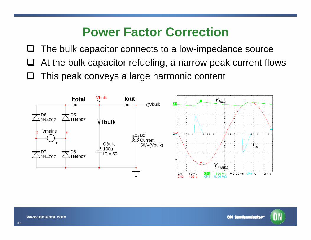
Power Factor Correction
CBulk100uIC = 50
6
D51N4007
2
D61N4007
D71N4007
D81N4007
Vmains
VbulkVbulk
B2Current50/V(Vbulk)
IoutItotal
Ibulk
Vbulk
Vmains
Iin
Vbulk
Vmains
Iin
The bulk capacitor connects to a low-impedance sourceAt the bulk capacitor refueling, a narrow peak current flowsThis peak conveys a large harmonic content

www.onsemi.com39
Power Factor Correction
Cbulk
D1 D2
D3 D4
Mains
PWM
VbulkPFCPre-converter
store release
Cbulk
D1 D2
D3 D4
Mains
PWM
VbulkPFCPre-converter
store release
A pre-converter is installed as a front-end sectionThe pre-converter draws a sinusoidal currentThe energy is stored and released in/by the bulk capacitor

www.onsemi.com40
Power Factor Correction
+
-
2
1
4
+-
177
3
5
16
118
Rlimit
Ddmg
12
Dout
Cout
VoutS
R
Q
Q 6
Verr
Reset detector
Rsense
current sensecomparator
9
10
13
G1A
B
K*A*B14
X6
C1
Vref
Rupper
Rlower
RdivL
RdivU18
D3
15
D4
D5D6
CinVin
Vdem
L
Peak currentsetpoint
Error amplifier
One of the most popular techinique uses Borderline modeThe MC33262 operates in peak current mode control
The NCP1606 also operates in constant-on time

www.onsemi.com41
Power Factor Correction
the averageaverage inductor current is halfhalf the inductor peak current value
8.05m 8.15m 8.25m 8.35m 8.45mtime in seconds
IL(t)
IL,peak
IL,avg
ton
IL = 0
( ) ( )( )sw
L inTI t t I t=
8.05m 8.15m 8.25m 8.35m 8.45mtime in seconds
IL(t)
IL,peak
IL,avg
ton
IL = 0
( ) ( )( )sw
L inTI t t I t=
The core is always reset from cycle to the other
On timeis constant

www.onsemi.com42
Power Factor Correction
4
9C5150uIC = Vrms*1.414
R1050m
16 23
L1L
parameterVrms=100Pout=150Vout=400Ri=0.22L=850u
5Vton
26Vfsw
22
13
17
G1100u
V42.5
25
C20.68u
R51G
Verr
14
V51.7
D2N = 0.01
15
D1N = 0.01
V36.4
10
R11.6Meg
R212k C3
10n
A
B
K*A*B
24
2
K = 0.6
R6100m
V11B1Current
I(V11) > 10u ? 10u : I(V11)
R310k
R41.6Meg
R823k
err
B4VoltageV(err)-2.05 < 0 ? 0 : V(err)-2.05
B1 3 0 V = V(1) * V(2) * K>1.3 ? 1.3 : V(1) * V(2) * K
vcac
PWM
sw
itch
BCM
p
ton
Fsw
(kH
z)
X5PWMBCMCM2L = LRi = Ri
3
6
VinVRMS
+
-
IN
8
X1KBU4J
Iin
ΔVin
Vrect
Cin1u
Vmul
Vout
RloadVout*Vout/Pout
A 150 W BCM PFC average example with the MC33262
Current-modeborderline model

www.onsemi.com43
Power Factor Correction
-8.00
-4.00
0
4.00
8.00vt
on in
vol
ts
-2.00
-1.00
0
1.00
2.00
iin in
am
pere
sP
lot1
1
3
394
398
402
406
410
vout
, vou
t#a
in v
olts
Plo
t2
62
1.139 1.149 1.159 1.169 1.179time in seconds
-60.0
-30.0
0
30.0
60.0
vton
in v
olts
-4.00
-2.00
0
2.00
4.00
iin in
am
pere
sP
lot3
4
5
THD = 2%
THD = 10% Iin(t)
Iin(t)
Vin = 230 Vac
Vin = 100 Vac
ton(t) - µs
ton(t) - µs
Vout,peak = 406 V
Vout,valley = 398 V Vout(t)
Highline
Lowline
Constanton-time
Average models can also work in transient conditions

www.onsemi.com44
Power Factor Correction
-80.0
-40.0
0
40.0
80.0ga
in in
db(
volts
)
-180
-90.0
0
90.0
180
phas
e in
deg
rees
plot
1
1
2
1m 10m 100m 1 10 100 1k 10k 100kfrequency in hertz
-80.0
-40.0
0
40.0
80.0
gain
in d
b(vo
lts)
-180
-90.0
0
90.0
180
phas
e in
deg
rees
Plo
t2
4
5
No zero added
Zero added
phase
gain
phase
gain
fc = 5 Hz
fc = 5 Hz
Pm = 61°
-80.0
-40.0
0
40.0
80.0ga
in in
db(
volts
)
-180
-90.0
0
90.0
180
phas
e in
deg
rees
plot
1
1
2
1m 10m 100m 1 10 100 1k 10k 100kfrequency in hertz
-80.0
-40.0
0
40.0
80.0
gain
in d
b(vo
lts)
-180
-90.0
0
90.0
180
phas
e in
deg
rees
Plo
t2
4
5
No zero added
Zero added
phase
gain
phase
gain
fc = 5 Hz
fc = 5 Hz
Pm = 61°
Use the model to boost the phase at the cross over point

www.onsemi.com45
Power Factor Correction
122m 365m 608m 851m 1.09time in seconds
320
350
380
410
440vo
ut#a
, vou
t#a#
1 in
vol
tsP
lot1
32
1.128 1.135 1.142 1.149 1.157time in seconds
-800m
-400m
0
400m
800m
iin, i
in#1
in a
mpe
res
Plo
t2
41
Vout(t)
Iin(t)
440 V
413 V
THD = 1.5%
THD = 10%
122m 365m 608m 851m 1.09time in seconds
320
350
380
410
440vo
ut#a
, vou
t#a#
1 in
vol
tsP
lot1
32
1.128 1.135 1.142 1.149 1.157time in seconds
-800m
-400m
0
400m
800m
iin, i
in#1
in a
mpe
res
Plo
t2
41
Vout(t)
Iin(t)
440 V
413 V
THD = 1.5%
THD = 10%
Added zero
No zero
Added zero
No zero
The zero improves the overshoot but degrades the THD…

www.onsemi.com46
AgendaWhy simulating power supplies?Average modeling techniquesThe PWM switch concept, CCMThe PWM switch concept, DCMThe voltage-mode model at workCurrent-mode modelingThe current-mode model at workPower factor correctionSwitching modelsEMI filteringConclusion

www.onsemi.com47
4
5
1 2
D11N5818
3Cout100uF
Resr100m Rload
10
Vout
Lp1mH
7
Rs100m
6
Lleak10uH
9
Vinput300V
Pulsegenerator
1:NOhmic losses
Primaryinductance
Leakageinductance
Capacitorparasitics
Switching Models, the Breadboard on PCTurn your PC into a virtual breadboard

www.onsemi.com48
Switching Models, the Breadboard on PC
18
Rsense2.8
12
6
R3200m
L23.5mH
1
9
R4100m
C1470uFIC = 5.5
Vout
IprimIripple1
L580uH
Vdrain
10
IDrain
Vsense
19
R15470
4
X1XFMRRATIO = -0.08
Rload13.4
15
X4MOC8101
Vinput126
13
Drv
VFB
31
L12.2uH
17
R1610m
32
R17300m
C210uF
IsecVsec
23 Cvcc10uFIC = 11.99
5 Vcc
16
Istartup
8Vadj
vout
Iout
R5100m
D1MBR140P
C3150p
14X3TL431
R214k
R710k
vout
C5100nFIC = 2.5
1
2
3
4 5
8
6
7
NCP1200
X5NCP1200
X2MTD1N60E
Primary inductance
Leakage inductance
Wire your device as you would do in the lab.

www.onsemi.com49
Simulations (Really) Work!!
505.00U 515.00U 525.00U 535.00U 545.00U
0
Vdrain100V/div
Vsense500mV/div
Assess the average, rms currents in your circuit Check if enough margins exist on your semiconductors
Leakageeffects
simulated measured
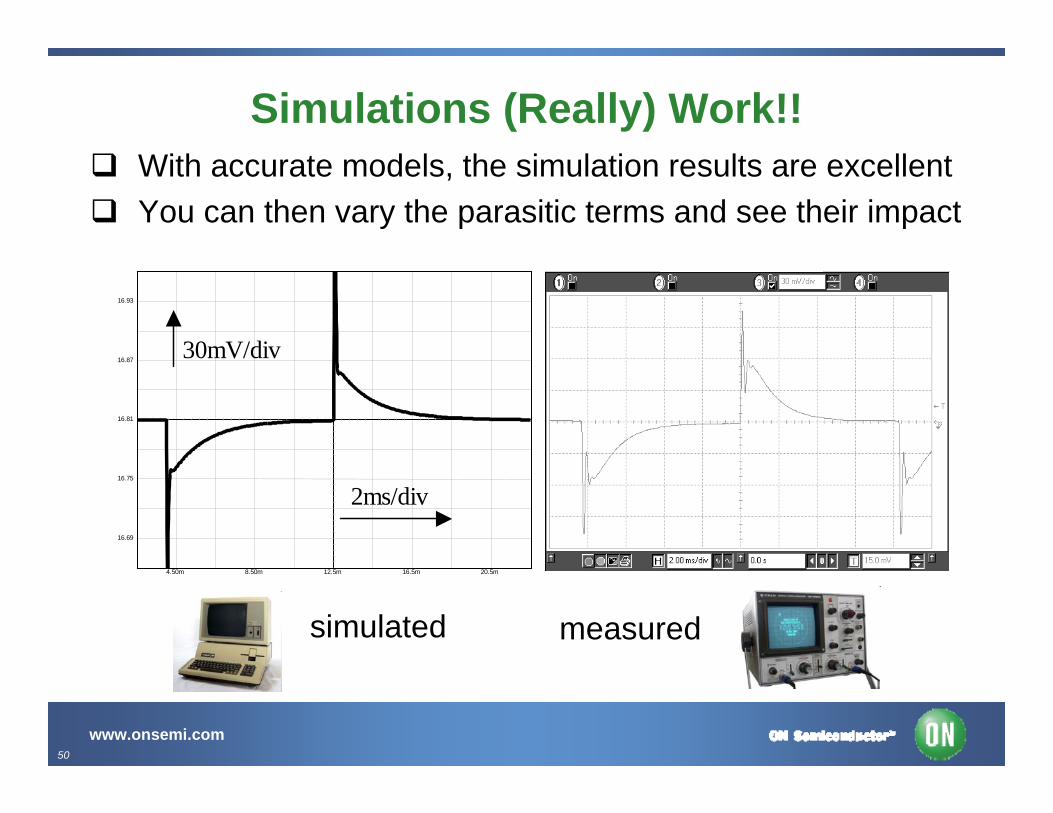
www.onsemi.com50
Simulations (Really) Work!!
4.50m 8.50m 12.5m 16.5m 20.5m
16.69
16.75
16.81
16.87
16.93
30mV/div
2ms/div
With accurate models, the simulation results are excellent You can then vary the parasitic terms and see their impact
simulated measured

www.onsemi.com51
AgendaWhy simulating power supplies?Average modeling techniquesThe PWM switch concept, CCMThe PWM switch concept, DCMThe voltage-mode model at workCurrent-mode modelingThe current-mode model at workPower factor correctionSwitching modelsEMI filteringConclusion

www.onsemi.com52
EMI Filtering on a DC-DC
7
5
10
8
2 4
Vdrv
Verr
Vsense VIL
Vrect
Vout
ID_FW
3
ICoil
9
R3285
C311n
C21.3nF
13R2120k
CMP
FBOUT
GNDIMAX
X1PWMVMPERIOD = 10uDUTYMAX = 0.9REF = 2.5IMAX = 5DUTYMIN = 0.01VOL = 100MVOH = 2.5DUTYMIN = 0.01
6X2PSW1RON = 0.1
C13.3nF
D1mbr845
Rupper38k
Rlimit10m
1
R150m
L1180uH
14Cout1000uFIC = 11
Resr69m
C30470p
R301k
B1VoltageI(Rlimit)
Rlower10k
Δ
Vswitch
Iin
36
V1
Vin30
vin
Rload3
Need tolimit the
ac current< 15 mA peak
DC-DC are highly EMI polluting systemsA filter has to be installed to avoid noise in the source

www.onsemi.com53
EMI Filtering on a DC-DC
3.922m 3.939m 3.956m 3.974m 3.991mtime in seconds
-4.00
-2.00
0
2.00
4.00
iin in
am
pere
sP
lot1
1
105k 315k 525k 735k 945kfrequency in hertz
10u
100u
1m
10m
100m
1
10
mag
(fft(t
emp)
) in
am
pere
sPl
ot1_
f
2
FFT results
Input current signature
Ipeak = 2.45A
Iavg = 1.7 AIrms = 2.7 A
3.922m 3.939m 3.956m 3.974m 3.991mtime in seconds
-4.00
-2.00
0
2.00
4.00
iin in
am
pere
sP
lot1
1
105k 315k 525k 735k 945kfrequency in hertz
10u
100u
1m
10m
100m
1
10
mag
(fft(t
emp)
) in
am
pere
sPl
ot1_
f
2
FFT results
Input current signature
Ipeak = 2.45A
Iavg = 1.7 AIrms = 2.7 A
15 62.45filter
mA m< <
Iripple < 15 mAattenuation
0 0.006 7.7swf F kHz< × <
Position the cutofffrequency of the LC filter
Use SPICE to extract the current signatureRun Fourier analysis to look at the spectrum

www.onsemi.com54
EMI Filtering on a DC-DC
Vin
L Rlf
C Rload VoutSwitchModeConverter
2 20
1 5.24
C µFf Lπ
= =
L = 100 µH
Checkimpedance
peaking
220 1
max1 0
1outFILTERZ RZR Z
⎛ ⎞= + ⎜ ⎟
⎝ ⎠
7.7 kHz
A LC configuration offers the best efficiencyAs any LC network, it is subject to resonances

www.onsemi.com55
EMI Filtering on a DC-DC
10m 100m 1 10 100 1k 10k 100kfrequency in hertz
-30.0
-10.0
10.0
30.0
50.0
pp
1
7
Zout
No dampingZout = 57.5 dBΩ
ZinSMPS
18 dBΩ
Problem!
10m 100m 1 10 100 1k 10k 100kfrequency in hertz
-30.0
-10.0
10.0
30.0
50.0
pp
1
7
Zout
No dampingZout = 57.5 dBΩ
ZinSMPS
18 dBΩ
Problem!
Need todamp this!
The incremental input resistance of a DC-DC in negativeA LC filter loaded by a negative resistance can oscillate!
Powersupply inputimpedance

www.onsemi.com56
EMI Filtering on a DC-DC
10 100 1k 10k 100kfrequency in hertz
-40.0
-20.0
0
20.0
40.0
vdbo
ut2,
vdb
out2
#1 in
db(
volts
)
-180
-90.0
0
90.0
180
ph_v
out2
#1,
ph_v
out2
in d
egre
esP
lot1
2
3
41
phase
gainWith filter
With filter
Without filter
Without filter
10 100 1k 10k 100kfrequency in hertz
-40.0
-20.0
0
20.0
40.0
vdbo
ut2,
vdb
out2
#1 in
db(
volts
)
-180
-90.0
0
90.0
180
ph_v
out2
#1,
ph_v
out2
in d
egre
esP
lot1
2
3
41
phase
gainWith filter
With filter
Without filter
Without filter
Not stable!
If the resonance is too peaky, problems can arise
|T(s)|
argT(s)

www.onsemi.com57
EMI Filtering on a DC-DC
Vin
L Rlf
C Rload VoutSwitchModeConverter
11 2
0
11 2 1
0 0
2damp inSMPS
inSMPSinSMPS
RL CR RR Z Z RZ CR L CR R
ω
ω ω
+ −= −
− + + −
A resistor is damping the LC filter by creating lossesA dc-block capacitor is installed to limit dissipation
www.onsemi.com58
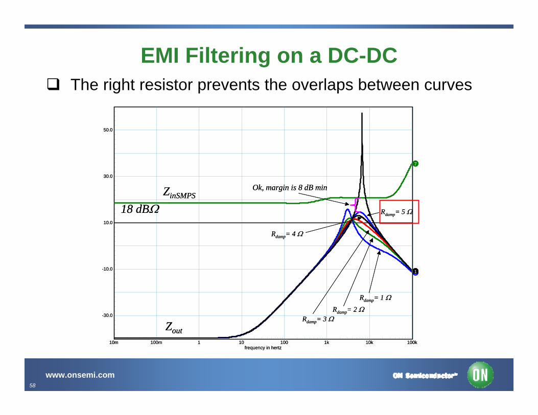
EMI Filtering on a DC-DC
10m 100m 1 10 100 1k 10k 100kfrequency in hertz
-30.0
-10.0
10.0
30.0
50.0
7
654321
Zout
ZinSMPS
18 dBΩ
Ok, margin is 8 dB min
Rdamp= 1 Ω
Rdamp= 2 ΩRdamp= 3 Ω
Rdamp= 4 Ω
Rdamp= 5 Ω
10m 100m 1 10 100 1k 10k 100kfrequency in hertz
-30.0
-10.0
10.0
30.0
50.0
7
654321
Zout
ZinSMPS
18 dBΩ
Ok, margin is 8 dB min
Rdamp= 1 Ω
Rdamp= 2 ΩRdamp= 3 Ω
Rdamp= 4 Ω
Rdamp= 5 Ω
The right resistor prevents the overlaps between curves

www.onsemi.com59
EMI Filtering on a DC-DC
3.82m 3.86m 3.90m 3.94m 3.98mtime in seconds
1.660
1.670
1.680
1.690
1.700
p
0 1
1
y (pk-pk) = 22.8m amperesbetween 3.91m and 3.92m seconds
A final check shows a noise amplitude under control

www.onsemi.com60
A Book on Power Supply Design
Learn DC-DC converters theoryUnderstand average modelingFeedback and loop controlDesign examples of DC-DC and AC-DCPower Factor CorrectionChapters on flyback and forward convertersSupplied CDROM with working examples
To learn more about power supplies and simulations…
I alreadyhave ideasfor the nextedition!!
886 pages, 8 chapters

www.onsemi.com61
Conclusion
SPICE can be seen as a design companion
It shields us from going through complex equations
Simulation time is short and PC helps to run tests
Use SPICE before going to the bench: NO trial and error!
Once the simulation is stable, build the prototype
Simulations and laboratory debug: the success recipe!

www.onsemi.com62
For More Information
• View the extensive portfolio of power management products from ON Semiconductor at www.onsemi.com
• View reference designs, design notes, and other material supporting the design of highly efficient power supplies at www.onsemi.com/powersupplies