Embed Size (px)
Citation preview

Simulator Acceleration and Inverse Design of FinField-Effect Transistors Using Machine LearningInsoo Kim
Korea UniversitySo Jeong Park
Korea UniversityChangwook Jeong
Samsung ElectronicsMunbo Shim
Samsung ElectronicsDae Sin Kim
Samsung ElectronicsGyu-Tae Kim
Korea UniversityJunhee Seok ( [email protected] )
Korea University
Research Article
Keywords: Simulator Acceleration, Inverse Design, Fin Field-Effect Transistors, Machine Learning,electronic devices, transistors, semiconductor industry
Posted Date: August 11th, 2021
DOI: https://doi.org/10.21203/rs.3.rs-789509/v1
License: This work is licensed under a Creative Commons Attribution 4.0 International License. Read Full License

Simulator Acceleration and Inverse Design of Fin Field-Effect
Transistors using Machine Learning
Insoo Kim1, So Jeong Park1, Changwook Jeong2, Munbo Shim2, Dae Sin Kim2, Gyu-Tae
Kim1, Junhee Seok1,*
1School of Electrical Engineering, Korea University, Seoul, Korea
2Computational Science and Engineering Team,
Data and Information Technology Center, Samsung Electronics, Samsungjeonja-ro,
Hwaseong-si, Gyeonggi-do 18448, South Korea
* Correspondence should be addressed to [email protected]

Abstract
The simulation and design of electronic devices such as transistors is vital for the
semiconductor industry. Conventionally, a device is intuitively designed and simulated using
model equations, which is a time-consuming and expensive process. However, recent
machine learning approaches provide an unprecedented opportunity to improve these tasks by
training the underlying relationships between the device design and the specifications derived
from the extensively accumulated simulation data. This study implements various machine
learning approaches for the simulation acceleration and inverse-design problems of fin field-
effect transistors. In comparison to traditional simulators, the proposed neural network model
demonstrated almost equivalent results (R2 = 0.99) and was more than 122,000 times faster in
simulation. Moreover, the proposed inverse-design model successfully generated design
parameters that satisfied the desired target specifications with high accuracies (R2 = 0.96).
Overall, the results demonstrated that the proposed machine learning models aided in
achieving efficient solutions for the simulation and design problems pertaining to electronic
devices. Thus, the proposed approach can be further extended to more complex devices and
other vital processes in the semiconductor industry.

Introduction
Since the development of metal-oxide-semiconductor field-effect transistor
(MOSFET) device, it took us only 70 years to carry a computer in our pockets that is a billion
times faster than the first computer. However, the compression of the traditional MOSFET to
the nanoscale has induced certain physical limitations such as the short-channel effects.
Consequently, new MOSFET devices such as a fin field-effect transistor (FinFET) and a gate-
all-around field-effect-transistor device have been proposed to surpass these limitations1,2.
The recently suggested MOSFET devices pose new challenges related to their
designs. In particular, the establishment of an appropriate design that meets the desired
specifications is one of the major design problems regarding these new MOSFET devices,
referred to as the inverse-design problem. Thus, a potential solution involves testing
numerous devices with various designs until the desired device is determined. However, such
a solution is not feasible because the manufacturing of numerous MOSFET devices with
distinct designs for reviewing their specifications is a time-consuming and expensive
endeavor. Therefore, simulation-based estimation of specifications can be considered as a
reasonable approach to review the design of a FinFET device3. Nevertheless, the
conventional concept of obtaining solutions from differential equations describing physical
laws is still a complex task and requires the prior knowledge of an expert. In addition, this
approach can predict only the specifications of the devices from the design, typically the
device parameter. Thus, these facts imply that the one-way approach is an unsuitable solution
for the inverse-design problem.
Recently, the explosive growth of machine learning models such as deep neural
networks has provided improved solutions for several complex problems. For instance, deep-
generative models have been recently implemented to solve complex inverse-design
problems in various fields such as nanophotonics and molecular designs4-8. Moreover, recent
studies reported that the deep neural networks can provide an efficient solution for solving
Maxwell equations, which are partial differential equations calculating the electromagnetic
values of a given space9-11.
Although the implementation of machine learning and deep learning models have
yielded significant advances in several related fields, the direct application of such
approaches in the semiconductor design problems has recently been initiated12. In this study,
we propose a guideline to implement machine learning models in semiconductor device
simulation and design problems. In particular, we applied log-reciprocal normalization for
data preprocessing, implemented neural network models with a combined loss function for
simulation acceleration, and introduced model-based device design. The experimental results
aimed to determine the capability of the proposed machine learning approach in solving both
the simulation acceleration and inverse-design problems with adequate accuracy.
2. Result and Discussions
2.1 Data preprocessing with log reciprocal normalization
The input and output samples used for training and testing the proposed methods
were generated using a FinFET simulator constructed with FlexPDE13. The FinFET simulator
was developed to calculate the device parameter of a given FinFET design. The four design
parameters of the FinFET device include the channel top width (𝑊𝑇), channel bottom width
(𝑊𝐵), channel thickness (𝑇𝑆𝑖 ), and backgate voltage (𝑉𝐵𝑔), which were used as input
parameters for the FinFET simulator. In particular, the three device parameters of the FinFET
device—the drain current (𝐼𝐷), effective mobility (𝜇), and electron charge density (𝑄𝑁)—
were regarded as the output values calculated using the simulator. Additionally, three device
parameters —subthreshold swing (𝑆𝑆𝑤), threshold voltage (𝑉𝑇ℎ), and mobility degradation
(𝜇𝐷𝑒𝑔) of the FinFET device were calculated from the device parameters (𝐼𝐷, 𝜇) in order to be
used as the input values and the evaluation methods of the proposed models. In the paper, the
three device parameters directly calculated through the simulators (𝐼𝐷, 𝜇, 𝑄𝑁) were referred
as primary properties and three device parameters calculated from the primary properties with
the implicit functions were referred as secondary properties. These design and properties are
summarized in Table S1. As the original values of the design and primary properties were not
in appropriate ranges for training, these values were normalized prior to the training
procedure. In particular, the four design parameters and three primary properties were
normalized in between 0 and 1 with the min–max normalization and the log-reciprocal
normalization, respectively. Moreover, the log-reciprocal normalization used in this study can
be expressed as follows, where the maximum value was considered across all the training
samples.

𝐼𝐷,𝑛𝑜𝑟𝑚 = max (log 𝐼𝐷)log 𝐼𝐷 µ𝑛𝑜𝑟𝑚 = μmax (𝜇)
𝑄𝑁,𝑛𝑜𝑟𝑚 = max (log 𝑄𝑁)log 𝑄𝑁 The log-reciprocal normalization was proposed for the semiconductor design
problems owing to the special characteristic of the primary properties. In particular, the
values of 𝐼𝐷 and 𝑄𝑁 at the subthreshold voltages, which are typically under 0 V, were
relatively small as compared to those around and over the threshold voltages. The
conventional log normalization converts the 𝐼𝐷 and 𝑄𝑁 values at subthreshold voltages to
relatively large negative values compared to the values at threshold voltages and over. Owing
to this unbalanced value distribution, the conventional log normalization biases the model to
fit the subthreshold voltages, which consequently distorts the transfer characteristics (𝐼𝐷/𝑉𝐺)
curve. In contrast, the log-reciprocal normalization tends to reduce the extreme values of 𝐼𝐷
and 𝑄𝑁, and subsequently, prevents the value distribution from having a long tail. Moreover,
it preserves the desirable shape and tendency of the 𝐼𝐷/𝑉𝐺 curve, which are heavily related to
the significant specification of the semiconductor device and is a common topic of research.
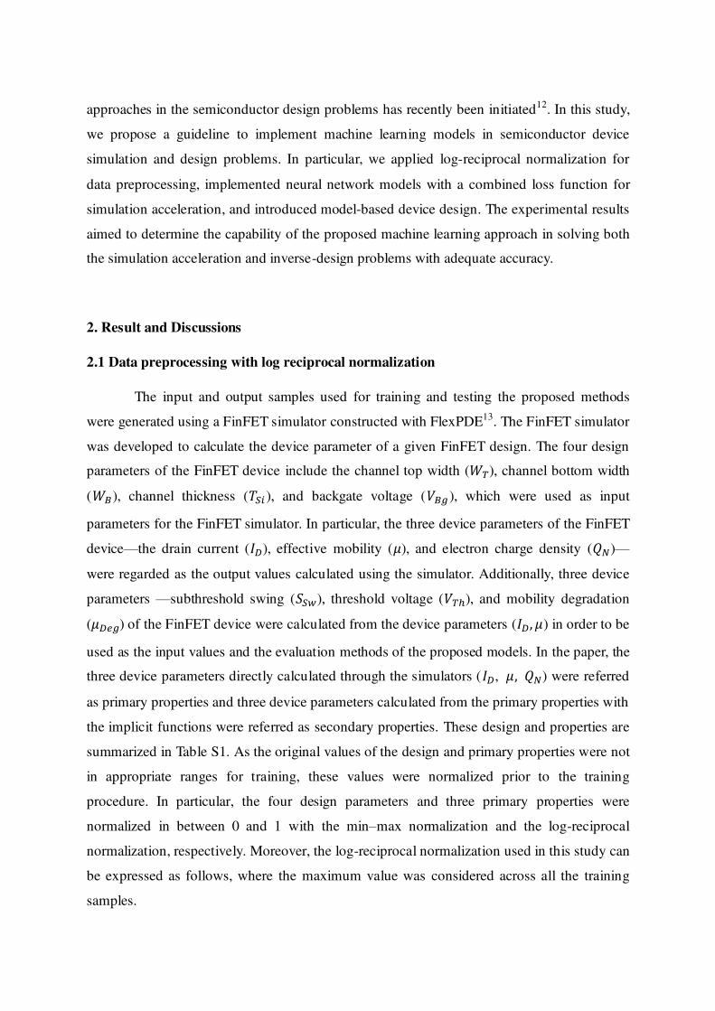
The distributions of 𝐼𝐷 at various voltages are presented in Figure 1, which depicts the log-
reciprocal normalization converting the data distribution as more Gaussian-like.
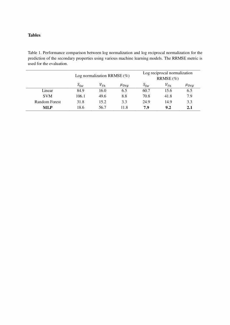
Consequently, the log-reciprocal normalization delivered superior performance in
predicting the secondary properties that are essential device specifications. The models were
trained with 3,500 training samples and the relative root–mean–square error (RRMSE) was
measured over 500 validation samples. As compared to the conventional log normalization,
the log-reciprocal normalization displayed improved or at least equivalent prediction errors
for all the models. On average, the log-reciprocal normalization method reduced the RRMSE
by 28.2%. In particular, the multilayer perceptron (MLP) model in coordination with the
proposed log normalization method delivered performance improvements of 58.6%, 83.3%,
and 82.2% as compared to the MLP model with the log normalization, respectively. Moreover,
the RRMSEs of the MLP model were respectively 68.2%, 38.3%, and 63.6% lesser than
those reported by the best machine learning models using log-reciprocal normalization. The

performances of the proposed log-reciprocal normalization and the conventional log
normalization are comparatively presented in Table 1 for cases involving various baseline
machine learning models. The results implied that the log-reciprocal normalization can
improve the data presentation for the semiconductor simulation and design problems.
2.2 Simulator acceleration model
The proposed simulator acceleration model was developed to accelerate the existing
FinFET channel simulator while achieving prediction results that are comparable to those
obtained using traditional simulators. In general, the traditional simulators can predict the
device properties by numerically solving the differential equations that describes the
electromagnetic relationships. In contrast, the acceleration models aim to approximate the
traditional simulators by finding an implicit function between the properties and design
parameters based on the accumulated simulation data. Herein, the proposed acceleration
model was designed to predict the three primary properties of the FinFET device (𝐼𝐷, 𝜇, 𝑄𝑁)
based on the four design parameters (𝑊𝑇, 𝑊𝐵 𝑇𝑆𝑖, 𝑉𝐵𝑔).
The proposed simulation accelerator aimed to predict both the primary and secondary
properties according to the device design. As a traditional simulator can generally predict
only the primary properties, the secondary properties are calculated using explicitly defined
equations. Similarly, the machine learning model of the accelerator can be trained to target
only the primary properties, in which case, the loss function can be expressed as follows.
𝐿𝑜𝑠𝑠 = ∑{(𝐼𝐷,𝑛𝑜𝑟𝑚 − 𝐼𝐷,𝑛𝑜𝑟𝑚)2 + (μ𝑛𝑜𝑟𝑚 − �̂�𝑛𝑜𝑟𝑚)2 + (𝑄𝑁,𝑛𝑜𝑟𝑚 − �̂�𝑁,𝑛𝑜𝑟𝑚)2} However, in such an approach, small prediction errors in the primary properties can
induce large distortions in the calculation of the secondary properties. Thus, a combined loss
function considering both the primary and secondary properties was proposed.
𝐿𝑐𝑜𝑚𝑏𝑖𝑛𝑒𝑑 = ∑{(𝐼𝐷,𝑛𝑜𝑟𝑚 − 𝐼𝐷,𝑛𝑜𝑟𝑚)2 + (μ𝑛𝑜𝑟𝑚 − �̂�𝑛𝑜𝑟𝑚)2 + (𝑄𝑁,𝑛𝑜𝑟𝑚 − �̂�𝑁,𝑛𝑜𝑟𝑚)2+ (𝑆𝑆𝑤 − 𝑆𝑆𝑤,𝑙𝑜𝑠𝑠)2 + (𝑉𝑇ℎ − �̂�𝑇ℎ,𝑙𝑜𝑠𝑠)2 + (𝜇𝐷𝑒𝑔 − �̂�𝐷𝑒𝑔,𝑙𝑜𝑠𝑠)2}
Here, the prediction of the primary properties, 𝐼𝐷,𝑛𝑜𝑟𝑚, �̂�𝑛𝑜𝑟𝑚, and �̂�𝑁,𝑛𝑜𝑟𝑚 are the
direct output of the acceleration model and the prediction of the secondary properties, 𝑆𝑆𝑤,

�̂�𝑇ℎ, and �̂�𝐷𝑒𝑔 were estimated from the predicted primary properties using their explicit
relations.
As described in the Methods section, a two-layered MLP model was developed and
trained with 3,500 training samples using the proposed combined loss function. Additionally,
the parameters were tuned with 500 validation samples, and the effectiveness of the proposed
combined loss function was verified by comparing the performance of the proposed model
with that of several machine learning methods trained only using the primary property losses.
Subsequently, the performances were evaluated by comparing the RRMSEs of the 𝑆𝑆𝑤, �̂�𝑇ℎ,
and �̂�𝐷𝑒𝑔 observed in the prediction results. Overall, the performances were measured over
500 validation and 1,000 test samples.
The proposed simulator acceleration model with the combined loss function
displayed high accuracy in predicting both the primary and secondary properties. In the 1,000
test samples, the RRMSEs of the primary properties 𝐼𝐷,𝑛𝑜𝑟𝑚, �̂�𝑛𝑜𝑟𝑚, and �̂�𝑁,𝑛𝑜𝑟𝑚 were
0.0028%, 0.0020%, and 0.0022%, and those of the secondary properties 𝑆𝑆𝑤, �̂�𝑇ℎ, and �̂�𝐷𝑒𝑔
were 5.7%, 3.6%, and 1.3%, respectively. These improvements are noteworthy in comparison
to the baseline models. Moreover, the RRMSEs of the proposed combined-loss MLP in the
1,000 test samples were 30.5%, 69.7%, and 48.0% lesser than those of the best alternative
methods, respectively. Additionally, all the R2 scores of the secondary properties determined
using the combined loss MLP model were beyond 0.99. The results are comparatively
presented in Table 2. Furthermore, the scatter plots between the predicted and real secondary
property values are presented in Figure 2, which demonstrates good agreement of the
prediction results. Thus, the results implied that the combined-loss MLP model can
successfully learn the tendency of the primary properties and preserve the shape of the
primary property curves as compared to the alternative baseline models.
More importantly, the proposed simulator acceleration model successfully reduced
the computation time compared to the traditional FinFET simulator. The average
computational time of a FinFET simulator is 70 s/sample and a total of 90 h is required to
simulate 5,000 samples. Comparatively, the proposed simulator acceleration model required
only 2.52 s to calculate 5,000 samples, which is approximately 122,000 times faster than the
traditional FinFET simulator.

2.3 Inverse-Design model
In addition to the development of the specialized preprocessing method and loss
function for the semiconductor design problems, we demonstrate the utility of the deep neural
networks for the semiconductor inverse-design problem. The inverse-design model aimed to
directly predict the design of a semiconductor device that holds same specifications with the
desired specifications which are the input of the model. Thus, the proposed inverse-design
model aimed to predict the four design parameters of the FinFET device (𝑊𝑇, 𝑊𝐵 𝑇𝑆𝑖, 𝑉𝐵𝑔)
from the desired secondary properties of the FinFET device (𝑆𝑆𝑤, 𝑉𝑇ℎ, 𝜇𝐷𝑒𝑔).
Similar to the simulator acceleration model, a two-layered MLP model was
developed and trained with 3,500 training samples. In addition, the parameters were tuned
with 500 validation samples, and the performance of the model was evaluated by comparing
the desired specifications used as an input of the model with the actual specifications of the
designed device, which were derived from the traditional FinFET simulator. Subsequently,
the performance was measured over 1,000 random specifications.
Upon evaluating with the actual specifications, the proposed model displayed
adequate performance in design prediction. In particular, the performance of the inverse
design was evaluated based on the error between the target and actual specifications of the
predicted designs as calculated using the FinFET simulator. As depicted in Figure 3, the
target and actual specifications agreed well with each other for the all the three secondary
properties ( 𝑆𝑆𝑤 , 𝑉𝑇ℎ , 𝜇𝐷𝑒𝑔 ). Moreover, the R2 scores of 𝑆𝑆𝑤 , 𝑉𝑇ℎ , and 𝜇𝐷𝑒𝑔 were
measured as 0.96, 0.97, and 0.97, respectively. Although the proposed design prediction
appropriately satisfied the desired specifications, yielding the desired 𝑆𝑆𝑤 is challenging,
especially for low values. This is probably because 𝑆𝑆𝑤 is a kind of gradient that is easily
distorted with small errors. In contrast, the actual 𝑉𝑇ℎ and 𝜇𝐷𝑒𝑔 of 1,000 cases calculated
from the predicted designs were highly similar to the target 𝑉𝑇ℎ and 𝜇𝐷𝑒𝑔. In detail, the
variations in 91% and 99% of 𝑉𝑇ℎ and 𝜇𝐷𝑒𝑔 were within 10% of the target specifications,
whereas those in 82% of 𝑆𝑆𝑤 were under 10%. Upon considering all the three specifications,
73% of cases were determined within the 10% range of the target specifications. The detailed
comparison results of the actual and target specifications in terms of tolerance are presented
in Table 3.
Overall, the predicted design parameters displayed positive correlations with the

original design parameters used in generating the test samples (Figure S1), which implied that
the proposed design prediction followed the general trends. The R2 values of 𝑊𝑇, 𝑊𝐵, 𝑇𝑆𝑖, and 𝑉𝐵𝑔 were 0.47, 0.69, 0.75, and 0.96, respectively. The proposed design prediction
reproduced the original design parameters of 𝑉𝐵𝑔 almost identically, whereas the remaining
three design parameters (𝑊𝑇, 𝑊𝐵, and 𝑇𝑆𝑖) exhibited relatively less correlation. Notably, the
desired specifications were well satisfied, regardless of certain discrepancies in the predicted
and original design parameters. This is largely because the inverse-design problems generally
have multiple solutions, implying that the same specifications can be produced from various
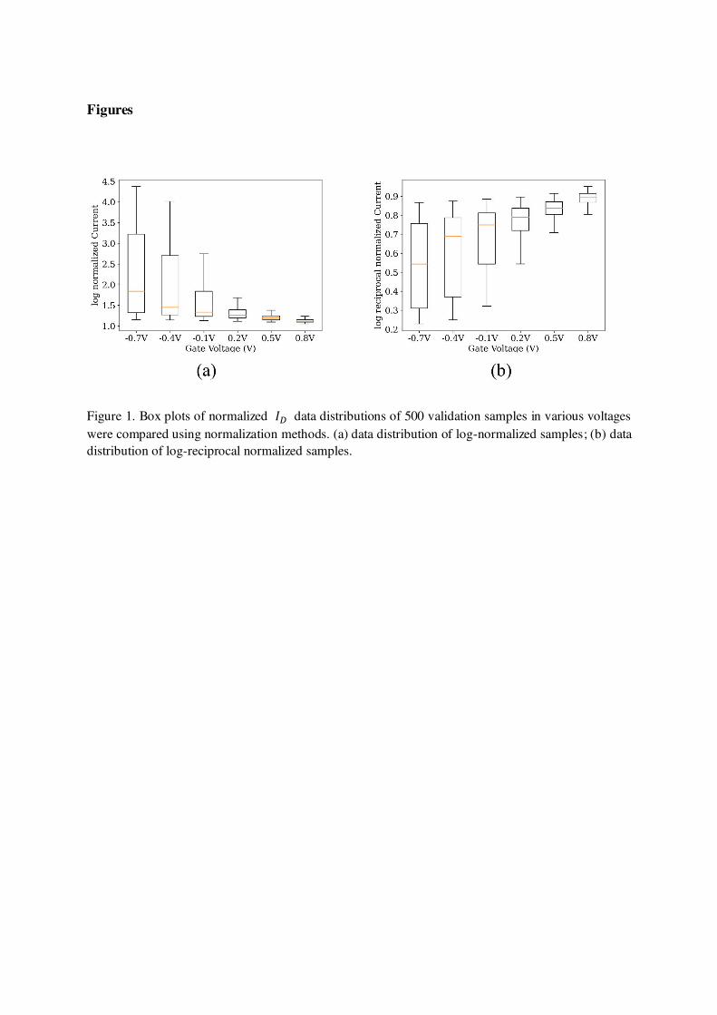
designs. A typical example is presented in Figure 4, which demonstrates the 𝐼𝐷/𝑉𝐺 curve and
the channel design of the two distinct samples. The blue lines in Figure 4 denote the 𝐼𝐷/𝑉𝐺 curves calculated using the FinFET simulator based on the design parameters, and the
channel design of the samples is located above the 𝐼𝐷/𝑉𝐺 curve. Additionally, the orange
lines in Figure 4 express the linear gradients extracted from the amplifying region of the 𝐼𝐷/𝑉𝐺 curve. Moreover, the green dots in Figure 4 denote the threshold voltage (𝑉𝑇ℎ) of the
samples derived from the orange lines. Figure 4a depicts the results of a sample selected from
the test set with relatively low 𝑇𝑆𝑖 as compared to 𝑊𝑇 and 𝑊𝐵. Comparatively, Figure 4b
depicts the results of a sample predicted using the inverse-design model to have the same
specifications as that in Figure 4a. Although the design results presented in Figures 4a and 4b
are remarkably distinct, the shapes of the 𝐼𝐷/𝑉𝐺 curves correlated to the threshold voltage of
the device are similar. Thus, the proposed design prediction truly learned the relationship
between the FinFET design and its specification rather than remembering the training
samples. These results further portray the potential of the proposed method to contribute
toward extending human design scopes.
3. Conclusion
Overall, the results demonstrated that the proposed deep neural network models can
be used to resolve both the simulation acceleration and inverse-design problems for FinFET
devices. In particular, the log-reciprocal normalization in the data preprocessing step
improved the prediction accuracy during simulation by balancing the severely skewed data
distribution. In addition, the proposed combined loss in the simulation acceleration model
enabled the accurate prediction of primary properties as well as the further calculation of

secondary properties. As compared to the traditional simulators, the proposed simulation
acceleration model achieved comparable prediction results (R2 = 0.99) and was more than
120,000 times faster. Moreover, the deep learning model can be applied to directly predict the
design parameters using the desired specifications as a typical inverse-design problem. The
actual design specifications derived by the proposed model corresponded well with the
originally desired specifications. Interestingly, we identified cases with two distinct designs
for the same specifications, which implied that the proposed model actually learns the design-
specification relations, not just remembering the train cases. Overall, 73% of the designed
cases obtained using the proposed model satisfied the desired specification of all the three
secondary properties with a 10% error tolerance, which provides a good starting point for a
human expert to initiate the design process.
Although this study focused on a relatively simple FinFET device, a similar approach
can be applied to more complex devices or a small circuit of several FinFET devices. In
general, the discussed machine learning and deep learning approaches will aid in resolving
several device and circuit-related problems that can be further extended to a general
simulation acceleration and inverse-design problems.
4. Data and Methods
4.1 Data generation
A traditional simulator was constructed to characterize the device parameter of a
given FinFET device design using FlexPDE13. The general 3D schematic and 2D cross-
section of a FinFET device are presented in Figure 5, wherein Figure 5a displays the cross-
section of the gate component of the gray fin channel. In addition, the blue, green, and gray
regions in Figure 5b correspond to the oxide, silicon, and oxide box of the channel,
respectively. The traditional simulator solved the Maxwell equations using the boundary
conditions derived from a given design to characterize the device parameter. The detailed
equation derived from the Gauss’s Law is expressed as follows. ∇ ° (𝜀∇𝑉𝐺) = 𝑄𝑇𝑜𝑡𝑎𝑙 The above equation denotes that the total charge in a given region (𝑄𝑇𝑜𝑡𝑎𝑙) is equal to the
divergence (∇ °) of electromagnetic permittivity (𝜀) multiplied with the gradient of gate

voltage (∇𝑉𝐺). In particular, the FlexPDE13 was used to numerically solve the derived partial
differential equations. The detailed conditions of this simulator are listed in Table S2.
As depicted in Figure 5b, a FinFET structure is mainly specified according to the
four design parameters, which include the top and bottom width of the FinFET channel (𝑊𝑇, 𝑊𝐵), the channel thickness (𝑇𝑆𝑖), and the box gate voltage (𝑉𝐵𝑔) imposed on the silicon box.
In addition, the 𝑊𝑇 , 𝑊𝐵, and 𝑇𝑆𝑖 determine the silicon/oxide border length, which is
considered as an effective channel length that significantly influences the device parameter of
a FinFET device. Moreover, the 𝑉𝐵𝑔 imposed on the box under the silicon channel
influenced the overall conductivity across all voltages. Thus, the experiments were focused
on these four parameters as these parameters are significantly correlated with the device
parameter of the semiconductor device and can be conveniently controlled during the
manufacturing process.
Based on the design specified by the four parameters, the primary device parameter
were evaluated according to the gate voltage (𝑉𝐺) variations by solving the differential
equations using the traditional simulator. In particular, the variations in the drain current flow
(𝐼𝐷), effective mobility (𝜇), and electron charge density (𝑄𝑁) with respect to the varying gate
voltage (𝑉𝐺) were calculated using the following equations. 𝐼𝐷 = 𝜎𝑉𝐷 𝜇 = 𝜎𝑄𝑛𝐿
𝑄𝑛 = 𝑞 ∫ 𝑛𝑖𝑒𝑉𝐺𝑘𝑇 𝜎 = ∮ 𝑚𝑞𝑛𝑖𝐿
The 𝐼𝐷, 𝜇, and 𝑄𝑁 values of the device were calculated using the simulator at 50 distinct 𝑉𝐺 values. The range of 𝑉𝐺 was set from –1 to 1.45 V with an interval of 0.05 V per
observation.
Moreover, the three secondary properties of a FinFET device were derived directly
from the primary properties, which are essential for the actual utilization of a semiconductor

device14. In particular, the subthreshold swing (𝑆𝑆𝑤), threshold voltage (𝑉𝑇ℎ), and mobility
degradation (𝜇𝐷𝑒𝑔) were derived as the secondary properties of the FinFET device, which
were characterized by the following equations.
𝑆𝑆𝑤 = 𝑚𝑖𝑛 { 𝑑𝑑𝑉𝐺 log 𝐼𝐷}
𝑉𝑇ℎ = 𝐼𝑑,𝑉𝑎 − 𝑑𝐼𝑑,𝑉𝑎𝑑𝑉𝐺 𝑉𝑎𝑑𝐼𝑑,𝑉𝑎𝑑𝑉𝐺
𝜇𝐷𝑒𝑔 = µ1.0µ 𝑚𝑎𝑥
A subthreshold swing corresponds to the minimum value of the reciprocal of a gradient of the
log 𝐼𝐷 in terms of 𝑉𝐺. A threshold voltage represents the turn-on voltage of a semiconductor.
The 𝑉𝑎 denotes the gate voltages with the 𝐼𝑑 /𝑉𝑔 graph present in the linear region, and the 𝐼𝑑,𝑉𝑎 denotes the value of drain current at the gate voltage 𝑉𝑎. Moreover, the mobility
degradation represents a ratio between the effective mobility value at a certain voltage and
the maximum effective mobility value. In particular, 𝜇1.0 denotes the effective mobility
value at a gate voltage that is 1 V higher than the threshold voltage of the given
semiconductor, and 𝜇𝑚𝑎𝑥 represents the maximum effective mobility value of a given
semiconductor.
Subsequently, the trapezoid-shaped channel FinFET device samples were generated
by modifying the four design parameters (𝑊𝑇, 𝑊𝐵, 𝑇𝑆𝑖, 𝑉𝐵𝑔) using the traditional simulator.
The ranges of these design parameters were defined in physically reasonable regions that can
be applied in actual manufacturing processes. In particular, the bottom width of the sample
was randomly selected within 10–250 nm, whereas the top width of the sample was randomly
selected in between 1 nm and the bottom width. Additionally, the silicon thickness of the
sample was randomly selected between 10 and 50 nm. Lastly, the box gate voltage of the
sample was randomly selected between 0 and 40 V.
A total 5,000 samples were generated using the traditional simulator, and among
these 5,000 samples, 3,500 samples were randomly selected as the training samples, 500
samples were randomly selected as the validation samples, and 1,000 samples are randomly
selected as the test samples. The RRMSE was calculated using the following equation and

used as an evaluation metric of the proposed models in the validation and test stages.
RRMSE (%) = √1𝑛 ∑ (𝑦𝑖𝑟𝑒𝑎𝑙− 𝑦𝑖𝑝𝑟𝑒𝑑𝑖𝑐𝑡)2𝑛𝑖−11𝑛 ∑ 𝑦𝑖𝑟𝑒𝑎𝑙𝑛𝑖=1 × 100
4.2 Model Training
The simulator acceleration model was constructed based on the training samples
generated from the traditional simulator to predict the three primary device parameter (𝐼𝐷, 𝜇, 𝑄𝑁) of the FinFET device using the four design parameters (𝑊𝑇, 𝑊𝐵 𝑇𝑆𝑖, 𝑉𝐵𝑔). Similar to
the traditional simulator, the proposed acceleration model predicted a total of 150 distinct
values of the (𝐼𝐷, 𝜇, 𝑄𝑁) ranging from –1 to 1.45 V in 0.05 V interval of 𝑉𝐺. The proposed
simulator acceleration model is an MLP model integrated with a specialized combined loss
function, as discussed earlier. In addition, the proposed model comprises two hidden layers—
each containing 128 nodes with a rectified linear unit (RELU) operating as an activation
function for the hidden layers and a sigmoid acting as an activation function for the output
layer. During the training procedure, the proposed model was trained for 1,000 epochs with a
batch size of 256. Moreover, an adaptive moment estimation (ADAM) optimizer was
implemented with an initial learning rate of 0.01 with 0.99 decay for every 75 steps to train
the model. Furthermore, the proposed model was trained with a NVDIA RTX 2080 SUPER
GPU and an INTEL 4-core CPU i7-7700k.
An MLP structure was proposed for the inverse-design model as well. The inverse-
design model was developed to predict the four design parameters (𝑊𝑇, 𝑊𝐵 𝑇𝑆𝑖, 𝑉𝐵𝑔) of the
FinFET device by utilizing the target specifications, i.e., the three secondary properties (𝑆𝑆𝑤, 𝑉𝑇ℎ, 𝜇𝐷𝑒𝑔). In particular, the MLP model of the inverse-design problem comprises two
hidden layers—the first layer with 256 nodes and the second layer with 32 nodes. Moreover,
the RELU activation was used for all the hidden layers, and the sigmoid function was used as
an activation function for the output layer. During the training procedure, the proposed model
was trained with a batch size of 32 for 300 epochs, and an ADAM optimizer was
implemented as an optimizer to train the model at a learning rate of 0.003. The proposed
inverse-design model was trained with a NVDIA RTX 2080 SUPER GPU and an INTEL 4-

core CPU i7-7700k.

References
1 Hisamoto, D. et al. FinFET-a self-aligned double-gate MOSFET scalable to 20 nm. IEEE
transactions on electron devices 47, 2320-2325 (2000).
2 Nagy, D. et al. FinFET versus gate-all-around nanowire FET: Performance, scaling, and
variability. IEEE Journal of the Electron Devices Society 6, 332-340 (2018).
3 Pei, G., Kedzierski, J., Oldiges, P., Ieong, M. & Kan, E.-C. FinFET design considerations based
on 3-D simulation and analytical modeling. IEEE Transactions on Electron Devices 49,
1411-1419 (2002).
4 Molesky, S. et al. Inverse design in nanophotonics. Nature Photonics 12, 659-670 (2018).
5 Sanchez-Lengeling, B. & Aspuru-Guzik, A. Inverse molecular design using machine
learning: Generative models for matter engineering. Science 361, 360-365 (2018).
6 Peurifoy, J. et al. Nanophotonic particle simulation and inverse design using artificial
neural networks. 4, eaar4206 (2018).
7 Sanchez-Lengeling, B., Outeiral, C., Guimaraes, G. L. & Aspuru-Guzik, A. Optimizing
distributions over molecular space. An objective-reinforced generative adversarial network
for inverse-design chemistry (ORGANIC). (2017).
8 Ma, W., Cheng, F., Xu, Y., Wen, Q. & Liu, Y. J. A. M. Probabilistic Representation and Inverse
Design of Metamaterials Based on a Deep Generative Model with Semi‐Supervised
Learning Strategy. 31, 1901111 (2019).
9 Kim, W. & Seok, J. Simulation acceleration for transmittance of electromagnetic waves in
2D slit arrays using deep learning. Scientific reports 10, 1-8 (2020).
10 Qi, S. et al. 2D Electromagnetic Solver Based on Deep Learning Technique. IEEE Journal on
Multiscale Multiphysics Computational Techniques (2020).
11 Zhou, Y. et al. An Improved Deep Learning Scheme for Solving 2D and 3D Inverse
Scattering Problems. IEEE Transactions on Antennas (2020).
12 Mirhoseini, A. et al. Chip placement with deep reinforcement learning. arXiv preprint
arXiv:.10746 (2020).
13 FlexPDE. [online] Available: www.pdesolutions.com.
14 Maduagwu, U. A. & Srivastava, V. M. Analytical performance of the threshold voltage and
subthreshold swing of CSDG MOSFET. Journal of Low Power Electronics Applications 9, 10
(2019).

Acknowledgement
This work was supported by Samsung Electronics Co., Ltd (IO201214-08149-01) as well as a
grant from the National Research Foundation of Korea (NRF-2019R1A2C1084778).
Author contributions
All authors conceived the project and design. I.K, S.P., G.T.K, and J.S designed the study. I.K.
and S.P. performed the research. I.K and J.S. drafted the manuscript. S.P., C.J., M.S, D.S.K,
and G.T.K critically reviewed the manuscript. J.S supervised the research. All authors have
read and approved the final manuscript.
Conflict of Interests
We declare no conflict of interests.
Figures
Figure 1. Box plots of normalized 𝐼𝐷 data distributions of 500 validation samples in various voltages
were compared using normalization methods. (a) data distribution of log-normalized samples; (b) data
distribution of log-reciprocal normalized samples.

Figure 2. Scatter plots of predicted and true secondary property: (a) 𝑆𝑆𝑤 , (b) 𝑉𝑇ℎ, and (c) 𝜇𝐷𝑒𝑔 of
1,000 test samples evaluated using primary properties predicted with proposed simulator acceleration
model.

Figure 3. Scatter plots of desired target and actual specifications of secondary property: (a) 𝑆𝑆𝑤 , (b) 𝑉𝑇ℎ, and (c) 𝜇𝐷𝑒𝑔.
Figure 4. The 𝐼𝐷/𝑉𝐺 graphs of an exemplary case of inverse-design problem. (a) 𝐼𝐷/𝑉𝐺curve of test
sample with target specification; (b) 𝐼𝐷/𝑉𝐺 curve of predicted design evaluated using inverse-design
model.

Figure 5. (a) 3D outline schematic of FinFET device; (b) 2D cross-sectional schematic of channel of
FinFET device channel. Green, blue, light gray, and dark gray regions represent the gate, silicon oxide,
silicon channel, and oxide box of the device, respectively.
Tables
Table 1. Performance comparison between log normalization and log reciprocal normalization for the
prediction of the secondary properties using various machine learning models. The RRMSE metric is
used for the evaluation.
Log normalization RRMSE (%)
Log reciprocal normalization
RRMSE (%) 𝑆𝑆𝑤 𝑉𝑇ℎ 𝜇𝐷𝑒𝑔 𝑆𝑆𝑤 𝑉𝑇ℎ 𝜇𝐷𝑒𝑔
Linear 84.9 16.0 6.5 60.7 15.6 6.5
SVM 106.1 49.6 8.8 70.8 41.8 7.9
Random Forest 31.8 15.2 3.3 24.9 14.9 3.3
MLP 18.6 56.7 11.8 7.9 9.2 2.1

Table 2. Performance comparison of the proposed combined loss MLP model with other machine
learning models for secondary property predictions. The RRMSE metric is used for the evaluation.
Validation set RRMSE (%) Test set RRMSE (%) 𝑆𝑆𝑤 𝑉𝑇ℎ 𝜇𝐷𝑒𝑔 𝑆𝑆𝑤 𝑉𝑇ℎ 𝜇𝐷𝑒𝑔
Linear 60.5 14.2 5.9 68.9 14.7 6.3
SVM 74.5 41.5 7.8 80.0 39.9 8.0
Random Forest 32.9 23.7 4.9 37.2 24.2 5.2
MLP 8.8 11.7 2.4 8.2 11.9 2.5
Combined Loss MLP 5.3 6.7 1.8 5.7 3.6 1.3

Table 3. Percentages of the design cases that meet the target specifications within specific relative
tolerance. The tolerance is the allowed maximum ratio of the difference between the actual and target
values over the target value.
Tolerance 𝑆𝑆𝑤 𝑉𝑇ℎ 𝜇𝐷𝑒𝑔 All
< 20% 81.9% 98.7% 99.9% 80.9%
< 10% 78.2% 91.0% 98.9% 72.5%
< 5% 72.9% 66.6% 93.1% 51.1%

Supplementary Files
This is a list of supplementary �les associated with this preprint. Click to download.
Supplementary.docx


![Acceleration bundles on Banach and Fréchet manifolds...Inverse limit Hilbert manifolds and inverse limit Hilbert groups, introduced by Omori [16, 17], provide an appropriate setting](https://img.pdfslide.net/doc/110x75/6102db5fefbbdc2604459a2c/acceleration-bundles-on-banach-and-frchet-manifolds-inverse-limit-hilbert.jpg)