Embed Size (px)
Citation preview
����������������
Single-Atom Transistors:
Atomic-scale Electronic Devices in
Experiment and Simulation
Fang-Qing Xie1,4
, Robert Maul2,3,4
,
Wolfgang Wenzel4,5
, Gerd Sch�n3,4,5
,
Christian Obermair1,4
and Thomas Schimmel1,4,5,*
1Institute of Applied Physics, Karlsruhe Institute of Technology (KIT),Campus South, 76131 Karlsruhe, Germany
2Steinbuch Centre of Computing, Karlsruhe Institute of Technology,Campus North, 76021 Karlsruhe, Germany
3Institut fur Theoretische Festkorperphysik, Karlsruhe Institute of Technology (KIT),Campus South, 76131 Karlsruhe, Germany
4Center for Functional Nanostructures (CFN), Karlsruhe Institute of Technology(KIT), 76131 Karlsruhe, Germany
5Institute of Nanotechnology, Forschungszentrum Karlsruhe, Karlsruhe Institute ofTechnology (KIT), 76021 Karlsruhe, Germany
E-Mail: *[email protected]
Received: 1st September 2010 / Published: 13th June 2011
Abstract
Controlling the electronic conductivity on the quantum level will im-
pact the development of future nanoscale electronic circuits with ultra-
low energy consumption. Here we report about the invention of the
single-atom transistor, a device which allows one to open and close an
electronic circuit by the controlled and reproducible repositioning of
one single atom. The atomic switching process is induced by a voltage
applied to an independent, third ‘‘gate’’ electrode. In addition to the
demonstration of single-atom switches, the controlled and reproducible
operation of multi-atom quantum switches is demonstrated both in
experiment and in atomistic calculation. Atomistic modelling of
structural and conductance properties elucidates bistable electrode
213
http://www.beilstein-institut.de/Bozen2010/Proceedings/Schimmel/Schimmel.pdf
Functional Nanoscience
May 17th – 21st, 2010, Bozen, Italy
reconstruction as the underlying operation mechanism of the devices.
Atomic transistors open intriguing perspectives for the emerging fields
of quantum electronics and logics on the atomic scale.
Introduction
Fascinating physical properties and technological perspectives have motivated investigation
of atomic-scale metallic point contacts in recent years [1 – 10]. The quantum nature of the
electron is directly observable in a size range where the width of the contacts is comparable
to the Fermi wavelength of the electrons, and conductance is quantized in multiples of 2e2/h
for ballistic transport through ideal junctions [2].
In metallic point contacts, which have been fabricated by mechanically controlled deforma-
tion of thin metallic wires [2 – 4] and electrochemical fabrication techniques [1, 5 – 7] the
conductance depends on the chemical valence [2, 3]. Two-terminal conductance-switching
devices based on quantum point contacts were developed both with an STM-like setup [8]
and with electrochemical methods [9].
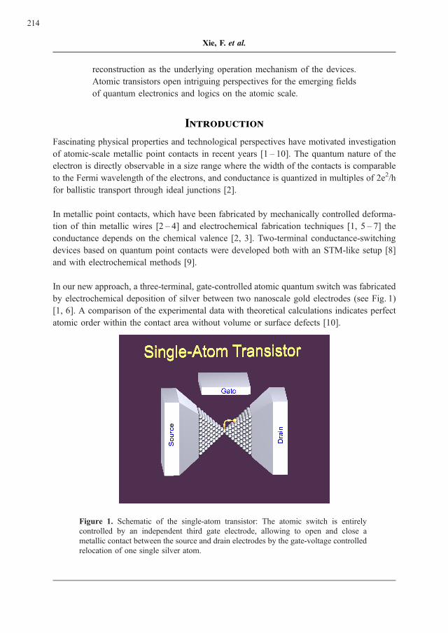
In our new approach, a three-terminal, gate-controlled atomic quantum switch was fabricated
by electrochemical deposition of silver between two nanoscale gold electrodes (see Fig. 1)
[1, 6]. A comparison of the experimental data with theoretical calculations indicates perfect
atomic order within the contact area without volume or surface defects [10].
Figure 1. Schematic of the single-atom transistor: The atomic switch is entirely
controlled by an independent third gate electrode, allowing to open and close a
metallic contact between the source and drain electrodes by the gate-voltage controlled
relocation of one single silver atom.
214
Xie, F. et al.
Switching an Atom
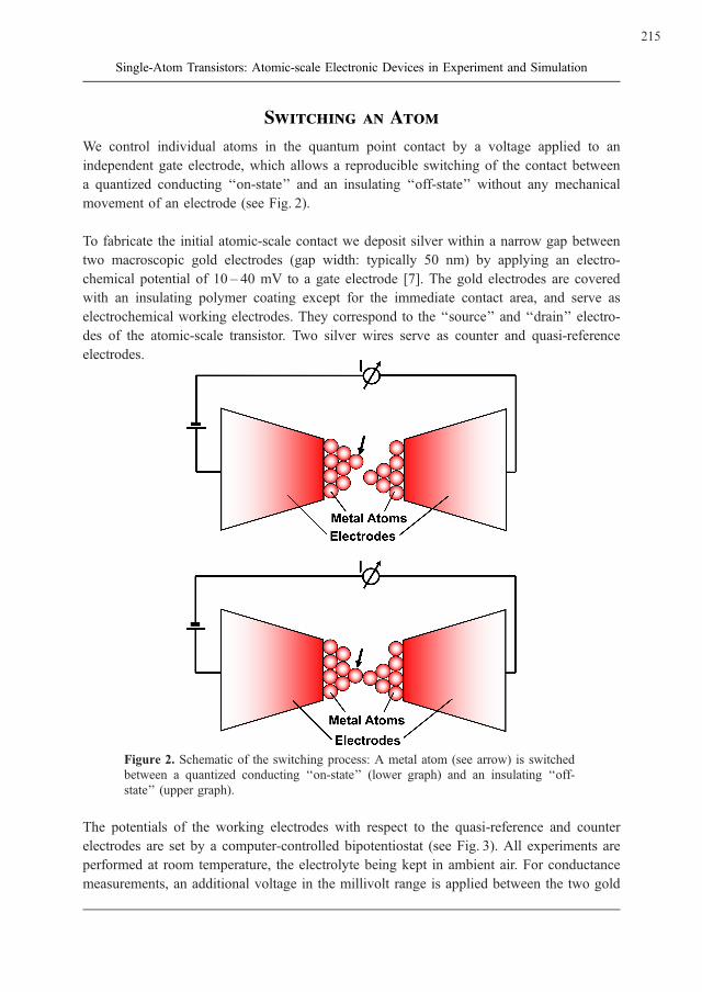
We control individual atoms in the quantum point contact by a voltage applied to an
independent gate electrode, which allows a reproducible switching of the contact between
a quantized conducting ‘‘on-state’’ and an insulating ‘‘off-state’’ without any mechanical
movement of an electrode (see Fig. 2).
To fabricate the initial atomic-scale contact we deposit silver within a narrow gap between
two macroscopic gold electrodes (gap width: typically 50 nm) by applying an electro-
chemical potential of 10 – 40 mV to a gate electrode [7]. The gold electrodes are covered
with an insulating polymer coating except for the immediate contact area, and serve as
electrochemical working electrodes. They correspond to the ‘‘source’’ and ‘‘drain’’ electro-
des of the atomic-scale transistor. Two silver wires serve as counter and quasi-reference
electrodes.
Figure 2. Schematic of the switching process: A metal atom (see arrow) is switched
between a quantized conducting ‘‘on-state’’ (lower graph) and an insulating ‘‘off-
state’’ (upper graph).
The potentials of the working electrodes with respect to the quasi-reference and counter
electrodes are set by a computer-controlled bipotentiostat (see Fig. 3). All experiments are
performed at room temperature, the electrolyte being kept in ambient air. For conductance
measurements, an additional voltage in the millivolt range is applied between the two gold
215
Single-Atom Transistors: Atomic-scale Electronic Devices in Experiment and Simulation
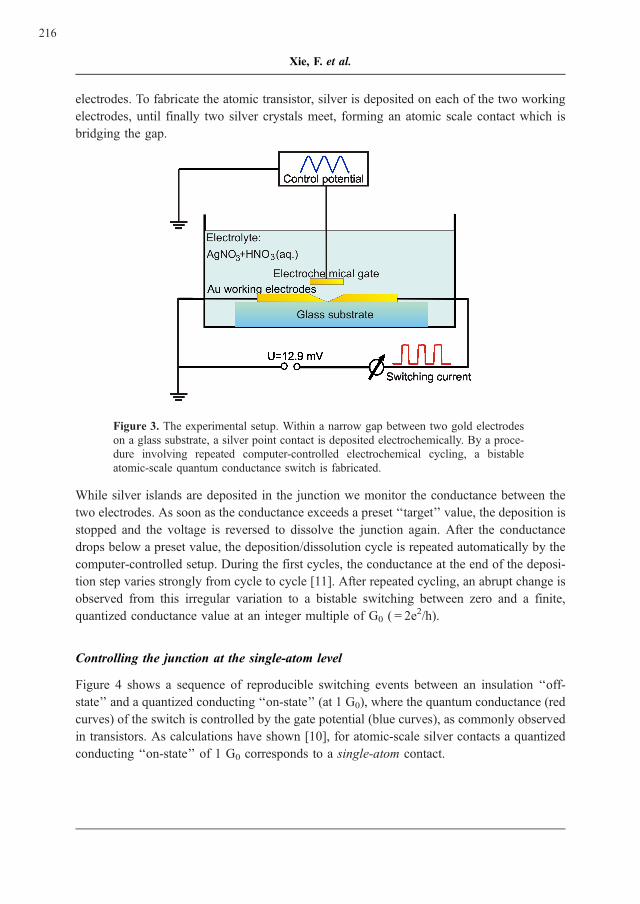
electrodes. To fabricate the atomic transistor, silver is deposited on each of the two working
electrodes, until finally two silver crystals meet, forming an atomic scale contact which is
bridging the gap.
Figure 3. The experimental setup. Within a narrow gap between two gold electrodes
on a glass substrate, a silver point contact is deposited electrochemically. By a proce-
dure involving repeated computer-controlled electrochemical cycling, a bistable
atomic-scale quantum conductance switch is fabricated.
While silver islands are deposited in the junction we monitor the conductance between the
two electrodes. As soon as the conductance exceeds a preset ‘‘target’’ value, the deposition is
stopped and the voltage is reversed to dissolve the junction again. After the conductance
drops below a preset value, the deposition/dissolution cycle is repeated automatically by the
computer-controlled setup. During the first cycles, the conductance at the end of the deposi-
tion step varies strongly from cycle to cycle [11]. After repeated cycling, an abrupt change is
observed from this irregular variation to a bistable switching between zero and a finite,
quantized conductance value at an integer multiple of G0 ( = 2e2/h).
Controlling the junction at the single-atom level
Figure 4 shows a sequence of reproducible switching events between an insulation ‘‘off-
state’’ and a quantized conducting ‘‘on-state’’ (at 1 G0), where the quantum conductance (red
curves) of the switch is controlled by the gate potential (blue curves), as commonly observed
in transistors. As calculations have shown [10], for atomic-scale silver contacts a quantized
conducting ‘‘on-state’’ of 1 G0 corresponds to a single-atom contact.
216
Xie, F. et al.
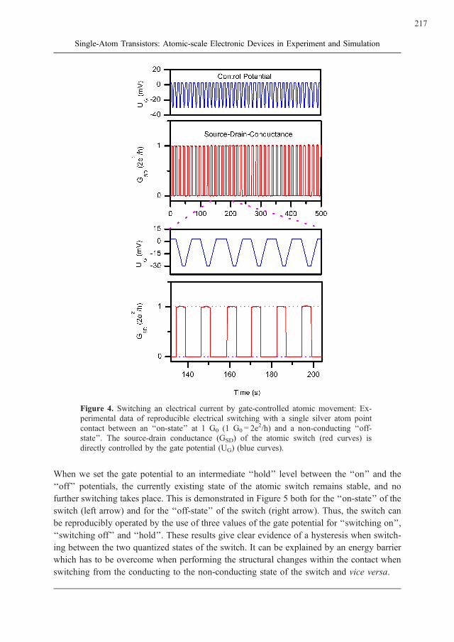
Figure 4. Switching an electrical current by gate-controlled atomic movement: Ex-
perimental data of reproducible electrical switching with a single silver atom point
contact between an ‘‘on-state’’ at 1 G0 (1 G0 = 2e2/h) and a non-conducting ‘‘off-
state’’. The source-drain conductance (GSD) of the atomic switch (red curves) is
directly controlled by the gate potential (UG) (blue curves).
When we set the gate potential to an intermediate ‘‘hold’’ level between the ‘‘on’’ and the
‘‘off’’ potentials, the currently existing state of the atomic switch remains stable, and no
further switching takes place. This is demonstrated in Figure 5 both for the ‘‘on-state’’ of the
switch (left arrow) and for the ‘‘off-state’’ of the switch (right arrow). Thus, the switch can
be reproducibly operated by the use of three values of the gate potential for ‘‘switching on’’,
‘‘switching off’’ and ‘‘hold’’. These results give clear evidence of a hysteresis when switch-
ing between the two quantized states of the switch. It can be explained by an energy barrier
which has to be overcome when performing the structural changes within the contact when
switching from the conducting to the non-conducting state of the switch and vice versa.
217
Single-Atom Transistors: Atomic-scale Electronic Devices in Experiment and Simulation
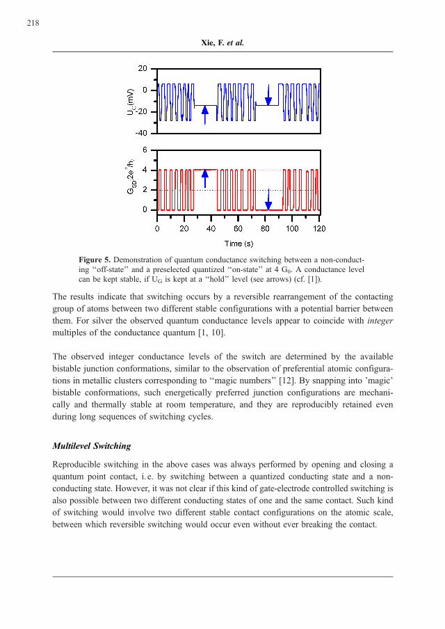
Figure 5. Demonstration of quantum conductance switching between a non-conduct-
ing ‘‘off-state’’ and a preselected quantized ‘‘on-state’’ at 4 G0. A conductance level
can be kept stable, if UG is kept at a ‘‘hold’’ level (see arrows) (cf. [1]).
The results indicate that switching occurs by a reversible rearrangement of the contacting
group of atoms between two different stable configurations with a potential barrier between
them. For silver the observed quantum conductance levels appear to coincide with integer
multiples of the conductance quantum [1, 10].
The observed integer conductance levels of the switch are determined by the available
bistable junction conformations, similar to the observation of preferential atomic configura-
tions in metallic clusters corresponding to ‘‘magic numbers’’ [12]. By snapping into ’magic’
bistable conformations, such energetically preferred junction configurations are mechani-
cally and thermally stable at room temperature, and they are reproducibly retained even
during long sequences of switching cycles.
Multilevel Switching
Reproducible switching in the above cases was always performed by opening and closing a
quantum point contact, i. e. by switching between a quantized conducting state and a non-
conducting state. However, it was not clear if this kind of gate-electrode controlled switching is
also possible between two different conducting states of one and the same contact. Such kind
of switching would involve two different stable contact configurations on the atomic scale,
between which reversible switching would occur even without ever breaking the contact.
218
Xie, F. et al.
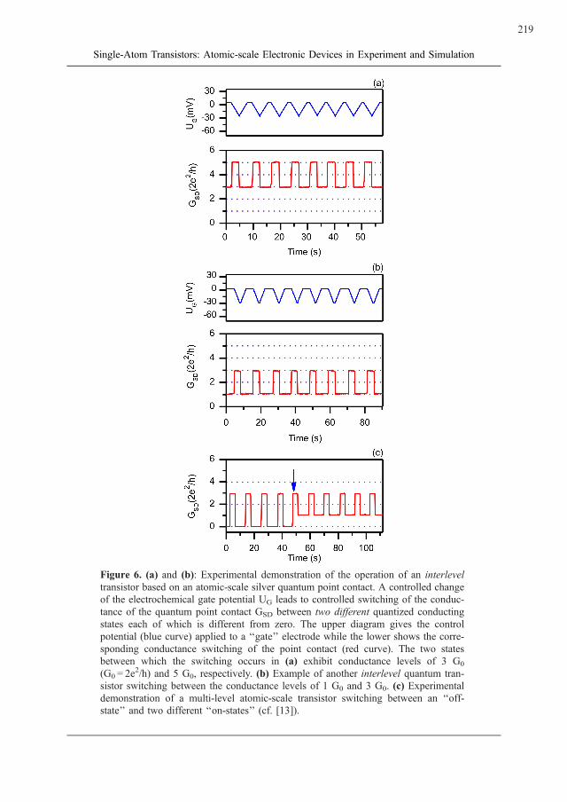
Figure 6. (a) and (b): Experimental demonstration of the operation of an interlevel
transistor based on an atomic-scale silver quantum point contact. A controlled change
of the electrochemical gate potential UG leads to controlled switching of the conduc-
tance of the quantum point contact GSD between two different quantized conducting
states each of which is different from zero. The upper diagram gives the control
potential (blue curve) applied to a ‘‘gate’’ electrode while the lower shows the corre-
sponding conductance switching of the point contact (red curve). The two states
between which the switching occurs in (a) exhibit conductance levels of 3 G0
(G0 = 2e2/h) and 5 G0, respectively. (b) Example of another interlevel quantum tran-
sistor switching between the conductance levels of 1 G0 and 3 G0. (c) Experimental
demonstration of a multi-level atomic-scale transistor switching between an ‘‘off-
state’’ and two different ‘‘on-states’’ (cf. [13]).
219
Single-Atom Transistors: Atomic-scale Electronic Devices in Experiment and Simulation
Such multi-level logics and storage devices on the atomic scale would be of great interest as
they allow a more efficient data storage and processing with a smaller number of logical
gates. By developing a modified procedure of fabrication, a multi-level atomic quantum
transistor was obtained, allowing the gate-controlled switching between different conducting
states.
Instead of setting the lower threshold where the dissolution process is stopped by the
computer, to a value near 0 G0, the lower threshold was set at a value above the desired
quantized conductance of the lower of the two ‘‘on-state’’ levels [13].
Figure 6 demonstrates the operation of such a two-level transistor: A controlled change of
the gate potential UG leads to a controlled switching of the conductance of the quantum
point contact between two different quantized conducting states (for details see caption of
Fig. 6). Sharp transitions are observed between the two levels. No intermediate steps or
staircase-like structures in conductance are observed in the diagram. The transitions are
instantaneous within the time resolution of the diagram of Figure 6 (50 ms).
Computer Simulations of the Switching Process
Reproducible switching between quantum conductance levels over many cycles cannot be
explained by conventional atom-by-atom deposition but requires a collective switching
mechanism. Our calculations have shown that only well-ordered junction geometries result
in integer multiples of the conductance quantum [10]. Neither partial dissolution of the
junction nor its controlled rupture yields the necessary atomic-scale memory effect. A more
detailed model of the structural [15, 16] and conductance [3, 17] properties of such junctions
is therefore required.
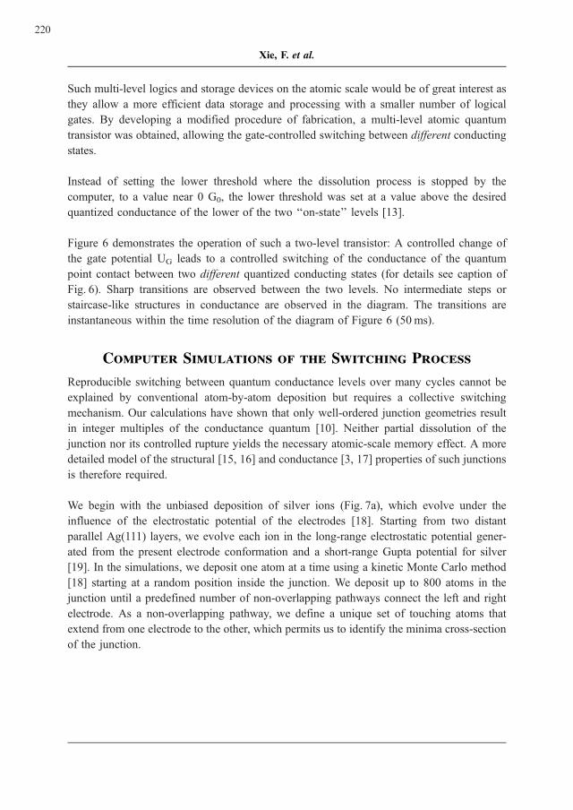
We begin with the unbiased deposition of silver ions (Fig. 7a), which evolve under the
influence of the electrostatic potential of the electrodes [18]. Starting from two distant
parallel Ag(111) layers, we evolve each ion in the long-range electrostatic potential gener-
ated from the present electrode conformation and a short-range Gupta potential for silver
[19]. In the simulations, we deposit one atom at a time using a kinetic Monte Carlo method
[18] starting at a random position inside the junction. We deposit up to 800 atoms in the
junction until a predefined number of non-overlapping pathways connect the left and right
electrode. As a non-overlapping pathway, we define a unique set of touching atoms that
extend from one electrode to the other, which permits us to identify the minima cross-section
of the junction.
220
Xie, F. et al.
Figure 7. Simulation of atomic point contact growth and switching process. (a) Snap-
shots of the deposition simulation. Upper row: The growth process starts with two
disconnected Ag(111) layers and stops, when a non-overlapping pathway with a
predefined number of silver atoms connects the electrodes. Lower row: Simulation
of the switching process reveals a bistable tip reconstruction process as the mechanism
underlying the reproducible switching of the conductance. During the simulation, we
kept the silver atoms marked in gray at their positions at the end of the deposition and
permitted the central cluster of atoms to evolve (blue and red atoms) under the
influence of the electrochemically induced pressure. The central silver atoms (red)
define the minimal cross-section. These atoms return with sub-Angstrom precision to
their original positions at the end of the switching cycle. (b) Difference in the com-
puted conductance between subsequent ‘‘on’’ conformations as a function of the
switching cycle for selected junctions of 1 G0, 2 G0, 3 G0, 4 G0, and 5 G0, respec-
tively. Junctions switch reproducibly for over 20 cycles between increasingly stable
‘‘on’’ and ‘‘off’’ conformations (training effect). (c) Variation of the computed con-
ductance of a 5 G0 switch during one ‘‘open-close’’ process. In agreement with the
experimental observations, we find asymmetric plateaus in the conductance curve, if
the switch is opened or closed. This can be traced back to the existence of several low-
energy pathways connecting the open and closed state (cf. [1]).
Next, we simulate the switching process: The change in the electrochemical potential
induces a change in the interface tension of the liquid-metal interface, making possible a
deformation of the junction geometry parallel to the junction axis. It is well-known that
changes in the electrochemical potential modulate the interfacial tension of the whole
electrode [20 – 22] which results in a mechanical strain on the junction. We simulate the
221
Single-Atom Transistors: Atomic-scale Electronic Devices in Experiment and Simulation
opening/closing cycle of a junction by evolving the atoms of a ‘‘central’’ cluster under the
influence of the electrochemical pressure. We assume that only the atoms in this region
move in the switching process, while most of the bulk material remains unchanged. The
central cluster comprises the atoms of the minimal cross-section connecting the two electro-
des and all atoms within a radius of 9.0 A around this central bottleneck. While the
electrodes gradually move apart/closer together, all atoms of the central cluster relax in
simulated annealing simulations generating a quasi-adiabatic path between the open and
the closed conformation.
Not surprisingly, the junction rips apart at some finite displacement from the equilibrium, an
effect also seen in break-junction experiments. For most junctions, this process is accom-
panied by a surface reorganization on at least one, but often both, tips of the electrode(s).
When we reverse the process, some junctions snap into the original atomistic conformation
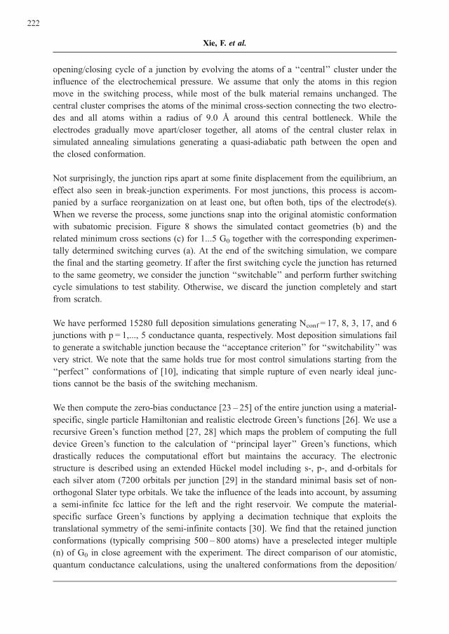
with subatomic precision. Figure 8 shows the simulated contact geometries (b) and the
related minimum cross sections (c) for 1...5 G0 together with the corresponding experimen-
tally determined switching curves (a). At the end of the switching simulation, we compare
the final and the starting geometry. If after the first switching cycle the junction has returned
to the same geometry, we consider the junction ‘‘switchable’’ and perform further switching
cycle simulations to test stability. Otherwise, we discard the junction completely and start
from scratch.
We have performed 15280 full deposition simulations generating Nconf = 17, 8, 3, 17, and 6
junctions with p = 1,..., 5 conductance quanta, respectively. Most deposition simulations fail
to generate a switchable junction because the ‘‘acceptance criterion’’ for ‘‘switchability’’ was
very strict. We note that the same holds true for most control simulations starting from the
‘‘perfect’’ conformations of [10], indicating that simple rupture of even nearly ideal junc-
tions cannot be the basis of the switching mechanism.
We then compute the zero-bias conductance [23 – 25] of the entire junction using a material-
specific, single particle Hamiltonian and realistic electrode Green’s functions [26]. We use a
recursive Green’s function method [27, 28] which maps the problem of computing the full
device Green’s function to the calculation of ‘‘principal layer’’ Green’s functions, which
drastically reduces the computational effort but maintains the accuracy. The electronic
structure is described using an extended Huckel model including s-, p-, and d-orbitals for
each silver atom (7200 orbitals per junction [29] in the standard minimal basis set of non-
orthogonal Slater type orbitals. We take the influence of the leads into account, by assuming
a semi-infinite fcc lattice for the left and the right reservoir. We compute the material-
specific surface Green’s functions by applying a decimation technique that exploits the
translational symmetry of the semi-infinite contacts [30]. We find that the retained junction
conformations (typically comprising 500 – 800 atoms) have a preselected integer multiple
(n) of G0 in close agreement with the experiment. The direct comparison of our atomistic,
quantum conductance calculations, using the unaltered conformations from the deposition/
222
Xie, F. et al.
switching simulations, with the experimental conductance measurements offers a strong
validation of the geometries generated in our deposition protocol. The observed agreement
between computed and measured conductance is impressive, because the conductance of
metallic wires is well-known to be strongly dependent on the geometry.
We have repeated this process up to 20 times for each junction (Fig. 7b) and observe a
‘‘training effect’’, in which the junction geometries become increasingly stable, alternating
between two bistable conformations. When re-computing the zero-bias conductance at the
end of switching cycle, we find the same value as for the original junction (to within ~0.05
G0). Because these observations result from completely unbiased simulations of junction
deposition and switching, they explain the observed reversible switching on the basis of the
generation of bistable contact geometries during the deposition cycle. If we consider the tip-
atoms at each side of the electrodes in the open junction, the equilibrium geometry of both
clusters depends on their environment. In the open junction, this environment is defined by
the remaining electrode atoms on one side, while in the closed junction, the tip-cluster of the
other electrode is also present. Our simulations demonstrate the existence of two stable
geometries for each cluster in both environmental conditions, respectively. Reversible
switching over many cycles is thus explained by reversible tip reorganization under the
influence of the gate potential, similar to induced surface reorganization [31 – 33]. While the
overall structure differs between junctions with the same conductance quantum from one
realization to the next (see Fig. 8b for representative examples), the minimal cross-section
that determines the conductance is largely conserved (Fig. 8c). When comparing the opening
process and the closing process of the junction, we observe asymmetric conductance curves
(see Fig. 7c), in agreement with experiment, resulting from irreversible low-energy pathways
between the open and the closed conformations.
These data rationalize the bistable reconfiguration of the electrode tips as the underlying
mechanism of the formation of nanoscale junctions with predefined levels of quantum
conductance. These levels are determined by the available bistable junction conformations,
similar to magic numbers for metal clusters [33] that are most likely material-specific. For
silver, the observed quantum conductance levels appear to coincide with integer multiples of
the conductance quantum. When we form a junction by halting the deposition process at a
non-integer multiple of G0 (both experimentally and in simulation), subsequent switching
cycles either converge to an integer conductance at a nearby level or destroy the junction. By
snapping into ‘‘magic’’ bistable conformations, junctions are mechanically and thermally
stable at room temperature for long sequences of switching cycles. This process is assisted
by the electrochemical environment but not intrinsically electrochemical: The reproducible
switching of large junctions by coordinated dissolution/regrowth of the junction is very
unlikely.
223
Single-Atom Transistors: Atomic-scale Electronic Devices in Experiment and Simulation
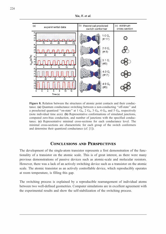
Figure 8. Relation between the structures of atomic point contacts and their conduc-
tance. (a) Quantum conductance switching between a non-conducting ‘‘off-state’’ and
a preselected quantized ‘‘on-state’’ at 1 G0, 2 G0, 3 G0, 4 G0, and 5 G0, respectively
(note individual time axis). (b) Representative conformations of simulated junctions,
computed zero-bias conduction, and number of junctions with the specified conduc-
tance. (c) Representative minimal cross-sections for each conductance level. The
minimal cross-sections are characteristic for each group of the switch conformers
and determine their quantized conductance (cf. [1]).
Conclusions and Perspectives
The development of the single-atom transistor represents a first demonstration of the func-
tionality of a transistor on the atomic scale. This is of great interest, as there were many
previous demonstrations of passive devices such as atomic-scale and molecular resistors.
However, there was a lack of an actively switching device such as a transistor on the atomic
scale. The atomic transistor as an actively controllable device, which reproducibly operates
at room temperature, is filling this gap.
The switching process is explained by a reproducible rearrangement of individual atoms
between two well-defined geometries. Computer simulations are in excellent agreement with
the experimental results and show the self-stabilization of the switching process.
224
Xie, F. et al.
Atomic transistors represent a new class of devices which show remarkable properties:
. They allow the switching of an electrical current by the geometrical relocation of
individual atoms rather than by locally changing electronic properties as done in
conventional transistors.
. They represent quantum switches, the levels between which the switching occurs
being given by fundamental laws of quantum mechanics.
. They are a first demonstration of an all-metal transistor without the use of any
semiconductor, the lack of a band gap allowing operation at very low voltages.
Such devices provide a number of advantages: They possess extremely nonlinear current-
voltage characteristics, desirable in many applications, and they can be manufactured using
conventional, abundant, inexpensive and non-toxic materials. At the same time, the devices
open perspectives for electronic switching at ultrafast frequencies: although the switching
time in our current investigations is limited by the response time of the electrodes (3 – 5
microseconds), the intrinsic operation time is expected to be limited by the atomic-scale
rearrangement within the junction (picoseconds), opening perspectives for ultrahigh fre-
quency operation. Because the switching process is achieved with very small gate potentials
in the millivolt range, the power consumption of such devices is by orders of magnitude
lower than that of conventional semiconductor-based electronics.
Although the development of the single-atom transistor just marks the beginning of actively
controlled electronics on the atomic scale, it opens fascinating perspectives for quantum
electronics and logics based on individual atoms. The development of a first, simple inte-
grated circuit [1, 14] and a multilevel quantum transistor [13] are first encouraging steps in
this direction.
Acknowledgment
This work was supported by the Deutsche Forschungsgemeinschaft within the DFG Centre
for Functional Nanostructures and by the Baden-Wurttemberg Foundation within the Net-
work of Excellence on Functional Nanostructures, Baden-Wurttemberg. Part of the experi-
mental section were reproduced with permission of Europhysics News (2010) [34], Figure 6
was reproduced with permission from Advanced Materials (Copyright 2010, Wiley-VCH)
[13], Figures 7 and 8 with permission from Nano Lett. (ACS, Copyright 2010) [1].
225
Single-Atom Transistors: Atomic-scale Electronic Devices in Experiment and Simulation
References
[1] Xie, F.-Q., Maul, R, Augenstein, A, Obermair, Ch., Starikov, E.B., Schon, G.,
Schimmel, Th., Wenzel, W. (2008) Nano Lett. 8:4493.
doi: 10.1021/nl802438c.
[2] Agraıt, N., Yeyati, A.L., van Ruitenbeek, J.M. (2003) Phys. Rep. 377:81.
doi: 10.1016/S0370-1573(02)00633-6.
[3] Scheer, E., Agrayt, N., Cuevas, N.J., Levy Yeyati, A., Ludoph, B., Martin-Rodero,
A., Rubio Bollinger, G., van Ruitenbeek, J.M., Urbina, C. (1998) Nature 394:154.
doi: 10.1038/28112.
[4] Mares, A.I., van Ruitenbeek, J.M. (2005) Phys. Rev. B 72:205402.
doi: 10.1103/PhysRevB.72.205402.
[5] Li, C. Z., Bogozi, A., Huang, W., Tao, N.J. (1999) Nanotechnology 10:221.
doi: 10.1088/0957-4484/10/2/320.
[6] Xie, F.-Q., Nittler, L., Obermair, Ch., Schimmel, Th. (2004) Phys. Rev. Lett.
93:128303.
doi: 10.1103/PhysRevLett.93.128303.
[7] Xie, F.-Q., Obermair, Ch., Schimmel, Th. (2004) Solid State Communications
132:437.
doi: 10.1016/j.ssc.2004.08.024.
[8] Smith, D.P.E. (1995) Science 269:371.
doi:10.1126/science.269.5222.371.
[9] Terabe, K., Hasegawa, T., Nakayama, T., Aono, M. (2005) Nature 433:47.
doi: 10.1038/nature03190.
[10] Xie, F.-Q., Maul, R., Brendelberger, S., Obermair, Ch., Starikow, E.B., Wenzel, W.,
Schon, G., Schimmel, Th. (2008) Appl. Phys. Lett. 93:043103.
doi: 10.1063/1.2955521.
[11] Xie, F.-Q., Obermair, Ch., Schimmel, Th. (2006) In: R. Gross et al. (eds.), Nanoscale
Devices - Fundamentals and Applications. Springer, p153.
[12] Huda M.N., Ray, A.K., (2003) Phys. Rev. A 67:013201.
doi: 10.1103/PhysRevA.67.013201.
[13] Xie, F.-Q., Maul, R., Obermair, Ch., Schon, G., Wenzel, W., Schimmel, Th. (2010)
Advanced Materials 22:2033.
doi: 10.1002/adma.200902953.
[14] Schimmel, Th., Xie, F.-Q., Obermair, Ch. Patent pending, US 2009195300.
226
Xie, F. et al.
[15] Pauly, F., Dreher, M., Viljas, J.K., Hafner, M., Cuevas, J.C., Nielaba, P. (2006) Phys.
Rev. B 74:235106.
doi: 10.1103/PhysRevB.74.235106.
[16] Yanson, I.K., Shklyarevskii, O.I., Csonka, S., van Kempen, H., Speller, S., Yanson,
A.I., van Ruitenbeek, J.M. (2005) Phys. Rev. Lett. 95:256806.
doi: 10.1103/PhysRevLett.95.256806.
[17] Yanson, A.I., Yanson, I.K., van Ruitenbeek, J.M. (2001) Phys. Rev. Lett. 87:216805.
doi: 10.1103/PhysRevLett.87.216805.
[18] Kwiatkowski, J.J., Nelson, J., Li, H., Bredas, J.L., Wenzel, W., Lennartz, C. (2008)
Phys. Chem. Chem. Phys. 10:1852.
doi: 10.1039/b719592c.
[19] Shao, X., Liu, X., Cai, W.J., (2005) J. Chem. Theory Comput. 1:762.
doi: 10.1021/ct049865j.
[20] Weissmuller, J., Viswanath, R.N., Kramer, D., Zimmer, P., Wurschum, R., Gleiter, H.
(2003) Science 300:312.
doi: 10.1126/science.1081024.
[21] Weigend, F., Evers, F., Weissmuller, J. (2006) Small 2:1497.
doi: 10.1002/smll.200600232.
[22] Inglesfield, J.E. (1985) Prog. Surf. Sci. 20:105.
doi: 10.1016/0079-6816(85)90007-3.
[23] Xue, Y., Datta, S., Ratner, M. (2002) Chem. Phys. 281:151.
doi: 10.1016/S0301-0104(02)00446-9.
[24] Heurich, J., Cuevas, J.C., Wenzel, W., Schon, G. (2002) Phys. Rev. Lett. 88:256803.
doi: 10.1103/PhysRevLett.88.256803.
[25] van Zalinge, H., Bates, A., Schiffrin, D.J., Starikov, E.B., Wenzel, W., Nichols, R.J.
(2006) Angew. Chem. 45:5499.
doi: 10.1002/anie.200601263.
[26] Jacob, T. (2007) Electrochim. Acta 52:2229.
doi: 10.1016/j.electacta.2006.03.114.
[27] Verges, J.A. (1999) Comput. Phys. Commun. 118:71.
doi: 10.1016/S0010-4655(99)00206-4.
[28] Maul, R., Wenzel, W. (2009) Phys. Rev. B 80:045424.
doi: 10.1103/PhysRevB.80.045424.
227
Single-Atom Transistors: Atomic-scale Electronic Devices in Experiment and Simulation
[29] Starikov, E.B., Tanaka, S., Kurita, N., Sengoku, Y., Natsume, T., Wenzel, W. (2005)
Eur. Phys. J. E 18:437.
doi: 10.1140/epje/e2005-00047-4.
[30] Damle, P., Ghosh, A.W., Datta, S. (2002) Chem. Phys. 281:171.
doi: 10.1016/S0301-0104(02)00496-2.
[31] Ohiso, A., Sugimoto, Y., Abe, M., Morita, S. (2007) Jpn. J. Appl. Phys. 46:5582.
doi: 10.1143/JJAP.46.5582.
[32] Ternes, M., Lutz, C.P., Hirjibehedin, C.F., Giessibl, F.J., Heinrich, A.J. (2008)
Science 319:1066.
doi: 10.1126/science.1150288.
[33] Huda, M.N., Ray, A.K. (2003) Phys. Rev. A 67:013201.
doi: 10.1103/PhysRevA.67.013201.
[34] Obermair, Ch., Xie, F.-Q., Schimmel, Th. (2010) Europhysics News 41:25.
doi: 10.1051/epn/2010403.
228
Xie, F. et al.