Embed Size (px)
Citation preview

RF and Protect ion Devices
BGA7L1N6
Appl icat ion Note AN351 Revision: Rev. 1.0
2013-11-13
Single-Band LTE LNA
Single Band LTE LNA BGA7L1N6 Support ing Band-5 (869-894 MHz) Using 0201 Components
BGA7L1N6 Single-Band LTE LNA for LTE Band-5 (869-894 MHz)
Application Note AN351, Rev. 1.0 2013-11-13 2 / 27
Application Note AN351
Revision History: 2013-11-13
Previous Revision:
Page Subjects (major changes since last revision)
Trademarks of Infineon Technologies AG
AURIX™, C166™, CanPAK™, CIPOS™, CIPURSE™, EconoPACK™, CoolMOS™, CoolSET™, CORECONTROL™, CROSSAVE™, DAVE™, DI-POL™, EasyPIM™, EconoBRIDGE™, EconoDUAL™, EconoPIM™, EconoPACK™, EiceDRIVER™, eupec™, FCOS™, HITFET™, HybridPACK™, I²RF™, ISOFACE™, IsoPACK™, MIPAQ™, ModSTACK™, my-d™, NovalithIC™, OptiMOS™, ORIGA™, POWERCODE™, PRIMARION™, PrimePACK™, PrimeSTACK™, PRO-SIL™, PROFET™, RASIC™, ReverSave™, SatRIC™, SIEGET™, SINDRION™, SIPMOS™, SmartLEWIS™, SOLID FLASH™, TEMPFET™, thinQ!™, TRENCHSTOP™, TriCore™.
Other Trademarks
Advance Design System™ (ADS) of Agilent Technologies, AMBA™, ARM™, MULTI-ICE™, KEIL™, PRIMECELL™, REALVIEW™, THUMB™, µVision™ of ARM Limited, UK. AUTOSAR™ is licensed by AUTOSAR development partnership. Bluetooth™ of Bluetooth SIG Inc. CAT-iq™ of DECT Forum. COLOSSUS™, FirstGPS™ of Trimble Navigation Ltd. EMV™ of EMVCo, LLC (Visa Holdings Inc.). EPCOS™ of Epcos AG. FLEXGO™ of Microsoft Corporation. FlexRay™ is licensed by FlexRay Consortium. HYPERTERMINAL™ of Hilgraeve Incorporated. IEC™ of Commission Electrotechnique Internationale. IrDA™ of Infrared Data Association Corporation. ISO™ of INTERNATIONAL ORGANIZATION FOR STANDARDIZATION. MATLAB™ of MathWorks, Inc. MAXIM™ of Maxim Integrated Products, Inc. MICROTEC™, NUCLEUS™ of Mentor Graphics Corporation. MIPI™ of MIPI Alliance, Inc. MIPS™ of MIPS Technologies, Inc., USA. muRata™ of MURATA MANUFACTURING CO., MICROWAVE OFFICE™ (MWO) of Applied Wave Research Inc., OmniVision™ of OmniVision Technologies, Inc. Openwave™ Openwave Systems Inc. RED HAT™ Red Hat, Inc. RFMD™ RF Micro Devices, Inc. SIRIUS™ of Sirius Satellite Radio Inc. SOLARIS™ of Sun Microsystems, Inc. SPANSION™ of Spansion LLC Ltd. Symbian™ of Symbian Software Limited. TAIYO YUDEN™ of Taiyo Yuden Co. TEAKLITE™ of CEVA, Inc. TEKTRONIX™ of Tektronix Inc. TOKO™ of TOKO KABUSHIKI KAISHA TA. UNIX™ of X/Open Company Limited. VERILOG™, PALLADIUM™ of Cadence Design Systems, Inc. VLYNQ™ of Texas Instruments Incorporated. VXWORKS™, WIND RIVER™ of WIND RIVER SYSTEMS, INC. ZETEX™ of Diodes Zetex Limited.
Last Trademarks Update 2011-11-11
BGA7L1N6 Single-Band LTE LNA for LTE Band-5 (869-894 MHz)
Introduction
Application Note AN351, Rev. 1.0 2013-11-13 3 / 27
Table of Content
1 Introduction ........................................................................................................................................ 4 1.1 Introduction About 3G and 4G ............................................................................................................. 4 1.2 Applications .......................................................................................................................................... 6 1.3 Infineon LNAs for 3G, 4G LTE and LTE-A Applications ...................................................................... 7
2 BGA7L1N6 Overview ....................................................................................................................... 10 2.1 Features ............................................................................................................................................. 10 2.2 Description ......................................................................................................................................... 10
3 Application Circuit and Performance Overview ............................................................................ 13 3.1 Summary of Measurement Results .................................................................................................... 13 3.2 BGA7L1N6 as LTE LNA for Band-5 (869-894 MHz) .......................................................................... 15 3.3 Schematics and Bill-of-Materials ........................................................................................................ 16
4 Measurement Graphs ...................................................................................................................... 17
5 Evaluation Board and Layout Information .................................................................................... 25
6 Authors .............................................................................................................................................. 26
7 Remark .............................................................................................................................................. 26
List of Figures
Figure 1 Example of Application Diagram of RF Front-End for 3G and 4G Systems. ....................................... 6 Figure 2 BGA7L1N6 in TSNP-6-2 .................................................................................................................... 10 Figure 3 Equivalent Circuit of BGA7L1N6 ........................................................................................................ 11 Figure 4 Package and Pin Connections of BGA7L1N6 .................................................................................... 11 Figure 5 Footprint Recommendation of BGA7L1N6 ........................................................................................ 12 Figure 6 Schematics of the BGA7L1N6 Application Circuit ............................................................................. 16 Figure 7 Insertion Power Gain (Narrowband) of the BGA7L1N6 for Band-5 Applications .............................. 17 Figure 8 Insertion Power Gain (Wideband) of the BGA7L1N6 for Band-5 Applications ................................. 17 Figure 9 Noise Figure of the BGA7L1N6 for Band-5 Applications ................................................................... 18 Figure 10 Input Matching of the BGA7L1N6 for Band-5 Applications ................................................................ 18 Figure 11 Input Matching (Smith Chart) of the BGA7L1N6 for Band-5 Applications ......................................... 19 Figure 12 Output Matching of the BGA7L1N6 for Band-5 Applications ............................................................. 19 Figure 13 Output Matching (Smith Chart) of the BGA7L1N6 for Band-5 Applications ...................................... 20 Figure 14 Reverse Isolation of the BGA7L1N6 for Band-5 Applications ............................................................ 20 Figure 15 Stability K-factor of the BGA7L1N6 for Band-5 Applications ............................................................. 21 Figure 16 Stability Mu1-factor of the BGA7L1N6 for Band-5 Applications ......................................................... 21 Figure 17 Stability Mu2-factor of the BGA7L1N6 for Band-5 Applications ......................................................... 22 Figure 18 Input 1dB Compression Point of the BGA7L1N6 for Band-5 Applications with Vcc=1.8 V ............... 22 Figure 19 Input 1dB Compression Point of the BGA7L1N6 for Band-5 Applications with Vcc=2.8 V ............... 23 Figure 20 Input 3
rd Intercept Point of the BGA7L1N6 for Band-5 Applications with Vcc=1.8 V ......................... 23
Figure 21 Input 3rd
Intercept Point of the BGA7L1N6 for Band-5 Applications with Vcc=2.8 V ......................... 24 Figure 22 Picture of Evaluation Board (overview) , BGA7L1N6 V1.0 ............................................................... 25 Figure 23 Picture of Evaluation Board (detailed view) ....................................................................................... 25 Figure 24 PCB Layer Stack ................................................................................................................................ 25
List of Tables
Table 1 LTE Band Assignment ......................................................................................................................... 4 Table 2 Infineon Product Portfolio of LNAs for 4G LTE and LTE-A Applications ............................................. 8 Table 3 Infineon Product Portfolio of LNAs for 3G and 4G Applications .......................................................... 9 Table 4 Pin Assignment of BGA7L1N6 ........................................................................................................... 12 Table 5 Electrical Characteristics at Room Temperature (TA = 25 °C) for ..................................................... 13 Table 6 Electrical Characteristics at Room Temperature (TA = 25 °C) for ...................................................... 14 Table 7 Bill-of-Materials ................................................................................................................................... 16
BGA7L1N6 Single-Band LTE LNA for LTE Band-5 (869-894 MHz)
Introduction
Application Note AN351, Rev. 1.0 2013-11-13 4 / 27
1 Introduction
1.1 Introduction About 3G and 4G
The mobile technologies for smartphones have seen tremendous growth in recent years. The
data rate required from mobile devices has increased significantly over the evolution modern
mobile technologies, starting from the first 3G/3.5G technologies (UMTS & WCDMA, HSPA &
HSPA+) to the recently 4G LTE-Advanced (LTE-A). LTE-A can support data rates of up to 1
Gbps.
Advanced technologies such as diversity Multiple Input Multiple Output (MIMO) and Carrier
Aggregation (CA) are adopted to achieve such higher data rate requirements. MIMO
technology, commonly referred as the diversity path in smartphones, has attracted attention
for the significant increasement in data throughput and link range without additional
bandwidth or increased transmit power. The technology supports scalable channel
bandwidth, between 1.4 and 20 MHz. The ability of 4G LTE to support bandwidths up to 20
MHz and to have more spectral efficiency by using high order modulation methods like QAM-
64 is of particular importance as the demand for higher wireless data speeds continues to
grow fast. Carrier aggregation used in LTE-Advanced combines up to 5 carriers and widens
bandwidths up to 100 MHz to increase the user rates, across FDD and TDD.
Countries all over the world have released various frequencies bands for the 4G
applications.Table 1 shows the band assignment for the LTE bands worldwide.
Table 1 LTE Band Assignment
Band No. Uplink Frequency Range Downlink Frequency Range Comment
1 1920-1980 MHz 2110-2170 MHz FDD
2 1850-1910 MHz 1930-1990 MHz FDD
3 1710-1785 MHz 1805-1880 MHz FDD
4 1710-1755 MHz 2110-2155 MHz FDD
5 824-849 MHz 869-894 MHz FDD
6 830-840 MHz 875-885 MHz FDD
7 2500-2570 MHz 2620-2690 MHz FDD
8 880-915 MHz 925-960 MHz FDD
9 1749.9-1784.9 MHz 1844.9-1879.9 MHz FDD
BGA7L1N6 Single-Band LTE LNA for LTE Band-5 (869-894 MHz)
Introduction
Application Note AN351, Rev. 1.0 2013-11-13 5 / 27
Table 1 LTE Band Assignment
Band No. Uplink Frequency Range Downlink Frequency Range Comment
10 1710-1770 MHz 2110-2170 MHz FDD
11 1427.9-1452.9 MHz 1475.9-1500.9 MHz FDD
12 698-716 MHz 728-746 MHz FDD
13 777-787 MHz 746-756 MHz FDD
14 788-798 MHz 758-768 MHz FDD
17 704-716 MHz 734-746 MHz FDD
18 815-830 MHz 860-875 MHz FDD
19 830-845 MHz 875-890 MHz FDD
20 832-862 MHz 791-821 MHz FDD
21 1447.9-1462.9 MHz 1495.9-1510.9 MHz FDD
22 3410-3500 MHz 3510-3600 MHz FDD
23 2000-2020 MHz 2180-2200 MHz FDD
24 1626.5-1660.5 MHz 1525-1559 MHz FDD
25 1850-1915 MHz 1930-1995 MHz FDD
26 814-849 MHz 859-894 MHz FDD
27 807-824 MHz 852-869 MHz FDD
28 703-748 MHz 758-803 MHz FDD
29 N/A 716-728 MHz FDD
33 1900-1920 MHz TDD
34 2010-2025 MHz TDD
35 1850-1910 MHz TDD
36 1930-1990 MHz TDD
37 1910-1930 MHz TDD
38 2570-2620 MHz TDD
39 1880-1920 MHz TDD
40 2300-2400 MHz TDD
41 2496-2690 MHz TDD
42 3400-3600 MHz TDD
43 3600-3800 MHz TDD
44 703-803 MHz TDD
In order to cover all the bands from different countries in a unique device, mobile phones and
data cards are usually equipped more bands and band combinations. Some typical examples
are quad-band combinations of band 1/2/5/8, 1/3/5/7 and 3/7/5/17. The frequency bands
used by TD-LTE are 3.4–3.6 GHz in Australia and UK, 2.57−2.62 GHz in the US and China,
2.545-2.575 GHz in Japan, and 2.3–2.4 GHz in India and Australia.
BGA7L1N6 Single-Band LTE LNA for LTE Band-5 (869-894 MHz)
Introduction
Application Note AN351, Rev. 1.0 2013-11-13 6 / 27
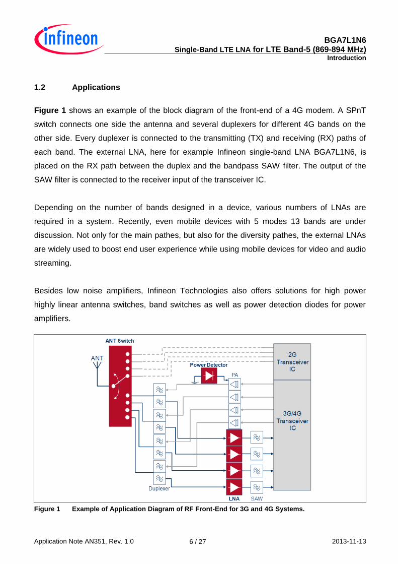
1.2 Applications
Figure 1 shows an example of the block diagram of the front-end of a 4G modem. A SPnT
switch connects one side the antenna and several duplexers for different 4G bands on the
other side. Every duplexer is connected to the transmitting (TX) and receiving (RX) paths of
each band. The external LNA, here for example Infineon single-band LNA BGA7L1N6, is
placed on the RX path between the duplex and the bandpass SAW filter. The output of the
SAW filter is connected to the receiver input of the transceiver IC.
Depending on the number of bands designed in a device, various numbers of LNAs are
required in a system. Recently, even mobile devices with 5 modes 13 bands are under
discussion. Not only for the main pathes, but also for the diversity pathes, the external LNAs
are widely used to boost end user experience while using mobile devices for video and audio
streaming.
Besides low noise amplifiers, Infineon Technologies also offers solutions for high power
highly linear antenna switches, band switches as well as power detection diodes for power
amplifiers.
Figure 1 Example of Application Diagram of RF Front-End for 3G and 4G Systems.
BGA7L1N6 Single-Band LTE LNA for LTE Band-5 (869-894 MHz)
Introduction
Application Note AN351, Rev. 1.0 2013-11-13 7 / 27
1.3 Infineon LNAs for 3G, 4G LTE and LTE-A Applications
With the increasing wireless data speed and with the extended link distance of mobile
phones and 4G data cards, the requirements on the sensitivity are much higher. Infineon
offers different kind of low noise amplifiers (LNAs) to support the customers for mobile
phones and data cards of 4G LTE and LTE-A to improve their system performance to meet
the requirements coming from the networks/service providers.
The benefits to use external LNAs in equipment for 4G LTE and LTE-A applications are:
- Flexible design to place the front-end components: due to the size constraint, the modem
antenna and the front-end can not be always put close to the transceiver IC. The path loss
in front of the integrated LNA on the transceiver IC increases the system noise figure
noticeably. An external LNA physically close to the antenna can help to eliminate the path
loss and reduce the system noise figure. Therefore the sensitivity can be improved by
several dB.
- Support RX carrier aggregation where two LNAs can be tuned on at the same time.
- Boost the sensitivity by reducing the system noise figure: external LNA has lower noise
figure than the integrated LNA on the transceiver IC.
- Bug fix to help the transceiver ICs to fulfill the system requirements.
- Increase the dynamic range of the power handling.
Infineon Technologies is the leading company with broad product portfolio to offer high
performance SiGe:C bipolar transistor LNAs and MMIC LNAs for various wireless
applications by using the industrial standard silicon process. The MMIC LNA portfolio
includes:
- New generation single band LTE LNAs like BGA7H1N6 for high-band (HB, 2300-2700
MHz), BGA7M1N6 for mid-band (MB, 1805-2200 MHz) and BGA7L1N6 for low-band (LB,
728-960 MHz) are available.
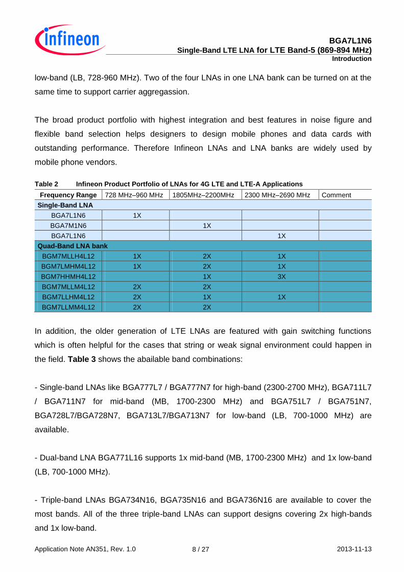
- New generation LTE LNA Banks are quad-band. Currently there are six different types of
these new LTE LNAs which are shown in Table 2. Each LNA bank combines four various
bands LNA from the high-band (HB, 2300-2700 MHz), mid-band (MB, 1805-2200 MHz) and
BGA7L1N6 Single-Band LTE LNA for LTE Band-5 (869-894 MHz)
Introduction
Application Note AN351, Rev. 1.0 2013-11-13 8 / 27
low-band (LB, 728-960 MHz). Two of the four LNAs in one LNA bank can be turned on at the
same time to support carrier aggregassion.
The broad product portfolio with highest integration and best features in noise figure and
flexible band selection helps designers to design mobile phones and data cards with
outstanding performance. Therefore Infineon LNAs and LNA banks are widely used by
mobile phone vendors.
Table 2 Infineon Product Portfolio of LNAs for 4G LTE and LTE-A Applications
Frequency Range 728 MHz–960 MHz 1805MHz–2200MHz 2300 MHz–2690 MHz Comment
Single-Band LNA
BGA7L1N6 1X
BGA7M1N6 1X
BGA7L1N6 1X
Quad-Band LNA bank
BGM7MLLH4L12 1X 2X 1X
BGM7LMHM4L12 1X 2X 1X
BGM7HHMH4L12 1X 3X
BGM7MLLM4L12 2X 2X
BGM7LLHM4L12 2X 1X 1X
BGM7LLMM4L12 2X 2X
In addition, the older generation of LTE LNAs are featured with gain switching functions
which is often helpful for the cases that string or weak signal environment could happen in
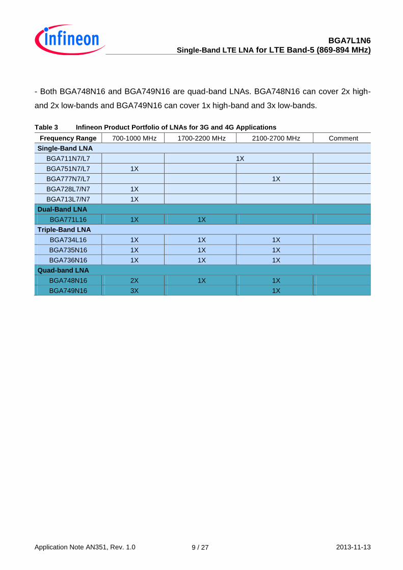
the field. Table 3 shows the abailable band combinations:
- Single-band LNAs like BGA777L7 / BGA777N7 for high-band (2300-2700 MHz), BGA711L7
/ BGA711N7 for mid-band (MB, 1700-2300 MHz) and BGA751L7 / BGA751N7,
BGA728L7/BGA728N7, BGA713L7/BGA713N7 for low-band (LB, 700-1000 MHz) are
available.
- Dual-band LNA BGA771L16 supports 1x mid-band (MB, 1700-2300 MHz) and 1x low-band
(LB, 700-1000 MHz).
- Triple-band LNAs BGA734N16, BGA735N16 and BGA736N16 are available to cover the
most bands. All of the three triple-band LNAs can support designs covering 2x high-bands
and 1x low-band.
BGA7L1N6 Single-Band LTE LNA for LTE Band-5 (869-894 MHz)
Application Note AN351, Rev. 1.0 2013-11-13 9 / 27
- Both BGA748N16 and BGA749N16 are quad-band LNAs. BGA748N16 can cover 2x high-
and 2x low-bands and BGA749N16 can cover 1x high-band and 3x low-bands.
Table 3 Infineon Product Portfolio of LNAs for 3G and 4G Applications
Frequency Range 700-1000 MHz 1700-2200 MHz 2100-2700 MHz Comment
Single-Band LNA
BGA711N7/L7 1X
BGA751N7/L7 1X
BGA777N7/L7 1X
BGA728L7/N7 1X
BGA713L7/N7 1X
Dual-Band LNA
BGA771L16 1X 1X
Triple-Band LNA
BGA734L16 1X 1X 1X
BGA735N16 1X 1X 1X
BGA736N16 1X 1X 1X
Quad-band LNA
BGA748N16 2X 1X 1X
BGA749N16 3X 1X
BGA7L1N6 Single-Band LTE LNA for LTE Band-5 (869-894 MHz)
BGA7L1N6 Overview
Application Note AN351, Rev. 1.0 2013-11-13 10 / 27
2 BGA7L1N6 Overview
2.1 Features
• Insertion power gain: 13.3 dB
• Low noise figure: 0.90 dB
• Low current consumption: 44 mA
• Operating frequencies: 716-960 MHz
• Supply voltage: 1.5 V to 3.6 V
• Digital on/off switch (1 V logic high level)
• Ultra small TSNP-6-2 leadless package (footprint:
0.7x1.1 mm2)
• B7HF Silicon Germanium technology
• RF output internally matched to 50 Ω
• Only 1 external SMD component necessary
• 2 kV HBM ESD protection (including AI-pin)
• Pb-free (RoHS compliant) package
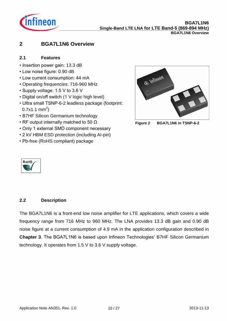
Figure 2 BGA7L1N6 in TSNP-6-2
2.2 Description
The BGA7L1N6 is a front-end low noise amplifier for LTE applications, which covers a wide
frequency range from 716 MHz to 960 MHz. The LNA provides 13.3 dB gain and 0.90 dB
noise figure at a current consumption of 4.9 mA in the application configuration described in
Chapter 3. The BGA7L1N6 is based upon Infineon Technologies‘ B7HF Silicon Germanium
technology. It operates from 1.5 V to 3.6 V supply voltage.

BGA7L1N6 Single-Band LTE LNA for LTE Band-5 (869-894 MHz)
BGA7L1N6 Overview
Application Note AN351, Rev. 1.0 2013-11-13 11 / 27
Figure 3 Equivalent Circuit of BGA7L1N6
Figure 4 Package and Pin Connections of BGA7L1N6

BGA7L1N6 Single-Band LTE LNA for LTE Band-5 (869-894 MHz)
BGA7L1N6 Overview
Application Note AN351, Rev. 1.0 2013-11-13 12 / 27
Figure 5 Footprint Recommendation of BGA7L1N6
Table 4 Pin Assignment of BGA7L1N6
Pin No. Symbol Function
1 GND Ground
2 VCC Supply voltage
3 AO LNA output
4 GND Ground
5 AI LNA input
6 PON Power on control
BGA7L1N6 Single-Band LTE LNA for LTE Band-5 (869-894 MHz)
Application Circuit and Performance Overview
Application Note AN351, Rev. 1.0 2013-11-13 13 / 27
3 Application Circuit and Performance Overview
Device: BGA7L1N6
Application: Single Band LTE LNA BGA7L1N6 Supporting Band-5 (869-894 MHz) Using 0201 Components
PCB Marking: BGA7x1N6 V1.0
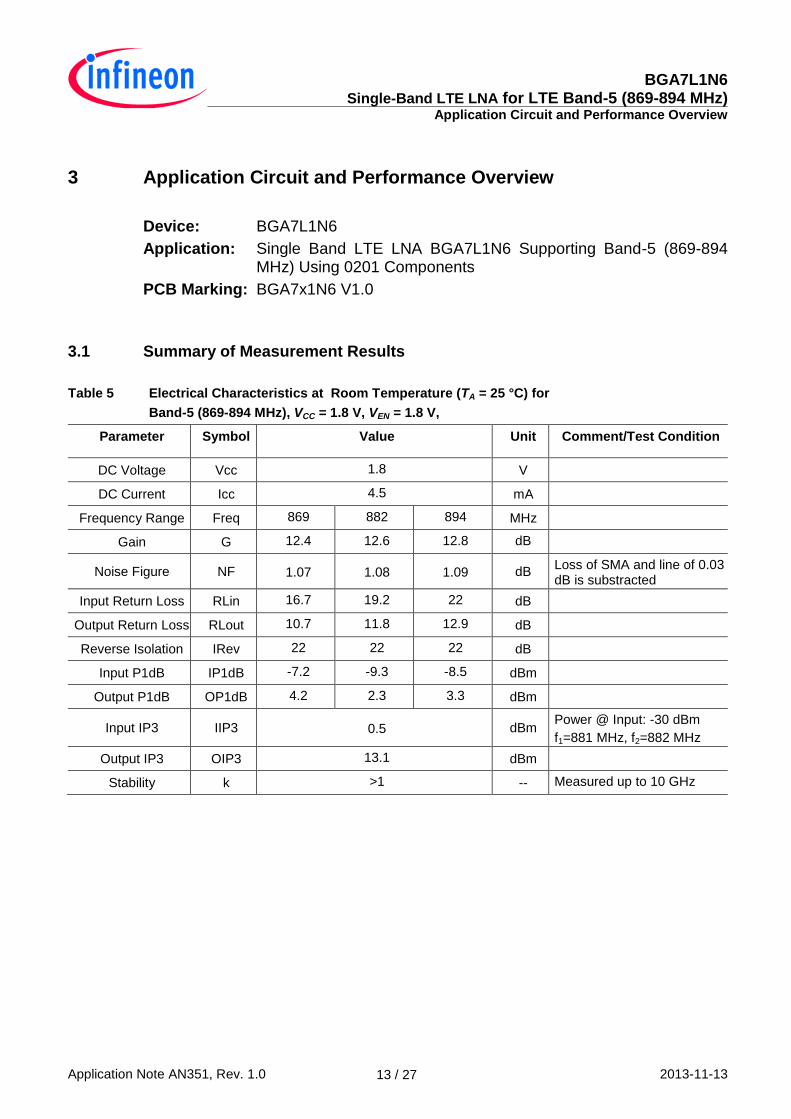
3.1 Summary of Measurement Results
Table 5 Electrical Characteristics at Room Temperature (TA = 25 °C) for
Band-5 (869-894 MHz), VCC = 1.8 V, VEN = 1.8 V,
Parameter Symbol Value Unit Comment/Test Condition
DC Voltage Vcc 1.8 V
DC Current Icc 4.5 mA
Frequency Range Freq 869 882 894 MHz
Gain G 12.4 12.6 12.8 dB
Noise Figure NF 1.07 1.08 1.09 dB Loss of SMA and line of 0.03 dB is substracted
Input Return Loss RLin 16.7 19.2 22 dB
Output Return Loss RLout 10.7 11.8 12.9 dB
Reverse Isolation IRev 22 22 22 dB
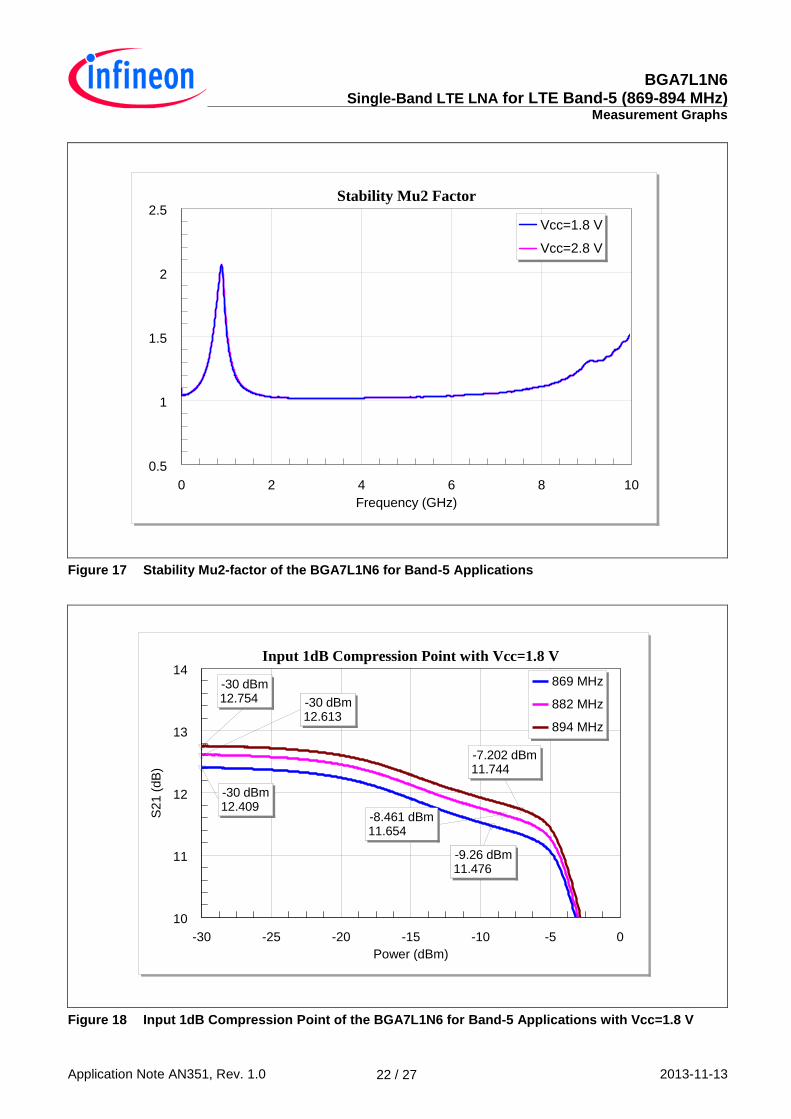
Input P1dB IP1dB -7.2 -9.3 -8.5 dBm
Output P1dB OP1dB 4.2 2.3 3.3 dBm
Input IP3 IIP3 0.5 dBm Power @ Input: -30 dBm
f1=881 MHz, f2=882 MHz
Output IP3 OIP3 13.1 dBm
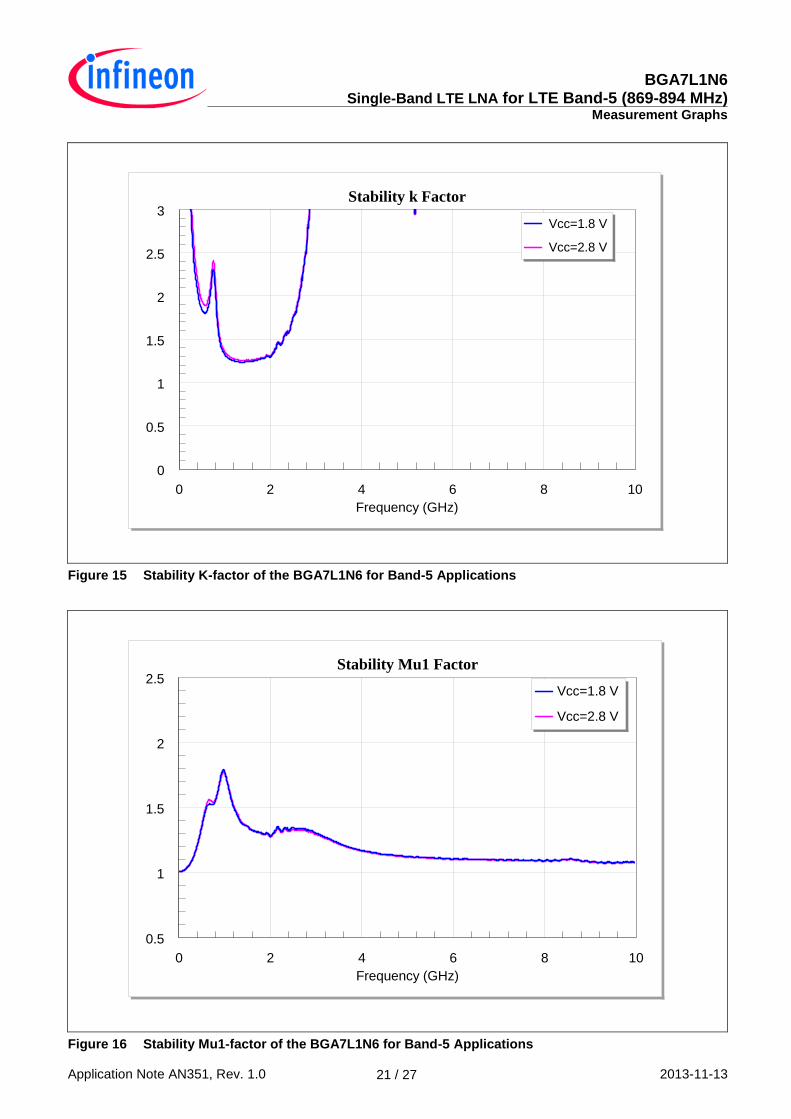
Stability k >1 -- Measured up to 10 GHz
BGA7L1N6 Single-Band LTE LNA for LTE Band-5 (869-894 MHz)
Application Circuit and Performance Overview
Application Note AN351, Rev. 1.0 2013-11-13 14 / 27
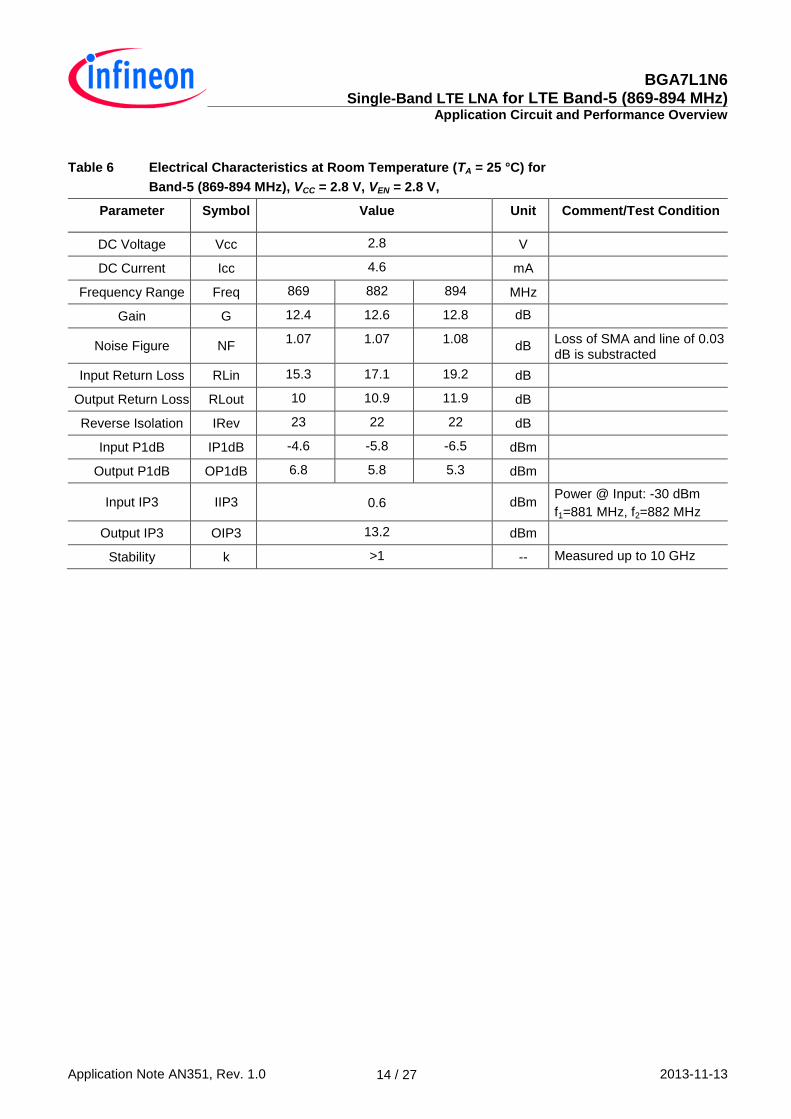
Table 6 Electrical Characteristics at Room Temperature (TA = 25 °C) for
Band-5 (869-894 MHz), VCC = 2.8 V, VEN = 2.8 V,
Parameter Symbol Value Unit Comment/Test Condition
DC Voltage Vcc 2.8 V
DC Current Icc 4.6 mA
Frequency Range Freq 869 882 894 MHz
Gain G 12.4 12.6 12.8 dB
Noise Figure NF 1.07 1.07 1.08
dB Loss of SMA and line of 0.03 dB is substracted
Input Return Loss RLin 15.3 17.1 19.2 dB
Output Return Loss RLout 10 10.9 11.9 dB
Reverse Isolation IRev 23 22 22 dB
Input P1dB IP1dB -4.6 -5.8 -6.5 dBm
Output P1dB OP1dB 6.8 5.8 5.3 dBm
Input IP3 IIP3 0.6 dBm Power @ Input: -30 dBm
f1=881 MHz, f2=882 MHz
Output IP3 OIP3 13.2 dBm
Stability k >1 -- Measured up to 10 GHz

BGA7L1N6 Single-Band LTE LNA for LTE Band-5 (869-894 MHz)
Application Circuit and Performance Overview
Application Note AN351, Rev. 1.0 2013-11-13 15 / 27
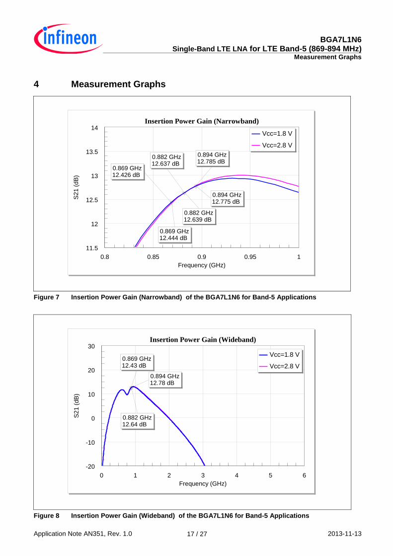
3.2 BGA7L1N6 as LTE LNA for Band-5 (869-894 MHz)
This application note focuses on the Infineon’s Single-band LTE LNA BGA7L1N6 tuned for the
band-5. It presents the performance of BGA7L1N6 with 1.8 V/2.8 V power supply with the
operating current of 4.6 mA.
The application circuit requires only one 0201 passive component. The component value is fine
tuned for optimal noise figure, gain, input and output matching. It has a gain of 12.8 dB. The
circuit achieves input return loss better than 15.3 dB, as well as output return loss better than 10
dB. At room temperature the noise figure is 1.1 dB (SMA and PCB losses are subtracted).
Furthermore, the circuit is measured unconditionally stable till 10 GHz. At Band-5, using two
tones spacing of 1 MHz, the output third order intercept point, OIP3 reaches 13.2 dBm. Input
P1dB of the BGA7L1N6 LNA is about –4.6 dBm for 894 MHz. All the measurements are done
with the standard evaluation board presented at the end of this application note.
BGA7L1N6 Single-Band LTE LNA for LTE Band-5 (869-894 MHz)
Application Note AN351, Rev. 1.0 2013-11-13 16 / 27
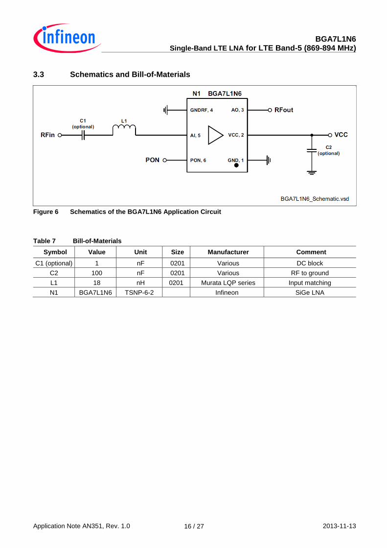
3.3 Schematics and Bill-of-Materials
Figure 6 Schematics of the BGA7L1N6 Application Circuit
Table 7 Bill-of-Materials
Symbol Value Unit Size Manufacturer Comment
C1 (optional) 1 nF 0201 Various DC block
C2 100 nF 0201 Various RF to ground
L1 18 nH 0201 Murata LQP series Input matching
N1 BGA7L1N6 TSNP-6-2 Infineon SiGe LNA
BGA7L1N6 Single-Band LTE LNA for LTE Band-5 (869-894 MHz)
Measurement Graphs
Application Note AN351, Rev. 1.0 2013-11-13 17 / 27
4 Measurement Graphs
Figure 7 Insertion Power Gain (Narrowband) of the BGA7L1N6 for Band-5 Applications
Figure 8 Insertion Power Gain (Wideband) of the BGA7L1N6 for Band-5 Applications
0.8 0.85 0.9 0.95 1
Frequency (GHz)
Insertion Power Gain (Narrowband)
11.5
12
12.5
13
13.5
14
S21 (
dB
)
0.894 GHz12.775 dB
0.894 GHz12.785 dB
0.882 GHz12.639 dB
0.869 GHz12.444 dB
0.882 GHz12.637 dB
0.869 GHz12.426 dB
Vcc=1.8 V
Vcc=2.8 V
0 1 2 3 4 5 6
Frequency (GHz)
Insertion Power Gain (Wideband)
-20
-10
0
10
20
30
S21 (
dB
)
0.894 GHz12.78 dB
0.882 GHz12.64 dB
0.869 GHz12.43 dB
Vcc=1.8 V
Vcc=2.8 V

BGA7L1N6 Single-Band LTE LNA for LTE Band-5 (869-894 MHz)
Measurement Graphs
Application Note AN351, Rev. 1.0 2013-11-13 18 / 27
Figure 9 Noise Figure of the BGA7L1N6 for Band-5 Applications
Figure 10 Input Matching of the BGA7L1N6 for Band-5 Applications
0.85 0.86 0.87 0.88 0.89 0.9
Frequency (GHz)
Noise Figure
1.03
1.05
1.07
1.09
1.11
1.13
NF
(d
B)
0.894 GHz1.08
0.894 GHz1.09
0.882 GHz1.07
0.882 GHz1.08
0.869 GHz1.07
Vcc=1.8 V
Vcc=2.8 V
0.8 0.85 0.9 0.95 1
Frequency (GHz)
Input Return Loss
-25
-20
-15
-10
-5
S1
1 (
dB
)
0.894 GHz-22.04 dB
0.894 GHz-19.24 dB
0.882 GHz-17.14 dB
0.882 GHz-19.15 dB
0.869 GHz-16.73 dB
0.869 GHz-15.27 dB
Vcc=1.8 V
Vcc=2.8 V

BGA7L1N6 Single-Band LTE LNA for LTE Band-5 (869-894 MHz)
Measurement Graphs
Application Note AN351, Rev. 1.0 2013-11-13 19 / 27
Figure 11 Input Matching (Smith Chart) of the BGA7L1N6 for Band-5 Applications
Figure 12 Output Matching of the BGA7L1N6 for Band-5 Applications
0 1.0
1.0
-1.0
10.0
10.0
-10.0
5.0
5.0
-5.0
2.0
2.0
-2.0
3.0
3.0
-3.0
4.0
4.0
-4.0
0.2
0.2
-0.2
0.4
0.4
-0.4
0.6
0.6
-0.6
0.8
0.8
-0.8
Input Return Loss (Smith Chart)Swp Max
1GHz
Swp Min
0.8GHz
0.869 GHzr 1.05x -0.30
0.882 GHzr 1.05x -0.22
0.894 GHzr 1.06x -0.15
0.894 GHzr 1.09x -0.21
0.882 GHzr 1.09x -0.28
0.869 GHzr 1.08x -0.35
Vcc=1.8 V
Vcc=2.8 V
0.8 0.85 0.9 0.95 1
Frequency (GHz)
Output Return Loss
-25
-20
-15
-10
-5
S2
2 (
dB
)
0.894 GHz-11.87 dB
0.894 GHz-12.85 dB
0.882 GHz-10.93 dB
0.882 GHz-11.75 dB
0.869 GHz-10.03 dB
0.869 GHz-10.71 dB
Vcc=1.8 V
Vcc=2.8 V

BGA7L1N6 Single-Band LTE LNA for LTE Band-5 (869-894 MHz)
Measurement Graphs
Application Note AN351, Rev. 1.0 2013-11-13 20 / 27
Figure 13 Output Matching (Smith Chart) of the BGA7L1N6 for Band-5 Applications
Figure 14 Reverse Isolation of the BGA7L1N6 for Band-5 Applications
0 1.0
1.0
-1.0
10.0
10.0
-10.0
5.0
5.0
-5.0
2.0
2.0
-2.0
3.0
3.0
-3.0
4.0
4.0
-4.0
0.2
0.2
-0.2
0.4
0.4
-0.4
0.6
0.6
-0.6
0.8
0.8
-0.8
Output Return Loss (Smith Chart)Swp Max
1GHz
Swp Min
0.8GHz
0.894 GHzr 0.63x 0.02
0.894 GHzr 0.60x 0.04
0.882 GHzr 0.59x -0.00
0.882 GHzr 0.56x 0.00
0.869 GHzr 0.55x -0.04
0.869 GHzr 0.52x -0.03
Vcc=1.8 V
Vcc=1.8 V
0.8 0.85 0.9 0.95 1
Frequency (GHz)
Reverse Isolation
-25
-24
-23
-22
-21
-20
S12 (
dB
) 0.894 GHz-22 dB
0.894 GHz-22 dB
0.882 GHz-22 dB
0.882 GHz-22 dB
0.869 GHz-22 dB
0.869 GHz-23 dB
Vcc=1.8 V
Vcc=2.8 V
BGA7L1N6 Single-Band LTE LNA for LTE Band-5 (869-894 MHz)
Measurement Graphs
Application Note AN351, Rev. 1.0 2013-11-13 21 / 27
Figure 15 Stability K-factor of the BGA7L1N6 for Band-5 Applications
Figure 16 Stability Mu1-factor of the BGA7L1N6 for Band-5 Applications
0 2 4 6 8 10
Frequency (GHz)
Stability k Factor
0
0.5
1
1.5
2
2.5
3 Vcc=1.8 V
Vcc=2.8 V
0 2 4 6 8 10
Frequency (GHz)
Stability Mu1 Factor
0.5
1
1.5
2
2.5Vcc=1.8 V
Vcc=2.8 V
BGA7L1N6 Single-Band LTE LNA for LTE Band-5 (869-894 MHz)
Measurement Graphs
Application Note AN351, Rev. 1.0 2013-11-13 22 / 27
Figure 17 Stability Mu2-factor of the BGA7L1N6 for Band-5 Applications
Figure 18 Input 1dB Compression Point of the BGA7L1N6 for Band-5 Applications with Vcc=1.8 V
0 2 4 6 8 10
Frequency (GHz)
Stability Mu2 Factor
0.5
1
1.5
2
2.5Vcc=1.8 V
Vcc=2.8 V
-30 -25 -20 -15 -10 -5 0
Power (dBm)
Input 1dB Compression Point with Vcc=1.8 V
10
11
12
13
14
S2
1 (
dB
)
-9.26 dBm11.476
-30 dBm12.409
-8.461 dBm11.654
-30 dBm12.613
-7.202 dBm11.744
-30 dBm12.754
869 MHz
882 MHz
894 MHz
BGA7L1N6 Single-Band LTE LNA for LTE Band-5 (869-894 MHz)
Measurement Graphs
Application Note AN351, Rev. 1.0 2013-11-13 23 / 27
Figure 19 Input 1dB Compression Point of the BGA7L1N6 for Band-5 Applications with Vcc=2.8 V
Figure 20 Input 3rd
Intercept Point of the BGA7L1N6 for Band-5 Applications with Vcc=1.8 V
-30 -25 -20 -15 -10 -5 0
Power (dBm)
Input 1dB Compression Point with Vcc=2.8 V
10
11
12
13
14
S2
1 (
dB
)
-6.533 dBm11.4
-30 dBm12.4
-5.849 dBm11.608
-30 dBm12.608
-4.649 dBm11.758
-30 dBm12.764
869 MHz
882 MHz
894 MHz
0.879 0.88 0.881 0.882 0.883 0.884
Frequency (GHz)
Intermodulation for Band-5 with Vcc=1.8 V
-120
-100
-80
-60
-40
-20
0
Po
we
r (d
Bm
)
0.883 GHz-78.91
0.882 GHz-17.39
0.881 GHz-17.44
0.88 GHz-78.38

BGA7L1N6 Single-Band LTE LNA for LTE Band-5 (869-894 MHz)
Measurement Graphs
Application Note AN351, Rev. 1.0 2013-11-13 24 / 27
Figure 21 Input 3rd
Intercept Point of the BGA7L1N6 for Band-5 Applications with Vcc=2.8 V
0.879 0.88 0.881 0.882 0.883 0.884
Frequency (GHz)
Intermodulation for Band-5 with Vcc=2.8 V
-120
-100
-80
-60
-40
-20
0
Po
wer
(dB
m)
0.883 GHz-79.06
0.882 GHz-17.41
0.881 GHz-17.45
0.88 GHz-78.73
BGA7L1N6 Single-Band LTE LNA for LTE Band-5 (869-894 MHz)
Evaluation Board and Layout Information
Application Note AN351, Rev. 1.0 2013-11-13 25 / 27
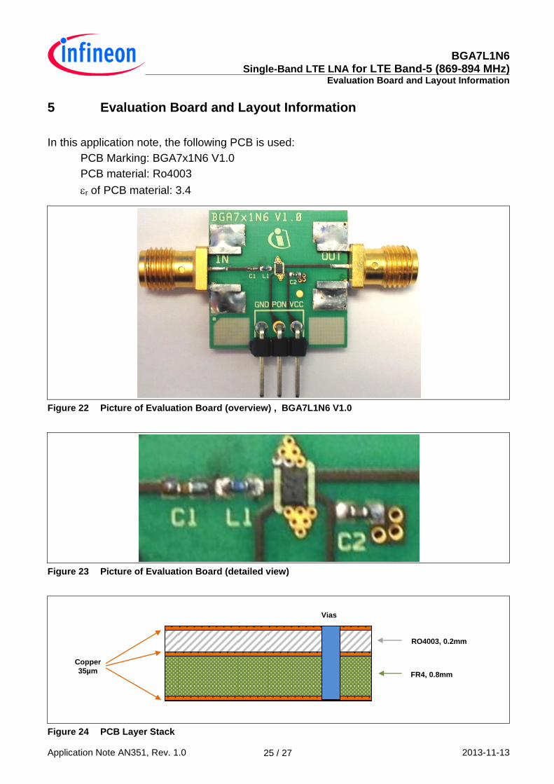
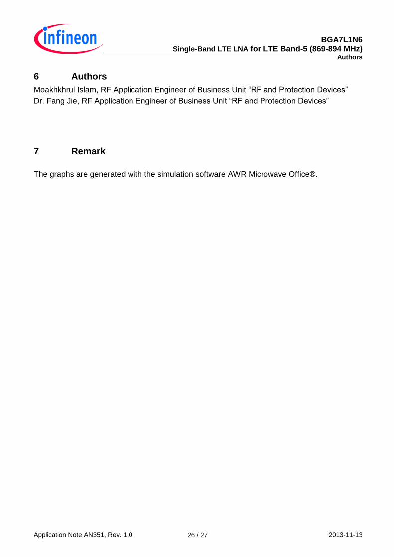
5 Evaluation Board and Layout Information
In this application note, the following PCB is used:
PCB Marking: BGA7x1N6 V1.0
PCB material: Ro4003
r of PCB material: 3.4
Figure 22 Picture of Evaluation Board (overview) , BGA7L1N6 V1.0
Figure 23 Picture of Evaluation Board (detailed view)
Figure 24 PCB Layer Stack
Copper
35µm
RO4003, 0.2mm
FR4, 0.8mm
Vias
BGA7L1N6 Single-Band LTE LNA for LTE Band-5 (869-894 MHz)
Authors
Application Note AN351, Rev. 1.0 2013-11-13 26 / 27
6 Authors
Moakhkhrul Islam, RF Application Engineer of Business Unit “RF and Protection Devices”
Dr. Fang Jie, RF Application Engineer of Business Unit “RF and Protection Devices”
7 Remark
The graphs are generated with the simulation software AWR Microwave Office®.

w w w . i n f i n e o n . c o m
Published by Infineon Technologies AG AN351


![Miniature Ka-band Low Noise Amplifier (Ka-LNA) · PDF fileNTS-PRM-14007Rev.2 Miniature Ka-band Low Noise Amplifier (Ka-LNA) 40 41 42 43 44 45 46 47 48 49 50 26.0 28.5 31.0 Gain [dB]](https://img.pdfslide.net/doc/110x75/5a7873ed7f8b9a87198b7cf8/miniature-ka-band-low-noise-amplifier-ka-lna-a-nts-prm-14007rev2-miniature.jpg)