Embed Size (px)
Citation preview
SIWave TrainingExercise 2
Trace with Via; Ground Plane with Apertures
2 Ansoft SIwave v1
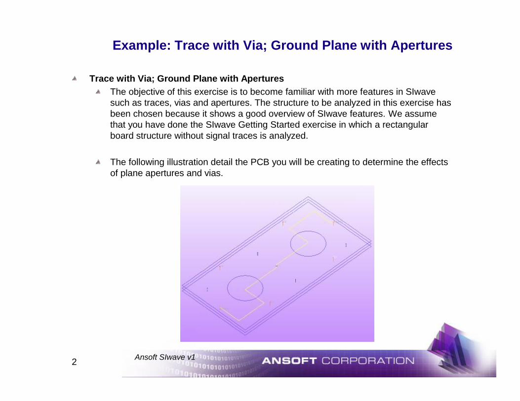
Example: Trace with Via; Ground Plane with Apertures
Trace with Via; Ground Plane with AperturesThe objective of this exercise is to become familiar with more features in SIwave such as traces, vias and apertures. The structure to be analyzed in this exercise has been chosen because it shows a good overview of SIwave features. We assume that you have done the SIwave Getting Started exercise in which a rectangular board structure without signal traces is analyzed.
The following illustration detail the PCB you will be creating to determine the effects of plane apertures and vias.

3 Ansoft SIwave v1
Notice
Notice:The information contained in this document is subject to change without notice.
Ansoft makes no warranty of any kind with regards to this material, including, but not limited to, the implied warranties of merchantability and fitness for a particular purpose. Ansoft shall not be liable for errors contained herein or for incidental or consequential damages in connections with the furnishing, performance, or use of this material.
This document contains proprietary information which is protected by copyright. All rights are reserved.
Ansoft CorporationFour Station SquareSuite 200Pittsburgh, PA 15219(412) 261-3200
Unix® is a registered trademark of UNIX System Laboratories, Inc.Windows™ is a trademark of Microsoft® Corporation.
© 1984— 2002 Ansoft Corporation
4 Ansoft SIwave v1
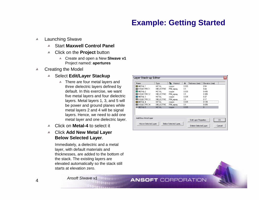
Example: Getting Started
Launching SIwaveStart Maxwell Control PanelClick on the Project button
Create and open a New SIwave v1Project named: apertures
Creating the ModelSelect Edit/Layer Stackup
There are four metal layers and three dielectric layers defined by default. In this exercise, we want five metal layers and four dielectric layers. Metal layers 1, 3, and 5 will be power and ground planes while metal layers 2 and 4 will be signal layers. Hence, we need to add one metal layer and one dielectric layer.
Click on Metal-4 to select itClick Add New Metal Layer Below Selected Layer.Immediately, a dielectric and a metal layer, with default materials and thicknesses, are added to the bottom of the stack. The existing layers are elevated automatically so the stack still starts at elevation zero.
5 Ansoft SIwave v1
Example: Layer Stackup
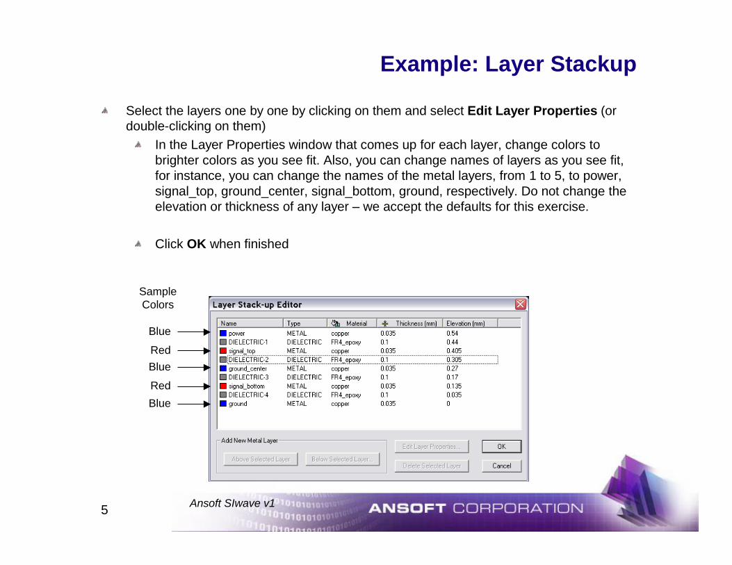
Select the layers one by one by clicking on them and select Edit Layer Properties (or double-clicking on them)
In the Layer Properties window that comes up for each layer, change colors to brighter colors as you see fit. Also, you can change names of layers as you see fit, for instance, you can change the names of the metal layers, from 1 to 5, to power, signal_top, ground_center, signal_bottom, ground, respectively. Do not change the elevation or thickness of any layer – we accept the defaults for this exercise.
Click OK when finished
Blue
Sample Colors
RedBlueRedBlue
6 Ansoft SIwave v1
Example: Model Construction
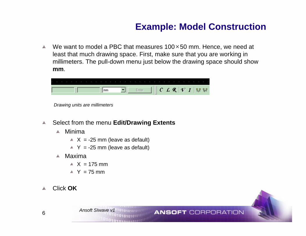
We want to model a PBC that measures 100× 50 mm. Hence, we need at least that much drawing space. First, make sure that you are working in millimeters. The pull-down menu just below the drawing space should show mm.
Select from the menu Edit/Drawing ExtentsMinima
X = -25 mm (leave as default)Y = -25 mm (leave as default)
MaximaX = 175 mmY = 75 mm
Click OK
Drawing units are millimeters
7 Ansoft SIwave v1
Example: Model Construction
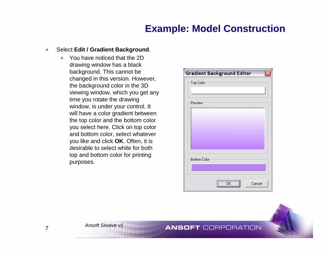
Select Edit / Gradient Background. You have noticed that the 2D drawing window has a black background. This cannot be changed in this version. However, the background color in the 3D viewing window, which you get any time you rotate the drawing window, is under your control. It will have a color gradient between the top color and the bottom color you select here. Click on top color and bottom color, select whatever you like and click OK. Often, it is desirable to select white for both top and bottom color for printing purposes.
8 Ansoft SIwave v1
Example: Planes
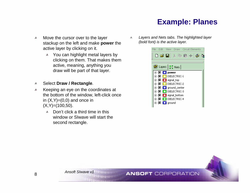
Move the cursor over to the layer stackup on the left and make power the active layer by clicking on it.
You can highlight metal layers by clicking on them. That makes them active, meaning, anything you draw will be part of that layer.
Select Draw / Rectangle. Keeping an eye on the coordinates at the bottom of the window, left-click once in (X,Y)=(0,0) and once in (X,Y)=(100,50).
Don’t click a third time in this window or SIwave will start the second rectangle.
Layers and Nets tabs. The highlighted layer (bold font) is the active layer.
9 Ansoft SIwave v1
Example: Planes
Move the cursor over to the layer stackup on the left and make ground-center the active layer by clicking on it. Its font will become bold.Move the cursor back into the drawing window. Notice the cursor is a cross there, indicating the Draw / Rectangle Mode is still active. This is confirmed by the status line at the very bottom of the SIwave window.Left-click once on (0,0) and once on (100,50) to create the ground plane in the center of the stack. Don’t click a third time in this window.Move the cursor over to the layer stackup on the left and make ground (at the bottom of the stack) the active layer by clicking on it. Its font will become bold.Left-click once on (0,0) and once on (100,50) to create the ground plane at the bottom of the stack. Don’t click a third time in this window.We are still in Draw / Rectangle Mode. To get out of this, locate the Draw Rectangle icon. It’s a toggle button; by clicking on it you get back into Viewing Mode.
10 Ansoft SIwave v1
Example: Planes
To learn how to correct a mistake, draw a rectangle you don’t want. Draw it completely outside the existing rectangles. Please do so now. Once you have the unwanted rectangle, toggle the Draw / Rectangle icon to get back in Viewing Mode. There are three ways to delete this rectangle.
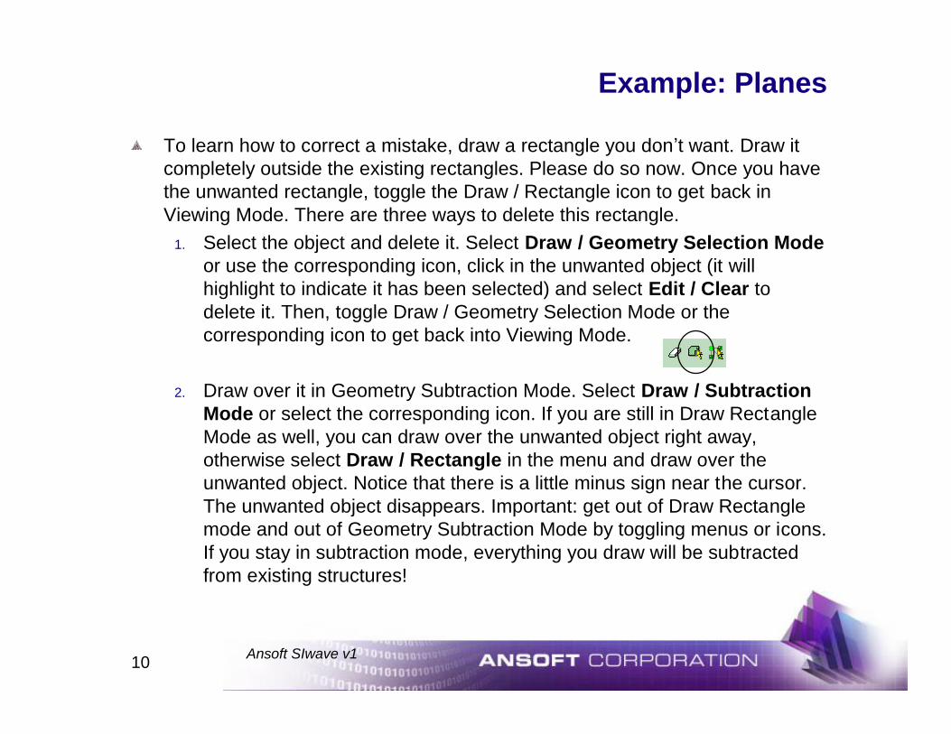
1. Select the object and delete it. Select Draw / Geometry Selection Mode or use the corresponding icon, click in the unwanted object (it will highlight to indicate it has been selected) and select Edit / Clear to delete it. Then, toggle Draw / Geometry Selection Mode or the corresponding icon to get back into Viewing Mode.
2. Draw over it in Geometry Subtraction Mode. Select Draw / Subtraction Mode or select the corresponding icon. If you are still in Draw Rectangle Mode as well, you can draw over the unwanted object right away, otherwise select Draw / Rectangle in the menu and draw over the unwanted object. Notice that there is a little minus sign near the cursor. The unwanted object disappears. Important: get out of Draw Rectangle mode and out of Geometry Subtraction Mode by toggling menus or icons. If you stay in subtraction mode, everything you draw will be subtracted from existing structures!
11 Ansoft SIwave v1
Example: Planes
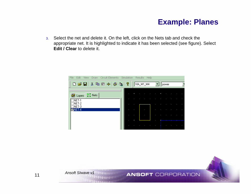
3. Select the net and delete it. On the left, click on the Nets tab and check the appropriate net. It is highlighted to indicate it has been selected (see figure). Select Edit / Clear to delete it.
12 Ansoft SIwave v1
Example: Apertures
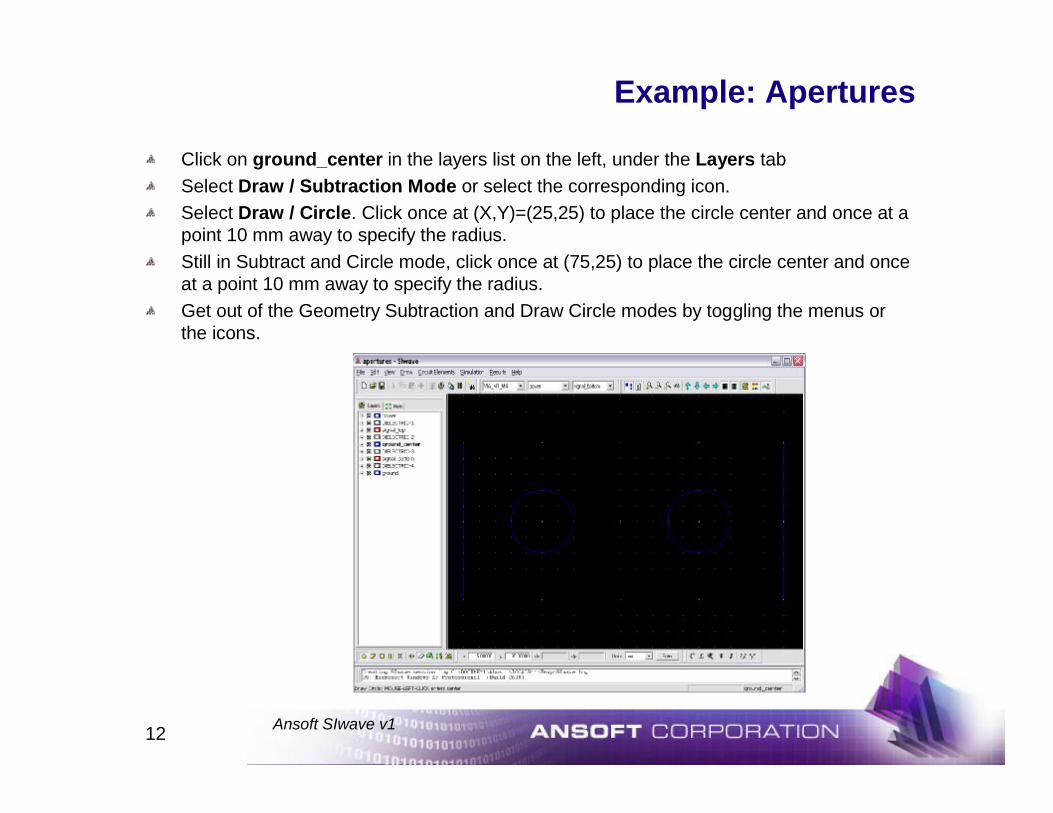
Click on ground_center in the layers list on the left, under the Layers tabSelect Draw / Subtraction Mode or select the corresponding icon.Select Draw / Circle. Click once at (X,Y)=(25,25) to place the circle center and once at a point 10 mm away to specify the radius. Still in Subtract and Circle mode, click once at (75,25) to place the circle center and once at a point 10 mm away to specify the radius.Get out of the Geometry Subtraction and Draw Circle modes by toggling the menus or the icons.
13 Ansoft SIwave v1
Setup: 3D View Mode
Select File/SaveAccept the default file name apertures.siw
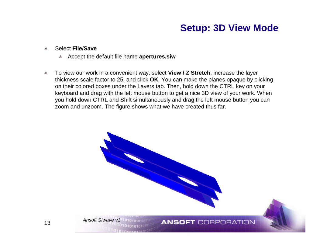
To view our work in a convenient way, select View / Z Stretch, increase the layer thickness scale factor to 25, and click OK. You can make the planes opaque by clicking on their colored boxes under the Layers tab. Then, hold down the CTRL key on your keyboard and drag with the left mouse button to get a nice 3D view of your work. When you hold down CTRL and Shift simultaneously and drag the left mouse button you can zoom and unzoom. The figure shows what we have created thus far.
14 Ansoft SIwave v1
Example: Traces
Switch to Top-down view by click on the iconEditing is disabled in 3D view
In this section, we will draw traces in both trace layers. They will be connected later by a via.
In the Layers list on the left, click on the second metal layer, signal_top, to make it active.Select Draw / Set Trace Width and choose a width of 0.1 mm, the same value as the thickness of the dielectric layer. Click OK
Note: in the process of drawing the trace, a right mouse click will also offer you the option of setting the width, at least for future sections of the trace. Once the trace has been created, you cannot go back and edit its width or coordinates in this version (1.0) of SIwave.
Select Draw / Trace. In the drawing window, your cursor changes from an arrow into a cross. Enter the following points by left-clicking on them; double-left-click for the last one: (X,Y) = (5,25) (5,10) (25,10) (25,25)(50,25).After double-clicking the last point, SIwave stops adding new segments, but you are still in Draw Tace Mode. As soon as you click anywhere in the drawing window, it will start creating the next trace.
15 Ansoft SIwave v1
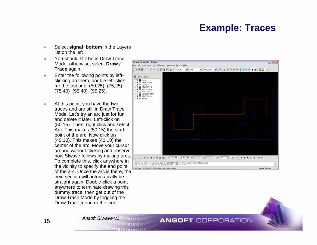
Example: Traces
Select signal_bottom in the Layers list on the leftYou should still be in Draw Trace Mode, otherwise, select Draw / Trace again.Enter the following points by left-clicking on them, double left-click for the last one: (50,25) (75,25) (75,40) (95,40) (95,25).
At this point, you have the two traces and are still in Draw Trace Mode. Let’s try an arc just for fun and delete it later. Left-click on (50,15). Then, right click and select Arc. This makes (50,15) the start point of the arc. Now click on (40,10). This makes (40,10) the center of the arc. Move your cursor around without clicking and observe how SIwave follows by making arcs. To complete this, click anywhere in the vicinity to specify the end point of the arc. Once the arc is there, the next section will automatically be straight again. Double-click a point anywhere to terminate drawing this dummy trace, then get out of the Draw Trace Mode by toggling the Draw Trace menu or the icon.
16 Ansoft SIwave v1
Example: Nets
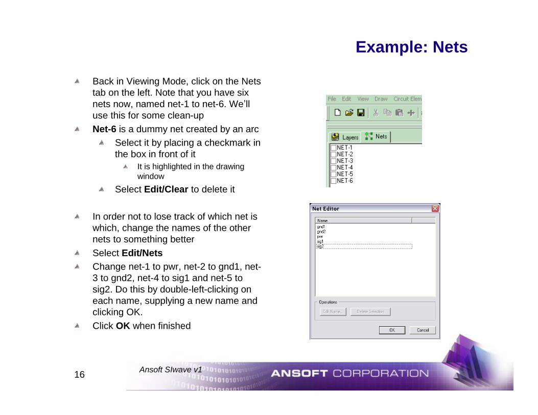
Back in Viewing Mode, click on the Nets tab on the left. Note that you have six nets now, named net-1 to net-6. We’ll use this for some clean-upNet-6 is a dummy net created by an arc
Select it by placing a checkmark in the box in front of it
It is highlighted in the drawing window
Select Edit/Clear to delete it
In order not to lose track of which net is which, change the names of the other nets to something betterSelect Edit/NetsChange net-1 to pwr, net-2 to gnd1, net-3 to gnd2, net-4 to sig1 and net-5 to sig2. Do this by double-left-clicking on each name, supplying a new name and clicking OK. Click OK when finished
17 Ansoft SIwave v1
Example: Model Construction
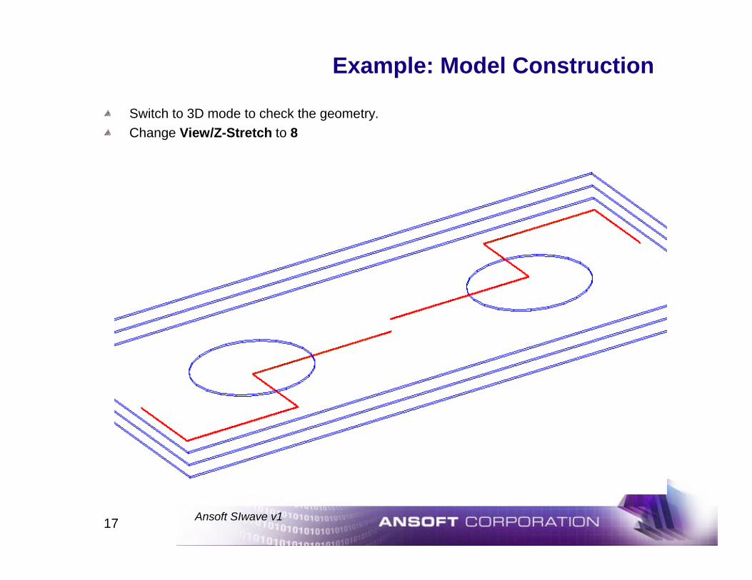
Switch to 3D mode to check the geometry.Change View/Z-Stretch to 8
18 Ansoft SIwave v1
Example: Vias
We will add vias to connect the two ground planes, and we will add one via to connect the two traces. Make sure you are in Top-Down Mode and that your entire model is visible. Before drawing anything, though, we have to make some specifications regarding the padstacks.
Select Edit / Padstacks. The Padstack Editor comes up. By default, it already has specifications for any pad and via we might want in SIwave’s default stackup with four metal layers and three dielectrics. It has not adjusted itself to the five metal layers and four dielectrics that we are working with now. We will add specifications for a via from the third to the fifth metal layer, that is, a via that connects the two ground planes.
In the Padstack Editor, select Add Padstack. A new padstack is created with name NEW_PADSTACK. Change this name to VIA_M3_M5 in the Name field
Do not click OK
19 Ansoft SIwave v1
Example: Vias
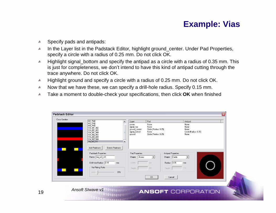
Specify pads and antipads:In the Layer list in the Padstack Editor, highlight ground_center. Under Pad Properties, specify a circle with a radius of 0.25 mm. Do not click OK.Highlight signal_bottom and specify the antipad as a circle with a radius of 0.35 mm. This is just for completeness, we don’t intend to have this kind of antipad cutting through the trace anywhere. Do not click OK.Highlight ground and specify a circle with a radius of 0.25 mm. Do not click OK.Now that we have these, we can specify a drill-hole radius. Specify 0.15 mm.Take a moment to double-check your specifications, then click OK when finished
20 Ansoft SIwave v1
Example: Vias
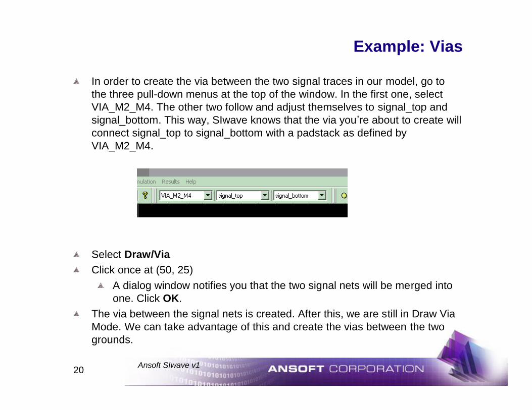
In order to create the via between the two signal traces in our model, go to the three pull-down menus at the top of the window. In the first one, select VIA_M2_M4. The other two follow and adjust themselves to signal_top and signal_bottom. This way, SIwave knows that the via you’re about to create will connect signal_top to signal_bottom with a padstack as defined by VIA_M2_M4.
Select Draw/ViaClick once at (50, 25)
A dialog window notifies you that the two signal nets will be merged into one. Click OK.
The via between the signal nets is created. After this, we are still in Draw Via Mode. We can take advantage of this and create the vias between the two grounds.
21 Ansoft SIwave v1
Example: Vias
In the left pull-down menu at the top of the window, where now VIA_M2_M4 is selected, select VIA_M3_M5. The other two pull-down menus follow and show ground_center and ground.Left-click once in (X,Y)=(50,10). Click OK in the dialog window that comes up.Left-click once in (50,40), once in (10,40) and once in (90,10). These are the vias we want. Just for exercise, create one undesired via by clicking in (5,30). Then, exit the Draw / Via Mode by toggling the menu item or the corresponding icon.
In order to get rid of the last via, go into Geometry Selection Mode by clicking the appropriate icon or by selecting Draw / Geometry Selection Mode. Then, carefully, bring the cursor on top of the undesired via. Zoom in if necessary. Left-click to select and highlight the via. Make sure planes are not highlighted at this point. Use Edit / Clear to delete via. Finally, go back into Viewing Mode by toggling the Geometry Selection Mode icon.
Select File/Save
22 Ansoft SIwave v1
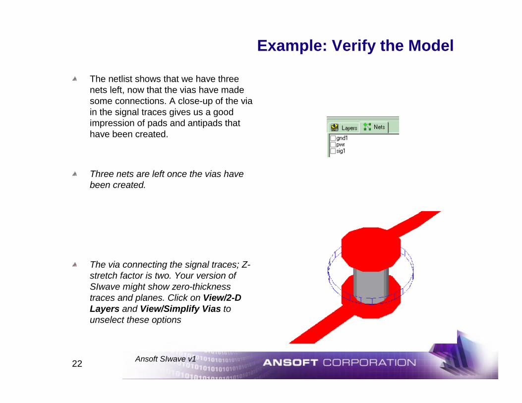
Example: Verify the Model
The netlist shows that we have three nets left, now that the vias have made some connections. A close-up of the via in the signal traces gives us a good impression of pads and antipads that have been created.
Three nets are left once the vias have been created.
The via connecting the signal traces; Z-stretch factor is two. Your version of SIwave might show zero-thickness traces and planes. Click on View/2-D Layers and View/Simplify Vias to unselect these options
23 Ansoft SIwave v1
Example: Decoupling Capacitors
Usually, there will be some decoupling capacitors between the power and ground nets. In this exercise, we will therefore create a few.Make sure you are in Top-Down Mode and that the entire model is visible. Select Circuit Elements / Capacitor and left-click twice on (X,Y)=(25,45) to place both terminals.
A window comes up that enables you to specify on which layers the terminals will reside. Select ‘power’for the positive terminal and ‘ground_center’for the negative terminal. Click OK. In the next window that comes up, you can specify the name, the capacitance, and also the parasitic inductance and resistance. Accept the defaults and click OK.
After this, the first capacitor is created. SIwave remains in Add Capacitor Mode.Add several more capacitors between layers ‘power’and ‘ground_center’, e.g. in (25,5) (for both terminals), in (75,45), in (75,5), and in any other location you like. Once you’re done, get out of the Add Capacitor Mode by toggling the menu item or the icon.
If you need to delete any capacitors, do the following:Select Draw / Circuit Element Selection Mode or use the corresponding icon.Place the cursor carefully over the center of the capacitor to be deleted (zoom if necessary) and left-click to select it. It will be highlighted.Use Edit / Clear to delete it.Toggle Draw / Circuit Element Selection Mode or the icon to get back into Viewing Mode.
24 Ansoft SIwave v1
Example: Resonance Modes Setup
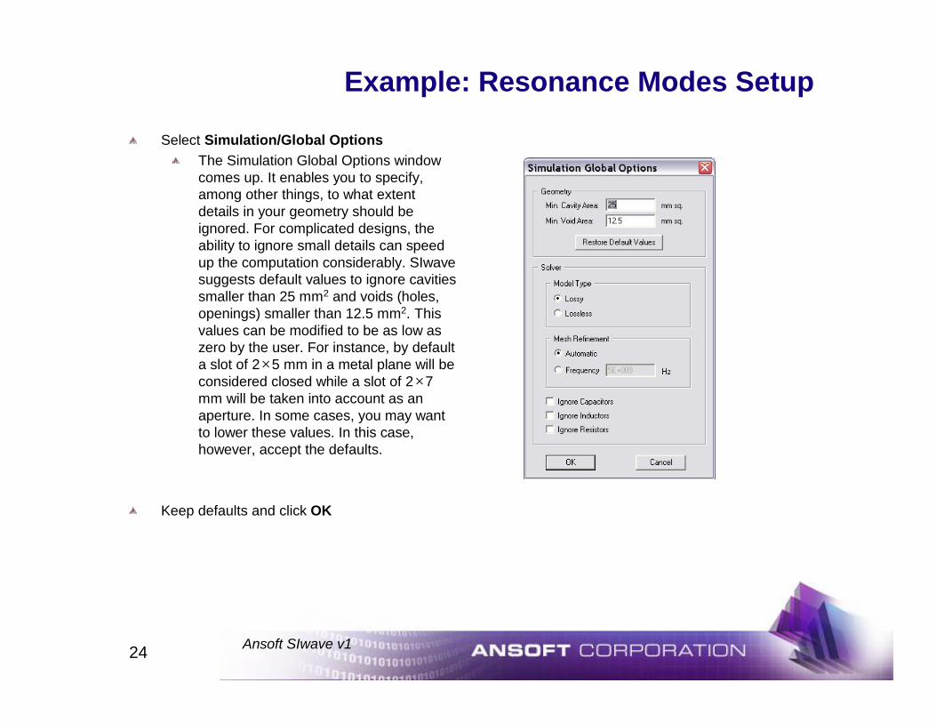
Select Simulation/Global OptionsThe Simulation Global Options window comes up. It enables you to specify, among other things, to what extent details in your geometry should be ignored. For complicated designs, the ability to ignore small details can speed up the computation considerably. SIwave suggests default values to ignore cavities smaller than 25 mm2 and voids (holes, openings) smaller than 12.5 mm2. This values can be modified to be as low as zero by the user. For instance, by defaulta slot of 2× 5 mm in a metal plane will be considered closed while a slot of 2× 7 mm will be taken into account as an aperture. In some cases, you may want to lower these values. In this case, however, accept the defaults.
Keep defaults and click OK
25 Ansoft SIwave v1
Example: Resonance Modes Setup
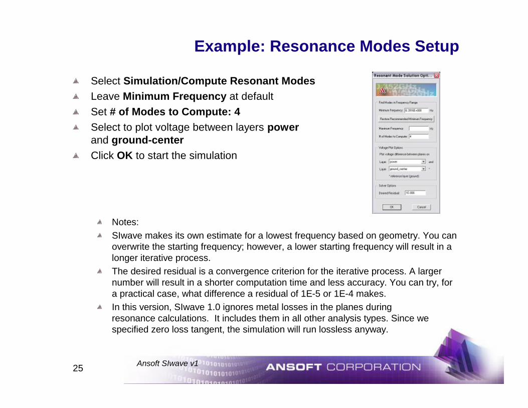
Select Simulation/Compute Resonant ModesLeave Minimum Frequency at defaultSet # of Modes to Compute: 4Select to plot voltage between layers power and ground-centerClick OK to start the simulation
Notes:SIwave makes its own estimate for a lowest frequency based on geometry. You can overwrite the starting frequency; however, a lower starting frequency will result in a longer iterative process.The desired residual is a convergence criterion for the iterative process. A larger number will result in a shorter computation time and less accuracy. You can try, for a practical case, what difference a residual of 1E-5 or 1E-4 makes.In this version, SIwave 1.0 ignores metal losses in the planes during resonance calculations. It includes them in all other analysis types. Since we specified zero loss tangent, the simulation will run lossless anyway.
26 Ansoft SIwave v1
Example: Resonant Modes
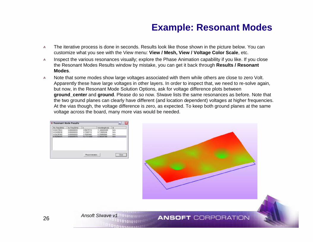
The iterative process is done in seconds. Results look like those shown in the picture below. You can customize what you see with the View menu: View / Mesh, View / Voltage Color Scale, etc. Inspect the various resonances visually; explore the Phase Animation capability if you like. If you close the Resonant Modes Results window by mistake, you can get it back through Results / Resonant Modes. Note that some modes show large voltages associated with them while others are close to zero Volt. Apparently these have large voltages in other layers. In order to inspect that, we need to re-solve again, but now, in the Resonant Mode Solution Options, ask for voltage difference plots between ground_center and ground. Please do so now. SIwave lists the same resonances as before. Note that the two ground planes can clearly have different (and location dependent) voltages at higher frequencies. At the vias though, the voltage difference is zero, as expected. To keep both ground planes at the same voltage across the board, many more vias would be needed.
27 Ansoft SIwave v1
Example: Drive the Signal Line and Compute Voltages
In this section, we will find out if, and to what extent, the signal line can excite any of the resonances we found in the previous section. Resonant modes may or may not get excited, depending whether a signal line couples to them or not.
Use the View menu to turn off any voltage surface plots, meshes, etc. Make sure SIwave is in the Top-Down View (use the Top-Down View icon) and that the entire model is visible (use View / Fit All).
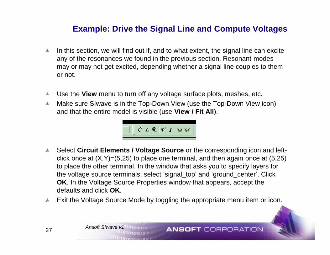
Select Circuit Elements / Voltage Source or the corresponding icon and left-click once at (X,Y)=(5,25) to place one terminal, and then again once at (5,25) to place the other terminal. In the window that asks you to specify layers for the voltage source terminals, select ‘signal_top’and ‘ground_center’. Click OK. In the Voltage Source Properties window that appears, accept the defaults and click OK.Exit the Voltage Source Mode by toggling the appropriate menu item or icon.
28 Ansoft SIwave v1
Example: Model Construction
We will terminate the other end of the signal line with a 50-Ohm resistor. Select Circuit Elements / Resistor and left-click once at (X,Y)=(95,25) to place one terminal, and then again once at (95,25) to place the other terminal. In the window that asks you to specify layers, select ‘signal_bottom’and ‘ground_center’. Click OK. In the next window, the Set Resistor Parameters window, specify 50 Ohm and click OK.Exit the Resistor Mode by toggling the appropriate menu item or the corresponding icon.
An important step is the selection of the signal traces to be included in the simulation. Planes are always included, signal traces only when you select them. This makes sense when you have a board with hundreds or thousands of traces. Therefore, under the Nets tab on the left, select sig1 by placing a checkmark in the box in front of it.Also, enable View / Voltage Surface Plot.
29 Ansoft SIwave v1
Example: Frequency Sweep Setup
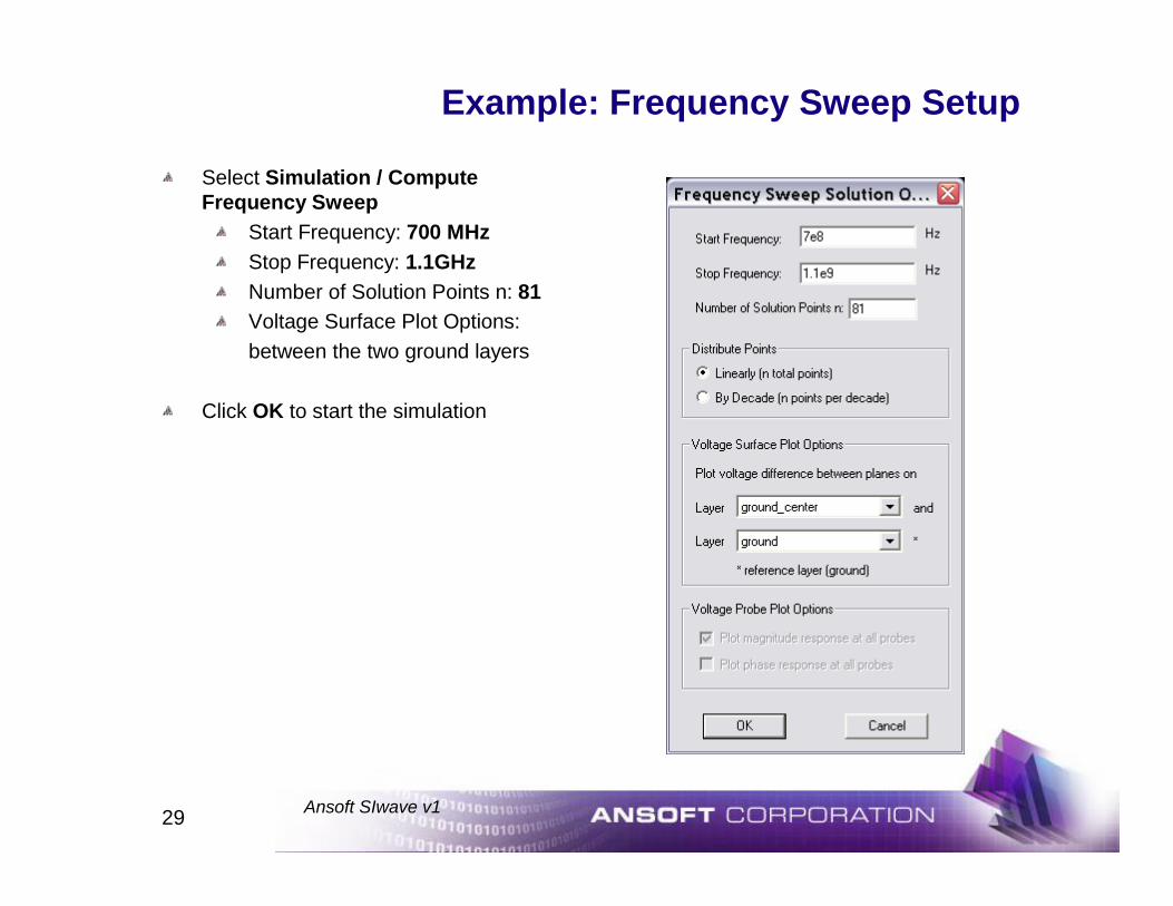
Select Simulation / Compute Frequency Sweep
Start Frequency: 700 MHzStop Frequency: 1.1GHzNumber of Solution Points n: 81 Voltage Surface Plot Options:between the two ground layers
Click OK to start the simulation
30 Ansoft SIwave v1
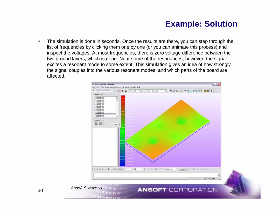
Example: Solution
The simulation is done in seconds. Once the results are there, you can step through the list of frequencies by clicking them one by one (or you can animate this process) and inspect the voltages. At most frequencies, there is zero voltage difference between the two ground layers, which is good. Near some of the resonances, however, the signal excites a resonant mode to some extent. This simulation gives an idea of how strongly the signal couples into the various resonant modes, and which parts of the board are affected.
31 Ansoft SIwave v1
Example: Solution
If you like, select Simulation / Compute Frequency Sweep again and ask for voltage differences between layers ‘power’and ‘ground_center’. Click OK. Again, the simulation is done in seconds. Scroll through the list of frequencies and determine which modes are excited between these two planes by the signal in the trace.
Note: If you have closed your Frequency Sweep Results window and want it back, you can select Results / Frequency Sweep.
In preparation for the next step, use the View menu to turn off the mesh, the voltage plot and the color scale. Also in preparation for the next step, we need to get rid of the voltage source and the resistor.
Under the Nets tab, deselect the signal line.Select Edit/Circuit Element ParametersSelect Resistors tabDelete resistor R1Select Voltage Sources tabDelete V1Click OK
Select File / Save to save your work.
32 Ansoft SIwave v1
Example: S-parameters
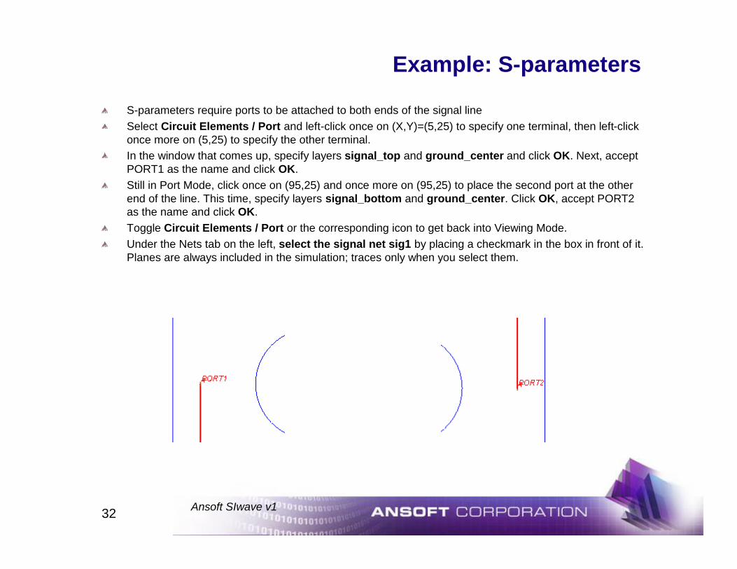
S-parameters require ports to be attached to both ends of the signal lineSelect Circuit Elements / Port and left-click once on (X,Y)=(5,25) to specify one terminal, then left-click once more on (5,25) to specify the other terminal. In the window that comes up, specify layers signal_top and ground_center and click OK. Next, accept PORT1 as the name and click OK. Still in Port Mode, click once on (95,25) and once more on (95,25) to place the second port at the other end of the line. This time, specify layers signal_bottom and ground_center. Click OK, accept PORT2 as the name and click OK.Toggle Circuit Elements / Port or the corresponding icon to get back into Viewing Mode.Under the Nets tab on the left, select the signal net sig1 by placing a checkmark in the box in front of it. Planes are always included in the simulation; traces only when you select them.
33 Ansoft SIwave v1
Example: S-parameters Setup
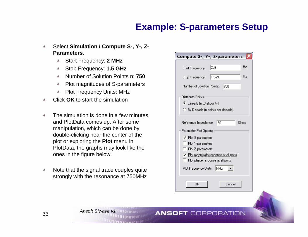
Select Simulation / Compute S-, Y-, Z-Parameters.
Start Frequency: 2 MHzStop Frequency: 1.5 GHzNumber of Solution Points n: 750 Plot magnitudes of S-parametersPlot Frequency Units: MHz
Click OK to start the simulation
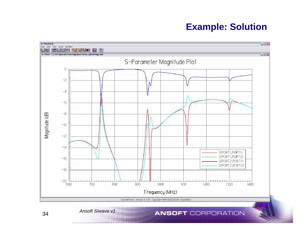
The simulation is done in a few minutes, and PlotData comes up. After some manipulation, which can be done by double-clicking near the center of the plot or exploring the Plot menu in PlotData, the graphs may look like the ones in the figure below.
Note that the signal trace couples quite strongly with the resonance at 750MHz
34 Ansoft SIwave v1
Example: Solution
35 Ansoft SIwave v1
Example: Full Wave SPICE
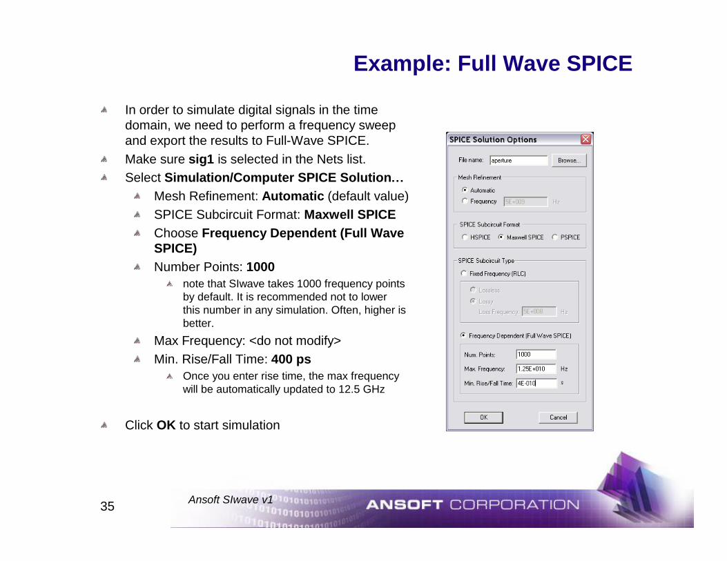
In order to simulate digital signals in the time domain, we need to perform a frequency sweep and export the results to Full-Wave SPICE. Make sure sig1 is selected in the Nets list. Select Simulation/Computer SPICE Solution…
Mesh Refinement: Automatic (default value)SPICE Subcircuit Format: Maxwell SPICEChoose Frequency Dependent (Full Wave SPICE)Number Points: 1000
note that SIwave takes 1000 frequency points by default. It is recommended not to lower this number in any simulation. Often, higher is better.
Max Frequency: <do not modify>Min. Rise/Fall Time: 400 ps
Once you enter rise time, the max frequency will be automatically updated to 12.5 GHz
Click OK to start simulation
36 Ansoft SIwave v1
Example: Full Wave Spice
The simulation takes several minutes. Once it’s done, click Close in the window that appears. Select File / Save
Launching Schematic CaptureStart the Maxwell Control Panel (if needed)Click the Projects button
Create and open a New Schematic Capture Project named: apertures_spiceIf several versions of the software are listed select the newestversion (Highest Release Number)
37 Ansoft SIwave v1
Example: Circuit Construction
Creating the CircuitSelect the menu item Add/Full Wave N-port Subcircuit
Click the Edit buttonClick the Import buttonFile Open: apertures.spcNote: If you cannot find the file, switch back to SIwave. Select Results/SPICE solution/SPICE subcircuit. Click Save As… . Verify that the .spc file is visible and find the location of this file. Click Cancel when doneClick OK
Select apertures in Definitions Loaded: windowReview the circuit in Definition:Click DoneClick OK
To place the new component, single click with the left mouse button to place the component. Move the mouse until the size and orientation of the component are acceptable. Click the left mouse button to finish placing the componentSince we only need to place one of these components, click the right mouse button and select Done
38 Ansoft SIwave v1
Example: Model Construction
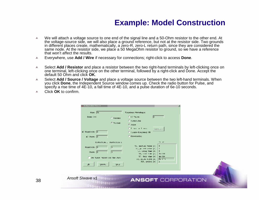
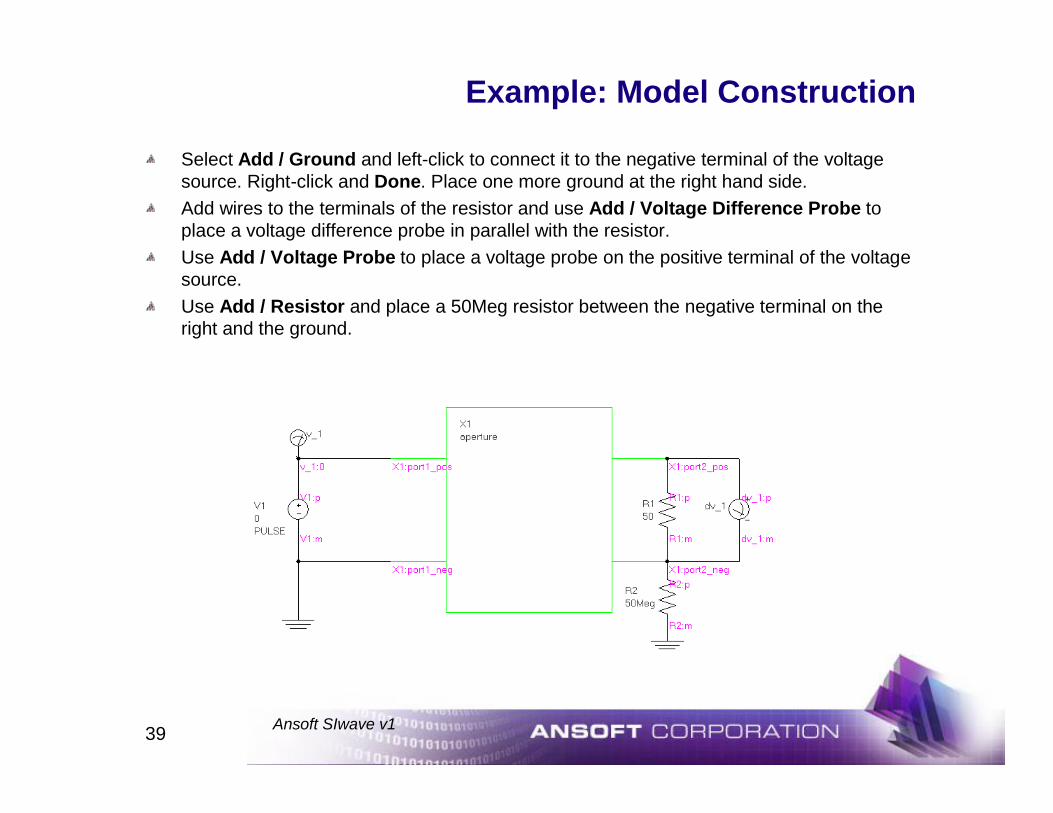
We will attach a voltage source to one end of the signal line and a 50-Ohm resistor to the other end. At the voltage-source side, we will also place a ground reference, but not at the resistor side. Two grounds in different places create, mathematically, a zero-R, zero-L return path, since they are considered the same node. At the resistor side, we place a 50 MegaOhm resistor to ground, so we have a reference that won’t affect the results. Everywhere, use Add / Wire if necessary for connections; right-click to access Done.
Select Add / Resistor and place a resistor between the two right-hand terminals by left-clicking once on one terminal, left-clicking once on the other terminal, followed by a right-click and Done. Accept the default 50 Ohm and click OK. Select Add / Source / Voltage and place a voltage source between the two left-hand terminals. When you click Done, the Independent Source window comes up. Check the radio button for Pulse, and specify a rise time of 4E-10, a fall time of 4E-10, and a pulse duration of 6e-10 seconds. Click OK to confirm.
39 Ansoft SIwave v1
Example: Model Construction
Select Add / Ground and left-click to connect it to the negative terminal of the voltage source. Right-click and Done. Place one more ground at the right hand side.Add wires to the terminals of the resistor and use Add / Voltage Difference Probe to place a voltage difference probe in parallel with the resistor.Use Add / Voltage Probe to place a voltage probe on the positive terminal of the voltage source.Use Add / Resistor and place a 50Meg resistor between the negative terminal on theright and the ground.
40 Ansoft SIwave v1
Example: Running SPICE
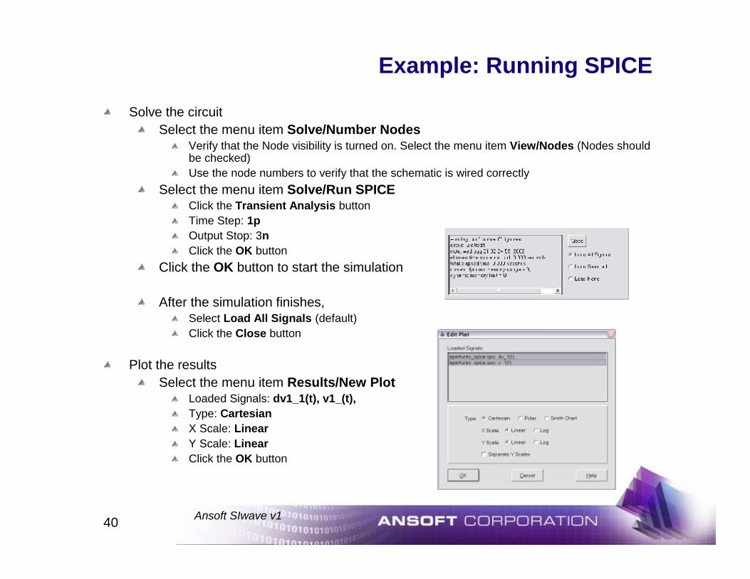
Solve the circuitSelect the menu item Solve/Number Nodes
Verify that the Node visibility is turned on. Select the menu item View/Nodes (Nodes should be checked)Use the node numbers to verify that the schematic is wired correctly
Select the menu item Solve/Run SPICEClick the Transient Analysis buttonTime Step: 1pOutput Stop: 3nClick the OK button
Click the OK button to start the simulation
After the simulation finishes,Select Load All Signals (default)Click the Close button
Plot the resultsSelect the menu item Results/New Plot
Loaded Signals: dv1_1(t), v1_(t),Type: CartesianX Scale: LinearY Scale: LinearClick the OK button
41 Ansoft SIwave v1
Example: Solution
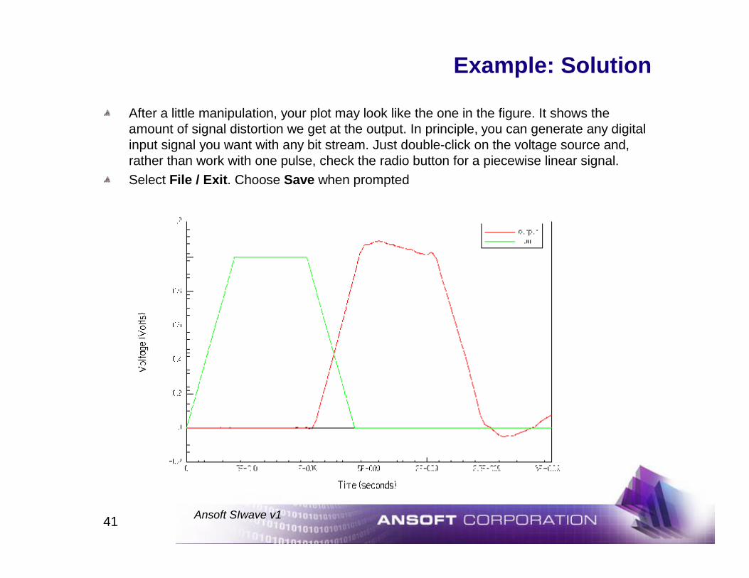
After a little manipulation, your plot may look like the one in the figure. It shows the amount of signal distortion we get at the output. In principle, you can generate any digital input signal you want with any bit stream. Just double-click on the voltage source and, rather than work with one pulse, check the radio button for a piecewise linear signal. Select File / Exit. Choose Save when prompted


![Ansys Siwave Brochure 14.0[1]](https://img.pdfslide.net/doc/110x75/544b459aaf7959a8438b51aa/ansys-siwave-brochure-1401.jpg)