Embed Size (px)
Citation preview
Product
Folder
Order
Now
Technical
Documents
Tools &
Software
Support &Community
An IMPORTANT NOTICE at the end of this data sheet addresses availability, warranty, changes, use in safety-critical applications,intellectual property matters and other important disclaimers. PRODUCTION DATA.
DAC38RF86, DAC38RF96DAC38RF87, DAC38RF97
SLASEF4B –FEBRUARY 2017–REVISED JULY 2017
DAC38RFxx Dual-Channel, Single-Ended,14-Bit, 6- and 9-GSPS, RF-Sampling DAC With JESD204B Interface and On-Chip GSM PLL
1
1 Features1• 14-Bit Resolution• Maximum DAC Sample Rate:
– 9.0 GSPS (DAC38RF86, DAC38RF96)– 6.2 GSPS (DAC38RF87, DAC38RF97)
• Key Specifications:– RF Full-Scale Output Power at 2.1 GHz:0 dBm– Spectral Performance, DAC38RF87/97
– fDAC = 5898.24 MSPS, fOUT = 2.14 GHz– WCDMA ACLR: 73 dBc– WCDMA alt-ACLR: 77 dBc
– Spectral Performance, DAC38RF86/96– fDAC = 8847.36 MSPS, fOUT = 3.7 GHz
– 20 MHz LTE ACLR: 66 dBc– fDAC = 9 GSPS, fOUT = 1.8 GHz, –6 dBFS
– IMD3 = 70 dBc (10-MHz tone spacing)• Dual-Band Digital Up-converter per DAC
– 6, 8, 10, 12, 16, 18, 20 or 24x Interpolation– 4 Independent NCOs With 48-Bit Resolution
• JESD204B Interface, Subclass 1– Support for Multichip Synchronization– Maximum Lane Rate: 12.5 Gbps
• Single-Ended Output With Integrated BalunCovering 700 MHz to 3800 MHz
• Internal PLL and VCO– DAC38RF86/96: fC(VCO) = 8.85 GHz– DAC38RF87/97: fC(VCO) = 5.90 GHz
• Power Dissipation: 1.4 to 2.2 W/ch• Power Supplies: –1.8 V, 1 V, 1.8 V• Package: 10 x 10 mm BGA, 0.8 mm Pitch, 144-
Balls
2 Applications• Wireless Communications• Communications Test Equipment• Arbitrary Waveform Generators• Military Software Defined Radios• Radar and Satellite Communications (SATCOM)
3 DescriptionThe DAC38RF86/96 is a family of high-performance,dual-channel, 14-bit, 9-GSPS, RF-sampling digital-to-analog converters (DACs) that are capable ofsynthesizing wideband signals from 0 to 4.5 GHz.The DAC38RF87/97 is also a family of high-performance, dual-channel, 14-bit, 6-GSPS, RF-sampling digital-to-analog converters (DACs) that arecapable of synthesizing wideband signals from 0 to 3GHz. A high dynamic range allows the DAC38RFxxfamily to generate signals for a wide range ofapplications including 3G/4G signals for wirelessbase-stations and radar.
The devices feature a low-power JESD204B Interfacewith up to 8 lanes with a maximum bit rate of 12.5Gbps allowing an input data rate of 1.25 GSPScomplex per channel. The DAC38RFxx provides twodigital up-converters per channel, with multipleoptions for interpolation rates. A digital quadraturemodulator with independent, frequency flexible NCOsare available to support multi-band operation. A GSMcompliant low phase noise PLL/VCO is integrated tosimplify the DAC sampling clock generation byallowing the use of a lower frequency reference clock
Device Information(1)
PART NUMBER OUTPUT TYPE NUMBER OFCHANNELS
DAC38RF86
Single ended 2DAC38RF96DAC38RF87DAC38RF97
(1) For all available device options, see the Device ComparisonTable.
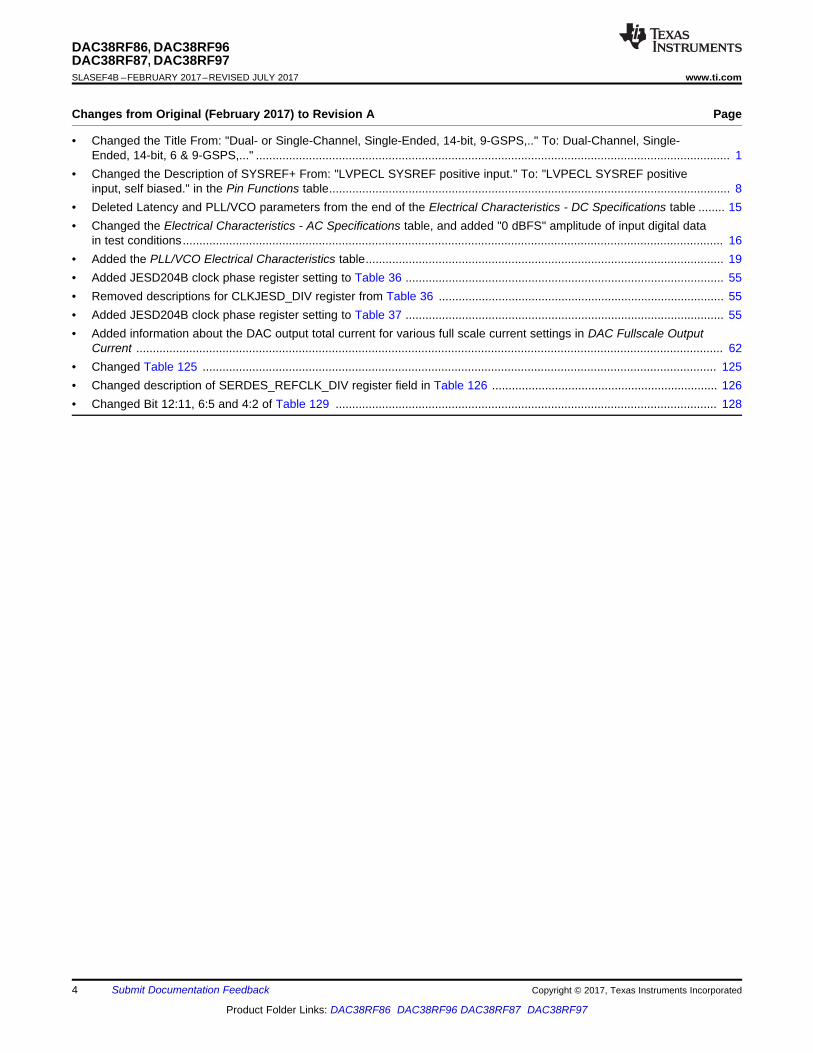
2x20-MHz LTE at 1.84 GHz and 2.14 GHz,800 MHz Span
2
DAC38RF86, DAC38RF96DAC38RF87, DAC38RF97SLASEF4B –FEBRUARY 2017–REVISED JULY 2017 www.ti.com
Product Folder Links: DAC38RF86 DAC38RF96 DAC38RF87 DAC38RF97
Submit Documentation Feedback Copyright © 2017, Texas Instruments Incorporated
Table of Contents1 Features .................................................................. 12 Applications ........................................................... 13 Description ............................................................. 14 Revision History..................................................... 25 Device Comparison Table ..................................... 56 Pin Configuration and Functions ......................... 67 Specifications......................................................... 9
7.1 Absolute Maximum Ratings ...................................... 97.2 ESD Ratings.............................................................. 97.3 Recommended Operating Conditions....................... 97.4 Thermal Information ................................................ 107.5 Electrical Characteristics - DC Specifications......... 107.6 Electrical Characteristics - Digital Specifications .... 137.7 Electrical Characteristics - AC Specifications ......... 167.8 PLL/VCO Electrical Characteristics ........................ 197.9 Timing Requirements .............................................. 207.10 Typical Characteristics, DAC38RF86 and
DAC38RF96 ............................................................ 218 Detailed Description ............................................ 27
8.1 Overview ................................................................. 278.2 Functional Block Diagrams ..................................... 27
8.3 Feature Description................................................. 298.4 Device Functional Modes........................................ 648.5 Register Maps ........................................................ 68
9 Application and Implementation ...................... 1309.1 Application Information.......................................... 1309.2 Typical Application: Multi-band Radio Frequency
Transmitter ............................................................ 13110 Power Supply Recommendations ................... 134
10.1 Power Supply Sequencing.................................. 13511 Layout................................................................. 135
11.1 Layout Guidelines ............................................... 13511.2 Layout Example .................................................. 137
12 Device and Documentation Support ............... 13812.1 Related Links ...................................................... 13812.2 Receiving Notification of Documentation
Updates.................................................................. 13812.3 Community Resources........................................ 13812.4 Trademarks ......................................................... 13812.5 Electrostatic Discharge Caution.......................... 13812.6 Glossary .............................................................. 138
13 Mechanical, Packaging, and OrderableInformation ......................................................... 138
4 Revision HistoryNOTE: Page numbers for previous revisions may differ from page numbers in the current version.
Changes from Revision A (April 2017) to Revision B Page
• Changed the Description ........................................................................................................................................................ 1• Changed the Device Information table ................................................................................................................................... 1• Changed From: alarm_out_pol To: alm_out_pol in ALARM pin description in the Pin Functions table ................................ 7• Changed the Description of pins A3, A4, A7, A6, A9, A10, A12, F11, F7, G6, G12, H5, H7, J6, J11 in the Pin
Functions table ....................................................................................................................................................................... 7• Added description to TXENABLE pin in the Pin Functions table ........................................................................................... 8• Changed the MAX value of VEE18N rail in the Absolute Maximum Ratings From: 0.5 V To: 0.3 V..................................... 9• Added "Supply Voltage Range" to the Recommended Operating Conditions table .............................................................. 9• Added "Reference voltage drift" to the Electrical Characteristics - DC Specifications table ................................................ 10• Added Isolation vs Output Frequency plot in Figure 14 ....................................................................................................... 22• Added Isolation vs output frequency plot for DAC38RF87/97 in Figure 30 ........................................................................ 26• Changed the MPY values in Table 4.................................................................................................................................... 31• Added MPY value for 16.5x to Table 4 ................................................................................................................................ 31• Changed x To: √ in the JESD204B Formats for DAC38RFxx table ..................................................................................... 34• Changed JESD204B frame format for LMFSHd=84111 in Table 12 ................................................................................... 35• Changed JESD204B frame format for LMFSHd=44210 in Table 14 ................................................................................... 36• Changed JESD204B frame format for LMFSHd=24410 in Table 16 ................................................................................... 36• Changed JESD204B frame format for LMFSHd=44210 in Table 17 ................................................................................... 36• Changed JESD204B frame format for LMFSHd=88210 in Table 18 ................................................................................... 37• Changed JESD204B frame format for LMFSHd=24410 in Table 19 ................................................................................... 37• Changed JESD204B frame format for LMFSHd=48410 in Table 20 ................................................................................... 37• Changed JESD204B frame format for LMFSHd=24310 in Table 21 ................................................................................... 37
3
DAC38RF86, DAC38RF96DAC38RF87, DAC38RF97
www.ti.com SLASEF4B –FEBRUARY 2017–REVISED JULY 2017
Product Folder Links: DAC38RF86 DAC38RF96 DAC38RF87 DAC38RF97
Submit Documentation FeedbackCopyright © 2017, Texas Instruments Incorporated
Revision History (continued)• Changed JESD204B frame format for LMFSHd=48310 in Table 22 ................................................................................... 37• Changed Table 33 ................................................................................................................................................................ 50• Changed register field programming values for LMFSHd=24410 and 24310 in Table 36................................................... 55• Changed the bit positions of N_M1 register field in Table 37 ............................................................................................. 55• Changed the bit positions of N_M1' N_M1’ (NPRIME_M1) register field in Table 37 ......................................................... 55• Deleted ISFIRCD_ENA and ISFIR_AB regsiter fields. Added ISFIR_ENA register field in Inverse Sinc Filter ................... 57• Changed the description of DAC PLL alarm in Alarm Monitoring ........................................................................................ 60• Changed from BIST_ENA to Reserved in Table 56 ............................................................................................................ 80• Changed from BIST_ZERO to Reserved in Table 56 ......................................................................................................... 80• Changed the description of OUTSUM_SEL field in Table 64 ............................................................................................. 86• Changed the junction temp and loop filter voltage range for PLL tuning in Figure 150 .................................................... 130
4
DAC38RF86, DAC38RF96DAC38RF87, DAC38RF97SLASEF4B –FEBRUARY 2017–REVISED JULY 2017 www.ti.com
Product Folder Links: DAC38RF86 DAC38RF96 DAC38RF87 DAC38RF97
Submit Documentation Feedback Copyright © 2017, Texas Instruments Incorporated
Changes from Original (February 2017) to Revision A Page
• Changed the Title From: "Dual- or Single-Channel, Single-Ended, 14-bit, 9-GSPS,.." To: Dual-Channel, Single-Ended, 14-bit, 6 & 9-GSPS,..." ............................................................................................................................................... 1
• Changed the Description of SYSREF+ From: "LVPECL SYSREF positive input." To: "LVPECL SYSREF positiveinput, self biased." in the Pin Functions table......................................................................................................................... 8
• Deleted Latency and PLL/VCO parameters from the end of the Electrical Characteristics - DC Specifications table ........ 15• Changed the Electrical Characteristics - AC Specifications table, and added "0 dBFS" amplitude of input digital data
in test conditions................................................................................................................................................................... 16• Added the PLL/VCO Electrical Characteristics table............................................................................................................ 19• Added JESD204B clock phase register setting to Table 36 ................................................................................................ 55• Removed descriptions for CLKJESD_DIV register from Table 36 ...................................................................................... 55• Added JESD204B clock phase register setting to Table 37 ................................................................................................ 55• Added information about the DAC output total current for various full scale current settings in DAC Fullscale Output
Current ................................................................................................................................................................................. 62• Changed Table 125 ........................................................................................................................................................... 125• Changed description of SERDES_REFCLK_DIV register field in Table 126 .................................................................... 126• Changed Bit 12:11, 6:5 and 4:2 of Table 129 ................................................................................................................... 128
5
DAC38RF86, DAC38RF96DAC38RF87, DAC38RF97
www.ti.com SLASEF4B –FEBRUARY 2017–REVISED JULY 2017
Product Folder Links: DAC38RF86 DAC38RF96 DAC38RF87 DAC38RF97
Submit Documentation FeedbackCopyright © 2017, Texas Instruments Incorporated
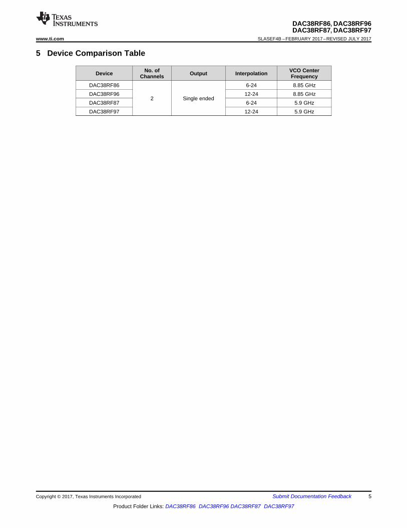
5 Device Comparison Table
Device No. ofChannels Output Interpolation VCO Center
FrequencyDAC38RF86
2 Single ended
6-24 8.85 GHzDAC38RF96 12-24 8.85 GHzDAC38RF87 6-24 5.9 GHzDAC38RF97 12-24 5.9 GHz
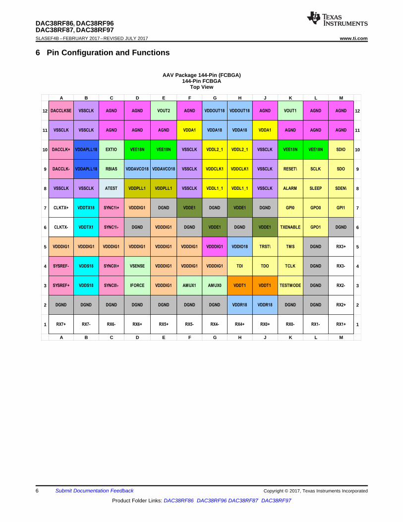
A B C D E F G H J K L M
12 DACCLKSE VSSCLK AGND AGND VOUT2 AGND VDDOUT18 VDDOUT18 AGND VOUT1 AGND AGND 12
11 VSSCLK VSSCLK AGND AGND AGND VDDA1 VDDA18 VDDA18 VDDA1 AGND AGND AGND 11
10 DACCLK+ VDDAPLL18 EXTIO VEE18N VEE18N VSSCLK VDDL2_1 VDDL2_1 VSSCLK VEE18N VEE18N SDIO 10
9 DACCLK- VDDAPLL18 RBIAS VDDAVCO18 VDDAVCO18 VSSCLK VDDCLK1 VDDCLK1 VSSCLK RESET\ SCLK SDO 9
8 VSSCLK VSSCLK ATEST VDDPLL1 VDDPLL1 VSSCLK VDDL1_1 VDDL1_1 VSSCLK ALARM SLEEP SDEN\ 8
7 CLKTX+ VDDTX18 SYNC1\+ VDDDIG1 DGND VDDE1 DGND VDDE1 DGND GPI0 GPO0 GPI1 7
6 CLKTX- VDDTX1 SYNC1\- DGND VDDDIG1 DGND VDDE1 DGND VDDE1 TXENABLE GPO1 DGND 6
5 VDDDIG1 VDDDIG1 VDDDIG1 VDDDIG1 VDDDIG1 VDDDIG1 VDDDIG1 VDDIO18 TRST\ TMS DGND RX3+ 5
4 SYSREF- VDDS18 SYNC0\+ VSENSE VDDDIG1 VDDDIG1 VDDDIG1 TDI TDO TCLK DGND RX3- 4
3 SYSREF+ VDDS18 SYNC0\- IFORCE VDDDIG1 AMUX1 AMUX0 VDDT1 VDDT1 TESTMODE DGND RX2- 3
2 DGND DGND DGND DGND DGND DGND DGND VDDR18 VDDR18 DGND DGND RX2+ 2
1 RX7+ RX7- RX6- RX6+ RX5+ RX5- RX4- RX4+ RX0+ RX0- RX1- RX1+ 1
A B C D E F G H J K L M
6
DAC38RF86, DAC38RF96DAC38RF87, DAC38RF97SLASEF4B –FEBRUARY 2017–REVISED JULY 2017 www.ti.com
Product Folder Links: DAC38RF86 DAC38RF96 DAC38RF87 DAC38RF97
Submit Documentation Feedback Copyright © 2017, Texas Instruments Incorporated
6 Pin Configuration and Functions
AAV Package 144-Pin (FCBGA)144-Pin FCBGA
Top View

7
DAC38RF86, DAC38RF96DAC38RF87, DAC38RF97
www.ti.com SLASEF4B –FEBRUARY 2017–REVISED JULY 2017
Product Folder Links: DAC38RF86 DAC38RF96 DAC38RF87 DAC38RF97
Submit Documentation FeedbackCopyright © 2017, Texas Instruments Incorporated
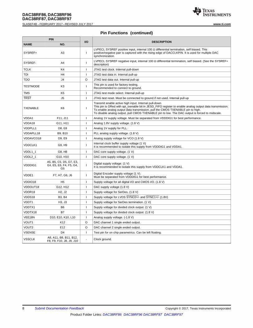
Pin FunctionsPIN
I/O DESCRIPTIONNAME NO.
AGNDC11, C12, D11, E11,F12, J12, K11, L11,M11, M12, D12, L12
- Analog ground.
ALARM K8 O CMOS output for ALARM condition. Default polarity is active low, but can be changed to active high viaRESET_CONFIG alm_out_pol control bit.
AMUX0 G3 O Analog test pin for SerDes, Lane 0 to Lane 3. Can be left floating.
AMUX1 F3 O Analog test pin for SerDes, Lane 4 to Lane 7. Can be left floating.
ATEST C8 O Analog test pin for DAC, references and PLL. Can be left floating.
CLKTX+ A7 O Divided output clock, internal 100 Ω differential termination, self-biased, positive terminal.
CLKTX- A6 O Divided output clock, internal 100 Ω differential termination, self-biased, negative terminal.
DACCLK+ A10 I Device clock, internal 100 Ω differential termination, self-biased, positive terminal.
DACCLK- A9 I Device clock, internal 100 Ω differential termination, self-biased, negative terminal.
DACCLKSE A12 I Single ended device clock optional input. Can be left floating if not used. internal 50 Ω termination.
DGND
A2, B2, C2, D2, D6, E2,E7, F2, F6, G2, G7, H6,J7, K2, L2, L3, L4, L5,
M6
- Digital ground.
EXTIO C10 Requires a 0.1 μF decoupling capacitor to AGND.
GPI0 L6 Factory use only. User should GND.
GPI1 M7 Factory use only. User should GND.
GPO0 L7 Used for CMOS SYNC0\ signal.
GPIO1 K7 Used for CMOS SYNC1\ signal.
IFORCE D3 Test pin for on chip parametrics. Can be left floating.
RBIAS C9 I/O Full-scale output current bias. Change the full-scale output current through DACFS in register DACFS(8.5.72). Expected to be 3.6 kΩ to GND for 40 mA full scale output.
RESET K9 I Active low input for chip RESET, which resets all the programming registers to their default state. Internalpull-up.
RX0+ J1 I CML SerDes interface lane 0 input, positive
RX0- K1 I CML SerDes interface lane 0 input, negative
RX1+ M1 I CML SerDes interface lane 1 input, positive
RX1- L1 I CML SerDes interface lane 1 input, negative
RX2+ M2 I CML SerDes interface lane 2 input, positive
RX2- M3 I CML SerDes interface lane 2 input, negative
RX3+ M5 I CML SerDes interface lane 3 input, positive
RX3- M4 I CML SerDes interface lane 3 input, negative
RX4+ H1 I CML SerDes interface lane 4 input, positive
RX4- G1 I CML SerDes interface lane 4 input, negative
RX5+ E1 I CML SerDes interface lane 5 input, positive
RX5- F1 I CML SerDes interface lane 5 input, negative
RX6+ D1 I CML SerDes interface lane 6 input, positive
RX6- C1 I CML SerDes interface lane 6 input, negative
RX7+ A1 I CML SerDes interface lane 7 input, positive
RX7- B1 I CML SerDes interface lane 7 input, negative
SCLK L9 I Serial interface clock. Internal pull-down.
SDEN M8 I Active low serial data enable, always an input to the DAC38RFxx. Internal pull-up.
SDIO M10 I/O Serial interface data. Bi-directional in 3-pin mode (default) and uni-directional input 4-pin mode. Internalpull-down.
SDO M9 O Uni-directional serial interface data output in 4-pin mode. The SDO pin is tri-stated in 3-pin interfacemode (default).
SLEEP L8 I Active high asynchronous hardware power-down input. Internal pull-down.
SYNC0+ C4 O Synchronization request to transmitter for JESD204B link 0, LVDS positive output.
SYNC0- C3 O Synchronization request to transmitter for JESD204B link 0, LVDS negative output.
SYNC1+ C7 O Synchronization request to transmitter for JESD204B link 1, LVDS positive output.
SYNC1- C6 O Synchronization request to transmitter for JESD204B link 1, LVDS negative output.
8
DAC38RF86, DAC38RF96DAC38RF87, DAC38RF97SLASEF4B –FEBRUARY 2017–REVISED JULY 2017 www.ti.com
Product Folder Links: DAC38RF86 DAC38RF96 DAC38RF87 DAC38RF97
Submit Documentation Feedback Copyright © 2017, Texas Instruments Incorporated
Pin Functions (continued)PIN
I/O DESCRIPTIONNAME NO.
SYSREF+ A3 ILVPECL SYSREF positive input, internal 100 Ω differential termination, self biased. Thispositive/negative pair is captured with the rising edge of DACCLKP/N. It is used for multiple DACsynchronization.
SYSREF- A4 I LVPECL SYSREF negative input, internal 100 Ω differential termination, self biased. (See the SYSREF+description)
TCLK K4 I JTAG test clock. Internal pull-down
TDI H4 I JTAG test data in. Internal pull-up
TDO J4 O JTAG test data out. Internal pull-up
TESTMODE K3 I This pin is used for factory testing.Recommended to connect to ground.
TMS K5 I JTAG test mode select. Internal pull-up
TRST J5 I JTAG test reset. Must be connected to ground if not used. Internal pull-up
TXENABLE K6 I
Transmit enable active high input. Internal pull-down.This pin is ORed with spi_txenable bit in JESD_FIFO register to enable analog output data transmission.To enable analog output data transmission, pull the CMOS TXENABLE pin to high.To disable analog output, pull CMOS TXENABLE pin to low. The DAC output is forced to midscale.
VDDA1 F11, J11 I Analog 1V supply voltage. Must be separated from VDDDIG1 for best performance.
VDDA18 G11, H11 I Analog 1.8V supply voltage. (1.8 V)
VDDPLL1 D8, E8 I Analog 1V supply for PLL.
VDDAPLL18 B9, B10 I PLL analog supply voltage. (1.8 V)
VDDAVCO18 D9, E9 I Analog supply voltage for VCO (1.8 V)
VDDCLK1 G9, H9 I Internal clock buffer supply voltage (1 V)It is recommended to isolate this supply from VDDDIG1 and VDDA1.
VDDL1_1 G8, H8 I DAC core supply voltage. (1 V)
VDDL2_1 G10, H10 I DAC core supply voltage. (1 V)
VDDDIG1A5, B5, C5, D5, D7, E3,E4, E5, E6, F4, F5, G4,
G5I Digital supply voltage. (1 V)
It is recommended to isolate this supply from VDDCLK1 and VDDA1.
VDDE1 F7, H7, G6, J6 I Digital Encoder supply voltage (1 V).Must be separated from VDDDIG1 for best performance.
VDDIO18 H5 I Supply voltage for all digital I/O and CMOS I/O. (1.8 V)
VDDOUT18 G12, H12 I DAC supply voltage (1.8 V)
VDDR18 H2, J2 I Supply voltage for SerDes. (1.8 V)
VDDS18 B3, B4 I Supply voltage for LVDS SYNC0+/- and SYNC1+/- (1.8V)
VDDT1 H3, J3 I Supply voltage for SerDes termination. (1 V)
VDDTX1 B6 I Supply voltage for divided clock output. (1 V)
VDDTX18 B7 I Supply voltage for divided clock output. (1.8 V)
VEE18N D10, E10, K10, L10 I Analog supply voltage. (-1.8 V)
VOUT1 K12 O DAC channel 1 single ended output.
VOUT2 E12 O DAC channel 2 single ended output.
VSENSE D4 I Test pin for on chip parametrics. Can be left floating.
VSSCLK A8, A11, B8, B11, B12,F8, F9, F10, J8, J9, J10 - Clock ground.
9
DAC38RF86, DAC38RF96DAC38RF87, DAC38RF97
www.ti.com SLASEF4B –FEBRUARY 2017–REVISED JULY 2017
Product Folder Links: DAC38RF86 DAC38RF96 DAC38RF87 DAC38RF97
Submit Documentation FeedbackCopyright © 2017, Texas Instruments Incorporated
(1) Stresses beyond those listed under Absolute Maximum Ratings may cause permanent damage to the device. These are stress ratingsonly, which do not imply functional operation of the device at these or any other conditions beyond those indicated under RecommendedOperating Conditions. Exposure to absolute-maximum-rated conditions for extended periods may affect device reliability.
(2) Measured with respect to AGND or DGND.
7 Specifications
7.1 Absolute Maximum Ratingsover operating free-air temperature range (unless otherwise noted) (1)
MIN MAX UNIT
Supply Voltage Range (2)
VDDDAC1, VDDDIG1, VDDL1_1, VDDL2_1,VDDCLK1, VDDT1, VDDCLK1, VDDTX1, VDDE1 –0.3 1.3 V
VDDR18, VDDIO18, VDDS18, VDDAPLL18,VDDOUT18, VDDA18, VDDAVCO18, VDDTX18 –0.3 2.45 V
VEE18N –2 0.3 V
Voltage between AGND and DGND –0.3 0.3 V
Pin Voltage Range (2)
RX[0..7]+/- –0.5 VDDDIG1 + 0.5 V V
SDEN, SCLK, SDIO, SDO, TXENABLE, ALARM,RESET, SLEEP, TMS, TCLK, TDI, TDO, TRST,TESTMODE, GPI0, GPI1, GPO0, GPO1
–0.5 VDDIO + 0.5 V V
CLKOUT+/- –0.5 VDDTX18 + 0.5 V V
DACCLK+/-, SYSREF+/-, DACCLKSE –0.5 VDDCLK1 + 0.5 V V
SYNC0+/-, SYNC1+/- –0.5 VDDS18 + 0.5 V V
VOUT1+/-, VOUT2+/- –0.5 VDDAOUT18 + 0.5 V V
RBIAS, EXTIO, ATEST –0.5 VDDAOUT18 + 0.5 V V
IFORCE, VSENSE –0.5 VDDDIG1 + 0.5 V V
AMUX1, AMUX0 –0.5 VDDT1 + 0.5 V V
Peak input current (any input) 20 mA
Peak total input current (all inputs) –30 mA
Junction temperature TJ 150 °C
Operating free-air temperature, TA –40 85 °C
Storage temperature, Tstg –65 150 °C
(1) JEDEC document JEP155 states that 500-V HBM allows safe manufacturing with a standard ESD control process.(2) JEDEC document JEP157 states that 250-V CDM allows safe manufacturing with a standard ESD control process.
7.2 ESD RatingsVALUE UNIT
V(ESD) Electrostatic dischargeHuman-body model (HBM), per ANSI/ESDA/JEDEC JS-001 (1) ±1000
VCharged-device model (CDM), per JEDEC specification JESD22-C101 (2) ±250
(1) Prolonged use at this junction temperature may increase the device failure-in-time (FIT) rate
7.3 Recommended Operating Conditionsover operating free-air temperature range (unless otherwise noted)
MIN NOM MAX UNIT
TJRecommended operating temperature 105 °C
Maximum rated operating junction temperature (1) 125 °C
TA Recommended free-air temperature –40 85 °C
Supply Voltage Range
VDDA18, VDDAPLL18, VDDS18, VDDIO18, VDDR18,VDDAPLL18, VDDOUT18, VDDAVCO18 1.71 1.8 1.89 V
VDDDIG1 VDDA1, VDDT1, VDDAPLL1, VDDCLK1, VDDL1_1,VDDL2_1, VDDTX1, VDDE1 0.95 1 1.05 V
VEE18N -1.89 -1.8 -1.71 V
10
DAC38RF86, DAC38RF96DAC38RF87, DAC38RF97SLASEF4B –FEBRUARY 2017–REVISED JULY 2017 www.ti.com
Product Folder Links: DAC38RF86 DAC38RF96 DAC38RF87 DAC38RF97
Submit Documentation Feedback Copyright © 2017, Texas Instruments Incorporated
(1) For more information about traditional and new thermal metrics, see the Semiconductor and IC Package Thermal Metrics applicationreport.
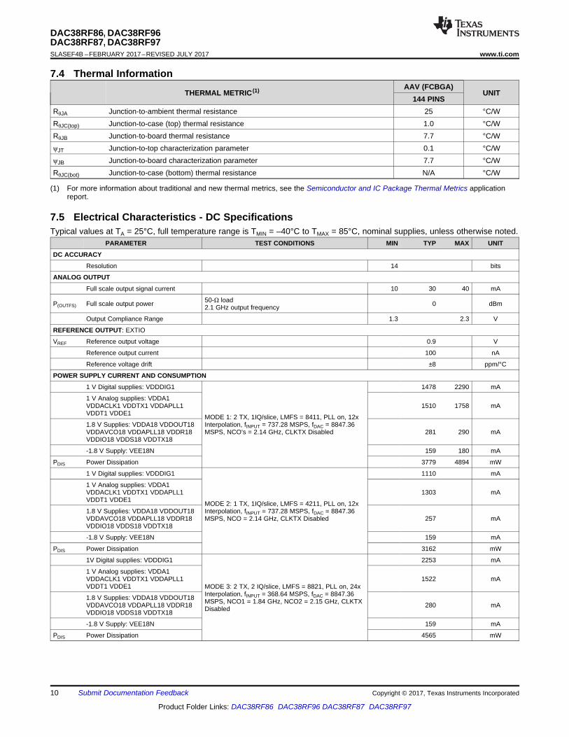
7.4 Thermal Information
THERMAL METRIC (1) AAV (FCBGA)UNIT
144 PINSRθJA Junction-to-ambient thermal resistance 25 °C/WRθJC(top) Junction-to-case (top) thermal resistance 1.0 °C/WRθJB Junction-to-board thermal resistance 7.7 °C/WψJT Junction-to-top characterization parameter 0.1 °C/WψJB Junction-to-board characterization parameter 7.7 °C/WRθJC(bot) Junction-to-case (bottom) thermal resistance N/A °C/W
7.5 Electrical Characteristics - DC SpecificationsTypical values at TA = 25°C, full temperature range is TMIN = –40°C to TMAX = 85°C, nominal supplies, unless otherwise noted.
PARAMETER TEST CONDITIONS MIN TYP MAX UNIT
DC ACCURACY
Resolution 14 bits
ANALOG OUTPUT
Full scale output signal current 10 30 40 mA
P(OUTFS) Full scale output power 50-Ω load2.1 GHz output frequency 0 dBm
Output Compliance Range 1.3 2.3 V
REFERENCE OUTPUT: EXTIO
VREF Reference output voltage 0.9 V
Reference output current 100 nA
Reference voltage drift ±8 ppm/°C
POWER SUPPLY CURRENT AND CONSUMPTION
1 V Digital supplies: VDDDIG1
MODE 1: 2 TX, 1IQ/slice, LMFS = 8411, PLL on, 12xInterpolation, fINPUT = 737.28 MSPS, fDAC = 8847.36MSPS, NCO’s = 2.14 GHz, CLKTX Disabled
1478 2290 mA
1 V Analog supplies: VDDA1VDDACLK1 VDDTX1 VDDAPLL1VDDT1 VDDE1
1510 1758 mA
1.8 V Supplies: VDDA18 VDDOUT18VDDAVCO18 VDDAPLL18 VDDR18VDDIO18 VDDS18 VDDTX18
281 290 mA
-1.8 V Supply: VEE18N 159 180 mA
PDIS Power Dissipation 3779 4894 mW
1 V Digital supplies: VDDDIG1
MODE 2: 1 TX, 1IQ/slice, LMFS = 4211, PLL on, 12xInterpolation, fINPUT = 737.28 MSPS, fDAC = 8847.36MSPS, NCO = 2.14 GHz, CLKTX Disabled
1110 mA
1 V Analog supplies: VDDA1VDDACLK1 VDDTX1 VDDAPLL1VDDT1 VDDE1
1303 mA
1.8 V Supplies: VDDA18 VDDOUT18VDDAVCO18 VDDAPLL18 VDDR18VDDIO18 VDDS18 VDDTX18
257 mA
-1.8 V Supply: VEE18N 159 mA
PDIS Power Dissipation 3162 mW
1V Digital supplies: VDDDIG1
MODE 3: 2 TX, 2 IQ/slice, LMFS = 8821, PLL on, 24xInterpolation, fINPUT = 368.64 MSPS, fDAC = 8847.36MSPS, NCO1 = 1.84 GHz, NCO2 = 2.15 GHz, CLKTXDisabled
2253 mA
1 V Analog supplies: VDDA1VDDACLK1 VDDTX1 VDDAPLL1VDDT1 VDDE1
1522 mA
1.8 V Supplies: VDDA18 VDDOUT18VDDAVCO18 VDDAPLL18 VDDR18VDDIO18 VDDS18 VDDTX18
280 mA
-1.8 V Supply: VEE18N 159 mA
PDIS Power Dissipation 4565 mW

11
DAC38RF86, DAC38RF96DAC38RF87, DAC38RF97
www.ti.com SLASEF4B –FEBRUARY 2017–REVISED JULY 2017
Product Folder Links: DAC38RF86 DAC38RF96 DAC38RF87 DAC38RF97
Submit Documentation FeedbackCopyright © 2017, Texas Instruments Incorporated
Electrical Characteristics - DC Specifications (continued)Typical values at TA = 25°C, full temperature range is TMIN = –40°C to TMAX = 85°C, nominal supplies, unless otherwise noted.
PARAMETER TEST CONDITIONS MIN TYP MAX UNIT
1 V Digital supplies: VDDDIG1
MODE 4: 1 TX, 2 IQ/slice, LMFS = 4421, PLL on, 24xInterpolation, fINPUT = 368.64 MSPS, fDAC = 8847.36MSPS, NCO1 = 1.84 GHz, NCO2 = 2.15 GHz, CLKTXDisabled
1701 mA
1 V Analog supplies: VDDA1VDDACLK1 VDDTX1 VDDAPLL1VDDT1 VDDE1
1314 mA
1.8 V Supplies: VDDA18 VDDOUT18VDDAVCO18 VDDAPLL18 VDDR18VDDIO18 VDDS18 VDDTX18
256 mA
-1.8 V Supply: VEE18N 159 mA
PDIS Power Dissipation 3763 mW
1 V Digital supplies: VDDDIG1
MODE 5: 2 TX, 1 IQ/slice, LMFS = 4421, PLL on, 18xInterpolation, fINPUT = 491.52 MSPS, fDAC = 8847.36MSPS, NCO1 = 2.14 GHz, CLKTX Disabled
1328 mA
1 V Analog supplies: VDDA1VDDACLK1 VDDTX1 VDDAPLL1VDDT1 VDDE1
1312 mA
1.8 V Supplies: VDDA18 VDDOUT18VDDAVCO18 VDDAPLL18 VDDR18VDDIO18 VDDS18 VDDTX18
249 mA
-1.8 V Supply: VEE18N 159 mA
PDIS Power Dissipation 3374 mW
1 V Digital supplies: VDDDIG1
MODE 6: 1 TX, 1 IQ/slice, LMFS = 2221, PLL on, 18xInterpolation, fINPUT = 491.52 MSPS, fDAC = 8847.36MSPS, NCO1 = 2.14 GHz, CLKTX Disabled
1027 mA
1 V Analog supplies: VDDA1VDDACLK1 VDDTX1 VDDAPLL1VDDT1 VDDE1
1206 mA
1.8 V Supplies: VDDA18 VDDOUT18VDDAVCO18 VDDAPLL18 VDDR18VDDIO18 VDDS18 VDDTX18
248 mA
-1.8 V Supply: VEE18N 159 mA
PDIS Power Dissipation 2964 mW
1 V Digital supplies: VDDDIG1
MODE 7: 2 TX, 1 IQ/slice, LMFS = 8411, PLL on, 6xInterpolation, fINPUT = 983.04 MSPS, fDAC = 5898.24MSPS, NCO1 = 2.14 GHz, CLKTX Disabled
1157 mA
1 V Analog supplies: VDDA1VDDACLK1 VDDTX1 VDDAPLL1VDDT1 VDDE1
1125 mA
1.8 V Supplies: VDDA18 VDDOUT18VDDAVCO18 VDDAPLL18 VDDR18VDDIO18 VDDS18 VDDTX18
246 mA
-1.8 V Supply: VEE18N 159 mA
PDIS Power Dissipation 3011 mW
1 V Digital supplies: VDDDIG1
MODE 8: 1 TX, 1 IQ/slice, LMFS = 4211, PLL on, 6xInterpolation, fINPUT = 983.04 MSPS, fDAC = 5898.24MSPS, NCO1 = 2.14 GHz, CLKTX Disabled
848 mA
1 V Analog supplies: VDDA1VDDACLK1 VDDTX1 VDDAPLL1VDDT1 VDDE1
647 mA
1.8 V Supplies: VDDA18 VDDOUT18VDDAVCO18 VDDAPLL18 VDDR18VDDIO18 VDDS18 VDDTX18
230 mA
-1.8 V Supply: VEE18N 159 mA
PDIS Power Dissipation 2195 mW
1 V Digital supplies: VDDDIG1
MODE 9: 2 TX, 2 IQ/slice, LMFS = 4831, PLL on, 24xInterpolation, fINPUT = 368.64 MSPS, fDAC = 8847.36MSPS, NCO1 = 2.14 GHz, CLKTX Disabled
2131 mA
1 V Analog supplies: VDDA1VDDACLK1 VDDTX1 VDDAPLL1VDDT1 VDDE1
1324 mA
1.8 V Supplies: VDDA18 VDDOUT18VDDAVCO18 VDDAPLL18 VDDR18VDDIO18 VDDS18 VDDTX18
251 mA
-1.8 V Supply: VEE18N 159 mA
PDIS Power Dissipation 4192 mW

12
DAC38RF86, DAC38RF96DAC38RF87, DAC38RF97SLASEF4B –FEBRUARY 2017–REVISED JULY 2017 www.ti.com
Product Folder Links: DAC38RF86 DAC38RF96 DAC38RF87 DAC38RF97
Submit Documentation Feedback Copyright © 2017, Texas Instruments Incorporated
Electrical Characteristics - DC Specifications (continued)Typical values at TA = 25°C, full temperature range is TMIN = –40°C to TMAX = 85°C, nominal supplies, unless otherwise noted.
PARAMETER TEST CONDITIONS MIN TYP MAX UNIT
1 V Digital supplies: VDDDIG1
MODE 10: 1 TX, 2 IQ/slice, LMFS = 2431, PLL on, 24xInterpolation, fINPUT = 368.64 MSPS, fDAC = 8847.36MSPS, NCO1 = 2.14 GHz, CLKTX Disabled
1635 mA
1 V Analog supplies: VDDA1VDDACLK1 VDDTX1 VDDAPLL1VDDT1 VDDE1
1212 mA
1.8 V Supplies: VDDA18 VDDOUT18VDDAVCO18 VDDAPLL18 VDDR18VDDIO18 VDDS18 VDDTX18
250 mA
-1.8 V Supply: VEE18N 159 mA
PDIS Power Dissipation 3583 mW
1 V Digital supplies: VDDDIG1
MODE 11: Power down mode, no clock, DACs insleep, SerDes in sleep
63 568 mA
1 V Analog supplies: VDDA1VDDACLK1 VDDTX1 VDDAPLL1VDDT1 VDDE1
18 105 mA
1.8 V Supplies: VDDA18 VDDOUT18VDDAVCO18 VDDAPLL18 VDDR18VDDIO18 VDDS18 VDDTX18
47 51 mA
-1.8 V Supply: VEE18N 23 28 mA
PDIS Power Dissipation 208 815 mW
VDDTX1fDAC = 8847 MSPS, Clock Out Divider Enabled 25 mA
fDAC = 5898 MSPS, Clock Out Divider Enabled 19 mA
VDDTX18 Clock Out Enabled 16 mA
13
DAC38RF86, DAC38RF96DAC38RF87, DAC38RF97
www.ti.com SLASEF4B –FEBRUARY 2017–REVISED JULY 2017
Product Folder Links: DAC38RF86 DAC38RF96 DAC38RF87 DAC38RF97
Submit Documentation FeedbackCopyright © 2017, Texas Instruments Incorporated
7.6 Electrical Characteristics - Digital SpecificationsTypical values at TA = 25°C, full temperature range is TMIN = –40°C to TMAX = 85°C, nominal supplies, unless otherwise noted.
PARAMETER TEST CONDITIONS MIN TYP MAX UNIT
CML SerDes INPUTS: RX[7:0]+/-
VDIFF Receiver input amplitude 50 1200 mV
VCOM Input common mode voltage
TERM = 111 600
mVTERM = 001 700
TERM = 100 0
TERM = 101 250
ZDDIFF Internal differential termination 85 100 115 Ω
fSerDes SerDes bit rate 0.78125 12.5 Gbps
DIFFERENTIAL CLOCK INPUTS: SYSREF+/-, DACCLK+/-
fDACCLK DACCLK input frequency 0.1 9 GHz
VCOM Differential input common mode voltage 0.5 V
VI(DPP) Differential input peak-to-peak voltage 800 2000 mV
ZT Internal termination 100 Ω
CL Input capacitance 2 pF
Duty cycle (DACCLK only) 40% 60%
LVDS OUTPUT: SYNC0+/-, SYNC1+/-
VCOM Output common mode voltage 1.2 V
ZT Internal termination 100 Ω
VOD Differential output voltage swing 500 mV
CML OUTPUT: CLKTX+/-
VOD CML OUTPUT: CLKTX+/- 1300 mV
CMOS INTERFACE: SDEN, SCLK, SDIO, SDO, TXENABLE, ALARM, RESET, SLEEP, TMS, TCLK, TDI, TDO, TRST, TESTMODE, SYNCSE1,SYNCSE2
VIH High-level input voltage 0.7 x VDDIO V
VIL Low-level input voltage 0.3 x VDDIO V
IIH High-level input current –40 40 µA
IIL Low-level input current –40 40 µA
CI CMOS input capacitance 2 pF
VOH High-level output voltageILOAD = –100 µA VDDIO – 0.2
VILOAD = –2 mA 0.8 x VDDIO
VOL Low-level output voltageILOAD = 100 µA 0.2
VILOAD = 2 mA 0.5
LATENCY
RX SerDes Digital Delay
full rate, RATE = “00” 34
UIhalf rate, RATE = “01” 29
quarter rate, RATE = “10” 26.5
eighth rate, RATE = “11” 26.25
SerDes output to JED204B elastic bufferinput latency 21 - 39
JESDclockcycles
14
DAC38RF86, DAC38RF96DAC38RF87, DAC38RF97SLASEF4B –FEBRUARY 2017–REVISED JULY 2017 www.ti.com
Product Folder Links: DAC38RF86 DAC38RF96 DAC38RF87 DAC38RF97
Submit Documentation Feedback Copyright © 2017, Texas Instruments Incorporated
Electrical Characteristics - Digital Specifications (continued)Typical values at TA = 25°C, full temperature range is TMIN = –40°C to TMAX = 85°C, nominal supplies, unless otherwise noted.
PARAMETER TEST CONDITIONS MIN TYP MAX UNIT
Digital Latency: JESD Buffer to DAC Output
LMFSHD = 82121, 6x Interpolation 856
DACclockcycles
LMFSHD = 82121, 8x Interpolation 1120
LMFSHD = 82121, 12x Interpolation 1602
LMFSHD = 82121, 16x Interpolation 2091
LMFSHD = 42111 or 84111, 6xInterpolation 817
LMFSHD = 42111 or 84111, 8xInterpolation 1057
LMFSHD = 42111 or 84111, 10xInterpolation 1184
LMFSHD = 42111 or 84111, 12xInterpolation 1532
LMFSHD = 42111 or 84111, 16xInterpolation 1997
LMFSHD = 42111 or 84111, 18xInterpolation 2142
LMFSHD = 42111 or 84111, 24xInterpolation 2941
LMFSHD = 22210 or 44210, 8xInterpolation 1020
LMFSHD = 22210 or 44210, 12xInterpolation 1473
LMFSHD = 22210 or 44210, 16xInterpolation 1917
LMFSHD = 22210 or 44210, 18xInterpolation 2050
LMFSHD = 22210 or 44210, 20xInterpolation 2275
LMFSHD = 22210 or 44210, 24xInterpolation 2821
LMFSHD = 12410 or 24410, 16xInterpolation 1912
LMFSHD = 12410 or 24410, 24xInterpolation 2786
LMFSHD = 44210 or 88210, 8xInterpolation 916
LMFSHD = 44210 or 88210, 12xInterpolation 1317
LMFSHD = 44210 or 88210, 16xInterpolation 1709
LMFSHD = 44210 or 88210, 24xInterpolation 2509
LMFSHD = 24410 or 48410, 16xInterpolation 1672
LMFSHD = 24410 or 48410, 24xInterpolation 1593
15
DAC38RF86, DAC38RF96DAC38RF87, DAC38RF97
www.ti.com SLASEF4B –FEBRUARY 2017–REVISED JULY 2017
Product Folder Links: DAC38RF86 DAC38RF96 DAC38RF87 DAC38RF97
Submit Documentation FeedbackCopyright © 2017, Texas Instruments Incorporated
Electrical Characteristics - Digital Specifications (continued)Typical values at TA = 25°C, full temperature range is TMIN = –40°C to TMAX = 85°C, nominal supplies, unless otherwise noted.
PARAMETER TEST CONDITIONS MIN TYP MAX UNIT
SYSREF TO JESD LMFC RESET
LMFSHD = 82121, 6x Interpolation 5
JESDclockcycles
LMFSHD = 82121, 8x Interpolation 5
LMFSHD = 82121, 12x Interpolation 5
LMFSHD = 82121, 16x Interpolation 5
LMFSHD = 42111 or 84111, 6xInterpolation 16
LMFSHD = 42111 or 84111, 8xInterpolation 16
LMFSHD = 42111 or 84111, 10xInterpolation 15
LMFSHD = 42111 or 84111, 12xInterpolation 15
LMFSHD = 42111 or 84111, 16xInterpolation 13
LMFSHD = 42111 or 84111, 18xInterpolation 15
LMFSHD = 42111 or 84111, 24xInterpolation 15
LMFSHD = 22210 or 44210, 8xInterpolation 8
LMFSHD = 22210 or 44210, 12xInterpolation 7
LMFSHD = 22210 or 44210, 16xInterpolation 6
LMFSHD = 22210 or 44210, 18xInterpolation 7
LMFSHD = 22210 or 44210, 20xInterpolation 5
LMFSHD = 22210 or 44210, 24xInterpolation 4
LMFSHD = 12410 or 24410, 16xInterpolation 9
LMFSHD = 12410 or 24410, 24xInterpolation 7
LMFSHD = 44210 or 88210, 8xInterpolation 29
LMFSHD = 44210 or 88210, 12xInterpolation 27
LMFSHD = 44210 or 88210, 16xInterpolation 26
LMFSHD = 44210 or 88210, 24xInterpolation 25
LMFSHD = 24410 or 48410, 16xInterpolation 8
LMFSHD = 24410 or 48410, 24xInterpolation 6
16
DAC38RF86, DAC38RF96DAC38RF87, DAC38RF97SLASEF4B –FEBRUARY 2017–REVISED JULY 2017 www.ti.com
Product Folder Links: DAC38RF86 DAC38RF96 DAC38RF87 DAC38RF97
Submit Documentation Feedback Copyright © 2017, Texas Instruments Incorporated
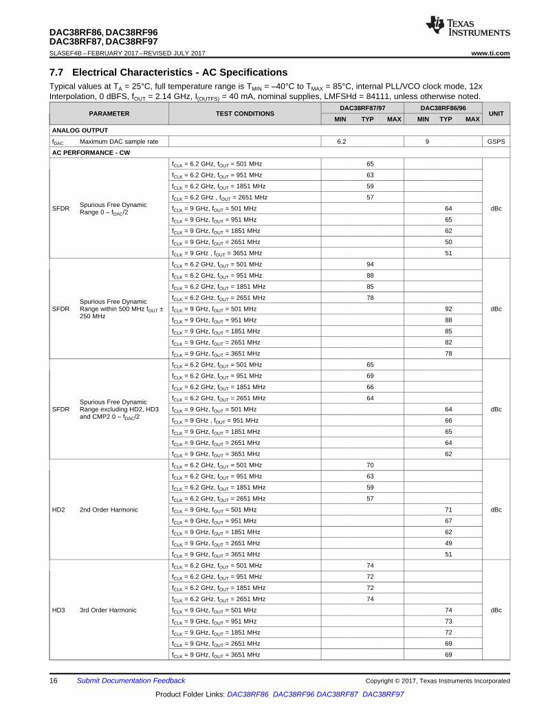
7.7 Electrical Characteristics - AC SpecificationsTypical values at TA = 25°C, full temperature range is TMIN = –40°C to TMAX = 85°C, internal PLL/VCO clock mode, 12xInterpolation, 0 dBFS, fOUT = 2.14 GHz, I(OUTFS) = 40 mA, nominal supplies, LMFSHd = 84111, unless otherwise noted.
PARAMETER TEST CONDITIONSDAC38RF87/97 DAC38RF86/96
UNITMIN TYP MAX MIN TYP MAX
ANALOG OUTPUT
fDAC Maximum DAC sample rate 6.2 9 GSPS
AC PERFORMANCE - CW
SFDR Spurious Free DynamicRange 0 – fDAC/2
fCLK = 6.2 GHz, fOUT = 501 MHz 65
dBc
fCLK = 6.2 GHz, fOUT = 951 MHz 63
fCLK = 6.2 GHz, fOUT = 1851 MHz 59
fCLK = 6.2 GHz , fOUT = 2651 MHz 57
fCLK = 9 GHz, fOUT = 501 MHz 64
fCLK = 9 GHz, fOUT = 951 MHz 65
fCLK = 9 GHz, fOUT = 1851 MHz 62
fCLK = 9 GHz, fOUT = 2651 MHz 50
fCLK = 9 GHz , fOUT = 3651 MHz 51
SFDRSpurious Free DynamicRange within 500 MHz fOUT ±250 MHz
fCLK = 6.2 GHz, fOUT = 501 MHz 94
dBc
fCLK = 6.2 GHz, fOUT = 951 MHz 88
fCLK = 6.2 GHz, fOUT = 1851 MHz 85
fCLK = 6.2 GHz, fOUT = 2651 MHz 78
fCLK = 9 GHz, fOUT = 501 MHz 92
fCLK = 9 GHz, fOUT = 951 MHz 88
fCLK = 9 GHz, fOUT = 1851 MHz 85
fCLK = 9 GHz, fOUT = 2651 MHz 82
fCLK = 9 GHz, fOUT = 3651 MHz 78
SFDRSpurious Free DynamicRange excluding HD2, HD3and CMP2 0 – fDAC/2
fCLK = 6.2 GHz, fOUT = 501 MHz 65
dBc
fCLK = 6.2 GHz, fOUT = 951 MHz 69
fCLK = 6.2 GHz, fOUT = 1851 MHz 66
fCLK = 6.2 GHz, fOUT = 2651 MHz 64
fCLK = 9 GHz, fOUT = 501 MHz 64
fCLK = 9 GHz , fOUT = 951 MHz 66
fCLK = 9 GHz, fOUT = 1851 MHz 65
fCLK = 9 GHz, fOUT = 2651 MHz 64
fCLK = 9 GHz, fOUT = 3651 MHz 62
HD2 2nd Order Harmonic
fCLK = 6.2 GHz, fOUT = 501 MHz 70
dBc
fCLK = 6.2 GHz, fOUT = 951 MHz 63
fCLK = 6.2 GHz, fOUT = 1851 MHz 59
fCLK = 6.2 GHz, fOUT = 2651 MHz 57
fCLK = 9 GHz, fOUT = 501 MHz 71
fCLK = 9 GHz, fOUT = 951 MHz 67
fCLK = 9 GHz, fOUT = 1851 MHz 62
fCLK = 9 GHz, fOUT = 2651 MHz 49
fCLK = 9 GHz, fOUT = 3651 MHz 51
HD3 3rd Order Harmonic
fCLK = 6.2 GHz, fOUT = 501 MHz 74
dBc
fCLK = 6.2 GHz, fOUT = 951 MHz 72
fCLK = 6.2 GHz, fOUT = 1851 MHz 72
fCLK = 6.2 GHz, fOUT = 2651 MHz 74
fCLK = 9 GHz, fOUT = 501 MHz 74
fCLK = 9 GHz, fOUT = 951 MHz 73
fCLK = 9 GHz, fOUT = 1851 MHz 72
fCLK = 9 GHz, fOUT = 2651 MHz 69
fCLK = 9 GHz, fOUT = 3651 MHz 69
17
DAC38RF86, DAC38RF96DAC38RF87, DAC38RF97
www.ti.com SLASEF4B –FEBRUARY 2017–REVISED JULY 2017
Product Folder Links: DAC38RF86 DAC38RF96 DAC38RF87 DAC38RF97
Submit Documentation FeedbackCopyright © 2017, Texas Instruments Incorporated
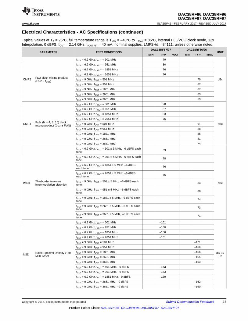
Electrical Characteristics - AC Specifications (continued)Typical values at TA = 25°C, full temperature range is TMIN = –40°C to TMAX = 85°C, internal PLL/VCO clock mode, 12xInterpolation, 0 dBFS, fOUT = 2.14 GHz, I(OUTFS) = 40 mA, nominal supplies, LMFSHd = 84111, unless otherwise noted.
PARAMETER TEST CONDITIONSDAC38RF87/97 DAC38RF86/96
UNITMIN TYP MAX MIN TYP MAX
CMP2 Fs/2 clock mixing product(Fs/2 – fOUT)
fCLK = 6.2 GHz, fOUT = 501 MHz 79
dBc
fCLK = 6.2 GHz, fOUT = 951 MHz 80
fCLK = 6.2 GHz, fOUT = 1851 MHz 76
fCLK = 6.2 GHz, fOUT = 2651 MHz 76
fCLK = 9 GHz, fOUT = 501 MHz 70
fCLK = 9 GHz, fOUT = 951 MHz 67
fCLK = 9 GHz, fOUT = 1851 MHz 67
fCLK = 9 GHz, fOUT = 2651 MHz 63
fCLK = 9 GHz, fOUT = 3651 MHz 59
CMP4+ Fs/N (N = 4, 8, 16) clockmixing product (fOUT ± Fs/N)
fCLK = 6.2 GHz, fOUT = 501 MHz 90
dBc
fCLK = 6.2 GHz, fOUT = 951 MHz 87
fCLK = 6.2 GHz, fOUT = 1851 MHz 83
fCLK = 6.2 GHz, fOUT = 2651 MHz 76
fCLK = 9 GHz, fOUT = 501 MHz 91
fCLK = 9 GHz, fOUT = 951 MHz 88
fCLK = 9 GHz, fOUT = 1851 MHz 85
fCLK = 9 GHz, fOUT = 2651 MHz 81
fCLK = 9 GHz, fOUT = 3651 MHz 74
IMD3 Third-order two-toneintermodulation distortion
fCLK = 6.2 GHz, fOUT = 501 ± 5 MHz, –6 dBFS eachtone 83
dBc
fCLK = 6.2 GHz, fOUT = 951 ± 5 MHz, –6 dBFS eachtone 78
fCLK = 6.2 GHz, fOUT = 1851 ± 5 MHz, –6 dBFSeach tone 76
fCLK = 6.2 GHz, fOUT = 2651 ± 5 MHz, –6 dBFSeach tone 76
fCLK = 9 GHz, fOUT = 501 ± 5 MHz, –6 dBFS eachtone 84
fCLK = 9 GHz, fOUT = 951 ± 5 MHz, –6 dBFS eachtone 80
fCLK = 9 GHz, fOUT = 1851 ± 5 MHz, –6 dBFS eachtone 74
fCLK = 9 GHz, fOUT = 2651 ± 5 MHz, –6 dBFS eachtone 73
fCLK = 9 GHz, fOUT = 3651 ± 5 MHz, –6 dBFS eachtone 71
NSD Noise Spectral Density > 50MHz offset
fCLK = 6.2 GHz, fOUT = 501 MHz –161
dBFS/Hz
fCLK = 6.2 GHz, fOUT = 951 MHz –160
fCLK = 6.2 GHz, fOUT = 1851 MHz –156
fCLK = 6.2 GHz, fOUT = 2651 MHz –151
fCLK = 9 GHz, fOUT = 501 MHz –171
fCLK = 9 GHz, fOUT = 951 MHz –166
fCLK = 9 GHz, fOUT = 1851 MHz –156
fCLK = 9 GHz, fOUT = 2651 MHz –155
fCLK = 9 GHz, fOUT = 3651 MHz –153
fCLK = 6.2 GHz, fOUT = 501 MHz, –9 dBFS –163
fCLK = 6.2 GHz, fOUT = 951 MHz, –9 dBFS –163
fCLK = 6.2 GHz, fOUT = 1851 MHz, –9 dBFS –160
fCLK = 9 GHz, fOUT = 2651 MHz, –9 dBFS –162
fCLK = 9 GHz, fOUT = 3651 MHz, –9 dBFS –160

18
DAC38RF86, DAC38RF96DAC38RF87, DAC38RF97SLASEF4B –FEBRUARY 2017–REVISED JULY 2017 www.ti.com
Product Folder Links: DAC38RF86 DAC38RF96 DAC38RF87 DAC38RF97
Submit Documentation Feedback Copyright © 2017, Texas Instruments Incorporated
Electrical Characteristics - AC Specifications (continued)Typical values at TA = 25°C, full temperature range is TMIN = –40°C to TMAX = 85°C, internal PLL/VCO clock mode, 12xInterpolation, 0 dBFS, fOUT = 2.14 GHz, I(OUTFS) = 40 mA, nominal supplies, LMFSHd = 84111, unless otherwise noted.
PARAMETER TEST CONDITIONSDAC38RF87/97 DAC38RF86/96
UNITMIN TYP MAX MIN TYP MAX
Isolation
Isolation between DAC A andDAC B analog output
fOUT = 1856 MHz 60 60dBc
fOUT = 3105 MHz 55 55
AC PERFORMANCE – Modulated Signals
ACPR WCDMA 1 carrier adjacentchannel power ratio
fCLK = 5898.24 MHz, fOUT = 950 MHz 77
dBcfCLK = 5898.24 MHz, fOUT = 2140 MHz 73
fCLK = 8847.36 MHz , fOUT = 950 MHz 75
fCLK = 8847.36 MHz, fOUT = 2140 MHz 69
Alt-ACLR
WCDMA 1 carrier alternatechannel ACPR
fCLK = 5898.24 MHz , fOUT = 950 MHz 82
dBcfCLK = 5898.24 MHz, fOUT = 2140 MHz 78
fCLK = 8847.36 MHz , fOUT = 950 MHz 81
fCLK = 8847.36 MHz, fOUT = 2140 MHz 77
LTE20 20 MHz LTE adjacent channelpower ratio
fCLK = 5898.24 MHz, fOUT = 800 MHz 75
dBc
fCLK = 5898.24 MHz, fOUT = 2650 MHz 69
fCLK = 8847.36 MHz , fOUT = 800 MHz 73
fCLK = 8847.36 MHz, fOUT = 2650 MHz 67
fCLK = 8847.36 MHz, fOUT = 3700 MHz 64
19
DAC38RF86, DAC38RF96DAC38RF87, DAC38RF97
www.ti.com SLASEF4B –FEBRUARY 2017–REVISED JULY 2017
Product Folder Links: DAC38RF86 DAC38RF96 DAC38RF87 DAC38RF97
Submit Documentation FeedbackCopyright © 2017, Texas Instruments Incorporated
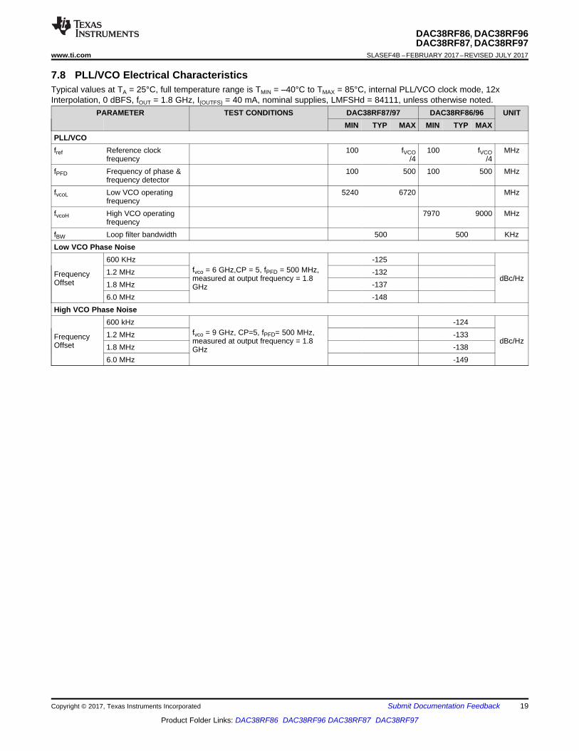
7.8 PLL/VCO Electrical CharacteristicsTypical values at TA = 25°C, full temperature range is TMIN = –40°C to TMAX = 85°C, internal PLL/VCO clock mode, 12xInterpolation, 0 dBFS, fOUT = 1.8 GHz, I(OUTFS) = 40 mA, nominal supplies, LMFSHd = 84111, unless otherwise noted.
PARAMETER TEST CONDITIONS DAC38RF87/97 DAC38RF86/96 UNITMIN TYP MAX MIN TYP MAX
PLL/VCOfref Reference clock
frequency100 fVCO
/4100 fVCO
/4MHz
fPFD Frequency of phase &frequency detector
100 500 100 500 MHz
fvcoL Low VCO operatingfrequency
5240 6720 MHz
fvcoH High VCO operatingfrequency
7970 9000 MHz
fBW Loop filter bandwidth 500 500 KHzLow VCO Phase Noise
FrequencyOffset
600 KHzfvco = 6 GHz,CP = 5, fPFD = 500 MHz,measured at output frequency = 1.8GHz
-125
dBc/Hz1.2 MHz -1321.8 MHz -1376.0 MHz -148
High VCO Phase Noise
FrequencyOffset
600 kHzfvco = 9 GHz, CP=5, fPFD= 500 MHz,measured at output frequency = 1.8GHz
-124
dBc/Hz1.2 MHz -1331.8 MHz -1386.0 MHz -149
20
DAC38RF86, DAC38RF96DAC38RF87, DAC38RF97SLASEF4B –FEBRUARY 2017–REVISED JULY 2017 www.ti.com
Product Folder Links: DAC38RF86 DAC38RF96 DAC38RF87 DAC38RF97
Submit Documentation Feedback Copyright © 2017, Texas Instruments Incorporated
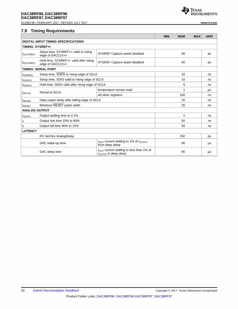
7.9 Timing RequirementsMIN NOM MAX UNIT
DIGITAL INPUT TIMING SPECIFICATIONSTIMING: SYSREF+/-
ts(SYSREF)Setup time, SYSREF+/- valid to risingedge of DACCLK+/- SYSREF Capture assist disabled 50 ps
th(SYSREF)Hold time, SYSREF+/- valid after risingedge of DACCLK+/- SYSREF Capture assist disabled 50 ps
TIMING: SERIAL PORTts(/SDEN) Setup time, SDEN to rising edge of SCLK 20 nsts(SDIO) Setup time, SDIO valid to rising edge of SCLK 10 nsth(SDIO) Hold time, SDIO valid after rising edge of SCLK 5 ns
t(SCLK) Period of SCLKtemperature sensor read 1 µsAll other registers 100 ns
td(Data) Data output delay after falling edge of SCLK 25 nstRESET Minimum RESET pulse width 25 nsANALOG OUTPUTts(DAC) Output settling time to 0.1% 1 nstr Output rise time 10% to 90% 50 nstf Output fall time 90% to 10% 50 nsLATENCY
RX SerDes AnalogDelay 250 ps
DAC wake-up time IOUT current settling to 1% of IOUTFSfrom deep sleep 90 µs
DAC sleep time IOUT current settling to less than 1% ofIOUTFS in deep sleep 90 µs

Output Frequency (MHz)
HD
3 (d
Bc)
500 1000 1500 2000 2500 3000 3500 4000 450035404550556065707580859095
100105
D013
-12dBFS-6dBFS0dBFS
Output Frequency (MHz)
HD
3 (d
Bc)
500 1000 1500 2000 2500 3000 3500 4000 450035404550556065707580859095
100105
D014
Iout=10mAIout=20mAIout=30mAIout=40mA
Output Frequency (MHz)
HD
2 (d
Bc)
500 1000 1500 2000 2500 3000 3500 4000 450035
40
45
50
55
60
65
70
75
80
D018
-12dBFS-6dBFS0dBFS
Output Frequency (MHz)
HD
2 (d
Bc)
500 1000 1500 2000 2500 3000 3500 4000 450035
40
45
50
55
60
65
70
75
80
D023D008D023
Iout=10mAIout=20mAIout=30mAIout=40mA
Output Frequency (MHz)
NS
D (
dBc/
Hz)
500 1000 1500 2000 2500 3000 3500 4000 4500120
126
132
138
144
150
156
162
168
174
180
D005
-12dBFS-9dBFS-6dBFS0dBFS
Output Frequency (MHz)
NS
D (
dBc/
Hz)
500 1000 1500 2000 2500 3000 3500 4000 4500120
126
132
138
144
150
156
162
168
174
180
D011
Iout=40mAIout=30mAIout=20mAIout=10mA
21
DAC38RF86, DAC38RF96DAC38RF87, DAC38RF97
www.ti.com SLASEF4B –FEBRUARY 2017–REVISED JULY 2017
Product Folder Links: DAC38RF86 DAC38RF96 DAC38RF87 DAC38RF97
Submit Documentation FeedbackCopyright © 2017, Texas Instruments Incorporated
7.10 Typical Characteristics, DAC38RF86 and DAC38RF96Unless otherwise noted, all plots are at TA = 25°C, nominal supply voltages, fDAC = 9 GSPS, 12x interpolation, 0dBFS digital input, 40 mA full scale output current , LMFSHd = 84111 and on-chip PLL mode is enabled.
Measured 50 MHz from carrier
Figure 1. NSD vs Output Frequency Over Input Scale
Measured 50 MHz from carrier
Figure 2. NSD vs Output Frequency Over Output CurrentIoutFS
Figure 3. HD2 vs Output Frequency Over Input Scale Figure 4. HD2 vs Output Frequency Over Output CurrentIoutFS
Figure 5. HD3 vs Output Frequency Over Input Scale Figure 6. HD3 vs Output Frequency Over Output CurrentIoutFS

Output Frequency (MHz)
IMD
3 (d
Bc)
500 1000 1500 2000 2500 3000 3500 4000 450035
40
45
50
55
60
65
70
75
80
85
90
D006
-18dBFS-12dBFS-6dBFS0dBFS
Output Frequency (MHz)
HD
3 (d
Bc)
500 1000 1500 2000 2500 3000 3500 4000 450035
40
45
50
55
60
65
70
75
80
D007D007
Iout=10mAIout=20mAIout=30mAIout=40mA
Output Frequency (MHz)
SF
DR
(dB
c)
500 1000 1500 2000 2500 3000 3500 4000 450035
40
45
50
55
60
65
70
75
80
85
90
95
100
D032
-12dBFS-6dBFS0dBFS
Output Frequency (MHz)
SF
DR
(dB
c)
500 1000 1500 2000 2500 3000 3500 4000 450035
40
45
50
55
60
65
70
75
80
85
90
95
100
D008
Iout=10mAIout=20mAIout=30mAIout=40mA
Output Frequency (MHz)
SF
DR
(dB
c)
500 1000 1500 2000 2500 3000 3500 4000 450035
40
45
50
55
60
65
70
75
80
D001D032
-12dBFS-6dBFS0dBFS
Output Frequency (MHz)
SF
DR
(dB
c)
500 1000 1500 2000 2500 3000 3500 4000 450035
40
45
50
55
60
65
70
75
80
D022
Iout=10mAIout=20mAIout=30mAIout=40mA
22
DAC38RF86, DAC38RF96DAC38RF87, DAC38RF97SLASEF4B –FEBRUARY 2017–REVISED JULY 2017 www.ti.com
Product Folder Links: DAC38RF86 DAC38RF96 DAC38RF87 DAC38RF97
Submit Documentation Feedback Copyright © 2017, Texas Instruments Incorporated
Typical Characteristics, DAC38RF86 and DAC38RF96 (continued)
Excludes HD2, HD3 and CMP2
Figure 7. SFDR vs Output Frequency Over Input Scale
Excludes HD2, HD3 and CMP2
Figure 8. SFDR vs Output Frequency Over Output CurrentIoutFS
±250 MHz Span
Figure 9. SFDR vs Output Frequency Over Input Scale
± 250 MHz Span
Figure 10. SFDR vs Output Frequency Over Output CurrentIoutFS
Figure 11. IMD3 vs Output Frequency Over Input Scale Figure 12. IMD3 vs Output Frequency Over Output CurrentIoutFS

Freq offset (Hz)
Pha
se N
oise
(dB
c)
1000 10000 100000 1000000 1E+7 5E+7-160
-140
-120
-100
-80
-60
D007
CP=1CP=2CP=3CP=4CP=5CP=6CP=7CP=8CP=9CP=10CP=11CP=12CP=13CP=14CP=15
Freq offset (Hz)
Pha
se N
oise
(dB
c)
1000 10000 100000 1000000 1E+7 5E+7-160
-150
-140
-130
-120
-110
-100
-90
D008
div4div3div2
Output Frequency (MHz)
Out
put P
ower
(dB
m)
0 500 1000 1500 2000 2500 3000 3500 4000 4500-10-9-8-7-6-5-4-3-2-10123456
D017Output Frequency (MHz)
Isol
atio
n (d
Bc)
500 1000 1500 2000 2500 3000 3500 4000 450050
54
58
62
66
70
74
78
82
86
90
D002
DAC A to BDAC B to A
23
DAC38RF86, DAC38RF96DAC38RF87, DAC38RF97
www.ti.com SLASEF4B –FEBRUARY 2017–REVISED JULY 2017
Product Folder Links: DAC38RF86 DAC38RF96 DAC38RF87 DAC38RF97
Submit Documentation FeedbackCopyright © 2017, Texas Instruments Incorporated
Typical Characteristics, DAC38RF86 and DAC38RF96 (continued)
Figure 13. Power vs Output Frequency Figure 14. Isolation vs Output Frequency
VCO frequency = 8.85 GHz Measured at 1.8 GHz
Figure 15. VCO Phase Noise vs Offset Frequency OverCharge pump current
VCO frequency = 8.85 GHz
Figure 16. VCO1 Output Clock Phase Noise vs Offsetfrequency Over Divider Ratio
Output Frequency (MHz)
HD
3 (d
Bc)
500 750 1000 1250 1500 1750 2000 2250 2500 2750 300050525456586062646668707274767880
D006
-12dBFS-6dBFS0dBFS
Output Frequency (MHz)
HD
3 (d
Bc)
500 750 1000 1250 1500 1750 2000 2250 2500 2750 300060
62
64
66
68
70
72
74
76
78
80
D013
Iout=10mAIout=20mAIout=30mAIout=40mA
Output Frequency (MHz)
HD
2 (d
Bc)
500 750 1000 1250 1500 1750 2000 2250 2500 2750 300035
37.540
42.545
47.550
52.555
57.560
62.565
67.570
72.575
D005
-12dBFS-6dBFS0dBFS
Output Frequency (MHz)
HD
2 (d
Bc)
500 750 1000 1250 1500 1750 2000 2250 2500 2750 300035
37.540
42.545
47.550
52.555
57.560
62.565
67.570
72.575
D012
Iout=10mAIout=20mAIout=30mAIout=40mA
Output Frequency (MHz)
NS
D (
dBF
S/H
z)
500 750 1000 1250 1500 1750 2000 2250 2500 2750 3000140142144146148150152154156158160162164166168170
D007
-12dBFS-9dBFS-6dBFS0dBFS
Output Frequency (MHz)
NS
D (
dBc/
Hz)
500 750 1000 1250 1500 1750 2000 2250 2500 2750 3000140142144146148150152154156158160162164166168170
D014
Iout=40mAIout=30mAIout=20mAIout=10mA
24
DAC38RF86, DAC38RF96DAC38RF87, DAC38RF97SLASEF4B –FEBRUARY 2017–REVISED JULY 2017 www.ti.com
Product Folder Links: DAC38RF86 DAC38RF96 DAC38RF87 DAC38RF97
Submit Documentation Feedback Copyright © 2017, Texas Instruments Incorporated
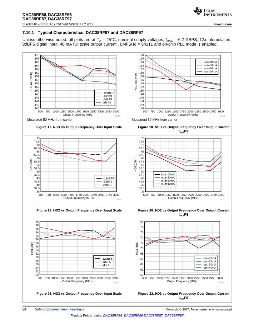
7.10.1 Typical Characteristics, DAC38RF87 and DAC38RF97Unless otherwise noted, all plots are at TA = 25°C, nominal supply voltages, fDAC = 6.2 GSPS, 12x interpolation,0dBFS digital input, 40 mA full scale output current , LMFSHd = 84111 and on-chip PLL mode is enabled.
Measured 50 MHz from carrier
Figure 17. NSD vs Output Frequency Over Input Scale
Measured 50 MHz from carrier
Figure 18. NSD vs Output Frequency Over Output CurrentIoutFS
Figure 19. HD2 vs Output Frequency Over Input Scale Figure 20. HD2 vs Output Frequency Over Output CurrentIoutFS
Figure 21. HD3 vs Output Frequency Over Input Scale Figure 22. HD3 vs Output Frequency Over Output CurrentIoutFS
Output Frequency (MHz)
IMD
3 (d
Bc)
500 750 1000 1250 1500 1750 2000 2250 2500 2750 300045
50
55
60
65
70
75
80
85
90
D008
-18dBFS-12dBFS-6dBFS0dBFS
Output Frequency (MHz)
IMD
3 (d
Bc)
500 750 1000 1250 1500 1750 2000 2250 2500 2750 300065
67
69
71
73
75
77
79
81
83
85
D015
Iout=10mAIout=20mAIout=30mAIout=40mA
Output Frequency (MHz)
SF
DR
(dB
c)
500 750 1000 1250 1500 1750 2000 2250 2500 2750 300035
40
45
50
55
60
65
70
75
80
85
90
95
100
D004
-12dBFS-6dBFS0dBFS
Output Frequency (MHz)
SF
DR
(dB
c)
500 750 1000 1250 1500 1750 2000 2250 2500 2750 300035
40
45
50
55
60
65
70
75
80
85
90
95
100
D011
Iout=10mAIout=20mAIout=30mAIout=40mA
Output Frequency (MHz)
SF
DR
(dB
c)
500 750 1000 1250 1500 1750 2000 2250 2500 2750 300035
37.540
42.545
47.550
52.555
57.560
62.565
67.570
72.575
D003
-12dBFS-6dBFS0dBFS
Output Frequency (MHz)
SF
DR
(dB
c)
500 750 1000 1250 1500 1750 2000 2250 2500 2750 300035
37.540
42.545
47.550
52.555
57.560
62.565
67.570
72.575
D010
Iout=10mAIout=20mAIout=30mAIout=40mA
25
DAC38RF86, DAC38RF96DAC38RF87, DAC38RF97
www.ti.com SLASEF4B –FEBRUARY 2017–REVISED JULY 2017
Product Folder Links: DAC38RF86 DAC38RF96 DAC38RF87 DAC38RF97
Submit Documentation FeedbackCopyright © 2017, Texas Instruments Incorporated
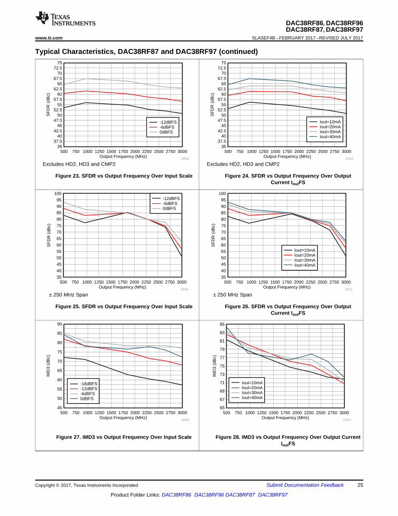
Typical Characteristics, DAC38RF87 and DAC38RF97 (continued)
Excludes HD2, HD3 and CMP2
Figure 23. SFDR vs Output Frequency Over Input Scale
Excludes HD2, HD3 and CMP2
Figure 24. SFDR vs Output Frequency Over OutputCurrent IoutFS
± 250 MHz Span
Figure 25. SFDR vs Output Frequency Over Input Scale
± 250 MHz Span
Figure 26. SFDR vs Output Frequency Over OutputCurrent IoutFS
Figure 27. IMD3 vs Output Frequency Over Input Scale Figure 28. IMD3 vs Output Frequency Over Output CurrentIoutFS

Freq offset (Hz)
Pha
se N
oise
(dB
c)
1000 10000 100000 1000000 1E+7 5E+7-160
-140
-120
-100
-80
D029
CP=1CP=2CP=3CP=4CP=5CP=6CP=7CP=8CP=9CP=10CP=11CP=12CP=13CP=14CP=15
Freq offset (Hz)
Pha
se N
oise
(dB
c)
1000 10000 100000 1000000 1E+7 5E+7-160
-150
-140
-130
-120
-110
-100
D006
div4div3div2
Output Frequency (MHz)
Out
put P
ower
(dB
m)
0 400 800 1200 1600 2000 2400 2800 3200-10
-9
-8
-7
-6
-5
-4
-3
-2
-1
0
1
2
D000Output Frequency (MHz)
Isol
atio
n (d
Bc)
500 1000 1500 2000 2500 3000 3500 4000 450050
54
58
62
66
70
74
78
82
86
90
D002
DAC A to BDAC B to A
26
DAC38RF86, DAC38RF96DAC38RF87, DAC38RF97SLASEF4B –FEBRUARY 2017–REVISED JULY 2017 www.ti.com
Product Folder Links: DAC38RF86 DAC38RF96 DAC38RF87 DAC38RF97
Submit Documentation Feedback Copyright © 2017, Texas Instruments Incorporated
Typical Characteristics, DAC38RF87 and DAC38RF97 (continued)
Figure 29. Power vs Output Frequency Figure 30. Isolation vs Output Frequency
VCO frequency = 5.9 GHz measured at 1.8 GHz
Figure 31. VCO Phase Noise vs Offset Frequency OverCharge Pump Current
VCO frequency = 5.9 GHz
Figure 32. VCO Output clock Phase Noise vs OffsetFrequency Over Divider Ratio
14-b
DAC
Control InterfaceTemp
Sensor
Clock
Distribution
RBIAS
DACCLK+
DACCLK-
RX[4..7]+
RX[4..7]-
RX[0..3]+
RX[0..3]-
SYSREF+
SYSREF-
SDO
SDIO
SDENB
SCLK
TXENABLE
RESETB
VDDCLK1
VDDDIG1
VDDA18
GND
DACB
Gain
Low Jitter
PLL
ALA
RM
SLEEP
SYNC1\+
SYNC1\-
TESTMODE
VDDAVCO18
VDDAPLL1
VDDIO18
0.9 V
Ref
VDDA1
VDDS18
VDDT1
VDDR18
JTAG
TCLK TDI
TDO
TMS
TRST\
ATESTAMUX0/1
IFORCE
VSENSE
TESTMODE
VEE18N
VOUT2
CLKTX+Divider
/2, /3, /4
JES
D I
nte
rfa
ce
Multi-band DUC Channel 1 (multi-DUC1)
x
sin(x)
14-b
DAC
DACA
Gain
VOUT1x
sin(x)
I
Q
I
Q
I
Q
I
Q
NCO 1
NCO 2
NCO 4
NCO 3
Multi-band DUC Channel 2 (multi-DUC2)
CLKTX-
VDDAPLL18
SYNC2\+
SYNC2\-
GPO0
GPO1
GPI0
GPI1
VDDL1_1
VDDL2_1
DACCLKSE VDDTX1
VDDTX18
VDDOUT18
Copyright © 2016, Texas Instruments Incorporated
EXTIO
VDDE1
27
DAC38RF86, DAC38RF96DAC38RF87, DAC38RF97
www.ti.com SLASEF4B –FEBRUARY 2017–REVISED JULY 2017
Product Folder Links: DAC38RF86 DAC38RF96 DAC38RF87 DAC38RF97
Submit Documentation FeedbackCopyright © 2017, Texas Instruments Incorporated
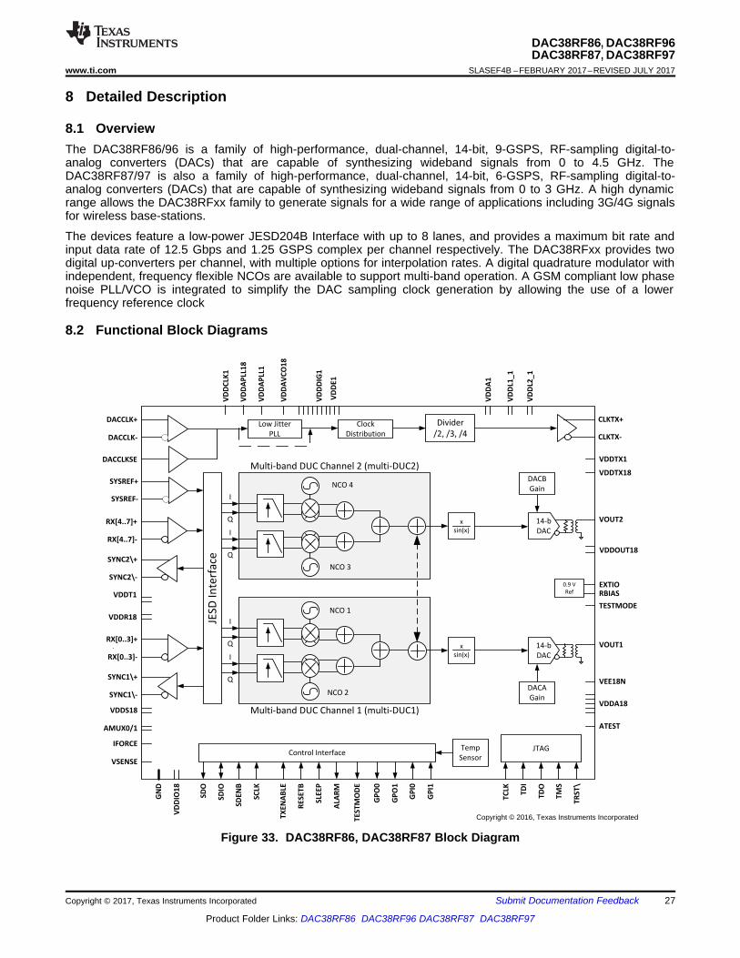
8 Detailed Description
8.1 OverviewThe DAC38RF86/96 is a family of high-performance, dual-channel, 14-bit, 9-GSPS, RF-sampling digital-to-analog converters (DACs) that are capable of synthesizing wideband signals from 0 to 4.5 GHz. TheDAC38RF87/97 is also a family of high-performance, dual-channel, 14-bit, 6-GSPS, RF-sampling digital-to-analog converters (DACs) that are capable of synthesizing wideband signals from 0 to 3 GHz. A high dynamicrange allows the DAC38RFxx family to generate signals for a wide range of applications including 3G/4G signalsfor wireless base-stations.
The devices feature a low-power JESD204B Interface with up to 8 lanes, and provides a maximum bit rate andinput data rate of 12.5 Gbps and 1.25 GSPS complex per channel respectively. The DAC38RFxx provides twodigital up-converters per channel, with multiple options for interpolation rates. A digital quadrature modulator withindependent, frequency flexible NCOs are available to support multi-band operation. A GSM compliant low phasenoise PLL/VCO is integrated to simplify the DAC sampling clock generation by allowing the use of a lowerfrequency reference clock
8.2 Functional Block Diagrams
Figure 33. DAC38RF86, DAC38RF87 Block Diagram

14-b
DAC
Control InterfaceTemp
Sensor
Clock
Distribution
DACCLK+
DACCLK-
RX[4..7]+
RX[4..7]-
RX[0..3]+
RX[0..3]-
SYSREF+
SYSREF-
SDO
SDIO
SDENB
SCLK
TXENABLE
RESETB
VDDCLK1
VDDDIG1
VDDA18
GND
DACB
Gain
Low Jitter
PLL
ALA
RM
SLEEP
SYNC1\+
SYNC1\-
TESTMODE
VDDAVCO18
VDDAPLL1
VDDIO18
VDDA1
VDDS18
VDDT1
VDDR18
JTAG
TCLK TDI
TDO
TMS
TRST\
ATESTAMUX0/1
IFORCE
VSENSE
VEE18N
VOUT2
CLKTX+Divider
/2, /3, /4JE
SD
In
terf
ace
Single-band DUC Channel 1
x
sin(x)
14-b
DAC
DACA
Gain
VOUT1x
sin(x)
I
Q
I
Q
NCO 1
NCO 2
Single-band DUC Channel 2
CLKTX-
VDDAPLL18
SYNC2\+
SYNC2\-
GPO0
GPO1
GPI0
GPI1
VDDL1_1
VDDL2_1
DACCLKSE VDDTX1
VDDTX18
VDDOUT18
Copyright © 2016, Texas Instruments Incorporated
RBIAS
0.9 V
Ref
TESTMODE
EXTIO
VDDE1
28
DAC38RF86, DAC38RF96DAC38RF87, DAC38RF97SLASEF4B –FEBRUARY 2017–REVISED JULY 2017 www.ti.com
Product Folder Links: DAC38RF86 DAC38RF96 DAC38RF87 DAC38RF97
Submit Documentation Feedback Copyright © 2017, Texas Instruments Incorporated
Functional Block Diagrams (continued)
Figure 34. DAC38RF96, DAC38RF97 Block Diagram
0.7V
0.25V
50pF
50O
50O
TERM
=100
TERM
=001
TERM
=101
Level
Shift
RXP
RXN
To
Equalizer
&
Samplers
29
DAC38RF86, DAC38RF96DAC38RF87, DAC38RF97
www.ti.com SLASEF4B –FEBRUARY 2017–REVISED JULY 2017
Product Folder Links: DAC38RF86 DAC38RF96 DAC38RF87 DAC38RF97
Submit Documentation FeedbackCopyright © 2017, Texas Instruments Incorporated
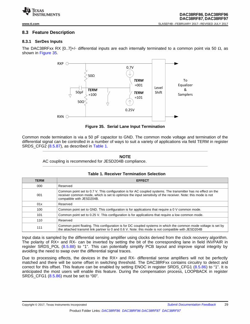
8.3 Feature Description
8.3.1 SerDes InputsThe DAC38RFxx RX [0..7]+/- differential inputs are each internally terminated to a common point via 50 Ω, asshown in Figure 35.
Figure 35. Serial Lane Input Termination
Common mode termination is via a 50 pF capacitor to GND. The common mode voltage and termination of thedifferential signal can be controlled in a number of ways to suit a variety of applications via field TERM in registerSRDS_CFG2 (8.5.87), as described in Table 1.
NOTEAC coupling is recommended for JESD204B compliance.
Table 1. Receiver Termination SelectionTERM EFFECT
000 Reserved
001Common point set to 0.7 V. This configuration is for AC coupled systems. The transmitter has no effect on thereceiver common mode, which is set to optimize the input sensitivity of the receiver. Note: this mode is notcompatible with JESD204B.
01x Reserved100 Common point set to GND. This configuration is for applications that require a 0 V common mode.101 Common point set to 0.25 V. This configuration is for applications that require a low common mode.110 Reserved
111 Common point floating. This configuration is for DC coupled systems in which the common mode voltage is set bythe attached transmit link partner to 0 and 0.6 V. Note: this mode is not compatible with JESD204B
Input data is sampled by the differential sensing amplifier using clocks derived from the clock recovery algorithm.The polarity of RX+ and RX- can be inverted by setting the bit of the corresponding lane in field INVPAIR inregister SRDS_POL (8.5.88) to “1”. This can potentially simplify PCB layout and improve signal integrity byavoiding the need to swap over the differential signal traces.
Due to processing effects, the devices in the RX+ and RX- differential sense amplifiers will not be perfectlymatched and there will be some offset in switching threshold. The DAC38RFxx contains circuitry to detect andcorrect for this offset. This feature can be enabled by setting ENOC in register SRDS_CFG1 (8.5.86) to “1”. It isanticipated the most users will enable this feature. During the compensation process, LOOPBACK in registerSRDS_CFG1 (8.5.86) must be set to “00”.
DACCLK+
DACCLK-
DACCLKSE
0
1
SEL_EXTCLK_DIFFSE
DAC PLL
Predivider 0
1
SERDES_REFCLK_SEL
divider
SERDES_REFCLK_DIV
SERDES_REFCLK_PREDIV
SERDESPLL
REFCLK
30
DAC38RF86, DAC38RF96DAC38RF87, DAC38RF97SLASEF4B –FEBRUARY 2017–REVISED JULY 2017 www.ti.com
Product Folder Links: DAC38RF86 DAC38RF96 DAC38RF87 DAC38RF97
Submit Documentation Feedback Copyright © 2017, Texas Instruments Incorporated
8.3.2 SerDes RateThe DAC38RFxx has eight configurable JESD204B serial lanes. The highest speed of each SerDes lane is 12.5Gbps. Because the primary operating frequency of the SerDes is determined by its reference clock and PLLmultiplication factor, there is a limit on the lowest SerDes rate supported. To support lower speed application,each receiver should be configured to operate at half, quarter or eighth of the full rate via field RATE in registerSRDS_CFG2 (8.5.87). Refer to Table 2 for details.
Table 2. Lane Rate SelectionRATE EFFECT
00 Full rate. Four data samples taken per SerDes PLL output clock cycle.01 Half rate. Two data samples taken per SerDes PLL output clock cycle.10 Quarter rate. One data samples taken per SerDes PLL output clock cycle.11 Eighth rate. One data samples taken every two SerDes PLL output clock cycles.
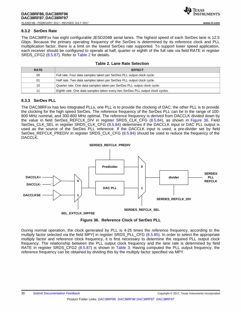
8.3.3 SerDes PLLThe DAC38RFxx has two integrated PLLs, one PLL is to provide the clocking of DAC; the other PLL is to providethe clocking for the high speed SerDes. The reference frequency of the SerDes PLL can be in the range of 100-800 MHz nominal, and 300-800 MHz optimal. The reference frequency is derived from DACCLK divided down bythe value in field SerDes_REFCLK_DIV in register SRDS_CLK_CFG (8.5.84), as shown in Figure 36. FieldSerDes_CLK_SEL in register SRDS_CLK_CFG (8.5.84) determines if the DACCLK input or DAC PLL output isused as the source of the SerDes PLL reference. If the DACCLK input is used, a pre-divider set by fieldSerDes_REFCLK_PREDIV in register SRDS_CLK_CFG (8.5.84) should be used to reduce the frequency of theDACCLK.
Figure 36. Reference Clock of SerDes PLL
During normal operation, the clock generated by PLL is 4-25 times the reference frequency, according to themultiply factor selected via the field MPY] in register SRDS_PLL_CFG (8.5.85). In order to select the appropriatemultiply factor and reference clock frequency, it is first necessary to determine the required PLL output clockfrequency. The relationship between the PLL output clock frequency and the lane rate is determined by fieldRATE in register SRDS_CFG2 (8.5.87) is shown in Table 3. Having computed the PLL output frequency, thereference frequency can be obtained by dividing this by the multiply factor specified via MPY.
31
DAC38RF86, DAC38RF96DAC38RF87, DAC38RF97
www.ti.com SLASEF4B –FEBRUARY 2017–REVISED JULY 2017
Product Folder Links: DAC38RF86 DAC38RF96 DAC38RF87 DAC38RF97
Submit Documentation FeedbackCopyright © 2017, Texas Instruments Incorporated
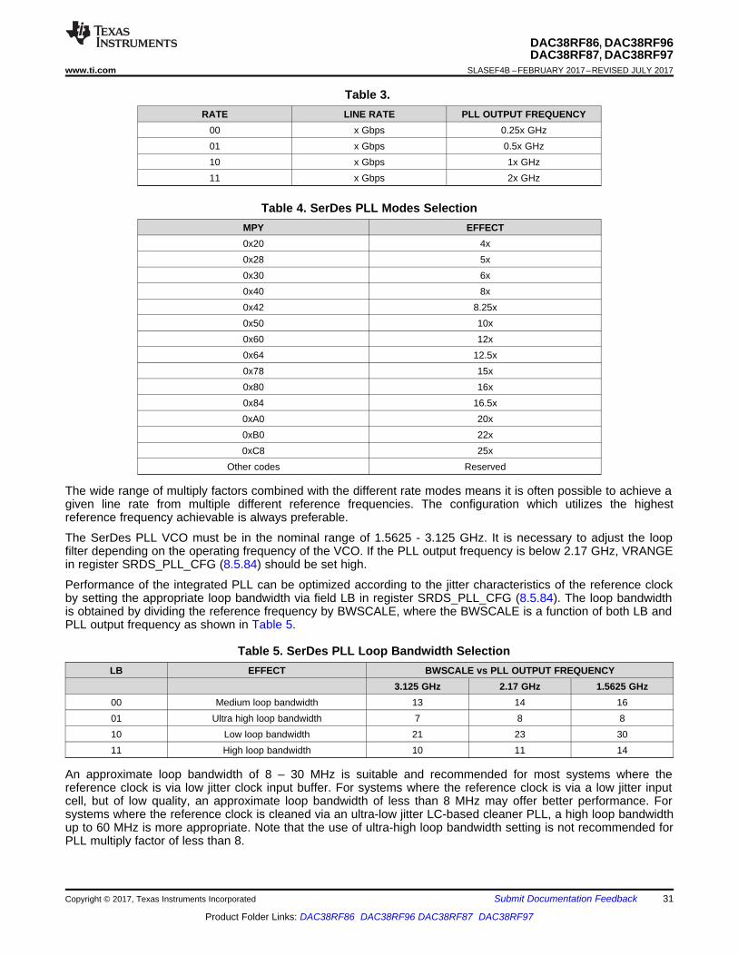
Table 3.RATE LINE RATE PLL OUTPUT FREQUENCY
00 x Gbps 0.25x GHz01 x Gbps 0.5x GHz10 x Gbps 1x GHz11 x Gbps 2x GHz
Table 4. SerDes PLL Modes SelectionMPY EFFECT0x20 4x0x28 5x0x30 6x0x40 8x0x42 8.25x0x50 10x0x60 12x0x64 12.5x0x78 15x0x80 16x0x84 16.5x0xA0 20x0xB0 22x0xC8 25x
Other codes Reserved
The wide range of multiply factors combined with the different rate modes means it is often possible to achieve agiven line rate from multiple different reference frequencies. The configuration which utilizes the highestreference frequency achievable is always preferable.
The SerDes PLL VCO must be in the nominal range of 1.5625 - 3.125 GHz. It is necessary to adjust the loopfilter depending on the operating frequency of the VCO. If the PLL output frequency is below 2.17 GHz, VRANGEin register SRDS_PLL_CFG (8.5.84) should be set high.
Performance of the integrated PLL can be optimized according to the jitter characteristics of the reference clockby setting the appropriate loop bandwidth via field LB in register SRDS_PLL_CFG (8.5.84). The loop bandwidthis obtained by dividing the reference frequency by BWSCALE, where the BWSCALE is a function of both LB andPLL output frequency as shown in Table 5.
Table 5. SerDes PLL Loop Bandwidth SelectionLB EFFECT BWSCALE vs PLL OUTPUT FREQUENCY
3.125 GHz 2.17 GHz 1.5625 GHz00 Medium loop bandwidth 13 14 1601 Ultra high loop bandwidth 7 8 810 Low loop bandwidth 21 23 3011 High loop bandwidth 10 11 14
An approximate loop bandwidth of 8 – 30 MHz is suitable and recommended for most systems where thereference clock is via low jitter clock input buffer. For systems where the reference clock is via a low jitter inputcell, but of low quality, an approximate loop bandwidth of less than 8 MHz may offer better performance. Forsystems where the reference clock is cleaned via an ultra-low jitter LC-based cleaner PLL, a high loop bandwidthup to 60 MHz is more appropriate. Note that the use of ultra-high loop bandwidth setting is not recommended forPLL multiply factor of less than 8.
108 414 Log10MHz
Gain
-6.3
6
dB
Frequency
32
DAC38RF86, DAC38RF96DAC38RF87, DAC38RF97SLASEF4B –FEBRUARY 2017–REVISED JULY 2017 www.ti.com
Product Folder Links: DAC38RF86 DAC38RF96 DAC38RF87 DAC38RF97
Submit Documentation Feedback Copyright © 2017, Texas Instruments Incorporated
A free running clock output is available when field ENDIVCLK in register SRDS_PLL_CFG (8.5.85) is set high. Itruns at a fixed divided-by-80 of the PLL output frequency and can be output on the ALARM pin by setting fieldDTEST to “0001” (lanes 0 – 3) or “0010” (lanes 4 – 7) in register DTEST (8.5.76).
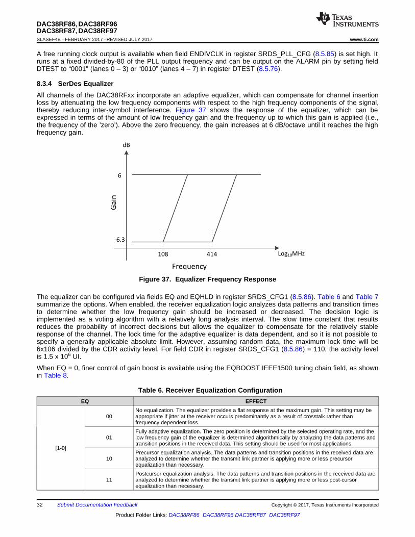
8.3.4 SerDes EqualizerAll channels of the DAC38RFxx incorporate an adaptive equalizer, which can compensate for channel insertionloss by attenuating the low frequency components with respect to the high frequency components of the signal,thereby reducing inter-symbol interference. Figure 37 shows the response of the equalizer, which can beexpressed in terms of the amount of low frequency gain and the frequency up to which this gain is applied (i.e.,the frequency of the ’zero’). Above the zero frequency, the gain increases at 6 dB/octave until it reaches the highfrequency gain.
Figure 37. Equalizer Frequency Response
The equalizer can be configured via fields EQ and EQHLD in register SRDS_CFG1 (8.5.86). Table 6 and Table 7summarize the options. When enabled, the receiver equalization logic analyzes data patterns and transition timesto determine whether the low frequency gain should be increased or decreased. The decision logic isimplemented as a voting algorithm with a relatively long analysis interval. The slow time constant that resultsreduces the probability of incorrect decisions but allows the equalizer to compensate for the relatively stableresponse of the channel. The lock time for the adaptive equalizer is data dependent, and so it is not possible tospecify a generally applicable absolute limit. However, assuming random data, the maximum lock time will be6x106 divided by the CDR activity level. For field CDR in register SRDS_CFG1 (8.5.86) = 110, the activity levelis 1.5 x 10⁶ UI.
When EQ = 0, finer control of gain boost is available using the EQBOOST IEEE1500 tuning chain field, as shownin Table 8.
Table 6. Receiver Equalization ConfigurationEQ EFFECT
[1-0]
00No equalization. The equalizer provides a flat response at the maximum gain. This setting may beappropriate if jitter at the receiver occurs predominantly as a result of crosstalk rather thanfrequency dependent loss.
01Fully adaptive equalization. The zero position is determined by the selected operating rate, and thelow frequency gain of the equalizer is determined algorithmically by analyzing the data patterns andtransition positions in the received data. This setting should be used for most applications.
10Precursor equalization analysis. The data patterns and transition positions in the received data areanalyzed to determine whether the transmit link partner is applying more or less precursorequalization than necessary.
11Postcursor equalization analysis. The data patterns and transition positions in the received data areanalyzed to determine whether the transmit link partner is applying more or less post-cursorequalization than necessary.
33
DAC38RF86, DAC38RF96DAC38RF87, DAC38RF97
www.ti.com SLASEF4B –FEBRUARY 2017–REVISED JULY 2017
Product Folder Links: DAC38RF86 DAC38RF96 DAC38RF87 DAC38RF97
Submit Documentation FeedbackCopyright © 2017, Texas Instruments Incorporated
Table 6. Receiver Equalization Configuration (continued)EQ EFFECT
[2]0 Default
1 Boost. Equalizer gain boosted by 6 dB, with a 20% reduction in bandwidth, and an increase of5mW power consumption. May improve performance over long links.
Table 7. Receiver Equalizer HoldEQHOLD EFFECT
0 Equalizer adaption enabled. The equalizer adaption and analysis algorithm is enabled. This should be the defaultstate.
1 Equalizer adaption held. The equalizer is held in its current state. Additionally, the adaption and analysis algorithmis reset.
Table 8. Relationship Between Lane Rate and SerDes PLL Output FrequencyEQBOOST GAIN BOOST (dB) BANDWIDTH CHANGE (%) POWER INCREASE (mW)
00 0 0 001 2 -30 001 4 10 511 6 -20 5
When EQ is set to 010 or 011, the equalizer is reconfigured to provide analytical data about the amount of preand post cursor equalization respectively present in the received signal. This can in turn be used to adjust theequalization settings of the transmitting link partner, where a suitable mechanism for communicating this databack to the transmitter exists. Status information is provided by setting field DTEST in register DTEST (8.5.76) to“0111” for EQOVER and “0110” for EQUNDER. The procedure is as follows:1. Enable the equalizer by setting fields EQHLD low and EQ to “001” (register SRDS_CFG1 8.5.86). Allow
sufficient time for the equalizer to adapt;2. Set EQHLD to 1 to lock the equalizer and reset the adaption algorithm. This also causes both EQOVER and
EQUNDER to become low;3. Wait at least 48 UI, and proportionately longer if the CDR activity is less than 100%, to ensure the 1 on
EQHLD is sampled and acted upon;4. Set EQ to “010” or “011”, and EQHLD to 0. The equalization characteristics of the received signal are
analysed (the equalizer response will continue to be locked);5. Wait at least 150 × 103 UI to allow time for the analysis to occur, proportionately longer if the CDR activity is
less than 100%;6. Examine EQOVER and EQUNDER for results of analysis
– If EQOVER is high, it indicates the signal is over equalized;– If EQUNDER is high, it indicates the signal is under equalized;
7. Set EQHLD to 1;8. Repeat items 3–7 if required;9. Set EQ to “001”, and EQHLD to 0 to exit analysis mode and return to normal adaptive equalization.
NOTEWhen changing EQ from one non-zero value to another, EQHLD must already be 1. If thisis not the case, there is a chance the equalizer could be reset by a transitory input state(i.e., if EQ is momentarily 000). EQHLD can be set to 0 at the same time as EQ ischanged.
As the equalizer adaption algorithm is designed to equalize the post cursor, EQOVER orEQUNDER will only be set during post cursor analysis if the amount of post cursorequalization required is more or less than the adaptive equalizer can provide.
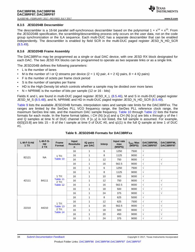
34
DAC38RF86, DAC38RF96DAC38RF87, DAC38RF97SLASEF4B –FEBRUARY 2017–REVISED JULY 2017 www.ti.com
Product Folder Links: DAC38RF86 DAC38RF96 DAC38RF87 DAC38RF97
Submit Documentation Feedback Copyright © 2017, Texas Instruments Incorporated
8.3.5 JESD204B DescramblerThe descrambler is a 16-bit parallel self-synchronous descrambler based on the polynomial 1 + x14 + x15. Fromthe JESD204B specification, the scrambling/descrambling process only occurs on the user data, not on the codegroup synchronization or the ILA sequence. Each multi-DUC has a separate descrambler that can be enabledindependently. The descrambler is enabled by field SCR in the multi-DUC paged register JESD_N_HD_SCR(8.5.49).
8.3.6 JESD204B Frame AssemblyThe DAC38RFxx may be programmed as a single or dual DAC device, with one JESD RX block designated foreach DAC. The two JESD RX blocks can be programmed to operate as two separate links or as a single link.
The JESD204B defines the following parameters:• L is the number of lanes• M is the number of I or Q streams per device (2 = 1 IQ pair, 4 = 2 IQ pairs, 8 = 4 IQ pairs)• F is the number of octets per frame clock period• S is the number of samples per frame• HD is the High-Density bit which controls whether a sample may be divided over more lanes• N = NPRIME is the number of bits per sample (12 or 16 - bits)
Fields K and L are found in multi-DUC paged register JESD_K_L (8.5.46), M and S in multi-DUC paged registerJESD_M_S (8.5.48), and N, NPRIME and HD in multi-DUC paged register JESD_N_HD_SCR (8.5.49).
Table 9 lists the available JESD204B formats, interpolation rates and sample rate limits for the DAC38RFxx. Theranges are limited by the SerDes PLL VCO frequency range, the SerDes PLL reference clock range, themaximum SerDes line rate, and the maximum DAC sample frequency. Table 10 through Table 22 lists the frameformats for each mode. In the frame format tables, i CH (N) [x:y] and q CH (N) [x:y] are bits x through y of the Iand Q samples at time N of DUC channel CH. If [x..y] is not listed, the full sample is assumed. For example,i0(0)[15:8] are bits 15 – 8 of the I sample at time 0 of DUC #0, and q1(1) is the full Q sample at time 1 of DUC#1.
Table 9. JESD204B Formats for DAC38RFxx
L-M-F-S-Hd1 TX
L-M-F-S-Hd
2 TXFrameFormat
InputResolutio
nIQ pairsper DAC Interp
Input ratemax
(MSPS)fDAC Max(MSPS)
DAC38RF86,DAC38RF87
DAC38RF96,DAC38RF97
82121 NA 1 TX:Table 10
16 1 6 1250 7500 √16 1 8 1125 9000 √16 1 12 750 9000 √ √16 1 16 562.5 9000 √ √
42111 84111
1 TX:Table 11
2 TX:Table 12
16 1 6 1250 7500 √16 1 8 1125 9000 √16 1 10 900 9000 √16 1 12 750 9000 √ √16 1 16 562.5 9000 √ √16 1 18 500 9000 √ √16 1 24 375 9000 √ √
22210 44210
1 TX:Table 13
2 TX:Table 14
16 1 8 625 5000 √16 1 12 625 7500 √ √16 1 16 562.5 9000 √ √16 1 18 500 9000 √ √16 1 20 450 9000 √ √16 1 24 375 9000 √ √

35
DAC38RF86, DAC38RF96DAC38RF87, DAC38RF97
www.ti.com SLASEF4B –FEBRUARY 2017–REVISED JULY 2017
Product Folder Links: DAC38RF86 DAC38RF96 DAC38RF87 DAC38RF97
Submit Documentation FeedbackCopyright © 2017, Texas Instruments Incorporated
L-M-F-S-Hd1 TX
L-M-F-S-Hd
2 TXFrameFormat
InputResolutio
nIQ pairsper DAC Interp
Input ratemax
(MSPS)fDAC Max(MSPS)
DAC38RF86,DAC38RF87
DAC38RF96,DAC38RF97
12410 24410
1 TX:Table 15
2 TX:Table 16
16 1 16 312.5 5000 √ √
16 1 24 312.5 7500 √ √
44210 88210
1 TX:Table 17
2 TX:Table 18
16 2 8 625 5000 √16 2 12 625 7500 √16 2 16 562.5 9000 √16 2 24 375 9000 √
24410 48410
1 TX:Table 19
2 TX:Table 20
16 2 16 312.5 5000 √
16 2 24 312.5 7500 √
24310 48310
1 TX:Table 21
2 TX:Table 22
12 2 24 375 9000 √
Table 10. JESD204B Frame Format for LMFSHd = 82121# un bits 4 8# en bits 5 10Nibble 1 2
lane RX0 i0[15:8]lane RX1 i0[7:0]lane RX2 i1[15:8]lane RX3 i1[7:0]lane RX4 q0[15:8]lane RX5 q0[7:0]lane RX6 q1[15:8]lane RX7 q1[7:0]
Table 11. JESD204B Frame Format for LMFSHd = 42111# un bits 4 8# en bits 5 10Nibble 1 2
lane RX0 i0[15:8]lane RX1 i0[7:0]lane RX2 q0[15:8]lane RX3 q0[7:0]
(1) DAC A, I sample 0, MSB byte(2) DAC A, I sample 0, LSB byte
Table 12. JESD204B Frame Format for LMFSHd = 84111# un bits 4 8# en bits 5 10Nibble 1 2
lane RX0 A-i0[15:8] (1)
lane RX1 A-i0[7:0] (2)
lane RX2 A-q0[15:8]lane RX3 A-q0[7:0]lane RX4 B-i0[15:8]
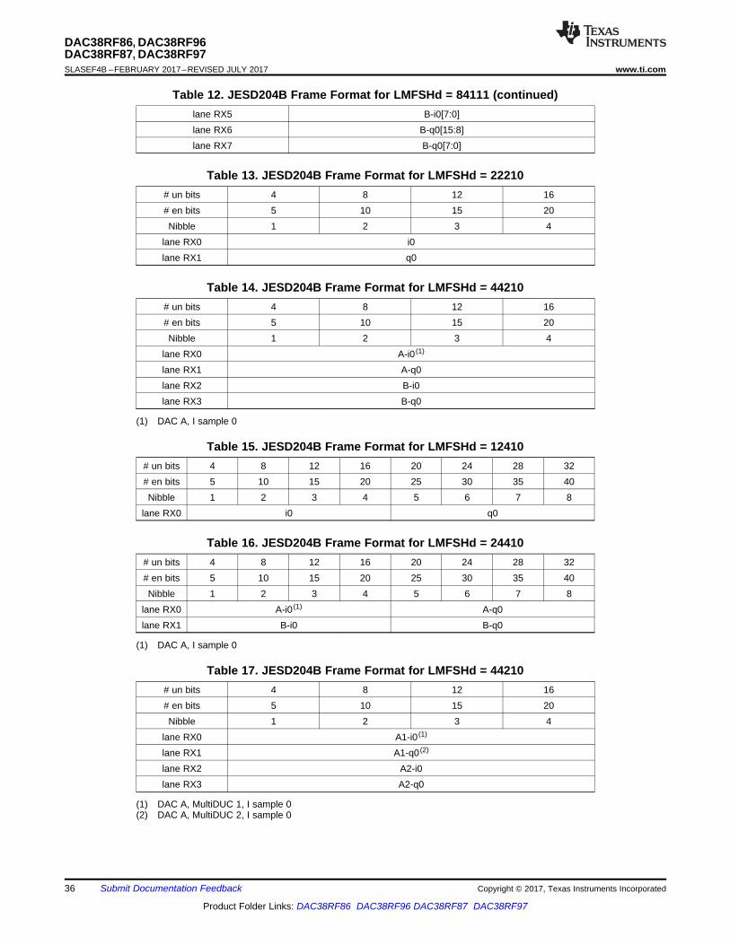
36
DAC38RF86, DAC38RF96DAC38RF87, DAC38RF97SLASEF4B –FEBRUARY 2017–REVISED JULY 2017 www.ti.com
Product Folder Links: DAC38RF86 DAC38RF96 DAC38RF87 DAC38RF97
Submit Documentation Feedback Copyright © 2017, Texas Instruments Incorporated
Table 12. JESD204B Frame Format for LMFSHd = 84111 (continued)lane RX5 B-i0[7:0]lane RX6 B-q0[15:8]lane RX7 B-q0[7:0]
Table 13. JESD204B Frame Format for LMFSHd = 22210# un bits 4 8 12 16# en bits 5 10 15 20Nibble 1 2 3 4
lane RX0 i0lane RX1 q0
(1) DAC A, I sample 0
Table 14. JESD204B Frame Format for LMFSHd = 44210# un bits 4 8 12 16# en bits 5 10 15 20Nibble 1 2 3 4
lane RX0 A-i0 (1)
lane RX1 A-q0lane RX2 B-i0lane RX3 B-q0
Table 15. JESD204B Frame Format for LMFSHd = 12410# un bits 4 8 12 16 20 24 28 32# en bits 5 10 15 20 25 30 35 40Nibble 1 2 3 4 5 6 7 8
lane RX0 i0 q0
(1) DAC A, I sample 0
Table 16. JESD204B Frame Format for LMFSHd = 24410# un bits 4 8 12 16 20 24 28 32# en bits 5 10 15 20 25 30 35 40Nibble 1 2 3 4 5 6 7 8
lane RX0 A-i0 (1) A-q0lane RX1 B-i0 B-q0
(1) DAC A, MultiDUC 1, I sample 0(2) DAC A, MultiDUC 2, I sample 0
Table 17. JESD204B Frame Format for LMFSHd = 44210# un bits 4 8 12 16# en bits 5 10 15 20Nibble 1 2 3 4
lane RX0 A1-i0 (1)
lane RX1 A1-q0 (2)
lane RX2 A2-i0lane RX3 A2-q0
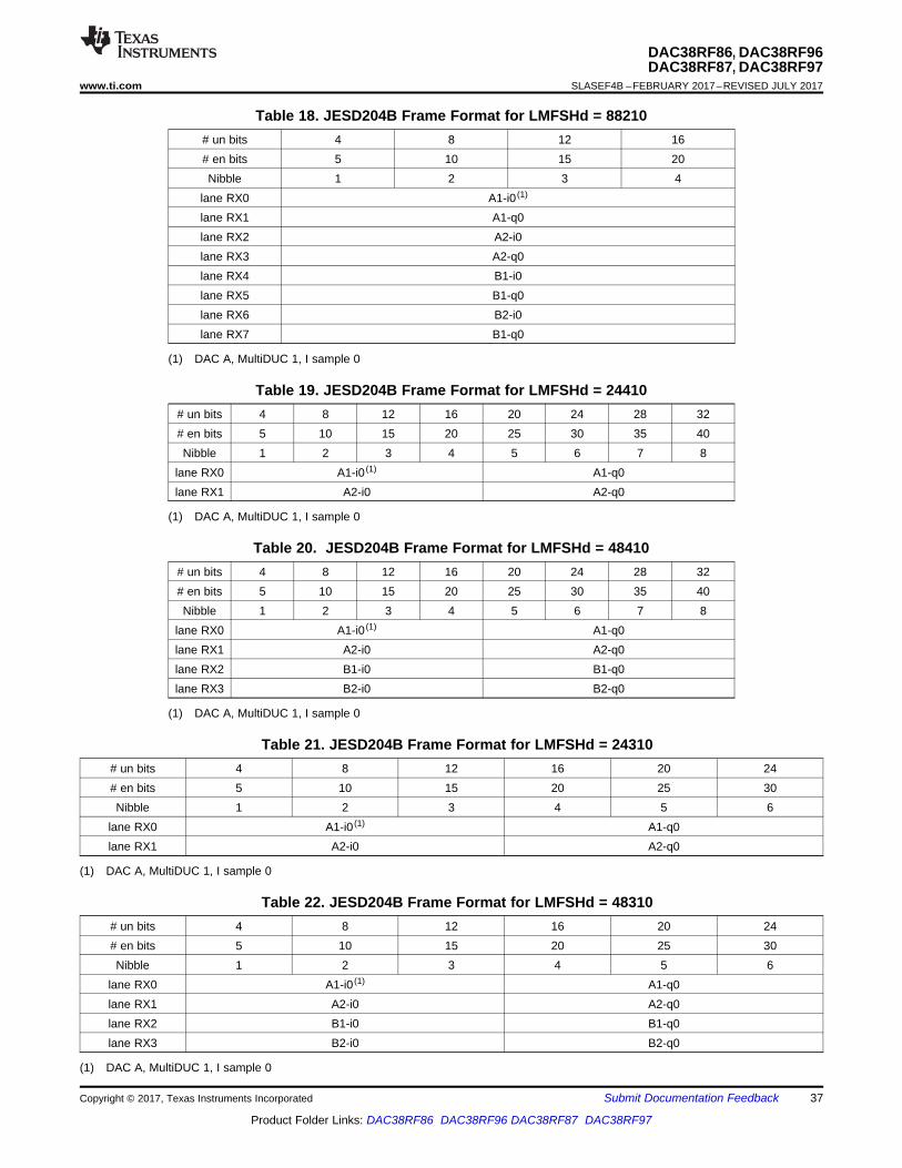
37
DAC38RF86, DAC38RF96DAC38RF87, DAC38RF97
www.ti.com SLASEF4B –FEBRUARY 2017–REVISED JULY 2017
Product Folder Links: DAC38RF86 DAC38RF96 DAC38RF87 DAC38RF97
Submit Documentation FeedbackCopyright © 2017, Texas Instruments Incorporated
(1) DAC A, MultiDUC 1, I sample 0
Table 18. JESD204B Frame Format for LMFSHd = 88210# un bits 4 8 12 16# en bits 5 10 15 20Nibble 1 2 3 4
lane RX0 A1-i0 (1)
lane RX1 A1-q0lane RX2 A2-i0lane RX3 A2-q0lane RX4 B1-i0lane RX5 B1-q0lane RX6 B2-i0lane RX7 B1-q0
(1) DAC A, MultiDUC 1, I sample 0
Table 19. JESD204B Frame Format for LMFSHd = 24410# un bits 4 8 12 16 20 24 28 32# en bits 5 10 15 20 25 30 35 40Nibble 1 2 3 4 5 6 7 8
lane RX0 A1-i0 (1) A1-q0lane RX1 A2-i0 A2-q0
(1) DAC A, MultiDUC 1, I sample 0
Table 20. JESD204B Frame Format for LMFSHd = 48410# un bits 4 8 12 16 20 24 28 32# en bits 5 10 15 20 25 30 35 40Nibble 1 2 3 4 5 6 7 8
lane RX0 A1-i0 (1) A1-q0lane RX1 A2-i0 A2-q0lane RX2 B1-i0 B1-q0lane RX3 B2-i0 B2-q0
(1) DAC A, MultiDUC 1, I sample 0
Table 21. JESD204B Frame Format for LMFSHd = 24310# un bits 4 8 12 16 20 24# en bits 5 10 15 20 25 30Nibble 1 2 3 4 5 6
lane RX0 A1-i0 (1) A1-q0lane RX1 A2-i0 A2-q0
(1) DAC A, MultiDUC 1, I sample 0
Table 22. JESD204B Frame Format for LMFSHd = 48310# un bits 4 8 12 16 20 24# en bits 5 10 15 20 25 30Nibble 1 2 3 4 5 6
lane RX0 A1-i0 (1) A1-q0lane RX1 A2-i0 A2-q0lane RX2 B1-i0 B1-q0lane RX3 B2-i0 B2-q0

38
DAC38RF86, DAC38RF96DAC38RF87, DAC38RF97SLASEF4B –FEBRUARY 2017–REVISED JULY 2017 www.ti.com
Product Folder Links: DAC38RF86 DAC38RF96 DAC38RF87 DAC38RF97
Submit Documentation Feedback Copyright © 2017, Texas Instruments Incorporated
8.3.7 SYNC InterfaceThe DAC38RFxx JESD204B interface has two differential SYNC outputs called SYNC0 and SYNC1 to supportone or two links. Alternatively, GPO0 and GPO1 can be used to output SYNC as a single-ended CMOS level.Each of the differential or CMOS outputs is enabled by a 2-bit register (fields GPO0_SEL, GPO1_SEL,SYNC0B_SEL, SYNC1B_SEL in register IO_CONFIG 8.5.2), with bit 0 enabling multi-DUC1 SYNC and bit 1enabling multi-DUC2 SYNC. If both are enabled, the SYNC\ signals are OR’ed.
The SYNC signal can be asserted low by the receiver either to make a synchronization request toinitialize/reinitialize the link or to report an error to the transmitter. Synchronization requests must have aminimum duration of five frames plus nine octets rounded up to the nearest whole number of frames. To reportan error, the SYNC signal is asserted for exactly two frames. The transmitter interprets any negative edge of itsSYNC input as an error and any SYNC assertion lasting four frames or longer as a synchronization request. Seethe following sections in the standard for more details.• 7.6.3 Errors requiring re-initialization• 7.6.4 Error reporting via SYNC interface• 8.4 SYNC signal decoding
8.3.8 Single or Dual Link ConfigurationThe DAC38RFxx JESD204B interface can be configures with one or two links. The advantage of using two links,one for each DAC, is that one link can be re-established without affecting the other link and DAC.
The configuration for each mode of operation are:1. Dual DAC, dual link
(a) Program fields OCTETPATH0_SEL to OCTETPATH7_SEL in multi-DUC paged registersJESD_CROSSBAR1 (8.5.57) and JESD_CROSSBAR2 (8.5.58) so that each multi-DUC will pick data offof the appropriate SerDes lane.
(b) Appropriate bits in field LANE_ENA in multi-DUC paged register JESD_LN_EN (8.5.45) must be set foreach multi-DUC enable the lanes used.
(c) Field ONE_DAC_ONLY in register RESET_CONFIG (8.5.1) should be ‘0’ (default).2. Dual DAC, single link
(a) Program OCTETPATH0_SEL to OCTETPATH7_SEL in multi-DUC paged registers JESD_CROSSBAR1(8.5.57) and JESD_CROSSBAR2 (8.5.58) so that each multi-DUC will pick data off the appropriateSerDes lane.
(b) Appropriate bits in field LANE_ENA in multi-DUC paged register JESD_LN_EN (8.5.45) must be set foreach multi-DUC enable the lanes used.
(c) Set field ONE_LINK_ONLY to ‘1’ to configure TXENABLE output.3. Single DAC, single link
(a) Set Field ONE_DAC_ONLY in register RESET_CONFIG (8.5.1) to ‘1’ to gate clocks to unused multi-DUC2 for power savings.
(b) ONE_LINK_ONLY bit does not matter in this case.
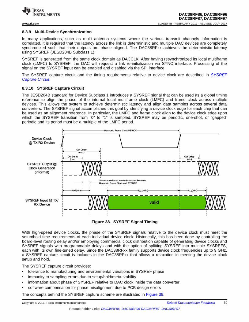
39
DAC38RF86, DAC38RF96DAC38RF87, DAC38RF97
www.ti.com SLASEF4B –FEBRUARY 2017–REVISED JULY 2017
Product Folder Links: DAC38RF86 DAC38RF96 DAC38RF87 DAC38RF97
Submit Documentation FeedbackCopyright © 2017, Texas Instruments Incorporated
8.3.9 Multi-Device SynchronizationIn many applications, such as multi antenna systems where the various transmit channels information iscorrelated, it is required that the latency across the link is deterministic and multiple DAC devices are completelysynchronized such that their outputs are phase aligned. The DAC38RFxx achieves the deterministic latencyusing SYSREF (JESD204B Subclass 1).
SYSREF is generated from the same clock domain as DACCLK. After having resynchronized its local multiframeclock (LMFC) to SYSREF, the DAC will request a link re-initialization via SYNC interface. Processing of thesignal on the SYSREF input can be enabled and disabled via the SPI interface.
The SYSREF capture circuit and the timing requirements relative to device clock are described in SYSREFCapture Circuit.
8.3.10 SYSREF Capture CircuitThe JESD204B standard for Device Subclass 1 introduces a SYSREF signal that can be used as a global timingreference to align the phase of the internal local multiframe clock (LMFC) and frame clock across multipledevices. This allows the system to achieve deterministic latency and align data samples across several dataconverters. The SYSREF signal accomplishes this goal by identifying a device clock edge for each chip that canbe used as an alignment reference. In particular, the LMFC and frame clock align to the device clock edge uponwhich the SYSREF transition from “0” to “1” is sampled. SYSREF may be periodic, one-shot, or “gapped”periodic and its period must be a multiple of the LMFC period.
Figure 38. SYSREF Signal Timing
With high-speed device clocks, the phase of the SYSREF signals relative to the device clock must meet thesetup/hold time requirements of each individual device clock. Historically, this has been done by controlling theboard-level routing delay and/or employing commercial clock distribution capable of generating device clocks andSYSREF signals with programmable delays and with the option of splitting SYSREF into multiple SYSREFS,each with its own fine-tuned delay. Since the DAC38RFxx family supports device clock frequencies up to 9 GHz,a SYSREF capture circuit is includes in the DAC38RFxx that allows a relaxation in meeting the device clocksetup and hold.
The SYSREF capture circuit provides:• tolerance to manufacturing and environmental variations in SYSREF phase• immunity to sampling errors due to setup/hold/meta-stability• information about phase of SYSREF relative to DAC clock inside the data converter• software compensation for phase misalignment due to PCB design errors
The concepts behind the SYSREF capture scheme are illustrated in Figure 39.
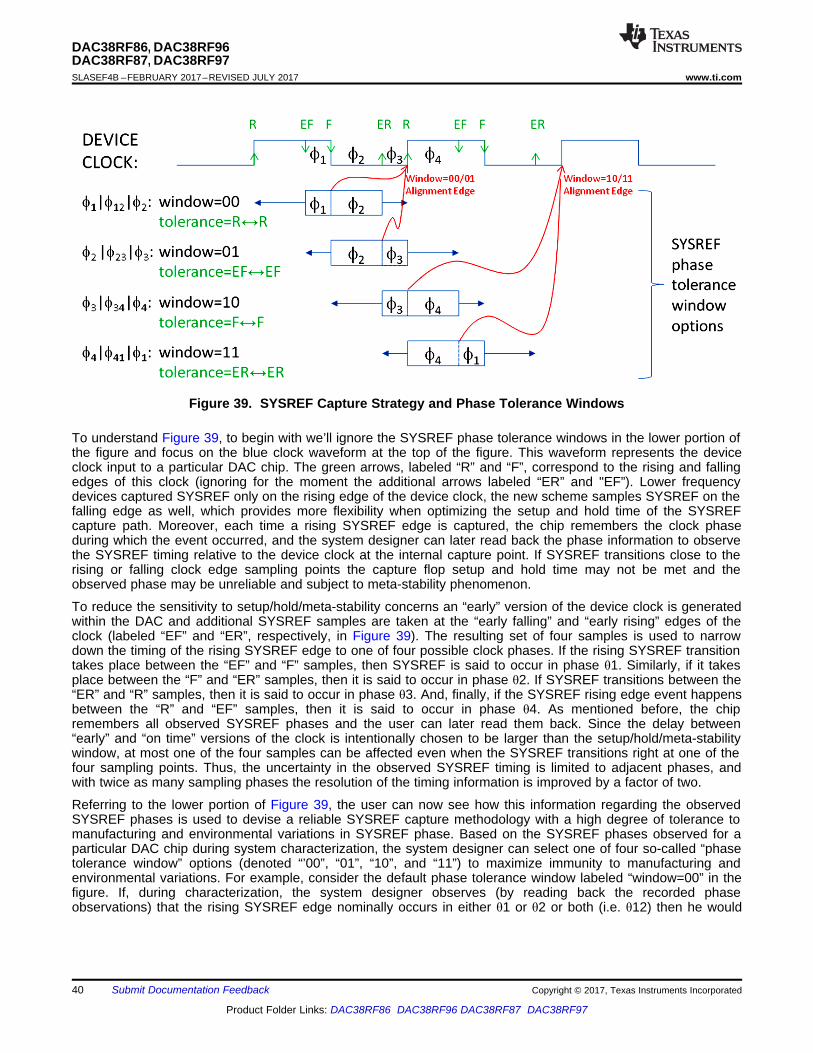
40
DAC38RF86, DAC38RF96DAC38RF87, DAC38RF97SLASEF4B –FEBRUARY 2017–REVISED JULY 2017 www.ti.com
Product Folder Links: DAC38RF86 DAC38RF96 DAC38RF87 DAC38RF97
Submit Documentation Feedback Copyright © 2017, Texas Instruments Incorporated
Figure 39. SYSREF Capture Strategy and Phase Tolerance Windows
To understand Figure 39, to begin with we’ll ignore the SYSREF phase tolerance windows in the lower portion ofthe figure and focus on the blue clock waveform at the top of the figure. This waveform represents the deviceclock input to a particular DAC chip. The green arrows, labeled “R” and “F”, correspond to the rising and fallingedges of this clock (ignoring for the moment the additional arrows labeled “ER” and "EF”). Lower frequencydevices captured SYSREF only on the rising edge of the device clock, the new scheme samples SYSREF on thefalling edge as well, which provides more flexibility when optimizing the setup and hold time of the SYSREFcapture path. Moreover, each time a rising SYSREF edge is captured, the chip remembers the clock phaseduring which the event occurred, and the system designer can later read back the phase information to observethe SYSREF timing relative to the device clock at the internal capture point. If SYSREF transitions close to therising or falling clock edge sampling points the capture flop setup and hold time may not be met and theobserved phase may be unreliable and subject to meta-stability phenomenon.
To reduce the sensitivity to setup/hold/meta-stability concerns an “early” version of the device clock is generatedwithin the DAC and additional SYSREF samples are taken at the “early falling” and “early rising” edges of theclock (labeled “EF” and “ER”, respectively, in Figure 39). The resulting set of four samples is used to narrowdown the timing of the rising SYSREF edge to one of four possible clock phases. If the rising SYSREF transitiontakes place between the “EF” and “F” samples, then SYSREF is said to occur in phase θ1. Similarly, if it takesplace between the “F” and “ER” samples, then it is said to occur in phase θ2. If SYSREF transitions between the“ER” and “R” samples, then it is said to occur in phase θ3. And, finally, if the SYSREF rising edge event happensbetween the “R” and “EF” samples, then it is said to occur in phase θ4. As mentioned before, the chipremembers all observed SYSREF phases and the user can later read them back. Since the delay between“early” and “on time” versions of the clock is intentionally chosen to be larger than the setup/hold/meta-stabilitywindow, at most one of the four samples can be affected even when the SYSREF transitions right at one of thefour sampling points. Thus, the uncertainty in the observed SYSREF timing is limited to adjacent phases, andwith twice as many sampling phases the resolution of the timing information is improved by a factor of two.
Referring to the lower portion of Figure 39, the user can now see how this information regarding the observedSYSREF phases is used to devise a reliable SYSREF capture methodology with a high degree of tolerance tomanufacturing and environmental variations in SYSREF phase. Based on the SYSREF phases observed for aparticular DAC chip during system characterization, the system designer can select one of four so-called “phasetolerance window” options (denoted “’00”, “01”, “10”, and “11”) to maximize immunity to manufacturing andenvironmental variations. For example, consider the default phase tolerance window labeled “window=00” in thefigure. If, during characterization, the system designer observes (by reading back the recorded phaseobservations) that the rising SYSREF edge nominally occurs in either θ1 or θ2 or both (i.e. θ12) then he would
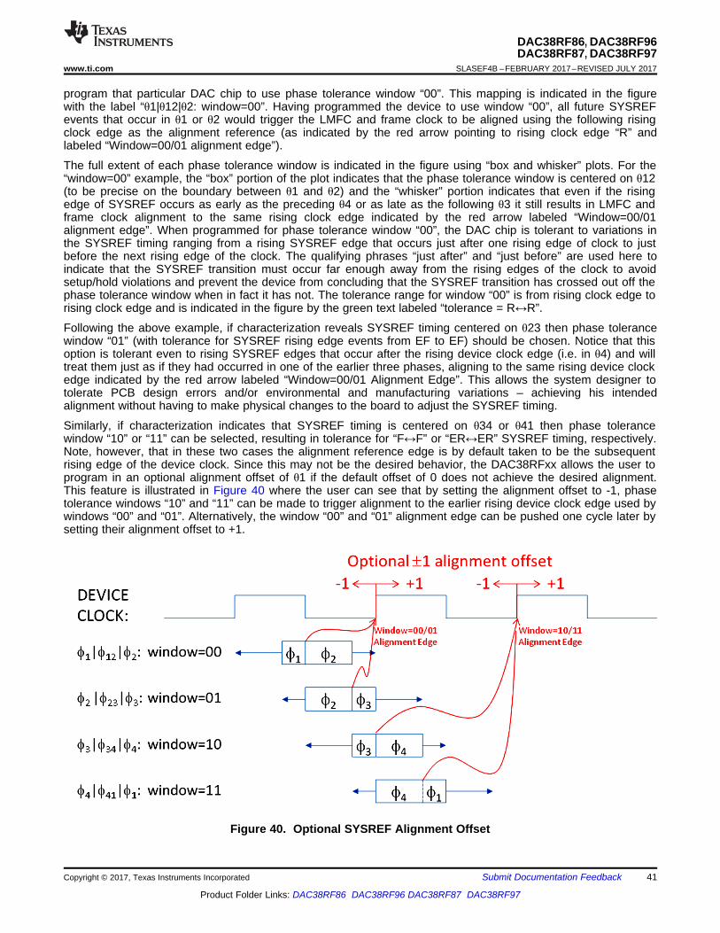
41
DAC38RF86, DAC38RF96DAC38RF87, DAC38RF97
www.ti.com SLASEF4B –FEBRUARY 2017–REVISED JULY 2017
Product Folder Links: DAC38RF86 DAC38RF96 DAC38RF87 DAC38RF97
Submit Documentation FeedbackCopyright © 2017, Texas Instruments Incorporated
program that particular DAC chip to use phase tolerance window “00”. This mapping is indicated in the figurewith the label “θ1|θ12|θ2: window=00”. Having programmed the device to use window “00”, all future SYSREFevents that occur in θ1 or θ2 would trigger the LMFC and frame clock to be aligned using the following risingclock edge as the alignment reference (as indicated by the red arrow pointing to rising clock edge “R” andlabeled “Window=00/01 alignment edge”).
The full extent of each phase tolerance window is indicated in the figure using “box and whisker” plots. For the“window=00” example, the “box” portion of the plot indicates that the phase tolerance window is centered on θ12(to be precise on the boundary between θ1 and θ2) and the “whisker” portion indicates that even if the risingedge of SYSREF occurs as early as the preceding θ4 or as late as the following θ3 it still results in LMFC andframe clock alignment to the same rising clock edge indicated by the red arrow labeled “Window=00/01alignment edge”. When programmed for phase tolerance window “00”, the DAC chip is tolerant to variations inthe SYSREF timing ranging from a rising SYSREF edge that occurs just after one rising edge of clock to justbefore the next rising edge of the clock. The qualifying phrases “just after” and “just before” are used here toindicate that the SYSREF transition must occur far enough away from the rising edges of the clock to avoidsetup/hold violations and prevent the device from concluding that the SYSREF transition has crossed out off thephase tolerance window when in fact it has not. The tolerance range for window “00” is from rising clock edge torising clock edge and is indicated in the figure by the green text labeled “tolerance = R↔R”.
Following the above example, if characterization reveals SYSREF timing centered on θ23 then phase tolerancewindow “01” (with tolerance for SYSREF rising edge events from EF to EF) should be chosen. Notice that thisoption is tolerant even to rising SYSREF edges that occur after the rising device clock edge (i.e. in θ4) and willtreat them just as if they had occurred in one of the earlier three phases, aligning to the same rising device clockedge indicated by the red arrow labeled “Window=00/01 Alignment Edge”. This allows the system designer totolerate PCB design errors and/or environmental and manufacturing variations – achieving his intendedalignment without having to make physical changes to the board to adjust the SYSREF timing.
Similarly, if characterization indicates that SYSREF timing is centered on θ34 or θ41 then phase tolerancewindow “10” or “11” can be selected, resulting in tolerance for “F↔F” or “ER↔ER” SYSREF timing, respectively.Note, however, that in these two cases the alignment reference edge is by default taken to be the subsequentrising edge of the device clock. Since this may not be the desired behavior, the DAC38RFxx allows the user toprogram in an optional alignment offset of θ1 if the default offset of 0 does not achieve the desired alignment.This feature is illustrated in Figure 40 where the user can see that by setting the alignment offset to -1, phasetolerance windows “10” and “11” can be made to trigger alignment to the earlier rising device clock edge used bywindows “00” and “01”. Alternatively, the window “00” and “01” alignment edge can be pushed one cycle later bysetting their alignment offset to +1.
Figure 40. Optional SYSREF Alignment Offset

42
DAC38RF86, DAC38RF96DAC38RF87, DAC38RF97SLASEF4B –FEBRUARY 2017–REVISED JULY 2017 www.ti.com
Product Folder Links: DAC38RF86 DAC38RF96 DAC38RF87 DAC38RF97
Submit Documentation Feedback Copyright © 2017, Texas Instruments Incorporated
Several important controls related to SYSREF alignment and capture timing are contained in registerSYSR_CAPTURE (8.5.78). For example, as mentioned before, the device is capable of monitoring the observedphases of the rising SYSREF edge events; however, in order to avoid unwanted noise coupling from theSYSREF circuits into the DAC output, the SYSREF monitoring circuits are disabled by default. FieldSYSR_STATUS_ENA enables SYSREF status monitoring. Field SYSR_PHASE_WDW contains the the phasetolerance window selected for normal operation, which is optimized during characterization. FieldSYSR_ALIGN_DLY contains the control that allows the system designer to optionally offset the SYSREFalignment event by ±1 device clock cycles. Field SYSR_STATUS_ENA enables the SYSREF capture alignmentaccumulation and will generate alarms when enabled. Writing a “1” to field SYSR_ALIGN_SYNC clears theaccumulated SYSREF alignment statistics. The SYSREF alignment block can be bypassed completely by fieldSYSREF_BYPASS_ALIGN, in which case SYSREF is latched by the rising edge of DACCLK.
When field SYSR_STATUS_ENA is high the device records the phase associated with each SYSREF event foruse in characterizing the SYSREF capture timing and selecting an appropriate phase tolerance window. Thephase data is available in two forms. First, each of the four phases has a corresponding “sticky” alarm flagindicating which phases have been observed since the last time the register was cleared. In addition, the devicealso accumulates statistics on the relative number of occurrences of each phase spanning multiple SYSREFevents using saturating 8-bit counters. These accumulated real-time SYSREF statistics allow us to account fortime-varying effects during characterization such as potential timing differences between the 1st and Nth edgesin a “gapped” SYSREF pulse train. The counters are fields PHASE1_CNT and PHASE2_CNT in registerSYSREF12_CNT (8.5.10), PHASE3_CNT and PHASE4_CNT in register SYSREF34_CNT (8.5.11), andALIGN_TO_R1_CNT and ALIGN_TO_R3_CNT in register SYSREF_ALIGN_R (8.5.9).
The accumulated SYSREF statistics can be cleared by writing ‘1’ to SYSR_ALIGN_SYNC. This sync signalaffects only the SYSREF statistics monitors and does not cause a sync of any other portions of the design.Before collecting phase statistics, the user must first enable the SYSREF status monitoring logic by setting theSYSR_STATUS_ENA bit. The user must then generate a repeating SYSREF input before usingSYSR_ALIGN_SYNC to clear the statistic counters. This is necessary to flush invalid data out of the statuspipeline.
The “sticky” alarm flags indicating which of the four phases have been observed since the lastSYSR_ALIGN_SYNC write of ‘1’ are fields ALM_SYSRPHASE1 to ALM_SYSRPHASE4 and are contained in theALM_SYSREF_DET register (8.5.6).
8.3.11 JESD204B Subclass 0 supportSome functionality has been implemented to support Subclass 0 operation. Note that programming theSUBCLASSV configuration parameter has no functional impact on the logic. The value programmed forSUBCLASSV is only used in the initial lane alignment (ILA) sequence. The following configuration parametersare used to support Subclass 0 operation:• Field SYSREF_MODE in register JESD_SYSR_MODE (8.5.56) = 0• Field DISABLE_ERR_RPT in register JESD_ERR_OUT (8.5.53) = 1• Field MIN_LATENCY_ENA in register JESD_MATCH (8.5.50) = 1
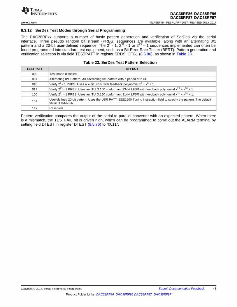
43
DAC38RF86, DAC38RF96DAC38RF87, DAC38RF97
www.ti.com SLASEF4B –FEBRUARY 2017–REVISED JULY 2017
Product Folder Links: DAC38RF86 DAC38RF96 DAC38RF87 DAC38RF97
Submit Documentation FeedbackCopyright © 2017, Texas Instruments Incorporated
8.3.12 SerDes Test Modes through Serial ProgrammingThe DAC38RFxx supports a number of basic pattern generation and verification of SerDes via the serialinterface. Three pseudo random bit stream (PRBS) sequences are available, along with an alternating 0/1pattern and a 20-bit user-defined sequence. The 27 - 1, 231 - 1 or 223 – 1 sequences implemented can often befound programmed into standard test equipment, such as a Bit Error Rate Tester (BERT). Pattern generation andverification selection is via field TESTPATT in register SRDS_CFG1 (8.5.86), as shown in Table 23.
Table 23. SerDes Test Pattern SelectionTESTPATT EFFECT
000 Test mode disabled.001 Alternating 0/1 Pattern. An alternating 0/1 pattern with a period of 2 UI.010 Verify 27 - 1 PRBS. Uses a 7-bit LFSR with feedback polynomial x7 + x6 + 1.011 Verify 223 - 1 PRBS. Uses an ITU O.150 conformant 23-bit LFSR with feedback polynomial x23 + x18 + 1.100 Verify 231 - 1 PRBS. Uses an ITU O.150 conformant 31-bit LFSR with feedback polynomial x31 + x28 + 1.
101 User-defined 20-bit pattern. Uses the USR PATT IEEE1500 Tuning instruction field to specify the pattern. The defaultvalue is 0x66666.
11x Reserved.
Pattern verification compares the output of the serial to parallel converter with an expected pattern. When thereis a mismatch, the TESTFAIL bit is driven high, which can be programmed to come out the ALARM terminal bysetting field DTEST in register DTEST (8.5.76) to “0011”.
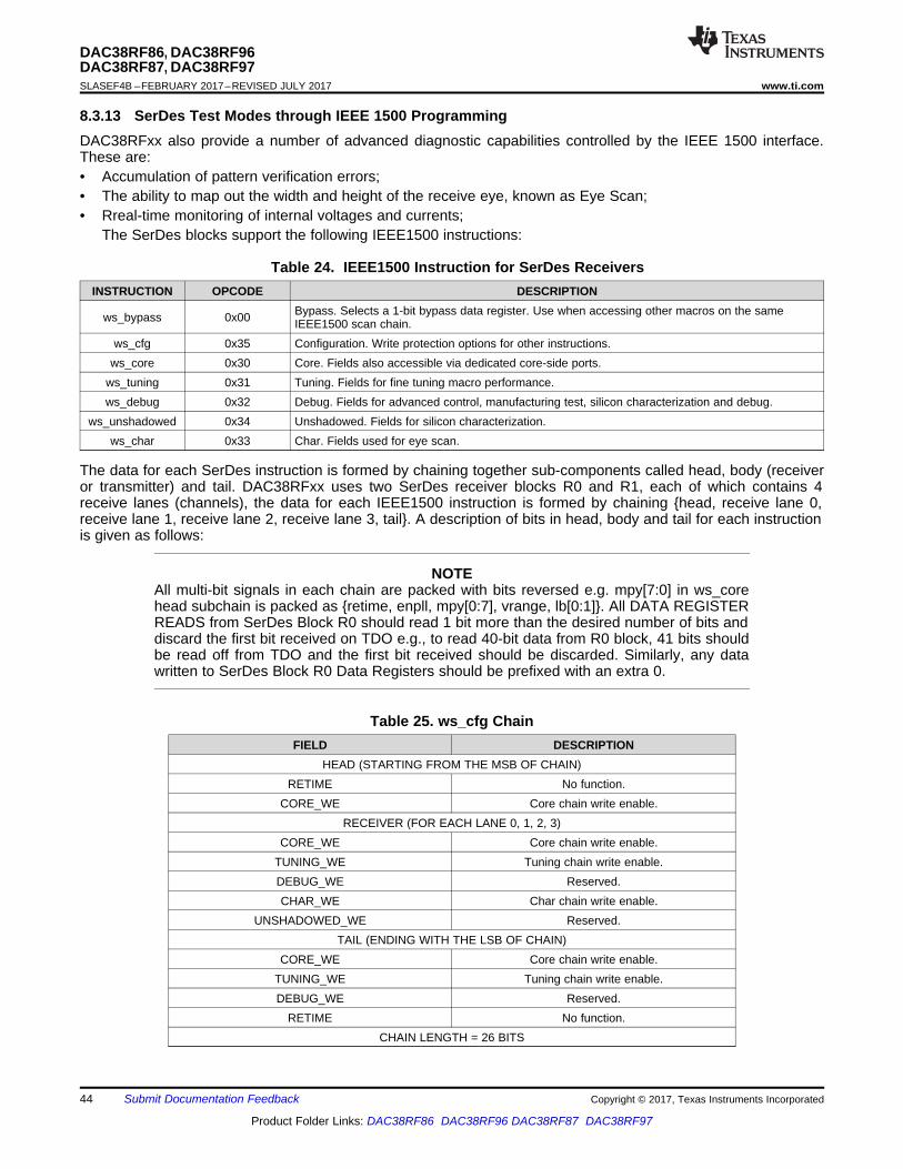
44
DAC38RF86, DAC38RF96DAC38RF87, DAC38RF97SLASEF4B –FEBRUARY 2017–REVISED JULY 2017 www.ti.com
Product Folder Links: DAC38RF86 DAC38RF96 DAC38RF87 DAC38RF97
Submit Documentation Feedback Copyright © 2017, Texas Instruments Incorporated
8.3.13 SerDes Test Modes through IEEE 1500 ProgrammingDAC38RFxx also provide a number of advanced diagnostic capabilities controlled by the IEEE 1500 interface.These are:• Accumulation of pattern verification errors;• The ability to map out the width and height of the receive eye, known as Eye Scan;• Rreal-time monitoring of internal voltages and currents;
The SerDes blocks support the following IEEE1500 instructions:
Table 24. IEEE1500 Instruction for SerDes ReceiversINSTRUCTION OPCODE DESCRIPTION
ws_bypass 0x00 Bypass. Selects a 1-bit bypass data register. Use when accessing other macros on the sameIEEE1500 scan chain.
ws_cfg 0x35 Configuration. Write protection options for other instructions.ws_core 0x30 Core. Fields also accessible via dedicated core-side ports.
ws_tuning 0x31 Tuning. Fields for fine tuning macro performance.ws_debug 0x32 Debug. Fields for advanced control, manufacturing test, silicon characterization and debug.
ws_unshadowed 0x34 Unshadowed. Fields for silicon characterization.ws_char 0x33 Char. Fields used for eye scan.
The data for each SerDes instruction is formed by chaining together sub-components called head, body (receiveror transmitter) and tail. DAC38RFxx uses two SerDes receiver blocks R0 and R1, each of which contains 4receive lanes (channels), the data for each IEEE1500 instruction is formed by chaining {head, receive lane 0,receive lane 1, receive lane 2, receive lane 3, tail}. A description of bits in head, body and tail for each instructionis given as follows:
NOTEAll multi-bit signals in each chain are packed with bits reversed e.g. mpy[7:0] in ws_corehead subchain is packed as {retime, enpll, mpy[0:7], vrange, lb[0:1]}. All DATA REGISTERREADS from SerDes Block R0 should read 1 bit more than the desired number of bits anddiscard the first bit received on TDO e.g., to read 40-bit data from R0 block, 41 bits shouldbe read off from TDO and the first bit received should be discarded. Similarly, any datawritten to SerDes Block R0 Data Registers should be prefixed with an extra 0.
Table 25. ws_cfg ChainFIELD DESCRIPTION
HEAD (STARTING FROM THE MSB OF CHAIN)RETIME No function.
CORE_WE Core chain write enable.RECEIVER (FOR EACH LANE 0, 1, 2, 3)
CORE_WE Core chain write enable.TUNING_WE Tuning chain write enable.DEBUG_WE Reserved.CHAR_WE Char chain write enable.
UNSHADOWED_WE Reserved.TAIL (ENDING WITH THE LSB OF CHAIN)
CORE_WE Core chain write enable.TUNING_WE Tuning chain write enable.DEBUG_WE Reserved.
RETIME No function.CHAIN LENGTH = 26 BITS
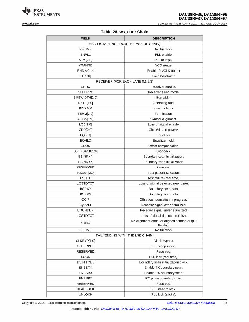
45
DAC38RF86, DAC38RF96DAC38RF87, DAC38RF97
www.ti.com SLASEF4B –FEBRUARY 2017–REVISED JULY 2017
Product Folder Links: DAC38RF86 DAC38RF96 DAC38RF87 DAC38RF97
Submit Documentation FeedbackCopyright © 2017, Texas Instruments Incorporated
Table 26. ws_core ChainFIELD DESCRIPTION
HEAD (STARTING FROM THE MSB OF CHAIN)RETIME No function.ENPLL PLL enable.
MPY[7:0] PLL multiply.VRANGE VCO range.
ENDIVCLK Enable DIVCLK outputLB[1:0] Loop bandwidth
RECEIVER (FOR EACH LANE 0,1,2,3)ENRX Receiver enable.
SLEEPRX Receiver sleep mode.BUSWIDTH[2:0] Bus width.
RATE[1:0] Operating rate.INVPAIR Invert polarity.
TERM[2:0] Termination.ALIGN[1:0] Symbol alignment.LOS[2:0] Loss of signal enable.CDR[2:0] Clock/data recovery.EQ[2:0] Equalizer.EQHLD Equalizer hold.ENOC Offset compensation.
LOOPBACK[1:0] Loopback.BSINRXP Boundary scan initialization.BSINRXN Boundary scan initialization.
RESERVED Reserved.Testpatt[2:0] Test pattern selection.TESTFAIL Test failure (real time).
LOSTDTCT Loss of signal detected (real time).BSRXP Boundary scan data.BSRXN Boundary scan data.OCIP Offset compensation in progress.
EQOVER Receiver signal over equalized.EQUNDER Receiver signal under equalized.LOSTDTCT Loss of signal detected (sticky).
SYNC Re-alignment done, or aligned comma output(sticky).
RETIME No function.TAIL (ENDING WITH THE LSB CHAIN)
CLKBYP[1:0] Clock bypass.SLEEPPLL PLL sleep mode.RESERVED Reserved.
LOCK PLL lock (real time).BSINITCLK Boundary scan initialization clock.
ENBSTX Enable TX boundary scan.ENBSRX Enable RX boundary scan.ENBSPT RX pulse boundary scan.
RESERVED Reserved.NEARLOCK PLL near to lock.
UNLOCK PLL lock (sticky).
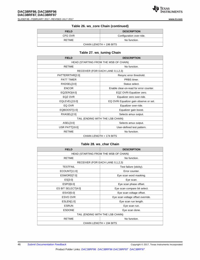
46
DAC38RF86, DAC38RF96DAC38RF87, DAC38RF97SLASEF4B –FEBRUARY 2017–REVISED JULY 2017 www.ti.com
Product Folder Links: DAC38RF86 DAC38RF96 DAC38RF87 DAC38RF97
Submit Documentation Feedback Copyright © 2017, Texas Instruments Incorporated
Table 26. ws_core Chain (continued)FIELD DESCRIPTION
CFG OVR Configuration over-ride.RETIME No function.
CHAIN LENGTH = 196 BITS
Table 27. ws_tuning ChainFIELD DESCRIPTION
HEAD (STARTING FROM THE MSB OF CHAIN)RETIME No function.
RECEIVER (FOR EACH LANE 0,1,2,3)PATTERRTHR[2:0] Resync error threshold.
PATT TIMER PRBS timer.RXDSEL[3:0] Status select.
ENCOR Enable clear-on-read for error counter.EQZERO[4:0] EQZ OVRi Equalizer zero.
EQZ OVR Equalizer zero over-ride.EQLEVEL[15:0] EQ OVRi Equalizer gain observe or set.
EQ OVR Equalizer over-ride.EQBOOST[1:0] Equalizer gain boost.RXASEL[2:0] Selects amux output.
TAIL (ENDING WITH THE LSB CHAIN)ASEL[3:0] Selects amux output.
USR PATT[19:0] User-defined test pattern.RETIME No function.
CHAIN LENGTH = 174 BITS
Table 28. ws_char ChainFIELD DESCRIPTION
HEAD (STARTING FROM THE MSB OF CHAIN)RETIME No function.
RECEIVER (FOR EACH LANE 0,1,2,3)TESTFAIL Test failure (sticky).
ECOUNT[11:0] Error counter.ESWORD[7:0] Eye scan word masking.
ES[3:0] Eye scan.ESPO[6:0] Eye scan phase offset.
ES BIT SELECT[4:0] Eye scan compare bit select.ESVO[5:0] Eye scan voltage offset.ESVO OVR Eye scan voltage offset override.ESLEN[1:0] Eye scan run length.
ESRUN Eye scan run.ESDONE Eye scan done.
TAIL (ENDING WITH THE LSB CHAIN)RETIME No function.
CHAIN LENGTH = 194 BITS
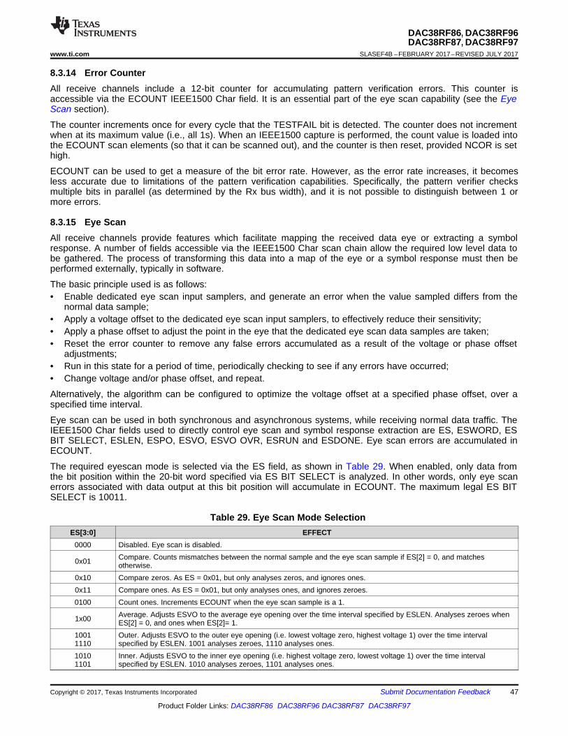
47
DAC38RF86, DAC38RF96DAC38RF87, DAC38RF97
www.ti.com SLASEF4B –FEBRUARY 2017–REVISED JULY 2017
Product Folder Links: DAC38RF86 DAC38RF96 DAC38RF87 DAC38RF97
Submit Documentation FeedbackCopyright © 2017, Texas Instruments Incorporated
8.3.14 Error CounterAll receive channels include a 12-bit counter for accumulating pattern verification errors. This counter isaccessible via the ECOUNT IEEE1500 Char field. It is an essential part of the eye scan capability (see the EyeScan section).
The counter increments once for every cycle that the TESTFAIL bit is detected. The counter does not incrementwhen at its maximum value (i.e., all 1s). When an IEEE1500 capture is performed, the count value is loaded intothe ECOUNT scan elements (so that it can be scanned out), and the counter is then reset, provided NCOR is sethigh.
ECOUNT can be used to get a measure of the bit error rate. However, as the error rate increases, it becomesless accurate due to limitations of the pattern verification capabilities. Specifically, the pattern verifier checksmultiple bits in parallel (as determined by the Rx bus width), and it is not possible to distinguish between 1 ormore errors.
8.3.15 Eye ScanAll receive channels provide features which facilitate mapping the received data eye or extracting a symbolresponse. A number of fields accessible via the IEEE1500 Char scan chain allow the required low level data tobe gathered. The process of transforming this data into a map of the eye or a symbol response must then beperformed externally, typically in software.
The basic principle used is as follows:• Enable dedicated eye scan input samplers, and generate an error when the value sampled differs from the
normal data sample;• Apply a voltage offset to the dedicated eye scan input samplers, to effectively reduce their sensitivity;• Apply a phase offset to adjust the point in the eye that the dedicated eye scan data samples are taken;• Reset the error counter to remove any false errors accumulated as a result of the voltage or phase offset
adjustments;• Run in this state for a period of time, periodically checking to see if any errors have occurred;• Change voltage and/or phase offset, and repeat.
Alternatively, the algorithm can be configured to optimize the voltage offset at a specified phase offset, over aspecified time interval.
Eye scan can be used in both synchronous and asynchronous systems, while receiving normal data traffic. TheIEEE1500 Char fields used to directly control eye scan and symbol response extraction are ES, ESWORD, ESBIT SELECT, ESLEN, ESPO, ESVO, ESVO OVR, ESRUN and ESDONE. Eye scan errors are accumulated inECOUNT.
The required eyescan mode is selected via the ES field, as shown in Table 29. When enabled, only data fromthe bit position within the 20-bit word specified via ES BIT SELECT is analyzed. In other words, only eye scanerrors associated with data output at this bit position will accumulate in ECOUNT. The maximum legal ES BITSELECT is 10011.
Table 29. Eye Scan Mode SelectionES[3:0] EFFECT
0000 Disabled. Eye scan is disabled.
0x01 Compare. Counts mismatches between the normal sample and the eye scan sample if ES[2] = 0, and matchesotherwise.
0x10 Compare zeros. As ES = 0x01, but only analyses zeros, and ignores ones.0x11 Compare ones. As ES = 0x01, but only analyses ones, and ignores zeroes.0100 Count ones. Increments ECOUNT when the eye scan sample is a 1.
1x00 Average. Adjusts ESVO to the average eye opening over the time interval specified by ESLEN. Analyses zeroes whenES[2] = 0, and ones when ES[2]= 1.
10011110
Outer. Adjusts ESVO to the outer eye opening (i.e. lowest voltage zero, highest voltage 1) over the time intervalspecified by ESLEN. 1001 analyses zeroes, 1110 analyses ones.
10101101
Inner. Adjusts ESVO to the inner eye opening (i.e. highest voltage zero, lowest voltage 1) over the time intervalspecified by ESLEN. 1010 analyses zeroes, 1101 analyses ones.
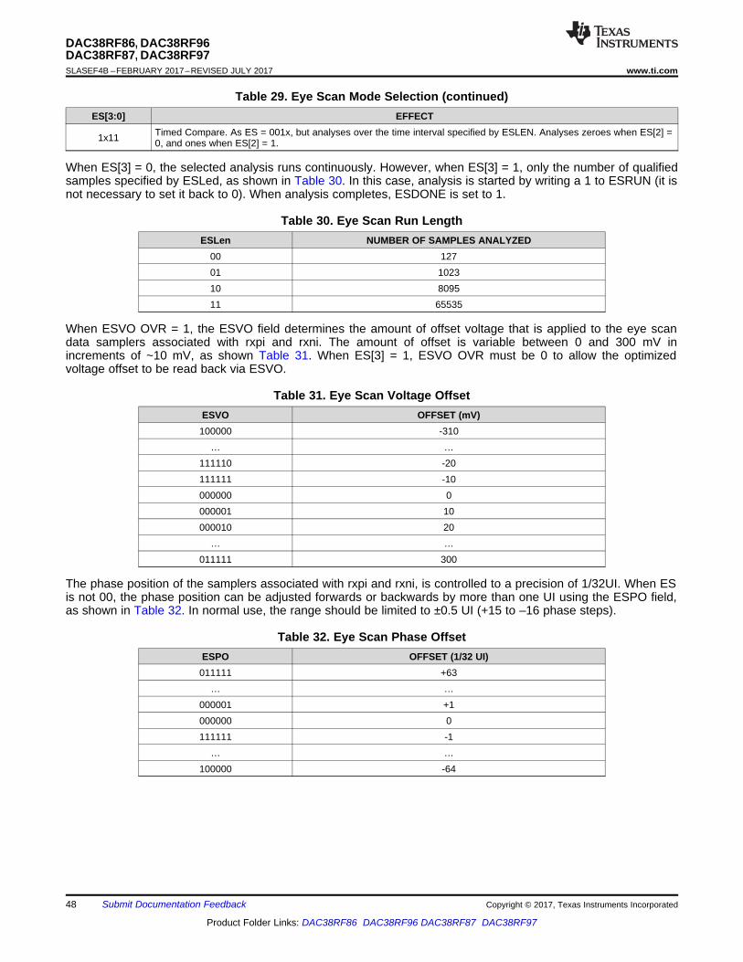
48
DAC38RF86, DAC38RF96DAC38RF87, DAC38RF97SLASEF4B –FEBRUARY 2017–REVISED JULY 2017 www.ti.com
Product Folder Links: DAC38RF86 DAC38RF96 DAC38RF87 DAC38RF97
Submit Documentation Feedback Copyright © 2017, Texas Instruments Incorporated
Table 29. Eye Scan Mode Selection (continued)ES[3:0] EFFECT
1x11 Timed Compare. As ES = 001x, but analyses over the time interval specified by ESLEN. Analyses zeroes when ES[2] =0, and ones when ES[2] = 1.
When ES[3] = 0, the selected analysis runs continuously. However, when ES[3] = 1, only the number of qualifiedsamples specified by ESLed, as shown in Table 30. In this case, analysis is started by writing a 1 to ESRUN (it isnot necessary to set it back to 0). When analysis completes, ESDONE is set to 1.
Table 30. Eye Scan Run LengthESLen NUMBER OF SAMPLES ANALYZED
00 12701 102310 809511 65535
When ESVO OVR = 1, the ESVO field determines the amount of offset voltage that is applied to the eye scandata samplers associated with rxpi and rxni. The amount of offset is variable between 0 and 300 mV inincrements of ~10 mV, as shown Table 31. When ES[3] = 1, ESVO OVR must be 0 to allow the optimizedvoltage offset to be read back via ESVO.
Table 31. Eye Scan Voltage OffsetESVO OFFSET (mV)100000 -310
… …111110 -20111111 -10000000 0000001 10000010 20
… …011111 300
The phase position of the samplers associated with rxpi and rxni, is controlled to a precision of 1/32UI. When ESis not 00, the phase position can be adjusted forwards or backwards by more than one UI using the ESPO field,as shown in Table 32. In normal use, the range should be limited to ±0.5 UI (+15 to –16 phase steps).
Table 32. Eye Scan Phase OffsetESPO OFFSET (1/32 UI)011111 +63
… …000001 +1000000 0111111 -1
… …100000 -64

49
DAC38RF86, DAC38RF96DAC38RF87, DAC38RF97
www.ti.com SLASEF4B –FEBRUARY 2017–REVISED JULY 2017
Product Folder Links: DAC38RF86 DAC38RF96 DAC38RF87 DAC38RF97
Submit Documentation FeedbackCopyright © 2017, Texas Instruments Incorporated
8.3.16 JESD204B Pattern TestThe DAC38RFxx supports the following test patterns for JESD204B:• Link layer test pattern by setting field JESD_TEST_SEQ in register JESD_LN_EN (8.5.45) and monitoring the
lane alarms (1 = fail, 0 = pass)– Verify repeating /D.21.5/ high frequency pattern for random jitter (RJ)– Verify repeating /K.28.5/ mixed frequency pattern for deterministic jitter (DJ)– Verify repeating initial lane alignment (ILA) sequence
• RPAT, JSPAT or JTSPAT pattern can be verified using errors counter of 8b/10b errors produced over anamount of time to get an estimate of BER.
• Transport layer test pattern: implements a short transport layer pattern check based on F = 1, 2, 4 or 8. Theshort test pattern has a duration of one frame period and is repeated continuously for the duration of the test.Each sample has a unique value that can be identified with the position of the sample in the user data format.The sample values are such that correct sample values will never be decoded at the receiver if there is amismatch between the mapping formats being used at the transmitter and receiver devices. This cangenerally be accomplished by ensuring there are no repeating sub patterns within the stream of samplesbeing transmitted. Refer to the JESD204B standard section 5.1.6 for more details.
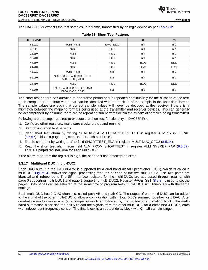
50
DAC38RF86, DAC38RF96DAC38RF87, DAC38RF97SLASEF4B –FEBRUARY 2017–REVISED JULY 2017 www.ti.com
Product Folder Links: DAC38RF86 DAC38RF96 DAC38RF87 DAC38RF97
Submit Documentation Feedback Copyright © 2017, Texas Instruments Incorporated
The DAC38RFxx expects the test samples, in a frame, transmitted by an logic device as per Table 33:
Table 33. Short Test PatternsJESD Mode i0 q0 i1 q1
82121 7CB8, F431 6DA9, E520 n/a n/a42111 7CB8 F431 n/a n/a22210 7CB8 F431 n/a n/a12410 7CB8 F431 n/a n/a44210 7CB8 F431 6DA9 E52024410 7CB8 F431 6DA9 E52041121 7CB8, F431 n/a n/a n/a
81180 7C00, B800, F400, 3100, 6D00,A900, E500, 2000 n/a n/a n/a
24310 7CB0 F430 6DA0 E520
41380 7CB0, F430, 6DA0, E520, F870,E960, DA50, CB40 n/a n/a n/a
The short test pattern has duration of one frame period and is repeated continuously for the duration of the test.Each sample has a unique value that can be identified with the position of the sample in the user data format.The sample values are such that correct sample values will never be decoded at the receiver if there is amismatch between the mapping formats being used at the transmitter and receiver devices. This can generallybe accomplished by ensuring there are no repeating sub patterns within the stream of samples being transmitted.
Following are the steps required to execute the short test functionality in DAC38RFxx.1. Configure other registers, make sure clocks are up and running.2. Start driving short test patterns3. Clear short test alarm by writing ‘0’ to field ALM_FROM_SHORTTEST in register ALM_SYSREF_PAP
(8.5.67). This is a paged register, one for each Multi-DUC.4. Enable short test by writing a ‘1’ to field SHORTTEST_ENA in register MULTIDUC_CFG2 (8.5.14).5. Read the short test alarm from field ALM_FROM_SHORTTEST in register ALM_SYSREF_PAP (8.5.67).
This is a paged register, one for each Multi-DUC
If the alarm read from the register is high, the short test has detected an error.
8.3.17 Multiband DUC (multi-DUC)Each DAC output in the DAC38RFxx is supported by a dual band digital upconverter (DUC), which is called amulti-DUC.Figure 41 shows the signal processing features of each of the two multi-DUCs. The two paths areidentical and independent. The SPI interface registers for the multi-DUCs are addressed through paging, withpage 0 supporting multi-DUC1 and page 1 supporting multi-DUC2. Register PAGE_SET (8.5.8) is used to set thepages. Both pages can be selected at the same time to program both multi-DUCs simultaneously with the samesettings.
Each multi-DUC has 2 DUC channels, called path AB and path CD. The output of one multi-DUC can be addedto the signal of the other multi-DUC to allow a configuration with 4 total DUCs summed together for 1 DAC. Afterquadrature modulation is a sin(x)/x compensation filter, followed by the multiband summation block. The multi-band summation block had the ability to add the signals from the other multi-DUC for a combined 4 DUCs, eachwith independent frequency control. The final block is an output delay block with 0 – 15 sample range.
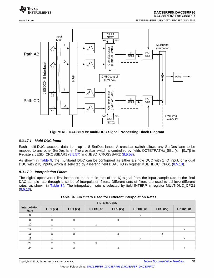
16
16
Com
plex
Mix
er(F
MIX
or
CM
IX)
JES
D20
4B In
terf
ace
16
16xN
xN
xN
xN
xsin(x)
Com
plex
Mix
er(F
MIX
or
CM
IX)
48-bit NCO2
cos sin
48-bit NCO1
cos sin
CMIX control(±n*Fs/4)
InputMux
Multibandsummation
xsin(x)
PAPGain
PAPGain
PA
P
From 2nd multi-DUC
Delay
I
Q
I
Q
Path AB
Path CD
51
DAC38RF86, DAC38RF96DAC38RF87, DAC38RF97
www.ti.com SLASEF4B –FEBRUARY 2017–REVISED JULY 2017
Product Folder Links: DAC38RF86 DAC38RF96 DAC38RF87 DAC38RF97
Submit Documentation FeedbackCopyright © 2017, Texas Instruments Incorporated
Figure 41. DAC38RFxx multi-DUC Signal Processing Block Diagram
8.3.17.1 Multi-DUC inputEach multi-DUC, accepts data from up to 8 SerDes lanes. A crossbar switch allows any SerDes lane to bemapped to any other SerDes lane. The crossbar switch is controlled by fields OCTETPATHx_SEL (x = [0..7]) inRegisters JESD_CROSSBAR1 (8.5.57) and JESD_CROSSBAR2 (8.5.58).
As shown in Table 9, the multiband DUC can be configured as either a single DUC with 1 IQ input, or a dualDUC with 2 IQ inputs, which is selected by asserting field DUAL_IQ in register MULTIDUC_CFG1 (8.5.13).
8.3.17.2 Interpolation FiltersThe digital upconverter first increases the sample rate of the IQ signal from the input sample rate to the finalDAC sample rate through a series of interpolation filters. Different sets of filters are used to achieve differentrates, as shown in Table 34. The interpolation rate is selected by field INTERP in register MULTIDUC_CFG1(8.5.13).
Table 34. FIR filters Used for Different Interpolation RatesFILTERS USED
InterpolationRate FIR0 (2x) FIR1 (2x) LPFIR0_5X FIR2 (2x) LPFIR0_3X FIR3 (2x) LPFIR1_3X
6 x x8 x x x10 x x12 x x x16 x x x x18 x x x20 x x x24 x x x x
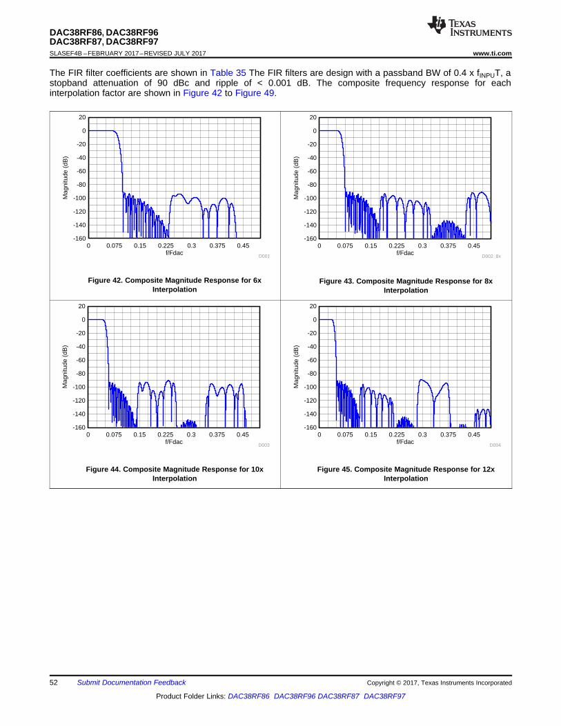
f/Fdac
Mag
nitu
de (
dB)
0 0.075 0.15 0.225 0.3 0.375 0.45-160
-140
-120
-100
-80
-60
-40
-20
0
20
D003f/Fdac
Mag
nitu
de (
dB)
0 0.075 0.15 0.225 0.3 0.375 0.45-160
-140
-120
-100
-80
-60
-40
-20
0
20
D004
f/Fdac
Mag
nitu
de (
dB)
0 0.075 0.15 0.225 0.3 0.375 0.45-160
-140
-120
-100
-80
-60
-40
-20
0
20
D002_8xf/Fdac
Mag
nitu
de (
dB)
0 0.075 0.15 0.225 0.3 0.375 0.45-160
-140
-120
-100
-80
-60
-40
-20
0
20
D001
52
DAC38RF86, DAC38RF96DAC38RF87, DAC38RF97SLASEF4B –FEBRUARY 2017–REVISED JULY 2017 www.ti.com
Product Folder Links: DAC38RF86 DAC38RF96 DAC38RF87 DAC38RF97
Submit Documentation Feedback Copyright © 2017, Texas Instruments Incorporated
The FIR filter coefficients are shown in Table 35 The FIR filters are design with a passband BW of 0.4 x fINPUT, astopband attenuation of 90 dBc and ripple of < 0.001 dB. The composite frequency response for eachinterpolation factor are shown in Figure 42 to Figure 49.
Figure 42. Composite Magnitude Response for 6xInterpolation
Figure 43. Composite Magnitude Response for 8xInterpolation
Figure 44. Composite Magnitude Response for 10xInterpolation
Figure 45. Composite Magnitude Response for 12xInterpolation
f/Fdac
Mag
nitu
de (
dB)
0 0.075 0.15 0.225 0.3 0.375 0.45-160
-140
-120
-100
-80
-60
-40
-20
0
20
D007f/Fdac
Mag
nitu
de (
dB)
0 0.075 0.15 0.225 0.3 0.375 0.45-160
-140
-120
-100
-80
-60
-40
-20
0
20
D001
f/Fdac
Mag
nitu
de (
dB)
0 0.075 0.15 0.225 0.3 0.375 0.45-160
-140
-120
-100
-80
-60
-40
-20
0
20
D005f/Fdac
Mag
nitu
de (
dB)
0 0.075 0.15 0.225 0.3 0.375 0.45-160
-140
-120
-100
-80
-60
-40
-20
0
20
D006
53
DAC38RF86, DAC38RF96DAC38RF87, DAC38RF97
www.ti.com SLASEF4B –FEBRUARY 2017–REVISED JULY 2017
Product Folder Links: DAC38RF86 DAC38RF96 DAC38RF87 DAC38RF97
Submit Documentation FeedbackCopyright © 2017, Texas Instruments Incorporated
Figure 46. Composite Magnitude Response for 16xInterpolation
Figure 47. Composite Magnitude Response for 18xInterpolation
Figure 48. Composite Magnitude Response for 20xInterpolation
Figure 49. Composite Magnitude Response for 24xInterpolation
Table 35. FIR Filter Coefficientstap FIR0 FIR1 LPFIR0_5X FIR2 LPFIR0_3X FIR3 LPFIR1_3X INVSINC
1 6 -12 -6 29 -14 3 25 1
2 0 0 -22 0 -61 0 88 -4
3 -19 84 -51 -214 -125 -25 22 13
4 0 0 -89 0 -95 0 -576 -50
5 47 -336 -117 1209 181 150 -1764 592
6 0 0 -106 2048 681 256 -2263 -50
7 -100 1006 -18 1209 972 150 491 13
8 0 0 171 0 347 0 8139 -4
9 192 -2691 449 -214 -1475 -25 18625 1
10 0 0 745 0 -3519 0 26365
11 -342 10141 930 29 -3528 3 26365
12 0 16384 841 707 18625
13 572 10141 338 9337 8139
14 0 0 -618 19445 491
15 -914 -2691 -1892 26299 -2263
16 0 0 -3147 26299 -1764
17 1409 1006 -3872 19445 -576
54
DAC38RF86, DAC38RF96DAC38RF87, DAC38RF97SLASEF4B –FEBRUARY 2017–REVISED JULY 2017 www.ti.com
Product Folder Links: DAC38RF86 DAC38RF96 DAC38RF87 DAC38RF97
Submit Documentation Feedback Copyright © 2017, Texas Instruments Incorporated
Table 35. FIR Filter Coefficients (continued)tap FIR0 FIR1 LPFIR0_5X FIR2 LPFIR0_3X FIR3 LPFIR1_3X INVSINC
18 0 0 -3500 9337 22
19 -2119 -336 -1564 707 88
20 0 0 2121 -3528 25
21 3152 84 7336 -3519
22 0 0 13430 -1475
23 -4729 -12 19426 347
24 0 24231 972
25 7420 26904 681
26 0 26904 181
27 -13334 24231 -95
28 0 19426 -125
29 41527 13430 -61
30 65536 7336 -14
31 41527 2121
32 0 -1564
33 -13334 -3500
34 0 -3872
35 7420 -3147
36 0 -1892
37 -4729 -618
38 0 338
39 3152 841
40 0 930
41 -2119 745
42 0 449
43 1409 171
44 0 -18
45 -914 -106
46 0 -117
47 572 -89
48 0 -51
49 -342 -22
50 0 -6
51 192
52 0
53 -100
54 0
55 47
56 0
57 -19
58 0
59 6
55
DAC38RF86, DAC38RF96DAC38RF87, DAC38RF97
www.ti.com SLASEF4B –FEBRUARY 2017–REVISED JULY 2017
Product Folder Links: DAC38RF86 DAC38RF96 DAC38RF87 DAC38RF97
Submit Documentation FeedbackCopyright © 2017, Texas Instruments Incorporated
8.3.17.3 JESD204B Modes, Interpolation and Clock phase ProgrammingTable 36 lists the register field values required for each JESD204B mode, interpolation mode and clock phase.The register field addresses are listed in Table 37.
Table 36. Register Programming for JESD and Interpolation ModeMode Register Field Programming
L-M-F-S-Hd
1 TX/2TXInter
pCLOCKPHASES(1-0)
INTERP(4-0)
CLKJESD_DIV
(3-0)
CLKJESD_OUT_DIV(3-0)
L_M1(4-0)
F_M1(7-0)
M_M1(7-0)
S_M1(4-0) HD
N_M1/N’_M1
(4-0)
82121/NA
6 11 00011 0110 0011
00111 0x00 0x01 00001 1 011118 11 00100 0111 0100
12 11 00110 1010 0110
16 11 01000 1011 0111
42111/84111
6 10 00011 0010 0011
00011 0x00 0x01 00000 1 01111
8 11 00100 0011 0100
10 11 00101 0101 0101
12 11 00110 0110 0110
16 11 01000 0111 0111
18 11 01001 1001 1000
24 11 01100 1010 1010
22210/44210
8 01 00100 0001 0100
00001 0x01 0x01 00000 0 01111
12 10 00110 0010 0110
16 11 01000 0011 0111
18 11 01001 0100 1000
20 11 01010 0101 1001
24 11 01100 0110 1010
12410/24410
16 01 01000 0001 011100000 0x03 0x01 00000 0 01111
24 10 00110 0110 1010
44210/88210
8 01 00100 0001 0100
00011 0x01 0x03 00000 0 0111112 10 00110 0010 0110
16 11 01000 0011 0111
24 11 01100 0110 1010
24410/48410
16 01 01000 0001 011100001 0x03 0x03 00000 0 01111
24 10 01100 0010 1010
24310/48310 24 11 01100 0011 1010 00001 0x02 0x03 00000 0 01011
Table 37. Register Field Addresses for JESD204B Modes, Interpolation and Clock Phase ProgrammingRegister Field Name Register Register Address Bit(s) Hyperlink
INTERP MULTIDUC_CFG1 0x0A 12-8 8.5.13CLKJESD_DIV
SerDes_CLK 0x2515-12
8.5.28CLKJESD_OUT_DIV 11-8
L_M1 JESD_K_L 0x4C 4-0 8.5.47F_M1 JESD_RBD_F 0x4B 7-0 8.5.46M_M1
JESD_M_S 0x4D15-8
8.5.48S_M1 4-0
HDJESD_N_HD_SCR 0x4E
68.5.49N_M1 4-0
N_M1’ (NPRIME_M1) 12-8JESD_PHASE_MODE JESD_LN_EN 0x4A 1-0 8.5.45
All registers are paged!
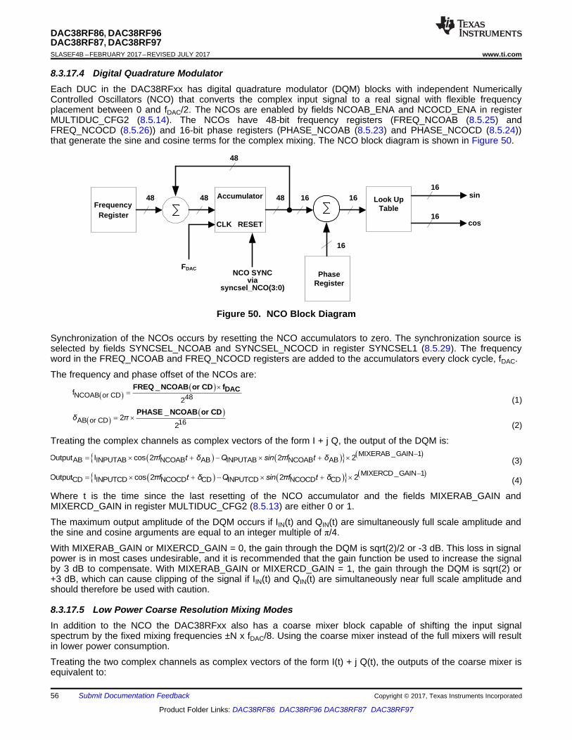
� � � �^ ` � �MIXERCD GAINCD INPUTCD NCOCD CD INPUTCD NCOCD CDOutput I cos �I W �/ 4 VLQ �I W �/
_ 12 2 2 � u � � u � u
� � � �^ ` � �MIXERAB GAINAB INPUTAB NCOAB AB INPUTAB NCOAB ABOutput I cos �I W �/ 4 VLQ �I W �/
_ 12 2 2 � u � � u � u
� �� �
AB or CD/ �16
_2
2 u
PHASE NCOAB or CD
� �� �
NCOAB or CDf48
_
2
u DACFREQ NCOAB or CD f
FrequencyRegister
48 Accumulator48
RESETCLK
FDACNCO SYNC
viasyncsel_NCO(3:0)
48
48
PhaseRegister
16
16
16 Look UpTable
16
16
sin
cos
56
DAC38RF86, DAC38RF96DAC38RF87, DAC38RF97SLASEF4B –FEBRUARY 2017–REVISED JULY 2017 www.ti.com
Product Folder Links: DAC38RF86 DAC38RF96 DAC38RF87 DAC38RF97
Submit Documentation Feedback Copyright © 2017, Texas Instruments Incorporated
8.3.17.4 Digital Quadrature ModulatorEach DUC in the DAC38RFxx has digital quadrature modulator (DQM) blocks with independent NumericallyControlled Oscillators (NCO) that converts the complex input signal to a real signal with flexible frequencyplacement between 0 and fDAC/2. The NCOs are enabled by fields NCOAB_ENA and NCOCD_ENA in registerMULTIDUC_CFG2 (8.5.14). The NCOs have 48-bit frequency registers (FREQ_NCOAB (8.5.25) andFREQ_NCOCD (8.5.26)) and 16-bit phase registers (PHASE_NCOAB (8.5.23) and PHASE_NCOCD (8.5.24))that generate the sine and cosine terms for the complex mixing. The NCO block diagram is shown in Figure 50.
Figure 50. NCO Block Diagram
Synchronization of the NCOs occurs by resetting the NCO accumulators to zero. The synchronization source isselected by fields SYNCSEL_NCOAB and SYNCSEL_NCOCD in register SYNCSEL1 (8.5.29). The frequencyword in the FREQ_NCOAB and FREQ_NCOCD registers are added to the accumulators every clock cycle, fDAC.
The frequency and phase offset of the NCOs are:
(1)
(2)
Treating the complex channels as complex vectors of the form I + j Q, the output of the DQM is:
(3)
(4)
Where t is the time since the last resetting of the NCO accumulator and the fields MIXERAB_GAIN andMIXERCD_GAIN in register MULTIDUC_CFG2 (8.5.13) are either 0 or 1.
The maximum output amplitude of the DQM occurs if IIN(t) and QIN(t) are simultaneously full scale amplitude andthe sine and cosine arguments are equal to an integer multiple of π/4.
With MIXERAB_GAIN or MIXERCD_GAIN = 0, the gain through the DQM is sqrt(2)/2 or -3 dB. This loss in signalpower is in most cases undesirable, and it is recommended that the gain function be used to increase the signalby 3 dB to compensate. With MIXERAB_GAIN or MIXERCD_GAIN = 1, the gain through the DQM is sqrt(2) or+3 dB, which can cause clipping of the signal if IIN(t) and QIN(t) are simultaneously near full scale amplitude andshould therefore be used with caution.
8.3.17.5 Low Power Coarse Resolution Mixing ModesIn addition to the NCO the DAC38RFxx also has a coarse mixer block capable of shifting the input signalspectrum by the fixed mixing frequencies ±N x fDAC/8. Using the coarse mixer instead of the full mixers will resultin lower power consumption.
Treating the two complex channels as complex vectors of the form I(t) + j Q(t), the outputs of the coarse mixer isequivalent to:
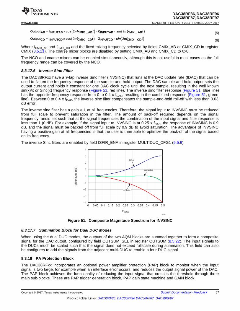
0 0.05 0.1 0.15 0.2 0.25 0.3 0.35 0.4 0.45 0.5–4
–3
–2
–1
0
1
2
3
4
f/fDAC
Ma
gn
itu
de
(d
B)
G056
sin(x)/x
Corrected
FIR4
� � � �_ _2 2 u � uCD INPUTCD CMIX CD INPUTCD CMIX CDOutput I cos �I W 4 VLQ �I W
� � � �_ _2 2 u � uAB INPUTAB CMIX AB INPUTAB CMIX ABOutput I cos �I W 4 VLQ �I W
57
DAC38RF86, DAC38RF96DAC38RF87, DAC38RF97
www.ti.com SLASEF4B –FEBRUARY 2017–REVISED JULY 2017
Product Folder Links: DAC38RF86 DAC38RF96 DAC38RF87 DAC38RF97
Submit Documentation FeedbackCopyright © 2017, Texas Instruments Incorporated
(5)
(6)
Where fCMIX_AB and fCMIX_CD and the fixed mixing frequency selected by fields CMIX_AB or CMIX_CD in registerCMIX (8.5.21). The coarse mixer blocks are disabled by setting CMIX_AB and CMIX_CD to 0x0.
The NCO and coarse mixers can be enabled simultaneously, although this is not useful in most cases as the fullfrequency range can be covered by the NCO.
8.3.17.6 Inverse Sinc FilterThe DAC38RFxx have a 9-tap inverse Sinc filter (INVSINC) that runs at the DAC update rate (fDAC) that can beused to flatten the frequency response of the sample-and-hold output. The DAC sample-and-hold output sets theoutput current and holds it constant for one DAC clock cycle until the next sample, resulting in the well knownsin(x)/x or Sinc(x) frequency response (Figure 51, red line). The inverse sinc filter response (Figure 51, blue line)has the opposite frequency response from 0 to 0.4 x fDAC, resulting in the combined response (Figure 51, greenline). Between 0 to 0.4 x fDAC, the inverse sinc filter compensates the sample-and-hold roll-off with less than 0.03dB error.
The inverse sinc filter has a gain > 1 at all frequencies. Therefore, the signal input to INVSINC must be reducedfrom full scale to prevent saturation in the filter. The amount of back-off required depends on the signalfrequency, andis set such that at the signal frequencies the combination of the input signal and filter response isless than 1 (0 dB). For example, if the signal input to INVSINC is at 0.25 x fDAC, the response of INVSINC is 0.9dB, and the signal must be backed off from full scale by 0.9 dB to avoid saturation. The advantage of INVSINChaving a positive gain at all frequencies is that the user is then able to optimize the back-off of the signal basedon its frequency.
The inverse Sinc filters are enabled by field ISFIR_ENA in register MULTIDUC_CFG1 (9.5.9).
Figure 51. Composite Magnitude Spectrum for INVSINC
8.3.17.7 Summation Block for Dual DUC ModesWhen using the dual DUC modes, the outputs of the two AQM blocks are summed together to form a compositesignal for the DAC output, configured by field OUTSUM_SEL in register OUTSUM (8.5.22). The input signals tothe DUCs much be scaled such that the signal does not exceed fullscale during summation. This field can alsobe configures to add the signals from the adjacent multi-DUC to enable a four DUC signal.
8.3.18 PA Protection BlockThe DAC38RFxx incorporates an optional power amplifier protection (PAP) block to monitor when the inputsignal is two large, for example when an interface error occurs, and reduces the output signal power of the DAC.The PAP block achieves the functionality of reducing the input signal that crosses the threshold through threemain sub-blocks. These are PAP trigger generation block, PAP gain state machine and GAIN block.
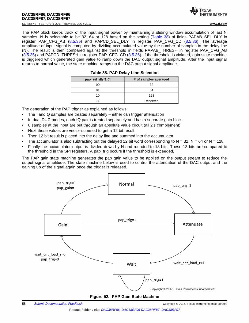
Normal
Attenuate
Wait
Gain
pap_trig=1
pap_trig=1
wait_cnt_load_r=1
wait_cnt_load_r=0
pap_trig=0
pap_trig=0
pap_gain=1
pap_trig=1
Copyright © 2017, Texas Instruments Incorporated
58
DAC38RF86, DAC38RF96DAC38RF87, DAC38RF97SLASEF4B –FEBRUARY 2017–REVISED JULY 2017 www.ti.com
Product Folder Links: DAC38RF86 DAC38RF96 DAC38RF87 DAC38RF97
Submit Documentation Feedback Copyright © 2017, Texas Instruments Incorporated
The PAP block keeps track of the input signal power by maintaining a sliding window accumulation of last Nsamples. N is selectable to be 32, 64 or 128 based on the setting (Table 38) of fields PAPAB_SEL_DLY inregister PAP_CFG_AB (8.5.35) and PAPCD_SEL_DLY in register PAP_CFG_CD (8.5.36). The averageamplitude of input signal is computed by dividing accumulated value by the number of samples in the delay-line(N). The result is then compared against the threshold in fields PAPAB_THRESH in register PAP_CFG_AB(8.5.35) and PAPCD_THRESH in register PAP_CFG_CD (8.5.36). If the threshold is violated, gain state machineis triggered which generated gain value to ramp down the DAC output signal amplitude. After the input signalreturns to normal value, the state machine ramps up the DAC output signal amplitude.
Table 38. PAP Delay Line Selectionpap_sel_dly[1:0] # of samples averaged
00 3201 6410 12811 Reserved
The generation of the PAP trigger as explained as follows:• The I and Q samples are treated separately – either can trigger attenuation• In dual DUC modes, each IQ pair is treated separately and has a separate gain block• 8 samples at the input are put through an absolute value circuit (all 2’s complement)• Next these values are vector summed to get a 12 bit result• Then 12 bit result is placed into the delay line and summed into the accumulator• The accumulator is also subtracting out the delayed 12 bit word corresponding to N = 32, N = 64 or N = 128• Finally the accumulator output is divided down by N and rounded to 13 bits. These 13 bits are compared to
the threshold in the SPI registers. A pap_trig occurs if the threshold is exceeded.
The PAP gain state machine generates the pap gain value to be applied on the output stream to reduce theoutput signal amplitude. The state machine below is used to control the attenuation of the DAC output and thegaining up of the signal again once the trigger is released.
Figure 52. PAP Gain State Machine
output AB CD AB CDOUTSUM SAME SAME ADJ ADJ � � �
59
DAC38RF86, DAC38RF96DAC38RF87, DAC38RF97
www.ti.com SLASEF4B –FEBRUARY 2017–REVISED JULY 2017
Product Folder Links: DAC38RF86 DAC38RF96 DAC38RF87 DAC38RF97
Submit Documentation FeedbackCopyright © 2017, Texas Instruments Incorporated
The normal operating condition for the PAP block is the NORMAL state in Figure 52. However, when the PAPblock detects an error condition it sets the pap_trig signal to ‘1’ causing a state transition from NORMALoperation to the ATTENUATE state.
In the ATTENUTATE state the data path gain is scaled from 1.0 down to 0.0 by a programmable step amount setby fields PAPAB_GAIN_STEP in register PAP_GAIN_AB (8.5.31) and PAPCD_GAIN_STEP in registerPAP_GAIN_CD (8.5.33). This value is always positive with the decimal place located between the MSB andMSB-1. Unity is equal to “1000000000”. Each clock cycle (16 samples) the PAP_GAIN is stepped down byPAPAB_GAIN_STEP and PAPCD_GAIN_STEP until the gain is 0.
After PAP_GAIN is 0, the state machine moves on to the WAIT state. Here a programmable counter counts clockcycles to allow the condition for the pap_trig to be fixed. Fields PAPAB_WAIT in register PAP_WAIT_AB (8.5.32)and PAPCD_WAIT in register PAP_WAIT_CD (8.5.34) are used to select the number of clock cycles (samples =16 x PAPAB_WAIT or 16 x PAPCD_WAIT) to wait before moving to the next state. Once the WAIT counterequals zero and pap_trig=’0’, the state machine moves on to the GAIN state. If the WAIT equals 0 but pap_trigstill equals ‘1’ then the state machine stays in the WAIT state until pap_trig =’0’.
8.3.19 Gain BlockThe GAIN block also has additional output gain control through fields GAINAB in register GAINAB (8.5.39) andGAINCD in register GAINCD (8.5.40). Similar to PAP_GAIN value, the output gain is always positive with unitywhen GAINAB or GAINCD = ”010000000000”.
To reduce the power, the gain block clock has been gated whenever the pap is disabled and GAINAB orGAINCD is set to unity.
8.3.20 Output SummationThe OUTSUM block allows addition of samples from each DUC in the multi-DUC. It is also possible to add theoutput samples from the adjacent multi-DUC. Field OUTSUM_SEL in register OUTSUM (8.5.22) controls thesummation for each multi-DUC. The functionality of the block can be represented by the following equation:
(7)
In order to avoid overflow, rounding operation is performed after the addition to reduce the word size back to 16-bits. Exact number of bits rounded depends on the number of channels added. Table 39 shows the description ofround after the summation.
Table 39. OUTSUM Scaling and Rounding# OF CHANNELS ADDED # OF BITS ROUNDED
0 0, Use bits[15:0] from the result1 Use bits[16:1] from the result and bit[0] used for rounding2 Use bits[17:2] from the result and bits[1:0] used for rounding3 Use bits[18:3] from the result and bit[2:0] used for rounding4 Use bits[19:4] from the result and bit[3:0] used for rounding
8.3.21 Output DelayThe signal following output summation can be programmably delayed by 0-15 DACCLK cycles through fieldOUTPUT_DELAY in register OUTSUM (8.5.20). The block takes 16 sample words (vec16) from both the A and Bpaths and shifts the them to 32 sample long delay line.
8.3.22 Polarity InversionThe signal following the output delay can be inverted by a 2’s complement conversion allowing the + and - DACoutputs to be swapped by asserting field DAC_COMPLEMENT in register MULTIDUC_CFG1 (8.5.13).
8.3.23 Temperature SensorThe DAC38RFxx incorporates a temperature sensor block which monitors the die temperature by measuring thevoltage across 2 transistors. The voltage is converted to an 8-bit digital word using a successive approximation(SAR) analog to digital conversion process. The result is scaled, limited and formatted as a twos complementvalue representing the temperature in degrees Celsius.

60
DAC38RF86, DAC38RF96DAC38RF87, DAC38RF97SLASEF4B –FEBRUARY 2017–REVISED JULY 2017 www.ti.com
Product Folder Links: DAC38RF86 DAC38RF96 DAC38RF87 DAC38RF97
Submit Documentation Feedback Copyright © 2017, Texas Instruments Incorporated
The sampling is controlled by the serial interface signals SDEN and SCLK. If the temperature sensor is enabledby writing a 0 to field TSENSE_SLEEP in register SLEEP_CONFIG (8.5.70), a conversion takes place each timethe serial port is written or read. The data is only read and sent out by the digital block when the temperaturesensor is read in field TEMPDATA in register TEMP_PLLVOLT (8.5.7). The conversion uses the first eight clocksof the serial clock as the capture and conversion clock, the data is valid on the falling eighth SCLK. The data isthen clocked out of the chip on the rising edge of the ninth SCLK. No other clocks to the chip are necessary forthe temperature sensor operation. As a result the temperature sensor is enabled even when the device is insleep mode.
In order for the process described above to operate properly, the serial port read from register TEMP_PLLVOLTmust be done with an SCLK period of at least 1 μs. If this is not satisfied the temperature sensor accuracy isgreatly reduced.
8.3.24 Alarm MonitoringThe DAC38RFxx includes a flexible set of alarm monitoring that can be used to alert of a possible malfunctionscenario. All the alarm events can be accessed either through the SIP registers and/or through the ALARMoutput. Once an alarm is set, the corresponding alarm bit must be reset through the serial interface to allowfurther testing. The set of alarms includes the following conditions:• JESD alarms
– Fields ALM_LANEx_ERR in registers JESD_ALM_Lx (x = 0-7, 8.5.59 to 8.5.66):– multiframe alignment_error. Occurs when multiframe alignment fails– frame alignment error. Occurs when multiframe alignment fails– link configuration error. Occurs when there is wrong link configuration– elastic buffer overflow. Occurs when bad RBD value is used– elastic buffer match error. Occurs when the first non-/K/ doesn’t match the programmed data– code synchronization error– 8b/10b not-in-table decode error– 8b/10b disparity error
– Field ALM_FROM_SHORTTEST in register ALM_SYSREF_PAP (8.5.67): Occurs when the short patterntest fails.
• SerDes alarms– Field ALM_SD_LOTDET in register ALM_SD_DET 8.5.5): Occurs when there are loss of signal detect
from SerDes lanes.– Fields ALM_FIFOx_FLAGS in registers JESD_ALM_Lx (x = 0-7, 8.5.59 to 8.5.66):
– FIFO write error. Occurs if write request and FIFO is full.– FIFO write full: Occurs if FIFO is full.– FIFO read error. Occurs if read request and FIFO is empty.– FIFO read empty: Occurs if FIFO is empty.
– Field ALM_SD0_PLL in register ALM_SYSREF_DET (8.5.6): Occurs if the PLL in the SerDes block 0goes out of lock.
– Field ALM_SD1_PLL in register ALM_SYSREF_DET (8.5.6): Occurs if the PLL in the SerDes block 1goes out of lock.
• SYSREF alarm– Field ALM_SYSREF_ERR in register ALM_SYSREF_PAP (8.5.67): Occurs when the SYSREF is received
at an unexpected time. If too many of these occur it will cause the JESD to go into synchronization modeagain.
• DAC PLL alarm– Field PLL_LOCK in register ALM_SYSREF_DET (8.5.6). This register field is asserted when the PLL is
unlocked. When used as an alarm output, a high signal indicates that the PLL is unlocked if theALM_OUT_POL bit in register RESET_CONFIG is set to 1.
• PAP alarm– Field ALM_PAP in register ALM_SYSREF_PAP (8.5.67): Occurs when the average power is above the
threshold. While any alarm_pap is asserted the attenuation for the appropriate data path is applied.
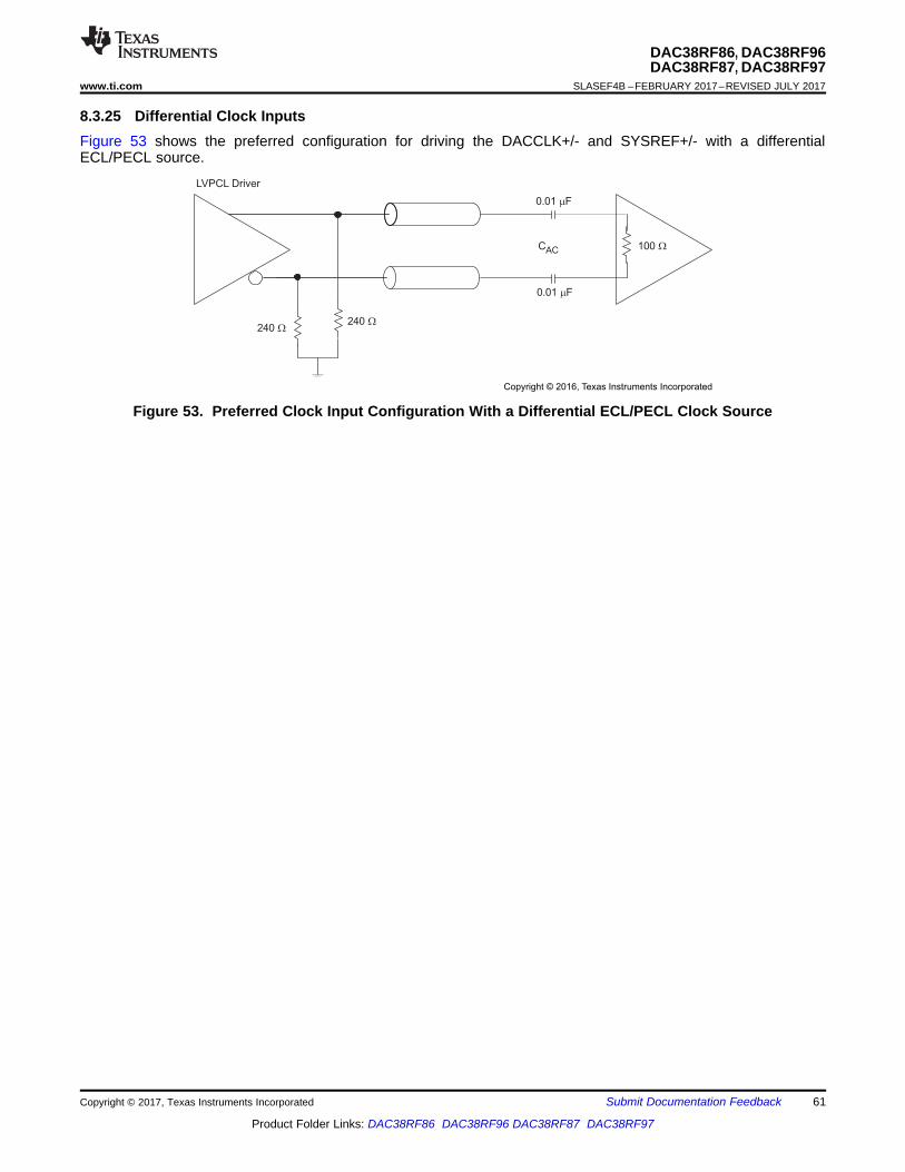
LVPCL Driver
240 W240 W
100 W
0.01 Fm
0.01 Fm
CAC
Copyright © 2016, Texas Instruments Incorporated
61
DAC38RF86, DAC38RF96DAC38RF87, DAC38RF97
www.ti.com SLASEF4B –FEBRUARY 2017–REVISED JULY 2017
Product Folder Links: DAC38RF86 DAC38RF96 DAC38RF87 DAC38RF97
Submit Documentation FeedbackCopyright © 2017, Texas Instruments Incorporated
8.3.25 Differential Clock InputsFigure 53 shows the preferred configuration for driving the DACCLK+/- and SYSREF+/- with a differentialECL/PECL source.
Figure 53. Preferred Clock Input Configuration With a Differential ECL/PECL Clock Source

� �coarsetrimI = 2mA × DACFS -11
BGRBIAS
BIAS
V VI mA
R k0.9
128 128 323.6
u u
FS RBIAS coarsetrimIOUT I I �
SDIO
SCLK
TCLK
SLEEP
TXENABLE
TESTMODE
internal
digital in
VDDIO18
GND
SDENB
RESETB
TMS
TDI
TRSTB
internal
digital in
VDDIO18
GND
400 400
10 k
10 k
Copyright © 2016, Texas Instruments Incorporated
62
DAC38RF86, DAC38RF96DAC38RF87, DAC38RF97SLASEF4B –FEBRUARY 2017–REVISED JULY 2017 www.ti.com
Product Folder Links: DAC38RF86 DAC38RF96 DAC38RF87 DAC38RF97
Submit Documentation Feedback Copyright © 2017, Texas Instruments Incorporated
(1) The bias current per each complementary output is half the total bias current
8.3.26 CMOS Digital InputsFigure 54 shows a schematic of the equivalent CMOS digital inputs of the DAC38RFxx. SDIO, SCLK, TCLK,SLEEP, TESTMODE and TXENABLE have internal pull-down resistors while SDEN, RESET, TMS, TDI andTRST have internal pull-up resistors. See the Specifications table for logic thresholds. The pull-up and pull-downcircuitry is approximately equivalent to 10 kΩ.
Figure 54. CMOS Digital Equivalent Input
8.3.27 DAC Fullscale Output CurrentThe DAC38RFxx uses a bandgap reference and control amplifier for biasing the full-scale output current. TheDAC full scale output current is set by a combination of the fixed current through the external resistor RBIAS(connected to pin BIASJ) and current from course trim current sources:
(8)
The bias current IBIAS through resistor RBIAS is defined by the on-chip bandgap reference voltage VBG (nominally0.9 V) and control amplifier. For normal operation, it is recommended that RBIAS is set to 3.6 kΩ for a fixedcurrent through RBIAS of 250 µA. This current is scaled 128x internally, giving:
(9)
The course trim current sources are configured through SPI register field DACFS in register DACFS (8.5.72),asfollows:
(10)
From the discussion above, the DAC full scale output current can be configured from 40 mA (DACFS[3:0] =1111) down to 10 mA (DACFS[3:0] = 0000). In addition to the full scale signal current set by SPI register DACFS(8.5.72), an extra DC bias current is required to set the operating point of the output current sources(Table 40).
Table 40. DAC output currentDACFS ( 8.5.72) Signal current (mA) Total bias current (mA) (1)
0 10 11 12 12 14 23 16 24 18 35 20 36 22 47 24 58 26 59 28 6
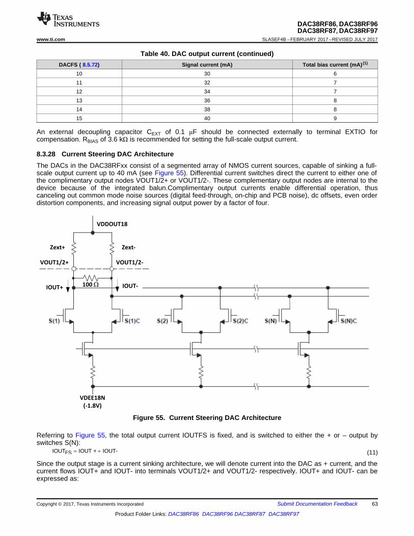
FSIOUT IOUT + IOUT- �
VDEE18N
(-1.8V)
VOUT1/2+ VOUT1/2-
100 :
Zext+ Zext-
VDDOUT18
IOUT+ IOUT-
63
DAC38RF86, DAC38RF96DAC38RF87, DAC38RF97
www.ti.com SLASEF4B –FEBRUARY 2017–REVISED JULY 2017
Product Folder Links: DAC38RF86 DAC38RF96 DAC38RF87 DAC38RF97
Submit Documentation FeedbackCopyright © 2017, Texas Instruments Incorporated
Table 40. DAC output current (continued)DACFS ( 8.5.72) Signal current (mA) Total bias current (mA) (1)
10 30 611 32 712 34 713 36 814 38 815 40 9
An external decoupling capacitor CEXT of 0.1 μF should be connected externally to terminal EXTIO forcompensation. RBIAS of 3.6 kΩ is recommended for setting the full-scale output current.
8.3.28 Current Steering DAC ArchitectureThe DACs in the DAC38RFxx consist of a segmented array of NMOS current sources, capable of sinking a full-scale output current up to 40 mA (see Figure 55). Differential current switches direct the current to either one ofthe complimentary output nodes VOUT1/2+ or VOUT1/2-. These complementary output nodes are internal to thedevice because of the integrated balun.Complimentary output currents enable differential operation, thuscanceling out common mode noise sources (digital feed-through, on-chip and PCB noise), dc offsets, even orderdistortion components, and increasing signal output power by a factor of four.
Figure 55. Current Steering DAC Architecture
Referring to Figure 55, the total output current IOUTFS is fixed, and is switched to either the + or – output byswitches S(N):
(11)
Since the output stage is a current sinking architecture, we will denote current into the DAC as + current, and thecurrent flows IOUT+ and IOUT- into terminals VOUT1/2+ and VOUT1/2- respectively. IOUT+ and IOUT- can beexpressed as:
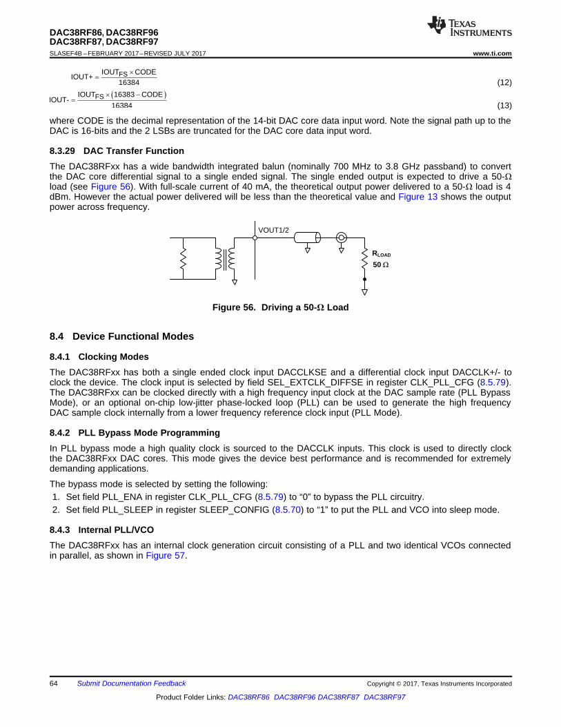
50 :
RLOAD
VOUT1/2
� �FSIOUT CODEIOUT-
16383
16384
u �
FSIOUT CODEIOUT+
16384u
64
DAC38RF86, DAC38RF96DAC38RF87, DAC38RF97SLASEF4B –FEBRUARY 2017–REVISED JULY 2017 www.ti.com
Product Folder Links: DAC38RF86 DAC38RF96 DAC38RF87 DAC38RF97
Submit Documentation Feedback Copyright © 2017, Texas Instruments Incorporated
(12)
(13)
where CODE is the decimal representation of the 14-bit DAC core data input word. Note the signal path up to theDAC is 16-bits and the 2 LSBs are truncated for the DAC core data input word.
8.3.29 DAC Transfer FunctionThe DAC38RFxx has a wide bandwidth integrated balun (nominally 700 MHz to 3.8 GHz passband) to convertthe DAC core differential signal to a single ended signal. The single ended output is expected to drive a 50-Ωload (see Figure 56). With full-scale current of 40 mA, the theoretical output power delivered to a 50-Ω load is 4dBm. However the actual power delivered will be less than the theoretical value and Figure 13 shows the outputpower across frequency.
Figure 56. Driving a 50-Ω Load
8.4 Device Functional Modes
8.4.1 Clocking ModesThe DAC38RFxx has both a single ended clock input DACCLKSE and a differential clock input DACCLK+/- toclock the device. The clock input is selected by field SEL_EXTCLK_DIFFSE in register CLK_PLL_CFG (8.5.79).The DAC38RFxx can be clocked directly with a high frequency input clock at the DAC sample rate (PLL BypassMode), or an optional on-chip low-jitter phase-locked loop (PLL) can be used to generate the high frequencyDAC sample clock internally from a lower frequency reference clock input (PLL Mode).
8.4.2 PLL Bypass Mode ProgrammingIn PLL bypass mode a high quality clock is sourced to the DACCLK inputs. This clock is used to directly clockthe DAC38RFxx DAC cores. This mode gives the device best performance and is recommended for extremelydemanding applications.
The bypass mode is selected by setting the following:1. Set field PLL_ENA in register CLK_PLL_CFG (8.5.79) to “0” to bypass the PLL circuitry.2. Set field PLL_SLEEP in register SLEEP_CONFIG (8.5.70) to “1” to put the PLL and VCO into sleep mode.
8.4.3 Internal PLL/VCOThe DAC38RFxx has an internal clock generation circuit consisting of a PLL and two identical VCOs connectedin parallel, as shown in Figure 57.
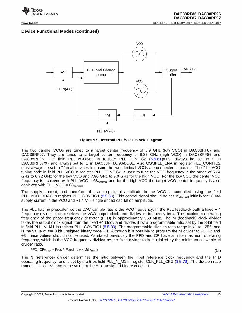
� �Fmax minPFD CP Fvco Fixed div x Mdiv_ / _
÷NPFD and Charge
pumpOutput buffer
÷4÷M
PLL_M(7-0)
PLL_N(4-0)
VCO
VCO
DAC CLK
65
DAC38RF86, DAC38RF96DAC38RF87, DAC38RF97
www.ti.com SLASEF4B –FEBRUARY 2017–REVISED JULY 2017
Product Folder Links: DAC38RF86 DAC38RF96 DAC38RF87 DAC38RF97
Submit Documentation FeedbackCopyright © 2017, Texas Instruments Incorporated
Device Functional Modes (continued)
Figure 57. Internal PLL/VCO Block Diagram
The two parallel VCOs are tuned to a target center frequency of 5.9 GHz (low VCO) in DAC38RF87 andDAC38RF97. They are tuned to a target center frequency of 8.85 GHz (high VCO) in DAC38RF86 andDAC38RF96. The field PLL_VCOSEL in register PLL_CONFIG2 (8.5.81)must always be set to 0 inDAC38RF87/97 and always set to '1' in DAC38RF86/96/88/81. Also GSMPLL_ENA in register PLL_CONFIG2must always be set to '1' in all devices to ensure the two identical VCOs are connected in parallel. The 7 bit VCOtuning code in field PLL_VCO in register PLL_CONFIG2 is used to tune the VCO frequency in the range of 5.24GHz to 6.72 GHz for the low VCO and 7.96 GHz to 9.0 GHz for the high VCO. For the low VCO the center VCOfrequency is achieved with PLL_VCO = 63decimal and for the high VCO the target VCO center frequency is alsoachieved with PLL_VCO = 63decimal.
The supply current, and therefore; the analog signal amplitude in the VCO is controlled using the fieldPLL_VCO_RDAC in register PLL_CONFIG1 (8.5.80). This control signal should be set 15decimal initially for 18 mAsupply current in the VCO and ~1.4 VPP single ended oscillation amplitude.
The PLL has no prescaler, so the DAC sample rate is the VCO frequency. In the PLL feedback path a fixed ÷ 4frequency divider block receives the VCO output clock and divides its frequency by 4. The maximum operatingfrequency of the phase-frequency detector (PFD) is approximately 550 MHz. The M (feedback) clock dividertakes the output clock signal from the fixed ÷4 block and divides it by a programmable ratio set by the 8-bit fieldin field PLL_M_M1 in register PLL_CONFIG1 (8.5.80). The programmable division ratio range is ÷1 to ÷256, andis the value of the 8 bit unsigned binary code + 1. Although it is possible to program the M divider to ÷1, ÷2 and÷3, these values should not be used. As stated previously the PFD and CP have a finite maximum operatingfrequency, which is the VCO frequency divided by the fixed divider ratio multiplied by the minimum allowable Mdivider ratio.
(14)
The N (reference) divider determines the ratio between the input reference clock frequency and the PFDoperating frequency, and is set by the 5-bit field PLL_N_M1 in register CLK_PLL_CFG (8.5.79). The division ratiorange is ÷1 to ÷32, and is the value of the 5-bit unsigned binary code + 1.
66
DAC38RF86, DAC38RF96DAC38RF87, DAC38RF97SLASEF4B –FEBRUARY 2017–REVISED JULY 2017 www.ti.com
Product Folder Links: DAC38RF86 DAC38RF96 DAC38RF87 DAC38RF97
Submit Documentation Feedback Copyright © 2017, Texas Instruments Incorporated
Device Functional Modes (continued)The charge pump output current amplitude is set using the 4-bit field PLL_CP_ADJ in in register PLL_CONFIG2(8.5.81). The current amplitude is simply the digital code multiplied by the unit current amplitude of 100 µA. In anominal condition, with the LF VCO running at 5.898 GHz, and with the M divider set to ÷4, the PFD will run at368.625 MHz, and the change pump current should set to 6decimal, which gives 600 µA charge pump outputcurrent for a good phase margin of 69 degrees. If a higher M ratio (for lower PFD frequencies) are required thecharge pump output current must be increased to maintain good loop stability and prevent excessive peaking inthe phase noise response. The charge pump output current setting PLL_CP_ADJ should be adjusted in relationto the feedback (M) divider ratio PLL_M_M1 according to the following table to maintain a constant phase marginof 69 degrees.
Table 41. M vs Kp for Maintaining Good StabilityM CP_ADJ4 66 98 1210 15
Similarly for the HF VCO running at 8.847 GHz, and with the M divider set to ÷4, the PFD will run at 552.9375MHz as shown above. Here the change pump current should set to 6decimal, which gives 600 µA charge pumpoutput current for a good phase margin of 69 degrees.
8.4.4 CLKOUTThe DAC38RFxx has a programmable output clock on CLKTX+/- balls that is a divided version of the internalDAC sample clock, either with or without PLL. Two frequency dividers, either DACCLK/3 or DACCLK/4, areavailable by programming field CLK_TX_DIV4 in register CLK_OUT (8.5.71). The output swing voltage isprogrammable from approximately 125 to 1460 mVPP-DIFF through field CLK_TX_SWING in register CLK_OUT(8.5.71).
Field CLK_TX_IDLE in register CLK_OUT (8.5.71) enables an idle state, in which the pins are driven to theproper common-mode levels in order to charge the external AC coupling caps but the clock output is disabled.The output clock circuit can be put to sleep by field CLK_TX_SLEEP in register SLEEP_CONFIG (8.5.70).
8.4.5 Serial Peripheral Interface (SPI)The serial port of the DAC38RFxx is a flexible serial interface which communicates with industry standardmicroprocessors and microcontrollers. The interface provides read/write access to all registers used to define theoperating modes of DAC38RFxx. It is compatible with most synchronous transfer formats and can be configuredas a 3 or 4 terminal interface by SIF4_ENA in register IO_CONFIG (8.5.2). In both configurations, SCLK is theserial interface input clock and SDEN is serial interface enable. For 3 terminal configuration, SDIO is abidirectional terminal for both data in and data out. For 4 terminal configuration, SDIO is bidirectional and SDO isdata out only. Data is input into the device with the rising edge of SCLK. Data is output from the device on thefalling edge of SCLK.
The SPI registers are reset by writing a 1 to SPI_RESET in register RESET_CONFIG (8.5.1).
Each read/write operation is framed by signal SDEN (Serial Data Enable Bar) asserted low. The first frame byteis the instruction cycle which identifies the following data transfer cycle as read or write as well as the 7-bitaddress to be accessed. Figure 58 indicates the function of each bit in the instruction cycle and is followed by adetailed description of each bit. The data transfer cycle consists of two bytes.
Figure 58. Instruction Byte of the Serial Interface
Bit 7 (MSB) 6 5 4 3 2 1 0Description R/W A6 A5 A4 A3 A2 A1 A0
R/W - Identifies the following data transfer cycle as a read or write operation. A high indicates a read operation from DAC38RFxx and a lowindicates a write operation to DAC38RFxxA6:A0 - Identifies the address of the register to be accessed during the read or write operation.

rwb A6 A5 A4 A3 A2 A1 A0 D15 D14 D13 D12 D11 D10 D9 D8 D7 D6 D5 D4 D3 D2 D1 D0
Instruction Cycle Data Transfer Cycle
td(Data)
SDEN\
SCLK
SDIO
SDEN\
SCLK
SDIOSDO
D15 D14 D13 D12 D11 D10 D9 D8 D7 D6 D5 D4 D3 D2 D1 D0SDO
Data n Data n-1
rwb A6 A5 A4 A3 A2 A1 A0 D15 D14 D13 D12 D11 D10 D9 D8 D7 D6 D5 D4 D3 D2 D1 D0
Instruction Cycle Data Transfer Cycle
tS(SDEN\)
tS(SDIO) tH(SDIO)
tSCLK
SDEN\
SCLK
SDIO
SDEN\
SCLK
SDIO
67
DAC38RF86, DAC38RF96DAC38RF87, DAC38RF97
www.ti.com SLASEF4B –FEBRUARY 2017–REVISED JULY 2017
Product Folder Links: DAC38RF86 DAC38RF96 DAC38RF87 DAC38RF97
Submit Documentation FeedbackCopyright © 2017, Texas Instruments Incorporated
Figure 59 shows the serial interface timing diagram for a DAC38RFxx write operation. SCLK is the serialinterface clock input to DAC38RFxx. Serial data enable SDEN is an active low input to DAC38RFxx. SDIO isserial data input. Input data to DAC38RFxx is clocked on the rising edges of SCLK.
Figure 59. Serial Interface Write Timing Diagram
Figure 60 shows the serial interface timing diagram for a DAC38RFxx read operation. SCLK is the serialinterface clock input to DAC38RFxx. Serial data enable SDEN\ is an active low input to DAC38RFxx. SDIO isserial data input during the instruction cycle. In 3 pin configuration, SDIO is data out from the DAC38RFxx duringthe data transfer cycle, while SDO is in a high-impedance state. In 4 pin configuration, both SDIO and SDO aredata out from the DAC38RFxx during the data transfer cycle. At the end of the data transfer, SDIO and SDO willoutput low on the final falling edge of SCLK until the rising edge of SDEN when they will 3-state.
Figure 60. Serial Interface Read Timing Diagram
n the SIF interface there are four types of registers:
8.4.5.1 NORMAL (RW)The NORMAL register type allows data to be written and read from. All 16-bits of the data are registered at thesame time. There is no synchronizing with an internal clock thus all register writes are asynchronous with respectto internal clocks. There are three subtypes of NORMAL:1. AUTOSYNC: A NORMAL register that causes a sync to be generated after the write is finished. These are
used when it is desirable to synchronize the block after writing the register or for a single field that spansacross multiple registers. For instance, the NCO requires three 16-bit register writes to set the frequency.Upon writing the last of these registers an autosync is generated to deliver the entire field to the NCO blockat once, rather than in pieces after each individual register write. For a field that spans multiple registers, allnon-AUTOSYNC registers for the field must be written first before the actual AUTOSYNC register.
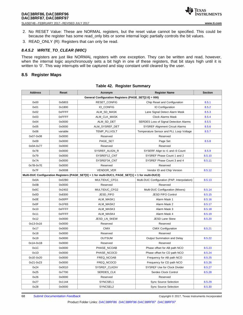
68
DAC38RF86, DAC38RF96DAC38RF87, DAC38RF97SLASEF4B –FEBRUARY 2017–REVISED JULY 2017 www.ti.com
Product Folder Links: DAC38RF86 DAC38RF96 DAC38RF87 DAC38RF97
Submit Documentation Feedback Copyright © 2017, Texas Instruments Incorporated
2. No RESET Value: These are NORMAL registers, but the reset value cannot be specified. This could bebecause the register has some read_only bits or some internal logic partially controls the bit values.
3. READ_ONLY (R): Registers that can only be read.
8.4.5.2 WRITE_TO_CLEAR (W0C)These registers are just like NORMAL registers with one exception. They can be written and read, however,when the internal logic asynchronously sets a bit high in one of these registers, that bit stays high until it iswritten to ‘0’. This way interrupts will be captured and stay constant until cleared by the user.
8.5 Register Maps
Table 42. Register SummaryAddress Reset Acronym Register Name Section
General Configuration Registers (PAGE_SET[2:0] = 000)
0x00 0x5803 RESET_CONFIG Chip Reset and Configuration 8.5.1
0x01 0x1800 IO_CONFIG IO Configuration 8.5.2
0x02 0xFFFF ALM_SD_MASK Lane Signal Detect Alarm Mask 8.5.3
0x03 0xFFFF ALM_CLK_MASK Clock Alarms Mask 8.5.4
0x04 0x0000 ALM_SD_DET SERDES Loss of Signal Detection Alarms 8.5.5
0x05 0x0000 ALM_SYSREF_DET SYSREF Alignment Circuit Alarms 8.5.6
0x06 variable TEMP_PLLVOLT Temperature Sensor and PLL Loop Voltage 8.5.7
0x07-0x08 0x0000 Reserved Reserved
0x09 0x0000 PAGE_SET Page Set 8.5.8
0x0A-0x77 0x0000 Reserved Reserved
0x78 0x0000 SYSREF_ALIGN_R SYSERF Align to r1 and r3 Count 8.5.9
0x79 0x0000 SYSREF12_CNT SYSREF Phase Count 1 and 2 8.5.10
0x7A 0x0000 SYSREF34_CNT SYSREF Phase Count 3 and 4 8.5.11
0x7B-0x7E 0x0000 Reserved Reserved
0x7F 0x0008 VENDOR_VER Vendor ID and Chip Version 8.5.12
Multi-DUC Configuration Registers (PAGE_SET[0] = 1 for multi-DUC1, PAGE_SET[1] = 1 for multi-DUC2)
0x0A 0x02B0 MULTIDUC_CFG1 Multi-DUC Configuration (PAP, Interpolation) 8.5.13
0x0B 0x0000 Reserved Reserved
0x0C 0x2402 MULTIDUC_CFG2 Multi-DUC Configuration (Mixers) 8.5.14
0x0D 0x8300 JESD_FIFO JESD FIFO Control 8.5.15
0x0E 0x00FF ALM_MASK1 Alarm Mask 1 8.5.16
0x0F 0x1F83 ALM_MASK2 Alarm Mask 2 8.5.17
0x10 0xFFFF ALM_MASK3 Alarm Mask 3 8.5.18
0x11 0xFFFF ALM_MASK4 Alarm Mask 4 8.5.19
0x12 0x0000 JESD_LN_SKEW JESD Lane Skew 8.5.20
0x13-0x16 0x0000 Reserved Reserved
0x17 0x0000 CMIX CMIX Configuration 8.5.21
0x18 0x0000 Reserved Reserved
0x19 0x0000 OUTSUM Output Summation and Delay 8.5.22
0x1A-0x1B 0x0000 Reserved Reserved
0x1C 0x0000 PHASE_NCOAB Phase offset for AB path NCO 8.5.23
0x1D 0x0000 PHASE_NCOCD Phase offset for CD path NCO 8.5.24
0x1E-0x20 0x0000 FREQ_NCOAB Frequency for AB path NCO 8.5.25
0x21-0x23 0x0000 FREQ_NCOCD Frequency for CD path NCO 8.5.26
0x24 0x0010 SYSREF_CLKDIV SYSREF Use for Clock Divider 8.5.27
0x25 0x7700 SERDES_CLK Serdes Clock Control 8.5.28
0x26 0x0000 Reserved Reserved
0x27 0x1144 SYNCSEL1 Sync Source Selection 8.5.29
0x28 0x0000 SYNCSEL2 Sync Source Selection 8.5.30

69
DAC38RF86, DAC38RF96DAC38RF87, DAC38RF97
www.ti.com SLASEF4B –FEBRUARY 2017–REVISED JULY 2017
Product Folder Links: DAC38RF86 DAC38RF96 DAC38RF87 DAC38RF97
Submit Documentation FeedbackCopyright © 2017, Texas Instruments Incorporated
Register Maps (continued)Table 42. Register Summary (continued)
Address Reset Acronym Register Name Section
0x29 0x0000 PAP_GAIN_AB PAP path AB Gain Attenuation Step 8.5.31
0x2A 0x0000 PAP_WAIT_AB PAP path AB Wait Time at Gain = 0 8.5.32
0x2B 0x0000 PAP_GAIN_CD PAP path CD Gain Attenuation Step 8.5.33
0x2C 0x0000 PAP_WAIT_CD PAP path CD Wait Time at Gain = 0 8.5.34
0x2D 0x1FFF PAP_CFG_AB PAP path AB Configuration 8.5.35
0x2E 0x1FFF PAP_CFG_CD PAP path CD Configuration 8.5.36
0x2F 0x0000 SPIDAC_TEST1 Configuration for DAC SPI Constant 8.5.37
0x30 0x0000 SPIDAC_TEST2 DAC SPI Constant 8.5.38
0x31 0x0000 Reserved Reserved
0x32 0x0800 GAINAB Gain for path AB 8.5.39
0x33 0x0800 GAINCD Gain for path CD 8.5.40
0x34-0x40 0x0000 Reserved Reserved
0x41 0x0000 JESD_ERR_CNT JESD Error Counter 8.5.41
0x42-0x45 0x0000 Reserved Reserved
0x46 0x0044 JESD_ID1 JESD ID 1 8.5.42
0x47 0x190A JESD_ID2 JESD ID 2 8.5.43
0x48 0x31C3 JESD_ID3 JESD ID 3 and Subclass 8.5.44
0x49 0x0000 Reserved Reserved
0x4A 0x0003 JESD_LN_EN JESD Lane Enable 8.5.45
0x4B 0x1300 JESD_RBD_F JESD RBD Buffer and Frame Octets 8.5.46
0x4C 0x1303 JESD_K_L JESD K and L Parameters 8.5.47
0x4D 0x0100 JESD_M_S JESD M and S Parameters 8.5.48
0x4E 0x0F4F JESD_N_HD_SCR JESD N, HD and SCR Parameters 8.5.49
0x4F 0x1CC1 JESD_MATCH JESD Character Match and Other 8.5.50
0x50 0x0000 JESD_LINK_CFG JESD Link Configuration Data 8.5.51
0x51 0x00FF JESD_SYNC_REQ JESD Sync Request 8.5.52
0x52 0x00FF JESD_ERR_OUT JESD Error Output 8.5.53
0x53 0x0100 JESD_ILA_CFG1 JESD Configuration Value used for ILACheck 8.5.54
0x54 0x8E60 JESD_ILA_CFG2 JESD Configuration Value used for ILACheck 8.5.55
0x55-0x5B 0x0000 Reserved Reserved
0x5C 0x0001 JESD_SYSR_MODE JESD SYSREF Mode 8.5.56
0x5D-0x5E 0x0000 Reserved Reserved
0x5F 0x0123 JESD_CROSSBAR1 JESD Crossbar Configuration 1 8.5.57
0x60 0x4567 JESD_CROSSBAR2 JESD Crossbar Configuration 2 8.5.58
0x61-0x63 0x0000 Reserved Reserved
0x64 0x0000 JESD_ALM_L0 JESD Alarms for Lane 0 8.5.59
0x65 0x0000 JESD_ ALM_L1 JESD Alarms for Lane 1 8.5.60
0x66 0x0000 JESD_ ALM_L2 JESD Alarms for Lane 2 8.5.61
0x67 0x0000 JESD_ALM_L3 JESD Alarms for Lane 3 8.5.62
0x68 0x0000 JESD_ALM_L4 JESD Alarms for Lane 4 8.5.63
0x69 0x0000 JESD_ALM_L5 JESD Alarms for Lane 5 8.5.64
0x6A 0x0000 JESD_ALM_L6 JESD Alarms for Lane 6 8.5.65
0x6B 0x0000 JESD_ALM_L7 JESD Alarms for Lane 7 8.5.66
0x6C 0x0000 ALM_SYSREF_PAP SYSREF and PAP Alarms 8.5.67
0x6D 0x0000 ALM_CLKDIV1 Clock Divider Alarms 1 8.5.68
0x6E-0x77 0x0000 Reserved Reserved
Miscellaneous Configuration Registers (PAGE_SET[1:0] = 00, PAGE_SET[2] = 1)
0x0A 0xFC03 CLK_CONFIG Clock Configuration 8.5.69
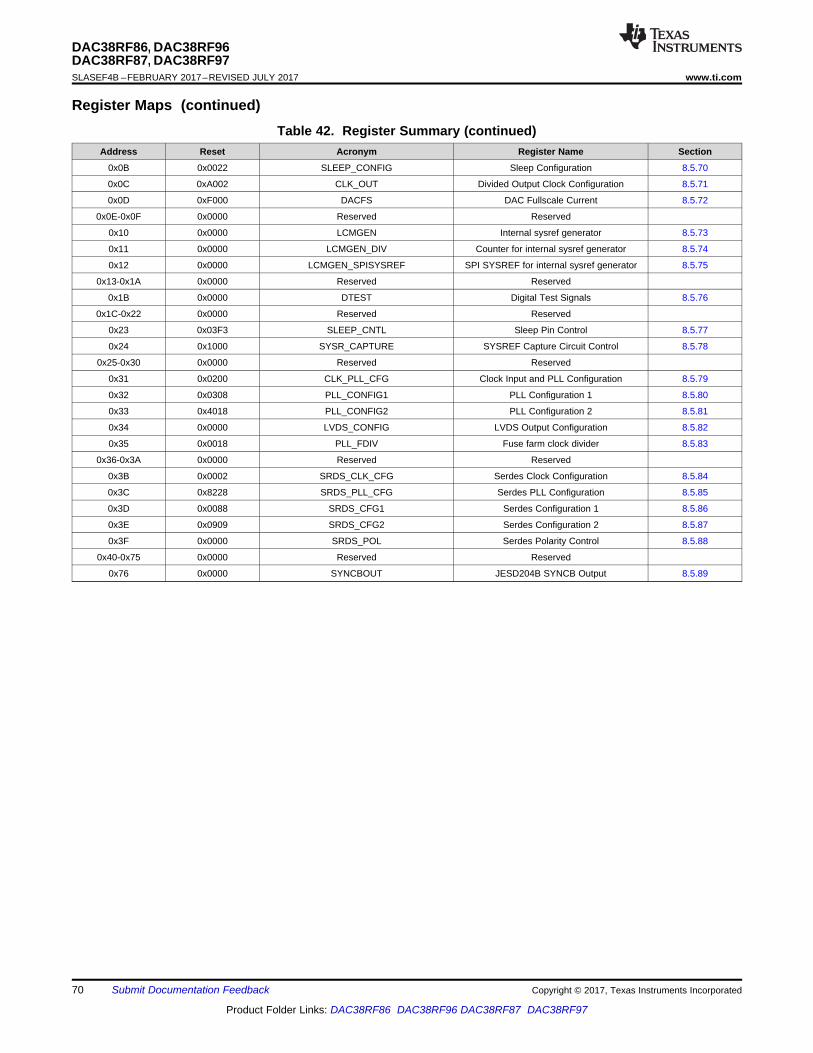
70
DAC38RF86, DAC38RF96DAC38RF87, DAC38RF97SLASEF4B –FEBRUARY 2017–REVISED JULY 2017 www.ti.com
Product Folder Links: DAC38RF86 DAC38RF96 DAC38RF87 DAC38RF97
Submit Documentation Feedback Copyright © 2017, Texas Instruments Incorporated
Register Maps (continued)Table 42. Register Summary (continued)
Address Reset Acronym Register Name Section
0x0B 0x0022 SLEEP_CONFIG Sleep Configuration 8.5.70
0x0C 0xA002 CLK_OUT Divided Output Clock Configuration 8.5.71
0x0D 0xF000 DACFS DAC Fullscale Current 8.5.72
0x0E-0x0F 0x0000 Reserved Reserved
0x10 0x0000 LCMGEN Internal sysref generator 8.5.73
0x11 0x0000 LCMGEN_DIV Counter for internal sysref generator 8.5.74
0x12 0x0000 LCMGEN_SPISYSREF SPI SYSREF for internal sysref generator 8.5.75
0x13-0x1A 0x0000 Reserved Reserved
0x1B 0x0000 DTEST Digital Test Signals 8.5.76
0x1C-0x22 0x0000 Reserved Reserved
0x23 0x03F3 SLEEP_CNTL Sleep Pin Control 8.5.77
0x24 0x1000 SYSR_CAPTURE SYSREF Capture Circuit Control 8.5.78
0x25-0x30 0x0000 Reserved Reserved
0x31 0x0200 CLK_PLL_CFG Clock Input and PLL Configuration 8.5.79
0x32 0x0308 PLL_CONFIG1 PLL Configuration 1 8.5.80
0x33 0x4018 PLL_CONFIG2 PLL Configuration 2 8.5.81
0x34 0x0000 LVDS_CONFIG LVDS Output Configuration 8.5.82
0x35 0x0018 PLL_FDIV Fuse farm clock divider 8.5.83
0x36-0x3A 0x0000 Reserved Reserved
0x3B 0x0002 SRDS_CLK_CFG Serdes Clock Configuration 8.5.84
0x3C 0x8228 SRDS_PLL_CFG Serdes PLL Configuration 8.5.85
0x3D 0x0088 SRDS_CFG1 Serdes Configuration 1 8.5.86
0x3E 0x0909 SRDS_CFG2 Serdes Configuration 2 8.5.87
0x3F 0x0000 SRDS_POL Serdes Polarity Control 8.5.88
0x40-0x75 0x0000 Reserved Reserved
0x76 0x0000 SYNCBOUT JESD204B SYNCB Output 8.5.89

71
DAC38RF86, DAC38RF96DAC38RF87, DAC38RF97
www.ti.com SLASEF4B –FEBRUARY 2017–REVISED JULY 2017
Product Folder Links: DAC38RF86 DAC38RF96 DAC38RF87 DAC38RF97
Submit Documentation FeedbackCopyright © 2017, Texas Instruments Incorporated
8.5.1 Chip Reset and Configuration Register (address = 0x00) [reset = 0x5803]
Figure 61. Chip Reset and Configuration Register (RESET_CONFIG)
15 14 13 12 11 10 9 80 0 0 0 0 0 0 x
RW RW RW RW RW RW RW RW
7 6 5 4 3 2 1 00 0 0 0 0 0 0 0
RW RW RW RW RW RW RW RWLEGEND: R/W = Read/Write; R = Read only; -n = value after reset
Table 43. RESET_CONFIG Field DescriptionsBit Field Type Reset Description15 SPI_RESET RW 0 This will reset all the SPI registers once programmed.14 ALM_OUT_POL RW 1 Changes the polarity of the alarm output.
0= active low1= active high
13 ALM_OUT_ENA RW 0 Turn on the alarm pin12 SYSCLK_ENA RW 1 Turns on the dividers for the SYSCLK to the Fusefarm11 AUTOLOAD_TRIG RW 1 Causes a Fuse AUTOLOAD to be executed.
10:7 Reserved RW 0000 Reserved6 ONE_DAC_ONLY RW 0 When set high only the SLICE0 is available.5 ONE_LINK_ONLY RW 0 This needs to be set high when a single link setup is being
programmed to get the correct TXENABLE signal generation4:2 Reserved RW 000 Reserved1 INIT_SLICE1 RW 1 Puts the multi-DAC2 JESD into initialization state0 INIT_SLICE0 RW 1 Puts the multi-DAC1 JESD into initialization state
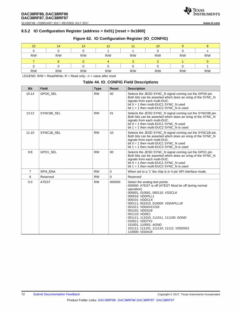
72
DAC38RF86, DAC38RF96DAC38RF87, DAC38RF97SLASEF4B –FEBRUARY 2017–REVISED JULY 2017 www.ti.com
Product Folder Links: DAC38RF86 DAC38RF96 DAC38RF87 DAC38RF97
Submit Documentation Feedback Copyright © 2017, Texas Instruments Incorporated
8.5.2 IO Configuration Register (address = 0x01) [reset = 0x1800]
Figure 62. IO Configuration Register (IO_CONFIG)
15 14 13 12 11 10 9 80 0 0 1 1 0 0 x
R/W R/W R/W R/W R/W R/W R/W R/W
7 6 5 4 3 2 1 00 0 0 0 0 0 0 1
R/W R/W R/W R/W R/W R/W R/W R/WLEGEND: R/W = Read/Write; R = Read only; -n = value after reset
Table 44. IO_CONFIG Field DescriptionsBit Field Type Reset Description
15:14 GPO0_SEL RW 00 Selects the JESD SYNC_N signal coming out the GPO0 pin.Both bits can be asserted which does an oring of the SYNC_Nsignals from each multi-DUC.bit 0 = 1 then multi-DUC1 SYNC_N usedbit 1 = 1 then multi-DUC2 SYNC_N is used
13:12 SYNC0B_SEL RW 01 Selects the JESD SYNC_N signal coming out the SYNC0B pin.Both bits can be asserted which does an oring of the SYNC_Nsignals from each multi-DUC.bit 0 = 1 then multi-DUC1 SYNC_N usedbit 1 = 1 then multi-DUC2 SYNC_N is used
11:10 SYNC1B_SEL RW 10 Selects the JESD SYNC_N signal coming out the SYNC1B pin.Both bits can be asserted which does an oring of the SYNC_Nsignals from each multi-DUC.bit 0 = 1 then multi-DUC1 SYNC_N usedbit 1 = 1 then multi-DUC2 SYNC_N is used
9:8 GPO1_SEL RW 00 Selects the JESD SYNC_N signal coming out the GPO1 pin.Both bits can be asserted which does an oring of the SYNC_Nsignals from each multi-DUC.bit 0 = 1 then multi-DUC1 SYNC_N usedbit 1 = 1 then multi-DUC2 SYNC_N is used
7 SPI4_ENA RW 0 When set to a '1' the chip is in 4 pin SPI interface mode.6 Reserved RW 0 Reserved
5:0 ATEST RW 000000 Select the analog test points:000000: ATEST is off (ATEST Must be off during normaloperation)000001, 010001, 000110: VSSCLK000010: VDDPLL1000101: VDDCLK000111, 001010, 010000: VDDAPLL18001011: VDDAVCO18001101: VDDS18001110: VDDE1001111, 111010, 111011, 111100: DGND010011: VDDTX1101001, 110001: AGND101111, 111101, 111110, 11111: VDDDIG1110000: VDDA18
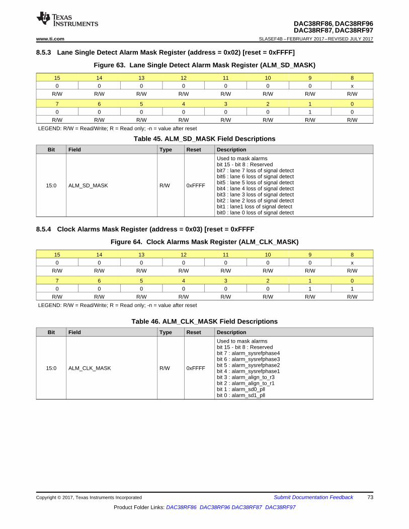
73
DAC38RF86, DAC38RF96DAC38RF87, DAC38RF97
www.ti.com SLASEF4B –FEBRUARY 2017–REVISED JULY 2017
Product Folder Links: DAC38RF86 DAC38RF96 DAC38RF87 DAC38RF97
Submit Documentation FeedbackCopyright © 2017, Texas Instruments Incorporated
8.5.3 Lane Single Detect Alarm Mask Register (address = 0x02) [reset = 0xFFFF]
Figure 63. Lane Single Detect Alarm Mask Register (ALM_SD_MASK)
15 14 13 12 11 10 9 80 0 0 0 0 0 0 x
R/W R/W R/W R/W R/W R/W R/W R/W
7 6 5 4 3 2 1 00 0 0 0 0 0 1 0
R/W R/W R/W R/W R/W R/W R/W R/WLEGEND: R/W = Read/Write; R = Read only; -n = value after reset
Table 45. ALM_SD_MASK Field DescriptionsBit Field Type Reset Description
15:0 ALM_SD_MASK R/W 0xFFFF
Used to mask alarmsbit 15 - bit 8 : Reservedbit7 : lane 7 loss of signal detectbit6 : lane 6 loss of signal detectbit5 : lane 5 loss of signal detectbit4 : lane 4 loss of signal detectbit3 : lane 3 loss of signal detectbit2 : lane 2 loss of signal detectbit1 : lane1 loss of signal detectbit0 : lane 0 loss of signal detect
8.5.4 Clock Alarms Mask Register (address = 0x03) [reset = 0xFFFF
Figure 64. Clock Alarms Mask Register (ALM_CLK_MASK)
15 14 13 12 11 10 9 80 0 0 0 0 0 0 x
R/W R/W R/W R/W R/W R/W R/W R/W
7 6 5 4 3 2 1 00 0 0 0 0 0 1 1
R/W R/W R/W R/W R/W R/W R/W R/WLEGEND: R/W = Read/Write; R = Read only; -n = value after reset
Table 46. ALM_CLK_MASK Field DescriptionsBit Field Type Reset Description
15:0 ALM_CLK_MASK R/W 0xFFFF
Used to mask alarmsbit 15 - bit 8 : Reservedbit 7 : alarm_sysrefphase4bit 6 : alarm_sysrefphase3bit 5 : alarm_sysrefphase2bit 4 : alarm_sysrefphase1bit 3 : alarm_align_to_r3bit 2 : alarm_align_to_r1bit 1 : alarm_sd0_pllbit 0 : alarm_sd1_pll
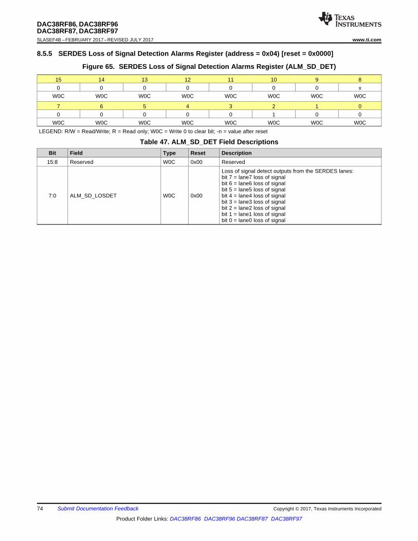
74
DAC38RF86, DAC38RF96DAC38RF87, DAC38RF97SLASEF4B –FEBRUARY 2017–REVISED JULY 2017 www.ti.com
Product Folder Links: DAC38RF86 DAC38RF96 DAC38RF87 DAC38RF97
Submit Documentation Feedback Copyright © 2017, Texas Instruments Incorporated
8.5.5 SERDES Loss of Signal Detection Alarms Register (address = 0x04) [reset = 0x0000]
Figure 65. SERDES Loss of Signal Detection Alarms Register (ALM_SD_DET)
15 14 13 12 11 10 9 80 0 0 0 0 0 0 x
W0C W0C W0C W0C W0C W0C W0C W0C
7 6 5 4 3 2 1 00 0 0 0 0 1 0 0
W0C W0C W0C W0C W0C W0C W0C W0CLEGEND: R/W = Read/Write; R = Read only; W0C = Write 0 to clear bit; -n = value after reset
Table 47. ALM_SD_DET Field DescriptionsBit Field Type Reset Description
15:8 Reserved W0C 0x00 Reserved
7:0 ALM_SD_LOSDET W0C 0x00
Loss of signal detect outputs from the SERDES lanes:bit 7 = lane7 loss of signalbit 6 = lane6 loss of signalbit 5 = lane5 loss of signalbit 4 = lane4 loss of signalbit 3 = lane3 loss of signalbit 2 = lane2 loss of signalbit 1 = lane1 loss of signalbit 0 = lane0 loss of signal
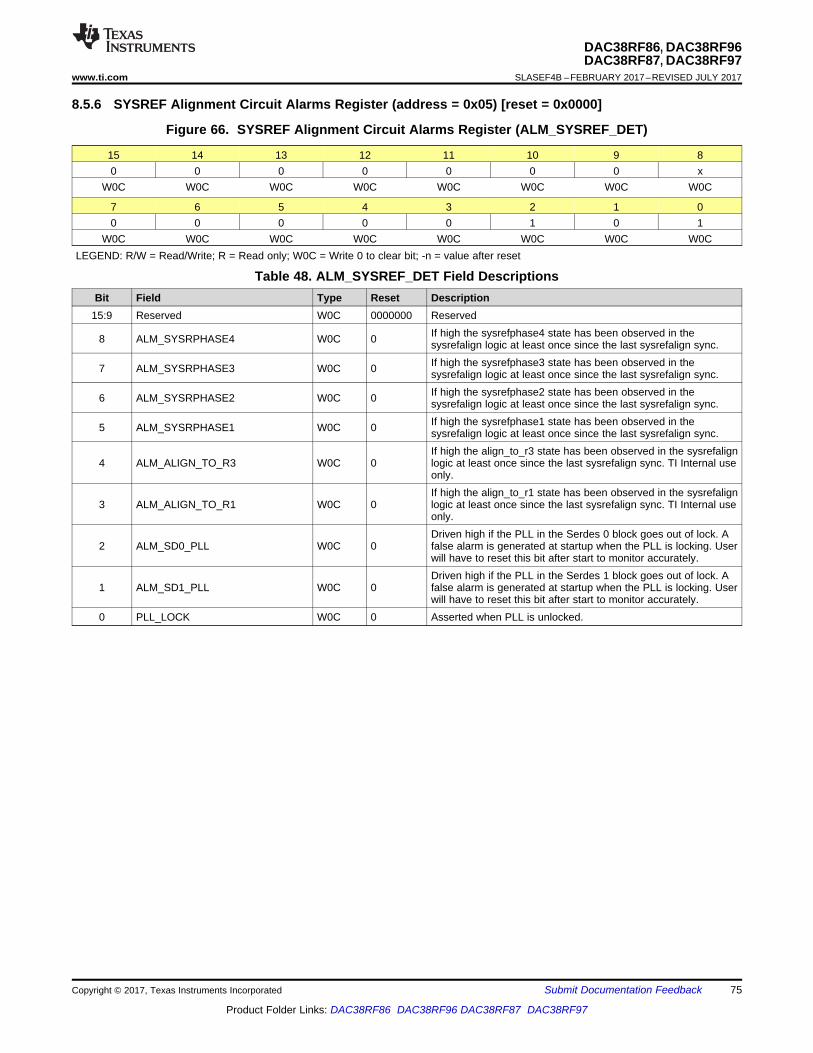
75
DAC38RF86, DAC38RF96DAC38RF87, DAC38RF97
www.ti.com SLASEF4B –FEBRUARY 2017–REVISED JULY 2017
Product Folder Links: DAC38RF86 DAC38RF96 DAC38RF87 DAC38RF97
Submit Documentation FeedbackCopyright © 2017, Texas Instruments Incorporated
8.5.6 SYSREF Alignment Circuit Alarms Register (address = 0x05) [reset = 0x0000]
Figure 66. SYSREF Alignment Circuit Alarms Register (ALM_SYSREF_DET)
15 14 13 12 11 10 9 80 0 0 0 0 0 0 x
W0C W0C W0C W0C W0C W0C W0C W0C
7 6 5 4 3 2 1 00 0 0 0 0 1 0 1
W0C W0C W0C W0C W0C W0C W0C W0CLEGEND: R/W = Read/Write; R = Read only; W0C = Write 0 to clear bit; -n = value after reset
Table 48. ALM_SYSREF_DET Field DescriptionsBit Field Type Reset Description
15:9 Reserved W0C 0000000 Reserved
8 ALM_SYSRPHASE4 W0C 0 If high the sysrefphase4 state has been observed in thesysrefalign logic at least once since the last sysrefalign sync.
7 ALM_SYSRPHASE3 W0C 0 If high the sysrefphase3 state has been observed in thesysrefalign logic at least once since the last sysrefalign sync.
6 ALM_SYSRPHASE2 W0C 0 If high the sysrefphase2 state has been observed in thesysrefalign logic at least once since the last sysrefalign sync.
5 ALM_SYSRPHASE1 W0C 0 If high the sysrefphase1 state has been observed in thesysrefalign logic at least once since the last sysrefalign sync.
4 ALM_ALIGN_TO_R3 W0C 0If high the align_to_r3 state has been observed in the sysrefalignlogic at least once since the last sysrefalign sync. TI Internal useonly.
3 ALM_ALIGN_TO_R1 W0C 0If high the align_to_r1 state has been observed in the sysrefalignlogic at least once since the last sysrefalign sync. TI Internal useonly.
2 ALM_SD0_PLL W0C 0Driven high if the PLL in the Serdes 0 block goes out of lock. Afalse alarm is generated at startup when the PLL is locking. Userwill have to reset this bit after start to monitor accurately.
1 ALM_SD1_PLL W0C 0Driven high if the PLL in the Serdes 1 block goes out of lock. Afalse alarm is generated at startup when the PLL is locking. Userwill have to reset this bit after start to monitor accurately.
0 PLL_LOCK W0C 0 Asserted when PLL is unlocked.
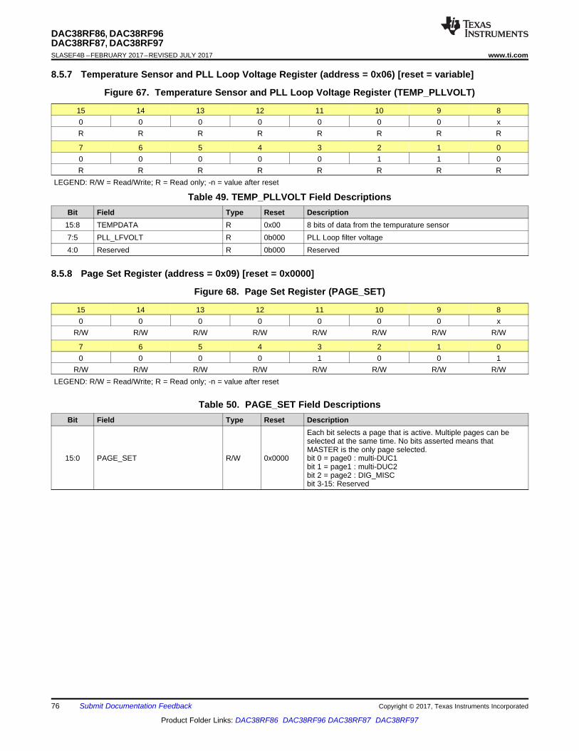
76
DAC38RF86, DAC38RF96DAC38RF87, DAC38RF97SLASEF4B –FEBRUARY 2017–REVISED JULY 2017 www.ti.com
Product Folder Links: DAC38RF86 DAC38RF96 DAC38RF87 DAC38RF97
Submit Documentation Feedback Copyright © 2017, Texas Instruments Incorporated
8.5.7 Temperature Sensor and PLL Loop Voltage Register (address = 0x06) [reset = variable]
Figure 67. Temperature Sensor and PLL Loop Voltage Register (TEMP_PLLVOLT)
15 14 13 12 11 10 9 80 0 0 0 0 0 0 xR R R R R R R R
7 6 5 4 3 2 1 00 0 0 0 0 1 1 0R R R R R R R R
LEGEND: R/W = Read/Write; R = Read only; -n = value after reset
Table 49. TEMP_PLLVOLT Field DescriptionsBit Field Type Reset Description
15:8 TEMPDATA R 0x00 8 bits of data from the tempurature sensor7:5 PLL_LFVOLT R 0b000 PLL Loop filter voltage4:0 Reserved R 0b000 Reserved
8.5.8 Page Set Register (address = 0x09) [reset = 0x0000]
Figure 68. Page Set Register (PAGE_SET)
15 14 13 12 11 10 9 80 0 0 0 0 0 0 x
R/W R/W R/W R/W R/W R/W R/W R/W
7 6 5 4 3 2 1 00 0 0 0 1 0 0 1
R/W R/W R/W R/W R/W R/W R/W R/WLEGEND: R/W = Read/Write; R = Read only; -n = value after reset
Table 50. PAGE_SET Field DescriptionsBit Field Type Reset Description
15:0 PAGE_SET R/W 0x0000
Each bit selects a page that is active. Multiple pages can beselected at the same time. No bits asserted means thatMASTER is the only page selected.bit 0 = page0 : multi-DUC1bit 1 = page1 : multi-DUC2bit 2 = page2 : DIG_MISCbit 3-15: Reserved
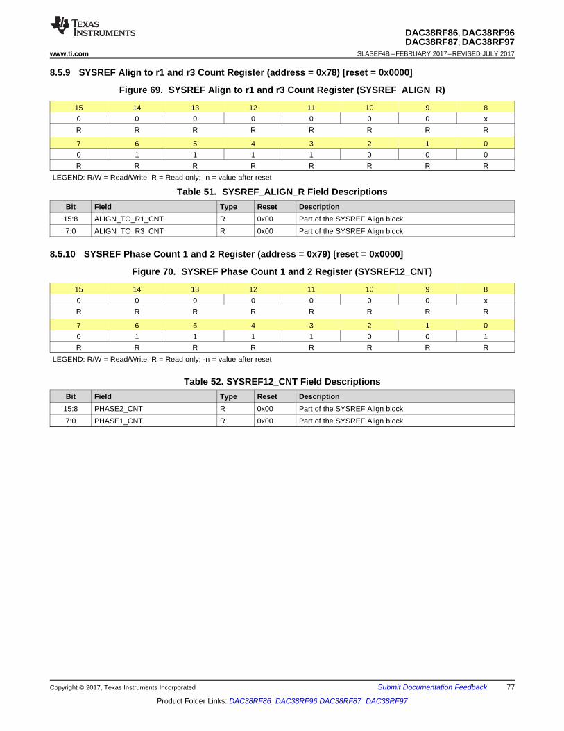
77
DAC38RF86, DAC38RF96DAC38RF87, DAC38RF97
www.ti.com SLASEF4B –FEBRUARY 2017–REVISED JULY 2017
Product Folder Links: DAC38RF86 DAC38RF96 DAC38RF87 DAC38RF97
Submit Documentation FeedbackCopyright © 2017, Texas Instruments Incorporated
8.5.9 SYSREF Align to r1 and r3 Count Register (address = 0x78) [reset = 0x0000]
Figure 69. SYSREF Align to r1 and r3 Count Register (SYSREF_ALIGN_R)
15 14 13 12 11 10 9 80 0 0 0 0 0 0 xR R R R R R R R
7 6 5 4 3 2 1 00 1 1 1 1 0 0 0R R R R R R R R
LEGEND: R/W = Read/Write; R = Read only; -n = value after reset
Table 51. SYSREF_ALIGN_R Field DescriptionsBit Field Type Reset Description
15:8 ALIGN_TO_R1_CNT R 0x00 Part of the SYSREF Align block7:0 ALIGN_TO_R3_CNT R 0x00 Part of the SYSREF Align block
8.5.10 SYSREF Phase Count 1 and 2 Register (address = 0x79) [reset = 0x0000]
Figure 70. SYSREF Phase Count 1 and 2 Register (SYSREF12_CNT)
15 14 13 12 11 10 9 80 0 0 0 0 0 0 xR R R R R R R R
7 6 5 4 3 2 1 00 1 1 1 1 0 0 1R R R R R R R R
LEGEND: R/W = Read/Write; R = Read only; -n = value after reset
Table 52. SYSREF12_CNT Field DescriptionsBit Field Type Reset Description
15:8 PHASE2_CNT R 0x00 Part of the SYSREF Align block7:0 PHASE1_CNT R 0x00 Part of the SYSREF Align block
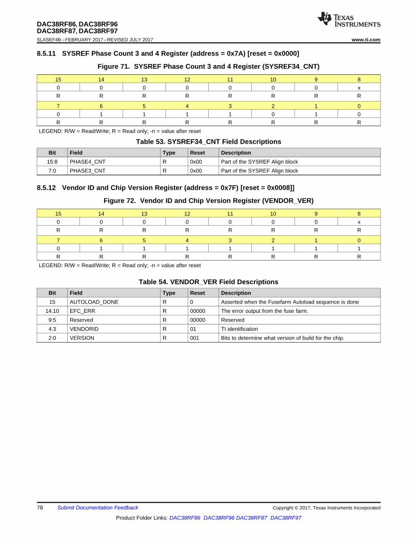
78
DAC38RF86, DAC38RF96DAC38RF87, DAC38RF97SLASEF4B –FEBRUARY 2017–REVISED JULY 2017 www.ti.com
Product Folder Links: DAC38RF86 DAC38RF96 DAC38RF87 DAC38RF97
Submit Documentation Feedback Copyright © 2017, Texas Instruments Incorporated
8.5.11 SYSREF Phase Count 3 and 4 Register (address = 0x7A) [reset = 0x0000]
Figure 71. SYSREF Phase Count 3 and 4 Register (SYSREF34_CNT)
15 14 13 12 11 10 9 80 0 0 0 0 0 0 xR R R R R R R R
7 6 5 4 3 2 1 00 1 1 1 1 0 1 0R R R R R R R R
LEGEND: R/W = Read/Write; R = Read only; -n = value after reset
Table 53. SYSREF34_CNT Field DescriptionsBit Field Type Reset Description
15:8 PHASE4_CNT R 0x00 Part of the SYSREF Align block7:0 PHASE3_CNT R 0x00 Part of the SYSREF Align block
8.5.12 Vendor ID and Chip Version Register (address = 0x7F) [reset = 0x0008]]
Figure 72. Vendor ID and Chip Version Register (VENDOR_VER)
15 14 13 12 11 10 9 80 0 0 0 0 0 0 xR R R R R R R R
7 6 5 4 3 2 1 00 1 1 1 1 1 1 1R R R R R R R R
LEGEND: R/W = Read/Write; R = Read only; -n = value after reset
Table 54. VENDOR_VER Field DescriptionsBit Field Type Reset Description15 AUTOLOAD_DONE R 0 Asserted when the Fusefarm Autoload sequence is done
14:10 EFC_ERR R 00000 The error output from the fuse farm.9:5 Reserved R 00000 Reserved4:3 VENDORID R 01 TI identification2:0 VERSION R 001 Bits to determine what version of build for the chip.

79
DAC38RF86, DAC38RF96DAC38RF87, DAC38RF97
www.ti.com SLASEF4B –FEBRUARY 2017–REVISED JULY 2017
Product Folder Links: DAC38RF86 DAC38RF96 DAC38RF87 DAC38RF97
Submit Documentation FeedbackCopyright © 2017, Texas Instruments Incorporated
8.5.13 Multi-DUC Configuration (PAP, Interpolation) Register (address = 0x0A) [reset = 0x02B0]
Figure 73. Multi-DUC Configuration (PAP, Interolation) Register (MULTIDUC_CFG1)
15 14 13 12 11 10 9 80 0 0 0 0 0 0 x
R/W R/W R/W R/W R/W R/W R/W R/W
7 6 5 4 3 2 1 01 0 0 0 1 0 1 0
R/W R/W R/W R/W R/W R/W R/W R/WLEGEND: R/W = Read/Write; R = Read only; -n = value after reset
Table 55. MULTIDUC_CFG1 Field DescriptionsBit Field Type Reset Description15 DUAL_IQ R/W 0 When asserted the SLICE uses both IQ paths14 ISFIR_ENA R/W 0 Turns on the inverse sync filter for the AB and CD paths when
programmed to 1.13 Not used R/W 0 Not used
12:8 INTERP R/W 00010 Determines the interpolation amount.00000: 1x00001: 2x00010: 4x00011: 6x00100: 8x00101: 10x00110: 12x01000: 16x01001: 18x01010: 20x01100: 24x
7 ALM_ZEROS_TXEN R/W 1 When asserted any alarm that isn’t masked will mid-level theDAC output by setting the txenable_from_dig to ‘0’
6 DAC_COMPLEMENT R/W 0 When asserted the DAC output will be 2's complemented. Thishelps with hookup at the board level.
5 ALM_ZEROS_JESD R/W 1 When asserted any alarm that isn’t masked will zero the datacoming out of the JESD block.
4 ALM_OUT_ENA R/W 1 When asserted the output from the selected SLICE will bepassed on to the MASTER alarm control if it is also turned onthen the alarm will be sent to the pad_alarm pin.
3 PAPA_ENA R/W 0 Turns on the Power Amp Protection logic for path A.2 PAPB_ENA R/W 0 Turns on the Power Amp Protection logic for path B.1 PAPC_ENA R/W 0 Turns on the Power Amp Protection logic for path C.0 PAPD_ENA R/W 0 Turns on the Power Amp Protection logic for path D.

80
DAC38RF86, DAC38RF96DAC38RF87, DAC38RF97SLASEF4B –FEBRUARY 2017–REVISED JULY 2017 www.ti.com
Product Folder Links: DAC38RF86 DAC38RF96 DAC38RF87 DAC38RF97
Submit Documentation Feedback Copyright © 2017, Texas Instruments Incorporated
8.5.14 Multi-DUC Configuration (Mixers) Register (address = 0x0C) [reset = 0x2402]
Figure 74. Multi-DUC Configuration (Mixers) Register (MULTIDUC_CFG2)
15 14 13 12 11 10 9 80 0 0 0 0 1 0 x
R/W R/W R/W R/W R/W R/W R/W R/W
7 6 5 4 3 2 1 00 0 0 0 1 1 0 0
R/W R/W R/W R/W R/W R/W R/W R/WLEGEND: R/W = Read/Write; R = Read only; -n = value after reset
Table 56. MULTIDUC_CFG2 Field DescriptionsBit Field Type Reset Description
15:14 DAC_BITWIDTH R/W 0b00 Determines the bit width of the data going to the DAC00: 14 bits01: 14 bits10: 12 bits11: 11 bits
13 ZERO_INVLD_DATA R/W 1 When asserted; the data from the JESD block is zeroed in themapper to prevent goofy output from the DAC. For test purposesthis bit should be desasserted
12 SHORTTEST_ENA R/W 0 Turns on the JESD SHORT pattern test (5.1.6.2)11 Reserved R/W 0 Reserved10 Reserved R/W 1 Reserved9 MIXERAB_ENA R/W 0 Turns on the mixer for the A and B streams8 MIXERCD_ENA R/W 0 Turns on the mixer for the C and D streams7 MIXERAB_GAIN R/W 0 Adds 6dB of gain when asserted6 MIXERCD_GAIN R/W 0 Adds 6dB of gain when asserted5 NCOAB_ENA R/W 0 When high the full NCO block is turned on.4 NCOCD_ENA R/W 0 When high the full NCO block is turned on.
3:2 Reserved R/W 00 Reserved1 TWOS R/W 1 When asserted the chip is expecting 2's complement data is
arriving through the JESD; otherwise offset binary is expected0 Reserved R/W 0 Reserved
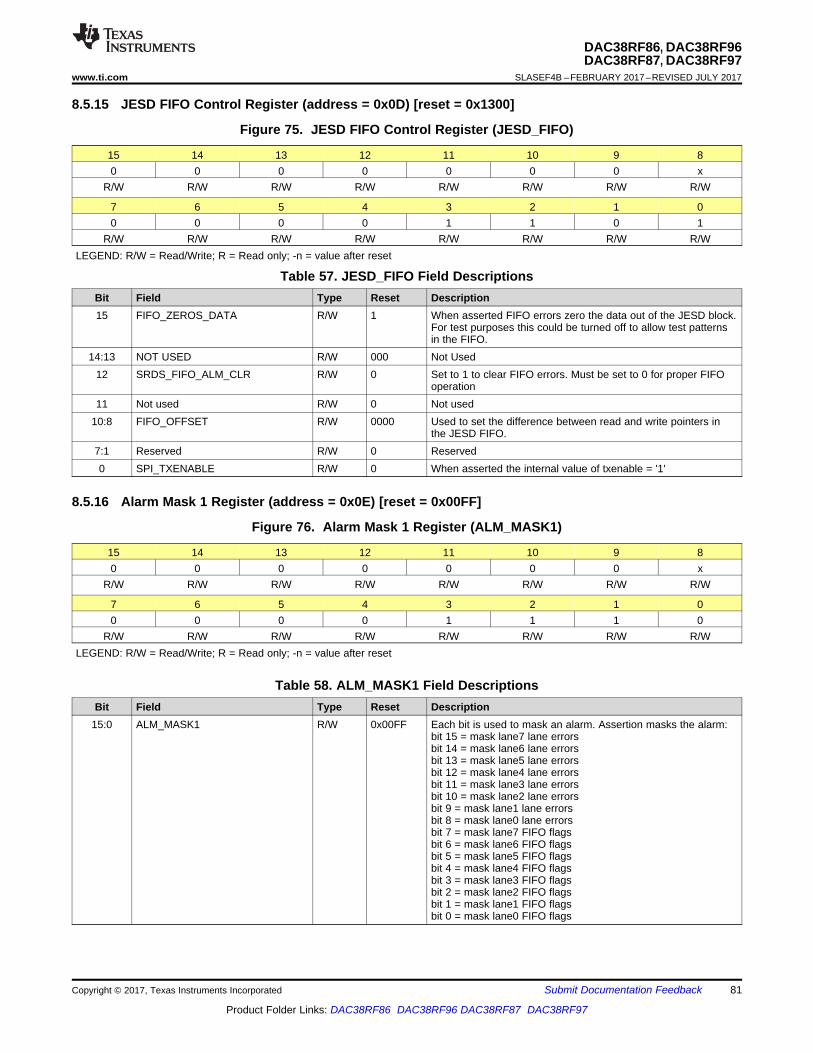
81
DAC38RF86, DAC38RF96DAC38RF87, DAC38RF97
www.ti.com SLASEF4B –FEBRUARY 2017–REVISED JULY 2017
Product Folder Links: DAC38RF86 DAC38RF96 DAC38RF87 DAC38RF97
Submit Documentation FeedbackCopyright © 2017, Texas Instruments Incorporated
8.5.15 JESD FIFO Control Register (address = 0x0D) [reset = 0x1300]
Figure 75. JESD FIFO Control Register (JESD_FIFO)
15 14 13 12 11 10 9 80 0 0 0 0 0 0 x
R/W R/W R/W R/W R/W R/W R/W R/W
7 6 5 4 3 2 1 00 0 0 0 1 1 0 1
R/W R/W R/W R/W R/W R/W R/W R/WLEGEND: R/W = Read/Write; R = Read only; -n = value after reset
Table 57. JESD_FIFO Field DescriptionsBit Field Type Reset Description15 FIFO_ZEROS_DATA R/W 1 When asserted FIFO errors zero the data out of the JESD block.
For test purposes this could be turned off to allow test patternsin the FIFO.
14:13 NOT USED R/W 000 Not Used12 SRDS_FIFO_ALM_CLR R/W 0 Set to 1 to clear FIFO errors. Must be set to 0 for proper FIFO
operation11 Not used R/W 0 Not used
10:8 FIFO_OFFSET R/W 0000 Used to set the difference between read and write pointers inthe JESD FIFO.
7:1 Reserved R/W 0 Reserved0 SPI_TXENABLE R/W 0 When asserted the internal value of txenable = '1'
8.5.16 Alarm Mask 1 Register (address = 0x0E) [reset = 0x00FF]
Figure 76. Alarm Mask 1 Register (ALM_MASK1)
15 14 13 12 11 10 9 80 0 0 0 0 0 0 x
R/W R/W R/W R/W R/W R/W R/W R/W
7 6 5 4 3 2 1 00 0 0 0 1 1 1 0
R/W R/W R/W R/W R/W R/W R/W R/WLEGEND: R/W = Read/Write; R = Read only; -n = value after reset
Table 58. ALM_MASK1 Field DescriptionsBit Field Type Reset Description
15:0 ALM_MASK1 R/W 0x00FF Each bit is used to mask an alarm. Assertion masks the alarm:bit 15 = mask lane7 lane errorsbit 14 = mask lane6 lane errorsbit 13 = mask lane5 lane errorsbit 12 = mask lane4 lane errorsbit 11 = mask lane3 lane errorsbit 10 = mask lane2 lane errorsbit 9 = mask lane1 lane errorsbit 8 = mask lane0 lane errorsbit 7 = mask lane7 FIFO flagsbit 6 = mask lane6 FIFO flagsbit 5 = mask lane5 FIFO flagsbit 4 = mask lane4 FIFO flagsbit 3 = mask lane3 FIFO flagsbit 2 = mask lane2 FIFO flagsbit 1 = mask lane1 FIFO flagsbit 0 = mask lane0 FIFO flags
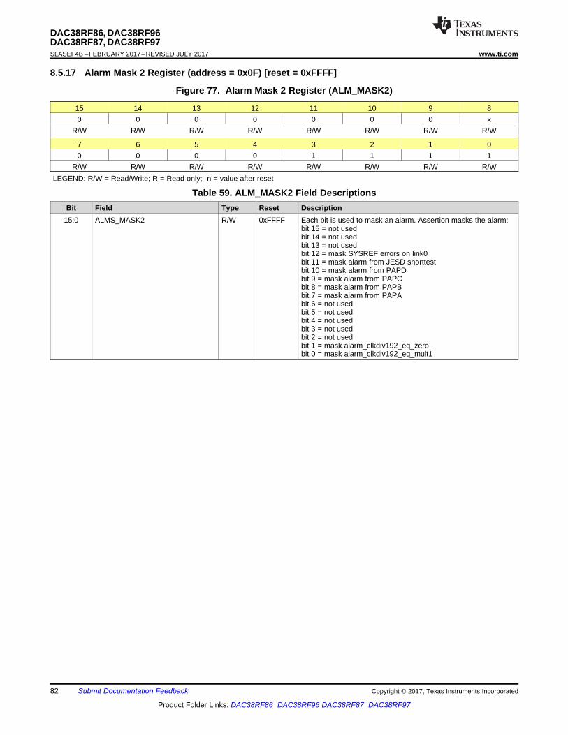
82
DAC38RF86, DAC38RF96DAC38RF87, DAC38RF97SLASEF4B –FEBRUARY 2017–REVISED JULY 2017 www.ti.com
Product Folder Links: DAC38RF86 DAC38RF96 DAC38RF87 DAC38RF97
Submit Documentation Feedback Copyright © 2017, Texas Instruments Incorporated
8.5.17 Alarm Mask 2 Register (address = 0x0F) [reset = 0xFFFF]
Figure 77. Alarm Mask 2 Register (ALM_MASK2)
15 14 13 12 11 10 9 80 0 0 0 0 0 0 x
R/W R/W R/W R/W R/W R/W R/W R/W
7 6 5 4 3 2 1 00 0 0 0 1 1 1 1
R/W R/W R/W R/W R/W R/W R/W R/WLEGEND: R/W = Read/Write; R = Read only; -n = value after reset
Table 59. ALM_MASK2 Field DescriptionsBit Field Type Reset Description
15:0 ALMS_MASK2 R/W 0xFFFF Each bit is used to mask an alarm. Assertion masks the alarm:bit 15 = not usedbit 14 = not usedbit 13 = not usedbit 12 = mask SYSREF errors on link0bit 11 = mask alarm from JESD shorttestbit 10 = mask alarm from PAPDbit 9 = mask alarm from PAPCbit 8 = mask alarm from PAPBbit 7 = mask alarm from PAPAbit 6 = not usedbit 5 = not usedbit 4 = not usedbit 3 = not usedbit 2 = not usedbit 1 = mask alarm_clkdiv192_eq_zerobit 0 = mask alarm_clkdiv192_eq_mult1
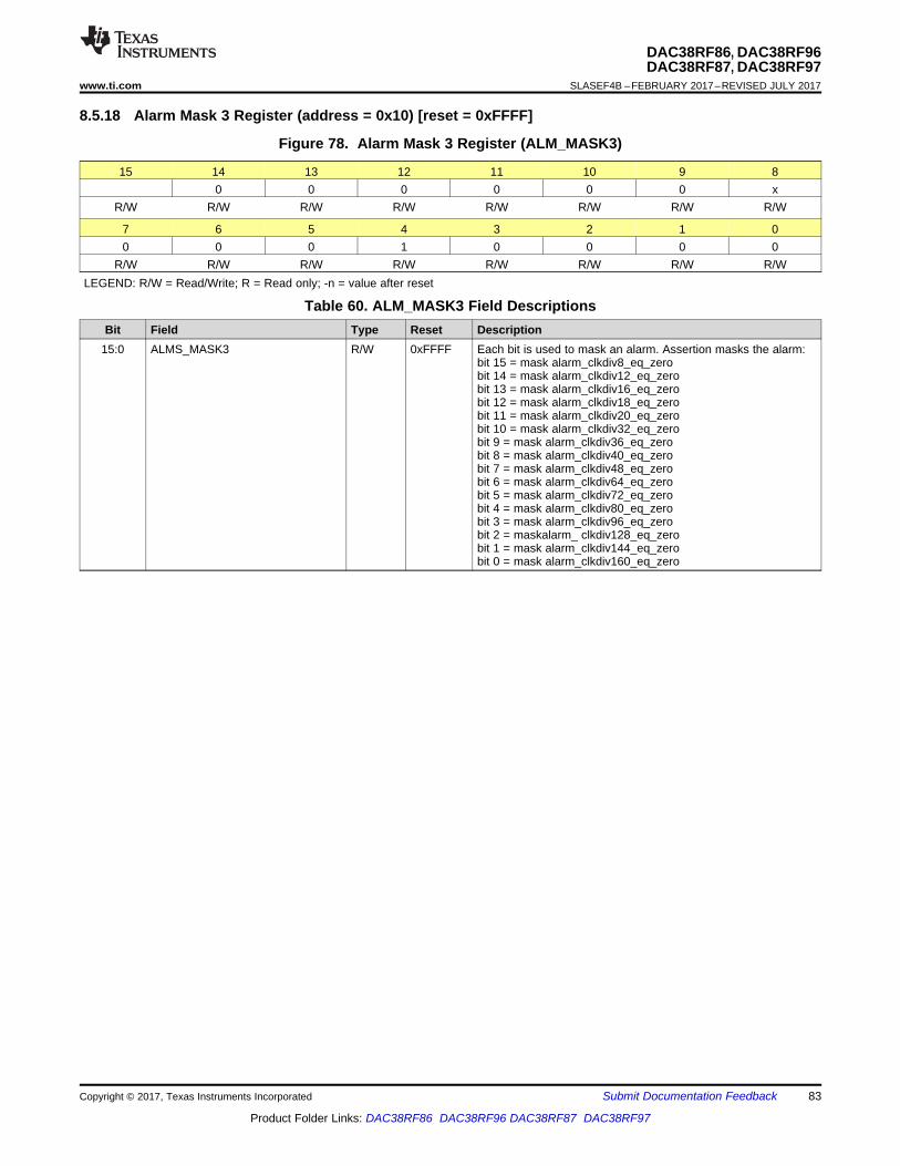
83
DAC38RF86, DAC38RF96DAC38RF87, DAC38RF97
www.ti.com SLASEF4B –FEBRUARY 2017–REVISED JULY 2017
Product Folder Links: DAC38RF86 DAC38RF96 DAC38RF87 DAC38RF97
Submit Documentation FeedbackCopyright © 2017, Texas Instruments Incorporated
8.5.18 Alarm Mask 3 Register (address = 0x10) [reset = 0xFFFF]
Figure 78. Alarm Mask 3 Register (ALM_MASK3)
15 14 13 12 11 10 9 80 0 0 0 0 0 x
R/W R/W R/W R/W R/W R/W R/W R/W
7 6 5 4 3 2 1 00 0 0 1 0 0 0 0
R/W R/W R/W R/W R/W R/W R/W R/WLEGEND: R/W = Read/Write; R = Read only; -n = value after reset
Table 60. ALM_MASK3 Field DescriptionsBit Field Type Reset Description
15:0 ALMS_MASK3 R/W 0xFFFF Each bit is used to mask an alarm. Assertion masks the alarm:bit 15 = mask alarm_clkdiv8_eq_zerobit 14 = mask alarm_clkdiv12_eq_zerobit 13 = mask alarm_clkdiv16_eq_zerobit 12 = mask alarm_clkdiv18_eq_zerobit 11 = mask alarm_clkdiv20_eq_zerobit 10 = mask alarm_clkdiv32_eq_zerobit 9 = mask alarm_clkdiv36_eq_zerobit 8 = mask alarm_clkdiv40_eq_zerobit 7 = mask alarm_clkdiv48_eq_zerobit 6 = mask alarm_clkdiv64_eq_zerobit 5 = mask alarm_clkdiv72_eq_zerobit 4 = mask alarm_clkdiv80_eq_zerobit 3 = mask alarm_clkdiv96_eq_zerobit 2 = maskalarm_ clkdiv128_eq_zerobit 1 = mask alarm_clkdiv144_eq_zerobit 0 = mask alarm_clkdiv160_eq_zero

84
DAC38RF86, DAC38RF96DAC38RF87, DAC38RF97SLASEF4B –FEBRUARY 2017–REVISED JULY 2017 www.ti.com
Product Folder Links: DAC38RF86 DAC38RF96 DAC38RF87 DAC38RF97
Submit Documentation Feedback Copyright © 2017, Texas Instruments Incorporated
8.5.19 Alarm Mask 4 Register (address = 0x11) [reset = 0xFFFF]
Figure 79. Alarm Mask 4 Register (ALM_MASK4)
15 14 13 12 11 10 9 80 0 0 0 0 0 0 x
R/W R/W R/W R/W R/W R/W R/W R/W
7 6 5 4 3 2 1 00 0 0 1 0 0 0 1
R/W R/W R/W R/W R/W R/W R/W R/WLEGEND: R/W = Read/Write; R = Read only; -n = value after reset
Table 61. ALM_MASK4 Field DescriptionsBit Field Type Reset Description
15:0 ALMS_MASK4 R/W 0xFFFF Each bit is used to mask an alarm. Assertion masks the alarm:bit 15 = mask alarm_clkdiv8_eq_mult1bit 14 = mask alarm_clkdiv12_eq_mult1bit 13 = mask alarm_clkdiv16_eq_mult1bit 12 = mask alarm_clkdiv18_eq_mult1bit 11 = mask alarm_clkdiv20_eq_mult1bit 10 = mask alarm_clkdiv32_eq_mult1bit 9 = mask alarm_clkdiv36_eq_mult1bit 8 = mask alarm_clkdiv40_eq_mult1bit 7 = mask alarm_clkdiv48_eq_mult1bit 6 = mask alarm_clkdiv64_eq_mult1bit 5 = mask alarm_clkdiv72_eq_mult1bit 4 = mask alarm_clkdiv80_eq_mult1bit 3 = mask alarm_clkdiv96_eq_mult1bit 2 = maskalarm_ clkdiv128_eq_mult1bit 1 = mask alarm_clkdiv144_eq_mult1bit 0 = mask alarm_clkdiv160_eq_mult1
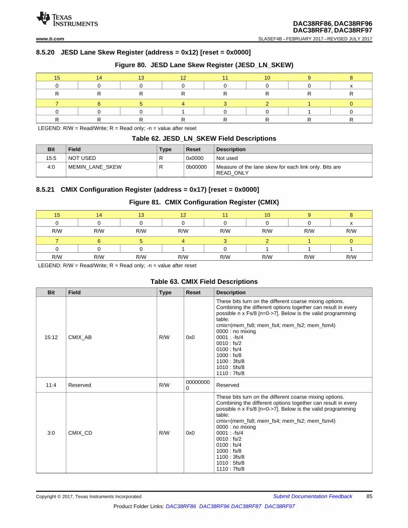
85
DAC38RF86, DAC38RF96DAC38RF87, DAC38RF97
www.ti.com SLASEF4B –FEBRUARY 2017–REVISED JULY 2017
Product Folder Links: DAC38RF86 DAC38RF96 DAC38RF87 DAC38RF97
Submit Documentation FeedbackCopyright © 2017, Texas Instruments Incorporated
8.5.20 JESD Lane Skew Register (address = 0x12) [reset = 0x0000]
Figure 80. JESD Lane Skew Register (JESD_LN_SKEW)
15 14 13 12 11 10 9 80 0 0 0 0 0 0 xR R R R R R R R
7 6 5 4 3 2 1 00 0 0 1 0 0 1 0R R R R R R R R
LEGEND: R/W = Read/Write; R = Read only; -n = value after reset
Table 62. JESD_LN_SKEW Field DescriptionsBit Field Type Reset Description
15:5 NOT USED R 0x0000 Not used4:0 MEMIN_LANE_SKEW R 0b00000 Measure of the lane skew for each link only. Bits are
READ_ONLY
8.5.21 CMIX Configuration Register (address = 0x17) [reset = 0x0000]
Figure 81. CMIX Configuration Register (CMIX)
15 14 13 12 11 10 9 80 0 0 0 0 0 0 x
R/W R/W R/W R/W R/W R/W R/W R/W
7 6 5 4 3 2 1 00 0 0 1 0 1 1 1
R/W R/W R/W R/W R/W R/W R/W R/WLEGEND: R/W = Read/Write; R = Read only; -n = value after reset
Table 63. CMIX Field DescriptionsBit Field Type Reset Description
15:12 CMIX_AB R/W 0x0
These bits turn on the different coarse mixing options.Combining the different options together can result in everypossible n x Fs/8 [n=0->7]. Below is the valid programmingtable:cmix=(mem_fs8; mem_fs4; mem_fs2; mem_fsm4)0000 : no mixing0001 : -fs/40010 : fs/20100 : fs/41000 : fs/81100 : 3fs/81010 : 5fs/81110 : 7fs/8
11:4 Reserved R/W 000000000 Reserved
3:0 CMIX_CD R/W 0x0
These bits turn on the different coarse mixing options.Combining the different options together can result in everypossible n x Fs/8 [n=0->7]. Below is the valid programmingtable:cmix=(mem_fs8; mem_fs4; mem_fs2; mem_fsm4)0000 : no mixing0001 : -fs/40010 : fs/20100 : fs/41000 : fs/81100 : 3fs/81010 : 5fs/81110 : 7fs/8

86
DAC38RF86, DAC38RF96DAC38RF87, DAC38RF97SLASEF4B –FEBRUARY 2017–REVISED JULY 2017 www.ti.com
Product Folder Links: DAC38RF86 DAC38RF96 DAC38RF87 DAC38RF97
Submit Documentation Feedback Copyright © 2017, Texas Instruments Incorporated
8.5.22 Output Summation and Delay Register (address = 0x19) [reset = 0x0000]
Figure 82. Output Summation and Delay Register (OUTSUM)
15 14 13 12 11 10 9 80 0 0 0 0 0 0 x
R/W R/W R/W R/W R/W R/W R/W R/W
7 6 5 4 3 2 1 00 0 0 1 1 0 0 1
R/W R/W R/W R/W R/W R/W R/W R/WLEGEND: R/W = Read/Write; R = Read only; -n = value after reset
Table 64. OUTSUM Field DescriptionsBit Field Type Reset Description
15:12 OUTPUT_DELAY R/W 0x0 Delays the output to the DAC 0 to 15 clock cycles11:4 Reserved R/W 0x00 Reserved
3:0 OUTSUM_SEL R/W 0x0
Selects the output summing functions. Each bit selects anothersample to sum. Multiple bits can be selected.bit 0 = add the path AB samplebit 1 = add the path CD samplebit 2 = add adjacent DAC path AB samplebit 3 = add adjacent DAC path CD sample
8.5.23 NCO Phase Path AB Register (address = 0x1C) [reset = 0x0000]
Figure 83. NCO Phase Path AB Register (PHASE_NCOAB)
15 14 13 12 11 10 9 80 0 0 0 0 0 0 x
R/W R/W R/W R/W R/W R/W R/W R/W
7 6 5 4 3 2 1 00 0 0 1 1 1 0 0
R/W R/W R/W R/W R/W R/W R/W R/WLEGEND: R/W = Read/Write; R = Read only; -n = value after reset
Table 65. PHASE_NCOAB Field DescriptionsBit Field Type Reset Description
15:0 PHASE_NCO1 AutoSync
0x0000 The phase offset for the FULL NCO1 in the AB datapath.
8.5.24 NCO Phase Path CD Register (address = 0x1D) [reset = 0x0000]
Figure 84. NCO Phase Path CD Register (PHASE_NCOCD)
15 14 13 12 11 10 9 80 0 0 0 0 0 0 0
R/W R/W R/W R/W R/W R/W R/W R/W
7 6 5 4 3 2 1 00 0 0 1 1 1 0 1
R/W R/W R/W R/W R/W R/W R/W R/WLEGEND: R/W = Read/Write; R = Read only; -n = value after reset
Table 66. PHASE_NCOCD Field DescriptionsBit Field Type Reset Description
15:0 PHASE_NCO12 AutoSync
0x0000 The phase offset for the FULL NCO2 in the CD datapath.
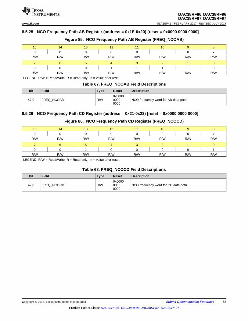
87
DAC38RF86, DAC38RF96DAC38RF87, DAC38RF97
www.ti.com SLASEF4B –FEBRUARY 2017–REVISED JULY 2017
Product Folder Links: DAC38RF86 DAC38RF96 DAC38RF87 DAC38RF97
Submit Documentation FeedbackCopyright © 2017, Texas Instruments Incorporated
8.5.25 NCO Frequency Path AB Register (address = 0x1E-0x20) [reset = 0x0000 0000 0000]
Figure 85. NCO Frequency Path AB Register (FREQ_NCOAB)
15 14 13 12 11 10 9 80 0 0 0 0 0 0 x
R/W R/W R/W R/W R/W R/W R/W R/W
7 6 5 4 3 2 1 00 0 0 1 1 1 1 0
R/W R/W R/W R/W R/W R/W R/W R/WLEGEND: R/W = Read/Write; R = Read only; -n = value after reset
Table 67. FREQ_NCOAB Field DescriptionsBit Field Type Reset Description
47:0 FREQ_NCOAB R/W0x000000000000
NCO frequency word for AB data path.
8.5.26 NCO Frequency Path CD Register (address = 0x21-0x23) [reset = 0x0000 0000 0000]
Figure 86. NCO Frequency Path CD Register (FREQ_NCOCD)
15 14 13 12 11 10 9 80 0 0 0 0 0 0 x
R/W R/W R/W R/W R/W R/W R/W R/W
7 6 5 4 3 2 1 00 0 1 0 0 0 0 1
R/W R/W R/W R/W R/W R/W R/W R/WLEGEND: R/W = Read/Write; R = Read only; -n = value after reset
Table 68. FREQ_NCOCD Field DescriptionsBit Field Type Reset Description
47:0 FREQ_NCOCD R/W0x000000000000
NCO frequency word for CD data path.

88
DAC38RF86, DAC38RF96DAC38RF87, DAC38RF97SLASEF4B –FEBRUARY 2017–REVISED JULY 2017 www.ti.com
Product Folder Links: DAC38RF86 DAC38RF96 DAC38RF87 DAC38RF97
Submit Documentation Feedback Copyright © 2017, Texas Instruments Incorporated
8.5.27 SYSREF Use for Clock Divider Register (address = 0x24) [reset = 0x0010]
Figure 87. SYSREF Use for Clock Divder Register (SYSREF_CLKDIV)
15 14 13 12 11 10 9 80 0 0 0 0 0 0 x
R/W R/W R/W R/W R/W R/W R/W R/W
7 6 5 4 3 2 1 00 0 1 0 0 1 0 0
R/W R/W R/W R/W R/W R/W R/W R/WLEGEND: R/W = Read/Write; R = Read only; -n = value after reset
Table 69. SYSREF_CLKDIV Field DescriptionsBit Field Type Reset Description15 Reserved R/W 0 Reserved
14:12 CDRVSER_SYSREF_DLY R/W 000
Programmable delay the SYSREF by N dacclk cycles to theCDRV_SER clock dividers. By offsetting the clock to thedifferent multi-DUC blocks, clock mixing could potentially bereduced.
11:7 Not used R/W 00000 Not used
6:4 SYSREF_MODE R/W 001
Determines how SYSREF is used to sync the clock dividers inthe CDRV_SER block.000 = Don’t use SYSREF pulse001 = Use all SYSREF pulses010 = Use only the next SYSREF pulse011 = Skip one SYSREF pulse then use only the next one100 = Skip one SYSREF pulse then use all pulses.
3:2 SYSREF_DLY R/W 00Delays the SYSREF into the CDRV_SER capture FF through 1of 4 choices. This allows for extra delay in case the timing of theclock or SYSREF path isn’t as good as we think.
1:0 Reserved R/W 00 Reserved

89
DAC38RF86, DAC38RF96DAC38RF87, DAC38RF97
www.ti.com SLASEF4B –FEBRUARY 2017–REVISED JULY 2017
Product Folder Links: DAC38RF86 DAC38RF96 DAC38RF87 DAC38RF97
Submit Documentation FeedbackCopyright © 2017, Texas Instruments Incorporated
8.5.28 Serdes Clock Control Register (address = 0x25) [reset = 0x7700]
Figure 88. Serdes Clock Control Register (SERDES_CLK)
15 14 13 12 11 10 9 80 0 0 0 0 0 0 x
R/W R/W R/W R/W R/W R/W R/W R/W
7 6 5 4 3 2 1 00 0 1 0 0 1 0 1
R/W R/W R/W R/W R/W R/W R/W R/WLEGEND: R/W = Read/Write; R = Read only; -n = value after reset
Table 70. SERDES_CLK Field DescriptionsBit Field Type Reset Description
15:12 CLKJESD_DIV R/W 0x7
This controls the selection of the clk_jesd output0000 = div40001 = div80010 = div120011 = div160100 = div180101 = div200110 = div240111 = div321001 = div361010 = div481011 = div641100 = div5.3331101 = div10.6661110 = div21p333
11:8 CLKJESD_OUT_DIV R/W 0x7
This controls the selection of the clk_jesd_out output0000 = div80001 = div160010 = div320011 = div480100 = div640101 = div800110 = div960111 = div1281000 = div1441001 = div1601010 = div192
7:0 Reserved R/W 0x0 Reserved

90
DAC38RF86, DAC38RF96DAC38RF87, DAC38RF97SLASEF4B –FEBRUARY 2017–REVISED JULY 2017 www.ti.com
Product Folder Links: DAC38RF86 DAC38RF96 DAC38RF87 DAC38RF97
Submit Documentation Feedback Copyright © 2017, Texas Instruments Incorporated
8.5.29 Sync Source Control 1 Register (address = 0x27) [reset = 0x1144]
Figure 89. Sync Source Control 1 Register (SYNCSEL1)
15 14 13 12 11 10 9 80 0 0 0 0 0 0 x
R/W R/W R/W R/W R/W R/W R/W R/W
7 6 5 4 3 2 1 00 0 1 0 0 1 1 1
R/W R/W R/W R/W R/W R/W R/W R/WLEGEND: R/W = Read/Write; R = Read only; -n = value after reset
Table 71. SYNCSEL1 Field DescriptionsBit Field Type Reset Description
15:12 SYNCSEL_MIXERAB R/W 0x1
Controls the syncing of the double buffered SPI registers for themixerAB block. These bits are enables so a ‘1’ in the bit placeallows the sync to pass to the block.bit 0 = auto-sync from SPI register writebit 1 = sysrefbit 2 = sync_out from JESDbit 3 = mem_spi_sync
11:8 SYNCSEL_MIXERCD R/W 0x1
Controls the syncing of the double buffered SPI registers for themixerCD block. These bits are enables so a ‘1’ in the bit placeallows the sync to pass to the block.bit 0 = auto-sync from SPI register writebit 1 = sysrefbit 2 = sync_out from JESDbit 3 = mem_spi_sync
7:4 SYNCSEL_NCOAB R/W 0x4
Controls the syncing of NCOAB accumulators. These bits areenables so a ‘1’ in the bit place allows the sync to pass to theblock.bit 0 = ‘0’bit 1 = sysrefbit 2 = sync_out from JESDbit 3 = mem_spi_sync
3:0 SYNCSEL_NCOCD R/W 0x4
Controls the syncing of NCOCD accumulators. These bits areenables so a ‘1’ in the bit place allows the sync to pass to theblock.bit 0 = ‘0’bit 1 = sysrefbit 2 = sync_out from JESDbit 3 = mem_spi_sync
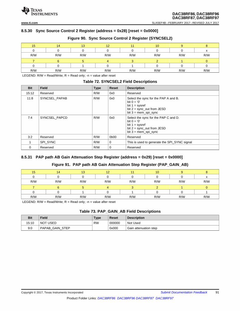
91
DAC38RF86, DAC38RF96DAC38RF87, DAC38RF97
www.ti.com SLASEF4B –FEBRUARY 2017–REVISED JULY 2017
Product Folder Links: DAC38RF86 DAC38RF96 DAC38RF87 DAC38RF97
Submit Documentation FeedbackCopyright © 2017, Texas Instruments Incorporated
8.5.30 Sync Source Control 2 Register (address = 0x28) [reset = 0x0000]
Figure 90. Sync Source Control 2 Register (SYNCSEL2)
15 14 13 12 11 10 9 80 0 0 0 0 0 0 x
R/W R/W R/W R/W R/W R/W R/W R/W
7 6 5 4 3 2 1 00 0 1 0 1 0 0 0
R/W R/W R/W R/W R/W R/W R/W R/WLEGEND: R/W = Read/Write; R = Read only; -n = value after reset
Table 72. SYNCSEL2 Field DescriptionsBit Field Type Reset Description
15:12 Reserved R/W 0x0 Reserved11:8 SYNCSEL_PAPAB R/W 0x0 Select the sync for the PAP A and B.
bit 0 = ‘0’bit 1 = sysrefbit 2 = sync_out from JESDbit 3 = mem_spi_sync
7:4 SYNCSEL_PAPCD R/W 0x0 Select the sync for the PAP C and D.bit 0 = ‘0’bit 1 = sysrefbit 2 = sync_out from JESDbit 3 = mem_spi_sync
3:2 Reserved R/W 0b00 Reserved1 SPI_SYNC R/W 0 This is used to generate the SPI_SYNC signal0 Reserved R/W 0 Reserved
8.5.31 PAP path AB Gain Attenuation Step Register (address = 0x29) [reset = 0x0000]
Figure 91. PAP path AB Gain Attenuation Step Register (PAP_GAIN_AB)
15 14 13 12 11 10 9 80 0 0 0 0 0 0 x
R/W R/W R/W R/W R/W R/W R/W R/W
7 6 5 4 3 2 1 00 0 1 0 1 0 0 1
R/W R/W R/W R/W R/W R/W R/W R/WLEGEND: R/W = Read/Write; R = Read only; -n = value after reset
Table 73. PAP_GAIN_AB Field DescriptionsBit Field Type Reset Description
15:10 NOT USED RW 000000 Not Used9:0 PAPAB_GAIN_STEP 0x000 Gain attenuation step
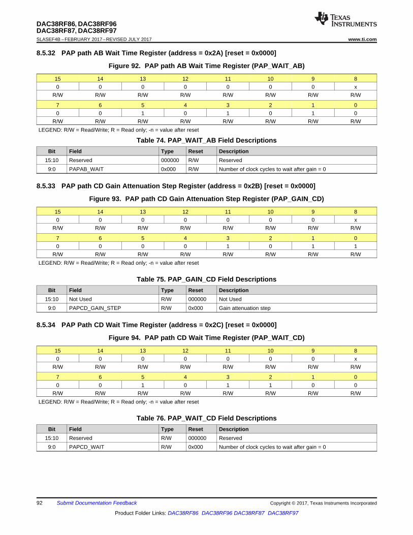
92
DAC38RF86, DAC38RF96DAC38RF87, DAC38RF97SLASEF4B –FEBRUARY 2017–REVISED JULY 2017 www.ti.com
Product Folder Links: DAC38RF86 DAC38RF96 DAC38RF87 DAC38RF97
Submit Documentation Feedback Copyright © 2017, Texas Instruments Incorporated
8.5.32 PAP path AB Wait Time Register (address = 0x2A) [reset = 0x0000]
Figure 92. PAP path AB Wait Time Register (PAP_WAIT_AB)
15 14 13 12 11 10 9 80 0 0 0 0 0 0 x
R/W R/W R/W R/W R/W R/W R/W R/W
7 6 5 4 3 2 1 00 0 1 0 1 0 1 0
R/W R/W R/W R/W R/W R/W R/W R/WLEGEND: R/W = Read/Write; R = Read only; -n = value after reset
Table 74. PAP_WAIT_AB Field DescriptionsBit Field Type Reset Description
15:10 Reserved 000000 R/W Reserved9:0 PAPAB_WAIT 0x000 R/W Number of clock cycles to wait after gain = 0
8.5.33 PAP path CD Gain Attenuation Step Register (address = 0x2B) [reset = 0x0000]
Figure 93. PAP path CD Gain Attenuation Step Register (PAP_GAIN_CD)
15 14 13 12 11 10 9 80 0 0 0 0 0 0 x
R/W R/W R/W R/W R/W R/W R/W R/W
7 6 5 4 3 2 1 00 0 0 0 1 0 1 1
R/W R/W R/W R/W R/W R/W R/W R/WLEGEND: R/W = Read/Write; R = Read only; -n = value after reset
Table 75. PAP_GAIN_CD Field DescriptionsBit Field Type Reset Description
15:10 Not Used R/W 000000 Not Used9:0 PAPCD_GAIN_STEP R/W 0x000 Gain attenuation step
8.5.34 PAP Path CD Wait Time Register (address = 0x2C) [reset = 0x0000]
Figure 94. PAP path CD Wait Time Register (PAP_WAIT_CD)
15 14 13 12 11 10 9 80 0 0 0 0 0 0 x
R/W R/W R/W R/W R/W R/W R/W R/W
7 6 5 4 3 2 1 00 0 1 0 1 1 0 0
R/W R/W R/W R/W R/W R/W R/W R/WLEGEND: R/W = Read/Write; R = Read only; -n = value after reset
Table 76. PAP_WAIT_CD Field DescriptionsBit Field Type Reset Description
15:10 Reserved R/W 000000 Reserved9:0 PAPCD_WAIT R/W 0x000 Number of clock cycles to wait after gain = 0

93
DAC38RF86, DAC38RF96DAC38RF87, DAC38RF97
www.ti.com SLASEF4B –FEBRUARY 2017–REVISED JULY 2017
Product Folder Links: DAC38RF86 DAC38RF96 DAC38RF87 DAC38RF97
Submit Documentation FeedbackCopyright © 2017, Texas Instruments Incorporated
8.5.35 PAP path AB Configuration Register (address = 0x2D) [reset = 0x0FFF]
Figure 95. PAP path AB Configuration Register (PAP_CFG_AB)
15 14 13 12 11 10 9 80 0 Reserved 0 0 0 0 x
R/W R/W R/W R/W R/W R/W R/W R/W
7 6 5 4 3 2 1 00 0 1 0 1 1 0 1
R/W R/W R/W R/W R/W R/W R/W R/WLEGEND: R/W = Read/Write; R = Read only; -n = value after reset
Table 77. PAP_CFG_AB Field DescriptionsBit Field Type Reset Description
15:14 PAPAB_SEL_DLY R/W 00
Controls the length of the delayline in the PAP AB logic.00 : N =3201 : N = 6410 : N = 12811 : Not Valid
13 Reserved R/W 0 Reserved12:0 PAPAB_THRESH R/W 0xFFF The threshold for the PAP AB trigger.
8.5.36 PAP path CD Configuration Register (address = 0x2E) [reset = 0x0FFF]
Figure 96. PAP path CD Configuration Register (PAP_CFG_CD)
15 14 13 12 11 10 9 80 0 0 0 0 0 0 x
R/W R/W R/W R/W R/W R/W R/W R/W
7 6 5 4 3 2 1 00 0 1 0 1 1 1 0
R/W R/W R/W R/W R/W R/W R/W R/WLEGEND: R/W = Read/Write; R = Read only; -n = value after reset
Table 78. PAP_CFG_CD Field DescriptionsBit Field Type Reset Description
15:14 PAPCD_SEL_DLY R/W 00
Controls the length of the delay line in the PAP CD logic.00 : N = 3201 : N = 6410 : N = 12811 : Not Valid
13 Reserved R/W 0 Reserved12:0 PAPCD_THRESH R/W 0xFFF The threshold for the PAP CD trigger.
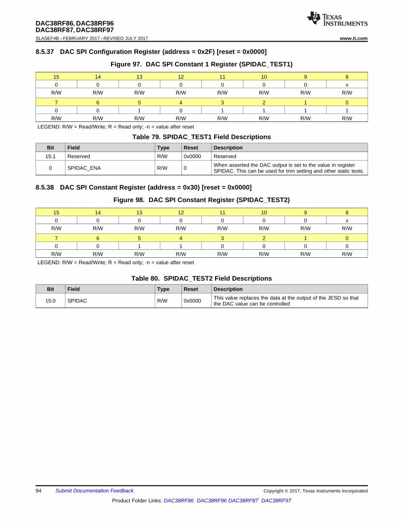
94
DAC38RF86, DAC38RF96DAC38RF87, DAC38RF97SLASEF4B –FEBRUARY 2017–REVISED JULY 2017 www.ti.com
Product Folder Links: DAC38RF86 DAC38RF96 DAC38RF87 DAC38RF97
Submit Documentation Feedback Copyright © 2017, Texas Instruments Incorporated
8.5.37 DAC SPI Configuration Register (address = 0x2F) [reset = 0x0000]
Figure 97. DAC SPI Constant 1 Register (SPIDAC_TEST1)
15 14 13 12 11 10 9 80 0 0 0 0 0 0 x
R/W R/W R/W R/W R/W R/W R/W R/W
7 6 5 4 3 2 1 00 0 1 0 1 1 1 1
R/W R/W R/W R/W R/W R/W R/W R/WLEGEND: R/W = Read/Write; R = Read only; -n = value after reset
Table 79. SPIDAC_TEST1 Field DescriptionsBit Field Type Reset Description
15:1 Reserved R/W 0x0000 Reserved
0 SPIDAC_ENA R/W 0 When asserted the DAC output is set to the value in registerSPIDAC. This can be used for trim setting and other static tests.
8.5.38 DAC SPI Constant Register (address = 0x30) [reset = 0x0000]
Figure 98. DAC SPI Constant Register (SPIDAC_TEST2)
15 14 13 12 11 10 9 80 0 0 0 0 0 0 x
R/W R/W R/W R/W R/W R/W R/W R/W
7 6 5 4 3 2 1 00 0 1 1 0 0 0 0
R/W R/W R/W R/W R/W R/W R/W R/WLEGEND: R/W = Read/Write; R = Read only; -n = value after reset
Table 80. SPIDAC_TEST2 Field DescriptionsBit Field Type Reset Description
15:0 SPIDAC R/W 0x0000 This value replaces the data at the output of the JESD so thatthe DAC value can be controlled
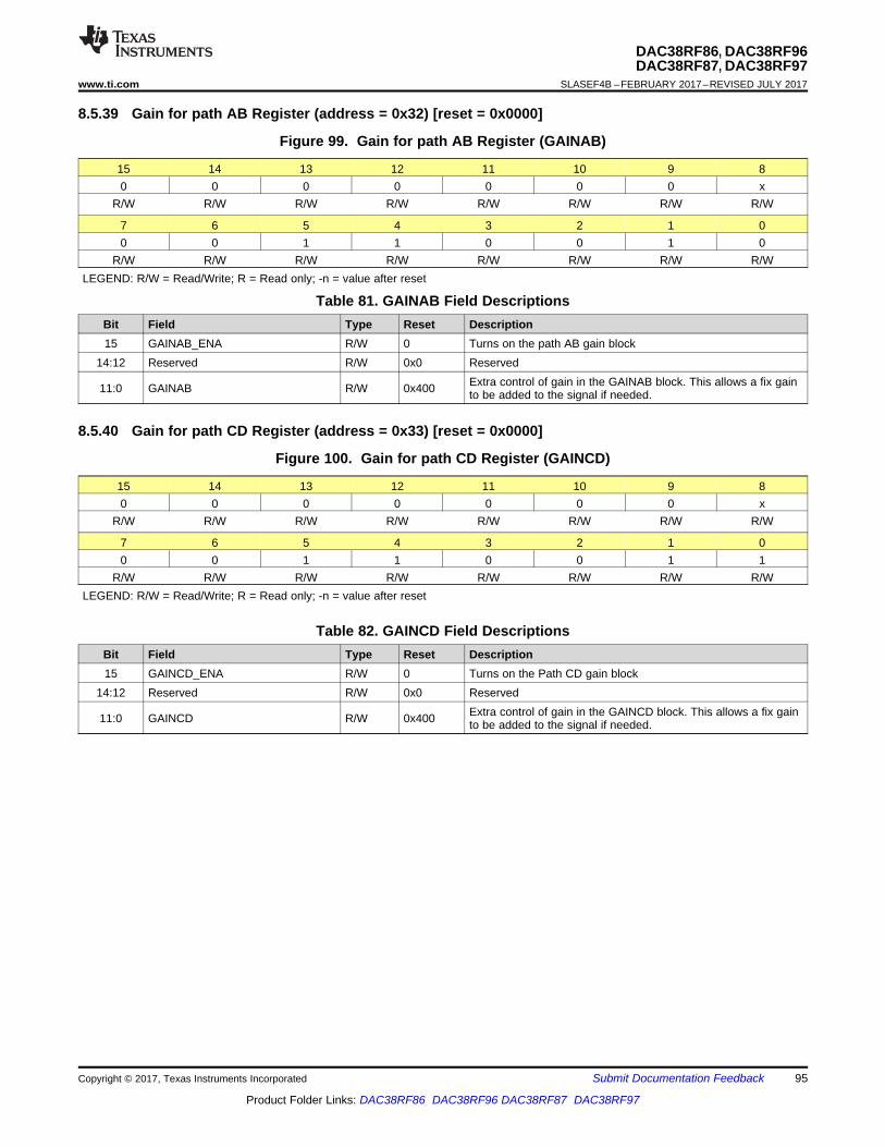
95
DAC38RF86, DAC38RF96DAC38RF87, DAC38RF97
www.ti.com SLASEF4B –FEBRUARY 2017–REVISED JULY 2017
Product Folder Links: DAC38RF86 DAC38RF96 DAC38RF87 DAC38RF97
Submit Documentation FeedbackCopyright © 2017, Texas Instruments Incorporated
8.5.39 Gain for path AB Register (address = 0x32) [reset = 0x0000]
Figure 99. Gain for path AB Register (GAINAB)
15 14 13 12 11 10 9 80 0 0 0 0 0 0 x
R/W R/W R/W R/W R/W R/W R/W R/W
7 6 5 4 3 2 1 00 0 1 1 0 0 1 0
R/W R/W R/W R/W R/W R/W R/W R/WLEGEND: R/W = Read/Write; R = Read only; -n = value after reset
Table 81. GAINAB Field DescriptionsBit Field Type Reset Description15 GAINAB_ENA R/W 0 Turns on the path AB gain block
14:12 Reserved R/W 0x0 Reserved
11:0 GAINAB R/W 0x400 Extra control of gain in the GAINAB block. This allows a fix gainto be added to the signal if needed.
8.5.40 Gain for path CD Register (address = 0x33) [reset = 0x0000]
Figure 100. Gain for path CD Register (GAINCD)
15 14 13 12 11 10 9 80 0 0 0 0 0 0 x
R/W R/W R/W R/W R/W R/W R/W R/W
7 6 5 4 3 2 1 00 0 1 1 0 0 1 1
R/W R/W R/W R/W R/W R/W R/W R/WLEGEND: R/W = Read/Write; R = Read only; -n = value after reset
Table 82. GAINCD Field DescriptionsBit Field Type Reset Description15 GAINCD_ENA R/W 0 Turns on the Path CD gain block
14:12 Reserved R/W 0x0 Reserved
11:0 GAINCD R/W 0x400 Extra control of gain in the GAINCD block. This allows a fix gainto be added to the signal if needed.
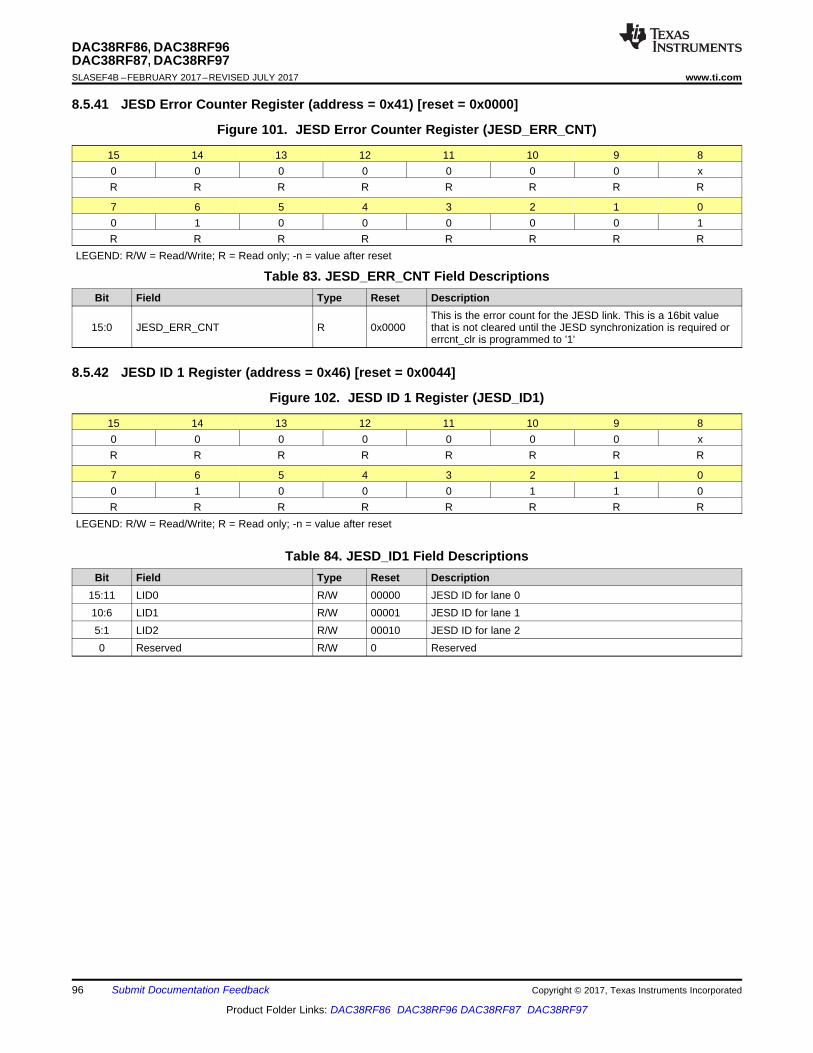
96
DAC38RF86, DAC38RF96DAC38RF87, DAC38RF97SLASEF4B –FEBRUARY 2017–REVISED JULY 2017 www.ti.com
Product Folder Links: DAC38RF86 DAC38RF96 DAC38RF87 DAC38RF97
Submit Documentation Feedback Copyright © 2017, Texas Instruments Incorporated
8.5.41 JESD Error Counter Register (address = 0x41) [reset = 0x0000]
Figure 101. JESD Error Counter Register (JESD_ERR_CNT)
15 14 13 12 11 10 9 80 0 0 0 0 0 0 xR R R R R R R R
7 6 5 4 3 2 1 00 1 0 0 0 0 0 1R R R R R R R R
LEGEND: R/W = Read/Write; R = Read only; -n = value after reset
Table 83. JESD_ERR_CNT Field DescriptionsBit Field Type Reset Description
15:0 JESD_ERR_CNT R 0x0000This is the error count for the JESD link. This is a 16bit valuethat is not cleared until the JESD synchronization is required orerrcnt_clr is programmed to '1'
8.5.42 JESD ID 1 Register (address = 0x46) [reset = 0x0044]
Figure 102. JESD ID 1 Register (JESD_ID1)
15 14 13 12 11 10 9 80 0 0 0 0 0 0 xR R R R R R R R
7 6 5 4 3 2 1 00 1 0 0 0 1 1 0R R R R R R R R
LEGEND: R/W = Read/Write; R = Read only; -n = value after reset
Table 84. JESD_ID1 Field DescriptionsBit Field Type Reset Description
15:11 LID0 R/W 00000 JESD ID for lane 010:6 LID1 R/W 00001 JESD ID for lane 15:1 LID2 R/W 00010 JESD ID for lane 20 Reserved R/W 0 Reserved
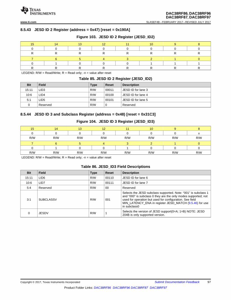
97
DAC38RF86, DAC38RF96DAC38RF87, DAC38RF97
www.ti.com SLASEF4B –FEBRUARY 2017–REVISED JULY 2017
Product Folder Links: DAC38RF86 DAC38RF96 DAC38RF87 DAC38RF97
Submit Documentation FeedbackCopyright © 2017, Texas Instruments Incorporated
8.5.43 JESD ID 2 Register (address = 0x47) [reset = 0x190A]
Figure 103. JESD ID 2 Register (JESD_ID2)
15 14 13 12 11 10 9 80 0 0 0 0 0 0 0R R R R R R R R
7 6 5 4 3 2 1 00 1 0 0 0 1 1 1R R R R R R R R
LEGEND: R/W = Read/Write; R = Read only; -n = value after reset
Table 85. JESD ID 2 Register (JESD_ID2)Bit Field Type Reset Description
15:11 LID3 R/W 00011 JESD ID for lane 310:6 LID4 R/W 00100 JESD ID for lane 45:1 LID5 R/W 00101 JESD ID for lane 50 Reserved R/W 0 Reserved
8.5.44 JESD ID 3 and Subclass Register (address = 0x48) [reset = 0x31C3]
Figure 104. JESD ID 3 Register (JESD_ID3)
15 14 13 12 11 10 9 80 0 0 0 0 0 0 x
R/W R/W R/W R/W R/W R/W R/W R/W
7 6 5 4 3 2 1 00 1 0 0 1 0 0 0
R/W R/W R/W R/W R/W R/W R/W R/WLEGEND: R/W = Read/Write; R = Read only; -n = value after reset
Table 86. JESD_ID3 Field DescriptionsBit Field Type Reset Description
15:11 LID6 R/W 00110 JESD ID for lane 610:6 LID7 R/W 00111 JESD ID for lane 75:4 Reserved R/W 00 Reserved
3:1 SUBCLASSV R/W 001
Selects the JESD subclass supported. Note: “001” is subclass 1and “000” is subclass 0 they are the only modes supported; notused for operation but used for configuration. See fieldMIN_LATENCY_ENA in register JESD_MATCH (9.5.46) for usein subclass0
0 JESDV R/W 1 Selects the version of JESD support(0=A; 1=B) NOTE: JESD204B is only supported version.
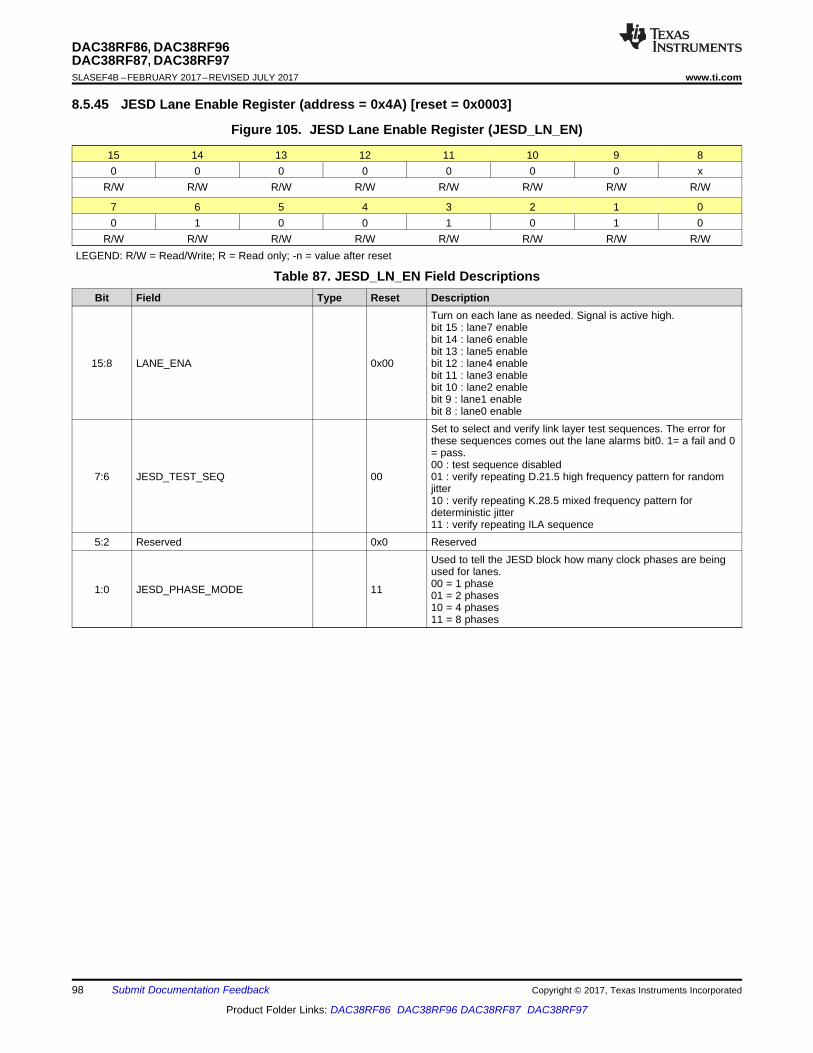
98
DAC38RF86, DAC38RF96DAC38RF87, DAC38RF97SLASEF4B –FEBRUARY 2017–REVISED JULY 2017 www.ti.com
Product Folder Links: DAC38RF86 DAC38RF96 DAC38RF87 DAC38RF97
Submit Documentation Feedback Copyright © 2017, Texas Instruments Incorporated
8.5.45 JESD Lane Enable Register (address = 0x4A) [reset = 0x0003]
Figure 105. JESD Lane Enable Register (JESD_LN_EN)
15 14 13 12 11 10 9 80 0 0 0 0 0 0 x
R/W R/W R/W R/W R/W R/W R/W R/W
7 6 5 4 3 2 1 00 1 0 0 1 0 1 0
R/W R/W R/W R/W R/W R/W R/W R/WLEGEND: R/W = Read/Write; R = Read only; -n = value after reset
Table 87. JESD_LN_EN Field DescriptionsBit Field Type Reset Description
15:8 LANE_ENA 0x00
Turn on each lane as needed. Signal is active high.bit 15 : lane7 enablebit 14 : lane6 enablebit 13 : lane5 enablebit 12 : lane4 enablebit 11 : lane3 enablebit 10 : lane2 enablebit 9 : lane1 enablebit 8 : lane0 enable
7:6 JESD_TEST_SEQ 00
Set to select and verify link layer test sequences. The error forthese sequences comes out the lane alarms bit0. 1= a fail and 0= pass.00 : test sequence disabled01 : verify repeating D.21.5 high frequency pattern for randomjitter10 : verify repeating K.28.5 mixed frequency pattern fordeterministic jitter11 : verify repeating ILA sequence
5:2 Reserved 0x0 Reserved
1:0 JESD_PHASE_MODE 11
Used to tell the JESD block how many clock phases are beingused for lanes.00 = 1 phase01 = 2 phases10 = 4 phases11 = 8 phases
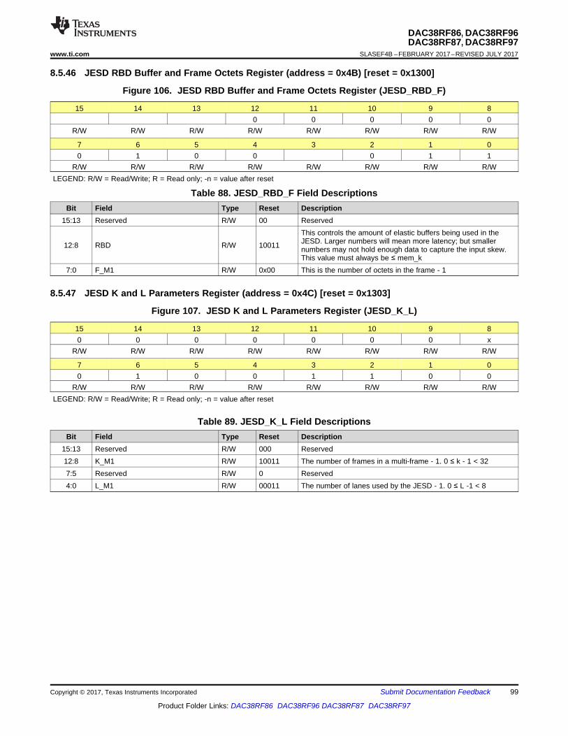
99
DAC38RF86, DAC38RF96DAC38RF87, DAC38RF97
www.ti.com SLASEF4B –FEBRUARY 2017–REVISED JULY 2017
Product Folder Links: DAC38RF86 DAC38RF96 DAC38RF87 DAC38RF97
Submit Documentation FeedbackCopyright © 2017, Texas Instruments Incorporated
8.5.46 JESD RBD Buffer and Frame Octets Register (address = 0x4B) [reset = 0x1300]
Figure 106. JESD RBD Buffer and Frame Octets Register (JESD_RBD_F)
15 14 13 12 11 10 9 80 0 0 0 0
R/W R/W R/W R/W R/W R/W R/W R/W
7 6 5 4 3 2 1 00 1 0 0 0 1 1
R/W R/W R/W R/W R/W R/W R/W R/WLEGEND: R/W = Read/Write; R = Read only; -n = value after reset
Table 88. JESD_RBD_F Field DescriptionsBit Field Type Reset Description
15:13 Reserved R/W 00 Reserved
12:8 RBD R/W 10011
This controls the amount of elastic buffers being used in theJESD. Larger numbers will mean more latency; but smallernumbers may not hold enough data to capture the input skew.This value must always be ≤ mem_k
7:0 F_M1 R/W 0x00 This is the number of octets in the frame - 1
8.5.47 JESD K and L Parameters Register (address = 0x4C) [reset = 0x1303]
Figure 107. JESD K and L Parameters Register (JESD_K_L)
15 14 13 12 11 10 9 80 0 0 0 0 0 0 x
R/W R/W R/W R/W R/W R/W R/W R/W
7 6 5 4 3 2 1 00 1 0 0 1 1 0 0
R/W R/W R/W R/W R/W R/W R/W R/WLEGEND: R/W = Read/Write; R = Read only; -n = value after reset
Table 89. JESD_K_L Field DescriptionsBit Field Type Reset Description
15:13 Reserved R/W 000 Reserved12:8 K_M1 R/W 10011 The number of frames in a multi-frame - 1. 0 ≤ k - 1 < 327:5 Reserved R/W 0 Reserved4:0 L_M1 R/W 00011 The number of lanes used by the JESD - 1. 0 ≤ L -1 < 8
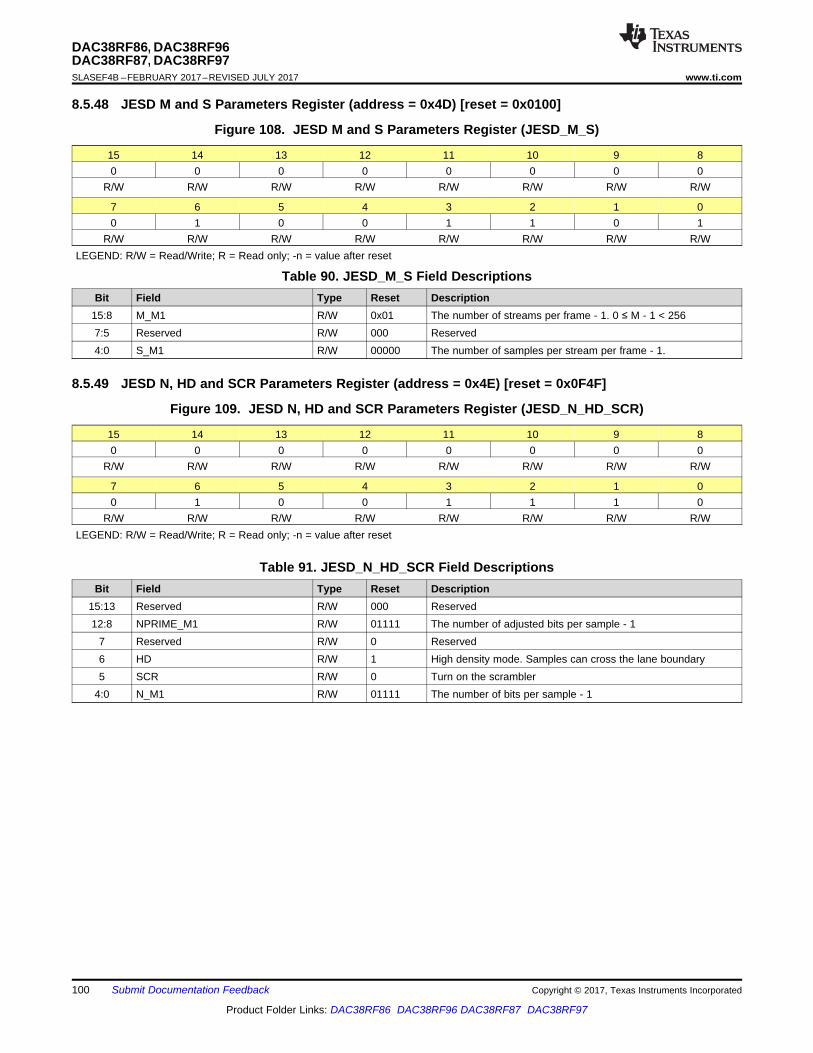
100
DAC38RF86, DAC38RF96DAC38RF87, DAC38RF97SLASEF4B –FEBRUARY 2017–REVISED JULY 2017 www.ti.com
Product Folder Links: DAC38RF86 DAC38RF96 DAC38RF87 DAC38RF97
Submit Documentation Feedback Copyright © 2017, Texas Instruments Incorporated
8.5.48 JESD M and S Parameters Register (address = 0x4D) [reset = 0x0100]
Figure 108. JESD M and S Parameters Register (JESD_M_S)
15 14 13 12 11 10 9 80 0 0 0 0 0 0 0
R/W R/W R/W R/W R/W R/W R/W R/W
7 6 5 4 3 2 1 00 1 0 0 1 1 0 1
R/W R/W R/W R/W R/W R/W R/W R/WLEGEND: R/W = Read/Write; R = Read only; -n = value after reset
Table 90. JESD_M_S Field DescriptionsBit Field Type Reset Description
15:8 M_M1 R/W 0x01 The number of streams per frame - 1. 0 ≤ M - 1 < 2567:5 Reserved R/W 000 Reserved4:0 S_M1 R/W 00000 The number of samples per stream per frame - 1.
8.5.49 JESD N, HD and SCR Parameters Register (address = 0x4E) [reset = 0x0F4F]
Figure 109. JESD N, HD and SCR Parameters Register (JESD_N_HD_SCR)
15 14 13 12 11 10 9 80 0 0 0 0 0 0 0
R/W R/W R/W R/W R/W R/W R/W R/W
7 6 5 4 3 2 1 00 1 0 0 1 1 1 0
R/W R/W R/W R/W R/W R/W R/W R/WLEGEND: R/W = Read/Write; R = Read only; -n = value after reset
Table 91. JESD_N_HD_SCR Field DescriptionsBit Field Type Reset Description
15:13 Reserved R/W 000 Reserved12:8 NPRIME_M1 R/W 01111 The number of adjusted bits per sample - 1
7 Reserved R/W 0 Reserved6 HD R/W 1 High density mode. Samples can cross the lane boundary5 SCR R/W 0 Turn on the scrambler
4:0 N_M1 R/W 01111 The number of bits per sample - 1
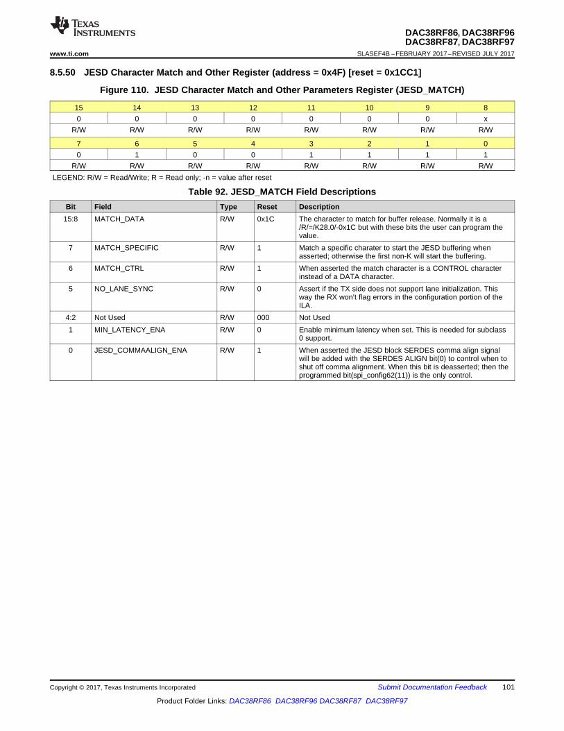
101
DAC38RF86, DAC38RF96DAC38RF87, DAC38RF97
www.ti.com SLASEF4B –FEBRUARY 2017–REVISED JULY 2017
Product Folder Links: DAC38RF86 DAC38RF96 DAC38RF87 DAC38RF97
Submit Documentation FeedbackCopyright © 2017, Texas Instruments Incorporated
8.5.50 JESD Character Match and Other Register (address = 0x4F) [reset = 0x1CC1]
Figure 110. JESD Character Match and Other Parameters Register (JESD_MATCH)
15 14 13 12 11 10 9 80 0 0 0 0 0 0 x
R/W R/W R/W R/W R/W R/W R/W R/W
7 6 5 4 3 2 1 00 1 0 0 1 1 1 1
R/W R/W R/W R/W R/W R/W R/W R/WLEGEND: R/W = Read/Write; R = Read only; -n = value after reset
Table 92. JESD_MATCH Field DescriptionsBit Field Type Reset Description
15:8 MATCH_DATA R/W 0x1C The character to match for buffer release. Normally it is a/R/=/K28.0/-0x1C but with these bits the user can program thevalue.
7 MATCH_SPECIFIC R/W 1 Match a specific charater to start the JESD buffering whenasserted; otherwise the first non-K will start the buffering.
6 MATCH_CTRL R/W 1 When asserted the match character is a CONTROL characterinstead of a DATA character.
5 NO_LANE_SYNC R/W 0 Assert if the TX side does not support lane initialization. Thisway the RX won’t flag errors in the configuration portion of theILA.
4:2 Not Used R/W 000 Not Used1 MIN_LATENCY_ENA R/W 0 Enable minimum latency when set. This is needed for subclass
0 support.0 JESD_COMMAALIGN_ENA R/W 1 When asserted the JESD block SERDES comma align signal
will be added with the SERDES ALIGN bit(0) to control when toshut off comma alignment. When this bit is deasserted; then theprogrammed bit(spi_config62(11)) is the only control.
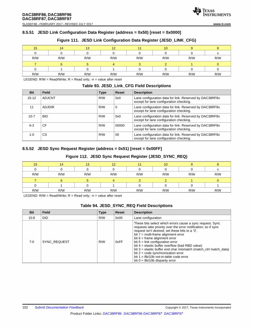
102
DAC38RF86, DAC38RF96DAC38RF87, DAC38RF97SLASEF4B –FEBRUARY 2017–REVISED JULY 2017 www.ti.com
Product Folder Links: DAC38RF86 DAC38RF96 DAC38RF87 DAC38RF97
Submit Documentation Feedback Copyright © 2017, Texas Instruments Incorporated
8.5.51 JESD Link Configuration Data Register (address = 0x50) [reset = 0x0000]
Figure 111. JESD Link Configuration Data Register (JESD_LINK_CFG)
15 14 13 12 11 10 9 80 0 0 0 0 0 0 x
R/W R/W R/W R/W R/W R/W R/W R/W
7 6 5 4 3 2 1 00 1 0 1 0 0 0 0
R/W R/W R/W R/W R/W R/W R/W R/WLEGEND: R/W = Read/Write; R = Read only; -n = value after reset
Table 93. JESD_Link_CFG Field DescriptionsBit Field Type Reset Description
15-12 ADJCNT R/W 0x0 Lane configuration data for link. Reserved by DAC38RF8xexcept for lane configuration checking.
11 ADJDIR R/W 0 Lane configuration data for link. Reserved by DAC38RF8xexcept for lane configuration checking.
10-7 BID R/W 0x0 Lane configuration data for link. Reserved by DAC38RF8xexcept for lane configuration checking.
6-2 CF R/W 00000 Lane configuration data for link. Reserved by DAC38RF8xexcept for lane configuration checking.
1-0 CS R/W 00 Lane configuration data for link. Reserved by DAC38RF8xexcept for lane configuration checking.
8.5.52 JESD Sync Request Register (address = 0x51) [reset = 0x00FF]
Figure 112. JESD Sync Request Register (JESD_SYNC_REQ)
15 14 13 12 11 10 9 80 0 0 0 0 0 0 x
R/W R/W R/W R/W R/W R/W R/W R/W
7 6 5 4 3 2 1 00 1 0 1 0 0 0 1
R/W R/W R/W R/W R/W R/W R/W R/WLEGEND: R/W = Read/Write; R = Read only; -n = value after reset
Table 94. JESD_SYNC_REQ Field DescriptionsBit Field Type Reset Description
15:8 DID R/W 0x00 Lane configuration
7:0 SYNC_REQUEST R/W 0xFF
These bits select which errors cause a sync request. Syncrequests take priority over the error notification; so if syncrequest isn’t desired; set these bits to a ‘0’.bit 7 = multi-frame alignment errorbit 6 = frame alignment errorbit 5 = link configuration errorbit 4 = elastic buffer overflow (bad RBD value)bit 3 = elastic buffer end char mismatch (match_ctrl match_data)bit 2 = code synchronization errorbit 1 = 8b/10b not-in-table code errorbit 0 = 8b/10b disparity error

103
DAC38RF86, DAC38RF96DAC38RF87, DAC38RF97
www.ti.com SLASEF4B –FEBRUARY 2017–REVISED JULY 2017
Product Folder Links: DAC38RF86 DAC38RF96 DAC38RF87 DAC38RF97
Submit Documentation FeedbackCopyright © 2017, Texas Instruments Incorporated
8.5.53 JESD Error Output Register (address = 0x52) [reset = 0x00FF]
Figure 113. JESD Error Output Register (JESD_ERR_OUT)
15 14 13 12 11 10 9 80 0 0 0 0 0 0 x
R/W R/W R/W R/W R/W R/W R/W R/W
7 6 5 4 3 2 1 00 1 0 1 0 0 1 0
R/W R/W R/W R/W R/W R/W R/W R/WLEGEND: R/W = Read/Write; R = Read only; -n = value after reset
Table 95. JESD_ERR_OUT Field DescriptionsBit Field Type Reset Description
15:10 Reserved R/W 000000 Reserved
9 DISABLE_ERR_RPT R/W 0 Assertion means that errors will not be reported on the sync_noutput.
8 PHADJ R/W 0 Lane configuration
7:0 ERR_ENA R/W 0xFF
These bits select the errors generated are counted in the err_cfor the link. The bits also control what signals are sent out thepad_syncb pin for error notification.bit 7 = multi-frame alignment errorbit 6 = frame alignment errorbit 5 = link configuration errorbit 4 = elastic buffer overflow (bad RBD value)bit 3 = elastic buffer end char mismatch (match_ctrl match_data)bit 2 = code synchronization errorbit 1 = 8b/10b not-in-table code errorbit 0 = 8b/10b disparity error
8.5.54 JESD ILA Check 1 Register (address = 0x53) [reset = 0x0100]
Figure 114. JESD ILA Check 1 Register (JESD_ILA_CFG1)
15 14 13 12 11 10 9 80 0 0 0 0 0 0 x
R/W R/W R/W R/W R/W R/W R/W R/W
7 6 5 4 3 2 1 00 1 0 1 0 0 1 1
R/W R/W R/W R/W R/W R/W R/W R/WLEGEND: R/W = Read/Write; R = Read only; -n = value after reset
Table 96. JESD_ILA_CFG1 Field DescriptionsBit Field Type Reset Description
15:8 ILA_M R/W 0x01 JESD M-1 configuration value used only for ILA checking; maybe set independently of the actual JESD mode
7:0 ILA_F R/W 0x00 JESD F-1 configuration value used only for ILA checking; maybe set independently of the actual JESD mode
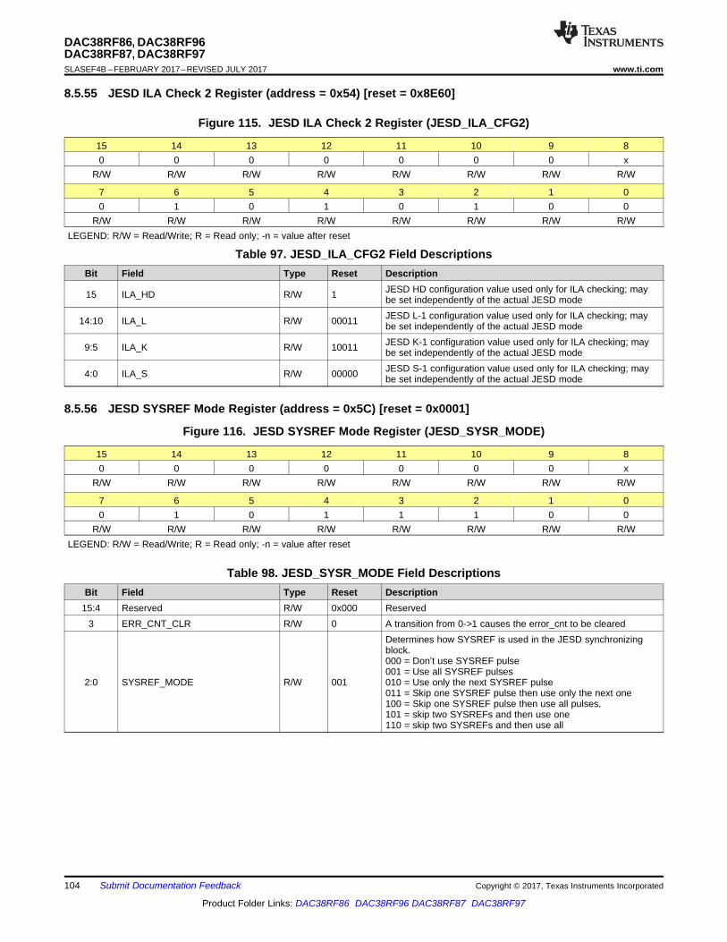
104
DAC38RF86, DAC38RF96DAC38RF87, DAC38RF97SLASEF4B –FEBRUARY 2017–REVISED JULY 2017 www.ti.com
Product Folder Links: DAC38RF86 DAC38RF96 DAC38RF87 DAC38RF97
Submit Documentation Feedback Copyright © 2017, Texas Instruments Incorporated
8.5.55 JESD ILA Check 2 Register (address = 0x54) [reset = 0x8E60]
Figure 115. JESD ILA Check 2 Register (JESD_ILA_CFG2)
15 14 13 12 11 10 9 80 0 0 0 0 0 0 x
R/W R/W R/W R/W R/W R/W R/W R/W
7 6 5 4 3 2 1 00 1 0 1 0 1 0 0
R/W R/W R/W R/W R/W R/W R/W R/WLEGEND: R/W = Read/Write; R = Read only; -n = value after reset
Table 97. JESD_ILA_CFG2 Field DescriptionsBit Field Type Reset Description
15 ILA_HD R/W 1 JESD HD configuration value used only for ILA checking; maybe set independently of the actual JESD mode
14:10 ILA_L R/W 00011 JESD L-1 configuration value used only for ILA checking; maybe set independently of the actual JESD mode
9:5 ILA_K R/W 10011 JESD K-1 configuration value used only for ILA checking; maybe set independently of the actual JESD mode
4:0 ILA_S R/W 00000 JESD S-1 configuration value used only for ILA checking; maybe set independently of the actual JESD mode
8.5.56 JESD SYSREF Mode Register (address = 0x5C) [reset = 0x0001]
Figure 116. JESD SYSREF Mode Register (JESD_SYSR_MODE)
15 14 13 12 11 10 9 80 0 0 0 0 0 0 x
R/W R/W R/W R/W R/W R/W R/W R/W
7 6 5 4 3 2 1 00 1 0 1 1 1 0 0
R/W R/W R/W R/W R/W R/W R/W R/WLEGEND: R/W = Read/Write; R = Read only; -n = value after reset
Table 98. JESD_SYSR_MODE Field DescriptionsBit Field Type Reset Description
15:4 Reserved R/W 0x000 Reserved3 ERR_CNT_CLR R/W 0 A transition from 0->1 causes the error_cnt to be cleared
2:0 SYSREF_MODE R/W 001
Determines how SYSREF is used in the JESD synchronizingblock.000 = Don’t use SYSREF pulse001 = Use all SYSREF pulses010 = Use only the next SYSREF pulse011 = Skip one SYSREF pulse then use only the next one100 = Skip one SYSREF pulse then use all pulses.101 = skip two SYSREFs and then use one110 = skip two SYSREFs and then use all
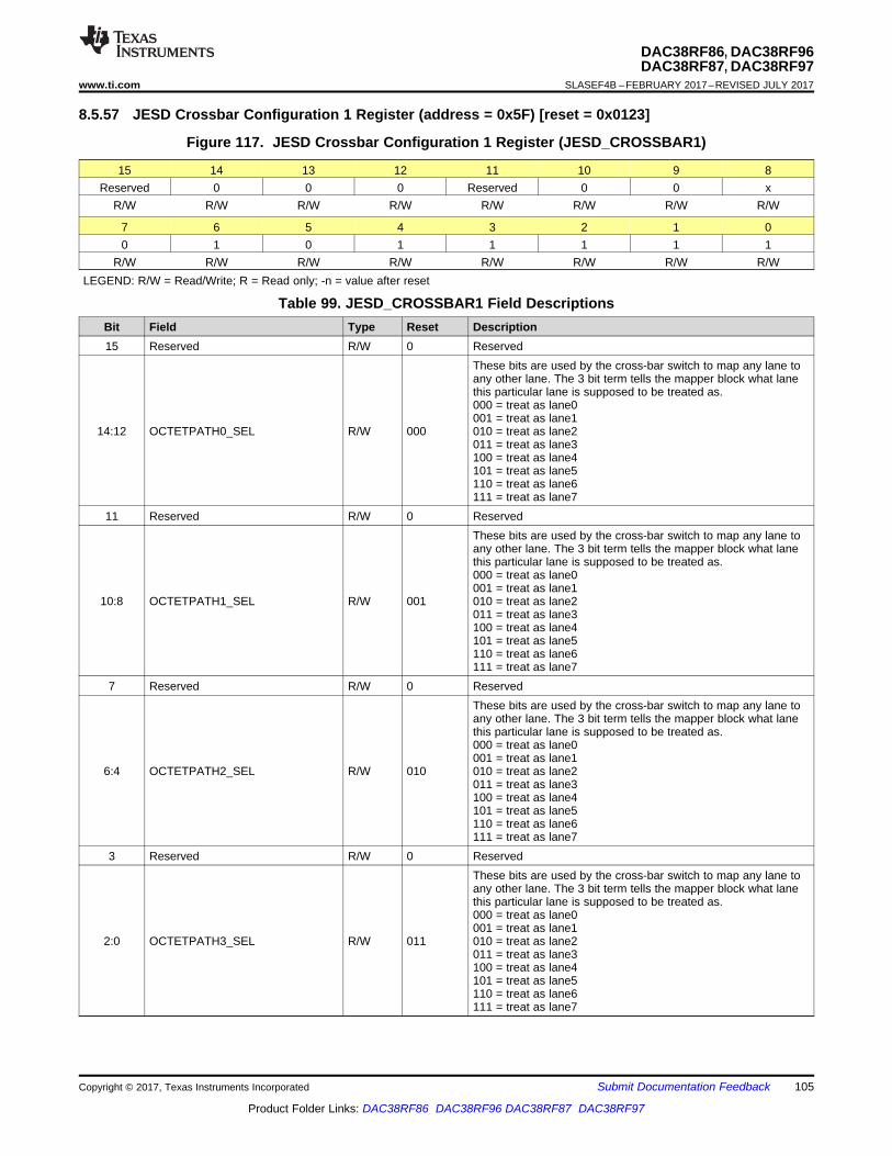
105
DAC38RF86, DAC38RF96DAC38RF87, DAC38RF97
www.ti.com SLASEF4B –FEBRUARY 2017–REVISED JULY 2017
Product Folder Links: DAC38RF86 DAC38RF96 DAC38RF87 DAC38RF97
Submit Documentation FeedbackCopyright © 2017, Texas Instruments Incorporated
8.5.57 JESD Crossbar Configuration 1 Register (address = 0x5F) [reset = 0x0123]
Figure 117. JESD Crossbar Configuration 1 Register (JESD_CROSSBAR1)
15 14 13 12 11 10 9 8Reserved 0 0 0 Reserved 0 0 x
R/W R/W R/W R/W R/W R/W R/W R/W
7 6 5 4 3 2 1 00 1 0 1 1 1 1 1
R/W R/W R/W R/W R/W R/W R/W R/WLEGEND: R/W = Read/Write; R = Read only; -n = value after reset
Table 99. JESD_CROSSBAR1 Field DescriptionsBit Field Type Reset Description15 Reserved R/W 0 Reserved
14:12 OCTETPATH0_SEL R/W 000
These bits are used by the cross-bar switch to map any lane toany other lane. The 3 bit term tells the mapper block what lanethis particular lane is supposed to be treated as.000 = treat as lane0001 = treat as lane1010 = treat as lane2011 = treat as lane3100 = treat as lane4101 = treat as lane5110 = treat as lane6111 = treat as lane7
11 Reserved R/W 0 Reserved
10:8 OCTETPATH1_SEL R/W 001
These bits are used by the cross-bar switch to map any lane toany other lane. The 3 bit term tells the mapper block what lanethis particular lane is supposed to be treated as.000 = treat as lane0001 = treat as lane1010 = treat as lane2011 = treat as lane3100 = treat as lane4101 = treat as lane5110 = treat as lane6111 = treat as lane7
7 Reserved R/W 0 Reserved
6:4 OCTETPATH2_SEL R/W 010
These bits are used by the cross-bar switch to map any lane toany other lane. The 3 bit term tells the mapper block what lanethis particular lane is supposed to be treated as.000 = treat as lane0001 = treat as lane1010 = treat as lane2011 = treat as lane3100 = treat as lane4101 = treat as lane5110 = treat as lane6111 = treat as lane7
3 Reserved R/W 0 Reserved
2:0 OCTETPATH3_SEL R/W 011
These bits are used by the cross-bar switch to map any lane toany other lane. The 3 bit term tells the mapper block what lanethis particular lane is supposed to be treated as.000 = treat as lane0001 = treat as lane1010 = treat as lane2011 = treat as lane3100 = treat as lane4101 = treat as lane5110 = treat as lane6111 = treat as lane7

106
DAC38RF86, DAC38RF96DAC38RF87, DAC38RF97SLASEF4B –FEBRUARY 2017–REVISED JULY 2017 www.ti.com
Product Folder Links: DAC38RF86 DAC38RF96 DAC38RF87 DAC38RF97
Submit Documentation Feedback Copyright © 2017, Texas Instruments Incorporated
8.5.58 JESD Crossbar Configuration 2 Register (address = 0x60) [reset = 0x4567]
Figure 118. JESD_CROSSBAR2 Field DBits to Determine What Version of Build for the chip.escriptions
15 14 13 12 11 10 9 80 0 0 0 0 0 0 x
R/W R/W R/W R/W R/W R/W R/W R/W
7 6 5 4 3 2 1 00 1 1 0 0 0 0 1
R/W R/W R/W R/W R/W R/W R/W R/WLEGEND: R/W = Read/Write; R = Read only; -n = value after reset
Table 100. JESD_CROSSBAR2 Field DescriptionsBit Field Type Reset Description15 Reserved R/W 0 Reserved
14:12 OCTETPATH4_SEL R/W 100
These bits are used by the cross-bar switch to map any lane toany other lane. The 3 bit term tells the mapper block what lanethis particular lane is supposed to be treated as.000 = treat as lane0001 = treat as lane1010 = treat as lane2011 = treat as lane3100 = treat as lane4101 = treat as lane5110 = treat as lane6111 = treat as lane7
11 Reserved R/W 0 Reserved
10:8 OCTETPATH5_SEL R/W 101
These bits are used by the cross-bar switch to map any lane toany other lane. The 3 bit term tells the mapper block what lanethis particular lane is supposed to be treated as.000 = treat as lane0001 = treat as lane1010 = treat as lane2011 = treat as lane3100 = treat as lane4101 = treat as lane5110 = treat as lane6111 = treat as lane7
7 Reserved R/W 0 Reserved
6:4 OCTETPATH6_SEL R/W 110
These bits are used by the cross-bar switch to map any lane toany other lane. The 3 bit term tells the mapper block what lanethis particular lane is supposed to be treated as.000 = treat as lane0001 = treat as lane1010 = treat as lane2011 = treat as lane3100 = treat as lane4101 = treat as lane5110 = treat as lane6111 = treat as lane7
3 Reserved R/W 0 Reserved
2:0 OCTETPATH7_SEL R/W 111
These bits are used by the cross-bar switch to map any lane toany other lane. The 3 bit term tells the mapper block what lanethis particular lane is supposed to be treated as.000 = treat as lane0001 = treat as lane1010 = treat as lane2011 = treat as lane3100 = treat as lane4101 = treat as lane5110 = treat as lane6111 = treat as lane7

107
DAC38RF86, DAC38RF96DAC38RF87, DAC38RF97
www.ti.com SLASEF4B –FEBRUARY 2017–REVISED JULY 2017
Product Folder Links: DAC38RF86 DAC38RF96 DAC38RF87 DAC38RF97
Submit Documentation FeedbackCopyright © 2017, Texas Instruments Incorporated
8.5.59 JESD Alarms for Lane 0 Register (address = 0x64) [reset = 0x0000]
Figure 119. JESD Alarms for Lane 0 Register (JBits to determine what version of build for thechip.ESD_ALM_L0)
15 14 13 12 11 10 9 80 0 0 0 0 0 0 x
W0C W0C W0C W0C W0C W0C W0C W0C
7 6 5 4 3 2 1 00 1 1 0 0 1 0 0
W0C W0C W0C W0C W0C W0C W0C W0CLEGEND: R/W = Read/Write; R = Read only; W0C = Write 0 to clear bit; -n = value after reset; -n = value after reset
Table 101. JESD_ALM_L0 Field DescriptionsBit Field Type Reset Description
15:8 ALM_LANE0_ERR W0C 0x00
Lane0 errors:bit 15 = multiframe alignment errorbit 14 = frame alignment errorbit 13 = link configuration errorbit 12 = elastic buffer overflow (bad RBD value)bit 11 = elastic buffer match error. The first non-/K/ doesn’tmatch “match_ctrl” and “match_data” programmed values.bit 10 = code synchronization errorbit 9 = 8b/10b not-in-table code errorbit 8 = 8b/10b disparity error
7:4 Reserved W0C 0x0 Reserved
3:0 ALM_FIFO0_FLAGS W0C 0x0
Lane0 FIFO errors:bit 3 = write_error : High if write request and FIFO is full (NOTE:only released when JESD block is initialize with mem_init_state)bit 2 = write_full : FIFO is FULLbit 1 = read_error : High if read request with empty FIFO (NOTE:only released when JESD block is initialize with mem_init_state)bit 0 = read_empty : FIFO is empty
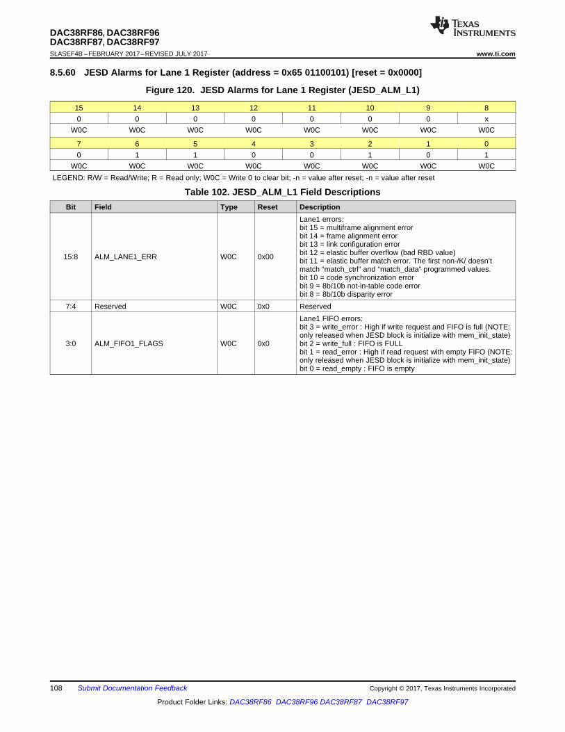
108
DAC38RF86, DAC38RF96DAC38RF87, DAC38RF97SLASEF4B –FEBRUARY 2017–REVISED JULY 2017 www.ti.com
Product Folder Links: DAC38RF86 DAC38RF96 DAC38RF87 DAC38RF97
Submit Documentation Feedback Copyright © 2017, Texas Instruments Incorporated
8.5.60 JESD Alarms for Lane 1 Register (address = 0x65 01100101) [reset = 0x0000]
Figure 120. JESD Alarms for Lane 1 Register (JESD_ALM_L1)
15 14 13 12 11 10 9 80 0 0 0 0 0 0 x
W0C W0C W0C W0C W0C W0C W0C W0C
7 6 5 4 3 2 1 00 1 1 0 0 1 0 1
W0C W0C W0C W0C W0C W0C W0C W0CLEGEND: R/W = Read/Write; R = Read only; W0C = Write 0 to clear bit; -n = value after reset; -n = value after reset
Table 102. JESD_ALM_L1 Field DescriptionsBit Field Type Reset Description
15:8 ALM_LANE1_ERR W0C 0x00
Lane1 errors:bit 15 = multiframe alignment errorbit 14 = frame alignment errorbit 13 = link configuration errorbit 12 = elastic buffer overflow (bad RBD value)bit 11 = elastic buffer match error. The first non-/K/ doesn’tmatch “match_ctrl” and “match_data” programmed values.bit 10 = code synchronization errorbit 9 = 8b/10b not-in-table code errorbit 8 = 8b/10b disparity error
7:4 Reserved W0C 0x0 Reserved
3:0 ALM_FIFO1_FLAGS W0C 0x0
Lane1 FIFO errors:bit 3 = write_error : High if write request and FIFO is full (NOTE:only released when JESD block is initialize with mem_init_state)bit 2 = write_full : FIFO is FULLbit 1 = read_error : High if read request with empty FIFO (NOTE:only released when JESD block is initialize with mem_init_state)bit 0 = read_empty : FIFO is empty
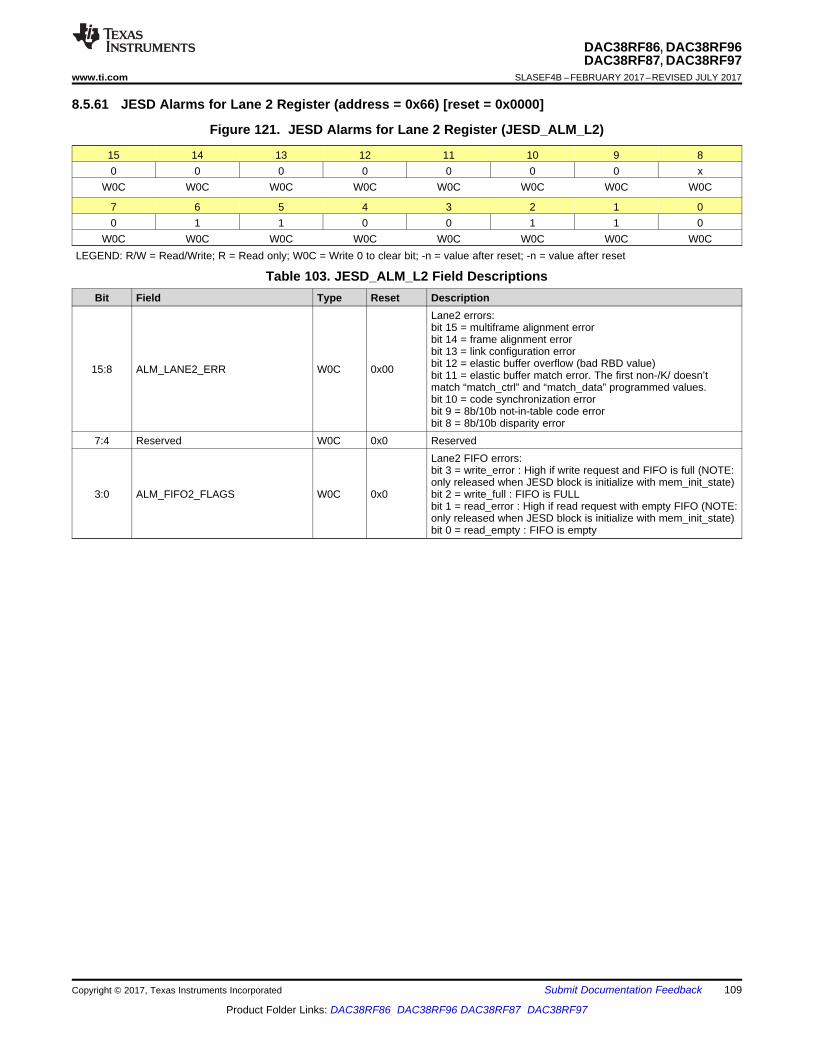
109
DAC38RF86, DAC38RF96DAC38RF87, DAC38RF97
www.ti.com SLASEF4B –FEBRUARY 2017–REVISED JULY 2017
Product Folder Links: DAC38RF86 DAC38RF96 DAC38RF87 DAC38RF97
Submit Documentation FeedbackCopyright © 2017, Texas Instruments Incorporated
8.5.61 JESD Alarms for Lane 2 Register (address = 0x66) [reset = 0x0000]
Figure 121. JESD Alarms for Lane 2 Register (JESD_ALM_L2)
15 14 13 12 11 10 9 80 0 0 0 0 0 0 x
W0C W0C W0C W0C W0C W0C W0C W0C
7 6 5 4 3 2 1 00 1 1 0 0 1 1 0
W0C W0C W0C W0C W0C W0C W0C W0CLEGEND: R/W = Read/Write; R = Read only; W0C = Write 0 to clear bit; -n = value after reset; -n = value after reset
Table 103. JESD_ALM_L2 Field DescriptionsBit Field Type Reset Description
15:8 ALM_LANE2_ERR W0C 0x00
Lane2 errors:bit 15 = multiframe alignment errorbit 14 = frame alignment errorbit 13 = link configuration errorbit 12 = elastic buffer overflow (bad RBD value)bit 11 = elastic buffer match error. The first non-/K/ doesn’tmatch “match_ctrl” and “match_data” programmed values.bit 10 = code synchronization errorbit 9 = 8b/10b not-in-table code errorbit 8 = 8b/10b disparity error
7:4 Reserved W0C 0x0 Reserved
3:0 ALM_FIFO2_FLAGS W0C 0x0
Lane2 FIFO errors:bit 3 = write_error : High if write request and FIFO is full (NOTE:only released when JESD block is initialize with mem_init_state)bit 2 = write_full : FIFO is FULLbit 1 = read_error : High if read request with empty FIFO (NOTE:only released when JESD block is initialize with mem_init_state)bit 0 = read_empty : FIFO is empty

110
DAC38RF86, DAC38RF96DAC38RF87, DAC38RF97SLASEF4B –FEBRUARY 2017–REVISED JULY 2017 www.ti.com
Product Folder Links: DAC38RF86 DAC38RF96 DAC38RF87 DAC38RF97
Submit Documentation Feedback Copyright © 2017, Texas Instruments Incorporated
8.5.62 JESD Alarms for Lane 3 Register (address = 0x67) [reset = 0x0000]
Figure 122. JESD Alarms for Lane 3 Register (JESD_ALM_L3)
15 14 13 12 11 10 9 80 0 0 0 0 0 0 x
W0C W0C W0C W0C W0C W0C W0C W0C
7 6 5 4 3 2 1 00 1 1 0 0 1 1 1
W0C W0C W0C W0C W0C W0C W0C W0CLEGEND: R/W = Read/Write; R = Read only; W0C = Write 0 to clear bit; -n = value after reset; -n = value after reset
Table 104. JESD_ALM_L3 Field DescriptionsBit Field Type Reset Description
15:8 ALM_LANE3_ERR W0C 0x00
Lane3 errors:bit 15 = multiframe alignment errorbit 14 = frame alignment errorbit 13 = link configuration errorbit 12 = elastic buffer overflow (bad RBD value)bit 11 = elastic buffer match error. The first non-/K/ doesn’tmatch “match_ctrl” and “match_data” programmed values.bit 10 = code synchronization errorbit 9 = 8b/10b not-in-table code errorbit 8 = 8b/10b disparity error
7:4 Reserved W0C 0x0 Reserved
3:0 ALM_FIFO3_FLAGS W0C 0x0
Lane3 FIFO errors:bit 3 = write_error : High if write request and FIFO is full (NOTE:only released when JESD block is initialize with mem_init_state)bit 2 = write_full : FIFO is FULLbit 1 = read_error : High if read request with empty FIFO (NOTE:only released when JESD block is initialize with mem_init_state)bit 0 = read_empty : FIFO is empty
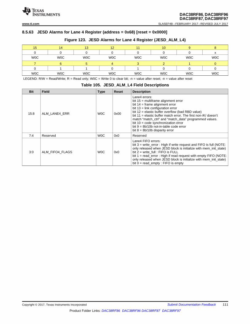
111
DAC38RF86, DAC38RF96DAC38RF87, DAC38RF97
www.ti.com SLASEF4B –FEBRUARY 2017–REVISED JULY 2017
Product Folder Links: DAC38RF86 DAC38RF96 DAC38RF87 DAC38RF97
Submit Documentation FeedbackCopyright © 2017, Texas Instruments Incorporated
8.5.63 JESD Alarms for Lane 4 Register (address = 0x68) [reset = 0x0000]
Figure 123. JESD Alarms for Lane 4 Register (JESD_ALM_L4)
15 14 13 12 11 10 9 80 0 0 0 0 0 0 x
W0C W0C W0C W0C W0C W0C W0C W0C
7 6 5 4 3 2 1 00 1 1 0 1 0 0 0
W0C W0C W0C W0C W0C W0C W0C W0CLEGEND: R/W = Read/Write; R = Read only; W0C = Write 0 to clear bit; -n = value after reset; -n = value after reset
Table 105. JESD_ALM_L4 Field DescriptionsBit Field Type Reset Description
15:8 ALM_LANE4_ERR W0C 0x00
Lane4 errors:bit 15 = multiframe alignment errorbit 14 = frame alignment errorbit 13 = link configuration errorbit 12 = elastic buffer overflow (bad RBD value)bit 11 = elastic buffer match error. The first non-/K/ doesn’tmatch “match_ctrl” and “match_data” programmed values.bit 10 = code synchronization errorbit 9 = 8b/10b not-in-table code errorbit 8 = 8b/10b disparity error
7:4 Reserved W0C 0x0 Reserved
3:0 ALM_FIFO4_FLAGS W0C 0x0
Lane4 FIFO errors:bit 3 = write_error : High if write request and FIFO is full (NOTE:only released when JESD block is initialize with mem_init_state)bit 2 = write_full : FIFO is FULLbit 1 = read_error : High if read request with empty FIFO (NOTE:only released when JESD block is initialize with mem_init_state)bit 0 = read_empty : FIFO is empty
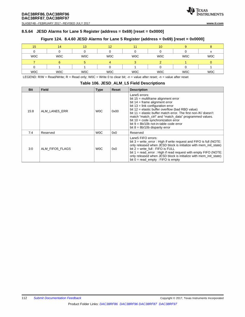
112
DAC38RF86, DAC38RF96DAC38RF87, DAC38RF97SLASEF4B –FEBRUARY 2017–REVISED JULY 2017 www.ti.com
Product Folder Links: DAC38RF86 DAC38RF96 DAC38RF87 DAC38RF97
Submit Documentation Feedback Copyright © 2017, Texas Instruments Incorporated
8.5.64 JESD Alarms for Lane 5 Register (address = 0x69) [reset = 0x0000]
Figure 124. 8.4.60 JESD Alarms for Lane 5 Register (address = 0x69) [reset = 0x0000]
15 14 13 12 11 10 9 80 0 0 0 0 0 0 x
W0C W0C W0C W0C W0C W0C W0C W0C
7 6 5 4 3 2 1 00 1 1 0 1 0 0 1
W0C W0C W0C W0C W0C W0C W0C W0CLEGEND: R/W = Read/Write; R = Read only; W0C = Write 0 to clear bit; -n = value after reset; -n = value after reset
Table 106. JESD_ALM_L5 Field DescriptionsBit Field Type Reset Description
15:8 ALM_LANE5_ERR W0C 0x00
Lane5 errors:bit 15 = multiframe alignment errorbit 14 = frame alignment errorbit 13 = link configuration errorbit 12 = elastic buffer overflow (bad RBD value)bit 11 = elastic buffer match error. The first non-/K/ doesn’tmatch “match_ctrl” and “match_data” programmed values.bit 10 = code synchronization errorbit 9 = 8b/10b not-in-table code errorbit 8 = 8b/10b disparity error
7:4 Reserved W0C 0x0 Reserved
3:0 ALM_FIFO5_FLAGS W0C 0x0
Lane5 FIFO errors:bit 3 = write_error : High if write request and FIFO is full (NOTE:only released when JESD block is initialize with mem_init_state)bit 2 = write_full : FIFO is FULLbit 1 = read_error : High if read request with empty FIFO (NOTE:only released when JESD block is initialize with mem_init_state)bit 0 = read_empty : FIFO is empty

113
DAC38RF86, DAC38RF96DAC38RF87, DAC38RF97
www.ti.com SLASEF4B –FEBRUARY 2017–REVISED JULY 2017
Product Folder Links: DAC38RF86 DAC38RF96 DAC38RF87 DAC38RF97
Submit Documentation FeedbackCopyright © 2017, Texas Instruments Incorporated
8.5.65 JESD Alarms for Lane 6 Register (address = 0x6A [reset = 0x0000]
Figure 125. JESD Alarms for Lane 6 Register (JESD_ALM_L6)
15 14 13 12 11 10 9 80 0 0 0 0 0 0 x
W0C W0C W0C W0C W0C W0C W0C W0C
7 6 5 4 3 2 1 00 1 1 0 1 0 1 0
W0C W0C W0C W0C W0C W0C W0C W0CLEGEND: R/W = Read/Write; R = Read only; W0C = Write 0 to clear bit; -n = value after reset; -n = value after reset
Table 107. JESD_ALM_L6 Field DescriptionsBit Field Type Reset Description
15:8 ALM_LANE6_ERR W0C 0x00
Lane6 errors:bit 15 = multiframe alignment errorbit 14 = frame alignment errorbit 13 = link configuration errorbit 12 = elastic buffer overflow (bad RBD value)bit 11 = elastic buffer match error. The first non-/K/ doesn’tmatch “match_ctrl” and “match_data” programmed values.bit 10 = code synchronization errorbit 9 = 8b/10b not-in-table code errorbit 8 = 8b/10b disparity error
7:4 Reserved W0C 0x0 Reserved
3:0 ALM_FIFO6_FLAGS W0C 0x0
Lane6 FIFO errors:bit 3 = write_error : High if write request and FIFO is full (NOTE:only released when JESD block is initialize with mem_init_state)bit 2 = write_full : FIFO is FULLbit 1 = read_error : High if read request with empty FIFO (NOTE:only released when JESD block is initialize with mem_init_state)bit 0 = read_empty : FIFO is empty
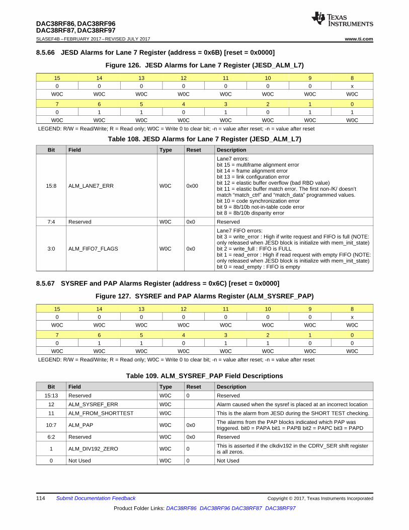
114
DAC38RF86, DAC38RF96DAC38RF87, DAC38RF97SLASEF4B –FEBRUARY 2017–REVISED JULY 2017 www.ti.com
Product Folder Links: DAC38RF86 DAC38RF96 DAC38RF87 DAC38RF97
Submit Documentation Feedback Copyright © 2017, Texas Instruments Incorporated
8.5.66 JESD Alarms for Lane 7 Register (address = 0x6B) [reset = 0x0000]
Figure 126. JESD Alarms for Lane 7 Register (JESD_ALM_L7)
15 14 13 12 11 10 9 80 0 0 0 0 0 0 x
W0C W0C W0C W0C W0C W0C W0C W0C
7 6 5 4 3 2 1 00 1 1 0 1 0 1 1
W0C W0C W0C W0C W0C W0C W0C W0CLEGEND: R/W = Read/Write; R = Read only; W0C = Write 0 to clear bit; -n = value after reset; -n = value after reset
Table 108. JESD Alarms for Lane 7 Register (JESD_ALM_L7)Bit Field Type Reset Description
15:8 ALM_LANE7_ERR W0C 0x00
Lane7 errors:bit 15 = multiframe alignment errorbit 14 = frame alignment errorbit 13 = link configuration errorbit 12 = elastic buffer overflow (bad RBD value)bit 11 = elastic buffer match error. The first non-/K/ doesn’tmatch “match_ctrl” and “match_data” programmed values.bit 10 = code synchronization errorbit 9 = 8b/10b not-in-table code errorbit 8 = 8b/10b disparity error
7:4 Reserved W0C 0x0 Reserved
3:0 ALM_FIFO7_FLAGS W0C 0x0
Lane7 FIFO errors:bit 3 = write_error : High if write request and FIFO is full (NOTE:only released when JESD block is initialize with mem_init_state)bit 2 = write_full : FIFO is FULLbit 1 = read_error : High if read request with empty FIFO (NOTE:only released when JESD block is initialize with mem_init_state)bit 0 = read_empty : FIFO is empty
8.5.67 SYSREF and PAP Alarms Register (address = 0x6C) [reset = 0x0000]
Figure 127. SYSREF and PAP Alarms Register (ALM_SYSREF_PAP)
15 14 13 12 11 10 9 80 0 0 0 0 0 0 x
W0C W0C W0C W0C W0C W0C W0C W0C
7 6 5 4 3 2 1 00 1 1 0 1 1 0 0
W0C W0C W0C W0C W0C W0C W0C W0CLEGEND: R/W = Read/Write; R = Read only; W0C = Write 0 to clear bit; -n = value after reset; -n = value after reset
Table 109. ALM_SYSREF_PAP Field DescriptionsBit Field Type Reset Description
15:13 Reserved W0C 0 Reserved12 ALM_SYSREF_ERR W0C Alarm caused when the sysref is placed at an incorrect location11 ALM_FROM_SHORTTEST W0C This is the alarm from JESD during the SHORT TEST checking.
10:7 ALM_PAP W0C 0x0 The alarms from the PAP blocks indicated which PAP wastriggered. bit0 = PAPA bit1 = PAPB bit2 = PAPC bit3 = PAPD
6:2 Reserved W0C 0x0 Reserved
1 ALM_DIV192_ZERO W0C 0 This is asserted if the clkdiv192 in the CDRV_SER shift registeris all zeros.
0 Not Used W0C 0 Not Used
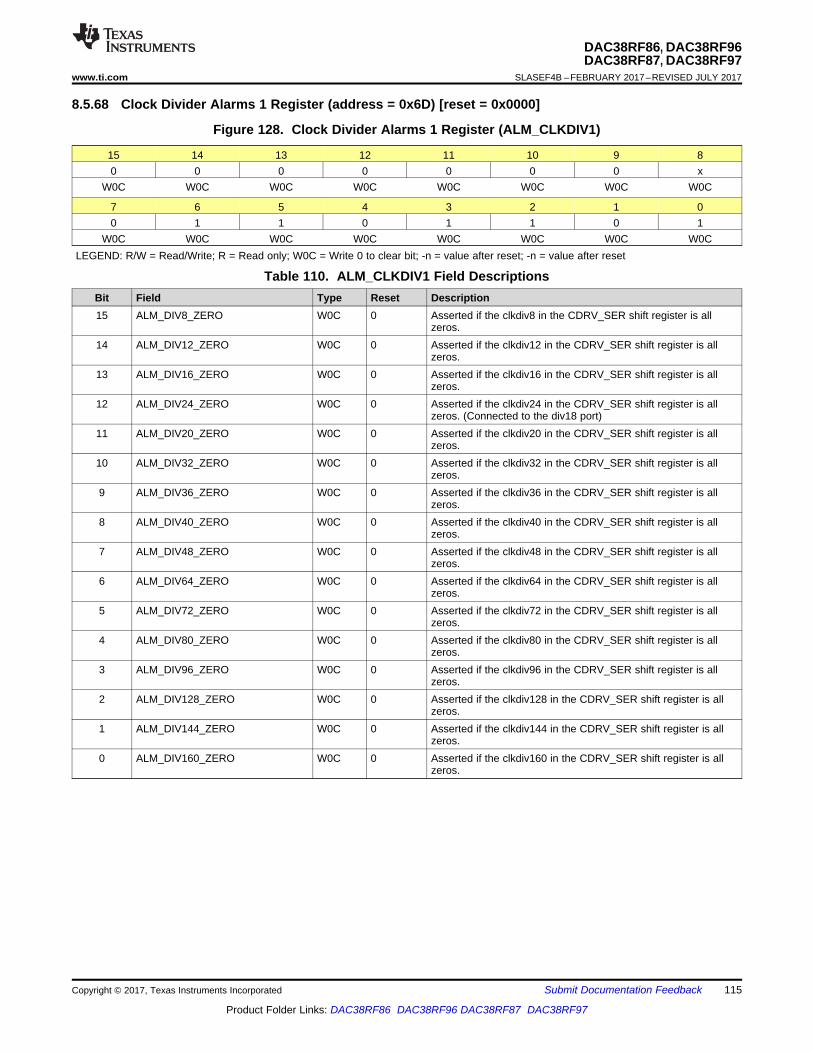
115
DAC38RF86, DAC38RF96DAC38RF87, DAC38RF97
www.ti.com SLASEF4B –FEBRUARY 2017–REVISED JULY 2017
Product Folder Links: DAC38RF86 DAC38RF96 DAC38RF87 DAC38RF97
Submit Documentation FeedbackCopyright © 2017, Texas Instruments Incorporated
8.5.68 Clock Divider Alarms 1 Register (address = 0x6D) [reset = 0x0000]
Figure 128. Clock Divider Alarms 1 Register (ALM_CLKDIV1)
15 14 13 12 11 10 9 80 0 0 0 0 0 0 x
W0C W0C W0C W0C W0C W0C W0C W0C
7 6 5 4 3 2 1 00 1 1 0 1 1 0 1
W0C W0C W0C W0C W0C W0C W0C W0CLEGEND: R/W = Read/Write; R = Read only; W0C = Write 0 to clear bit; -n = value after reset; -n = value after reset
Table 110. ALM_CLKDIV1 Field DescriptionsBit Field Type Reset Description15 ALM_DIV8_ZERO W0C 0 Asserted if the clkdiv8 in the CDRV_SER shift register is all
zeros.14 ALM_DIV12_ZERO W0C 0 Asserted if the clkdiv12 in the CDRV_SER shift register is all
zeros.13 ALM_DIV16_ZERO W0C 0 Asserted if the clkdiv16 in the CDRV_SER shift register is all
zeros.12 ALM_DIV24_ZERO W0C 0 Asserted if the clkdiv24 in the CDRV_SER shift register is all
zeros. (Connected to the div18 port)11 ALM_DIV20_ZERO W0C 0 Asserted if the clkdiv20 in the CDRV_SER shift register is all
zeros.10 ALM_DIV32_ZERO W0C 0 Asserted if the clkdiv32 in the CDRV_SER shift register is all
zeros.9 ALM_DIV36_ZERO W0C 0 Asserted if the clkdiv36 in the CDRV_SER shift register is all
zeros.8 ALM_DIV40_ZERO W0C 0 Asserted if the clkdiv40 in the CDRV_SER shift register is all
zeros.7 ALM_DIV48_ZERO W0C 0 Asserted if the clkdiv48 in the CDRV_SER shift register is all
zeros.6 ALM_DIV64_ZERO W0C 0 Asserted if the clkdiv64 in the CDRV_SER shift register is all
zeros.5 ALM_DIV72_ZERO W0C 0 Asserted if the clkdiv72 in the CDRV_SER shift register is all
zeros.4 ALM_DIV80_ZERO W0C 0 Asserted if the clkdiv80 in the CDRV_SER shift register is all
zeros.3 ALM_DIV96_ZERO W0C 0 Asserted if the clkdiv96 in the CDRV_SER shift register is all
zeros.2 ALM_DIV128_ZERO W0C 0 Asserted if the clkdiv128 in the CDRV_SER shift register is all
zeros.1 ALM_DIV144_ZERO W0C 0 Asserted if the clkdiv144 in the CDRV_SER shift register is all
zeros.0 ALM_DIV160_ZERO W0C 0 Asserted if the clkdiv160 in the CDRV_SER shift register is all
zeros.
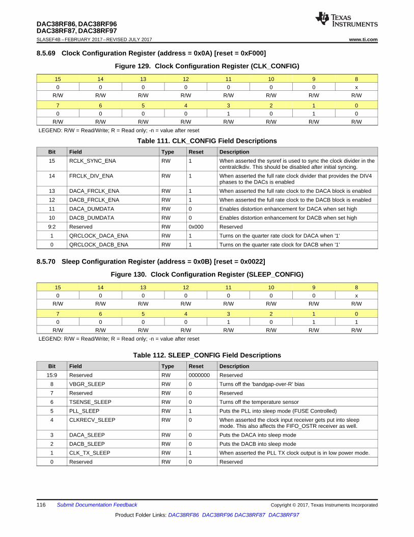
116
DAC38RF86, DAC38RF96DAC38RF87, DAC38RF97SLASEF4B –FEBRUARY 2017–REVISED JULY 2017 www.ti.com
Product Folder Links: DAC38RF86 DAC38RF96 DAC38RF87 DAC38RF97
Submit Documentation Feedback Copyright © 2017, Texas Instruments Incorporated
8.5.69 Clock Configuration Register (address = 0x0A) [reset = 0xF000]
Figure 129. Clock Configuration Register (CLK_CONFIG)
15 14 13 12 11 10 9 80 0 0 0 0 0 0 x
R/W R/W R/W R/W R/W R/W R/W R/W
7 6 5 4 3 2 1 00 0 0 0 1 0 1 0
R/W R/W R/W R/W R/W R/W R/W R/WLEGEND: R/W = Read/Write; R = Read only; -n = value after reset
Table 111. CLK_CONFIG Field DescriptionsBit Field Type Reset Description15 RCLK_SYNC_ENA RW 1 When asserted the sysref is used to sync the clock divider in the
centralclkdiv. This should be disabled after initial syncing.14 FRCLK_DIV_ENA RW 1 When asserted the full rate clock divider that provides the DIV4
phases to the DACs is enabled13 DACA_FRCLK_ENA RW 1 When asserted the full rate clock to the DACA block is enabled12 DACB_FRCLK_ENA RW 1 When asserted the full rate clock to the DACB block is enabled11 DACA_DUMDATA RW 0 Enables distortion enhancement for DACA when set high10 DACB_DUMDATA RW 0 Enables distortion enhancement for DACB when set high9:2 Reserved RW 0x000 Reserved1 QRCLOCK_DACA_ENA RW 1 Turns on the quarter rate clock for DACA when '1'0 QRCLOCK_DACB_ENA RW 1 Turns on the quarter rate clock for DACB when '1'
8.5.70 Sleep Configuration Register (address = 0x0B) [reset = 0x0022]
Figure 130. Clock Configuration Register (SLEEP_CONFIG)
15 14 13 12 11 10 9 80 0 0 0 0 0 0 x
R/W R/W R/W R/W R/W R/W R/W R/W
7 6 5 4 3 2 1 00 0 0 0 1 0 1 1
R/W R/W R/W R/W R/W R/W R/W R/WLEGEND: R/W = Read/Write; R = Read only; -n = value after reset
Table 112. SLEEP_CONFIG Field DescriptionsBit Field Type Reset Description
15:9 Reserved RW 0000000 Reserved8 VBGR_SLEEP RW 0 Turns off the 'bandgap-over-R' bias7 Reserved RW 0 Reserved6 TSENSE_SLEEP RW 0 Turns off the temperature sensor5 PLL_SLEEP RW 1 Puts the PLL into sleep mode (FUSE Controlled)4 CLKRECV_SLEEP RW 0 When asserted the clock input receiver gets put into sleep
mode. This also affects the FIFO_OSTR receiver as well.3 DACA_SLEEP RW 0 Puts the DACA into sleep mode2 DACB_SLEEP RW 0 Puts the DACB into sleep mode1 CLK_TX_SLEEP RW 1 When asserted the PLL TX clock output is in low power mode.0 Reserved RW 0 Reserved
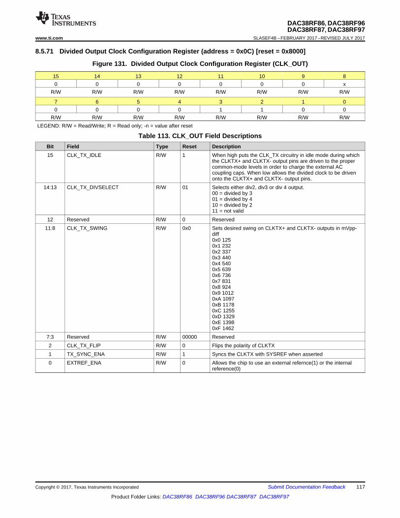
117
DAC38RF86, DAC38RF96DAC38RF87, DAC38RF97
www.ti.com SLASEF4B –FEBRUARY 2017–REVISED JULY 2017
Product Folder Links: DAC38RF86 DAC38RF96 DAC38RF87 DAC38RF97
Submit Documentation FeedbackCopyright © 2017, Texas Instruments Incorporated
8.5.71 Divided Output Clock Configuration Register (address = 0x0C) [reset = 0x8000]
Figure 131. Divided Output Clock Configuration Register (CLK_OUT)
15 14 13 12 11 10 9 80 0 0 0 0 0 0 x
R/W R/W R/W R/W R/W R/W R/W R/W
7 6 5 4 3 2 1 00 0 0 0 1 1 0 0
R/W R/W R/W R/W R/W R/W R/W R/WLEGEND: R/W = Read/Write; R = Read only; -n = value after reset
Table 113. CLK_OUT Field DescriptionsBit Field Type Reset Description15 CLK_TX_IDLE R/W 1 When high puts the CLK_TX circuitry in idle mode during which
the CLKTX+ and CLKTX- output pins are driven to the propercommon-mode levels in order to charge the external ACcoupling caps. When low allows the divided clock to be drivenonto the CLKTX+ and CLKTX- output pins.
14:13 CLK_TX_DIVSELECT R/W 01 Selects either div2, div3 or div 4 output.00 = divided by 301 = divided by 410 = divided by 211 = not valid
12 Reserved R/W 0 Reserved11:8 CLK_TX_SWING R/W 0x0 Sets desired swing on CLKTX+ and CLKTX- outputs in mVpp-
diff0x0 1250x1 2320x2 3370x3 4400x4 5400x5 6390x6 7360x7 8310x8 9240x9 10120xA 10970xB 11780xC 12550xD 13290xE 13980xF 1462
7:3 Reserved R/W 00000 Reserved2 CLK_TX_FLIP R/W 0 Flips the polarity of CLKTX1 TX_SYNC_ENA R/W 1 Syncs the CLKTX with SYSREF when asserted0 EXTREF_ENA R/W 0 Allows the chip to use an external refernce(1) or the internal
reference(0)
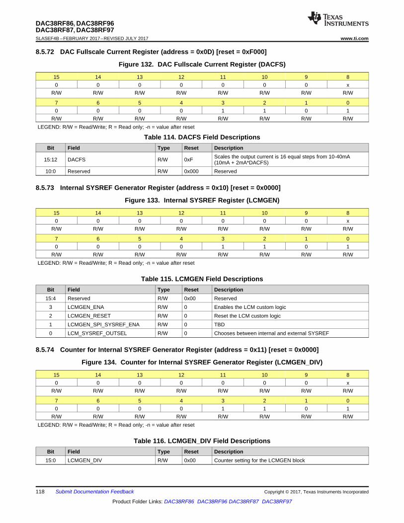
118
DAC38RF86, DAC38RF96DAC38RF87, DAC38RF97SLASEF4B –FEBRUARY 2017–REVISED JULY 2017 www.ti.com
Product Folder Links: DAC38RF86 DAC38RF96 DAC38RF87 DAC38RF97
Submit Documentation Feedback Copyright © 2017, Texas Instruments Incorporated
8.5.72 DAC Fullscale Current Register (address = 0x0D) [reset = 0xF000]
Figure 132. DAC Fullscale Current Register (DACFS)
15 14 13 12 11 10 9 80 0 0 0 0 0 0 x
R/W R/W R/W R/W R/W R/W R/W R/W
7 6 5 4 3 2 1 00 0 0 0 1 1 0 1
R/W R/W R/W R/W R/W R/W R/W R/WLEGEND: R/W = Read/Write; R = Read only; -n = value after reset
Table 114. DACFS Field DescriptionsBit Field Type Reset Description
15:12 DACFS R/W 0xF Scales the output current is 16 equal steps from 10-40mA(10mA + 2mA*DACFS)
10:0 Reserved R/W 0x000 Reserved
8.5.73 Internal SYSREF Generator Register (address = 0x10) [reset = 0x0000]
Figure 133. Internal SYSREF Register (LCMGEN)
15 14 13 12 11 10 9 80 0 0 0 0 0 0 x
R/W R/W R/W R/W R/W R/W R/W R/W
7 6 5 4 3 2 1 00 0 0 0 1 1 0 1
R/W R/W R/W R/W R/W R/W R/W R/WLEGEND: R/W = Read/Write; R = Read only; -n = value after reset
Table 115. LCMGEN Field DescriptionsBit Field Type Reset Description
15:4 Reserved R/W 0x00 Reserved3 LCMGEN_ENA R/W 0 Enables the LCM custom logic2 LCMGEN_RESET R/W 0 Reset the LCM custom logic1 LCMGEN_SPI_SYSREF_ENA R/W 0 TBD0 LCM_SYSREF_OUTSEL R/W 0 Chooses between internal and external SYSREF
8.5.74 Counter for Internal SYSREF Generator Register (address = 0x11) [reset = 0x0000]
Figure 134. Counter for Internal SYSREF Generator Register (LCMGEN_DIV)
15 14 13 12 11 10 9 80 0 0 0 0 0 0 x
R/W R/W R/W R/W R/W R/W R/W R/W
7 6 5 4 3 2 1 00 0 0 0 1 1 0 1
R/W R/W R/W R/W R/W R/W R/W R/WLEGEND: R/W = Read/Write; R = Read only; -n = value after reset
Table 116. LCMGEN_DIV Field DescriptionsBit Field Type Reset Description
15:0 LCMGEN_DIV R/W 0x00 Counter setting for the LCMGEN block
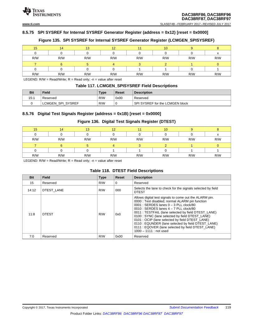
119
DAC38RF86, DAC38RF96DAC38RF87, DAC38RF97
www.ti.com SLASEF4B –FEBRUARY 2017–REVISED JULY 2017
Product Folder Links: DAC38RF86 DAC38RF96 DAC38RF87 DAC38RF97
Submit Documentation FeedbackCopyright © 2017, Texas Instruments Incorporated
8.5.75 SPI SYSREF for Internal SYSREF Generator Register (address = 0x12) [reset = 0x0000]
Figure 135. SPI SYSREF for Internal SYSREF Generator Register (LCMGEN_SPISYSREF)
15 14 13 12 11 10 9 80 0 0 0 0 0 0 x
R/W R/W R/W R/W R/W R/W R/W R/W
7 6 5 4 3 2 1 00 0 0 0 1 1 0 1
R/W R/W R/W R/W R/W R/W R/W R/WLEGEND: R/W = Read/Write; R = Read only; -n = value after reset
Table 117. LCMGEN_SPISYSREF Field DescriptionsBit Field Type Reset Description
15:1 Reserved R/W 0x00 Reserved0 LCMGEN_SPI_SYSREF R/W 0 SPI SYSREF for the LCMGEN block
8.5.76 Digital Test Signals Register (address = 0x1B) [reset = 0x0000]
Figure 136. Digital Test Signals Register (DTEST)
15 14 13 12 11 10 9 80 0 0 0 0 0 0 x
R/W R/W R/W R/W R/W R/W R/W R/W
7 6 5 4 3 2 1 00 0 0 1 1 0 1 1
R/W R/W R/W R/W R/W R/W R/W R/WLEGEND: R/W = Read/Write; R = Read only; -n = value after reset
Table 118. DTEST Field DescriptionsBit Field Type Reset Description15 Reserved R/W 0 Reserved
14:12 DTEST_LANE R/W 000 Selects the lane to check for the signals selected by fieldDTEST
11:8 DTEST R/W 0x0
Allows digital test signals to come out the ALARM pin.0000 : Test disabled; normal ALARM pin function0001 : SERDES lanes 0 – 3 PLL clock/800010 : SERDES lanes 4 – 7 PLL clock/800011 : TESTFAIL (lane selected by field DTEST_LANE)0100 : SYNC (lane selected by field DTEST_LANE)0101 : OCIP (lane selected by field DTEST_LANE)0110 : EQUNDER (lane selected by field DTEST_LANE)0111 : EQOVER (lane selected by field DTEST_LANE)1000 – 1111 : not used
7:0 Reserved R/W 0x00 Reserved

120
DAC38RF86, DAC38RF96DAC38RF87, DAC38RF97SLASEF4B –FEBRUARY 2017–REVISED JULY 2017 www.ti.com
Product Folder Links: DAC38RF86 DAC38RF96 DAC38RF87 DAC38RF97
Submit Documentation Feedback Copyright © 2017, Texas Instruments Incorporated
8.5.77 Sleep Pin Control Register (address = 0x23) [reset = 0xFFFF]These fields control the routing of the SLEEP signal to different blocks. Assertion means that the SLEEP signalwill be sent to the block. These bits do not override the SPI bits; just the SLEEP signal from the PAD.
Figure 137. Sleep Pin Control Register (SLEEP_CNTL)
15 14 13 12 11 10 9 80 0 0 0 0 0 0 x
R/W R/W R/W R/W R/W R/W R/W R/W
7 6 5 4 3 2 1 00 0 1 0 0 0 1 1
R/W R/W R/W R/W R/W R/W R/W R/WLEGEND: R/W = Read/Write; R = Read only; -n = value after reset
Table 119. SLEEP_CNTL Field DescriptionsBit Field Type Reset Description
15:10 Reserved R/W 11111 Reserved9 CLKOUT_SLEEP R/W 1 Allows the output clock to sleep8 BG_SLEEP R/W 1 Allows the band gap to sleep7 TEMP_SLEEP R/W 1 Allows the temp sensor to sleep6 PLL_CP_SLEEP R/W 1 Allows the PLL charge pump to sleep5 PLL_SLEEP R/W 1 Allows the PLL to sleep4 CLK_RECV_SLEEP R/W 1 Allows the clock receiver to sleep
3:2 Reserved R/W 11 Reserved1 DACB_SLEEP R/W 1 Allows DACB to sleep0 DACA_SLEEP R/W 1 Allows DACA to sleep
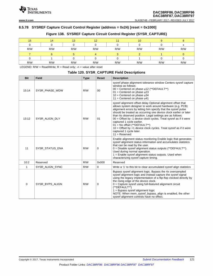
121
DAC38RF86, DAC38RF96DAC38RF87, DAC38RF97
www.ti.com SLASEF4B –FEBRUARY 2017–REVISED JULY 2017
Product Folder Links: DAC38RF86 DAC38RF96 DAC38RF87 DAC38RF97
Submit Documentation FeedbackCopyright © 2017, Texas Instruments Incorporated
8.5.78 SYSREF Capture Circuit Control Register (address = 0x24) [reset = 0x1000]
Figure 138. SYSREF Capture Circuit Control Register (SYSR_CAPTURE)
15 14 13 12 11 10 9 80 0 0 0 0 0 0 x
R/W R/W R/W R/W R/W R/W R/W R/W
7 6 5 4 3 2 1 00 1 0 0 0 1 0 0
R/W R/W R/W R/W R/W R/W R/W R/WLEGEND: R/W = Read/Write; R = Read only; -n = value after reset
Table 120. SYSR_CAPTURE Field DescriptionsBit Field Type Reset Description
15:14 SYSR_PHASE_WDW R/W 00
sysref phase alignment tolerance window Centers sysref capturewindow as follows:00 = Centered on phase φ12 (**DEFAULT**)01 = Centered on phase φ2310 = Centered on phase φ3411 = Centered on phase φ41
13:12 SYSR_ALIGN_DLY R/W 01
sysref alignment offset delay Optional alignment offset thatallows system designer to work around hardware (e.g. PCB)alignment errors by letting him specify that the sysref pulseshould be treated as occurring one device clock earlier or laterthan its observed position. Legal settings are as follows:00 = Offset by -1 device clock cycles. Treat sysref as if it werecaptured 1 cycle earlier.01 = No offset (**DEFAULT**)10 = Offset by +1 device clock cycles. Treat sysref as if it werecaptured 1 cycle later.11 = Reserved
11 SYSR_STATUS_ENA R/W 0
Enable alignment status monitoring Enable logic that generatessysref alignment status information and accumulates statisticsthat can be read by the user.0 = Disable sysref alignment status outputs (**DEFAULT**).Used during normal operation.1 = Enable sysref alignment status outputs. Used whencharacterizing sysref capture timing.
10:2 Reserved R/W 0x000 Reserved1 SYSR_ALIGN_SYNC R/W 0 Write a ‘1’ to this bit to clear accumulated sysref align statistics
0 SYSR_BYPS_ALIGN R/W 0
Bypass sysref alignment logic. Bypass the 4x oversampledsysref alignment logic and instead capture the sysref signalusing the legacy implementation of a flip-flop clocked directly bythe rising edge of the device clock.0 = Capture sysref using full-featured alignment circuit(**DEFAULT**)1 = Bypass sysref alignment logicNOTE: When mem_sysref_bypass_align is enabled, the othersysref alignment controls have no effect.

122
DAC38RF86, DAC38RF96DAC38RF87, DAC38RF97SLASEF4B –FEBRUARY 2017–REVISED JULY 2017 www.ti.com
Product Folder Links: DAC38RF86 DAC38RF96 DAC38RF87 DAC38RF97
Submit Documentation Feedback Copyright © 2017, Texas Instruments Incorporated
8.5.79 Clock Input and PLL Configuration Register (address = 0x31) [reset = 0x0200]
Figure 139. Clock Input and PLL Configuration Register (CLK_PLL_CFG)
15 14 13 12 11 10 9 80 0 0 0 0 0 0 x
R/W R/W R/W R/W R/W R/W R/W R/W
7 6 5 4 3 2 1 00 0 1 1 0 0 0 1
R/W R/W R/W R/W R/W R/W R/W R/WLEGEND: R/W = Read/Write; R = Read only; -n = value after reset
Table 121. Clock Input and PLL Configuration Register (CLK_PLL_CFG)Bit Field Type Reset Description
15:14 Reserved R/W 00 Reserved
13 SEL_EXTCLK_DIFFSE R/W 0
Selects the external differential or single ended clock forDACCLK.0 = differential1 = single ended
12 PLL_RESET R/W 0 When set the M divider; N divider and PFD are held reset
11 PLL_NDIVSYNC_ENA R/W 0 When asserted; the SYSREF input is used to sync the Ndividers of the PLL.
10 PLL_ENA R/W 0
Enables the PLL output as the DAC clock when set; the clockprovided at the DACCLKP/N is used as the PLL reference clock.When cleared; the PLL is bypassed and the clock provided atthe DACCLKP/N pins is used as the DAC clock
9 PLL_CP_SLEEP R/W 1Must be set to '0' for proper PLL operation.1 = Charge pump is put to sleep and can be driven by externalsource through the ATEST pins.
8 Reserved R/W 0 Reserved7:3 PLL_N_M1 R/W 00000 Reference clock divider; divide by is N+1
2:0 LOCKDET_ADJ R/W 000 Adjusts the lock detector sensitivity. Upper bit isn't used:x00 - highest sensitivity x11 - lowest sensitivity
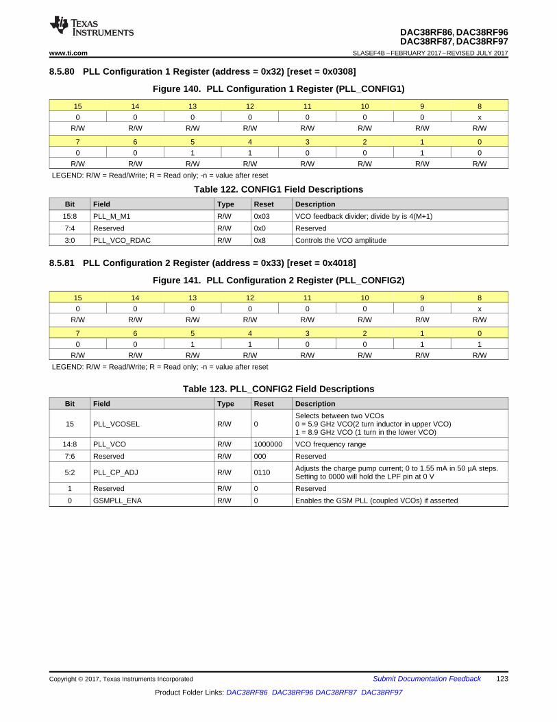
123
DAC38RF86, DAC38RF96DAC38RF87, DAC38RF97
www.ti.com SLASEF4B –FEBRUARY 2017–REVISED JULY 2017
Product Folder Links: DAC38RF86 DAC38RF96 DAC38RF87 DAC38RF97
Submit Documentation FeedbackCopyright © 2017, Texas Instruments Incorporated
8.5.80 PLL Configuration 1 Register (address = 0x32) [reset = 0x0308]
Figure 140. PLL Configuration 1 Register (PLL_CONFIG1)
15 14 13 12 11 10 9 80 0 0 0 0 0 0 x
R/W R/W R/W R/W R/W R/W R/W R/W
7 6 5 4 3 2 1 00 0 1 1 0 0 1 0
R/W R/W R/W R/W R/W R/W R/W R/WLEGEND: R/W = Read/Write; R = Read only; -n = value after reset
Table 122. CONFIG1 Field DescriptionsBit Field Type Reset Description
15:8 PLL_M_M1 R/W 0x03 VCO feedback divider; divide by is 4(M+1)7:4 Reserved R/W 0x0 Reserved3:0 PLL_VCO_RDAC R/W 0x8 Controls the VCO amplitude
8.5.81 PLL Configuration 2 Register (address = 0x33) [reset = 0x4018]
Figure 141. PLL Configuration 2 Register (PLL_CONFIG2)
15 14 13 12 11 10 9 80 0 0 0 0 0 0 x
R/W R/W R/W R/W R/W R/W R/W R/W
7 6 5 4 3 2 1 00 0 1 1 0 0 1 1
R/W R/W R/W R/W R/W R/W R/W R/WLEGEND: R/W = Read/Write; R = Read only; -n = value after reset
Table 123. PLL_CONFIG2 Field DescriptionsBit Field Type Reset Description
15 PLL_VCOSEL R/W 0Selects between two VCOs0 = 5.9 GHz VCO(2 turn inductor in upper VCO)1 = 8.9 GHz VCO (1 turn in the lower VCO)
14:8 PLL_VCO R/W 1000000 VCO frequency range7:6 Reserved R/W 000 Reserved
5:2 PLL_CP_ADJ R/W 0110 Adjusts the charge pump current; 0 to 1.55 mA in 50 µA steps.Setting to 0000 will hold the LPF pin at 0 V
1 Reserved R/W 0 Reserved0 GSMPLL_ENA R/W 0 Enables the GSM PLL (coupled VCOs) if asserted

124
DAC38RF86, DAC38RF96DAC38RF87, DAC38RF97SLASEF4B –FEBRUARY 2017–REVISED JULY 2017 www.ti.com
Product Folder Links: DAC38RF86 DAC38RF96 DAC38RF87 DAC38RF97
Submit Documentation Feedback Copyright © 2017, Texas Instruments Incorporated
8.5.82 LVDS Output Configuration Register (address = 0x34) [reset = 0x0000]
Figure 142. LVDS Output Configuration Register (LVDS_CONFIG)
15 14 13 12 11 10 9 80 0 0 0 0 0 0 x
R/W R/W R/W R/W R/W R/W R/W R/W
7 6 5 4 3 2 1 00 0 1 1 0 1 0 0
R/W R/W R/W R/W R/W R/W R/W R/WLEGEND: R/W = Read/Write; R = Read only; -n = value after reset
Table 124. LVDS_CONFIG Field DescriptionsBit Field Type Reset Description
15 LVDS_LOPWRB R/W 0 LVDS Output current control LSB; allows output current to bescaled from ~2 mA to ~4 mA
14 LVDS_LOPWRA R/W 0 LVDS Output current control MSB; allows output current to bescaled from ~2 mA to ~4 mA
13 LVDS_LPSEL R/W 0
SYNC LVDS output on chip termination control; 100 Ω whencleared; 200 ΩOutput current settings for the combination of bits 15:13110 = 4.00 mA010 = 3.50 mA100 = 3.00 mA000 = 2.50 mA – Default current111 = 4.00 mA011 = 3.33 mA101 = 2.66 mA001 = 2.00 mA
12 LVDS_EFUSE_SEL R/W 0 Enable LVDS bias bandgap reference voltage to the ATESTmultiplexer.
11:10 LVDS_TRIM R/W 00
Adjusts the LVDS 1.2 V reference. LVDS_TRIM_ENA must beset and LVDS_EFUSE_SEL must be cleared for these bits tohave any effect.10 +70 mV00 -70 mV01 default11 -20 mV.
9 LVDS_TRIM_ENA R/W 0When set and LVDS_EFUSE_SEL is cleared; the LVDS_TRIMadjustment is enabled. When cleared; the LVDS_TRIM has noeffect.
8 LVDS_SYNC0\_PD R/W 0 The SYNC0 LVDS output is in power down.7 Reserved R/W 0 Reserved
6 LVDS_SYNC0\_CM R/W 0 SYNC0 LVDS output common mode is 1.2 V when cleared; 0.9V when set.
5:0 Reserved R/W 0x00 Reserved
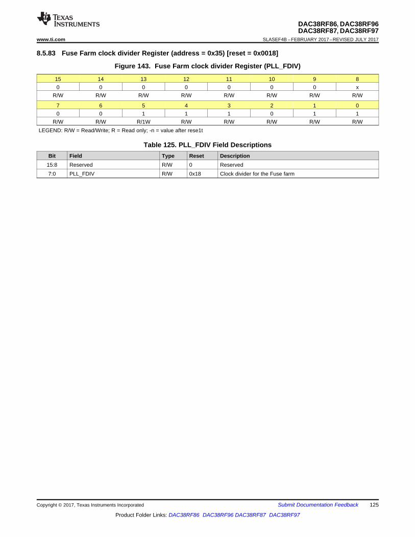
125
DAC38RF86, DAC38RF96DAC38RF87, DAC38RF97
www.ti.com SLASEF4B –FEBRUARY 2017–REVISED JULY 2017
Product Folder Links: DAC38RF86 DAC38RF96 DAC38RF87 DAC38RF97
Submit Documentation FeedbackCopyright © 2017, Texas Instruments Incorporated
8.5.83 Fuse Farm clock divider Register (address = 0x35) [reset = 0x0018]
Figure 143. Fuse Farm clock divider Register (PLL_FDIV)
15 14 13 12 11 10 9 80 0 0 0 0 0 0 x
R/W R/W R/W R/W R/W R/W R/W R/W
7 6 5 4 3 2 1 00 0 1 1 1 0 1 1
R/W R/W R/1W R/W R/W R/W R/W R/WLEGEND: R/W = Read/Write; R = Read only; -n = value after rese1t
Table 125. PLL_FDIV Field DescriptionsBit Field Type Reset Description
15:8 Reserved R/W 0 Reserved7:0 PLL_FDIV R/W 0x18 Clock divider for the Fuse farm
126
DAC38RF86, DAC38RF96DAC38RF87, DAC38RF97SLASEF4B –FEBRUARY 2017–REVISED JULY 2017 www.ti.com
Product Folder Links: DAC38RF86 DAC38RF96 DAC38RF87 DAC38RF97
Submit Documentation Feedback Copyright © 2017, Texas Instruments Incorporated
8.5.84 Serdes Clock Configuration Register (address = 0x3B) [reset = 0x0002]
Figure 144. Serdes Clock Configuration Register (SRDS_CLK_CFG)
15 14 13 12 11 10 9 80 0 0 0 0 0 0 x
R/W R/W R/W R/W R/W R/W R/W R/W
7 6 5 4 3 2 1 00 0 1 1 1 0 1 1
R/W R/W R/1W R/W R/W R/W R/W R/WLEGEND: R/W = Read/Write; R = Read only; -n = value after rese1t
Table 126. SRDS_CLK_CFG Field DescriptionsBit Field Type Reset Description
15 SERDES_CLK_SEL R/W 0Select either the PLL output of the DACCLK from the pad.0 = DACCLK pad1 = PLL output
14:11 SERDES_REFCLK_DIV R/W 0x0 The divide amount for the serdes REFCLK minus 110:2 Reserved R/W 0x000 Reserved
1:0 SERDES_REFCLK_PREDIV R/W 10
These bits select the pre-divide on the DACCLK input clockbefore the DACCLK is used in the dividers used in the SERDESPLL REFCLK and the Fusefarm SYSCLK.00 = if DACCLK input ≤ 2 GHz; prediv is set to div101 = if DACCLK input is ≤ 4 GHz and > 2 GHz, prediv is set todiv210 = if DACCLK input is ≤ 9 GHz and > 4 GHz, prediv is set todiv411 = Not valid
8.5.85 Serdes PLL Configuration Register (address = 0x3C) [reset = 0x8228]
Figure 145. Serdes PLL Configuration Register (SRDS_PLL_CFG)
15 14 13 12 11 10 9 80 0 0 0 0 0 0 x
R/W R/W R/W R/W R/W R/W R/W R/W
7 6 5 4 3 2 1 00 0 1 1 1 1 0 0
R/W R/W R/W R/W R/W R/W R/W R/WLEGEND: R/W = Read/Write; R = Read only; -n = value after reset
Table 127. SRDS_PLL_CFG Field DescriptionsBit Field Type Reset Description15 ENDIVCLK R/W 1 Enable divided by 5 output clock
14:3 CLKBYP R/W 00 Serdes clock bypass12:11 LB R/W 00 Serdes PLL loop bandwidth
10 SLEEPPLL R/W 0 Serdes PLL Sleep9 VRANGE R/W 1 Serdes PLL loop filter range
8:1 MPY R/W 00010100 Serdes reference clock multiply factor0 CORRECT R/W 0 AND'ed with LANE_ENA so it must be set to 1 for correct
behavior

127
DAC38RF86, DAC38RF96DAC38RF87, DAC38RF97
www.ti.com SLASEF4B –FEBRUARY 2017–REVISED JULY 2017
Product Folder Links: DAC38RF86 DAC38RF96 DAC38RF87 DAC38RF97
Submit Documentation FeedbackCopyright © 2017, Texas Instruments Incorporated
8.5.86 Serdes Configuration 1 Register (address = 0x3D) [reset = 0x0x0088]
Figure 146. Serdes Configuration 1 Register (SRDS_CFG1)
15 14 13 12 11 10 9 80 0 0 0 0 0 0 x
R/W R/W R/W R/W R/W R/W R/W R/W
7 6 5 4 3 2 1 00 0 1 1 1 1 0 1
R/W R/W R/W R/W R/W R/W R/W R/WLEGEND: R/W = Read/Write; R = Read only; -n = value after reset
Table 128. RDS_CFG1 Field DescriptionsBit Field Type Reset Description15 Reserved R/W 0 Reserved
14:12 TESTPATT R/W 000 Test pattern11 BSINRXN R/W 0 Enable boundary scan - pins10 BSINRXP R/W 0 Enable boundary scan + pins9:8 Reserved R/W 00 Reserved7 ENOC R/W 1 Enable Serdes offset compensation6 EQHLD R/W 0 Equalizer hold
5:3 EQ R/W 001 Serdes equalizer2:0 CDR R/W 000 Clock data recovery algorithm settings

128
DAC38RF86, DAC38RF96DAC38RF87, DAC38RF97SLASEF4B –FEBRUARY 2017–REVISED JULY 2017 www.ti.com
Product Folder Links: DAC38RF86 DAC38RF96 DAC38RF87 DAC38RF97
Submit Documentation Feedback Copyright © 2017, Texas Instruments Incorporated
8.5.87 Serdes Configuration 2 Register (address = 0x3E) [reset = 0x0x0909]
Figure 147. Serdes Configuration 2 Register (SRDS_CFG2)
15 14 13 12 11 10 9 80 0 0 0 0 0 0 x
R/W R/W R/W R/W R/W R/W R/W R/W
7 6 5 4 3 2 1 00 0 1 1 1 1 1 0
R/W R/W R/W R/W R/W R/W R/W R/WLEGEND: R/W = Read/Write; R = Read only; -n = value after reset
Table 129. SRDS_CFG2 Field DescriptionsBit Field Type Reset Description
15:13 LOS R/W 000
Enables loss of signal detection.000 - Enable detection100 - Disable detectionother - reserved
12:11 ALIGN R/W 01
Enables external or internal symbol alignment00 : Disabled01 : Comma alignment10: Align jog
10:8 TERM R/W 001
Valid programming:001 – AC coupling with common mode = 0.7 V100 – 0 V common mode.101 – 0.25 V common mode111 – DC coupling with common mode of 0.6 V.(NOTE: This is not compatible with JESD)
7 Reserved R/W 0 Reserved
6:5 RATE R/W 00 Selects full (00), half (01), quarter (10) or eighth (11) rateoperation.
4:2 BUSWIDTH R/W 010Selects the parallel interface width (16 or 20 bits).0 : 20 bits1: 16 bits
1 SLEEPRX R/W 0 Powers the receiver down into the sleep (fast power up) statewhen high.
0 Reserved R/W 1 Reserved
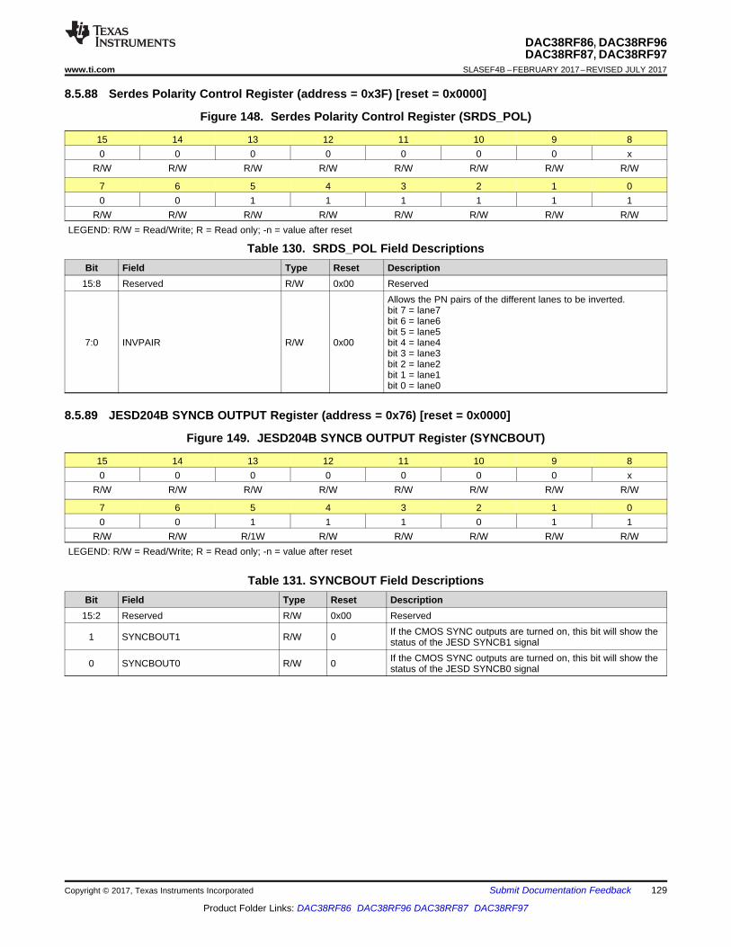
129
DAC38RF86, DAC38RF96DAC38RF87, DAC38RF97
www.ti.com SLASEF4B –FEBRUARY 2017–REVISED JULY 2017
Product Folder Links: DAC38RF86 DAC38RF96 DAC38RF87 DAC38RF97
Submit Documentation FeedbackCopyright © 2017, Texas Instruments Incorporated
8.5.88 Serdes Polarity Control Register (address = 0x3F) [reset = 0x0000]
Figure 148. Serdes Polarity Control Register (SRDS_POL)
15 14 13 12 11 10 9 80 0 0 0 0 0 0 x
R/W R/W R/W R/W R/W R/W R/W R/W
7 6 5 4 3 2 1 00 0 1 1 1 1 1 1
R/W R/W R/W R/W R/W R/W R/W R/WLEGEND: R/W = Read/Write; R = Read only; -n = value after reset
Table 130. SRDS_POL Field DescriptionsBit Field Type Reset Description
15:8 Reserved R/W 0x00 Reserved
7:0 INVPAIR R/W 0x00
Allows the PN pairs of the different lanes to be inverted.bit 7 = lane7bit 6 = lane6bit 5 = lane5bit 4 = lane4bit 3 = lane3bit 2 = lane2bit 1 = lane1bit 0 = lane0
8.5.89 JESD204B SYNCB OUTPUT Register (address = 0x76) [reset = 0x0000]
Figure 149. JESD204B SYNCB OUTPUT Register (SYNCBOUT)
15 14 13 12 11 10 9 80 0 0 0 0 0 0 x
R/W R/W R/W R/W R/W R/W R/W R/W
7 6 5 4 3 2 1 00 0 1 1 1 0 1 1
R/W R/W R/1W R/W R/W R/W R/W R/WLEGEND: R/W = Read/Write; R = Read only; -n = value after reset
Table 131. SYNCBOUT Field DescriptionsBit Field Type Reset Description
15:2 Reserved R/W 0x00 Reserved
1 SYNCBOUT1 R/W 0 If the CMOS SYNC outputs are turned on, this bit will show thestatus of the JESD SYNCB1 signal
0 SYNCBOUT0 R/W 0 If the CMOS SYNC outputs are turned on, this bit will show thestatus of the JESD SYNCB0 signal

PULL TXENABLE LOW
x� Provide all 1V supply rails, 1.8V rails and -1.8V rail.
x� Pull TRSTB pin of the JTAG port low
x� Provide a clock to the differential or single ended clock input
x� Toggle RESETB pin low then high (recommended pulse duration
>10us)
Read SPI Page 0, Register 0x7F
Configure the SPI resgisters for the desired mode
Bits[15:10]=10000b
On chip PLL mode
Start SYSREF Generation
NO
Read page 0, address 0x06
Tj = bits[15:8]
LFVOLT = bits[7:5]
Increment/decrement
VCO tune value
SPI Page 4, address
0x33, bits[14:8]
108��G��di�< 125C, LFVOLT =5or6
92��G�di�< 108C, LFVOLT=4or5
26��G�di�< 92C, LFVOLT =3or4
-40��G�di�< 26C, LFVOLT =2or3
YES
x� Reset encoder block:
Page 1/2:address 0x24:bits [6:4] = 000b
Page 1/2:address 0x5C:bits [2:0] = 000b
Page 4:address 0x0A:bit [15] = 1b
Ensure at least 2 SYSREF rising edges occur to reset the encoder
Page 4:address 0x0A:bit [15] = 0b
x� Put JESD204B core in reset
Page 0:address 0x00:bits [1:0] = 11b
x� Sync CDRV and JESD204B blocks
Page 1/2:address 0x24:bits [6:4] = 010b
Ensure at least 2 SYSREF rising edges occur to reset the CDRV
Page 1/2:address 0x5C:bits [2:0] = 011b
Ensure at least 2 SYSREF rising edges occur to reset the JESD
x� Take JESD Core out of reset
Page 0:address 0x00:bits [1:0] = 00b
Ensure at least 2 SYSREF rising edges occur
Stop SYSREF generation to DAC (optional)
Pull TXENABLE HIGH
x� Clear all DAC alarms: Write 0x0000 to alarm registers on
Page0: 0x04, 0x05 and Page1/2: 0x64 to 0x6D
Bits[15:10] B�10000b
Copyright © 2017, Texas Instruments Incorporated
130
DAC38RF86, DAC38RF96DAC38RF87, DAC38RF97SLASEF4B –FEBRUARY 2017–REVISED JULY 2017 www.ti.com
Product Folder Links: DAC38RF86 DAC38RF96 DAC38RF87 DAC38RF97
Submit Documentation Feedback Copyright © 2017, Texas Instruments Incorporated
9 Application and Implementation
NOTEInformation in the following applications sections is not part of the TI componentspecification, and TI does not warrant its accuracy or completeness. TI’s customers areresponsible for determining suitability of components for their purposes. Customers shouldvalidate and test their design implementation to confirm system functionality.
9.1 Application Information
9.1.1 Start-up Sequence
Figure 150. DAC38RF8xx Recommended Startup Sequence
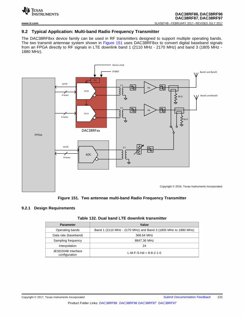
CH B
CH A
FPGA
ADC
2:1
Band1 and Band3
Band1 and Band3
syncb
syncb
4 lanes
4 lanes
8 lanes
Device clock
SYSREF
2:1PA
2:1PA
DAC38RFxx
50 Q�
50 Q�
PLL
Copyright © 2016, Texas Instruments Incorporated
131
DAC38RF86, DAC38RF96DAC38RF87, DAC38RF97
www.ti.com SLASEF4B –FEBRUARY 2017–REVISED JULY 2017
Product Folder Links: DAC38RF86 DAC38RF96 DAC38RF87 DAC38RF97
Submit Documentation FeedbackCopyright © 2017, Texas Instruments Incorporated
9.2 Typical Application: Multi-band Radio Frequency TransmitterThe DAC38RF8xx device family can be used in RF transmitters designed to support multiple operating bands.The two transmit antennae system shown in Figure 151 uses DAC38RF8xx to convert digital baseband signalsfrom an FPGA directly to RF signals in LTE downlink band 1 (2110 MHz - 2170 MHz) and band 3 (1805 MHz -1880 MHz).
Figure 151. Two antennae multi-band Radio Frequency Transmitter
9.2.1 Design Requirements
Table 132. Dual band LTE downlink transmitterParameter Value
Operating bands Band 1 (2110 MHz - 2170 MHz) and Band 3 (1805 MHz to 1880 MHz)Data rate (baseband) 368.64 MHzSampling frequency 8847.36 MHz
Interpolation 24JESD204B Interface
configuration L-M-F-S-Hd = 8-8-2-1-0
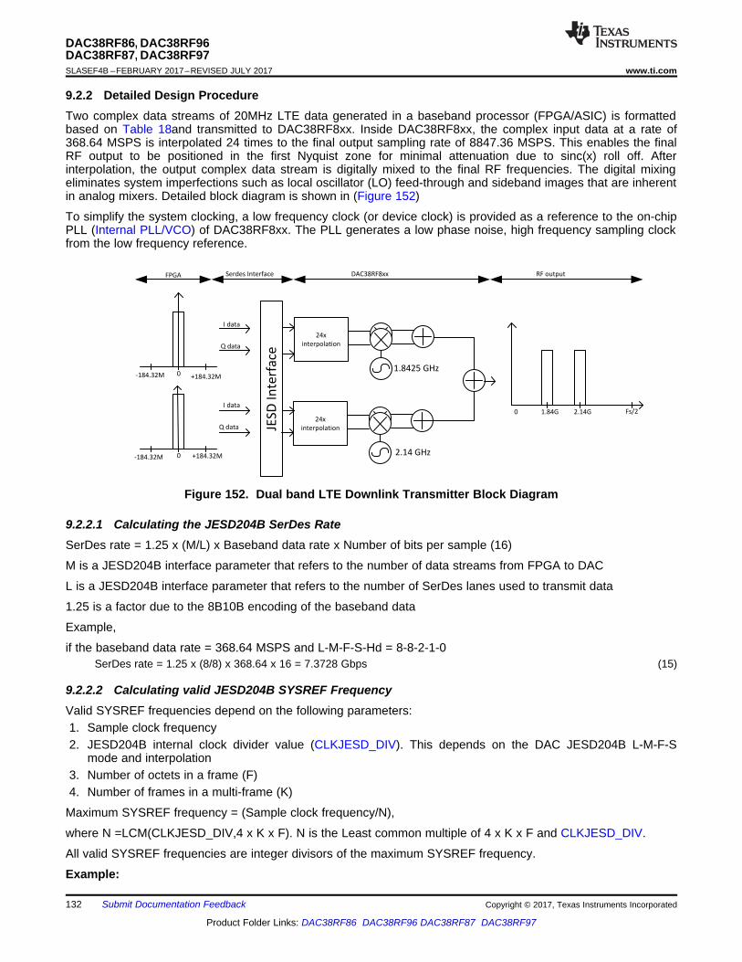
24x
interpolation
JES
D I
nte
rfa
ce
1.8425 GHz
24x
interpolation
2.14 GHz
I data
Q data
I data
Q data
0-184.32M
+184.32M0-184.32M
+184.32M
1.84G 2.14G0
FPGA Serdes Interface DAC38RF8xx RF output
Fs/2
132
DAC38RF86, DAC38RF96DAC38RF87, DAC38RF97SLASEF4B –FEBRUARY 2017–REVISED JULY 2017 www.ti.com
Product Folder Links: DAC38RF86 DAC38RF96 DAC38RF87 DAC38RF97
Submit Documentation Feedback Copyright © 2017, Texas Instruments Incorporated
9.2.2 Detailed Design ProcedureTwo complex data streams of 20MHz LTE data generated in a baseband processor (FPGA/ASIC) is formattedbased on Table 18and transmitted to DAC38RF8xx. Inside DAC38RF8xx, the complex input data at a rate of368.64 MSPS is interpolated 24 times to the final output sampling rate of 8847.36 MSPS. This enables the finalRF output to be positioned in the first Nyquist zone for minimal attenuation due to sinc(x) roll off. Afterinterpolation, the output complex data stream is digitally mixed to the final RF frequencies. The digital mixingeliminates system imperfections such as local oscillator (LO) feed-through and sideband images that are inherentin analog mixers. Detailed block diagram is shown in (Figure 152)
To simplify the system clocking, a low frequency clock (or device clock) is provided as a reference to the on-chipPLL (Internal PLL/VCO) of DAC38RF8xx. The PLL generates a low phase noise, high frequency sampling clockfrom the low frequency reference.
Figure 152. Dual band LTE Downlink Transmitter Block Diagram
9.2.2.1 Calculating the JESD204B SerDes RateSerDes rate = 1.25 x (M/L) x Baseband data rate x Number of bits per sample (16)
M is a JESD204B interface parameter that refers to the number of data streams from FPGA to DAC
L is a JESD204B interface parameter that refers to the number of SerDes lanes used to transmit data
1.25 is a factor due to the 8B10B encoding of the baseband data
Example,
if the baseband data rate = 368.64 MSPS and L-M-F-S-Hd = 8-8-2-1-0SerDes rate = 1.25 x (8/8) x 368.64 x 16 = 7.3728 Gbps (15)
9.2.2.2 Calculating valid JESD204B SYSREF FrequencyValid SYSREF frequencies depend on the following parameters:1. Sample clock frequency2. JESD204B internal clock divider value (CLKJESD_DIV). This depends on the DAC JESD204B L-M-F-S
mode and interpolation3. Number of octets in a frame (F)4. Number of frames in a multi-frame (K)
Maximum SYSREF frequency = (Sample clock frequency/N),
where N =LCM(CLKJESD_DIV,4 x K x F). N is the Least common multiple of 4 x K x F and CLKJESD_DIV.
All valid SYSREF frequencies are integer divisors of the maximum SYSREF frequency.
Example:

133
DAC38RF86, DAC38RF96DAC38RF87, DAC38RF97
www.ti.com SLASEF4B –FEBRUARY 2017–REVISED JULY 2017
Product Folder Links: DAC38RF86 DAC38RF96 DAC38RF87 DAC38RF97
Submit Documentation FeedbackCopyright © 2017, Texas Instruments Incorporated
Given sampling clock frequency = 8.84736 GSPS, Interpolation = 24, DAC Mode=L-M-F-S=8-8-2-1 and K=20:
CLKJESD_DIV = 24 (CLKJESD_DIV)
Maximum SYSREF Frequency = 8847.36 MHz/240 = 36.864 MHz
Valid SYSREF Frequencies = 36.864 MHz/n, where n is any positive integer.
9.2.3 Application Curves
Figure 153. Dual band ACPR Performance in Downlink Band 3 with On-chip PLL
Figure 154. Dual band ACPR Performance in Downlink Band 1 with On-chip PLL
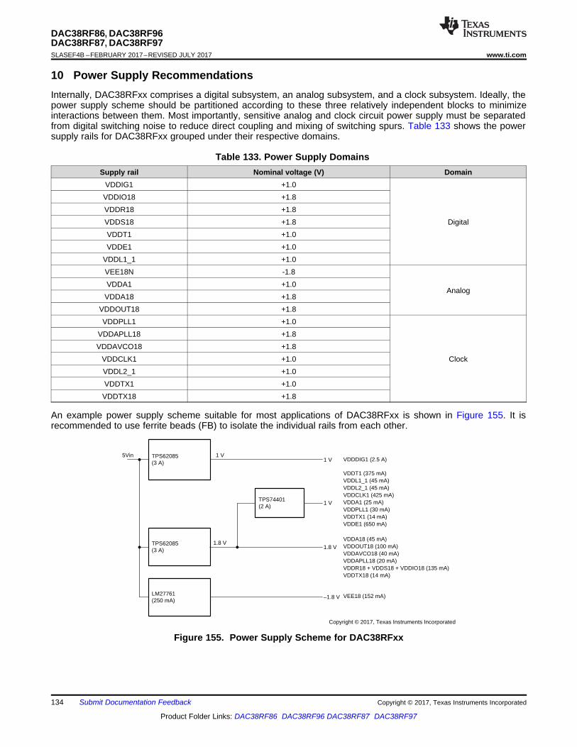
TPS62085(3 A)
5Vin
TPS62085(3 A)
LM27761(250 mA)
1 V1 V
1.8 V
TPS74401(2 A)
1 V
1.8 V
±1.8 V
VDDDIG1 (2.5 A)
VDDT1 (375 mA)VDDL1_1 (45 mA)VDDL2_1 (45 mA)VDDCLK1 (425 mA)VDDA1 (25 mA)VDDPLL1 (30 mA)VDDTX1 (14 mA)VDDE1 (650 mA)
VDDA18 (45 mA)VDDOUT18 (100 mA)VDDAVCO18 (40 mA)VDDAPLL18 (20 mA)VDDR18 + VDDS18 + VDDIO18 (135 mA)VDDTX18 (14 mA)
VEE18 (152 mA)
Copyright © 2017, Texas Instruments Incorporated
134
DAC38RF86, DAC38RF96DAC38RF87, DAC38RF97SLASEF4B –FEBRUARY 2017–REVISED JULY 2017 www.ti.com
Product Folder Links: DAC38RF86 DAC38RF96 DAC38RF87 DAC38RF97
Submit Documentation Feedback Copyright © 2017, Texas Instruments Incorporated
10 Power Supply RecommendationsInternally, DAC38RFxx comprises a digital subsystem, an analog subsystem, and a clock subsystem. Ideally, thepower supply scheme should be partitioned according to these three relatively independent blocks to minimizeinteractions between them. Most importantly, sensitive analog and clock circuit power supply must be separatedfrom digital switching noise to reduce direct coupling and mixing of switching spurs. Table 133 shows the powersupply rails for DAC38RFxx grouped under their respective domains.
Table 133. Power Supply DomainsSupply rail Nominal voltage (V) Domain
VDDIG1 +1.0
Digital
VDDIO18 +1.8VDDR18 +1.8VDDS18 +1.8VDDT1 +1.0VDDE1 +1.0
VDDL1_1 +1.0VEE18N -1.8
AnalogVDDA1 +1.0
VDDA18 +1.8VDDOUT18 +1.8VDDPLL1 +1.0
Clock
VDDAPLL18 +1.8VDDAVCO18 +1.8
VDDCLK1 +1.0VDDL2_1 +1.0VDDTX1 +1.0VDDTX18 +1.8
An example power supply scheme suitable for most applications of DAC38RFxx is shown in Figure 155. It isrecommended to use ferrite beads (FB) to isolate the individual rails from each other.
Figure 155. Power Supply Scheme for DAC38RFxx
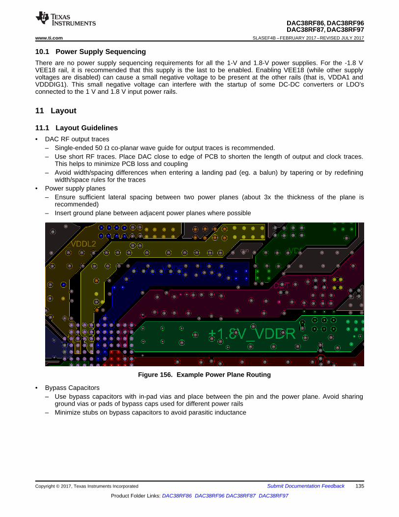
135
DAC38RF86, DAC38RF96DAC38RF87, DAC38RF97
www.ti.com SLASEF4B –FEBRUARY 2017–REVISED JULY 2017
Product Folder Links: DAC38RF86 DAC38RF96 DAC38RF87 DAC38RF97
Submit Documentation FeedbackCopyright © 2017, Texas Instruments Incorporated
10.1 Power Supply SequencingThere are no power supply sequencing requirements for all the 1-V and 1.8-V power supplies. For the -1.8 VVEE18 rail, it is recommended that this supply is the last to be enabled. Enabling VEE18 (while other supplyvoltages are disabled) can cause a small negative voltage to be present at the other rails (that is, VDDA1 andVDDDIG1). This small negative voltage can interfere with the startup of some DC-DC converters or LDO'sconnected to the 1 V and 1.8 V input power rails.
11 Layout
11.1 Layout Guidelines• DAC RF output traces
– Single-ended 50 Ω co-planar wave guide for output traces is recommended.– Use short RF traces. Place DAC close to edge of PCB to shorten the length of output and clock traces.
This helps to minimize PCB loss and coupling– Avoid width/spacing differences when entering a landing pad (eg. a balun) by tapering or by redefining
width/space rules for the traces• Power supply planes
– Ensure sufficient lateral spacing between two power planes (about 3x the thickness of the plane isrecommended)
– Insert ground plane between adjacent power planes where possible
Figure 156. Example Power Plane Routing
• Bypass Capacitors– Use bypass capacitors with in-pad vias and place between the pin and the power plane. Avoid sharing
ground vias or pads of bypass caps used for different power rails– Minimize stubs on bypass capacitors to avoid parasitic inductance
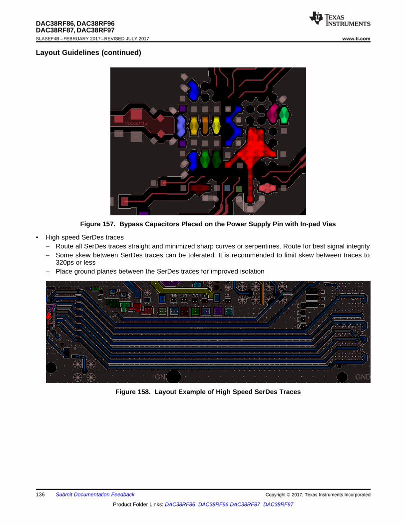
136
DAC38RF86, DAC38RF96DAC38RF87, DAC38RF97SLASEF4B –FEBRUARY 2017–REVISED JULY 2017 www.ti.com
Product Folder Links: DAC38RF86 DAC38RF96 DAC38RF87 DAC38RF97
Submit Documentation Feedback Copyright © 2017, Texas Instruments Incorporated
Layout Guidelines (continued)
Figure 157. Bypass Capacitors Placed on the Power Supply Pin with In-pad Vias
• High speed SerDes traces– Route all SerDes traces straight and minimized sharp curves or serpentines. Route for best signal integrity– Some skew between SerDes traces can be tolerated. It is recommended to limit skew between traces to
320ps or less– Place ground planes between the SerDes traces for improved isolation
Figure 158. Layout Example of High Speed SerDes Traces
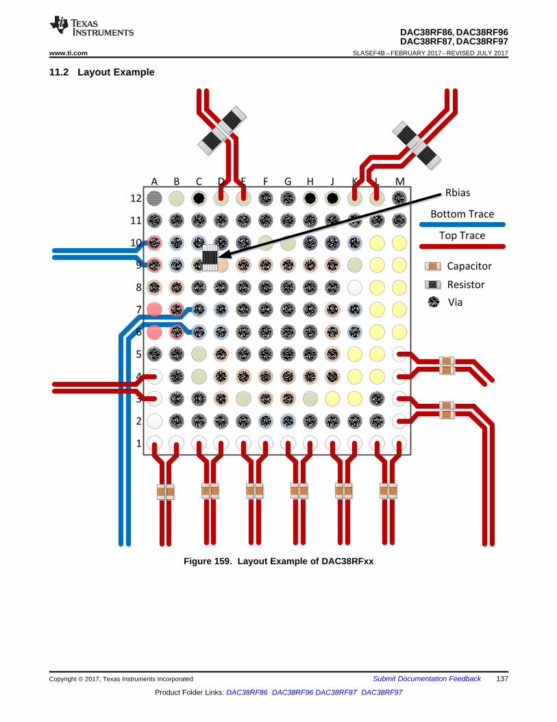
A B C D E F G H J K L M
12
11
10
9
8
5
4
3
2
1
xxxxxxxx
xx
xx
xxxxxxxxxxxxxx
xx
xx
xx
xxxxxxx
7
6xxxx
xxxx
xxxx
xxx x x xxx x x
xxxxxxxxxxxxxxxxxxxxxxxxxxxx
x x xxxxxxxx
xxxxxxxx
xxxx
xxxx
xx
xx
xxxx
xx
xxxxx
xxxxxxx
xx
xx
xx
xxxxxxxxxxxxx
xxxxxxxxxxxxxxx
xx
xxxx
xxxx
xxxxxx
xxxxxxxxxxxxxx
xx
x xx x
Bottom Trace
Top Trace
Capacitor
Resistor
xx
Via
Rbias
x xxx
137
DAC38RF86, DAC38RF96DAC38RF87, DAC38RF97
www.ti.com SLASEF4B –FEBRUARY 2017–REVISED JULY 2017
Product Folder Links: DAC38RF86 DAC38RF96 DAC38RF87 DAC38RF97
Submit Documentation FeedbackCopyright © 2017, Texas Instruments Incorporated
11.2 Layout Example
Figure 159. Layout Example of DAC38RFxx
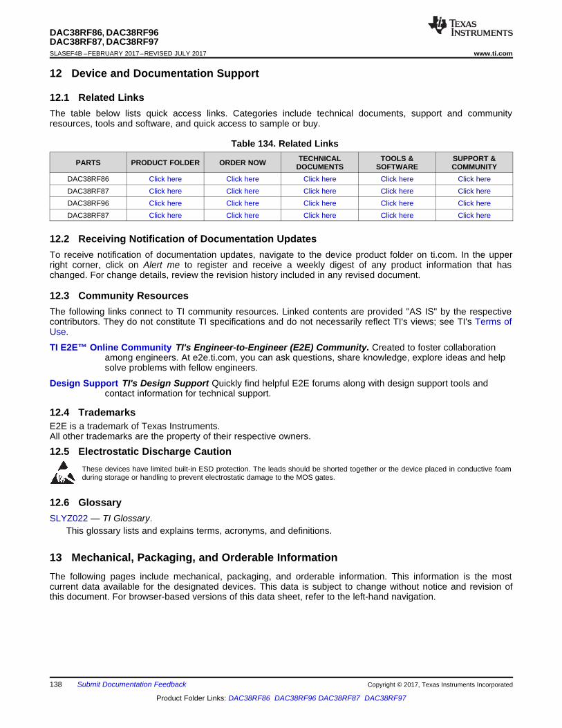
138
DAC38RF86, DAC38RF96DAC38RF87, DAC38RF97SLASEF4B –FEBRUARY 2017–REVISED JULY 2017 www.ti.com
Product Folder Links: DAC38RF86 DAC38RF96 DAC38RF87 DAC38RF97
Submit Documentation Feedback Copyright © 2017, Texas Instruments Incorporated
12 Device and Documentation Support
12.1 Related LinksThe table below lists quick access links. Categories include technical documents, support and communityresources, tools and software, and quick access to sample or buy.
Table 134. Related Links
PARTS PRODUCT FOLDER ORDER NOW TECHNICALDOCUMENTS
TOOLS &SOFTWARE
SUPPORT &COMMUNITY
DAC38RF86 Click here Click here Click here Click here Click hereDAC38RF87 Click here Click here Click here Click here Click hereDAC38RF96 Click here Click here Click here Click here Click hereDAC38RF87 Click here Click here Click here Click here Click here
12.2 Receiving Notification of Documentation UpdatesTo receive notification of documentation updates, navigate to the device product folder on ti.com. In the upperright corner, click on Alert me to register and receive a weekly digest of any product information that haschanged. For change details, review the revision history included in any revised document.
12.3 Community ResourcesThe following links connect to TI community resources. Linked contents are provided "AS IS" by the respectivecontributors. They do not constitute TI specifications and do not necessarily reflect TI's views; see TI's Terms ofUse.
TI E2E™ Online Community TI's Engineer-to-Engineer (E2E) Community. Created to foster collaborationamong engineers. At e2e.ti.com, you can ask questions, share knowledge, explore ideas and helpsolve problems with fellow engineers.
Design Support TI's Design Support Quickly find helpful E2E forums along with design support tools andcontact information for technical support.
12.4 TrademarksE2E is a trademark of Texas Instruments.All other trademarks are the property of their respective owners.
12.5 Electrostatic Discharge CautionThese devices have limited built-in ESD protection. The leads should be shorted together or the device placed in conductive foamduring storage or handling to prevent electrostatic damage to the MOS gates.
12.6 GlossarySLYZ022 — TI Glossary.
This glossary lists and explains terms, acronyms, and definitions.
13 Mechanical, Packaging, and Orderable InformationThe following pages include mechanical, packaging, and orderable information. This information is the mostcurrent data available for the designated devices. This data is subject to change without notice and revision ofthis document. For browser-based versions of this data sheet, refer to the left-hand navigation.
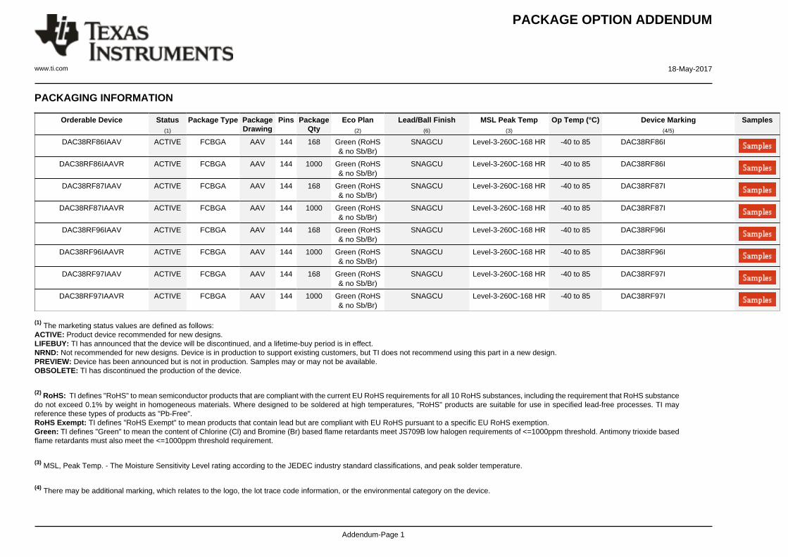
PACKAGE OPTION ADDENDUM
www.ti.com 18-May-2017
Addendum-Page 1
PACKAGING INFORMATION
Orderable Device Status(1)
Package Type PackageDrawing
Pins PackageQty
Eco Plan(2)
Lead/Ball Finish(6)
MSL Peak Temp(3)
Op Temp (°C) Device Marking(4/5)
Samples
DAC38RF86IAAV ACTIVE FCBGA AAV 144 168 Green (RoHS& no Sb/Br)
SNAGCU Level-3-260C-168 HR -40 to 85 DAC38RF86I
DAC38RF86IAAVR ACTIVE FCBGA AAV 144 1000 Green (RoHS& no Sb/Br)
SNAGCU Level-3-260C-168 HR -40 to 85 DAC38RF86I
DAC38RF87IAAV ACTIVE FCBGA AAV 144 168 Green (RoHS& no Sb/Br)
SNAGCU Level-3-260C-168 HR -40 to 85 DAC38RF87I
DAC38RF87IAAVR ACTIVE FCBGA AAV 144 1000 Green (RoHS& no Sb/Br)
SNAGCU Level-3-260C-168 HR -40 to 85 DAC38RF87I
DAC38RF96IAAV ACTIVE FCBGA AAV 144 168 Green (RoHS& no Sb/Br)
SNAGCU Level-3-260C-168 HR -40 to 85 DAC38RF96I
DAC38RF96IAAVR ACTIVE FCBGA AAV 144 1000 Green (RoHS& no Sb/Br)
SNAGCU Level-3-260C-168 HR -40 to 85 DAC38RF96I
DAC38RF97IAAV ACTIVE FCBGA AAV 144 168 Green (RoHS& no Sb/Br)
SNAGCU Level-3-260C-168 HR -40 to 85 DAC38RF97I
DAC38RF97IAAVR ACTIVE FCBGA AAV 144 1000 Green (RoHS& no Sb/Br)
SNAGCU Level-3-260C-168 HR -40 to 85 DAC38RF97I
(1) The marketing status values are defined as follows:ACTIVE: Product device recommended for new designs.LIFEBUY: TI has announced that the device will be discontinued, and a lifetime-buy period is in effect.NRND: Not recommended for new designs. Device is in production to support existing customers, but TI does not recommend using this part in a new design.PREVIEW: Device has been announced but is not in production. Samples may or may not be available.OBSOLETE: TI has discontinued the production of the device.
(2) RoHS: TI defines "RoHS" to mean semiconductor products that are compliant with the current EU RoHS requirements for all 10 RoHS substances, including the requirement that RoHS substancedo not exceed 0.1% by weight in homogeneous materials. Where designed to be soldered at high temperatures, "RoHS" products are suitable for use in specified lead-free processes. TI mayreference these types of products as "Pb-Free".RoHS Exempt: TI defines "RoHS Exempt" to mean products that contain lead but are compliant with EU RoHS pursuant to a specific EU RoHS exemption.Green: TI defines "Green" to mean the content of Chlorine (Cl) and Bromine (Br) based flame retardants meet JS709B low halogen requirements of <=1000ppm threshold. Antimony trioxide basedflame retardants must also meet the <=1000ppm threshold requirement.
(3) MSL, Peak Temp. - The Moisture Sensitivity Level rating according to the JEDEC industry standard classifications, and peak solder temperature.
(4) There may be additional marking, which relates to the logo, the lot trace code information, or the environmental category on the device.
PACKAGE OPTION ADDENDUM
www.ti.com 18-May-2017
Addendum-Page 2
(5) Multiple Device Markings will be inside parentheses. Only one Device Marking contained in parentheses and separated by a "~" will appear on a device. If a line is indented then it is a continuationof the previous line and the two combined represent the entire Device Marking for that device.
(6) Lead/Ball Finish - Orderable Devices may have multiple material finish options. Finish options are separated by a vertical ruled line. Lead/Ball Finish values may wrap to two lines if the finishvalue exceeds the maximum column width.
Important Information and Disclaimer:The information provided on this page represents TI's knowledge and belief as of the date that it is provided. TI bases its knowledge and belief on informationprovided by third parties, and makes no representation or warranty as to the accuracy of such information. Efforts are underway to better integrate information from third parties. TI has taken andcontinues to take reasonable steps to provide representative and accurate information but may not have conducted destructive testing or chemical analysis on incoming materials and chemicals.TI and TI suppliers consider certain information to be proprietary, and thus CAS numbers and other limited information may not be available for release.
In no event shall TI's liability arising out of such information exceed the total purchase price of the TI part(s) at issue in this document sold by TI to Customer on an annual basis.
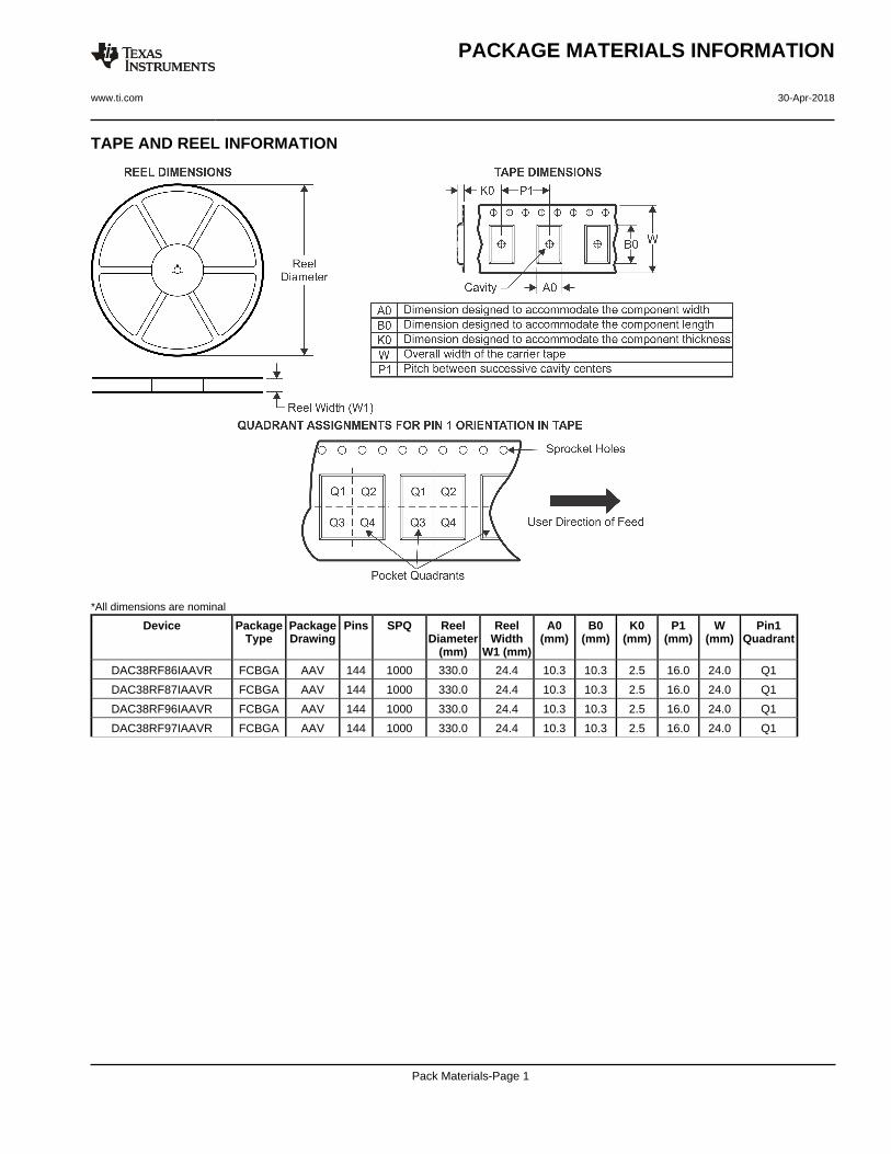
TAPE AND REEL INFORMATION
*All dimensions are nominal
Device PackageType
PackageDrawing
Pins SPQ ReelDiameter
(mm)
ReelWidth
W1 (mm)
A0(mm)
B0(mm)
K0(mm)
P1(mm)
W(mm)
Pin1Quadrant
DAC38RF86IAAVR FCBGA AAV 144 1000 330.0 24.4 10.3 10.3 2.5 16.0 24.0 Q1
DAC38RF87IAAVR FCBGA AAV 144 1000 330.0 24.4 10.3 10.3 2.5 16.0 24.0 Q1
DAC38RF96IAAVR FCBGA AAV 144 1000 330.0 24.4 10.3 10.3 2.5 16.0 24.0 Q1
DAC38RF97IAAVR FCBGA AAV 144 1000 330.0 24.4 10.3 10.3 2.5 16.0 24.0 Q1
PACKAGE MATERIALS INFORMATION
www.ti.com 30-Apr-2018
Pack Materials-Page 1
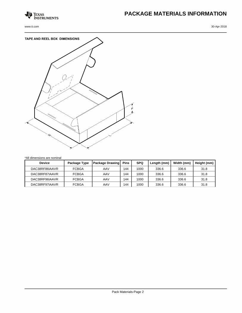
*All dimensions are nominal
Device Package Type Package Drawing Pins SPQ Length (mm) Width (mm) Height (mm)
DAC38RF86IAAVR FCBGA AAV 144 1000 336.6 336.6 31.8
DAC38RF87IAAVR FCBGA AAV 144 1000 336.6 336.6 31.8
DAC38RF96IAAVR FCBGA AAV 144 1000 336.6 336.6 31.8
DAC38RF97IAAVR FCBGA AAV 144 1000 336.6 336.6 31.8
PACKAGE MATERIALS INFORMATION
www.ti.com 30-Apr-2018
Pack Materials-Page 2
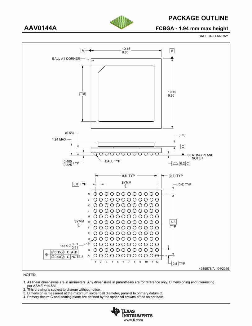
www.ti.com
PACKAGE OUTLINE
C
1.94 MAX
TYP0.4050.325
8.8TYP
8.8 TYP
0.8 TYP
0.8 TYP
144X 0.510.41
(0.68)
A 10.159.85 B
10.159.85
(0.6) TYP
( 8)
(0.5)
(0.6) TYP
FCBGA - 1.94 mm max heightAAV0144ABALL GRID ARRAY
4219578/A 04/2016
NOTES: 1. All linear dimensions are in millimeters. Any dimensions in parenthesis are for reference only. Dimensioning and tolerancing per ASME Y14.5M. 2. This drawing is subject to change without notice.3. Dimension is measured at the maximum solder ball diameter, parallel to primary datum C.4. Primary datum C and seating plane are defined by the spherical crowns of the solder balls.
BALL A1 CORNER
SEATING PLANE
BALL TYP0.2 C
NOTE 4
M
L
K
J
H
G
F
E
D
C
B
A
1 2 3
0.15 C A B0.08 C
SYMM
SYMM
4
NOTE 35 6 7 8 9 10 11 12
SCALE 1.400

www.ti.com
EXAMPLE BOARD LAYOUT
144X ( )0.4
(0.8) TYP
(0.8) TYP
( )METAL
0.4 0.05 MAX
SOLDER MASKOPENING
METAL UNDERSOLDER MASK
( )SOLDER MASKOPENING
0.4
0.05 MIN
FCBGA - 1.94 mm max heightAAV0144ABALL GRID ARRAY
4219578/A 04/2016
NOTES: (continued) 5. Final dimensions may vary due to manufacturing tolerance considerations and also routing constraints. For more information, see Texas Instruments literature number SPRU811 (www.ti.com/lit/spru811).
SYMM
SYMM
LAND PATTERN EXAMPLESCALE:8X
1A
B
C
D
E
F
G
H
J
K
L
M
2 3 4 5 6 7 8 9 10 11 12
NON-SOLDER MASKDEFINED
(PREFERRED)
SOLDER MASK DETAILSNOT TO SCALE
SOLDER MASKDEFINED

www.ti.com
EXAMPLE STENCIL DESIGN
(0.8)TYP
(0.8) TYP 144X ( )0.4
FCBGA - 1.94 mm max heightAAV0144ABALL GRID ARRAY
4219578/A 04/2016
NOTES: (continued) 6. Laser cutting apertures with trapezoidal walls and rounded corners may offer better paste release.
SOLDER PASTE EXAMPLEBASED ON 0.15 mm THICK STENCIL
SCALE:8X
SYMM
SYMM
1A
B
C
D
E
F
G
H
J
K
L
M
2 3 4 5 6 7 8 9 10 11 12

IMPORTANT NOTICE
Texas Instruments Incorporated (TI) reserves the right to make corrections, enhancements, improvements and other changes to itssemiconductor products and services per JESD46, latest issue, and to discontinue any product or service per JESD48, latest issue. Buyersshould obtain the latest relevant information before placing orders and should verify that such information is current and complete.TI’s published terms of sale for semiconductor products (http://www.ti.com/sc/docs/stdterms.htm) apply to the sale of packaged integratedcircuit products that TI has qualified and released to market. Additional terms may apply to the use or sale of other types of TI products andservices.Reproduction of significant portions of TI information in TI data sheets is permissible only if reproduction is without alteration and isaccompanied by all associated warranties, conditions, limitations, and notices. TI is not responsible or liable for such reproduceddocumentation. Information of third parties may be subject to additional restrictions. Resale of TI products or services with statementsdifferent from or beyond the parameters stated by TI for that product or service voids all express and any implied warranties for theassociated TI product or service and is an unfair and deceptive business practice. TI is not responsible or liable for any such statements.Buyers and others who are developing systems that incorporate TI products (collectively, “Designers”) understand and agree that Designersremain responsible for using their independent analysis, evaluation and judgment in designing their applications and that Designers havefull and exclusive responsibility to assure the safety of Designers' applications and compliance of their applications (and of all TI productsused in or for Designers’ applications) with all applicable regulations, laws and other applicable requirements. Designer represents that, withrespect to their applications, Designer has all the necessary expertise to create and implement safeguards that (1) anticipate dangerousconsequences of failures, (2) monitor failures and their consequences, and (3) lessen the likelihood of failures that might cause harm andtake appropriate actions. Designer agrees that prior to using or distributing any applications that include TI products, Designer willthoroughly test such applications and the functionality of such TI products as used in such applications.TI’s provision of technical, application or other design advice, quality characterization, reliability data or other services or information,including, but not limited to, reference designs and materials relating to evaluation modules, (collectively, “TI Resources”) are intended toassist designers who are developing applications that incorporate TI products; by downloading, accessing or using TI Resources in anyway, Designer (individually or, if Designer is acting on behalf of a company, Designer’s company) agrees to use any particular TI Resourcesolely for this purpose and subject to the terms of this Notice.TI’s provision of TI Resources does not expand or otherwise alter TI’s applicable published warranties or warranty disclaimers for TIproducts, and no additional obligations or liabilities arise from TI providing such TI Resources. TI reserves the right to make corrections,enhancements, improvements and other changes to its TI Resources. TI has not conducted any testing other than that specificallydescribed in the published documentation for a particular TI Resource.Designer is authorized to use, copy and modify any individual TI Resource only in connection with the development of applications thatinclude the TI product(s) identified in such TI Resource. NO OTHER LICENSE, EXPRESS OR IMPLIED, BY ESTOPPEL OR OTHERWISETO ANY OTHER TI INTELLECTUAL PROPERTY RIGHT, AND NO LICENSE TO ANY TECHNOLOGY OR INTELLECTUAL PROPERTYRIGHT OF TI OR ANY THIRD PARTY IS GRANTED HEREIN, including but not limited to any patent right, copyright, mask work right, orother intellectual property right relating to any combination, machine, or process in which TI products or services are used. Informationregarding or referencing third-party products or services does not constitute a license to use such products or services, or a warranty orendorsement thereof. Use of TI Resources may require a license from a third party under the patents or other intellectual property of thethird party, or a license from TI under the patents or other intellectual property of TI.TI RESOURCES ARE PROVIDED “AS IS” AND WITH ALL FAULTS. TI DISCLAIMS ALL OTHER WARRANTIES ORREPRESENTATIONS, EXPRESS OR IMPLIED, REGARDING RESOURCES OR USE THEREOF, INCLUDING BUT NOT LIMITED TOACCURACY OR COMPLETENESS, TITLE, ANY EPIDEMIC FAILURE WARRANTY AND ANY IMPLIED WARRANTIES OFMERCHANTABILITY, FITNESS FOR A PARTICULAR PURPOSE, AND NON-INFRINGEMENT OF ANY THIRD PARTY INTELLECTUALPROPERTY RIGHTS. TI SHALL NOT BE LIABLE FOR AND SHALL NOT DEFEND OR INDEMNIFY DESIGNER AGAINST ANY CLAIM,INCLUDING BUT NOT LIMITED TO ANY INFRINGEMENT CLAIM THAT RELATES TO OR IS BASED ON ANY COMBINATION OFPRODUCTS EVEN IF DESCRIBED IN TI RESOURCES OR OTHERWISE. IN NO EVENT SHALL TI BE LIABLE FOR ANY ACTUAL,DIRECT, SPECIAL, COLLATERAL, INDIRECT, PUNITIVE, INCIDENTAL, CONSEQUENTIAL OR EXEMPLARY DAMAGES INCONNECTION WITH OR ARISING OUT OF TI RESOURCES OR USE THEREOF, AND REGARDLESS OF WHETHER TI HAS BEENADVISED OF THE POSSIBILITY OF SUCH DAMAGES.Unless TI has explicitly designated an individual product as meeting the requirements of a particular industry standard (e.g., ISO/TS 16949and ISO 26262), TI is not responsible for any failure to meet such industry standard requirements.Where TI specifically promotes products as facilitating functional safety or as compliant with industry functional safety standards, suchproducts are intended to help enable customers to design and create their own applications that meet applicable functional safety standardsand requirements. Using products in an application does not by itself establish any safety features in the application. Designers mustensure compliance with safety-related requirements and standards applicable to their applications. Designer may not use any TI products inlife-critical medical equipment unless authorized officers of the parties have executed a special contract specifically governing such use.Life-critical medical equipment is medical equipment where failure of such equipment would cause serious bodily injury or death (e.g., lifesupport, pacemakers, defibrillators, heart pumps, neurostimulators, and implantables). Such equipment includes, without limitation, allmedical devices identified by the U.S. Food and Drug Administration as Class III devices and equivalent classifications outside the U.S.TI may expressly designate certain products as completing a particular qualification (e.g., Q100, Military Grade, or Enhanced Product).Designers agree that it has the necessary expertise to select the product with the appropriate qualification designation for their applicationsand that proper product selection is at Designers’ own risk. Designers are solely responsible for compliance with all legal and regulatoryrequirements in connection with such selection.Designer will fully indemnify TI and its representatives against any damages, costs, losses, and/or liabilities arising out of Designer’s non-compliance with the terms and provisions of this Notice.
Mailing Address: Texas Instruments, Post Office Box 655303, Dallas, Texas 75265Copyright © 2018, Texas Instruments Incorporated