Embed Size (px)
Citation preview
ECCN 5E002 TSPA - Technology / Software Publicly Available
ErrataSLAZ052E–May 2009–Revised January 2011
CC430F613x, 'F612x, 'F513x Device Erratasheet
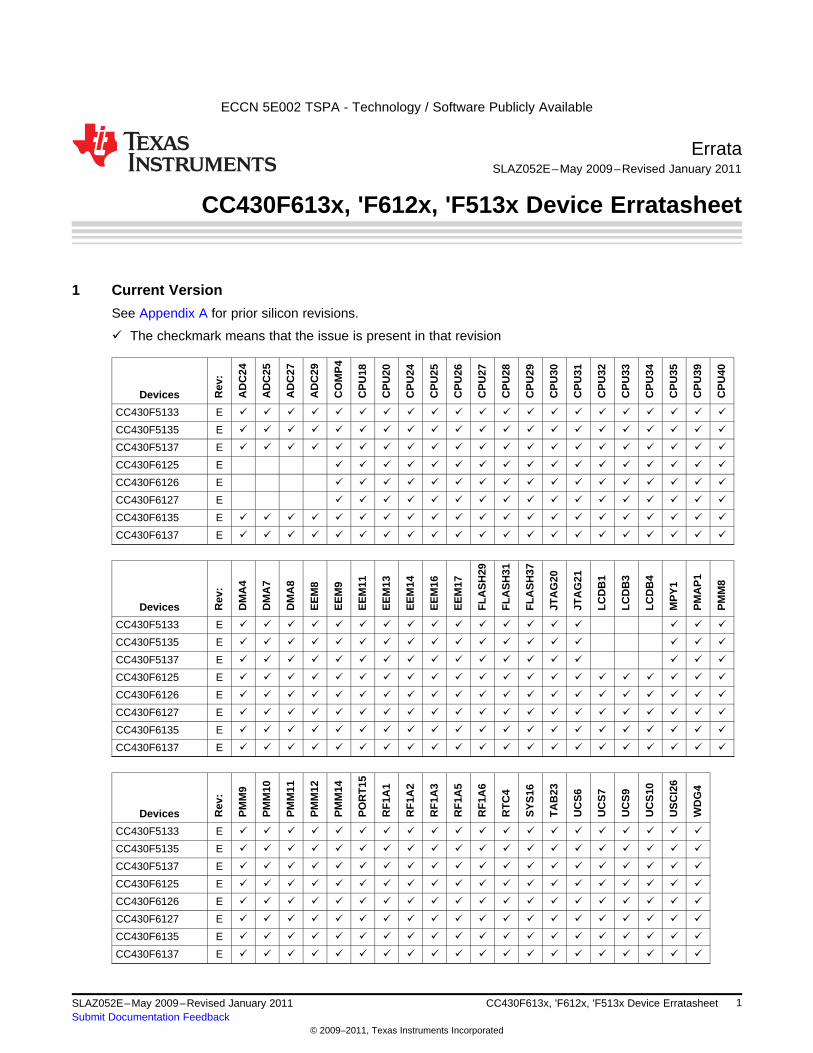
1 Current Version
See Appendix A for prior silicon revisions.
ü The checkmark means that the issue is present in that revision
Devices Rev
:
AD
C24
AD
C25
AD
C27
AD
C29
CO
MP
4
CP
U18
CP
U20
CP
U24
CP
U25
CP
U26
CP
U27
CP
U28
CP
U29
CP
U30
CP
U31
CP
U32
CP
U33
CP
U34
CP
U35
CP
U39
CP
U40
CC430F5133 E ü ü ü ü ü ü ü ü ü ü ü ü ü ü ü ü ü ü ü ü ü
CC430F5135 E ü ü ü ü ü ü ü ü ü ü ü ü ü ü ü ü ü ü ü ü ü
CC430F5137 E ü ü ü ü ü ü ü ü ü ü ü ü ü ü ü ü ü ü ü ü ü
CC430F6125 E ü ü ü ü ü ü ü ü ü ü ü ü ü ü ü ü ü
CC430F6126 E ü ü ü ü ü ü ü ü ü ü ü ü ü ü ü ü ü
CC430F6127 E ü ü ü ü ü ü ü ü ü ü ü ü ü ü ü ü ü
CC430F6135 E ü ü ü ü ü ü ü ü ü ü ü ü ü ü ü ü ü ü ü ü ü
CC430F6137 E ü ü ü ü ü ü ü ü ü ü ü ü ü ü ü ü ü ü ü ü ü
Devices Rev
:
DM
A4
DM
A7
DM
A8
EE
M8
EE
M9
EE
M11
EE
M13
EE
M14
EE
M16
EE
M17
FL
AS
H29
FL
AS
H31
FL
AS
H37
JTA
G20
JTA
G21
LC
DB
1
LC
DB
3
LC
DB
4
MP
Y1
PM
AP
1
PM
M8
CC430F5133 E ü ü ü ü ü ü ü ü ü ü ü ü ü ü ü ü ü ü
CC430F5135 E ü ü ü ü ü ü ü ü ü ü ü ü ü ü ü ü ü ü
CC430F5137 E ü ü ü ü ü ü ü ü ü ü ü ü ü ü ü ü ü ü
CC430F6125 E ü ü ü ü ü ü ü ü ü ü ü ü ü ü ü ü ü ü ü ü ü
CC430F6126 E ü ü ü ü ü ü ü ü ü ü ü ü ü ü ü ü ü ü ü ü ü
CC430F6127 E ü ü ü ü ü ü ü ü ü ü ü ü ü ü ü ü ü ü ü ü ü
CC430F6135 E ü ü ü ü ü ü ü ü ü ü ü ü ü ü ü ü ü ü ü ü ü
CC430F6137 E ü ü ü ü ü ü ü ü ü ü ü ü ü ü ü ü ü ü ü ü ü
Devices Rev
:
PM
M9
PM
M10
PM
M11
PM
M12
PM
M14
PO
RT
15
RF
1A1
RF
1A2
RF
1A3
RF
1A5
RF
1A6
RT
C4
SY
S16
TA
B23
UC
S6
UC
S7
UC
S9
UC
S10
US
CI2
6
WD
G4
CC430F5133 E ü ü ü ü ü ü ü ü ü ü ü ü ü ü ü ü ü ü ü ü
CC430F5135 E ü ü ü ü ü ü ü ü ü ü ü ü ü ü ü ü ü ü ü ü
CC430F5137 E ü ü ü ü ü ü ü ü ü ü ü ü ü ü ü ü ü ü ü ü
CC430F6125 E ü ü ü ü ü ü ü ü ü ü ü ü ü ü ü ü ü ü ü ü
CC430F6126 E ü ü ü ü ü ü ü ü ü ü ü ü ü ü ü ü ü ü ü ü
CC430F6127 E ü ü ü ü ü ü ü ü ü ü ü ü ü ü ü ü ü ü ü ü
CC430F6135 E ü ü ü ü ü ü ü ü ü ü ü ü ü ü ü ü ü ü ü ü
CC430F6137 E ü ü ü ü ü ü ü ü ü ü ü ü ü ü ü ü ü ü ü ü
1SLAZ052E–May 2009–Revised January 2011 CC430F613x, 'F612x, 'F513x Device ErratasheetSubmit Documentation Feedback
© 2009–2011, Texas Instruments Incorporated
ECCN 5E002 TSPA - Technology / Software Publicly Available
Package Markings www.ti.com
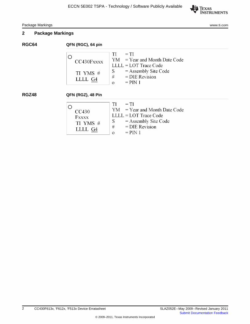
2 Package Markings
RGC64 QFN (RGC), 64 pin
RGZ48 QFN (RGZ), 48 Pin
2 CC430F613x, 'F612x, 'F513x Device Erratasheet SLAZ052E–May 2009–Revised January 2011Submit Documentation Feedback
© 2009–2011, Texas Instruments Incorporated
ECCN 5E002 TSPA - Technology / Software Publicly Available
www.ti.com Detailed Bug Description
3 Detailed Bug Description
ADC24 ADC12 Module
Function Unexpected ADC12 current draw when ADC12ENC = 1
Description When set, the ADC12ENC bit issues a clock request to the selected source clock, evenbefore the conversion trigger. This causes some extra current consumption, dependingon the selected clock.
Workaround None
ADC25 ADC12 Module
Function Write to ADC12CTL0 triggers ADC12 when CONSEQ = 00
Description If ADC conversions are triggered by the Timer_B module and the ADC12 is insingle-channel single-conversion mode (CONSEQ = 00), ADC sampling is enabled bywrite access to any bit(s) in the ADC12CTL0 register. This is contrary to the expectedbehavior that only the ADC12 enable conversion bit (ADC12ENC) triggers a new ADC12sample.
Workaround When operating the ADC12 in CONSEQ = 00 and a Timer_B output is selected as thesample and hold source, temporarily clear the ADC12ENC bit before writing to other bitsin the ADC12CTL0 register. The following capture trigger can then be re-enabled bysetting ADC12ENC = 1.
3SLAZ052E–May 2009–Revised January 2011 CC430F613x, 'F612x, 'F513x Device ErratasheetSubmit Documentation Feedback
© 2009–2011, Texas Instruments Incorporated
ECCN 5E002 TSPA - Technology / Software Publicly Available
Detailed Bug Description www.ti.com
ADC27 ADC12 Module
Function Integral and differential non-linearity exceed specifications
Description The ADC12_A integral and differential non-linearity may exceed the limits specified inthe data sheet under the following conditions:
• If the internal voltage reference generator is usedand
• If the reference voltage is not buffered off-chipand
• If fADC12CLK > 2.7 MHzorIf the internal voltage reference is selected for 1.5-V output mode.
The non-linearity can be up to tens of LSBs. This is due to the internal reference bufferproviding insufficient drive for the switched capacitor array of the ADC12_A.
Workaround
• Turn on the output of the internal voltage reference to increase the drive strength ofthe reference to the ADC_12 core:
– If REFMSTR bit in REFCTL0 is 0 (allowing Shared REF to be controlled byADC_A reference control bits)
Set ADC12REFON bit in ADC12CTL0 = 1andSet ADC12REFOUT bit in ADC12CTL2 = 1
– If REFMSTR bit in REFCTL0 is 1Set REFON and REFOUT bits in REFCTL0 = 1
or• Ensure fADC12CLK < 2.7 MHz and select the internal voltage reference in 2.5-V output
mode.Depending on the frequency of the source of fADC12CLK (ACLK, MCLK, SMCLK, orMODOSC), select the divider bits accordingly.
– If fADC12CLK = MODOSC (ADC12OSC)ADC12CTL1 |= ADC12DIV_2; // Divide clock by 2
– If fADC12CLK = ACLK/SMCLK/MCLK > 2.7 MHzUse ADC12DIVx and/or ADC12PDIVx bits to reduce the selected clock frequencyto between 0.45 MHz and 2.7 MHz.
And set both REFVSELx bits in REFCTL0 to REFVSEL_3 (select 2.5-V output).
ADC29 ADC12 Module
Function Incorrect temperature sensor calibration data
Description In some devices, the internal temperature sensor calibration data for 0°C are invalid forall VRef conditions. Devices with correct calibration data show a difference of at least 30LSBs between the different VRef conditions. When using incorrect calibration data withthe internal temperature sensor ADC samples, the calculated results can be unreliable.Calibration data for 85°C are not affected.
Workaround Recalibrate the temperature sensor for 30°C at the application level.
4 CC430F613x, 'F612x, 'F513x Device Erratasheet SLAZ052E–May 2009–Revised January 2011Submit Documentation Feedback
© 2009–2011, Texas Instruments Incorporated
ECCN 5E002 TSPA - Technology / Software Publicly Available
www.ti.com Detailed Bug Description
COMP4 Comparator_B Module
Function CBEX and CBOUTPOL bits do not invert comparator I/O
Description Setting the exchange bit, CBEX, does not interchange the comparator inputs. Similarlysetting the output polarity bit, CBOUTPOL, does not invert the output of the comparator.
Workaround To obtain an inverted output from the comparator, invert the input signals to thecomparator using the channel input selector bits, CBIPSEL_x and CBIMSEL_x. Makesure to use a MOV instruction so that the inputs are inverted simultaneously.
CPU18 CPU Module
Function LPM instruction can corrupt PC/SR registers
Description The PC and SR registers have the potential to be corrupted when:
• An instruction using register, absolute, indexed, indirect, indirect auto-increment, orsymbolic mode is used to set the LPM bits (e.g., BIS &xyh, SR).and
• This instruction is followed by a CALL or CALLA instruction.
Upon servicing an interrupt service routine, the program counter (PC) is pushed twiceonto the stack instead of the correct operation where the PC, then the SR registers arepushed onto the stack. This corrupts the SR and possibly the PC on RETI from the ISR.
Workaround Insert a NOP or __no_operation() intrinsic function between the instruction to enterlow-power mode and the CALL or CALLA instruction.
CPU20 CPU Module
Function An unexpected Vacant Memory Access Flag (VMAIFG) can be triggered due to the CPUautoincrement of the MAB+2 outside the range of a valid memory block.
Description The VMAIFG can be triggered under the following conditions:
1. If an interrupt is requested, fetched by the CPU, but lost before execution of theinterrupt service routine.or
2. If a PC-modifying instruction (for example, RET, PUSH, CALL, POP, JMP, BR) isfetched from the last address of a section of memory (Flash or RAM) that is notcontiguous to a higher valid section on the memory map.
Workaround For case 1 – None
For case 2 – If code is affected, edit the linker command file to make the last four bytesof affected memory sections unavailable.
5SLAZ052E–May 2009–Revised January 2011 CC430F613x, 'F612x, 'F513x Device ErratasheetSubmit Documentation Feedback
© 2009–2011, Texas Instruments Incorporated
ECCN 5E002 TSPA - Technology / Software Publicly Available
Detailed Bug Description www.ti.com
CPU24 CPU Module
Function Program counter corruption following entry into low-power mode
Description The program counter is corrupted when an interrupt event occurs in the time between(and including) one cycle before and one cycle after the CPUOFF bit is set in the statusregister. This failure occurs when the BIS instruction is followed by a CALL or CALLAinstruction using the following addressing modes:
BIS &, SRCALLA indir, indir autoinc, regBIS INDEX, SRCALLA indir, indir autoinc, regBIS reg, SRCALLA reg, indir, indir autoinc
NOTE: Due to the instruction emulation, the EINT instruction, as well as the__enable_interrupts() and possibly the __bis_SR_register() intrinsicfunctions are affected.
Workaround Insert a NOP instruction or __no_operation() intrinsic function call between the BIS andCALL or CALLA instructions.
CPU25 CPU Module
Function DMA transfer does not execute during low-power mode
Description If the following instruction sequence is used ([] denotes an addressing mode) to enter alow-power mode, and the DMARMWDIS bit is set, then DMA transfers are blocked forthe duration of the low-power mode.
BIS [register|index|absolute|symbolic],SRCALLA [register]
Workaround
• Insert a NOP instruction or __no_operation() intrinsic function call between the BISand CALLA instructionsor
• Temporarily disable the DMARMWDIS bit when entering low-power mode.
CPU26 CPU Module
Function CALL SP does not behave as expected
Description When the intention is to execute code from the stack, a CALL SP instruction skips thefirst piece of data (instruction) on the stack. The second piece of data at SP + 2 is usedas the first executable instruction.
Workaround Write the op code for a NOP as the first instruction on the stack. Begin the intendedsubroutine at address SP + 2.
6 CC430F613x, 'F612x, 'F513x Device Erratasheet SLAZ052E–May 2009–Revised January 2011Submit Documentation Feedback
© 2009–2011, Texas Instruments Incorporated
ECCN 5E002 TSPA - Technology / Software Publicly Available
www.ti.com Detailed Bug Description
CPU27 CPU Module
Function Program Counter (PC) is corrupted during the context save of a nested interrupt
Description When a low-power mode is entered within an interrupt service routine that has enablednested interrupts (by setting the GIE bit), and the instruction that sets the low-powermode is directly followed by a RETI instruction, an incorrect value of PC + 2 is pushed tothe stack during the context save. Hence, the RETI instruction is not executed on returnfrom the nested interrupt, and the PC becomes corrupted.
Workaround Insert a NOP or __no_operation() intrinsic function between the instruction that sets thelower power mode and the RETI instruction.
CPU28 CPU Module
Function PC is corrupted when using certain extended addressing mode combinations
Description An extended memory instruction that modifies the program counter executes incorrectlywhen preceded by an extended memory write-back instruction under the followingconditions:
First instruction:2-operand instruction, extended mode using (register,index), (register,absolute), or(register,symbolic) addressing modes
Second instruction:2-operand instruction, extended mode using the (indirect,PC), (indirectauto-increment,PC), or (indexed [with ind 0], PC) addressing modes
Example BISX.A R6,&AABCDANDX.A @R4+,PC
Workaround
• Insert a NOP or a __no_operation() intrinsic function between the two instructions.or
• Do not use an extended memory instruction to modify the PC.
7SLAZ052E–May 2009–Revised January 2011 CC430F613x, 'F612x, 'F513x Device ErratasheetSubmit Documentation Feedback
© 2009–2011, Texas Instruments Incorporated
ECCN 5E002 TSPA - Technology / Software Publicly Available
Detailed Bug Description www.ti.com
CPU29 CPU Module
Function Using a certain instruction sequence to enter low-power mode(s) affects the instructionwidth of the first instruction in an NMI ISR
Description If there is a pending NMI request when the CPU enters a low-power mode (LPMx) usingan instruction of Indexed source addressing mode, and that instruction is followed by a20-bit wide instruction of Register source and Destination addressing modes, the firstinstruction of the ISR is executed as a 20-bit wide instruction.
Example main:...MOV.W [indexed],SR ; Enter LPMxMOVX.A [register],[register] ; 20-bit wide instruction...
ISR_start:MOV.B [indexed],[register] ; ERROR - Executed as a 20-bit
instruction!
Note: [ ] indicates addressing mode
Workaround
• Insert a NOP or a __no_operation() intrinsic function following the instruction thatenters the LPMx using indexed addressing mode.or
• Use a NOP or a __no_operation() intrinsic function as first instruction in the ISR.or
• Do not use the indexed mode to enter LPMx.
CPU30 CPUX Module
Function ADDA, SUBA, CMPA [immediate],PC behave as if immediate value were offset by -2
Description The extended address instructions ADDA, SUBA, and CMPA in immediate addressingmode are represented by 4 bytes of opcode (see the MSP430F5xx Family User's Guide(SLAU208) for more details). In cases where the program counter (PC) is used as thedestination register, only 2 bytes of the current instruction's 4-byte opcode are accountedfor in the PC value. The resulting operation executes as if the immediate value wereoffset by a value of -2.
Example Ideal: ADDA #Immediate-4, PC ...is equivalent to...
Actual: ADDA #Immediate-2, PC
NOTE: The MOV instruction is not affected.
Workaround
• Modify immediate value in software to account for the offset of 2.or
• Use extended 20-bit instructions (addx.a, subx.a, cmpx.a) instead.
8 CC430F613x, 'F612x, 'F513x Device Erratasheet SLAZ052E–May 2009–Revised January 2011Submit Documentation Feedback
© 2009–2011, Texas Instruments Incorporated
ECCN 5E002 TSPA - Technology / Software Publicly Available
www.ti.com Detailed Bug Description
CPU31 CPUX Module
Function SP corruption
Description When the instruction PUSHX.A is executed using the indirect auto-increment mode withthe stack pointer (SP) as the source register [PUSHX.A @SP+], the SP is consequentlycorrupted. Instead of decrementing the value of the SP by four, the value of the SP isreplaced with the data pointed to by the SP previous to the PUSHX.A instructionexecution.
Workaround None. The compiler does not generate a PUSHX.A instruction that involves the SP.
CPU32 CPUX Module
Function CALLA PC executes incorrectly
Description When the instruction CALLA PC is executed, the program counter (PC) that is pushedonto the stack during the context save is incorrectly offset by a value of -2.
Workaround None. The compiler does not generate a CALLA PC instruction.
CPU33 CPUX Module
Function CALLA [indexed] may corrupt the program counter
Description When the Stack Pointer (SP) is used as the destination register in the CALLAindex(Rdst) instruction and is preceded by a PUSH or PUSHX instruction in any of thefollowing addressing modes: Absolute, Symbolic, Indexed, Indirect register, or Indirectauto-increment, the "index" of the CALLA instruction is not sign extended to 20-bits andis always treated as a positive value. This causes the Program Counter to be set to awrong address location when the index of the CALLA instruction represents a negativeoffset.
NOTE: This erratum applies only when the instruction sequence is: PUSH orPUSHX followed by CALLA index(SP).
This erratum does not apply if the PUSH or PUSHX instruction is used inthe Register or Immediate addressing mode.
This erratum applies only when SP is used as the destination register inthe CALLA index(Rdst) instruction.
Workaround Place a NOP instruction in between the PUSH or PUSHX and the CALLA index(SP)instructions.
NOTE: This bug has no compiler impact as the compiler does not generate aCALLA instruction that uses indexed addressing mode with the SP.
9SLAZ052E–May 2009–Revised January 2011 CC430F613x, 'F612x, 'F513x Device ErratasheetSubmit Documentation Feedback
© 2009–2011, Texas Instruments Incorporated
ECCN 5E002 TSPA - Technology / Software Publicly Available
Detailed Bug Description www.ti.com
CPU34 CPU Module
Function CPU may be halted if a conditional jump is followed by a rotate PC instruction
Description If a conditional jump instruction (JZ, JNZ, JC, JNC, JN, JGE, JL) is followed by anAddress Rotate instruction on the PC (RRCM, RRAM, RLAM, RRUM) and the jump isnot performed, the CPU is halted.
Workaround Insert a NOP between the conditional jump and the rotate PC instructions.
CPU35 CPU Module
Function Instruction BIT.B @Rx,PC uses the wrong PC value
Description The BIT(.B/.W) instruction in indirect register addressing mode is represented by 2 bytesof opcode. And if Program Counter (PC) is used as the destination register, the 2opcode bytes of the current BIT instruction are not accounted for. The resulting operationexecutes the instruction using the wrong PC value, and this affects the results in theStatus Register (SR).
Workaround None
NOTE: The compiler does not generate a BIT instruction that uses the PC as anoperand.
CPU39 CPU Module
Function PC is corrupted when single-stepping through an instruction that clears the GIE bit
Description Single-stepping over an instruction that clears the General Interrupt Enable bit (forexample, DINT or BIC #GIE,SR) when the GIE bit was previously set may corrupt thePC. For example, DINT or BIC #GIE,SR is a 2-byte instruction. Single stepping throughthis instruction increments the PC by a value of 4 instead of 2, thus corrupting the nextPC value.
NOTE: This erratum applies to debug mode only.
Workaround Insert a NOP or __no_operation() intrinsic immediately after the line of code that clearsthe GIE bit.
10 CC430F613x, 'F612x, 'F513x Device Erratasheet SLAZ052E–May 2009–Revised January 2011Submit Documentation Feedback
© 2009–2011, Texas Instruments Incorporated
ECCN 5E002 TSPA - Technology / Software Publicly Available
www.ti.com Detailed Bug Description
CPU40 CPU Module
Function PC is corrupted when executing jump/conditional jump instruction that is followed byinstruction with PC as destination register or a data section
Description If the value at the memory location immediately following a jump/conditional jumpinstruction is 0X40h or 0X50h (where X = don't care), which could either be aninstruction opcode (for instructions like RRCM, RRAM, RLAM, RRUM) with PC asdestination register or a data section (const data in flash memory or data variable inRAM), then the PC value is auto-incremented by 2 after the jump instruction is executed;therefore, branching to a wrong address location in code and leading to wrong programexecution.
For example, a conditional jump instruction followed by data section (0140h).@0x8012 Loop DEC.W R6@0x8014 DEC.W R7@0x8016 JNZ Loop@0x8018 Value1 DW 0140h
Workaround In assembly, insert a NOP between the jump/conditional jump instruction and programcode with instruction that contains PC as destination register or the data section.
DMA4 DMA Module
Function Corrupted write access to 20-bit DMA registers
Description When a 20-bit wide write to a DMA address register (DMAxSA or DMAxDA) isinterrupted by a DMA transfer, the register contents may be unpredictable.
Workaround
• Design the application to ensure that no DMA access interrupts 20-bit wide accessesto the DMA address registers.or
• When accessing the DMA address registers, enable the Read Modify Write disablebit (DMARMWDIS = 1), or temporarily disable all active DMA channels (DMAEN = 0).or
• Use word access for accessing the DMA address registers. Note that this limits thevalues that can be written to the address registers to 16-bit values (lower 64K offlash).
DMA7 DMA Module
Function DMA interrupt lost
Description If a DMA request is received during the time when the read address of a read modifywrite instruction is on the Memory Address Bus (MAB), application interrupts could belost.
Workaround Set the DMARMWDIS bit when using the DMA.
11SLAZ052E–May 2009–Revised January 2011 CC430F613x, 'F612x, 'F513x Device ErratasheetSubmit Documentation Feedback
© 2009–2011, Texas Instruments Incorporated
ECCN 5E002 TSPA - Technology / Software Publicly Available
Detailed Bug Description www.ti.com
DMA8 DMA Module
Function DMA can corrupt values on write-access to program stack
Description If the DMA controller makes a write access to the stack while executing one of thefollowing instructions, the data that is written may be corrupted.
CALLA [REG | IDX | SYM | ABS | IND | INA | IMM]PUSHX.A [IDX | SYM | ABS | IND | IMM | INA]PUSHX.A [REG]PUSHM.A [REG]POPM.A [REG]
Note: [ ] denotes an addressing mode
Workaround Do not declare function-scope variables. Declare all variables that are intended to bemodified by the DMA as global- or file-scope such that they are allocated in the datasection of RAM and not on the program stack.
EEM8 Enhanced Emulation Module
Function Debugger stops responding when using the DMA
Description In repeated transfer mode, the DMA automatically reloads the size counter (DMAxSZ)once a transfer is complete and immediately continues to execute the next transferunless the DMA Enable bit (DMAEN) has been previously cleared. In burst-block transfermode, DMA block transfers are interleaved with CPU activity 80/20% – of ten CPUcycles, eight are allocated to a block transfer and two are allocated for the CPU.
Because the JTAG system must wait for the CPU bus to be clear to halt the device, itcan only do so when two conditions are met:
• Three clock cycles after any DMA transfer, the DMA is no longer requesting the bus.and
• The CPU is not requesting the bus.
Therefore, if the DMA is configured to operate in the repeat burst-block transfer mode,and a breakpoint is set between the line of code that triggers the DMA transfers and theline that clears the DMAEN bit, the DMA always requests the bus and the JTAG systemnever gains control of the device.
Workaround When operating the DMA in repeat burst-block transfer mode, set breakpoint(s) onlywhen the DMA transfers are not active (before the start or after the end of the DMAtransfers).
EEM9 Enhanced Emulation Module
Function Combined triggers on the PUSH instruction may be missed
Description When the PUSH instruction is used in any addressing mode except register orimmediate modes, a combined trigger may be missed when its conditions are defined bya PUSH instruction fetch and a successful match of the value being pushed onto stack.
Workaround None
12 CC430F613x, 'F612x, 'F513x Device Erratasheet SLAZ052E–May 2009–Revised January 2011Submit Documentation Feedback
© 2009–2011, Texas Instruments Incorporated
ECCN 5E002 TSPA - Technology / Software Publicly Available
www.ti.com Detailed Bug Description
EEM11 Enhanced Emulation Module
Function Condition register write trigger fails while executing rotate instructions
Description When using breakpoints or single stepping in the presence of multiplebackground-interrupts, the debugger may not halt at the breakpoint location and insteadhalts at the first line of any interrupt service routine.
Workaround None
NOTE: This erratum applies to debug mode only.
EEM13 Enhanced Emulation Module
Function Halting the debugger does not return correct PC value when in LPM
Description When debugging, if the device is in any low-power mode and the debugger is halted, theprogram counter update by the debugger is corrupted. The debugger is unable to halt atthe correct location.
Workaround None
NOTE: This erratum applies to debug mode only.
EEM14 Enhanced Emulation Module
Function Single-step or breakpoint on module register with WAIT capability may not work
Description In debug mode, the CPU clock is driven independently from the wait inputs of devicemodules (i.e., MULT, USB, RF1A, CRC). As a result, an EEM halt on an access to themodule data registers (breakpoint or single-step) may show incorrect results due toincomplete execution.
Workaround Do not single-step through a data register access that holds the CPU to provide a validresult. Place breakpoints after the affected register is accessed and sufficient clockcycles have been provided.
NOTE: This erratum applies to debug mode only.
13SLAZ052E–May 2009–Revised January 2011 CC430F613x, 'F612x, 'F513x Device ErratasheetSubmit Documentation Feedback
© 2009–2011, Texas Instruments Incorporated
ECCN 5E002 TSPA - Technology / Software Publicly Available
Detailed Bug Description www.ti.com
EEM16 Enhanced Emulation Module
Function The state storage display does not work reliably when used on instructions with CPUWait cycles.
Description When executing instructions that require wait states; the state storage window updatesincorrectly. For example a flash erase instruction causes the CPU to be held until theerase is completed i.e. the flash puts the CPU in a wait state. During this time if the statestorage window is enabled it may incorrectly display any previously executed instructionmultiple times.
NOTE: This erratum affects debug mode only.
Workaround Do not enable the state storage display when executing instructions that require waitstates. Instead set a breakpoint after the instruction is completed to view the statestorage display.
EEM17 Enhanced Emulation Module
Function Wrong Breakpoint halt after executing Flash Erase/Write instructions
Description Hardware breakpoints or Conditional Address triggered breakpoints on instructions thatfollow Flash Erase/Write instructions, stops the debugger at the actual Flash Erase/Writeinstruction even though the flash erase/write operation has already been executed. Thehardware/conditional address triggered breakpoints that are placed on either the nexttwo single opcode instructions OR the next double opcode instruction that follows theFlash Erase/Write instruction are affected by this erratum.
NOTE: This erratum affects debug mode only.
Workaround None. Use other conditional/advanced triggered breakpoints to halt the debugger rightafter Flash erase/write instructions.
FLASH29 Flash Module
Function Read disturb due to emergency exit from write/erase Flash operation
Description When a Flash write or erase is abruptly terminated, any further reliable reads from Flashare not ensured. The abrupt termination can occur as a result of the Emergency Exit bit(EMEX in FCTL3) being set. This forces a write or an erase operation to be terminatedbefore normal completion.
Workaround After setting EMEX = 1, wait for at least 100 µs after a bank or mass erase and at least6 µs after a segment erase before Flash is accessed again.
FLASH31 Flash Module
Function Interrupts not disabled during flash operation
Description When a flash operation is in progress, interrupts are not automatically disabled. TheCPU will always attempt to service the interrupt request, whether or not the flash is busy.
Workaround Disable interrupts using the GIE bit before erasing flash in another bank of memory.Note that all interrupts during this period of time remain pending until GIE = 1.
14 CC430F613x, 'F612x, 'F513x Device Erratasheet SLAZ052E–May 2009–Revised January 2011Submit Documentation Feedback
© 2009–2011, Texas Instruments Incorporated
ECCN 5E002 TSPA - Technology / Software Publicly Available
www.ti.com Detailed Bug Description
FLASH37 Flash Module
Function Corrupted flash read when SVM low-side flag is triggered
Description If the SVM low side is enabled, a change in the VCORE voltage level (an increase in theVCORE level) may cause the currently executed read operation from flash to beincorrect and may lead to unexpected code execution or incorrect data. This can happenunder any one of the following conditions:
• When the VCORE is changed in the application, the SVM low side is used to indicateif the core voltage has settled by using the SVMDLYIFG flag. The failure occurs onlywhen a flash access is concurrent with the expiration of the settling time delay.
• Unexpected changes in the VCORE voltage level
Workaround
• Execute the procedure to change the VCORE level from RAM.or
• If executing from flash, follow the procedure below when increasing the VCORElevel. Note: To apply this workaround, the SVM low-side comparator must operate innormal mode (SVMLFP = 0 in SVMLCTL).
// Set SVM highside to new level and check if a VCore increase is possibleSVSMHCTL = SVMHE | SVSHE | (SVSMHRRL0 * level);// Wait until SVM highside is settledwhile ((PMMIFG & SVSMHDLYIFG) == 0);// Clear flagPMMIFG &= ~SVSMHDLYIFG;
// Set also SVS highside to new level// Vcc is high enough for a Vcore increaseSVSMHCTL |= (SVSHRVL0 * level);// Wait until SVM highside is settledwhile ((PMMIFG & SVSMHDLYIFG) == 0);// Clear flagPMMIFG &= ~SVSMHDLYIFG;
//**************flow change for errata workaround ************// Set VCore to new levelPMMCTL0_L = PMMCOREV0 * level;
// Set SVM, SVS low side to new levelSVSMLCTL = SVMLE | (SVSMLRRL0 * level)| SVSLE | (SVSLRVL0 * level);// Wait until SVM, SVS low side is settledwhile ((PMMIFG & SVSMLDLYIFG) == 0);// Clear flagPMMIFG &= ~SVSMLDLYIFG;
//**************flow change for errata workaround ************
15SLAZ052E–May 2009–Revised January 2011 CC430F613x, 'F612x, 'F513x Device ErratasheetSubmit Documentation Feedback
© 2009–2011, Texas Instruments Incorporated
RST
TEST
ECCN 5E002 TSPA - Technology / Software Publicly Available
Detailed Bug Description www.ti.com
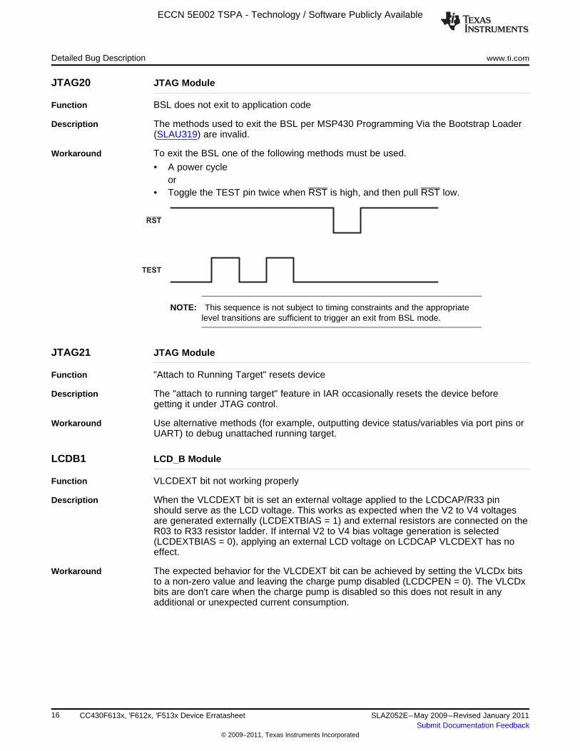
JTAG20 JTAG Module
Function BSL does not exit to application code
Description The methods used to exit the BSL per MSP430 Programming Via the Bootstrap Loader(SLAU319) are invalid.
Workaround To exit the BSL one of the following methods must be used.
• A power cycleor
• Toggle the TEST pin twice when RST is high, and then pull RST low.
NOTE: This sequence is not subject to timing constraints and the appropriatelevel transitions are sufficient to trigger an exit from BSL mode.
JTAG21 JTAG Module
Function "Attach to Running Target" resets device
Description The "attach to running target" feature in IAR occasionally resets the device beforegetting it under JTAG control.
Workaround Use alternative methods (for example, outputting device status/variables via port pins orUART) to debug unattached running target.
LCDB1 LCD_B Module
Function VLCDEXT bit not working properly
Description When the VLCDEXT bit is set an external voltage applied to the LCDCAP/R33 pinshould serve as the LCD voltage. This works as expected when the V2 to V4 voltagesare generated externally (LCDEXTBIAS = 1) and external resistors are connected on theR03 to R33 resistor ladder. If internal V2 to V4 bias voltage generation is selected(LCDEXTBIAS = 0), applying an external LCD voltage on LCDCAP VLCDEXT has noeffect.
Workaround The expected behavior for the VLCDEXT bit can be achieved by setting the VLCDx bitsto a non-zero value and leaving the charge pump disabled (LCDCPEN = 0). The VLCDxbits are don't care when the charge pump is disabled so this does not result in anyadditional or unexpected current consumption.
16 CC430F613x, 'F612x, 'F513x Device Erratasheet SLAZ052E–May 2009–Revised January 2011Submit Documentation Feedback
© 2009–2011, Texas Instruments Incorporated
ECCN 5E002 TSPA - Technology / Software Publicly Available
www.ti.com Detailed Bug Description
LCDB3 LCD_B Module
Function LCDFRMIFG set erroneously when LCDON changed from 1 to 0
Description The LCD_B frame interrupt flag (LCDFRMIFG) can be set erroneously when theinterrupt is enabled ((LCDFRMIE = 1) and the LCD_B module is switched off (LCDONchanged from 1 to 0).
Workaround Disable the frame interrupt before switching off the LCD_B module.
LCDB4 LCD_B Module
Function Write access to LCDBIV does not reset LCD IFGs
Description A write access to the LCDBIV register does not automatically reset all pending interruptflags.
Workaround Clear all interrupt flags in software by writing 0 to the lowest nibble of LCDBCTL1, wherethe flags are stored.
MPY1 Hardware Multiplier (MPY) Module
Function Save and Restore feature on MPY32 not functional
Description The MPY32 module uses the Save and Restore method which involves saving themultiplier state by pushing the MPY configuration/operand values to the stack beforeusing the multiplier inside an Interrupt Service Routine (ISR) and then restoring the stateby popping the configuration/operand values back to the MPY registers at the end of theISR. However due to the erratum the Save and Restore operation fails causing the writeoperation to the OP2H register right after the restore operation to be ignored as it is notpreceded by a write to OP2L register resulting in an invalid multiply operation.
Workaround None. Disable interrupts when writing to OP2L and OP2H registers.
NOTE: When using the C-compiler, the interrupts are automatically disabledwhile using the MPY32.
PMAP1 Port Mapping Controller
Function Port Mapping Controller does not clear unselected inputs to mapped module
Description The Port Mapping Controller provides the logical OR of all port mapped inputs to amodule (Timer, USCI, etc). If the PSEL bit (PxSEL.y) of a port mapped input is cleared,then the logic level of that port mapped input is latched to the current logic level of theinput. If the input is in a logical high state, then this high state is latched into the input ofthe logical OR. In this case, the input to the module is always a logical 1 regardless ofthe state of the selected input.
Workaround
• Drive input to the low state before clearing the PSEL bit of that input and switching toanother input source.or
• Use the Port Mapping Controller reconfiguration feature, PMAPRECFG, to selectinputs to a module and map only one input at a time.
17SLAZ052E–May 2009–Revised January 2011 CC430F613x, 'F612x, 'F513x Device ErratasheetSubmit Documentation Feedback
© 2009–2011, Texas Instruments Incorporated
ECCN 5E002 TSPA - Technology / Software Publicly Available
Detailed Bug Description www.ti.com
PMM8 Power Management Module
Function Supply current in LPM4.5 is unpredictable
Description Due to an unpredictable value of the supply current in LPM4.5, the mode should not beused.
Workaround None
PMM9 Power Management Module
Function False SVSxIFG events
Description The comparators of the SVS require a certain amount of time to stabilize and output acorrect result once re-enabled; this time is different for the Full Performance versus theNormal mode. The time to stabilize the SVS comparators is intended to be accounted forby a built-in event-masking delay of 2 µs when Full Performance mode is enabled.
However, the comparators of the SVS in Full Performance mode take longer than 2 µs tostabilize, so the possibility exists that a false positive will be triggered on the SVSH orSVSL. This results in the SVSxIFG flags being set and, depending on the configurationof SVSxPE bit, a POR can also be triggered .
Additionally, when the SVSxIFGs are set, all GPIOs are three-state; that is, floating untilthe SVSx comparators are settled.
The SVS IFGs are falsely set under the following conditions:
1. Wakeup from LPM2/3/4 when SVSxMD = 0 (default setting) and SVSxFP = 1. TheSVSx comparators are disabled automatically in LPM2/3/4 and are then re-enabledon return to active mode.
2. SVSx is turned on in full performance mode (SVSxFP = 1).3. A PUC/POR occurs after SVSx is disabled. After a PUC or POR, the SVSx are
enabled automatically, but the settling delay is not triggered. Based on the SVSxPEbit, this may lead to POR events until the SVS comparator is fully settled.
Workaround For each of the above listed conditions the following workarounds apply:
1. If the Full Performance mode is to be enabled for either the high-side or low-sideSVS comparators, the respective SVSxMD bits must be set (SVSxMD = 1) such thatthe SVS comparators are not temporarily shut off in LPM2/3/4. Note that this isequivalent to a 2 µA (typical) adder to the low-power mode current, per thedevice-specific data sheet, for each SVSx that remains enabled.
2. The SVSx must be turned on in normal mode (SVSxFP = 0). It can be reconfiguredto use full performance mode once the SVSx/SVMx delay has expired.
3. Ensure that SVSH and SVSL are always enabled.
PMM10 Power Management Module
Function SVS/SVM flags disabled after Power Up Clear reset
Description SVS/SVM interrupt flags are not set after a Power Up Clear (PUC) Reset if the SVS wasdisabled before the PUC reset was applied.
Workaround A write access to the intended SVSx register after PUC re-enables the SVS and SVMinterrupt flags.
18 CC430F613x, 'F612x, 'F513x Device Erratasheet SLAZ052E–May 2009–Revised January 2011Submit Documentation Feedback
© 2009–2011, Texas Instruments Incorporated
ECCN 5E002 TSPA - Technology / Software Publicly Available
www.ti.com Detailed Bug Description
PMM11 Power Management Module
Function DCO comes up fast on exit from LPM3 and LPM4
Description The DCO exceeds the programmed frequency of operation on exit from LPM3 and LPM4for a period of time up to 6 µs. This behavior is masked from affecting code execution bydefault: SVSL and SVML run in normal-performance mode and mask CPU execution for150 µs on wakeup from LPM3 and LPM4.
However, when the low-side SVS and the SVM are disabled or operating infull-performance mode (that is, SVMLE = 0, SVSLE = 0, or SVMLFP = 1, SVSLFP = 1)and MCLK is sourced from the internal DCO running over 5.5 MHz, 8 MHz, 13 MHz, or16.5 MHz at core voltage levels 0, 1, 2, or 3, respectively, the mask lasts only 2 µs.MCLK is therefore susceptible to run out of spec for 4 µs.
Workaround Set the MCLK divide bits in the Unified Clock System Control 5 Register (UCSCTL5) todivide MCLK by two prior to entering LPM3 or LPM4 (set DIVMx = 001). This preventsMCLK from running out of spec when the CPU wakes from the low-power mode.Following the wakeup from the low-power mode, wait 32, 48, 80, or 100 cycles for corevoltage levels 0, 1, 2, or 3, respectively, before resetting DIVMx to zero and runningMCLK at full speed [for example, __delay_cycles(100)].
PMM12 Power Management Module
Function SMCLK comes up fast on exit from LPM3 and LPM4
Description The DCO exceeds the programmed frequency of operation on exit from LPM3 and LPM4for a period of time up to 6 µs. When SMCLK is sourced by the DCO, it is not masked onexit from LPM3 or LPM4. Therefore, SMCLK exceeds the programmed frequency ofoperation on exit from LPM3 and LPM4 for up to 6 µs. The increased frequency has thepotential to change the expected timing behavior of peripherals that select SMCLK asthe clock source.
Workaround
• Use XT2 as the SMCLK oscillator source instead of the DCO.or
• Do not disable the clock request bit for SMCLKREQEN in the Unified Clock SystemControl 8 Register (UCSCTL8). This means that all modules that depend on SMCLKto operate successfully should be halted or disabled before entering LPM3 or LPM4.If the increased frequency prevents the proper function of an affected module, wait32, 48, 80, or 100 cycles for core voltage levels 0, 1, 2, or 3, respectively, beforere-enabling the module [for example, __delay_cycles(100)].
PMM14 Power Management Module
Function Increasing the core level when SVS/SVM low side is configured in full-performancemode causes device reset
Description When the SVS/SVM low side is configured in full performance mode(SVSMLCTL.SVSLFP = 1), the settling time delay for the SVS comparators isapproximately 2 µs. When increasing the core level in full-performance mode; the corevoltage does not settle to the new level before the settling time delay of the SVS/SVMcomparator expires. This results in a device reset.
Workaround When increasing the core level, enable the SVSSV/M low side in normal mode(SVSMLCTL.SVSLFP = 0). This provides a settling time delay of approximately 150 µs,allowing the core sufficient time to increase to the expected voltage before the delayexpires.
19SLAZ052E–May 2009–Revised January 2011 CC430F613x, 'F612x, 'F513x Device ErratasheetSubmit Documentation Feedback
© 2009–2011, Texas Instruments Incorporated
ECCN 5E002 TSPA - Technology / Software Publicly Available
Detailed Bug Description www.ti.com
PORT15 Digital I/O Module, Port 1 and 2
Function In-system debugging causes the PMALOCKED bit to be always set
Description The port mapping controller registers cannot be modified when single-stepping or haltingat break points between a valid password write to the PMAPWD register and theexpected lock of the port mapping (PMAP) registers. This causes the PMAPLOCKED bitto remain set and not clear as expected.
NOTE: This erratum only applies to in-system debugging and is not applicablewhen operating in free-running mode.
Workaround Do not single step through or place break points in the port mapping configurationsection of code.
RF1A1 RF1A Module
Function The PLL lock detector output is not 100% reliable
Description The PLL lock detector output is not 100% reliable and might toggle even if the PLL is inlock. The PLL is in lock if the lock detector output has a positive transition or isconstantly logic high. The PLL is not in lock if the lock detector output is constantly logiclow. It is not recommended to check for PLL lock by reading PKTSTATUS[0] withGDOx_CFG = 0x0A or PKTSTATUS[2] register with GDOx_CFG = 0x0A (x = 0 or 2).
Workaround PLL lock can be checked reliably by these methods:
• Program register IOCFGx.GDOx_CFG = 0x0A and use the lock detector outputavailable on the GDOx pin as an interrupt for the MCU. A positive transition on theGDOx pin means that the PLL is in lock. It is important to disable for interrupt whenwaking the chip from SLEEP state as the wake-up might cause the GDOx pin totoggle when it is programmed to output the lock detector.or
• Read register FSCAL1. The PLL is in lock if the register content is different from0x3F.
With both of the above workarounds the CC1101 PLL calibration should be carried outwith the correct settings for TEST0. VCO_SEL_CAL_EN andFSCAL2.VCO_CORE_H_EN. These settings are depending on the operating frequencyand are calculated automatically by SmartRF® Studio.
Note that the TEST0 register content is not retained in SLEEP state, and thus it isnecessary to write to this register as described here when returning from the SLEEPstate.
20 CC430F613x, 'F612x, 'F513x Device Erratasheet SLAZ052E–May 2009–Revised January 2011Submit Documentation Feedback
© 2009–2011, Texas Instruments Incorporated
ECCN 5E002 TSPA - Technology / Software Publicly Available
www.ti.com Detailed Bug Description
RF1A2 RF1A Module
Function RXFIFO overflow flag does not work as intended
Description In addition to having a 64-byte long RX FIFO, the CC430 has a one byte long pre-fetchbuffer between the FIFO and the RF1A module. It also has buffers for status registersand CRC bytes. If more than 65 bytes have been received (the FIFO and the pre-fetchbuffer are full) without reading the RX FIFO, the radio will enter RXFIFO_OVERFLOWstate. There are, however, some cases where the radio will be stuck in RX state insteadof entering RXFIFO_OVERFLOW state. Below is a table showing the register settingsthat will cause this problem. APPEND_STATUS is found in the PKTCTRL1 register, andCRC_EN is found in the PKTCTRL0 register.
Setting IOCFGx=0x06 should mean that the GDO signal is deasserted when theRXFIFO overflows. In the cases where the radio is stuck in RX state, the GDOx pin willnot be deasserted.
When the radio is stuck in this RX state it draws current as if it was in the RX state, but itwill not be able to receive any more data. The only way to get out of this state is to issuean SIDLE strobe and then flush the FIFO (SFRX).
Workaround In applications where the packets are short enough to fit in the RX FIFO and one wantsto wait for the whole packet to be received before starting to read the RX FIFO, forvariable packet length mode (PKTCTRL0.LENGTH_CONFIG=1) the PKTLEN registershould be set to 61 to make sure the whole packet including status bytes are 64 bytes orless (length byte (61) + 61 payload bytes + 2 status bytes = 64 bytes) or PKTLEN = 62 iffixed packet length mode is used (PKTCTRL0.LENGTH_CONFIG=0). In applicationwhere the packets do not fit in the RX FIFO, one must start reading the RX FIFO beforeit reaches its limit (64 bytes).
RF1A3 RF1A Module
Function Extra Byte Transmitted in TX
Description If transmission is aborted (exits TX mode) during the transmission of the first half of anybyte, there is a repetition of the first byte in the next transmission. This issue is causedby a state machine controlling the mod_rd_data signal in the modulator. This signalasserts at the start of transmission of each full byte, then deasserts after half the bytehas been transmitted. If the transmission is aborted after a byte has started but beforehalf the byte is transmitted, this signal remains asserted and the first byte in the nexttransmission is repeated.
Workaround As long as the packet handling features of the CC430 are used, this is not a problembecause the chip always exits TX mode after the transmission of the last bit in the lastbyte of the packet. If, however, the packet handling features are disabled(MDMCFG2.SYNC_MODE=0) and TX mode is manually exited by strobing IDLE, ensurethat the IDLE strobe is being issued after clocking out 12 dummy bits (8 dummy bits arenecessary due to the TX latency, but because this would mean that transmission isaborted within the first half of a byte, 4 extra bits are added).
21SLAZ052E–May 2009–Revised January 2011 CC430F613x, 'F612x, 'F513x Device ErratasheetSubmit Documentation Feedback
© 2009–2011, Texas Instruments Incorporated
ECCN 5E002 TSPA - Technology / Software Publicly Available
Detailed Bug Description www.ti.com
RF1A5 RF1A Module
Function FIFO Radio Core Interrupt may be triggered independent of the RFINx condition beingmet
Description The radio core interrupt flags (RFIFGx) may be set and could generate a radio coreinterrupt although the corresponding radio input (RFINx) signal condition has not beenmet.
This is true for the FIFO Mapped Control Signals RFIFG3, RFIFG4, RFIFG5, RFIFG6,RFIFG7, RFIFG8, RFIFG9 (negative edge), and RFIFG10 (negative edge).
Workaround When handling the radio core interrupts RFIFG3 to RFIFG10, proceed with the ISR onlyafter verifying that the RFINx signal respective to the RFIFGx flag is active.
RF1A6 RF1A Module
Function LVERR flag set when radio in SLEEP or IDLE and VCORE = 0 or 1
Description The low-voltage error flag (LVERR) is set when the radio is in the SLEEP or IDLE stateand VCORE = 0 or 1, which is contrary to the behavior specified in the CC430 User'sGuide.
Workaround None
RTC4 RTC Module
Function RTC clock calibration maybe offset by +2 ppm
Description When using the RTC clock calibration feature, the RTCCLK frequency maybe offset by+2 ppm after the calibration procedure is completed. This affects both up and downcalibration.
Workaround None
SYS16 System Module
Function Fast VCC ramp after device power up may cause a reset
Description At initial power-up, after VCC crosses the bownout threshold and reaches a constantlevel, an abrupt ramp of VCC at a rate dV/dT > 1V/100µs can cause a brownout conditionto be incorrectly detected even though VCC does not fall below the brownout threshold.This causes the device to undergo a reset.
Workaround Use a controlled VCC ramp to power the device.
22 CC430F613x, 'F612x, 'F513x Device Erratasheet SLAZ052E–May 2009–Revised January 2011Submit Documentation Feedback
© 2009–2011, Texas Instruments Incorporated
ECCN 5E002 TSPA - Technology / Software Publicly Available
www.ti.com Detailed Bug Description
TAB23 Timer_A/Timer_B Module
Function TAxR read can be corrupted when TAxR = TAxCCR0
Description When a timer in Up mode is stopped and the counter register (TAxR) is equal to theTAxCCR0 value, a read of the TAR register may return an unexpected result.
Workaround
• Use Up/Down mode instead of Up mode.or
• In Up mode, use the timer interrupt instead of halting the counter and reading out thevalue in TAxR.or
• When halting the timer counter in 'Up' mode, reinitialize the timer before starting torun again.
UCS6 Universal Clock System Module
Function USCI source clock does not turn off in LPM3/4 when UART is idle
Description The USCI clock source (ACLK/SMCLK) remains enabled in LPM3 and LPM4 when theUSCI is configured in UART mode and the communication is idle (UCSWRST = 0 but noTX or RX currently executing). This is contrary to the expected automatic clock activationdescribed in the user's guide and can lead to higher current consumption in low-powermodes, depending on the oscillator that feeds ACLK/SMCLK.
Workaround Use the oscillator that is already active in LPM3 (ACLK) to source the USCI and use thelow-power baud rate generator (UCOS16 = 0). For UART baud rates where a fastSMCLK sourced by the internal DCO is required, use LPM0 instead of LPM3.
UCS7 Universal Clock System Module
Function DCO drifts when servicing short ISRs when in LPM0 or exiting active from ISRs for shortperiods of time
Description The FLL uses two rising edges of the reference clock to compare against the DCOfrequency and decide on the required modifications to the DCOx and MODx bits. If thedevice is in a low-power mode with FLL disabled (LPM0 with DCO not sourcingACLK/SMCLK or LPM2, LPM3, LPM4 where SCG1 bit is set) and enters a state thatenables FLL (enter ISR from LPM0/LPM2 or exit active from ISRs) for a period less thanthree reference clock cycles, then the FLL will cause the DCO to drift.
This occurs because the FLL immediately begins comparing an active DCO with itsreference clock and making the respective modifications to the DCOx and MODx bits. Ifthe FLL is not given sufficient time to capture a full reference clock cycle (two referenceclock periods) and adjust accordingly (one reference clock period), then the DCO keepsdrifting each time the FLL is enabled.
Workaround
• If DCO is not sourcing ACLK or SMCLK in the application, use LPM1 instead ofLPM0 to make sure FLL is disabled when interrupt service routine is serviced.or
• When exiting active from ISRs, insert a delay of at least three reference clockperiods. To save on power budget, the three reference clock periods could also bespent in LPM0 with TimerA or TimerB using ACLK/SMCLK sourced from DCO. Thisway, the FLL and DCO are still active in LPM0.
23SLAZ052E–May 2009–Revised January 2011 CC430F613x, 'F612x, 'F513x Device ErratasheetSubmit Documentation Feedback
© 2009–2011, Texas Instruments Incorporated
ECCN 5E002 TSPA - Technology / Software Publicly Available
Detailed Bug Description www.ti.com
UCS9 Universal Clock System Module
Function Digital Bypass mode prevents entry into LPM4
Description When entering LPM4, if an external digital input applied to XT1 in HF mode or XT2 is notturned off, the PMM does not switch to low-current mode causing higher than expectedpower consumption.
Workaround Before entering LPM4:
• Switch to a clock source other than external bypass digital inputor
• Turn off external bypass mode (UCSCTL6.XT1BYPASS = 0)
UCS10 Universal Clock System Module
Function Modulation causes shift in DCO frequency
Description When the FLL is enabled, the DCO frequency can be tracked automatically by modifyingthe DCOx and MODx bits. The MODx bits switch between the frequency selected by theDCO bits and the next higher frequency set by (DCO + 1). The erroneous behavior isseen when the FLL is tracking close to a DCO step boundary and the MOD counter isexpected to rollover but, instead, the DCO bits increment and the MOD bits decrement.This causes the DCO to shift by up to 12% and remain at an increased frequency untilapproximately 15 REFCLK cycles have elapsed. The frequency reverts to the expectedvalue immediately afterward.
For example, the modulator moves from DCOx = n and MODx = 31 to DCOx = n + 1and MODx = 30, causing a large increase in the DCO frequency.
Applications could be impacted as follows:
• When using the DCO frequency for asynchronous serial communication and timeroperation, the effect can be seen as corrupted data or incorrect timing events.
Workaround
• Change the clock source from the DCO to an external crystal oscillator (for example,XT1 or XT2, if available on the device) during the critical timing phase.or
• Implement a software FLL, comparing the DCO frequency to a known reference suchas REFO or LFXT1 using a timer capture and tuning the value of the DCO and MODbits periodically.or
• Execute the following sequence in periodic intervals.
1. Disable peripherals sourced by the DCO such as UART and timer.2. Turn on the FLL.3. Wait the worst case settling time of 32 × 32 × fFLLREFCLK to allow the FLL to lock to
the target frequency.4. Turn off the FLL.5. Compare the DCO frequency to a known reference such as REFO or LFXT1
using a timer capture.
• If the DCO frequency is higher than expected, repeat from step (2) until thefrequency reaches the expected range.
• Else proceed with code execution.
See the application report UCS10 Guidance (SLAA489) for information regardingworking with this erratum. This erratum does not affect proper operation of the CPUwhen MCLK = DCO/FLL and is set to the maximum clock frequency specified in thedevice-specific data sheet.
24 CC430F613x, 'F612x, 'F513x Device Erratasheet SLAZ052E–May 2009–Revised January 2011Submit Documentation Feedback
© 2009–2011, Texas Instruments Incorporated
ECCN 5E002 TSPA - Technology / Software Publicly Available
www.ti.com Detailed Bug Description
USCI26 USCI Module
Function tbuf parameter violation in I2C multi-master mode
Description In multi-master I2C systems, the timing parameter tbuf (bus free time between a stopcondition and the following start) is not ensured to match the I2C specification of 4.7 µsin standard mode and 1.3 µs in fast mode. If the UCTXSTT bit is set during a running I2Ctransaction, the USCI module waits and issues the start condition on bus release,causing the violation to occur.
NOTE: It is recommended to check if UCBBUSY bit is cleared before settingUCTXSTT = 1.
Workaround None
WDG4 Watchdog Module
Function The WDT failsafe can be disabled
Description The UCS is capable of masking clock requests (ACLK, SMCLK, MCLK) from peripheralmodules; see request enable (REQEN) bits in the UCS control register, UCSCTL8.
The clock request logic of the UCS is used by the WDT module to ensure a fail-safeclock source in all low-power modes. Therefore, de-asserting the request enable bit ofthe watchdog clock source (xCLKREQEN = 0) allows the respective clock to be disabledupon entry into a low-power mode. Without an active clock source, the WDT timer stopsincrementing and a watchdog event does not occur.
Workaround None
25SLAZ052E–May 2009–Revised January 2011 CC430F613x, 'F612x, 'F513x Device ErratasheetSubmit Documentation Feedback
© 2009–2011, Texas Instruments Incorporated
ECCN 5E002 TSPA - Technology / Software Publicly Available
www.ti.com
Appendix A Prior Revisions
None
26 Prior Revisions SLAZ052E–May 2009–Revised January 2011Submit Documentation Feedback
© 2009–2011, Texas Instruments Incorporated
ECCN 5E002 TSPA - Technology / Software Publicly Available
www.ti.com Revision History
Revision History
Changes from D Revision (September 2010) to E Revision .......................................................................................... Page
• Updated ADC27 .......................................................................................................................... 4• Added ADC29 ............................................................................................................................. 4• Added FLASH37 ........................................................................................................................ 15• Added PMM14 ........................................................................................................................... 19• Added SYS16 ........................................................................................................................... 22• Added UCS10 ........................................................................................................................... 24
NOTE: Page numbers for previous revisions may differ from page numbers in the current version.
27SLAZ052E–May 2009–Revised January 2011 Revision HistorySubmit Documentation Feedback
© 2009–2011, Texas Instruments Incorporated

IMPORTANT NOTICE
Texas Instruments Incorporated and its subsidiaries (TI) reserve the right to make corrections, modifications, enhancements, improvements,and other changes to its products and services at any time and to discontinue any product or service without notice. Customers shouldobtain the latest relevant information before placing orders and should verify that such information is current and complete. All products aresold subject to TI’s terms and conditions of sale supplied at the time of order acknowledgment.
TI warrants performance of its hardware products to the specifications applicable at the time of sale in accordance with TI’s standardwarranty. Testing and other quality control techniques are used to the extent TI deems necessary to support this warranty. Except wheremandated by government requirements, testing of all parameters of each product is not necessarily performed.
TI assumes no liability for applications assistance or customer product design. Customers are responsible for their products andapplications using TI components. To minimize the risks associated with customer products and applications, customers should provideadequate design and operating safeguards.
TI does not warrant or represent that any license, either express or implied, is granted under any TI patent right, copyright, mask work right,or other TI intellectual property right relating to any combination, machine, or process in which TI products or services are used. Informationpublished by TI regarding third-party products or services does not constitute a license from TI to use such products or services or awarranty or endorsement thereof. Use of such information may require a license from a third party under the patents or other intellectualproperty of the third party, or a license from TI under the patents or other intellectual property of TI.
Reproduction of TI information in TI data books or data sheets is permissible only if reproduction is without alteration and is accompaniedby all associated warranties, conditions, limitations, and notices. Reproduction of this information with alteration is an unfair and deceptivebusiness practice. TI is not responsible or liable for such altered documentation. Information of third parties may be subject to additionalrestrictions.
Resale of TI products or services with statements different from or beyond the parameters stated by TI for that product or service voids allexpress and any implied warranties for the associated TI product or service and is an unfair and deceptive business practice. TI is notresponsible or liable for any such statements.
TI products are not authorized for use in safety-critical applications (such as life support) where a failure of the TI product would reasonablybe expected to cause severe personal injury or death, unless officers of the parties have executed an agreement specifically governingsuch use. Buyers represent that they have all necessary expertise in the safety and regulatory ramifications of their applications, andacknowledge and agree that they are solely responsible for all legal, regulatory and safety-related requirements concerning their productsand any use of TI products in such safety-critical applications, notwithstanding any applications-related information or support that may beprovided by TI. Further, Buyers must fully indemnify TI and its representatives against any damages arising out of the use of TI products insuch safety-critical applications.
TI products are neither designed nor intended for use in military/aerospace applications or environments unless the TI products arespecifically designated by TI as military-grade or "enhanced plastic." Only products designated by TI as military-grade meet militaryspecifications. Buyers acknowledge and agree that any such use of TI products which TI has not designated as military-grade is solely atthe Buyer's risk, and that they are solely responsible for compliance with all legal and regulatory requirements in connection with such use.
TI products are neither designed nor intended for use in automotive applications or environments unless the specific TI products aredesignated by TI as compliant with ISO/TS 16949 requirements. Buyers acknowledge and agree that, if they use any non-designatedproducts in automotive applications, TI will not be responsible for any failure to meet such requirements.
Following are URLs where you can obtain information on other Texas Instruments products and application solutions:
Products Applications
Audio www.ti.com/audio Communications and Telecom www.ti.com/communications
Amplifiers amplifier.ti.com Computers and Peripherals www.ti.com/computers
Data Converters dataconverter.ti.com Consumer Electronics www.ti.com/consumer-apps
DLP® Products www.dlp.com Energy and Lighting www.ti.com/energy
DSP dsp.ti.com Industrial www.ti.com/industrial
Clocks and Timers www.ti.com/clocks Medical www.ti.com/medical
Interface interface.ti.com Security www.ti.com/security
Logic logic.ti.com Space, Avionics and Defense www.ti.com/space-avionics-defense
Power Mgmt power.ti.com Transportation and www.ti.com/automotiveAutomotive
Microcontrollers microcontroller.ti.com Video and Imaging www.ti.com/video
RFID www.ti-rfid.com Wireless www.ti.com/wireless-apps
RF/IF and ZigBee® Solutions www.ti.com/lprf
TI E2E Community Home Page e2e.ti.com
Mailing Address: Texas Instruments, Post Office Box 655303, Dallas, Texas 75265Copyright © 2011, Texas Instruments Incorporated