Embed Size (px)
Citation preview
Noise XT datasheet v3 SLC ultra low jitter clock synthesizer 1 / 8
SLC ultra low jitter Clock Synthesizer 2 MHz to 7 GHz
Datasheet
The SLC is a very affordable single or dual clock 7 GHz synthesizer that exhibits outstanding phase noise and jitter performance in a very small package. With -170 dBc/Hz phase noise floor at 10 MHz, the SLC is the lowest phase noise compact clock synthesizer of the industry that can help you challenge tomorrow’s requirements for high speed, high bandwidth Software Defined Radio applications (SDR) and low phase noise PLL and DDS synthesis. Its high power output is ideal to drive mixers’ LO inputs or high-speed digital clocks. Its very low jitter profile makes ADC and DAC testing more accurate. This source is often cleaner than a crystal oscillator and can offer a high SNR, up to 135 dB. USB control helps you seamlessly integrate this tool in your test project or clock distribution architecture. Both synthesizers can be controlled completely independently and do not share any common reference frequencies. However, when coherent signals are required, they can be locked to each other with the help of their 10 MHz reference signals. Optional ultra low phase noise OCVCXO allows the synthesizers to reach their best specification and if this is not enough, the external 10 MHz reference input will extends its long term frequency stability (Allan variance) to the one of atomic clocks.
Noise XT datasheet v3 SLC ultra low jitter clock synthesizer 2 / 8
Specifications below describe the RF inputs and Outputs for each synthesizer. When 2 synthesizers are present, there are two sets of inputs and outputs.
RF Output Specifications Description Specification Output Frequency 2 MHz to 7 GHz Frequency Resolution 0.001 Hz Frequency Switching time (list mode) < 1 ms or < 150 us (option) Frequency Dwell time 2 ms to 20,000 ms Output Level -30 dBm to +13 dBm (to +17 dBm in 4 MHz-4
GHz) Level Resolution 0.5 dB Non-Harmonic spurious -70 dBc above 1 kHz offset (-76dBc typ) Modulation DC coupled FM (8ppm/V VCXO, 0.6ppm/V
OCVCXO option, 1kHz BW max) Output connector SMA female, 50 Ohms
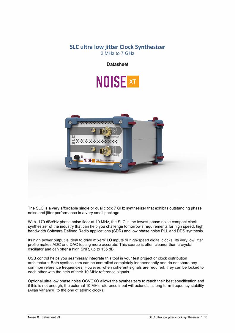
Typical Output Power Level Below is the maximum RF output power level for the whole band. The SLC is capable of +18 dBm in most of its band and drive power demanding applications.
Phase Noise performance Typical Phase Noise with standard phase noise installed (VCXO). dBc/Hz vs offset (Hz) 100 1k 10k 100k 1M Floor
10 MHz -130 -160 -168 -170 -170 -170
100 MHz -110 -141 -154 -156 -158 -164
1 GHz -94 -123 -134 -137 -142 -164
2 GHz -88 -117 -128 -126 -129 -160
4 GHz -82 -111 -123 -125 -130 -160
7 GHz -76 -105 -117 -119 -121 -155 please add +5dB for guaranteed performance
10
12
14
16
18
20
22
2 4 8 16 31 63 125 250 500 1,000 2,000 3,000 3,500 4,000 4,820 5,809 7,000
Typical Max RF power (dBm)
Noise XT datasheet v3 SLC ultra low jitter clock synthesizer 3 / 8
Typical Phase Noise with ultra low phase noise option installed (OCVCXO). dBc/Hz vs offset (Hz) 100 1k 10k 100k 1M Floor
10 MHz -150 -160 -168 -171 -175 -175
100 MHz -133 -147 -155 -157 -158 -169
1 GHz -113 -127 -136 -137 -142 -164
2 GHz -108 -121 -130 -131 -134 -160
4 GHz -102 -115 -124 -125 -129 -164
7 GHz -97 -110 -119 -121 -122 -157 please add +5dB for guaranteed performance
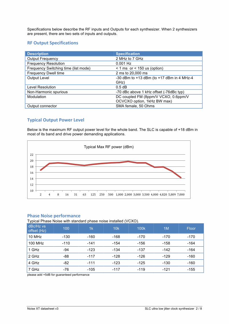
Typical Phase Noise plots at various frequencies with ultra low phase noise OCVCXO option
Noise XT datasheet v3 SLC ultra low jitter clock synthesizer 4 / 8
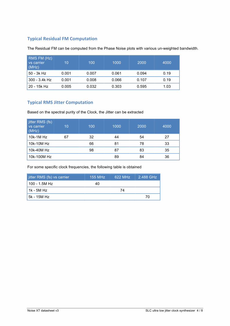
Typical Residual FM Computation The Residual FM can be computed from the Phase Noise plots with various un-weighted bandwidth. RMS FM (Hz) vs carrier (MHz)
10 100 1000 2000 4000
50 - 3k Hz 0.001 0.007 0.061 0.094 0.19
300 - 3.4k Hz 0.001 0.008 0.066 0.107 0.19
20 - 15k Hz 0.005 0.032 0.303 0.595 1.03
Typical RMS Jitter Computation Based on the spectral purity of the Clock, the Jitter can be extracted jitter RMS (fs) vs carrier (MHz)
10 100 1000 2000 4000
10k-1M Hz 67 32 44 54 27
10k-10M Hz 66 81 78 33
10k-40M Hz 98 87 83 35
10k-100M Hz 89 84 36 For some specific clock frequencies, the following table is obtained jitter RMS (fs) vs carrier 155 MHz 622 MHz 2.488 GHz
100 - 1.5M Hz 40
1k - 5M Hz 74
5k - 15M Hz 70
Noise XT datasheet v3 SLC ultra low jitter clock synthesizer 5 / 8
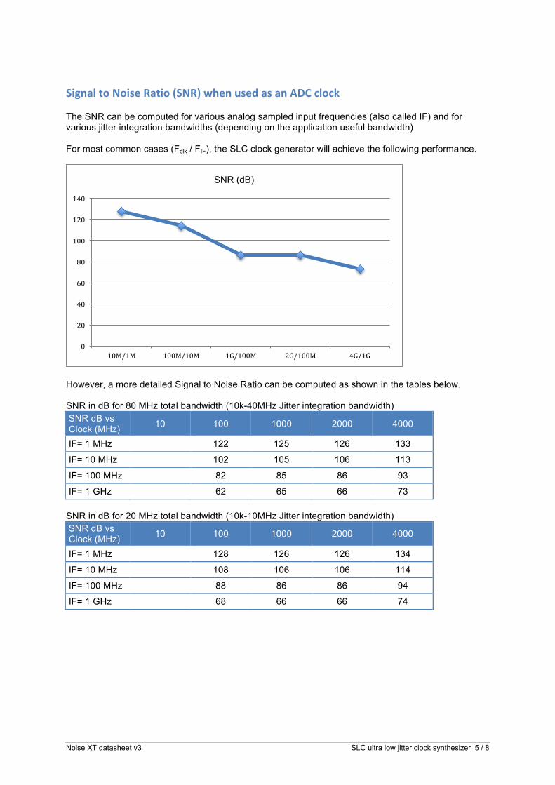
Signal to Noise Ratio (SNR) when used as an ADC clock The SNR can be computed for various analog sampled input frequencies (also called IF) and for various jitter integration bandwidths (depending on the application useful bandwidth) For most common cases (Fclk / FIF), the SLC clock generator will achieve the following performance.
However, a more detailed Signal to Noise Ratio can be computed as shown in the tables below. SNR in dB for 80 MHz total bandwidth (10k-40MHz Jitter integration bandwidth) SNR dB vs Clock (MHz) 10 100 1000 2000 4000
IF= 1 MHz 122 125 126 133
IF= 10 MHz 102 105 106 113
IF= 100 MHz 82 85 86 93
IF= 1 GHz 62 65 66 73 SNR in dB for 20 MHz total bandwidth (10k-10MHz Jitter integration bandwidth) SNR dB vs Clock (MHz) 10 100 1000 2000 4000
IF= 1 MHz 128 126 126 134
IF= 10 MHz 108 106 106 114
IF= 100 MHz 88 86 86 94
IF= 1 GHz 68 66 66 74
0
20
40
60
80
100
120
140
10M/1M 100M/10M 1G/100M 2G/100M 4G/1G
SNR (dB)
Noise XT datasheet v3 SLC ultra low jitter clock synthesizer 6 / 8
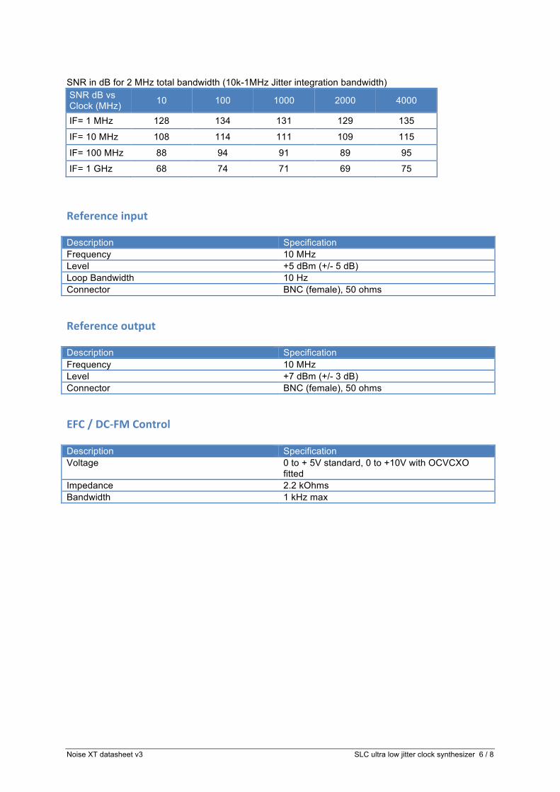
SNR in dB for 2 MHz total bandwidth (10k-1MHz Jitter integration bandwidth) SNR dB vs Clock (MHz) 10 100 1000 2000 4000
IF= 1 MHz 128 134 131 129 135
IF= 10 MHz 108 114 111 109 115
IF= 100 MHz 88 94 91 89 95
IF= 1 GHz 68 74 71 69 75
Reference input Description Specification Frequency 10 MHz Level +5 dBm (+/- 5 dB) Loop Bandwidth 10 Hz Connector BNC (female), 50 ohms
Reference output Description Specification Frequency 10 MHz Level +7 dBm (+/- 3 dB) Connector BNC (female), 50 ohms
EFC / DC-‐FM Control Description Specification Voltage 0 to + 5V standard, 0 to +10V with OCVCXO
fitted Impedance 2.2 kOhms Bandwidth 1 kHz max
Noise XT datasheet v3 SLC ultra low jitter clock synthesizer 7 / 8
Programming features Description Supplemental information Modes CW and Sweep, List through programming Interface National Instruments LabView® examples and
driver for USB Windows® OS compatible Graphical User Interface for Windows®
General Information The connections described below are shared between the synthesizers. Only one set is present, regardless of the number of synthesizers present in the SLC. Rear panel information Description Supplemental information USB 1 ports (USB 2.0) DC power +10 to +24 V input port Power 15W per synthesizer FAN Intake Synthesizer environment and dimensions Description Supplemental information Operating environment Temperature +10 degC to +40 degC Humidity RH 20% to 80% at wet bulb temp.<29 degC
(non-condensing) Altitude 0 to +2 000 m Non-operating storage environment Temperature -10 degC to +60 degC Humidity RH 20% to 90% at wet bulb temp.<40 degC
(non-condensing) Altitude -427 to +4 810 m Vibration 0.5 G maximum, 5 Hz to 500 Hz Instrument dimensions See figure below Weight (NET) < 1 kg for dual configuration
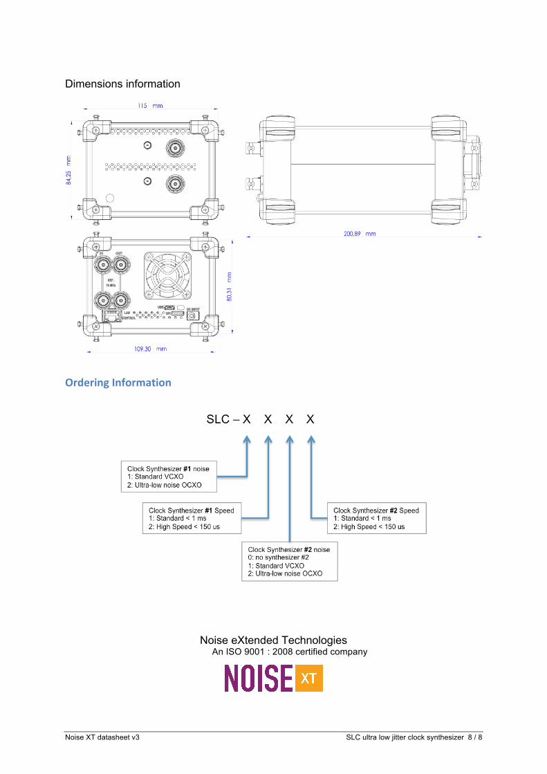
Noise XT datasheet v3 SLC ultra low jitter clock synthesizer 8 / 8
Dimensions information
Ordering Information
Noise eXtended Technologies An ISO 9001 : 2008 certified company