Embed Size (px)
Citation preview

SLIP-2008, Newcastle upon Tyne, UKApril 5, 2008
Parallel vs. SerialOn-Chip Communication
Rostislav (Reuven) Dobkin
Arkadiy Morgenshtein
Avinoam Kolodny
Ran Ginosar
Technion – Israel Institute of TechnologyElectrical Engineering Department
VLSI Systems Research Center

2/33
Presentation Outline
Motivation– Parallel links limitations– Novel high-speed serial links
Link Architectures– "Register-Pipelined" and "Wave-pipelined" parallel links– Single gate-delay serial link
Comparative study: parallel vs. serial– Analytical models – Scalability– 65nm case study
3/33
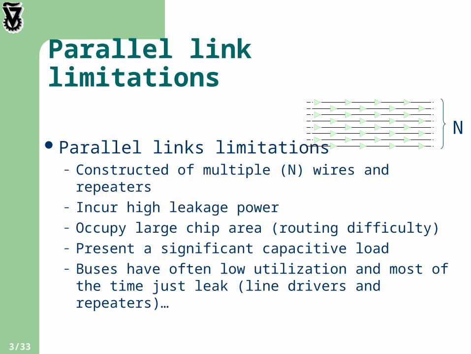
Parallel link limitations
Parallel links limitations– Constructed of multiple (N) wires and repeaters– Incur high leakage power– Occupy large chip area (routing difficulty)– Present a significant capacitive load– Buses have often low utilization and most of the
time just leak (line drivers and repeaters)…
N
4/33
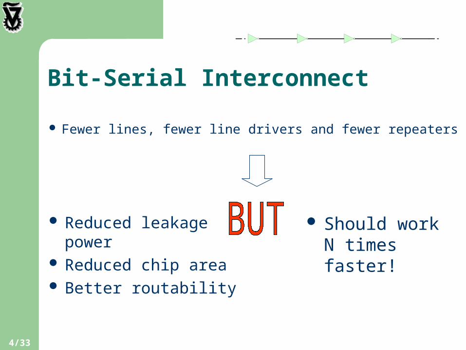
Bit-Serial Interconnect
Fewer lines, fewer line drivers and fewer repeaters
Reduced leakage power
Reduced chip area Better routability
Should work N times faster!

5/33
Serial Link
Standard serial links are very slow Hope lies in novel serial links
– Data cycle of a few gate-delays (inverter FO4 delay)
This work considers the fastest serial link– With single gate-delay data cycle (d4)
Our target: to show that novel serial link outperforms the parallel one for
– Long ranges– Advanced technology nodes

6/33
Method
Choose – Parallel link implementation representatives – Serial link implementation representatives
Compare the parallel and serial link approaches in terms of:– Area– Power– Latency– Technology scaling

7/33
"Register-Pipelined" Parallel Link
1
2
N
CLKT
1
2
N
CLKR
1
2
N
Fully synchronous Interconnect as combinational logic between registers Source synchronous or global clock
High cost for high bit rates!
8/33
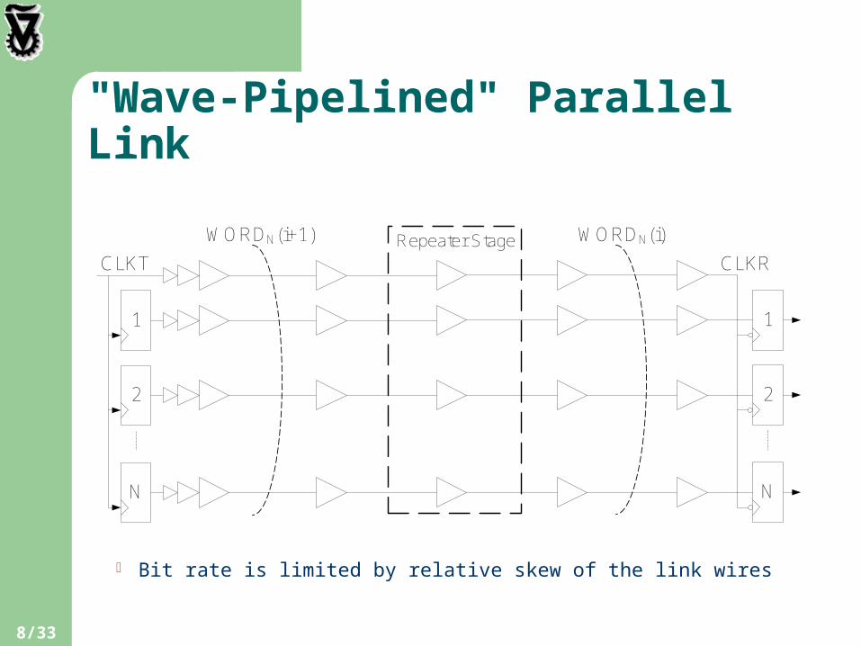
"Wave-Pipelined" Parallel Link
1
2
N
CLKRRepeater Stage
1
2
N
CLKT
WORDN(i+1) WORDN(i)
Bit rate is limited by relative skew of the link wires

9/33
Crosstalk Mitigation andPower Reduction
Shielding / Spacing Staggered repeaters Interleaved bi-directional lines Asynchronous signaling Data encoding Data pattern recognition with special worst-case handling
This work analyzes the two extremes of shielding:– Unshielded wires (a)– Fully-shielded wires (b)
(a) (b)

10/33
Single Gate-Delay Serial Link
Transition signaling instead of sampling– Two-phase NRZ Level Encoded Dual Rail (LEDR)
asynchronous protocol, a.k.a. data-strobe (DS)
Acknowledge per word instead of per bit Wave-pipelining over channel Differential encoding (DS-DE, IEEE1355-95) Low-latency synchronizers
Sender Receiver
Word Ack
Bit-Serial ChannelSynchr. Synchr.Serializer
& LEDREncoder
DeSerializer& LEDRDecoder
P
S
R. Dobkin, et al., High Rate Wave-Pipelined Asynchronous On-Chip Bit-Serial Data Link, ASYNC07

11/33
Analytical Models
Parallel and Serial Link Bit Rates
Please refer to the paper for details on the exact analytical models employed in the work

12/33
Parallel Link Bit Rate Limitations (1)
A. Fastest available clock– Ring oscillator limitation: 8d4
– Fast processors: 11d4 (e.g. CELL)– Standard SoC/ASIC: 100-400d4
B. Synchronization Latency– May take several clocks in case of asynchronous
clock relation
C. Clock uncertainty– Extended critical path
RESET
CLK
DOUT
SOURCE
LEAF
13/33
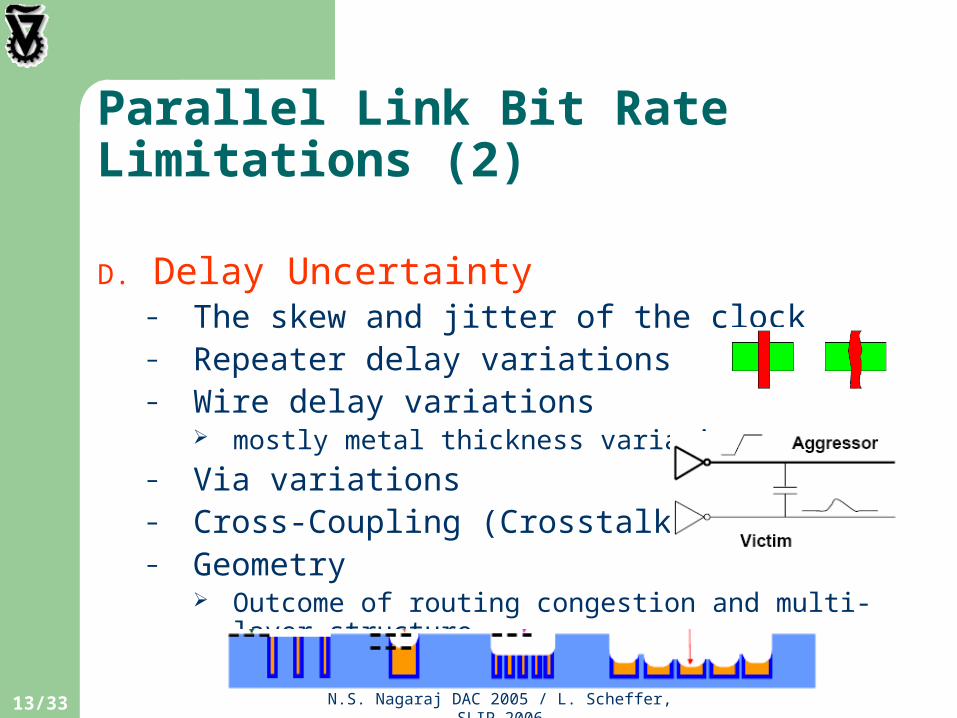
Parallel Link Bit Rate Limitations (2)
D. Delay Uncertainty– The skew and jitter of the clock– Repeater delay variations – Wire delay variations
mostly metal thickness variations
– Via variations– Cross-Coupling (Crosstalk)– Geometry
Outcome of routing congestion and multi-layer structure
N.S. Nagaraj DAC 2005 / L. Scheffer, SLIP 2006

14/33
Parallel Link Minimal Clock Cycle (1)
LinkLength
TSU+2DCLK TH+2DCLK
Maximal Data Delay, dMAX
Minimal Data Delay, dMIN
CLKT
DCLK
Notations from W.P. Burleson, et al., Wave-Pipelining: A Tutorial and Research Survey, TVLSI, 1998
2 ( ) 4CLK MAX MIN CLK SU HT T Td d D
Latest data clocking
Earliest data clocking
Clock Uncertainty
15/33
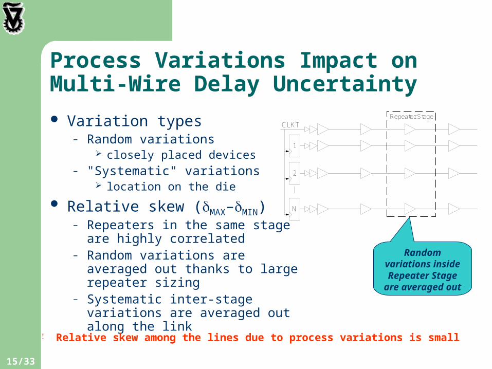
Process Variations Impact onMulti-Wire Delay Uncertainty
Variation types– Random variations
closely placed devices– "Systematic" variations
location on the die
Relative skew (dMAX–dMIN)– Repeaters in the same stage are
highly correlated– Random variations are averaged
out thanks to large repeater sizing– Systematic inter-stage variations
are averaged out along the link
Repeater Stage
1
2
N
CLKT
Random variations inside Repeater Stage
are averaged out
Relative skew among the lines due to process variations is small

16/33
Cross-Coupling Impact onMulti-Wire Delay Uncertainty
Let’s approximate the wire delay by:
( )Worstcross talk SI RPTR INT INTD v K d v K d L
Repeater Delay Wire Delay
transistor variation
number of repeaters
nominal repeater
delay
coupling factor
wire variation
wire segment (L) nominal
delay
Worst case skew Φ between two lines:
( )
( ) ( ( ))
Worst BestMAX MIN cross talk cross talk
Worst BestINT INT
L D D
v K d L
d d
17/33
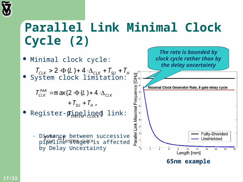
Parallel Link Minimal Clock Cycle (2) Minimal clock cycle:
System clock limitation:
Register-pipelined link:
– Distance between successive pipeline stages is affected by Delay Uncertainty
2 ( ) 4CLK CLK SU HT L T T D
65nm example
The rate is bounded by clock cycle rather than the
delay uncertainty
The rate is bounded by clock cycle rather than by
the delay uncertainty
max{2 ( ) 4
,
}
PARCLK CLK
SU H
SYSTEM CLOCK
T L
T T
T
D
PARCLK SYSTEM CLOCKT T

18/33
Serial Link Bit Rate
Skew due to in-die variation is neglected– much smaller than in parallel link
Coupling factor is always known– LEDR encoding: there is only one transition per
each transmitted bit– The skew is not affected by cross-coupling
link delay is similar for all symbols
Bit rate:41 /SERB d

19/33
Scalability
Number of repeaters (per millimeter) grows for more advanced technology nodes
Active area and leakage: Minimal link length for serial link employment decreases with technology
Dynamic power: Minimal link length for serial link employment decreases with technology
Interconnect area: Serial link is always preferable
( ): 1
( )
( ): 1
( )
AREA PARMIN
SER
POWER PARMIN
SER
A LL
A L
P LL
P L
0
0.5
1
1.5
2
180 130 90 65 45 32
Technology Node [nm]k
=K
/mm
0.0
2.0
4.0
6.0
8.0
10.0
Lm
in [
mm
]
Y.I. Ismail, et al., Repeater Insertion in RLC Lines for Minimum Propagation Delay, ISCAS99
Power
Repeaters
Number of repeaters grows with technology
node scaling
The range for serial link employment decreases with
technology node scaling
Area and Leakage

20/33
65nm Case Study

21/33
Goals and Set-up
Compare– Wave-pipelined (shielded/unshielded) vs. Serial– Register-pipelined (shielded/unshielded) vs. Serial
In terms of: – Area– Power– Latency– Length
All links deliver the same bandwidth– BSER – the bandwidth of single serial link
22/33
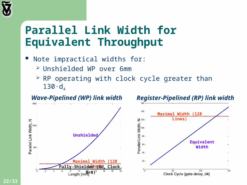
Parallel Link Width forEquivalent Throughput Note impractical widths for:
Unshielded WP over 6mm RP operating with clock cycle greater than 130∙d4
Wave-Pipelined (WP) link width Register-Pipelined (RP) link width
Maximal Width (128 Lines)
Equivalent Width
Maximal Width (128 Lines)
Unshielded
Fully-Shielded (8d4 Clock, N=8)
23/33
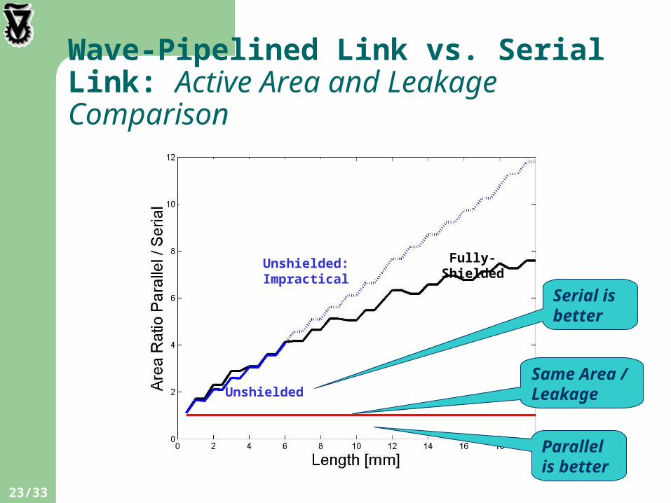
Wave-Pipelined Link vs. Serial Link: Active Area and Leakage Comparison
Same Area / Leakage
Parallel is better
Serial is better
Fully-Shielded
Unshielded
Unshielded: Impractical

24/33
Wave-Pipelined Link vs. Serial Link: Total Area Comparison (Incl. Interconnect)
Serial is always better
Fully-ShieldedUnshielded
Unshielded: Impractical

25/33
Register-Pipelined Link vs. Serial Link: Active Area and Leakage Comparison
Fully-Shielded, T=10d4
Fully-Shielded, T=130d4
Unshielded, T=10d4
Unshielded, T=130d4
Serial is always better

26/33
Register-Pipelined Link vs. Serial Link: Total Area Comparison (Incl. Interconnect)
Serial is always better
Fully-Shielded, T=130d4
Unshielded, T=10d4
Unshielded, T=130d4
Fully-Shielded, T=10d4
27/33
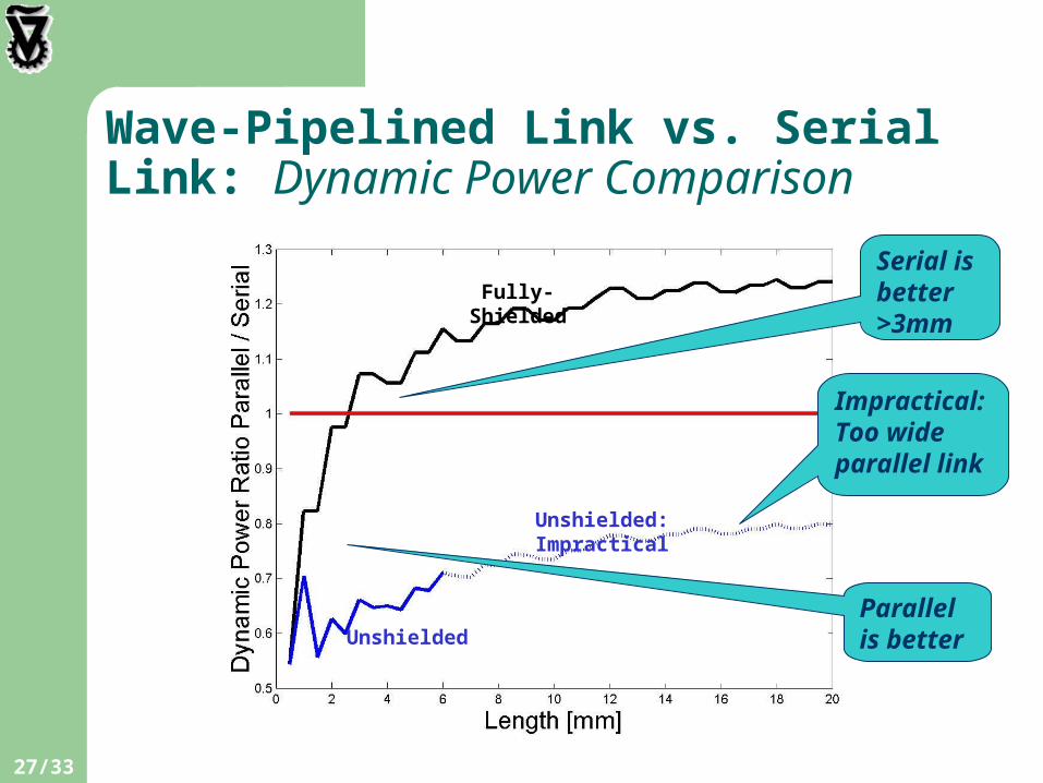
Wave-Pipelined Link vs. Serial Link: Dynamic Power Comparison
Impractical: Too wide parallel link
Serial is better>3mm
Fully-Shielded
Unshielded
Unshielded: Impractical
Parallel is better

28/33
Wave-Pipelined Link vs. Serial Link: Total Power Comparison
Fully-Shielded
Unshielded
Unshielded: Impractical
20% Utilization

29/33
Register-Pipelined Link vs. Serial Link: Dynamic Power Comparison
Fully-Shielded, T=130d4
Unshielded, T=130d4
Fully-Shielded, T=10d4
Unshielded, T=10d4

30/33
Register-Pipelined Link vs. Serial Link: Total Power Comparison
20% Utilization
Unshielded, T=130d4
Fully-Shielded, T=10d4
Unshielded, T=10d4
Fully-Shielded, T=130d4

31/33
Test Case Summary
Wave-Pipeline vs. SerialRegister-pipelined vs. Serial
ShieldingFully Shielded UnshieldedFully ShieldedUnshielded
Length of parallel link
unlimitedup to 6mmunlimitedunlimited
Clock cycle of parallel link
8d48d4
10d4
(fast)
130d4
(slow)
10d4
(fast)
130d4
(slow)
To minimize the following:
choose a serial link for links longer than:
AreaAlwaysAlwaysAlwaysAlways
Power2 mm4mm3mm3mm1mm3mm
Latency 2 mmNever*4mm12mm2mm9mm
Minimal length above which the serial link is preferred
32/33
Conclusions
Novel high-speed serial links outperform parallel links for long range communication
The serial link is more attractive for shorter ranges in future technologies
Future large SoCs and NoCs should employ serial links to mitigate:
– Area– Routing Congestion– Power– Latency

SLIP-2008, Newcastle upon Tyne, UKApril 5, 2008
Thank You!


![VERY BASIC LIE THEORY - University of Oregonpages.uoregon.edu/arkadiy/howe.very.basic.lie.theory.pdf · This led Felix Klein to enunciate his Erlanger Programm [Kl] for the systematic](https://img.pdfslide.net/doc/110x75/5b949d1d09d3f2130d8d0ed6/very-basic-lie-theory-university-of-this-led-felix-klein-to-enunciate-his.jpg)


![University of Oregonpages.uoregon.edu/arkadiy/feiginchar.pdf · 2013. 10. 28. · arXiv:1308.2992v1 [math.QA] 13 Aug 2013 QUANTUM CLUSTER CHARACTERS OF HALL ALGEBRAS ARKADY BERENSTEIN](https://img.pdfslide.net/doc/110x75/60e3c39ef460cd2e525b9935/university-of-2013-10-28-arxiv13082992v1-mathqa-13-aug-2013-quantum-cluster.jpg)