Embed Size (px)
Citation preview
2 | Advanced Driver Assistance Systems (ADAS) Guide 2013 Texas Instruments
Advanced Driver Assistance (ADAS)Table of Contents
Advanced Driver Assistance Systems (ADAS)3 Overview
Camera-Based Systems4 Overview
5 TDA2x (Vision 28) ADAS Application Processor
7 FTP-Link
7 LMH6551Q-Q1
8 LP3907-Q1
Radar-Based Systems9 Overview
10 AFE5401
11 TPS65310A-Q1
12 TPS65381-Q1
13 Light Detection and Range (LIDAR) /Ultrasonic Park Assist
Sensor Fusion14 Overview
Hercules™ Safety MCUs15 Overview
16 Hercules™ TMS570LS Safety MCU
17 Hercules™ Evaluation and Development Kits
18 Hercules™ Tools and Software
Selection Tables19 Operational Amplifiers
19 Data Converters
20 Standard Logic
20 Power Management
22 FPD-Link II and III SERDES
23 TMS570 Family
24 TMS320 Family
25 DaVinci™ Digital Media Processors (DM643x)
26 DSP+ARM Processors (OMAP-L1x) Selection Guide
Advanced Driver AssistanceSystems (ADAS) are one of the fastest-growing application areas in vehicles today. A multitude of features can now warn drivers, allow better visibility into what is going on outside the car, and support features like park assist and adaptive cruise control; these are achieved with radar-, camera-, light detection and range (LIDAR)- and ultrasound-based systems. Advanced ADAS functions and autonomous driving do require the use of multiple systemstogether.
The fast growth and proliferation ofADAS features into even the middleand lower ends of the car market. TI provides both analog and digitalsolutions and has a strong roadmapto support the evolution and growth of this exciting application space.
During the past 10 years, safety hasbecome as much of a selling point inthe automotive market as fuel economyand performance. Today’s safetysystems are designed to help vehiclepassengers not only escape injuryduring an accident, but actually helpprevent the accident in the first place.Texas Instruments (TI) is committed to providing industry-leading technolo-gies for ADAS solutions, complete with excellent product documentation, which meets increasingly demanding OEM specifications and makes the road a safer place. From lane-departure warnings to drowsinessmonitoring, ultrasonic park assist,advanced braking systems andother ADAS applications, TI’s power-management and control solu-tions, robust processors, communica-tion interfaces, display components and microcontrollers help you deliverworld-class ADAS features.
Texas Instruments Commitment to Automotive Safety
Automotive-Qualified Products (Q1)
TI’s automotive-qualified products are indicated by the Q1 suffix. The Q1 indicates that a product has met TI’s stringent automotive standards and includes:• 180-day product-change notification
from final notice.• Extended temperature qualification.• Automotive documentation service.• Target zero defects.
Texas Instruments Advanced Driver Assistance Systems (ADAS) Guide 2013 | 3
Overview
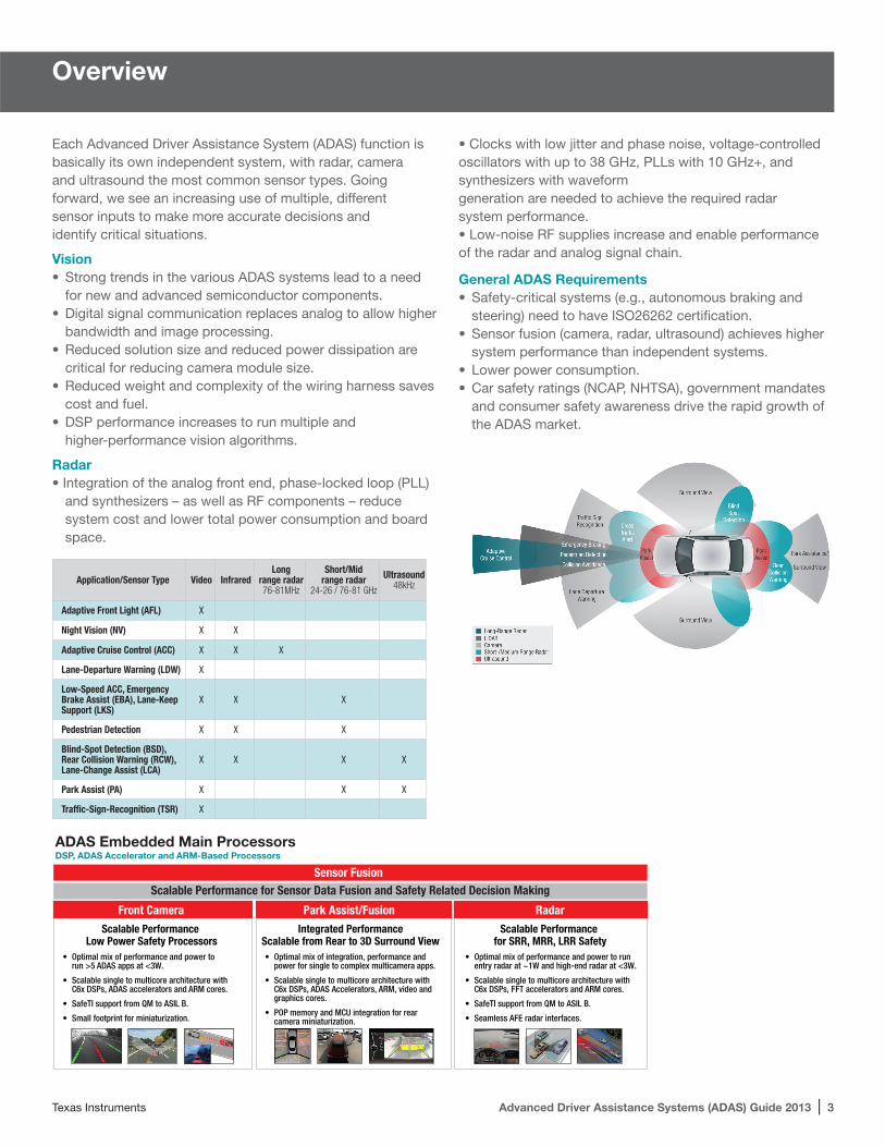
Each Advanced Driver Assistance System (ADAS) function is basically its own independent system, with radar, camera and ultrasound the most common sensor types. Going forward, we see an increasing use of multiple, different sensor inputs to make more accurate decisions and identify critical situations.
Vision• Strong trends in the various ADAS systems lead to a need for new and advanced semiconductor components.• Digital signal communication replaces analog to allow higher
bandwidth and image processing.• Reduced solution size and reduced power dissipation are
critical for reducing camera module size.• Reduced weight and complexity of the wiring harness saves
cost and fuel.• DSP performance increases to run multiple and
higher-performance vision algorithms.
Radar• Integration of the analog front end, phase-locked loop (PLL) and synthesizers – as well as RF components – reduce system cost and lower total power consumption and board space.
• Clocks with low jitter and phase noise, voltage-controlled oscillators with up to 38 GHz, PLLs with 10 GHz+, and synthesizers with waveformgeneration are needed to achieve the required radarsystem performance.• Low-noise RF supplies increase and enable performanceof the radar and analog signal chain.
General ADAS Requirements• Safety-critical systems (e.g., autonomous braking and
steering) need to have ISO26262 certification.• Sensor fusion (camera, radar, ultrasound) achieves higher
system performance than independent systems.• Lower power consumption.• Car safety ratings (NCAP, NHTSA), government mandates
and consumer safety awareness drive the rapid growth of the ADAS market.
Application/Sensor Type Video InfraredLong
range radar76-81MHz
Short/Mid range radar
24-26 / 76-81 GHz
Ultrasound48kHz
Adaptive Front Light (AFL) X
Night Vision (NV) X X
Adaptive Cruise Control (ACC) X X X
Lane-Departure Warning (LDW) X
Low-Speed ACC, Emergency Brake Assist (EBA), Lane-Keep Support (LKS)
X X X
Pedestrian Detection X X X
Blind-Spot Detection (BSD), Rear Collision Warning (RCW), Lane-Change Assist (LCA)
X X X X
Park Assist (PA) X X X
Traffic-Sign-Recognition (TSR) X
ADAS Embedded Main Processors DSP, ADAS Accelerator and ARM-Based Processors
Park Assist/Fusion RadarFront Camera
• Optimal mix of performance and power to run >5 ADAS apps at <3W.
• Scalable single to multicore architecture with C6x DSPs, ADAS accelerators and ARM cores.
• SafeTI support from QM to ASIL B.
• Small footprint for miniaturization.
Sensor Fusion Scalable Performance for Sensor Data Fusion and Safety Related Decision Making
Scalable Performance Low Power Safety Processors
• Optimal mix of integration, performance and power for single to complex multicamera apps. • Scalable single to multicore architecture with C6x DSPs, ADAS Accelerators, ARM, video and graphics cores.
• POP memory and MCU integration for rear camera miniaturization.
Integrated PerformanceScalable from Rear to 3D Surround View
• Optimal mix of performance and power to run entry radar at ~1W and high-end radar at <3W. • Scalable single to multicore architecture with C6x DSPs, FFT accelerators and ARM cores.
• SafeTI support from QM to ASIL B.
• Seamless AFE radar interfaces.
Scalable Performance for SRR, MRR, LRR Safety
4 | Advanced Driver Assistance Systems (ADAS) Guide 2013 Texas Instruments
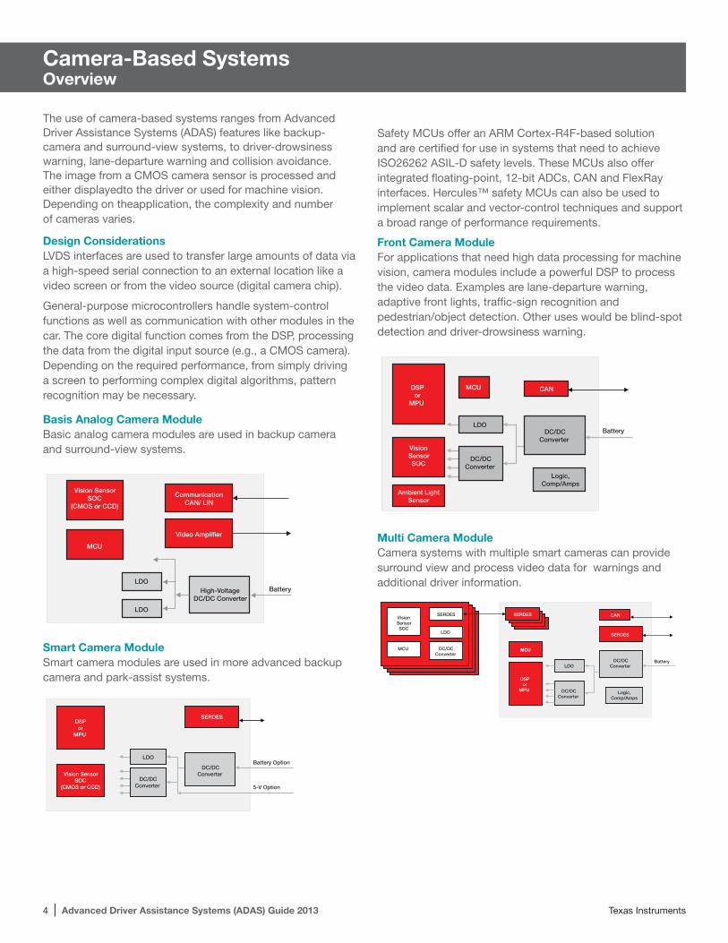
Basis Analog Camera ModuleBasic analog camera modules are used in backup camera and surround-view systems.
Smart Camera Module Smart camera modules are used in more advanced backupcamera and park-assist systems.
Front Camera ModuleFor applications that need high data processing for machinevision, camera modules include a powerful DSP to process the video data. Examples are lane-departure warning, adaptive front lights, traffic-sign recognition andpedestrian/object detection. Other uses would be blind-spot detection and driver-drowsiness warning.
Multi Camera ModuleCamera systems with multiple smart cameras can provide surround view and process video data for warnings and additional driver information.
Camera-Based SystemsOverview
BatteryLDO
LDO
MCU
Vision SensorSOC
(CMOS or CCD)Communication
CAN/ LIN
Video Amplifier
High-VoltageDC/DC Converter
Vision SensorSOC
(CMOS or CCD)
SERDES DSPor
MPU
Battery Option
5-V Option
DC/DCConverter
LDO
DC/DCConverter
Battery
CAN
Logic,Comp/Amps
Ambient LightSensor
DSPor
MPU
VisionSensorSOC
MCU
LDO
DC/DCConverter
DC/DCConverter
Battery
CAN
MCU
Ser-Des Ser-Des Ser-Des SERDES SERDES
SERDES
MCU
LDO
DC/DCConverter
DC/DCConverter
VisionSensorSOC
DSPor
MPU Logic,Comp/Amps
LDO
DC/DCConverter
The use of camera-based systems ranges from Advanced Driver Assistance Systems (ADAS) features like backup-camera and surround-view systems, to driver-drowsiness warning, lane-departure warning and collision avoidance. The image from a CMOS camera sensor is processed and either displayedto the driver or used for machine vision. Depending on theapplication, the complexity and number of cameras varies.
Design ConsiderationsLVDS interfaces are used to transfer large amounts of data viaa high-speed serial connection to an external location like avideo screen or from the video source (digital camera chip).
General-purpose microcontrollers handle system-controlfunctions as well as communication with other modules in thecar. The core digital function comes from the DSP, processingthe data from the digital input source (e.g., a CMOS camera).Depending on the required performance, from simply drivinga screen to performing complex digital algorithms, pattern recognition may be necessary.
Safety MCUs offer an ARM Cortex-R4F-based solutionand are certified for use in systems that need to achieveISO26262 ASIL-D safety levels. These MCUs also offerintegrated floating-point, 12-bit ADCs, CAN and FlexRay interfaces. Hercules™ safety MCUs can also be used to implement scalar and vector-control techniques and support a broad range of performance requirements.
Texas Instruments Advanced Driver Assistance Systems (ADAS) Guide 2013 | 5
Camera-Based Systems
TDA2x (Vision 28) ADAS Application Processor
OverviewTI’s new TDA2x Vision 28 system-on-chip (SoC) is a highly opti-mized and scalable device family designed to meet the require-ments of leading advanced driver assistance systems (ADAS). The TDA2x family empowers broad ADAS applications in today’s automobiles by integrating an optimal mix of performance, low power and ADAS vision-analytics processing that aims to facili-tate a more autonomous and collision-free driving experience.
The TDA2x SoC makes possible sophisticated embedded vision technology, providing the industry’s broadest range of ADAS applications such as front camera, park assist, surround view and sensor fusion on a single architecture. Front-camera applications include high-beam assist, lane-keep assist, adaptive cruise control, traffic-sign recognition, pedestrian/object detection and collision avoidance. Park-assist applications include intelligent 2-D and 3-D surround view and rear-collision warning and detection. The TDA2x SoC is also capable of handling the fusion of radar and camera sensor data, allowing for a more robust ADAS decision-making process.
TDA2xThe TDA2x SoC incorporates a heterogeneous, scalable architecture that includes a mix of TI’s fixed- and floating-point TMS320C66x digital signal processor (DSP) generation cores, Vision AccelerationPac, ARM Cortex-A15 MPCoreand dual Cortex-M4 processors. The integration of video for decoding multiple video streams over Ethernet audio-video bridging (AVB) networks, along with graphics accelerators for rendering virtual views, allows for a 3-D viewing experience. And the TDA2x SoC integrates a host of peripherals, including multicamera interfaces (both parallel and serial) for LVDS-based surround-view systems, displays, CAN and Gigabit Ethernet AVB.
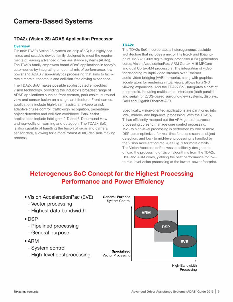
Specifically, vision-oriented applications are partitioned into low-, middle- and high-level processing. With the TDA2x, TI has efficiently mapped out the ARM general-purpose processing cores to manage core control processing. Mid- to high-level processing is performed by one or more DSP cores optimized for real-time functions such as object detection, and low- to mid-level processing is handled by the Vision AccelerationPac. (See Fig. 1 for more details.)The Vision AccelerationPac was specifically designed to offload the processing of vision algorithms from the TDA2x DSP and ARM cores, yielding the best performance for low- to mid-level vision processing at the lowest-power footprint.
ARM
DSP
EVE
General-PurposeSystem Control
SpecializedVector Processing
High-BandwidthProcessing
• Vision AccelerationPac (EVE) - Vector processing - Highest data bandwidth
• DSP - Pipelined processing - General purpose
• ARM - System control - High-level postprocessing
Heterogenous SoC Concept for the Highest Processing Performance and Power Efficiency
6 | Advanced Driver Assistance Systems (ADAS) Guide 2013 Texas Instruments
The TDA2x SoC includes TI’s new Vision AccelerationPac, which delivers up to a 10× improvement in performance for advanced vision analytics over existing ADAS systems at similar power levels. The Vision AccelerationPac for this family of products includes multiple embedded vision engines (EVEs) offloading the vision-analytics functionality from the application processor. The Vision AccelerationPac is optimized for vision processing with a 32-bit RISC core for efficient program execution and a vector coprocessor for specialized vision processing. With each core operating a 16 MAC-per-cycle computing engine up to 650 MHz (8 bit or 16 bit), the Vision AccelerationPac is able to deliver more than 10.4 GMACs per core, for a total of >40 GMACs for quad EVEs devices. This provides the most efficient vision analytics for real-time vision-based automotive applications and allows the most 16 × 16-bit multiplies compared to other processor architectures.
The TDA2x SoC includes a broad range of cores. It includes dual next-generation C66x fixed-/floating-point DSP cores that operate at up to 750 MHz to support high-level signal processing, and a 750-MHz Cortex-A15 core for control and general-purpose processing. With 200 MHz of processing performance, the Cortex-M4 cores deliver efficient control
Camera-Based Systems
and processing camera streams. TI’s IVA-HD core is an imaging and video codec accelerator running at up to 532 MHz to facilitate full HD video encoding and decoding.
The TDA2xx SoC has up to 2.5 MB of on-chip L3 RAM with single error correct and double error detect (SECDED) support to minimize the impact of soft error rate (SER). Each of the DSP cores has 32 KB of both L1 data and programming memory as well as a unified 256 KB L2 cache. The ARM cores have 32 KB of L1 data and programming memory as well as a combined 2-MB L2 cache.
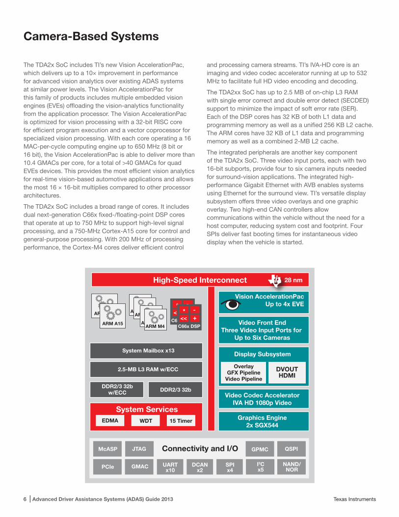
The integrated peripherals are another key component of the TDA2x SoC. Three video input ports, each with two 16-bit subports, provide four to six camera inputs needed for surround-vision applications. The integrated high-performance Gigabit Ethernet with AVB enables systems using Ethernet for the surround view. TI’s versatile display subsystem offers three video overlays and one graphic overlay. Two high-end CAN controllers allow communications within the vehicle without the need for a host computer, reducing system cost and footprint. Four SPIs deliver fast booting times for instantaneous video display when the vehicle is started.
High-Speed Interconnect
System Services
Connectivity and I/O
28 nm
System Mailbox x13
Vision AccelerationPacUp to 4x EVE
Video Front EndThree Video Input Ports for
Up to Six Cameras
Video Codec AcceleratorIVA HD 1080p Video
Graphics Engine2x SGX544
Display Subsystem
2.5-MB L3 RAM w/ECC
DDR2/3 32bw/ECC DDR2/3 32b
EDMA WDT 15 Timer
OverlayGFX Pipeline
Video Pipeline
DVOUTHDMI
McASP
PCIe
JTAG
GMAC UARTx10
DCANx2
SPIx4
GPMC
I2Cx5
QSPI
NAND/NOR
C66x DSP
*+<<-
C66x DSP
*+<<-
ARM A15
ARM A15
ARM M4ARM M4
ARM M4ARM M4
Texas Instruments Advanced Driver Assistance Systems (ADAS) Guide 2013 | 7
Differential, High-Performance Operational Amplifier
LMH6551Q-Q1
The LMH6551-Q1 is a high-performance voltage feedback differential amplifier. The LMH6551-Q1 has the high speed and low distortion necessary for driving high-performance ADCs as well as the current-handling capability to drive signals over balanced transmission lines like CAT 5 data cables. The LMH6551-Q1 can handle a wide range of video and data formats.
With external gain set resistors, the LMH6551-Q1 can be used at any desired gain. Gain flexibility coupled with high speed makes the LMH6551-Q1 suitable for use as an IF amplifier in high-performance communications equipment.
Key Features• 370-MHz to 3-dB bandwidth
(VOUT = 0.5 VPP)• 50-MHz 0.1-dB bandwidth• 2400-V/µs slew rate• 18-ns settling time to 0.05%• -94/-96 dB HD2/HD3 at 5 MHz• LMH6551-Q1 is AEC-Q100 Grade 1
qualified and is manufactured on an automotive grade flow
Applications • Fully differential video driving• Video over twisted pair
VS
RS
VCM
V—
V+AV, RIN
RT
RM RG
RG
RF
RO
RO
VO —
+—
+
IN+
IN—ADC
RF
VI
Functional block diagram
Camera-Based Systems
FPD-Link
• DS90UB913A/914A serializer/deserializer (SERDES)• Supports megapixel image sensors• No compression for best video quality• Small camera module size
No microcontroller neededVideo, control and power over one cable/connectorISP companion chip can be located away from camera in ECU
• Low costInexpensive coax cableLow component countFits on one PCB
• Very low < 15-µs latency• Supports power-over-coax data cable• Low power consumption
Less heat for better low-light performance
Sensor
>2 MHz FSWmicroSMD optional
Power
D[11:0]
100 µH 100 µH
video + controlframesync + power
4.7 µH 4.7 µH
47 nF 47 nF50Ω 50Ω
100 nF 100 nFHSVS
48 MHzOSC
GPI02
PCLKFrameSync
12C
GPI03
Power
R[11:0]
HSVS
PCLKFrameSync
12C
5 x 5 mmpackage
isolated fromchassis ground
DS90UB913AQ DS90UB914AQ
LMxxxxtiny DC/DC
TPS2xxxswitch/protect
TPS/LMDC/DC
OMAP/Vision SoC
(under NDA)
Built
-In S
elf T
est
RBS
Ser
ializ
er
ControlLogic
+2
Adap
tive
Equa
lizer
RBS
Des
eria
lizer
Built
-In S
elf T
ext
PLLCDR
ControlLogic
8 | Advanced Driver Assistance Systems (ADAS) Guide 2013 Texas Instruments
Camera-Based Systems
Dual High-Current Step-Down DC/DC and Dual Linear Regulator with I2C-Compatible Interface
LP3907-Q1
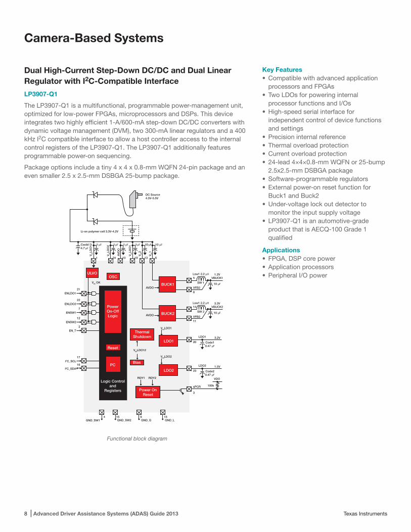
The LP3907-Q1 is a multifunctional, programmable power-management unit, optimized for low-power FPGAs, microprocessors and DSPs. This device integrates two highly efficient 1-A/600-mA step-down DC/DC converters with dynamic voltage management (DVM), two 300-mA linear regulators and a 400 kHz I2C compatible interface to allow a host controller access to the internal control registers of the LP3907-Q1. The LP3907-Q1 additionally features programmable power-on sequencing.
Package options include a tiny 4 x 4 x 0.8-mm WQFN 24-pin package and an even smaller 2.5 x 2.5-mm DSBGA 25-bump package.
Key Features• Compatible with advanced application
processors and FPGAs• Two LDOs for powering internal
processor functions and I/Os• High-speed serial interface for
independent control of device functions and settings
• Precision internal reference• Thermal overload protection• Current overload protection• 24-lead 4×4×0.8-mm WQFN or 25-bump
2.5x2.5-mm DSBGA package• Software-programmable regulators• External power-on reset function for
Buck1 and Buck2 • Under-voltage lock out detector to
monitor the input supply voltage• LP3907-Q1 is an automotive-grade
product that is AECQ-100 Grade 1 qualified
Applications • FPGA, DSP core power • Application processors • Peripheral I/O power
BUCK1AVDO
DC Source4.5V-5.5V
3
23
20
11VFB2
14
sPCR 100k
Code20.47 µF
1.5V
AVDO
ENLDO121
ENLDO222
ENSW17
ENSW212
EN_T2
I2C_SCL17
I2C_SDA16
GND_SW14
GND_SW2
VINLDO2
VINLDO12
RDY1 RDY2 VDO
LDO2
Code10.47 µF
10 µF
3.3VVBUCK2
Lsw1 2.2 µH
SW 2
8VFB2
5
6
V IN1
V IN2
V INLD
O1
V INLD
O2
V INLD
O12
AVD
O
131910241
10 µF
10 µF10 µF1 µF1 µF1 µF1 µFCwdd4.7 µF
Li-on polymer cell 3.3V-4.2V
1.2VVBUCK1
Lsw1 2.2 µH
SW 1
3.2VLDO1
VINLDO1
15GND_G
9GND_L
15
VIN OK
BUCK2
LDO1
LDO2PC
Reset
Bias
PowerOn-OffLogic
Power OnReset
ThermalShutdown
OSCULVO
Logic Controland
Registers
Functional block diagram
Texas Instruments Advanced Driver Assistance Systems (ADAS) Guide 2013 | 9
Radar-Based SystemsOverview
TI supports radar trends with highly integrated basebandand analog front ends, as well as integrated synthesizers/ramp pulse generators, high-performance DSPs, andsafety microcontroller and (low-noise) power-supply solutions. The other group of radar systems is medium-/short-rangeradar (Fig 3).
These systems typically include blind-spot detection, side-collision warning, cross-traffic alert and lane-change assistance. The overall performance of these systems is lower compared to their long-range brethren; they are even available in some mid-range cars as standard equipment. Medium-/short-range radar systems are mounted in different locations of the car, depending on their function. Because of their use and functionality, system size and cost are important. The lower performance often allows the use of microcontrollers instead of DSPs.
TI’s portfolio offers the right mix of catalog and differentiated ICs to help you be successful and meet your design, space and price targets.
Embedded processorC28xxC6xxx
EthernetTransceiver
EthernetTransceiver
CAN
FlexRayTransceiver
Transceiver
Safety MCUTMS570
TPS65381Supervisors,
Watchdog,Power Supply
Automotive Safety Solution
Optional Optional
Flash RAM
LVDS
Optional
Optional
RadarSolution
uC or DSP
DC/DC
Op Amp
VCO Driver
DC/DC
Low-Noise Supply
Vbatt
LDO LNA
CAN
DAC
ADC
1-2 RF TX
2-4RF RX
CAN
DSP
PMIC
RF PLL/ Synthesizer
DAC
FlexRay
MCU
Clocks/ Jitter Cleaner
Op AmpADC
VCO Driver
Logic, Comp/Amps.
DC/DC
Ultra-Low Noise Supply
Vbatt
LNA
1-4 RF TX
4-8 RF RX
Fig. 3: Short-and medium-range radar system diagram
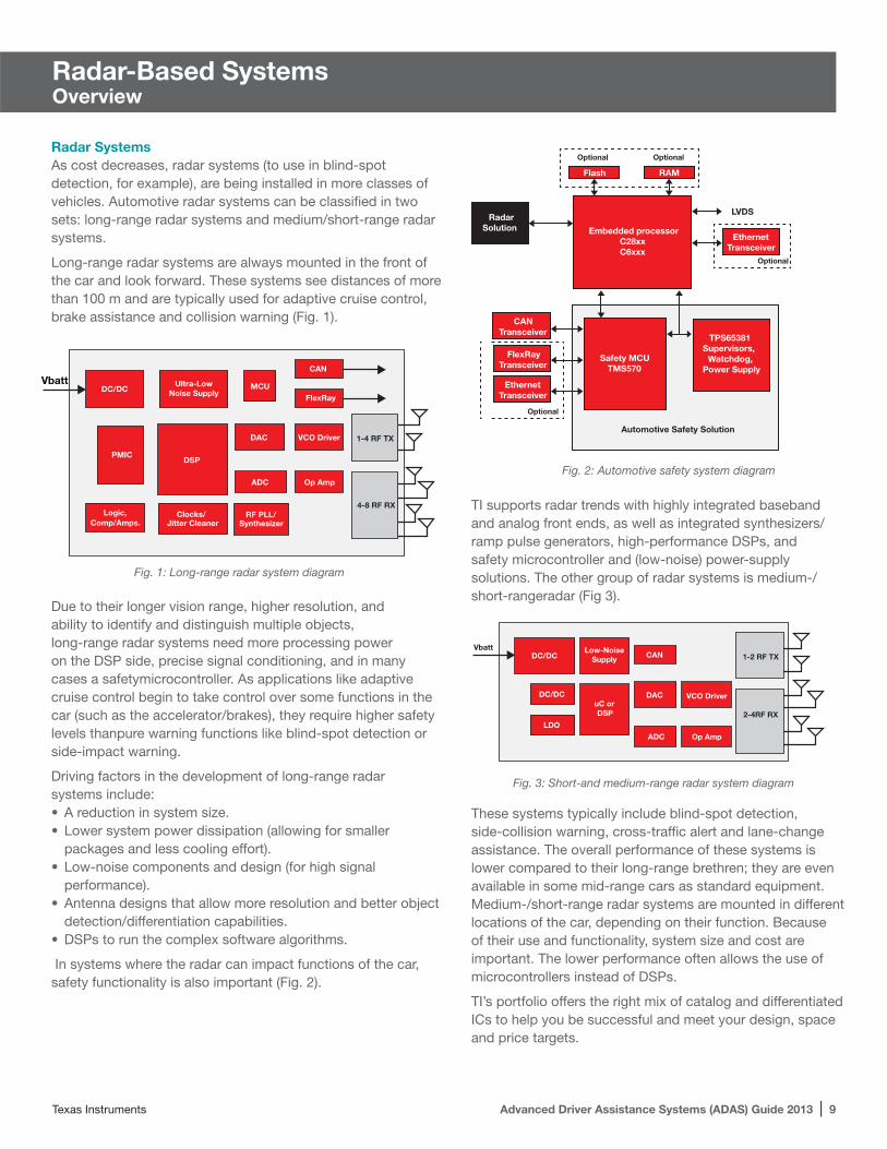
Radar SystemsAs cost decreases, radar systems (to use in blind-spot detection, for example), are being installed in more classes of vehicles. Automotive radar systems can be classified in two sets: long-range radar systems and medium/short-range radar systems.
Long-range radar systems are always mounted in the front of the car and look forward. These systems see distances of more than 100 m and are typically used for adaptive cruise control, brake assistance and collision warning (Fig. 1).
Due to their longer vision range, higher resolution, and ability to identify and distinguish multiple objects, long-range radar systems need more processing power on the DSP side, precise signal conditioning, and in many cases a safetymicrocontroller. As applications like adaptive cruise control begin to take control over some functions in the car (such as the accelerator/brakes), they require higher safety levels thanpure warning functions like blind-spot detection or side-impact warning.
Driving factors in the development of long-range radar systems include:• A reduction in system size.• Lower system power dissipation (allowing for smaller
packages and less cooling effort).• Low-noise components and design (for high signal
performance).• Antenna designs that allow more resolution and better object
detection/differentiation capabilities.• DSPs to run the complex software algorithms.
In systems where the radar can impact functions of the car, safety functionality is also important (Fig. 2).
Fig. 2: Automotive safety system diagram
Fig. 1: Long-range radar system diagram
10 | Advanced Driver Assistance Systems (ADAS) Guide 2013 Texas Instruments
Radar-Based Systems
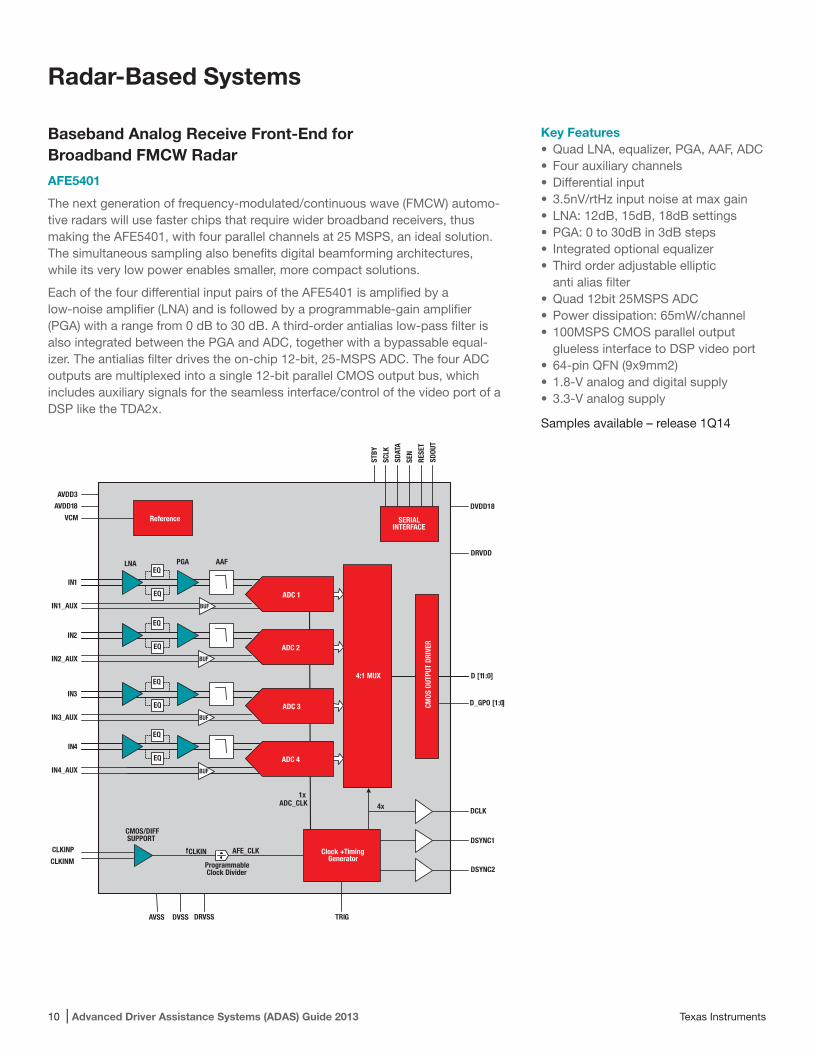
Baseband Analog Receive Front-End for Broadband FMCW Radar
AFE5401
The next generation of frequency-modulated/continuous wave (FMCW) automo-tive radars will use faster chips that require wider broadband receivers, thus making the AFE5401, with four parallel channels at 25 MSPS, an ideal solution. The simultaneous sampling also benefits digital beamforming architectures, while its very low power enables smaller, more compact solutions.
Each of the four differential input pairs of the AFE5401 is amplified by a low-noise amplifier (LNA) and is followed by a programmable-gain amplifier (PGA) with a range from 0 dB to 30 dB. A third-order antialias low-pass filter is also integrated between the PGA and ADC, together with a bypassable equal-izer. The antialias filter drives the on-chip 12-bit, 25-MSPS ADC. The four ADC outputs are multiplexed into a single 12-bit parallel CMOS output bus, which includes auxiliary signals for the seamless interface/control of the video port of a DSP like the TDA2x.
Key Features• Quad LNA, equalizer, PGA, AAF, ADC• Four auxiliary channels • Differential input • 3.5nV/rtHz input noise at max gain • LNA: 12dB, 15dB, 18dB settings• PGA: 0 to 30dB in 3dB steps• Integrated optional equalizer• Third order adjustable elliptic
anti alias filter• Quad 12bit 25MSPS ADC• Power dissipation: 65mW/channel• 100MSPS CMOS parallel output
glueless interface to DSP video port• 64-pin QFN (9x9mm2)• 1.8-V analog and digital supply• 3.3-V analog supply
Samples available – release 1Q14
SERIALINTERFACE
SDOU
T
RESE
T
SEN
SDAT
A
SCLK
STBY
DVDD18
DRVDD
DRVSS
AVDD3
AVDD18
VCM
CMOS
OUT
PUT
DRIV
ER
4:1 MUX
IN1
IN1_AUX
IN2
IN2_AUX
IN3
IN3_AUX
IN4
IN4_AUX
ADC 1
ADC 2
ADC 3
ADC 4
D [11:0]
Clock + TimingGenerator
1xADC_CLK
CMOS/DIFFSUPPORT
ProgrammableClock Divider
AFE_CLKfCLKIN
TRIG
CLKINP
CLKINM
AVSS DVSS
DSYNC1
DCLK
DSYNC2
AAFPGALNA
BUF
BUF
BUF
BUF
EQ
EQ
EQ
EQ
EQ
EQ
EQ
EQ
D_GPO [1:0]
Reference
4x
Texas Instruments Advanced Driver Assistance Systems (ADAS) Guide 2013 | 11
Radar-Based Systems
Power Management Unit for Advanced Driver Assistance Systems
TPS65310A-Q1 The TPS65310A-Q1 device is a power-management unit, meeting therequirements of DSP-controlled automotive systems like advanced driver assistance systems (ADAS). It is ideally suited for camera- or radar-based vision systems to support features like lane-departure warning, collision avoidance systems, blind-spot detection, park assist and traffic-sign detection.
The device includes one high-voltage buck controller for preregulation,combined with two buck controllers and one boost converter for postregulation. A further integrated low dropout (LDO) rounds up the power-supply concept and offers a flexible system design with five independent voltage rails. The device offers a low-power state (LPM0 with all rails off) to reduce current consumption in case the system is constantlyconnected to the battery line. All outputs are protected against overload and overtemperature.
The integrated window watchdog and SPI for control and diagnosis enables safety-related applications in ADAS systems. Safety levels up to ASIL-B can be realized using the TPS65310A-Q1.
Key Features• -40°C to 125°C ambient operating
temperature• Device HBM ESD Classification Level
H1B• Device CDM ESD Classification Level
C3B• Input voltage range: 4 V to 40 V,
transients up to 60 V; 80 V • Single-output synchronous buck
controller • Peak gate drive current 0.6 A• 490-kHz fixed switching frequency• Pseudo-random frequency hopping
spread-spectrum or triangular mode• Dual synchronous buck converter • Designed for output currents up to 2 A• Out-of-phase switching• Switching frequency: 0.98 MHz• Adjustable 350-mA linear regulator• Adjustable asynchronous boost converter • 1-A integrated switch• Switching frequency: 0.98 MHz• Soft-start feature for all regulator outputs• Independent voltage monitoring• Undervoltage (UV) detection and
overvoltage (OV) protection
Functional block diagram
LEDDriver
Switch OffComparator
ProtectionFET SPI
VBU12 VBU33 VBU12
LVDS
ADC
ADC
VL28
DVDDIO
VBU33
EMIF EMIF
Flash/EEPROM
DDR2/SRAM
DVDDR2
VBU18
AR
EF
VB
U33
VB
U18
AR
EF
VB
U33
VB
U18
VBU33 VB5
CA
N
GP
IO
GP
IOM
cBS
Po
r H
PI
Vid
eoO
utp
ut
Vid
eoIn
put
Eth
erne
tM
AC
Vid
eoIn
put
Vid
eoIn
put
Vid
eoD
AC
Watchdog,LED
SP
I or
EM
IF
Flex
Ray
VBAT
CANBus
CANXCVR
MCU(e.g., TMS570)
DSP(e.g., DM6437)
Display
WindowWatchdog Wake
AnalogReference
3.3 V(AREF)
LinearRegulator
1.x-xxV(VL28)
BoostRegulator
5V(VB5)
DC/DCConverter
1.2V(VBU12)
DC/DCConverter
1.8V(VBU18)
DC/DCConverter
3.3V(VBU33)
TPS65310
12 | Advanced Driver Assistance Systems (ADAS) Guide 2013 Texas Instruments
Radar-Based Systems
Power-Management Unit for Safety CriticalAdvanced Driver Assistance Systems
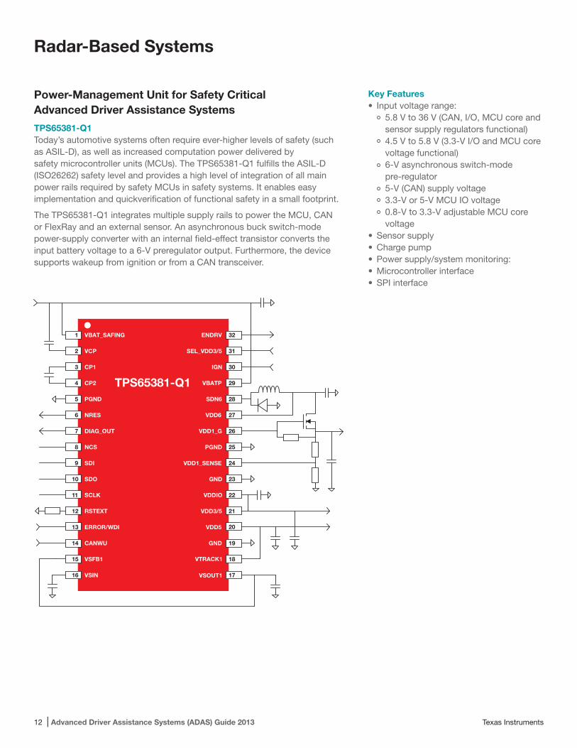
TPS65381-Q1Today’s automotive systems often require ever-higher levels of safety (suchas ASIL-D), as well as increased computation power delivered bysafety microcontroller units (MCUs). The TPS65381-Q1 fulfills the ASIL-D (ISO26262) safety level and provides a high level of integration of all main power rails required by safety MCUs in safety systems. It enables easy implementation and quickverification of functional safety in a small footprint.
The TPS65381-Q1 integrates multiple supply rails to power the MCU, CANor FlexRay and an external sensor. An asynchronous buck switch-modepower-supply converter with an internal field-effect transistor converts the input battery voltage to a 6-V preregulator output. Furthermore, the device supports wakeup from ignition or from a CAN transceiver.
Key Features• Input voltage range:
5.8 V to 36 V (CAN, I/O, MCU core and sensor supply regulators functional)4.5 V to 5.8 V (3.3-V I/O and MCU core voltage functional)6-V asynchronous switch-mode
pre-regulator 5-V (CAN) supply voltage3.3-V or 5-V MCU IO voltage0.8-V to 3.3-V adjustable MCU core voltage
• Sensor supply• Charge pump• Power supply/system monitoring:• Microcontroller interface• SPI interface
TPS65381-Q1CP2
CP1
VCP
ERROR/WDI
PGND
VBAT_SAFING
CANWU
DIAG_OUT
VSIN
VSFB1 VTRACK1
VSOUT1
VDD6
VDD3/5
VDDIO
VDD1_G
SDN6
VBATP
IGN
VDD1_SENSE
GND
VDD5
ENDRV
SEL_VDD3/5
PGND
GNDSDO
NCS
SDI
SCLK
NRES
RSTEXT
1
2
4
13
14
3
15
16
5
6
7
8
9
10
11
12
32
31
30
29
28
27
26
25
24
23
22
21
20
19
18
17
Texas Instruments Advanced Driver Assistance Systems (ADAS) Guide 2013 | 13
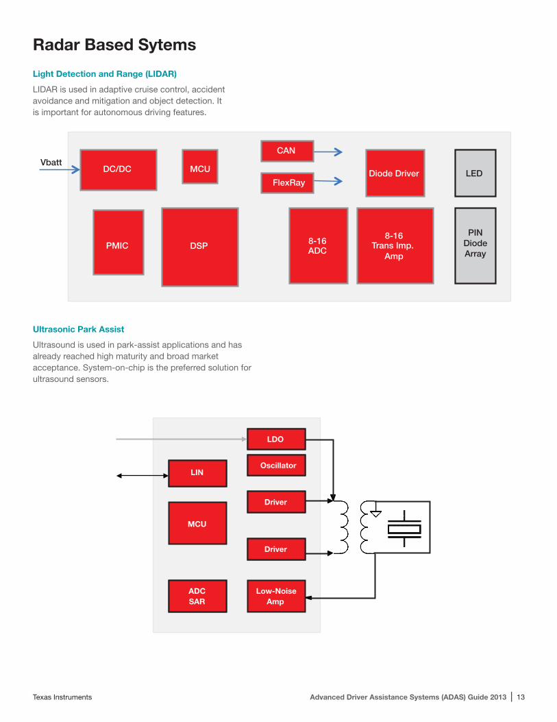
Radar Based Sytems
Light Detection and Range (LIDAR)
LIDAR is used in adaptive cruise control, accident avoidance and mitigation and object detection. It is important for autonomous driving features.
DSP PMIC
MCU
8-16 Trans Imp.
Amp 8-16 ADC
DC/DC Vbatt
PINDiode Array
Diode Driver LED
CAN
FlexRay
Ultrasonic Park Assist
Ultrasound is used in park-assist applications and has already reached high maturity and broad market acceptance. System-on-chip is the preferred solution for ultrasound sensors.
ADC SAR
MCU
LDO
Oscillator
Driver
Driver
Low-Noise Amp
LIN
14 | Advanced Driver Assistance Systems (ADAS) Guide 2013 Texas Instruments
Sensor FusionOverview
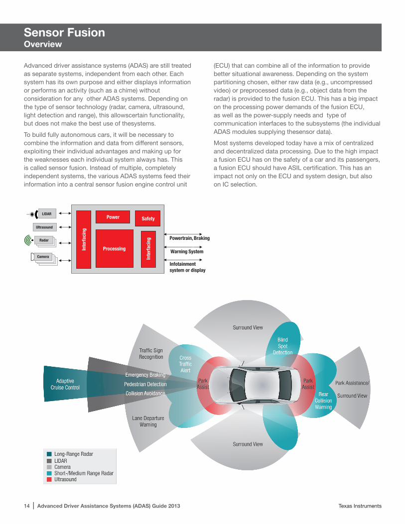
Advanced driver assistance systems (ADAS) are still treated as separate systems, independent from each other. Each system has its own purpose and either displays information or performs an activity (such as a chime) without consideration for any other ADAS systems. Depending on the type of sensor technology (radar, camera, ultrasound, light detection and range), this allowscertain functionality, but does not make the best use of thesystems.
To build fully autonomous cars, it will be necessary to combine the information and data from different sensors, exploiting their individual advantages and making up for the weaknesses each individual system always has. This is called sensor fusion. Instead of multiple, completely independent systems, the various ADAS systems feed their information into a central sensor fusion engine control unit
(ECU) that can combine all of the information to provide better situational awareness. Depending on the system partitioning chosen, either raw data (e.g., uncompressed video) or preprocessed data (e.g., object data from the radar) is provided to the fusion ECU. This has a big impact on the processing power demands of the fusion ECU, as well as the power-supply needs and type of communication interfaces to the subsystems (the individual ADAS modules supplying thesensor data).
Most systems developed today have a mix of centralized and decentralized data processing. Due to the high impact a fusion ECU has on the safety of a car and its passengers, a fusion ECU should have ASIL certification. This has an impact not only on the ECU and system design, but also on IC selection.
Infotainment system or display
Warning System
Powertrain, BrakingRadar
LIDAR
Ultrasound
Camera
Inte
rfac
ing
Inte
rfac
ing
Processing
Power Safety
Texas Instruments Advanced Driver Assistance Systems (ADAS) Guide 2013 | 15
Hercules™ Safety MCUsOverview
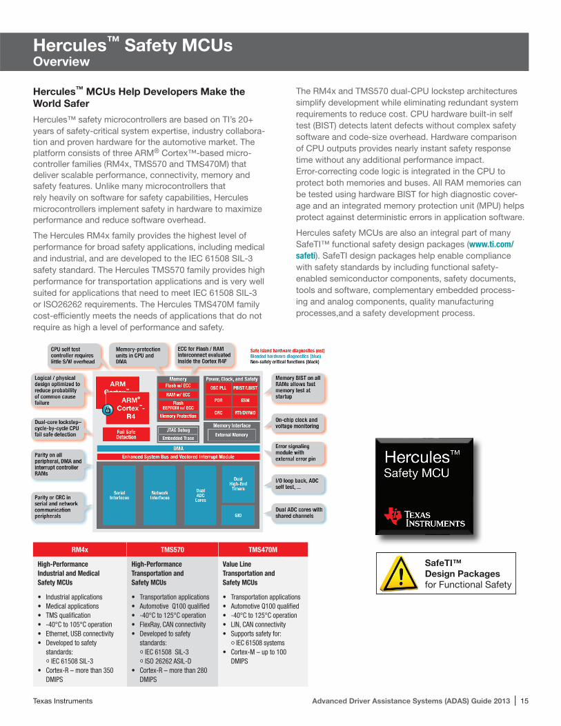
Hercules™ MCUs Help Developers Make the World Safer
Hercules™ safety microcontrollers are based on TI’s 20+ years of safety-critical system expertise, industry collabora-tion and proven hardware for the automotive market. The platform consists of three ARM® Cortex™-based micro-controller families (RM4x, TMS570 and TMS470M) that deliver scalable performance, connectivity, memory and safety features. Unlike many microcontrollers that rely heavily on software for safety capabilities, Hercules microcontrollers implement safety in hardware to maximize performance and reduce software overhead.
The Hercules RM4x family provides the highest level of perform ance for broad safety applications, including medical and industrial, and are developed to the IEC 61508 SIL-3 safety standard. The Hercules TMS570 family provides high performance for transportation applications and is very well suited for applications that need to meet IEC 61508 SIL-3 or ISO26262 requirements. The Hercules TMS470M family cost-efficiently meets the needs of applications that do not require as high a level of performance and safety.
RM4x TMS570 TMS470M
High-Performance Industrial and Medical Safety MCUs
High-Performance Transportation and Safety MCUs
Value Line Transportation and Safety MCUs
• Industrial applications• Medical applications• TMS qualification• -40°C to 105°C operation• Ethernet, USB connectivity• Developed to safety
standards: IEC 61508 SIL-3• Cortex-R – more than 350
DMIPS
• Transportation applications• Automotive Q100 qualified• -40°C to 125°C operation• FlexRay, CAN connectivity• Developed to safety
standards: IEC 61508 SIL-3 ISO 26262 ASIL-D• Cortex-R – more than 280
DMIPS
• Transportation applications• Automotive Q100 qualified• -40°C to 125°C operation• LIN, CAN connectivity• Supports safety for: IEC 61508 systems• Cortex-M – up to 100
DMIPS
SafeTI™
Design Packages
for Functional Safety
The RM4x and TMS570 dual-CPU lockstep architectures simplify development while eliminating redundant system requirements to reduce cost. CPU hardware built-in self test (BIST) detects latent defects without complex safety software and code-size overhead. Hardware comparison of CPU outputs provides nearly instant safety response time without any additional performance impact. Error-correcting code logic is integrated in the CPU to protect both memories and buses. All RAM memories can be tested using hardware BIST for high diagnostic cover-age and an integrated memory protection unit (MPU) helps protect against deterministic errors in application software.
Hercules safety MCUs are also an integral part of many SafeTI™ functional safety design packages (www.ti.com/safeti). SafeTI design packages help enable compliance with safety standards by including functional safety-enabled semiconductor components, safety documents, tools and software, complementary embedded process-ing and analog components, quality manufacturing processes,and a safety development process.
16 | Advanced Driver Assistance Systems (ADAS) Guide 2013 Texas Instruments
Hercules™ Safety MCUs
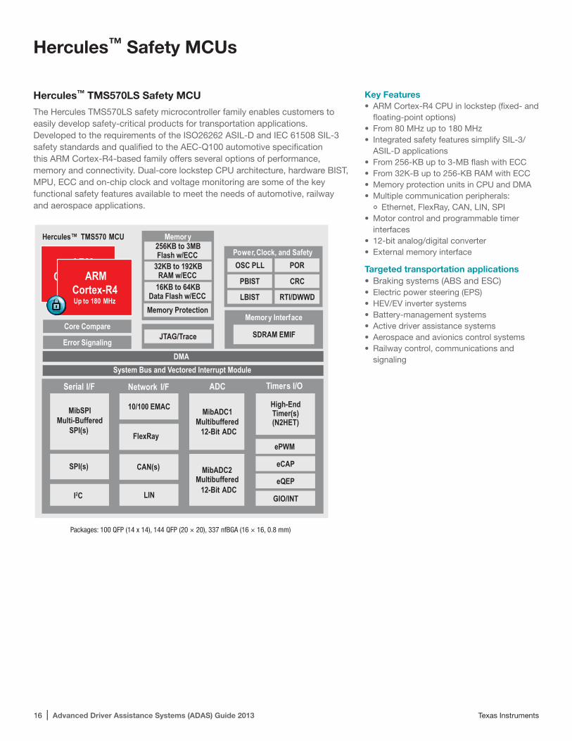
Hercules™ TMS570LS Safety MCU The Hercules TMS570LS safety microcontroller family enables customers to easily develop safety-critical products for transportation applications. Developed to the requirements of the ISO26262 ASIL-D and IEC 61508 SIL-3 safety standards and qualified to the AEC-Q100 automotive specification this ARM Cortex-R4-based family offers several options of performance, memory and connectivity. Dual-core lockstep CPU architecture, hardware BIST, MPU, ECC and on-chip clock and voltage monitoring are some of the key functional safety features available to meet the needs of automotive, railway and aerospace applications.
Key Features• ARM Cortex-R4 CPU in lockstep (fixed- and
floating-point options)• From 80 MHz up to 180 MHz• Integrated safety features simplify SIL-3/
ASIL-D applications• From 256-KB up to 3-MB flash with ECC• From 32K-B up to 256-KB RAM with ECC• Memory protection units in CPU and DMA• Multiple communication peripherals:
Ethernet, FlexRay, CAN, LIN, SPI• Motor control and programmable timer
interfaces• 12-bit analog/digital converter• External memory interface
Targeted transportation applications• Braking systems (ABS and ESC)• Electric power steering (EPS) • HEV/EV inverter systems • Battery-management systems • Active driver assistance systems • Aerospace and avionics control systems• Railway control, communications and
signaling
Packages: 100 QFP (14 x 14), 144 QFP (20 × 20), 337 nfBGA (16 × 16, 0.8 mm)
POROSC PLL
PBIST
LBIST RTI/DWWD
CRC
DMA
Memory256KB to 3MBFlash w/ECC
32KB to 192KBRAM w/ECC
Power,Clock, and Safety
Memory Interface
SDRAM EMIFJTAG/TraceCore Compare
Error Signaling
ARM ®
160MHz
™
Timers I/O
MibSPIMulti-Buffered
SPI(s)
Serial I/F Network I/F ADC
MibADC1Multibuffered
12-Bit ADC
MibADC2
12-Bit ADCLIN
High-EndTimer(s)(N2HET)
I2C
SPI(s)
FlexRay
CAN(s)
16KB to 64KBData Flash w/ECC
ePWM
GIO/INT
eCAP
eQEP
10/100 EMAC
Hercules™ TMS570 MCU
Memory Protection
ARMCortex™-R4Up to 220 MHz
ARMCortex-R4Up to 180 MHz
System Bus and Vectored Interrupt Module
Multibuffered

Texas Instruments Advanced Driver Assistance Systems (ADAS) Guide 2013 | 17
Hercules™ Evaluation and Development Kits
Low-Cost USB Stick Evaluation/Development Kits
TMDXRM48USB – RM48 USB Stick KitTMDX570LS31USB – TMS570 USB Stick KitTMDX470MF066USB – TMS470M USB Stick Kit
USB stick kit features:• USB powered• On-board USB XDS100v2 JTAG debugging• On-board SCI-to-PC serial communication• Access to select signal-pin test points• LEDs, temp sensor and light sensor• CAN transceiver• Includes Code Composer Studio™ IDE, HALCoGen and code examples $79
Eva
luat
ion $79
Hercules™ Development Kits
TMDX570LS31HDK – TMS570LS31x/21x Development KitTMDX570LS12HDK – TMS570LS12x/11x Development KitTMDX570LS04HDK – TMS570LS04x/03x Development KitTMDX470MF066HDK – TMS470M Development Kit
Hercules development kit features:• On-board USB XDS100v2 JTAG debugging• On-board SCI-to-PC serial communication• External JTAG and 32-bit ETM trace (RM48 and TMS570LS31)• Access to signal-pin test points• LEDs, temp sensor and light sensor• Two CAN transceivers• RJ-45 10/100 Ethernet interface (RM48/RM46 and TMS570LS31/12)• USB-A host and USB-B device interfaces (RM48)• Includes Code Composer Studio™ IDE, HALCoGen, and code examples $199
Dev
elo
pm
ent
$199
TMDXRM48HDK – RM48 Development KitTMDXRM46HDK – RM46 Development KitTMDXRM42HDK – RM42 Development Kit
Hercules™ Safety MCUs
18 | Advanced Driver Assistance Systems (ADAS) Guide 2013 Texas Instruments
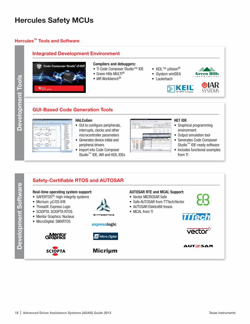
Hercules™ Tools and Software
Integrated Development Environment
Dev
elo
pm
ent
Too
ls
GUI-Based Code Generation Tools
HALCoGen• GUI to configure peripherals,
interrupts, clocks and other microcontroller parameters• Generates device initial and
peripheral drivers • Import into Code Composer
Studio™ IDE, IAR and KEIL IDEs
HET IDE• Graphical programming
environment• Output simulation tool• Generates Code Composer
Studio™ IDE-ready software• Includes functional examples
from TI
Dev
elo
pm
ent
So
ftw
are
Safety-Certifiable RTOS and AUTOSAR
Real-time operating system support:• SAFERTOS®: high-integrity systems• Micrium: μC/OS II/III• ThreadX: Express Logic• SCIOPTA: SCIOPTA RTOS• Mentor Graphics: Nucleus• MicroDigital: SMXRTOS
AUTOSAR RTE and MCAL Support:• Vector MICROSAR Safe• Safe AUTOSAR from TTTech/Vector• AUTOSAR ElektroBit tresos• MCAL from TI
Hercules Safety MCUs
• KEIL™ µVision®
• iSystem winIDEA• Lauterbach
Compilers and debuggers:• TI Code Composer Studio™ IDE• Green Hills MULTI®
• IAR Workbench®
Texas Instruments Advanced Driver Assistance Systems (ADAS) Guide 2013 | 19
Selection Tables
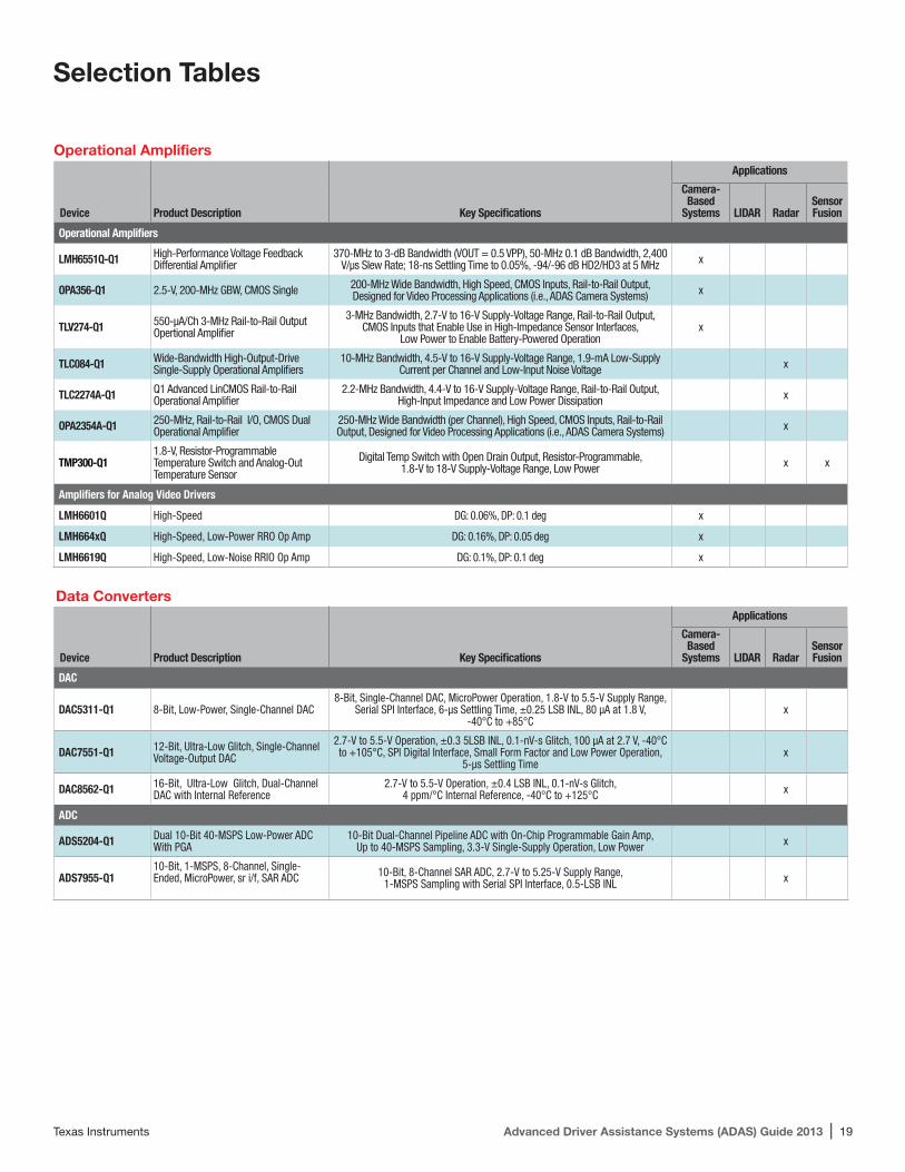
Operational Amplifiers
Device Product Description Key Specifications
Applications
Camera-Based
Systems LIDAR RadarSensorFusion
Operational Amplifiers
LMH6551Q-Q1 High-Performance Voltage Feedback Differential Amplifier
370-MHz to 3-dB Bandwidth (VOUT = 0.5 VPP), 50-MHz 0.1 dB Bandwidth, 2,400 V/µs Slew Rate; 18-ns Settling Time to 0.05%, -94/-96 dB HD2/HD3 at 5 MHz x
OPA356-Q1 2.5-V, 200-MHz GBW, CMOS Single 200-MHz Wide Bandwidth, High Speed, CMOS Inputs, Rail-to-Rail Output,Designed for Video Processing Applications (i.e., ADAS Camera Systems) x
TLV274-Q1 550-µA/Ch 3-MHz Rail-to-Rail Output Opertional Amplifier
3-MHz Bandwidth, 2.7-V to 16-V Supply-Voltage Range, Rail-to-Rail Output,CMOS Inputs that Enable Use in High-Impedance Sensor Interfaces,
Low Power to Enable Battery-Powered Operationx
TLC084-Q1 Wide-Bandwidth High-Output-Drive Single-Supply Operational Amplifiers
10-MHz Bandwidth, 4.5-V to 16-V Supply-Voltage Range, 1.9-mA Low-SupplyCurrent per Channel and Low-Input Noise Voltage x
TLC2274A-Q1 Q1 Advanced LinCMOS Rail-to-RailOperational Amplifier
2.2-MHz Bandwidth, 4.4-V to 16-V Supply-Voltage Range, Rail-to-Rail Output,High-Input Impedance and Low Power Dissipation x
OPA2354A-Q1 250-MHz, Rail-to-Rail I/O, CMOS Dual Operational Amplifier
250-MHz Wide Bandwidth (per Channel), High Speed, CMOS Inputs, Rail-to-Rail Output, Designed for Video Processing Applications (i.e., ADAS Camera Systems) x
TMP300-Q11.8-V, Resistor-Programmable Temperature Switch and Analog-Out Temperature Sensor
Digital Temp Switch with Open Drain Output, Resistor-Programmable, 1.8-V to 18-V Supply-Voltage Range, Low Power x x
Amplifiers for Analog Video Drivers
LMH6601Q High-Speed DG: 0.06%, DP: 0.1 deg x
LMH664xQ High-Speed, Low-Power RRO Op Amp DG: 0.16%, DP: 0.05 deg x
LMH6619Q High-Speed, Low-Noise RRIO Op Amp DG: 0.1%, DP: 0.1 deg x
Data Converters
Device Product Description Key Specifications
Applications
Camera-Based
Systems LIDAR RadarSensorFusion
DAC
DAC5311-Q1 8-Bit, Low-Power, Single-Channel DAC8-Bit, Single-Channel DAC, MicroPower Operation, 1.8-V to 5.5-V Supply Range,
Serial SPI Interface, 6-μs Settling Time, ±0.25 LSB INL, 80 μA at 1.8 V,-40°C to +85°C
x
DAC7551-Q1 12-Bit, Ultra-Low Glitch, Single-ChannelVoltage-Output DAC
2.7-V to 5.5-V Operation, ±0.3 5LSB INL, 0.1-nV-s Glitch, 100 μA at 2.7 V, -40°C to +105°C, SPI Digital Interface, Small Form Factor and Low Power Operation,
5-μs Settling Timex
DAC8562-Q1 16-Bit, Ultra-Low Glitch, Dual-Channel DAC with Internal Reference
2.7-V to 5.5-V Operation, ±0.4 LSB INL, 0.1-nV-s Glitch,4 ppm/°C Internal Reference, -40°C to +125°C x
ADC
ADS5204-Q1 Dual 10-Bit 40-MSPS Low-Power ADC With PGA
10-Bit Dual-Channel Pipeline ADC with On-Chip Programmable Gain Amp,Up to 40-MSPS Sampling, 3.3-V Single-Supply Operation, Low Power x
ADS7955-Q110-Bit, 1-MSPS, 8-Channel, Single-Ended, MicroPower, sr i/f, SAR ADC 10-Bit, 8-Channel SAR ADC, 2.7-V to 5.25-V Supply Range,
1-MSPS Sampling with Serial SPI Interface, 0.5-LSB INL x
20 | Advanced Driver Assistance Systems (ADAS) Guide 2013 Texas Instruments
Selection Tables
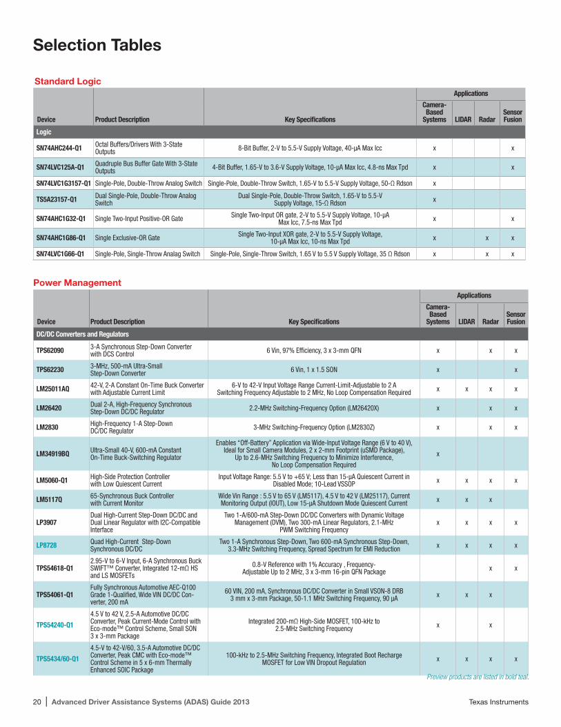
Power Management
Device Product Description Key Specifications
Applications
Camera-Based
Systems LIDAR RadarSensorFusion
DC/DC Converters and Regulators
TPS62090 3-A Synchronous Step-Down Converterwith DCS Control 6 Vin, 97% Efficiency, 3 x 3-mm QFN x x x
TPS62230 3-MHz, 500-mA Ultra-SmallStep-Down Converter 6 Vin, 1 x 1.5 SON x x
LM25011AQ 42-V, 2-A Constant On-Time Buck Converterwith Adjustable Current Limit
6-V to 42-V Input Voltage Range Current-Limit-Adjustable to 2 ASwitching Frequency Adjustable to 2 MHz, No Loop Compensation Required x x x x
LM26420 Dual 2-A, High-Frequency SynchronousStep-Down DC/DC Regulator 2.2-MHz Switching-Frequency Option (LM26420X) x x x
LM2830 High-Frequency 1-A Step-DownDC/DC Regulator 3-MHz Switching-Frequency Option (LM2830Z) x x x
LM34919BQ Ultra-Small 40-V, 600-mA ConstantOn-Time Buck-Switching Regulator
Enables “Off-Battery” Application via Wide-Input Voltage Range (6 V to 40 V),Ideal for Small Camera Modules, 2 x 2-mm Footprint (uSMD Package),
Up to 2.6-MHz Switching Frequency to Minimize Interference, No Loop Compensation Required
x
LM5060-Q1 High-Side Protection Controller with Low Quiescent Current
Input Voltage Range: 5.5 V to +65 V; Less than 15-μA Quiescent Current in Disabled Mode; 10-Lead VSSOP x x x x
LM5117Q 65-Synchronous Buck Controller with Current Monitor
Wide Vin Range : 5.5 V to 65 V (LM5117), 4.5 V to 42 V (LM25117), CurrentMonitoring Output (IOUT), Low 15-µA Shutdown Mode Quiescent Current x x x
LP3907Dual High-Current Step-Down DC/DC andDual Linear Regulator with I2C-CompatibleInterface
Two 1-A/600-mA Step-Down DC/DC Converters with Dynamic Voltage Management (DVM), Two 300-mA Linear Regulators, 2.1-MHz
PWM Switching Frequencyx x x x
LP8728 Quad High-Current Step-Down Synchronous DC/DC
Two 1-A Synchronous Step-Down, Two 600-mA Synchronous Step-Down, 3.3-MHz Switching Frequency, Spread Spectrum for EMI Reduction x x x x
TPS54618-Q12.95-V to 6-V Input, 6-A Synchronous BuckSWIFT™ Converter, Integrated 12-mΩ HSand LS MOSFETs
0.8-V Reference with 1% Accuracy , Frequency-Adjustable Up to 2 MHz, 3 x 3-mm 16-pin QFN Package x x
TPS54061-Q1Fully Synchronous Automotive AEC-Q100 Grade 1-Qualified, Wide VIN DC/DC Con-verter, 200 mA
60 VIN, 200 mA, Synchronous DC/DC Converter in Small VSON-8 DRB3 mm x 3-mm Package, 50-1.1 MHz Switching Frequency, 90 µA x x x
TPS54240-Q1
4.5 V to 42 V, 2.5-A Automotive DC/DCConverter, Peak Current-Mode Control withEco-mode™ Control Scheme, Small SON 3 x 3-mm Package
Integrated 200-mΩ High-Side MOSFET, 100-kHz to2.5-MHz Switching Frequency x x
TPS5434/60-Q1
4.5-V to 42-V/60, 3.5-A Automotive DC/DCConverter, Peak CMC with Eco-mode™ Control Scheme in 5 x 6-mm Thermally Enhanced SOIC Package
100-kHz to 2.5-MHz Switching Frequency, Integrated Boot RechargeMOSFET for Low VIN Dropout Regulation x x x x
Standard Logic
Device Product Description Key Specifications
Applications
Camera-Based
Systems LIDAR RadarSensorFusion
Logic
SN74AHC244-Q1 Octal Buffers/Drivers With 3-State Outputs 8-Bit Buffer, 2-V to 5.5-V Supply Voltage, 40-µA Max Icc x x
SN74LVC125A-Q1 Quadruple Bus Buffer Gate With 3-State Outputs 4-Bit Buffer, 1.65-V to 3.6-V Supply Voltage, 10-µA Max Icc, 4.8-ns Max Tpd x x
SN74LVC1G3157-Q1 Single-Pole, Double-Throw Analog Switch Single-Pole, Double-Throw Switch, 1.65-V to 5.5-V Supply Voltage, 50-Ω Rdson x
TS5A23157-Q1 Dual Single-Pole, Double-Throw Analog Switch
Dual Single-Pole, Double-Throw Switch, 1.65-V to 5.5-VSupply Voltage, 15-Ω Rdson x
SN74AHC1G32-Q1 Single Two-Input Positive-OR Gate Single Two-Input OR gate, 2-V to 5.5-V Supply Voltage, 10-µAMax Icc, 7.5-ns Max Tpd x x
SN74AHC1G86-Q1 Single Exclusive-OR Gate Single Two-Input XOR gate, 2-V to 5.5-V Supply Voltage,10-µA Max Icc, 10-ns Max Tpd x x x
SN74LVC1G66-Q1 Single-Pole, Single-Throw Analag Switch Single-Pole, Single-Throw Switch, 1.65 V to 5.5 V Supply Voltage, 35 Ω Rdson x x x
Preview products are listed in bold teal.
Texas Instruments Advanced Driver Assistance Systems (ADAS) Guide 2013 | 21
Selection Tables
TPS65311-Q1 High-Voltage Power-Management IC for Automotive Safety Applications
Single 490-kHz DC/DC Controller, Dual 2.45-MHz DC/DC Buck Converter, Single Adjustable 350-mA Linear Regulator x x
TPS65300-Q1 Automotive 3-MHz Step-Down Regulator, Triple Linear Regulators
3-MHz Step-Down Regulator, Single Linear Regulator and Dual Linear Regulator Controllers x
TPS65381-Q1 Multirail Power Supply for Microcontrollers in Safety-Critical Applications
Wide-Input Voltage Buck Converter, LDOs Including Sensor Supply, Question-and-Answer Watchdog, Enhanced Diagnostics and BIST x x
TPS659119-Q1 Multirail Power Supply with Three DC/DC Converters and Eight LDOs
Three DC/DC Converters, Control Signal for External DC/DC Converter, Eight LDOs, I2C Interface, Watchdog Timer x x
TPS43331-Q1 Automotive Catalog Dual Switcher and Linear Regulators Multirail Power Supply
Wide-Voltage Supply Range from 5 V to 30 V (up to 40-V Transient), Dual Adjustable Output Voltage, Step-Down Controllers and Dual Programmable LDOs x
LDOs
TPS78225-Q1TPS78227-Q1TPS78228-Q1TPS78230-Q1
150-mA, Ultra-Low Quiescent Current,1-μA IqLow-Dropout Linear Regulator with EN Function, Fixed Voltage Options: 2.5 V 2.7 V, 2.8 V, 3 V
Low Iq, 1 µA when IOUT=0 mA, 8 µA when IOUT=15 0mA, Low-Dropout Voltage: 130 mV at 150 mA, VIN 2.2 V to 5.5 V, Stable with
1-µF Ceramic Capacitors, Thermal Shutdown and Overcurrent Protectionsx x x x
TPS76201-Q1Low-Output, Adjustable, Ultra-Low-Power, 100-mA Low-Dropout Linear Regulator with EN Function
Adjustable Output Voltage: 0.7 V to 5.5 V, Input Voltage2.7 V to 10 V, 27-μA Quiescent Current at 100 mA,
1 µA in Standby Mode, Overcurrent Protectionx x x x
TPS75201-Q1 Fast Transient Response 2-A Low DropoutVoltage Regulator with Reset
Adjustable Output Voltage 1.5 V to 5 V, Input Voltage 2.7 V to5.5 V, Typically 210-mV Dropout Voltage at 2 A, Ultra-Low75-μA Quiescent Current, Thermal Shutdown Protection
x x x x
TPS74801-Q1 1.5-A Low-Dropout Linear Regulator withProgrammable Soft Start
VOUT Range 0.8 V to 3.6 V, 5.5-V Max Input Voltage, 60-mV Low-Dropout Voltageat 1.5 A, Programmable Soft Start, Stable with Any
Output Cap > = 2.2 µF, Good Transient Response Under Low VINx x x x
TPS74701-Q1 500-mA Low-Dropout Linear Regulator withProgrammable Soft Start
VOUT Range 0.8 V to 3.6 V, 5.5-V Max Input Voltage, 50-mV Low-Dropout Voltageat 500 mA, Programmable Soft Start, Stable with Any
Output Cap > = 2.2 µF, Good Transient Response Under Low VINx x x x
TPS73601-Q1 Cap-Free, NMOS, 400-mA Low-DropoutRegulator with Reverse Current Protection
VIN Range from 1.7 V to 5.5 V, Stable with No Output Cap, 75-mV Ultra-Low Dropout Voltage, Excellent Load Transient, Low Noise: 30 μVRMS (10 KHz to
100 KHz), Adjustable Output Voltage: 1.2 V to 5.5 V, Thermal Shutdown Protectionx x x x
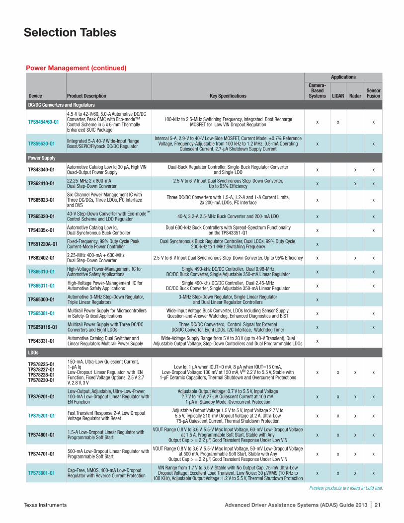
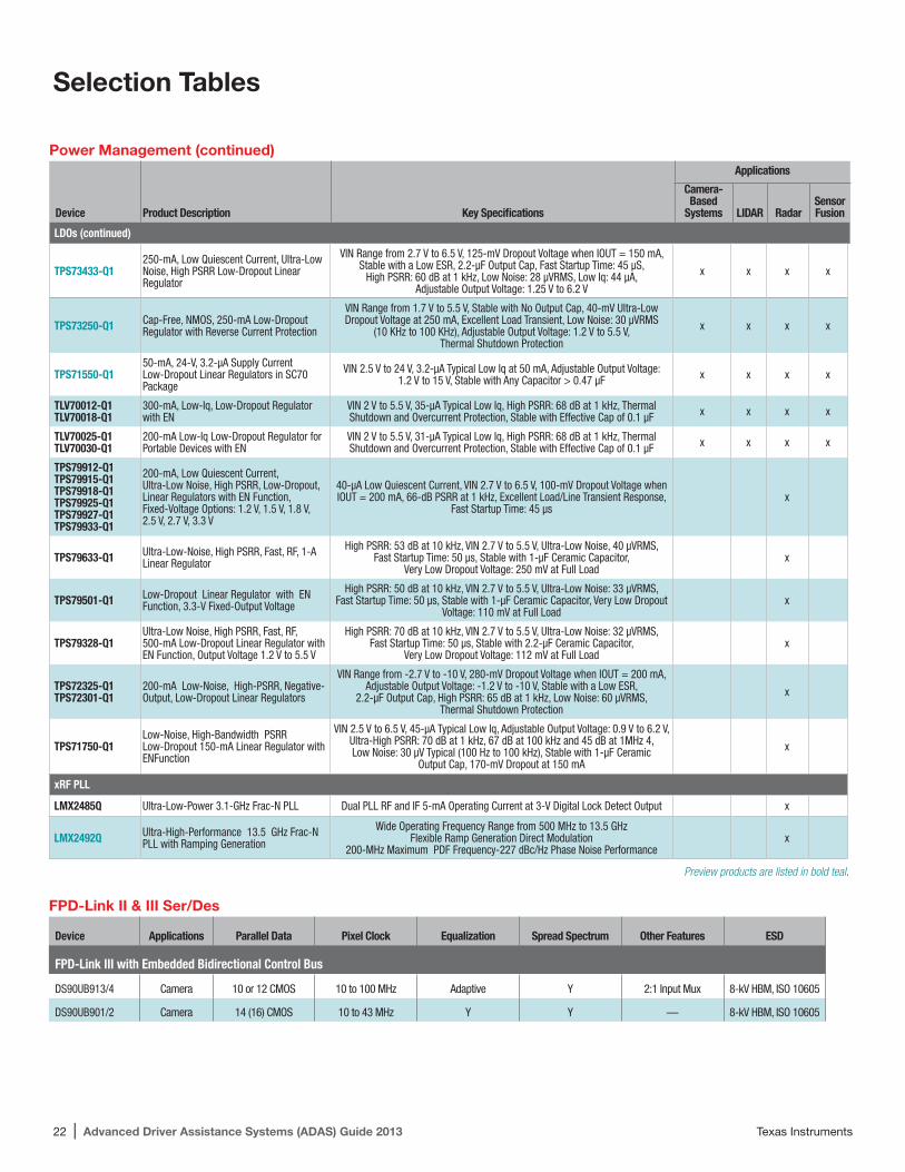
Power Management (continued)
Device Product Description Key Specifications
Applications
Camera-Based
Systems LIDAR RadarSensorFusion
DC/DC Converters and Regulators
TPS5454/60-Q1
4.5-V to 42-V/60, 5.0-A Automotive DC/DCConverter, Peak CMC with Eco-mode™ Control Scheme in 5 x 6-mm Thermally Enhanced SOIC Package
100-kHz to 2.5-MHz Switching Frequency, Integrated Boot Recharge MOSFET for Low VIN Dropout Regulation x x x
TPS55530-Q1 IIntegrated 5-A 40-V Wide-Input RangeBoost/SEPIC/Flyback DC/DC Regulator
Internal 5-A, 2.9-V to 40-V Low-Side MOSFET, Current Mode, ±0.7% ReferenceVoltage, Frequency-Adjustable from 100 kHz to 1.2 MHz, 0.5-mA Operating
Quiescent Current, 2.7-μA Shutdown Supply Currentx x
Power Supply
TPS43340-Q1 Automotive Catalog Low Iq 30 µA, High VINQuad-Output Power Supply
Dual-Buck Regulator Controller, Single-Buck Regulator Converterand Single LDO x x x
TPS62410-Q1 22.25-MHz 2 x 800-mADual Step-Down Converter
2.5-V to 6-V Input Dual Synchronous Step-Down Converter,Up to 95% Efficiency x x x
TPS65023-Q1Six-Channel Power Management IC with Three DC/DCs, Three LDOs, I2C Interface and DVS
Three DC/DC Converters with 1.5-A, 1.2-A and 1-A Current Limits, 2x 200-mA LDOs, I2C Interface x x
TPS65320-Q1 40-V Step-Down Converter with Eco-mode™ Control Scheme and LDO Regulator 40-V, 3.2-A 2.5-MHz Buck Converter and 200-mA LDO x x
TPS4335x-Q1 Automotive Catalog Low Iq, Dual Synchronous Buck Controller
Dual 600-kHz Buck Controllers with Spread-Spectrum Functionality on the TPS43351-Q1 x x
TPS51220A-Q1 Fixed-Frequency, 99% Duty Cycle PeakCurrent-Mode Power Controller
Dual Synchronous Buck Regulator Controller, Dual LDOs, 99% Duty Cycle,200-kHz to 1-MHz Switching Frequency x
TPS62402-Q1 2.25-MHz 400-mA + 600-MHzDual Step-Down Converter 2.5-V to 6-V Input Dual Synchronous Step-Down Converter, Up to 95% Efficiency x x x
TPS65310-Q1 High-Voltage Power-Management IC for Automotive Safety Applications
Single 490-kHz DC/DC Controller, Dual 0.98-MHz DC/DC Buck Converter, Single Adjustable 350-mA Linear Regulator x x
Preview products are listed in bold teal.
22 | Advanced Driver Assistance Systems (ADAS) Guide 2013 Texas Instruments
Power Management (continued)
Device Product Description Key Specifications
Applications
Camera-Based
Systems LIDAR RadarSensorFusion
LDOs (continued)
Selection Tables
TPS73433-Q1250-mA, Low Quiescent Current, Ultra-Low Noise, High PSRR Low-Dropout Linear Regulator
VIN Range from 2.7 V to 6.5 V, 125-mV Dropout Voltage when IOUT = 150 mA,Stable with a Low ESR, 2.2-µF Output Cap, Fast Startup Time: 45 μS,
High PSRR: 60 dB at 1 kHz, Low Noise: 28 μVRMS, Low Iq: 44 μA,Adjustable Output Voltage: 1.25 V to 6.2 V
x x x x
TPS73250-Q1 Cap-Free, NMOS, 250-mA Low-Dropout Regulator with Reverse Current Protection
VIN Range from 1.7 V to 5.5 V, Stable with No Output Cap, 40-mV Ultra-Low Dropout Voltage at 250 mA, Excellent Load Transient, Low Noise: 30 μVRMS
(10 KHz to 100 KHz), Adjustable Output Voltage: 1.2 V to 5.5 V, Thermal Shutdown Protection
x x x x
TPS71550-Q150-mA, 24-V, 3.2-μA Supply CurrentLow-Dropout Linear Regulators in SC70 Package
VIN 2.5 V to 24 V, 3.2-μA Typical Low Iq at 50 mA, Adjustable Output Voltage:1.2 V to 15 V, Stable with Any Capacitor > 0.47 μF x x x x
TLV70012-Q1TLV70018-Q1
300-mA, Low-Iq, Low-Dropout Regulator with EN
VIN 2 V to 5.5 V, 35-μA Typical Low Iq, High PSRR: 68 dB at 1 kHz, ThermalShutdown and Overcurrent Protection, Stable with Effective Cap of 0.1 μF x x x x
TLV70025-Q1TLV70030-Q1
200-mA Low-Iq Low-Dropout Regulator for Portable Devices with EN
VIN 2 V to 5.5 V, 31-μA Typical Low Iq, High PSRR: 68 dB at 1 kHz, ThermalShutdown and Overcurrent Protection, Stable with Effective Cap of 0.1 μF x x x x
TPS79912-Q1TPS79915-Q1TPS79918-Q1TPS79925-Q1TPS79927-Q1TPS79933-Q1
200-mA, Low Quiescent Current,Ultra-Low Noise, High PSRR, Low-Dropout, Linear Regulators with EN Function, Fixed-Voltage Options: 1.2 V, 1.5 V, 1.8 V,2.5 V, 2.7 V, 3.3 V
40-μA Low Quiescent Current, VIN 2.7 V to 6.5 V, 100-mV Dropout Voltage whenIOUT = 200 mA, 66-dB PSRR at 1 kHz, Excellent Load/Line Transient Response,
Fast Startup Time: 45 μsx
TPS79633-Q1 Ultra-Low-Noise, High PSRR, Fast, RF, 1-A Linear Regulator
High PSRR: 53 dB at 10 kHz, VIN 2.7 V to 5.5 V, Ultra-Low Noise, 40 μVRMS,Fast Startup Time: 50 μs, Stable with 1-μF Ceramic Capacitor,
Very Low Dropout Voltage: 250 mV at Full Loadx
TPS79501-Q1 Low-Dropout Linear Regulator with EN Function, 3.3-V Fixed-Output Voltage
High PSRR: 50 dB at 10 kHz, VIN 2.7 V to 5.5 V, Ultra-Low Noise: 33 μVRMS,Fast Startup Time: 50 μs, Stable with 1-μF Ceramic Capacitor, Very Low Dropout
Voltage: 110 mV at Full Loadx
TPS79328-Q1Ultra-Low Noise, High PSRR, Fast, RF, 500-mA Low-Dropout Linear Regulator withEN Function, Output Voltage 1.2 V to 5.5 V
High PSRR: 70 dB at 10 kHz, VIN 2.7 V to 5.5 V, Ultra-Low Noise: 32 μVRMS,Fast Startup Time: 50 μs, Stable with 2.2-μF Ceramic Capacitor,
Very Low Dropout Voltage: 112 mV at Full Loadx
TPS72325-Q1TPS72301-Q1
200-mA Low-Noise, High-PSRR, Negative-Output, Low-Dropout Linear Regulators
VIN Range from -2.7 V to -10 V, 280-mV Dropout Voltage when IOUT = 200 mA,Adjustable Output Voltage: -1.2 V to -10 V, Stable with a Low ESR,
2.2-μF Output Cap, High PSRR: 65 dB at 1 kHz, Low Noise: 60 μVRMS, Thermal Shutdown Protection
x
TPS71750-Q1Low-Noise, High-Bandwidth PSRRLow-Dropout 150-mA Linear Regulator with ENFunction
VIN 2.5 V to 6.5 V, 45-µA Typical Low Iq, Adjustable Output Voltage: 0.9 V to 6.2 V,Ultra-High PSRR: 70 dB at 1 kHz, 67 dB at 100 kHz and 45 dB at 1MHz 4,Low Noise: 30 μV Typical (100 Hz to 100 kHz), Stable with 1-µF Ceramic
Output Cap, 170-mV Dropout at 150 mA
x
xRF PLL
LMX2485Q Ultra-Low-Power 3.1-GHz Frac-N PLL Dual PLL RF and IF 5-mA Operating Current at 3-V Digital Lock Detect Output x
LMX2492Q Ultra-High-Performance 13.5 GHz Frac-N PLL with Ramping Generation
Wide Operating Frequency Range from 500 MHz to 13.5 GHzFlexible Ramp Generation Direct Modulation
200-MHz Maximum PDF Frequency-227 dBc/Hz Phase Noise Performancex
Preview products are listed in bold teal.
FPD-Link II & III Ser/Des
Device Applications Parallel Data Pixel Clock Equalization Spread Spectrum Other Features ESD
FPD-Link III with Embedded Bidirectional Control Bus
DS90UB913/4 Camera 10 or 12 CMOS 10 to 100 MHz Adaptive Y 2:1 Input Mux 8-kV HBM, ISO 10605
DS90UB901/2 Camera 14 (16) CMOS 10 to 43 MHz Y Y — 8-kV HBM, ISO 10605
Texas Instruments Advanced Driver Assistance Systems (ADAS) Guide 2013 | 23
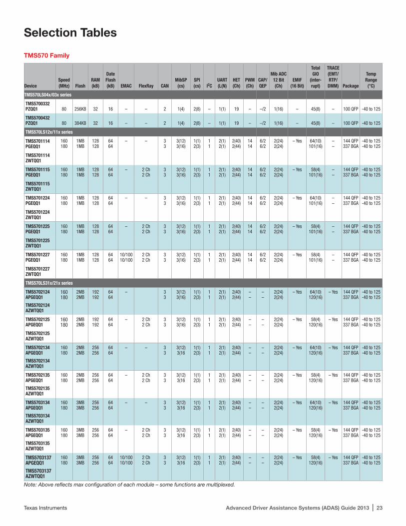
TMS570 Family
DeviceSpeed(MHz) Flash
RAM(kB)
DateFlash(kB) EMAC FlexRay CAN
MibSP(cs)
SPI(cs) I2C
UART(L(N)
HET(Ch)
PWM(Ch)
CAP/QEP
Mib ADC 12 Bit (Ch)
EMIF(16 Bit)
TotalGIO
(inter-rupt)
TRACE(EMT/RTP/DMM) Package
TempRange
(°C)
TMS570LS04x/03x series
TMS5700332PZQQ1 80 256KB 32 16 – – 2 1(4) 2(8) – 1(1) 19 – –/2 1(16) – 45(8) – 100 QFP -40 to 125
TMS5700432PZQQ1 80 384KB 32 16 – – 2 1(4) 2(8) – 1(1) 19 – –/2 1(16) – 45(8) – 100 QFP -40 to 125
TMS570LS12x/11x series
TMS5701114PGEQQ1
160180
1MB1MB
128128
6464
– – 33
3(12)3(16)
1(1)2(3)
11
2(1)2(1)
2(40)2(44)
1414
6/26/2
2(24)2(24)
– Yes 64(10)101(16)
––
144 QFP337 BGA
-40 to 125-40 to 125
TMS5701114ZWTQQ1
TMS5701115PGEQQ1
160180
1MB1MB
128128
6464
– 2 Ch2 Ch
33
3(12)3(16)
1(1)2(3)
11
2(1)2(1)
2(40)2(44)
1414
6/26/2
2(24)2(24)
– Yes 58(4)101(16)
––
144 QFP337 BGA
-40 to 125-40 to 125
TMS5701115ZWTQQ1
TMS5701224PGEQQ1
160180
1MB1MB
128128
6464
– – 33
3(12)3(16)
1(1)2(3)
11
2(1)2(1)
2(40)2(44)
1414
6/26/2
2(24)2(24)
– Yes 64(10)101(16)
––
144 QFP337 BGA
-40 to 125-40 to 125
TMS5701224ZWTQQ1
TMS5701225PGEQQ1
160180
1MB1MB
128128
6464
– 2 Ch2 Ch
33
3(12)3(16)
1(1)2(3)
11
2(1)2(1)
2(40)2(44)
1414
6/26/2
2(24)2(24)
– Yes 58(4)101(16)
––
144 QFP337 BGA
-40 to 125-40 to 125
TMS5701225ZWTQQ1
TMS5701227PGEQQ1
160180
1MB1MB
128128
6464
10/10010/100
2 Ch2 Ch
33
3(12)3(16)
1(1)2(3)
11
2(1)2(1)
2(40)2(44)
1414
6/26/2
2(24)2(24)
– Yes 58(4)101(16)
––
144 QFP337 BGA
-40 to 125-40 to 125
TMS5701227ZWTQQ1
TMS570LS31x/21x series
TMS5702124APGEQQ1
TMS5702124AZWTQQ1
160180
2MB2MB
192192
6464
– 33
3(12)3(16)
1(1)2(3)
11
2(1)2(1)
2(40)2(44)
––
––
2(24)2(24)
– Yes 64(10)120(16)
– Yes 144 QFP337 BGA
-40 to 125-40 to 125
TMS5702125APGEQQ1
TMS5702125AZWTQQ1
160180
2MB2MB
192192
6464
– 2 Ch2 Ch
33
3(12)3(16)
1(1)2(3)
11
2(1)2(1)
2(40)2(44)
––
––
2(24)2(24)
– Yes 58(4)120(16)
– Yes 144 QFP337 BGA
-40 to 125-40 to 125
TMS5702134APGEQQ1
TMS5702134AZWTQQ1
160180
2MB2MB
256256
6464
– – 33
3(12)3(16
1(1)2(3)
11
2(1)2(1)
2(40)2(44)
––
––
2(24)2(24)
– Yes 64(10)120(16)
– Yes 144 QFP337 BGA
-40 to 125-40 to 125
TMS5702135APGEQQ1
TMS5702135AZWTQQ1
160180
2MB2MB
256256
6464
– 2 Ch2 Ch
33
3(12)3(16
1(1)2(3)
11
2(1)2(1)
2(40)2(44)
––
––
2(24)2(24)
– Yes 58(4)120(16)
– Yes 144 QFP337 BGA
-40 to 125-40 to 125
TMS5703134APGEQQ1
TMS5703134AZWTQQ1
160180
3MB3MB
256256
6464
– – 33
3(12)3(16
1(1)2(3)
11
2(1)2(1)
2(40)2(44)
––
––
2(24)2(24)
– Yes 64(10)120(16)
– Yes 144 QFP337 BGA
-40 to 125-40 to 125
TMS5703135APGEQQ1
TMS5703135AZWTQQ1
160180
3MB3MB
256256
6464
– 2 Ch2 Ch
33
3(12)3(16
1(1)2(3)
11
2(1)2(1)
2(40)2(44)
––
––
2(24)2(24)
– Yes 58(4)120(16)
– Yes 144 QFP337 BGA
-40 to 125-40 to 125
TMS5703137APGEQQ1
TMS5703137AZWTQQ1
160180
3MB3MB
256256
6464
10/10010/100
2 Ch2 Ch
33
3(12)3(16
1(1)2(3)
11
2(1)2(1)
2(40)2(44)
––
––
2(24)2(24)
– Yes 58(4)120(16)
– Yes 144 QFP337 BGA
-40 to 125-40 to 125
Note: Above reflects max configuration of each module – some functions are multiplexed.
Selection Tables
24 | Advanced Driver Assistance Systems (ADAS) Guide 2013 Texas Instruments
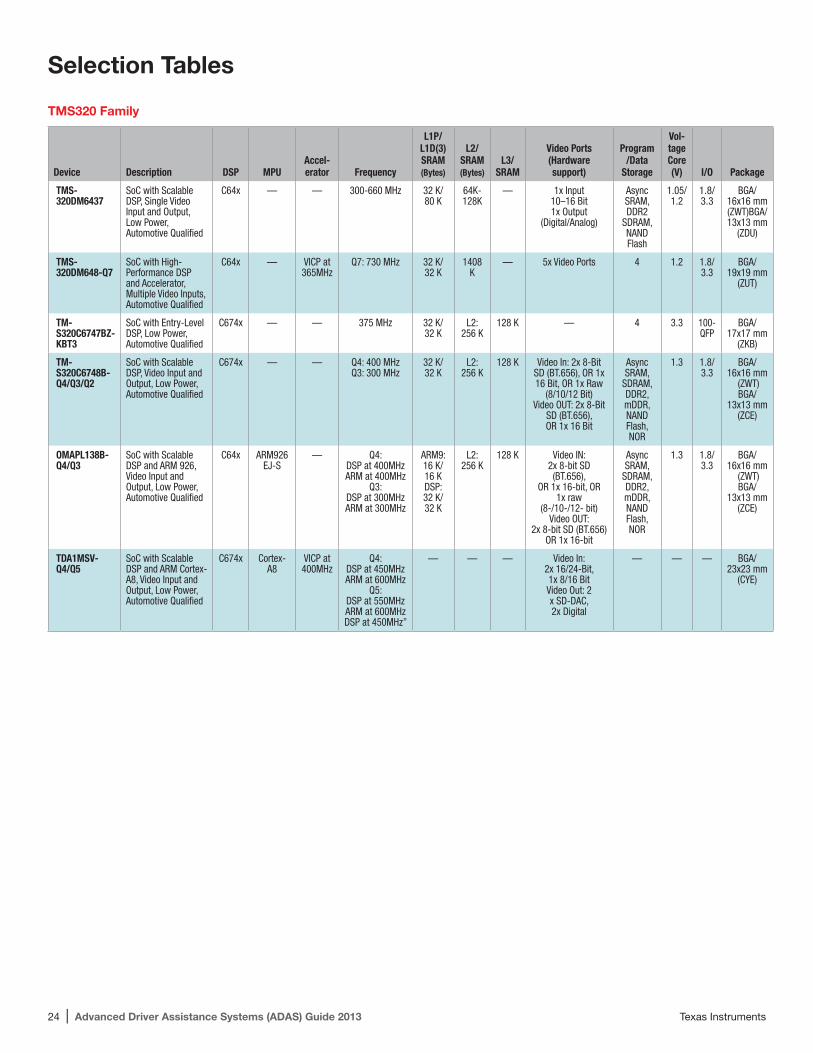
TMS320 Family
Device Description DSP MPUAccel-erator Frequency
L1P/L1D(3)SRAM(Bytes)
L2/SRAM(Bytes)
L3/SRAM
Video Ports (Hardwaresupport)
Program/Data
Storage
Vol-tageCore (V) I/O Package
TMS-320DM6437
SoC with ScalableDSP, Single VideoInput and Output,Low Power, Automotive Qualified
C64x — — 300-660 MHz 32 K/80 K
64K-128K
— 1x Input 10–16 Bit1x Output
(Digital/Analog)
Async SRAM, DDR2
SDRAM, NAND Flash
1.05/1.2
1.8/3.3
BGA/16x16 mm (ZWT)BGA/13x13 mm
(ZDU)
TMS-320DM648-Q7
SoC with High-Performance DSP and Accelerator, Multiple Video Inputs, Automotive Qualified
C64x — VICP at365MHz
Q7: 730 MHz 32 K/32 K
1408 K
— 5x Video Ports 4 1.2 1.8/3.3
BGA/19x19 mm
(ZUT)
TM- S320C6747BZ- KBT3
SoC with Entry-Level DSP, Low Power, Automotive Qualified
C674x — — 375 MHz 32 K/32 K
L2: 256 K
128 K — 4 3.3 100-QFP
BGA/17x17 mm
(ZKB)
TM- S320C6748B- Q4/Q3/Q2
SoC with Scalable DSP, Video Input and Output, Low Power, Automotive Qualified
C674x — — Q4: 400 MHzQ3: 300 MHz
32 K/32 K
L2: 256 K
128 K Video In: 2x 8-Bit SD (BT.656), OR 1x 16 Bit, OR 1x Raw
(8/10/12 Bit)Video OUT: 2x 8-Bit
SD (BT.656), OR 1x 16 Bit
Async SRAM,
SDRAM, DDR2, mDDR, NANDFlash, NOR
1.3 1.8/3.3
BGA/16x16 mm
(ZWT) BGA/
13x13 mm (ZCE)
OMAPL138B-Q4/Q3
SoC with Scalable DSP and ARM 926, Video Input and Output, Low Power, Automotive Qualified
C64x ARM926EJ-S
— Q4: DSP at 400MHzARM at 400MHz
Q3: DSP at 300MHzARM at 300MHz
ARM9:16 K/16 K DSP:32 K/32 K
L2: 256 K
128 K Video IN:2x 8-bit SD (BT.656),
OR 1x 16-bit, OR1x raw
(8-/10-/12- bit)Video OUT:
2x 8-bit SD (BT.656) OR 1x 16-bit
Async SRAM,
SDRAM, DDR2, mDDR, NAND Flash, NOR
1.3 1.8/3.3
BGA/16x16 mm
(ZWT) BGA/
13x13 mm (ZCE)
TDA1MSV-Q4/Q5
SoC with ScalableDSP and ARM Cortex-A8, Video Input and Output, Low Power, Automotive Qualified
C674x Cortex- A8
VICP at400MHz
Q4: DSP at 450MHzARM at 600MHz
Q5: DSP at 550MHzARM at 600MHz DSP at 450MHz”
— — — Video In: 2x 16/24-Bit, 1x 8/16 BitVideo Out: 2x SD-DAC, 2x Digital
— — — BGA/23x23 mm
(CYE)
Selection Tables
Texas Instruments Advanced Driver Assistance Systems (ADAS) Guide 2013 | 25
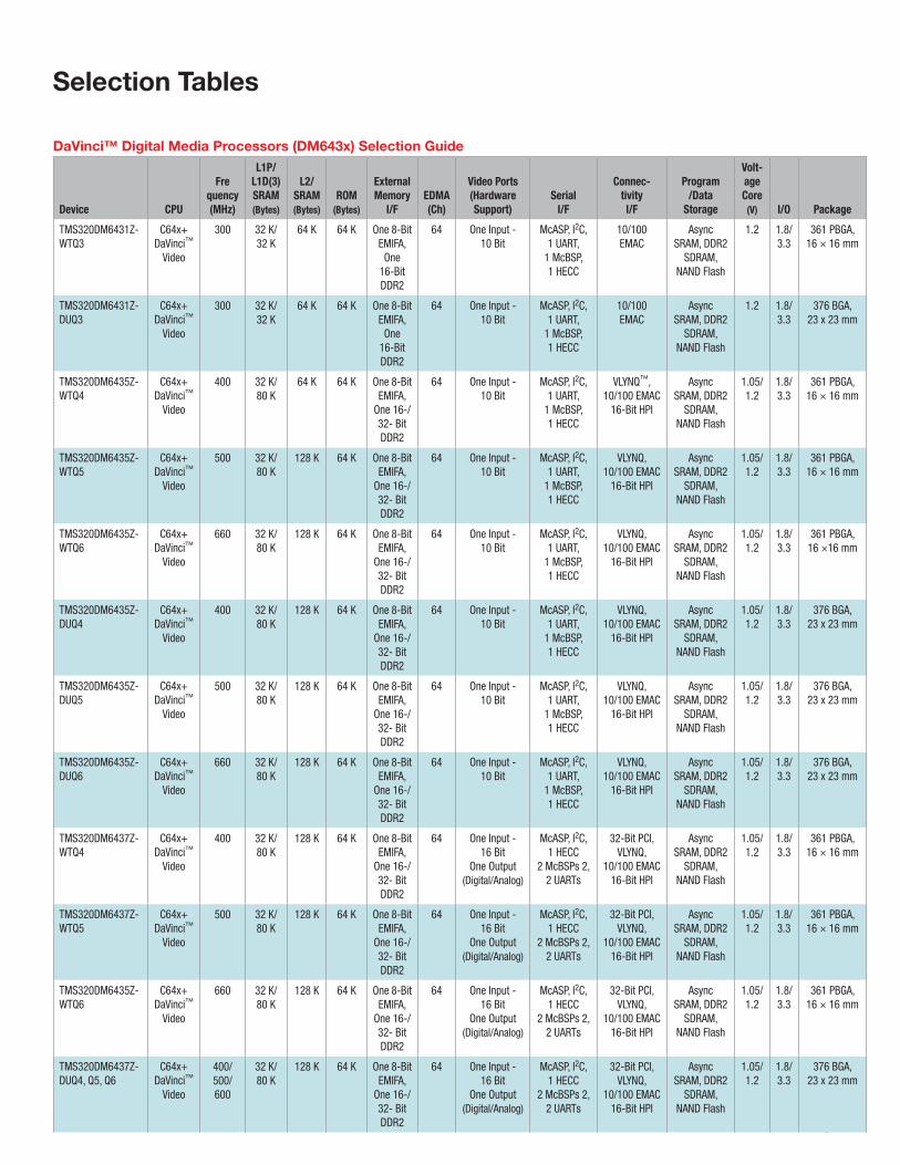
DaVinci™ Digital Media Processors (DM643x) Selection Guide
Device CPU
Frequency(MHz)
L1P/L1D(3)SRAM(Bytes)
L2/SRAM(Bytes)
ROM(Bytes)
ExternalMemory
I/FEDMA(Ch)
Video Ports (Hardware Support)
SerialI/F
Connec-tivityI/F
Program/Data
Storage
Volt-ageCore
(V) I/O Package
TMS320DM6431Z- WTQ3
C64x+DaVinci™
Video
300 32 K/32 K
64 K 64 K One 8-Bit EMIFA,
One 16-Bit DDR2
64 One Input - 10 Bit
McASP, I2C,1 UART,
1 McBSP,1 HECC
10/100 EMAC
Async SRAM, DDR2
SDRAM, NAND Flash
1.2 1.8/3.3
361 PBGA,16 × 16 mm
TMS320DM6431Z- DUQ3
C64x+DaVinci™
Video
300 32 K/32 K
64 K 64 K One 8-Bit EMIFA,
One 16-Bit DDR2
64 One Input - 10 Bit
McASP, I2C,1 UART,
1 McBSP,1 HECC
10/100 EMAC
Async SRAM, DDR2
SDRAM, NAND Flash
1.2 1.8/3.3
376 BGA,23 x 23 mm
TMS320DM6435Z- WTQ4
C64x+DaVinci™
Video
400 32 K/80 K
64 K 64 K One 8-Bit EMIFA,
One 16-/32- BitDDR2
64 One Input - 10 Bit
McASP, I2C,1 UART,
1 McBSP,1 HECC
VLYNQ™,10/100 EMAC
16-Bit HPI
Async SRAM, DDR2
SDRAM, NAND Flash
1.05/1.2
1.8/3.3
361 PBGA,16 × 16 mm
TMS320DM6435Z- WTQ5
C64x+DaVinci™
Video
500 32 K/80 K
128 K 64 K One 8-Bit EMIFA,
One 16-/32- BitDDR2
64 One Input - 10 Bit
McASP, I2C,1 UART,
1 McBSP,1 HECC
VLYNQ,10/100 EMAC
16-Bit HPI
Async SRAM, DDR2
SDRAM, NAND Flash
1.05/1.2
1.8/3.3
361 PBGA,16 × 16 mm
TMS320DM6435Z- WTQ6
C64x+DaVinci™
Video
660 32 K/80 K
128 K 64 K One 8-Bit EMIFA,
One 16-/32- BitDDR2
64 One Input - 10 Bit
McASP, I2C,1 UART,
1 McBSP,1 HECC
VLYNQ,10/100 EMAC
16-Bit HPI
Async SRAM, DDR2
SDRAM, NAND Flash
1.05/1.2
1.8/3.3
361 PBGA,16 ×16 mm
TMS320DM6435Z- DUQ4
C64x+DaVinci™
Video
400 32 K/80 K
128 K 64 K One 8-Bit EMIFA,
One 16-/32- BitDDR2
64 One Input - 10 Bit
McASP, I2C,1 UART,
1 McBSP,1 HECC
VLYNQ,10/100 EMAC
16-Bit HPI
Async SRAM, DDR2
SDRAM, NAND Flash
1.05/1.2
1.8/3.3
376 BGA,23 x 23 mm
TMS320DM6435Z- DUQ5
C64x+DaVinci™
Video
500 32 K/80 K
128 K 64 K One 8-Bit EMIFA,
One 16-/32- BitDDR2
64 One Input - 10 Bit
McASP, I2C,1 UART,
1 McBSP,1 HECC
VLYNQ,10/100 EMAC
16-Bit HPI
Async SRAM, DDR2
SDRAM, NAND Flash
1.05/1.2
1.8/3.3
376 BGA,23 x 23 mm
TMS320DM6435Z-DUQ6
C64x+DaVinci™
Video
660 32 K/80 K
128 K 64 K One 8-Bit EMIFA,
One 16-/32- BitDDR2
64 One Input - 10 Bit
McASP, I2C,1 UART,
1 McBSP,1 HECC
VLYNQ,10/100 EMAC
16-Bit HPI
Async SRAM, DDR2
SDRAM, NAND Flash
1.05/1.2
1.8/3.3
376 BGA,23 x 23 mm
TMS320DM6437Z- WTQ4
C64x+DaVinci™
Video
400 32 K/80 K
128 K 64 K One 8-Bit EMIFA,
One 16-/32- BitDDR2
64 One Input - 16 Bit
One Output(Digital/Analog)
McASP, I2C,1 HECC
2 McBSPs 2,2 UARTs
32-Bit PCI, VLYNQ,
10/100 EMAC16-Bit HPI
Async SRAM, DDR2
SDRAM, NAND Flash
1.05/1.2
1.8/3.3
361 PBGA,16 × 16 mm
TMS320DM6437Z- WTQ5
C64x+DaVinci™
Video
500 32 K/80 K
128 K 64 K One 8-Bit EMIFA,
One 16-/32- BitDDR2
64 One Input - 16 Bit
One Output(Digital/Analog)
McASP, I2C,1 HECC
2 McBSPs 2,2 UARTs
32-Bit PCI, VLYNQ,
10/100 EMAC16-Bit HPI
Async SRAM, DDR2
SDRAM, NAND Flash
1.05/1.2
1.8/3.3
361 PBGA,16 × 16 mm
TMS320DM6435Z- WTQ6
C64x+DaVinci™
Video
660 32 K/80 K
128 K 64 K One 8-Bit EMIFA,
One 16-/32- BitDDR2
64 One Input - 16 Bit
One Output(Digital/Analog)
McASP, I2C,1 HECC
2 McBSPs 2,2 UARTs
32-Bit PCI, VLYNQ,
10/100 EMAC16-Bit HPI
Async SRAM, DDR2
SDRAM, NAND Flash
1.05/1.2
1.8/3.3
361 PBGA,16 × 16 mm
TMS320DM6437Z- DUQ4, Q5, Q6
C64x+DaVinci™
Video
400/500/600
32 K/80 K
128 K 64 K One 8-Bit EMIFA,
One 16-/32- BitDDR2
64 One Input - 16 Bit
One Output(Digital/Analog)
McASP, I2C,1 HECC
2 McBSPs 2,2 UARTs
32-Bit PCI, VLYNQ,
10/100 EMAC16-Bit HPI
Async SRAM, DDR2
SDRAM, NAND Flash
1.05/1.2
1.8/3.3
376 BGA,23 x 23 mm
Selection Tables
26 | Advanced Driver Assistance Systems (ADAS) Guide 2013 Texas Instruments
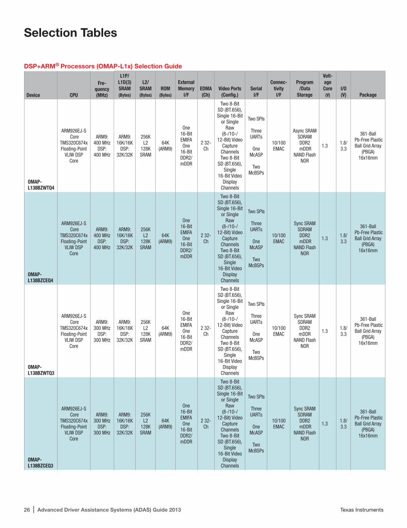
DSP+ARM® Processors (OMAP-L1x) Selection Guide
Device CPU
Fre-quency(MHz)
L1P/L1D(3)SRAM(Bytes)
L2/SRAM(Bytes)
ROM(Bytes)
ExternalMemory
I/FEDMA(Ch)
Video Ports (Config.)
SerialI/F
Connec-tivityI/F
Program/Data
Storage
Volt-ageCore
(V)I/O(V) Package
OMAP- L138BZWTQ4
ARM926EJ-S Core
TMS320C674x Floating-Point
VLIW DSP Core
ARM9:400 MHz
DSP:400 MHz
ARM9:16K/16K
DSP:32K/32K
256K L2
128K SRAM
64K (ARM9)
One 16-BitEMIFAOne
16-BitDDR2/mDDR
2 32- Ch
Two 8-Bit SD (BT.656), Single 16-Bit
or Single Raw
(8-/10-/12-Bit) Video
Capture Channels Two 8-Bit
SD (BT.656), Single
16-Bit Video Display
Channels
Two SPIs
ThreeUARTs
One McASP
TwoMcBSPs
10/100 EMAC
Async SRAM SDRAM DDR2
mDDRNAND Flash
NOR
1.3 1.8/3.3
361-Ball Pb-Free Plastic Ball Grid Array
(PBGA)16x16mm
OMAP- L138BZCEQ4
ARM926EJ-S Core
TMS320C674x Floating-Point
VLIW DSP Core
ARM9:400 MHz
DSP:400 MHz
ARM9:16K/16K
DSP:32K/32K
256K L2
128K SRAM
64K (ARM9)
One 16-BitEMIFAOne
16-BitDDR2/mDDR
2 32- Ch
Two 8-Bit SD (BT.656), Single 16-Bit
or Single Raw
(8-/10-/12-Bit) Video
Capture Channels Two 8-Bit
SD (BT.656), Single
16-Bit Video Display
Channels
Two SPIs
ThreeUARTs
One McASP
TwoMcBSPs
10/100 EMAC
Sync SRAM SDRAM DDR2
mDDRNAND Flash
NOR
1.3 1.8/3.3
361-Ball Pb-Free Plastic Ball Grid Array
(PBGA)16x16mm
OMAP- L138BZWTQ3
ARM926EJ-S Core
TMS320C674x Floating-Point
VLIW DSP Core
ARM9:300 MHz
DSP:300 MHz
ARM9:16K/16K
DSP:32K/32K
256K L2
128K SRAM
64K (ARM9)
One 16-BitEMIFAOne
16-BitDDR2/mDDR
2 32- Ch
Two 8-Bit SD (BT.656), Single 16-Bit
or Single Raw
(8-/10-/12-Bit) Video
Capture Channels Two 8-Bit
SD (BT.656), Single
16-Bit Video Display
Channels
Two SPIs
ThreeUARTs
One McASP
TwoMcBSPs
10/100 EMAC
Sync SRAM SDRAM DDR2 mDDR
NAND FlashNOR
1.3 1.8/3.3
361-Ball Pb-Free Plastic Ball Grid Array
(PBGA)16x16mm
OMAP- L138BZCEQ3
ARM926EJ-S Core
TMS320C674x Floating-Point
VLIW DSP Core
ARM9:300 MHz
DSP:300 MHz
ARM9:16K/16K
DSP:32K/32K
256K L2
128K SRAM
64K (ARM9)
One 16-BitEMIFAOne
16-BitDDR2/mDDR
2 32- Ch
Two 8-Bit SD (BT.656), Single 16-Bit
or Single Raw
(8-/10-/12-Bit) Video
Capture Channels Two 8-Bit
SD (BT.656), Single
16-Bit Video Display
Channels
Two SPIs
ThreeUARTs
One McASP
TwoMcBSPs
10/100 EMAC
Sync SRAM SDRAM DDR2
mDDRNAND Flash
NOR
1.3 1.8/3.3
361-Ball Pb-Free Plastic Ball Grid Array
(PBGA)16x16mm
Selection Tables

Texas Instruments Advanced Driver Assistance Systems (ADAS) Guide 2013 | 27
© 2013 Texas Instruments IncorporatedPrinted in U.S.A. by (Printer, City, State) SLYY044
TI Worldwide Technical Support
InternetTI Semiconductor Product Information Center Home Pagesupport.ti.com
TI E2E Community Home Pagee2e.ti.com
Product Information CentersAmericas Phone +1(512) 434-1560
Brazil Phone 0800-891-2616
Mexico Phone 0800-670-7544
Fax +1(972) 927-6377 Internet/Email support.ti.com/sc/pic/americas.htm
Europe, Middle East and AfricaPhone European Free Call 00800-ASK-TEXAS (00800 275 83927) International +49 (0) 8161 80 2121 Russian Support +7 (4) 95 98 10 701
Note: The European Free Call (Toll Free) number is not active in all countries. If you have technical difficulty calling the free call number, please use the international number above.
Fax +(49) (0) 8161 80 2045Internet www.ti.com/asktexasDirect Email [email protected]
JapanPhone Domestic 0120-92-3326
Fax International +81-3-3344-5317 Domestic 0120-81-0036
Internet/Email International support.ti.com/sc/pic/japan.htm Domestic www.tij.co.jp/pic
AsiaPhone International +91-80-41381665 Domestic Toll-Free Number Note: Toll-free numbers do not support
mobile and IP phones. Australia 1-800-999-084 China 800-820-8682 Hong Kong 800-96-5941 India 1-800-425-7888 Indonesia 001-803-8861-1006 Korea 080-551-2804 Malaysia 1-800-80-3973 New Zealand 0800-446-934 Philippines 1-800-765-7404 Singapore 800-886-1028 Taiwan 0800-006800 Thailand 001-800-886-0010Fax +8621-23073686Email [email protected] or [email protected] support.ti.com/sc/pic/asia.htm
A090712
Important Notice: The products and services of Texas Instruments Incorporated and its subsidiaries described herein are sold subject to TI’s standard terms and conditions of sale. Customers are advised to obtain the most current and complete information about TI products and services before placing orders. TI assumes no liability for applications assistance, customer’s applications or product designs, software performance, or infringement of patents. The publication of information regarding any other company’s products or services does not constitute TI’s approval, warranty or endorsement thereof.
TThe platform bar is a trademark of Texas Instruments. ARM and Cortex are registered trademarks of ARM Ltd. or its subsidiaries. All other trademarks are the property of their respective owners.
IMPORTANT NOTICE
Texas Instruments Incorporated and its subsidiaries (TI) reserve the right to make corrections, enhancements, improvements and otherchanges to its semiconductor products and services per JESD46, latest issue, and to discontinue any product or service per JESD48, latestissue. Buyers should obtain the latest relevant information before placing orders and should verify that such information is current andcomplete. All semiconductor products (also referred to herein as “components”) are sold subject to TI’s terms and conditions of salesupplied at the time of order acknowledgment.
TI warrants performance of its components to the specifications applicable at the time of sale, in accordance with the warranty in TI’s termsand conditions of sale of semiconductor products. Testing and other quality control techniques are used to the extent TI deems necessaryto support this warranty. Except where mandated by applicable law, testing of all parameters of each component is not necessarilyperformed.
TI assumes no liability for applications assistance or the design of Buyers’ products. Buyers are responsible for their products andapplications using TI components. To minimize the risks associated with Buyers’ products and applications, Buyers should provideadequate design and operating safeguards.
TI does not warrant or represent that any license, either express or implied, is granted under any patent right, copyright, mask work right, orother intellectual property right relating to any combination, machine, or process in which TI components or services are used. Informationpublished by TI regarding third-party products or services does not constitute a license to use such products or services or a warranty orendorsement thereof. Use of such information may require a license from a third party under the patents or other intellectual property of thethird party, or a license from TI under the patents or other intellectual property of TI.
Reproduction of significant portions of TI information in TI data books or data sheets is permissible only if reproduction is without alterationand is accompanied by all associated warranties, conditions, limitations, and notices. TI is not responsible or liable for such altereddocumentation. Information of third parties may be subject to additional restrictions.
Resale of TI components or services with statements different from or beyond the parameters stated by TI for that component or servicevoids all express and any implied warranties for the associated TI component or service and is an unfair and deceptive business practice.TI is not responsible or liable for any such statements.
Buyer acknowledges and agrees that it is solely responsible for compliance with all legal, regulatory and safety-related requirementsconcerning its products, and any use of TI components in its applications, notwithstanding any applications-related information or supportthat may be provided by TI. Buyer represents and agrees that it has all the necessary expertise to create and implement safeguards whichanticipate dangerous consequences of failures, monitor failures and their consequences, lessen the likelihood of failures that might causeharm and take appropriate remedial actions. Buyer will fully indemnify TI and its representatives against any damages arising out of the useof any TI components in safety-critical applications.
In some cases, TI components may be promoted specifically to facilitate safety-related applications. With such components, TI’s goal is tohelp enable customers to design and create their own end-product solutions that meet applicable functional safety standards andrequirements. Nonetheless, such components are subject to these terms.
No TI components are authorized for use in FDA Class III (or similar life-critical medical equipment) unless authorized officers of the partieshave executed a special agreement specifically governing such use.
Only those TI components which TI has specifically designated as military grade or “enhanced plastic” are designed and intended for use inmilitary/aerospace applications or environments. Buyer acknowledges and agrees that any military or aerospace use of TI componentswhich have not been so designated is solely at the Buyer's risk, and that Buyer is solely responsible for compliance with all legal andregulatory requirements in connection with such use.
TI has specifically designated certain components as meeting ISO/TS16949 requirements, mainly for automotive use. In any case of use ofnon-designated products, TI will not be responsible for any failure to meet ISO/TS16949.
Products Applications
Audio www.ti.com/audio Automotive and Transportation www.ti.com/automotive
Amplifiers amplifier.ti.com Communications and Telecom www.ti.com/communications
Data Converters dataconverter.ti.com Computers and Peripherals www.ti.com/computers
DLP® Products www.dlp.com Consumer Electronics www.ti.com/consumer-apps
DSP dsp.ti.com Energy and Lighting www.ti.com/energy
Clocks and Timers www.ti.com/clocks Industrial www.ti.com/industrial
Interface interface.ti.com Medical www.ti.com/medical
Logic logic.ti.com Security www.ti.com/security
Power Mgmt power.ti.com Space, Avionics and Defense www.ti.com/space-avionics-defense
Microcontrollers microcontroller.ti.com Video and Imaging www.ti.com/video
RFID www.ti-rfid.com
OMAP Applications Processors www.ti.com/omap TI E2E Community e2e.ti.com
Wireless Connectivity www.ti.com/wirelessconnectivity
Mailing Address: Texas Instruments, Post Office Box 655303, Dallas, Texas 75265Copyright © 2013, Texas Instruments Incorporated