Embed Size (px)
Citation preview

Smart GaN-Based Inverters forGrid-tied Energy Storage Systems
DOE OE Peer Review, September 2020
1
Innovation City, Power and Energy Solutions
DOE SBIR Phase IIB
Year 1 start date: 08/19/2019
Year 1 end date: 08/18/2020

AcknowledgementInnoCit greatly appreciates support of Dr. Imre Gyuk and Dr. Stan Atcitty through DOE SBIR grant DE-SC0013818.
2
• Founded in 2014
• Tech Transfer Startup
• 4,000 sq. ft. research facility, 10 acre campus, solar farm, based in Missouri
• DOE SBIR Phase I, II, IIB, NSF SBIR Phase I
• Costume manufacturing
3
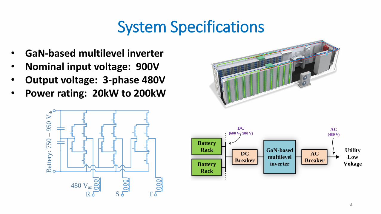
Battery
Rack
Battery
Rack
DC
Breaker
GaN-based
multilevel
inverter
AC
Breaker
Utility
Low
Voltage
DC(600 V~ 900 V)
AC(480 V)
480 Vac
Bat
tery
: 7
50
– 9
50
Vdc
R S T
System Specifications
• GaN-based multilevel inverter• Nominal input voltage: 900V• Output voltage: 3-phase 480V• Power rating: 20kW to 200kW

4
Specific Objectives
• Designing 3U rack-chassis-based enclosures for inverter modules• Conduct thermal analysis on the enclosures• Controls and hardware for hot-swap capabilities• Validate final metrics: efficiency of at least 98.6%, weight < 2.2 lb./kW,
volume <0.1 ft3/kW, noise <45 dBa• Reliability testing including active bypass and hot-swap features• IEEE 1547, UL 1741, and 1741-SA testing for islanding and fault ride-
through• UL certification testing• Remote control and monitoring backbone structure development

Fast-Paced Technology
5
Technology / manufacturer Transphorm EPC GaN systems GaN systems
Switch topology Cascode: GaN JFET + Si
MOSFET
Enhancement mode FET Enhancement mode FET Enhancement mode FET
Material GaN + Si GaN GaN GaN
Part number TPH3205WS EPC2034 GS66508T GS66516T
Voltage 600 V 200 V 650 V 650 V
Current 36 A 31 A 30 A 60 A
Rds-on @ 150 ̊C 0.10 Ω 0.015 Ω 0.050 Ω 0.025 Ω
CRSS (Reverse transfer) 17.5 pF 5 pF 2 pF 4 pF
Heatsink Plate no Yes Yes
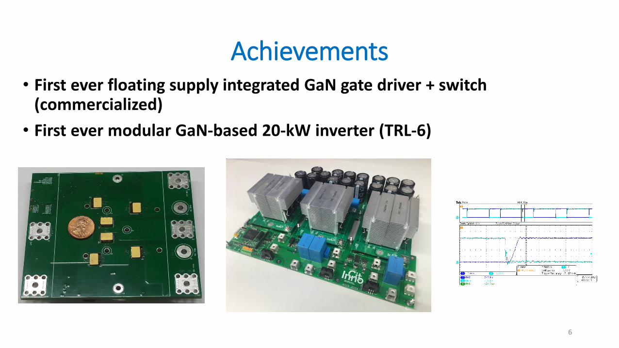
Achievements
6
• First ever floating supply integrated GaN gate driver + switch (commercialized)
• First ever modular GaN-based 20-kW inverter (TRL-6)

Switch Reliability
7
• Soldering tolerance

Bottom-Cooled GaN Switch
8
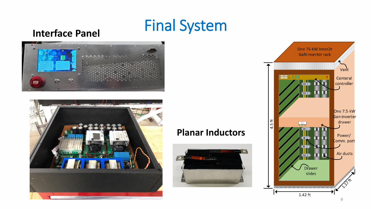
Final System
9
Planar Inductors
Interface Panel
Intelligent Inverter
10
+
+−
−
1
S
Pset
Pout
ResetPower
Iabc
Vabc
Optimization
Pset
Pout
Qout
Data preparation
Pout
Qout
Neural Network Model
E
setP
setQ
pY
refY
pD
i
i
i
i 1
S
1
iJ
g
nnY
Fault Detection & Control ler
Selection Unit
Iabc
Vabc

Commercial Competitiveness
11
Features\Manufacturer InnoCitGanverter (10 units)
Princeton PowerBIGI-250
ABBESSpro-C250
DynaPowerMPS-100
Total Power Rating (S) 200-kVA 265-kVA 200-kVA 100-kVA
CEC Efficiency 99% 94.5% >94% 93.9%
Volume 30-ft3 (full system + rack)
150-ft3 41-ft3 48-ft3
Weight 540-lbs. (full system + rack)
3500-lbs. 2100-lbs. 1545-lbs.
Current THD <2% <5% <5% <5%
End-user Price per VA $0.085/VA $0.44/VA $0.58/VA $0.52/VA

Lessons Learned
• Gate driver design is very critical
• Requires isolated gate drivers and isolated dc-dc power supplies fordriving the gate
• When selecting the isolated gate driver and gate power supply, oneshould ensure that they can withstand the high dv/dt stress due tofaster turn ON and OFF times
• With the fast switching of GaN E-HEMTs, any parasitic inductances inthe gate switching loop will give rise to ringing which leads to lossesand EMI problems - keep the PCB gate-source loop as small aspossible
• Best switching performance can be achieved with proper selection ofgate resistor
Lessons Learned
• Poor thermal conductivity of GaN semiconductor calls for special attention to thermal design
• GaN E-HEMTs have tiny packaging compared to SiC. Therefore, the heat generated within the device has to be dissipated fast and effectively to keep the junction temperature within allowable limits
• Also, the maximum junction temperature of the GaN E-HEMT selected is low compared to the SiC device
• If using a single heat sink for multiple GaN devices, they have to be aligned flat with the surface of heat sink
• Using thermal grease along with thermal tape will provide the best thermal conductivity