Embed Size (px)
Citation preview
Product
Folder
Order
Now
Technical
Documents
Tools &
Software
Support &Community
An IMPORTANT NOTICE at the end of this data sheet addresses availability, warranty, changes, use in safety-critical applications,intellectual property matters and other important disclaimers. PRODUCTION DATA.
LM3102SNVS515I –SEPTEMBER 2007–REVISED JANUARY 2018
LM3102 Synchronous 1-MHz, 2.5-A Step-Down Voltage Regulator
1
1 Features1• Low Component Count and Small Solution Size• Stable With Ceramic and Other Low-ESR
Capacitors• No Loop Compensation Required• High Efficiency at a Light Load by DCM Operation• Prebias Start-Up• Ultra-Fast Transient Response• Programmable Soft-Start• Programmable Switching Frequency up to 1 MHz• Valley Current Limit• Output Overvoltage Protection• Precision Internal Reference for an Adjustable
Output Voltage Down to 0.8 V• Thermal Shutdown• Key Specifications
– Input Voltage Range 4.5 V to 42 V– 2.5-A Output Current– 0.8 V, ±1.5% Reference– Integrated Dual N-Channel Main and
Synchronous MOSFETs– Thermally Enhanced HTSSOP-20 Package
2 Applications• 5-VDC, 12-VDC, 24-VDC, 12-VAC, and 24-VAC
Systems• Embedded Systems and Industrial Control• Automotive Telematics and Body Electronics• Point of Load Regulators
• Storage Systems• Broadband Infrastructure• Direct Conversion from 2-, 3-, and 4-Cell Lithium
Batteries Systems
3 DescriptionThe LM3102 Synchronously Rectified Buck Converterfeatures all required functions to implement a highlyefficient and cost-effective buck regulator. The devicecan supply 2.5 A to loads with an output voltage aslow as 0.8 V. Dual N-channel synchronous MOSFETswitches allow a low component count, thus reducingcomplexity and minimizing board size.
Different from most other COT regulators, theLM3102 does not rely on output capacitor ESR forstability, and is designed to work exceptionally wellwith ceramic and other very low-ESR outputcapacitors. The device requires no loopcompensation, results in a fast load transientresponse and simple circuit implementation. Theoperating frequency remains nearly constant with linevariations due to the inverse relationship between theinput voltage and the ON-time. The operatingfrequency can be externally programmed up to1 MHz. Protection features include VCC undervoltagelockout (UVLO), output overvoltage protection,thermal shutdown, and gate drive UVLO. TheLM3102 is available in the thermally enhancedHTSSOP-20 package, and LM3102 is also availablein a DSBGA low-profile chip-scale package withreduced output current.
Device Information(1)
PART NUMBER PACKAGE BODY SIZE (NOM)LM3102 DSBGA (28) 3.645 mm × 2.45 mmLM3102 HTSSOP (20) 6.50 mm × 4.40 mm
(1) For all available packages, see the orderable addendum atthe end of the data sheet.
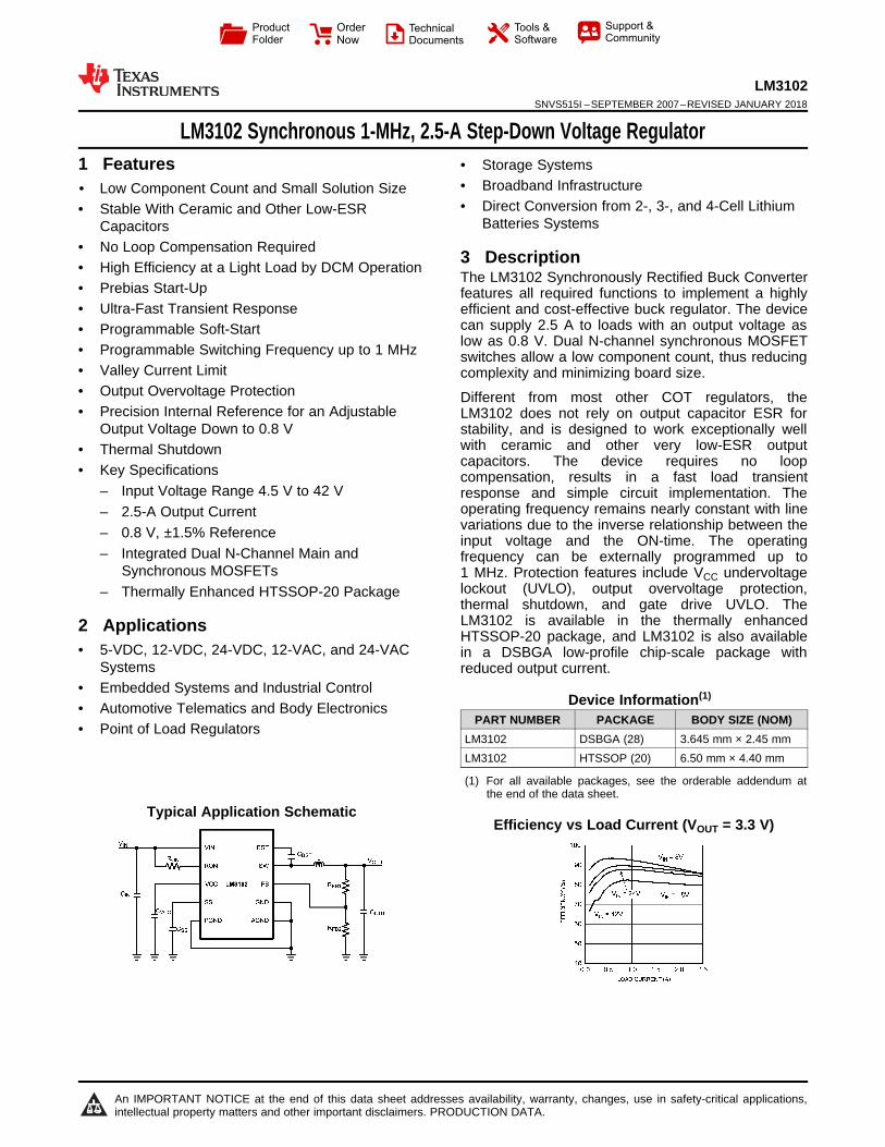
Typical Application SchematicEfficiency vs Load Current (VOUT = 3.3 V)
2
LM3102SNVS515I –SEPTEMBER 2007–REVISED JANUARY 2018 www.ti.com
Product Folder Links: LM3102
Submit Documentation Feedback Copyright © 2007–2018, Texas Instruments Incorporated
Table of Contents1 Features .................................................................. 12 Applications ........................................................... 13 Description ............................................................. 14 Revision History..................................................... 25 Pin Configuration and Functions ......................... 36 Specifications......................................................... 4
6.1 Absolute Maximum Ratings ...................................... 46.2 ESD Ratings.............................................................. 46.3 Recommended Operating Conditions....................... 46.4 Thermal Information .................................................. 46.5 Electrical Characteristics........................................... 56.6 Typical Characteristics .............................................. 7
7 Detailed Description ............................................ 117.1 Overview ................................................................. 117.2 Functional Block Diagram ....................................... 117.3 Feature Description................................................. 11
7.4 Device Functional Modes........................................ 148 Application and Implementation ........................ 16
8.1 Application Information............................................ 168.2 Typical Application .................................................. 168.3 System Examples ................................................... 20
9 Power Supply Recommendations ...................... 2110 Layout................................................................... 21
10.1 Layout Guidelines ................................................. 2110.2 Layout Example .................................................... 21
11 Device and Documentation Support ................. 2311.1 Community Resources.......................................... 2311.2 Trademarks ........................................................... 2311.3 Electrostatic Discharge Caution............................ 2311.4 Glossary ................................................................ 23
12 Mechanical, Packaging, and OrderableInformation ........................................................... 23
4 Revision HistoryNOTE: Page numbers for previous revisions may differ from page numbers in the current version.
Changes from Revision H (June 2015) to Revision I Page
• Changed LM3102 and LM3102-Q1 to Stand Alone data sheets .......................................................................................... 1
Changes from Revision G (January 2012) to Revision H Page
• Updated the LM3102Q part number to LM3102-Q1 ............................................................................................................. 1• Added Pin Configuration and Functions section, ESD Ratings table, Feature Description section, Device Functional
Modes, Application and Implementation section, Power Supply Recommendations section, Layout section, Deviceand Documentation Support section, and Mechanical, Packaging, and Orderable Information section .............................. 1

VIN VIN BST SW AGND RON EN
SW SW SW SW AGND AGND AGND
SW SW SW SW VCC AGND SS
PGND PGND PGND VCC AGND FB
A B C D E F G
4
3
2
1 PGND
Top Mark
3
LM3102www.ti.com SNVS515I –SEPTEMBER 2007–REVISED JANUARY 2018
Product Folder Links: LM3102
Submit Documentation FeedbackCopyright © 2007–2018, Texas Instruments Incorporated
5 Pin Configuration and Functions
PWP Package20-Pin HTSSOP
Top ViewYPA Package
28–Ball DSBGATop View
Pin FunctionsPIN
TYPE DESCRIPTIONNAME PIN NO. BALL NO.
N/C
1
— — No Connection
910121920
SW
2
A2
Power Switching Node
A3B2B3C2
3
C3D2D3D4
VIN4 A4
Power Input supply voltage5 B4
BST 6 C4 Power Connection for bootstrap capacitor
AGND 7
E3
Ground Analog Ground
E4F1F2F3G3
SS 8 G2 Analog Soft-StartGND 11 — Ground GroundFB 13 G1 Analog FeedbackEN 14 G4 Analog EnableRON 15 F4 Analog ON-time Control
VCC 16E1
Power Start-up regulator OutputE2
4
LM3102SNVS515I –SEPTEMBER 2007–REVISED JANUARY 2018 www.ti.com
Product Folder Links: LM3102
Submit Documentation Feedback Copyright © 2007–2018, Texas Instruments Incorporated
Pin Functions (continued)PIN
TYPE DESCRIPTIONNAME PIN NO. BALL NO.
PGND17
A1
Ground Power GroundB1
18C1D1
EP EP — Ground Exposed Pad
(1) Stresses beyond those listed under Absolute Maximum Ratings may cause permanent damage to the device. These are stress ratingsonly, which do not imply functional operation of the device at these or any other conditions beyond those indicated under RecommendedOperating Conditions. Exposure to absolute-maximum-rated conditions for extended periods may affect device reliability.
6 Specifications
6.1 Absolute Maximum Ratingsover operating free-air temperature range (unless otherwise noted) (1)
MIN MAX UNITVIN, RON to AGND –0.3 43.5 VSW to AGND –0.3 43.5 VSW to AGND (Transient) –2 (< 100 ns) VVIN to SW –0.3 43.5 VBST to SW –0.3 7 VAll Other Inputs to AGND –0.3 7 VJunction Temperature, TJ 150 °CStorage Temperature, Tstg –65 150 °C
(1) JEDEC document JEP155 states that 500-V HBM allows safe manufacturing with a standard ESD control process.
6.2 ESD RatingsVALUE UNIT
V(ESD) Electrostatic discharge Human body model (HBM), per ANSI/ESDA/JEDEC JS-001 (1) ±2000 V
(1) Absolute Maximum Ratings are limits beyond which damage to the device may occur. Recommended Operating Ratings are conditionsunder which operation of the device is intended to be functional. For ensured specifications and test conditions, see the ElectricalCharacteristics.
6.3 Recommended Operating Conditionsover operating free-air temperature range (unless otherwise noted) (1)
MIN MAX UNITSupply Voltage Range (VIN) 4.5 42 VJunction Temperature Range (TJ) −40 125 °C
(1) For more information about traditional and new thermal metrics, see the Semiconductor and IC Package Thermal Metrics applicationreport, SPRA953.
6.4 Thermal Information
THERMAL METRIC (1)LM3102 LM3102
UNITPWP (HTSSOP) YPA (DSBGA)20 PINS 28 PINS
RθJA Junction-to-ambient thermal resistance 30 50 °C/WRθJC(top) Junction-to-case (top) thermal resistance 6.5 — °C/W
5
LM3102www.ti.com SNVS515I –SEPTEMBER 2007–REVISED JANUARY 2018
Product Folder Links: LM3102
Submit Documentation FeedbackCopyright © 2007–2018, Texas Instruments Incorporated
(1) VCC provides self bias for the internal gate drive and control circuits. Device thermal limitations limit external loading.
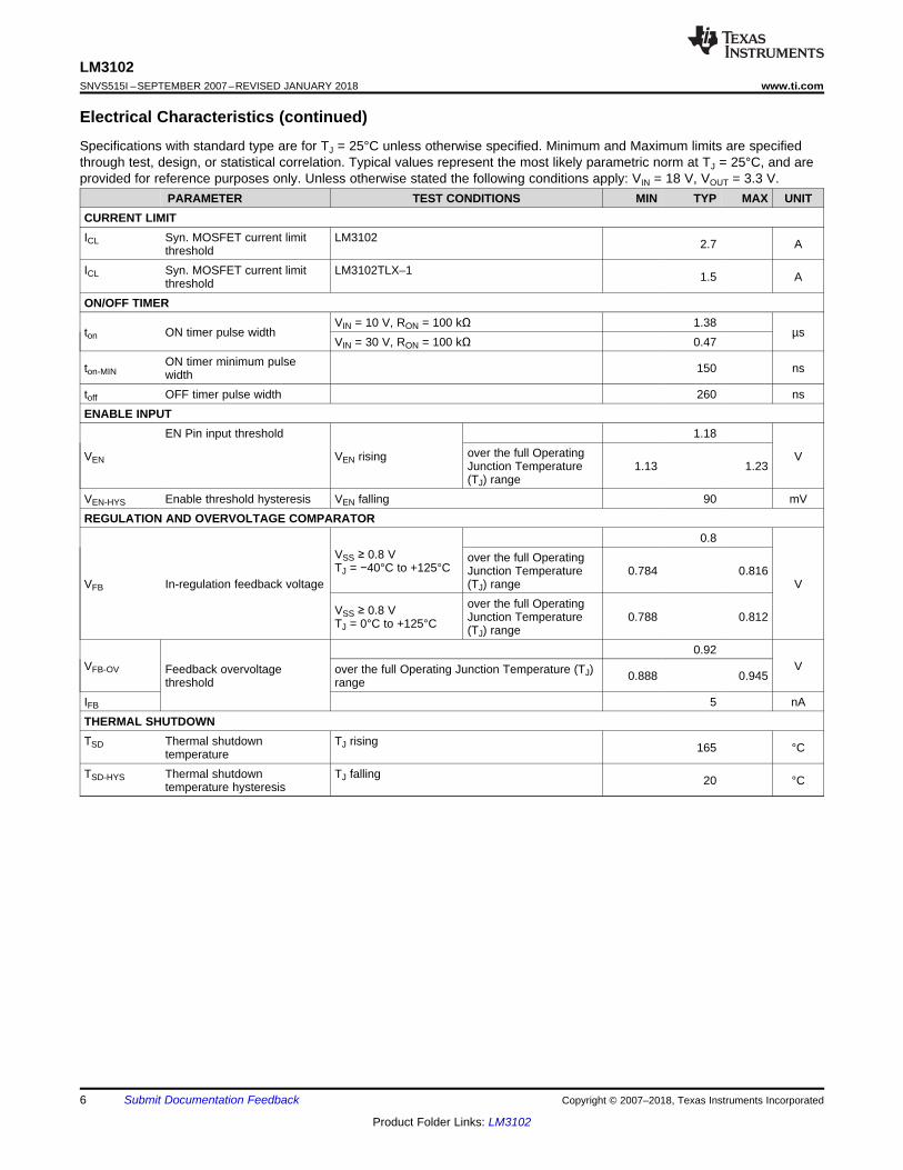
6.5 Electrical CharacteristicsSpecifications with standard type are for TJ = 25°C unless otherwise specified. Minimum and Maximum limits are specifiedthrough test, design, or statistical correlation. Typical values represent the most likely parametric norm at TJ = 25°C, and areprovided for reference purposes only. Unless otherwise stated the following conditions apply: VIN = 18 V, VOUT = 3.3 V.
PARAMETER TEST CONDITIONS MIN TYP MAX UNITSTART-UP REGULATOR, VCC
VCC VCC output voltage CCC = 680 nF, no load
6
Vover the full OperatingJunction Temperature(TJ) range
5 7.2
VIN – VCC VIN – VCC dropout voltage
ICC = 2 mA
50
mV
over the full OperatingJunction Temperature(TJ) range
200
ICC = 20 mA
350over the full OperatingJunction Temperature(TJ) range
570
IVCCL VCC current limit (1) VCC = 0 V
65
mAover the full OperatingJunction Temperature(TJ) range
40
VCC-UVLOVCC undervoltage lockoutthreshold (UVLO) VIN increasing
3.75
Vover the full OperatingJunction Temperature(TJ) range
3.6 3.9
VCC-UVLO-HYS VCC UVLO hysteresis VIN decreasing – HTSSOP package 130 mVVCC-UVLO-HYS VCC UVLO hysteresis VIN decreasing – DSBGA package 150 mVtVCC-UVLO-D VCC UVLO filter delay 3 µs
IIN IIN operating current No switching, VFB = 1V
0.7
mAover the full OperatingJunction Temperature(TJ) range
1
IIN-SDIIN operating current, Deviceshutdown VEN = 0 V
25
µAover the full OperatingJunction Temperature(TJ) range
40
SWITCHING CHARACTERISTICS
RDS-UP-ON Main MOSFET RDS(on)
0.18Ωover the full Operating Junction Temperature (TJ)
range 0.375
RDS- DN-ON Syn. MOSFET RDS(on)
0.11Ωover the full Operating Junction Temperature (TJ)
range 0.225
VG-UVLO Gate drive voltage UVLO VBST - VSW increasing
3.3
Vover the full OperatingJunction Temperature(TJ) range
4
SOFT-START
ISS SS pin source current VSS = 0.5 V
8
µAover the full OperatingJunction Temperature(TJ) range
6 10
6
LM3102SNVS515I –SEPTEMBER 2007–REVISED JANUARY 2018 www.ti.com
Product Folder Links: LM3102
Submit Documentation Feedback Copyright © 2007–2018, Texas Instruments Incorporated
Electrical Characteristics (continued)Specifications with standard type are for TJ = 25°C unless otherwise specified. Minimum and Maximum limits are specifiedthrough test, design, or statistical correlation. Typical values represent the most likely parametric norm at TJ = 25°C, and areprovided for reference purposes only. Unless otherwise stated the following conditions apply: VIN = 18 V, VOUT = 3.3 V.
PARAMETER TEST CONDITIONS MIN TYP MAX UNITCURRENT LIMITICL Syn. MOSFET current limit
thresholdLM3102 2.7 A
ICL Syn. MOSFET current limitthreshold
LM3102TLX–1 1.5 A
ON/OFF TIMER
ton ON timer pulse widthVIN = 10 V, RON = 100 kΩ 1.38
µsVIN = 30 V, RON = 100 kΩ 0.47
ton-MINON timer minimum pulsewidth 150 ns
toff OFF timer pulse width 260 nsENABLE INPUT
VEN
EN Pin input threshold
VEN rising
1.18
Vover the full OperatingJunction Temperature(TJ) range
1.13 1.23
VEN-HYS Enable threshold hysteresis VEN falling 90 mVREGULATION AND OVERVOLTAGE COMPARATOR
VFB In-regulation feedback voltage
VSS ≥ 0.8 VTJ = −40°C to +125°C
0.8
V
over the full OperatingJunction Temperature(TJ) range
0.784 0.816
VSS ≥ 0.8 VTJ = 0°C to +125°C
over the full OperatingJunction Temperature(TJ) range
0.788 0.812
VFB-OV Feedback overvoltagethreshold
0.92Vover the full Operating Junction Temperature (TJ)
range 0.888 0.945
IFB 5 nATHERMAL SHUTDOWNTSD Thermal shutdown
temperatureTJ rising 165 °C
TSD-HYS Thermal shutdowntemperature hysteresis
TJ falling 20 °C

7
LM3102www.ti.com SNVS515I –SEPTEMBER 2007–REVISED JANUARY 2018
Product Folder Links: LM3102
Submit Documentation FeedbackCopyright © 2007–2018, Texas Instruments Incorporated
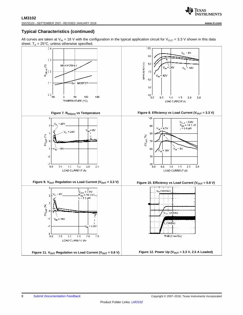
6.6 Typical CharacteristicsAll curves are taken at VIN = 18 V with the configuration in the typical application circuit for VOUT = 3.3 V shown in this datasheet. TA = 25°C, unless otherwise specified.
Figure 1. Quiescent Current, IIN vs VIN Figure 2. VCC vs ICC
Figure 3. VCC vs VIN Figure 4. ton vs VIN
Figure 5. Switching Frequency, fSW vs VIN Figure 6. VFB vs Temperature
8
LM3102SNVS515I –SEPTEMBER 2007–REVISED JANUARY 2018 www.ti.com
Product Folder Links: LM3102
Submit Documentation Feedback Copyright © 2007–2018, Texas Instruments Incorporated
Typical Characteristics (continued)All curves are taken at VIN = 18 V with the configuration in the typical application circuit for VOUT = 3.3 V shown in this datasheet. TA = 25°C, unless otherwise specified.
Figure 7. RDS(on) vs Temperature Figure 8. Efficiency vs Load Current (VOUT = 3.3 V)
Figure 9. VOUT Regulation vs Load Current (VOUT = 3.3 V) Figure 10. Efficiency vs Load Current (VOUT = 0.8 V)
Figure 11. VOUT Regulation vs Load Current (VOUT = 0.8 V) Figure 12. Power Up (VOUT = 3.3 V, 2.5 A Loaded)
9
LM3102www.ti.com SNVS515I –SEPTEMBER 2007–REVISED JANUARY 2018
Product Folder Links: LM3102
Submit Documentation FeedbackCopyright © 2007–2018, Texas Instruments Incorporated
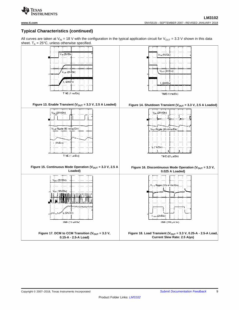
Typical Characteristics (continued)All curves are taken at VIN = 18 V with the configuration in the typical application circuit for VOUT = 3.3 V shown in this datasheet. TA = 25°C, unless otherwise specified.
Figure 13. Enable Transient (VOUT = 3.3 V, 2.5 A Loaded) Figure 14. Shutdown Transient (VOUT = 3.3 V, 2.5 A Loaded)
Figure 15. Continuous Mode Operation (VOUT = 3.3 V, 2.5 ALoaded)
Figure 16. Discontinuous Mode Operation (VOUT = 3.3 V,0.025 A Loaded)
Figure 17. DCM to CCM Transition (VOUT = 3.3 V,0.15-A - 2.5-A Load)
Figure 18. Load Transient (VOUT = 3.3 V, 0.25-A - 2.5-A Load,Current Slew Rate: 2.5 A/µs)
1.5
1.55
1.6
1.65
1.7
1.75
1.8
0 10 20 30 40 50
INPUT VOLTAGE (V)
VA
LLE
Y C
UR
RE
NT
LIM
IT (
A)
25°C
10
LM3102SNVS515I –SEPTEMBER 2007–REVISED JANUARY 2018 www.ti.com
Product Folder Links: LM3102
Submit Documentation Feedback Copyright © 2007–2018, Texas Instruments Incorporated
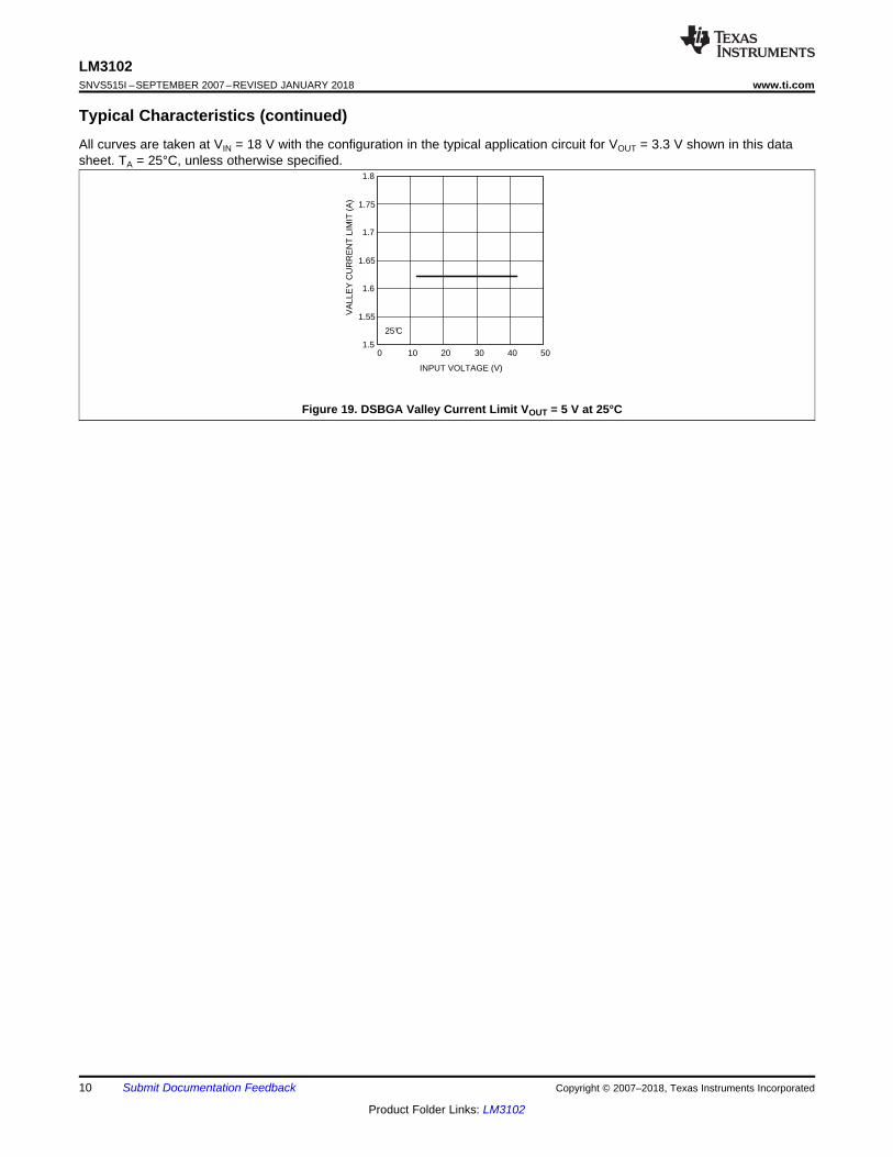
Typical Characteristics (continued)All curves are taken at VIN = 18 V with the configuration in the typical application circuit for VOUT = 3.3 V shown in this datasheet. TA = 25°C, unless otherwise specified.
Figure 19. DSBGA Valley Current Limit VOUT = 5 V at 25°C
11
LM3102www.ti.com SNVS515I –SEPTEMBER 2007–REVISED JANUARY 2018
Product Folder Links: LM3102
Submit Documentation FeedbackCopyright © 2007–2018, Texas Instruments Incorporated
7 Detailed Description
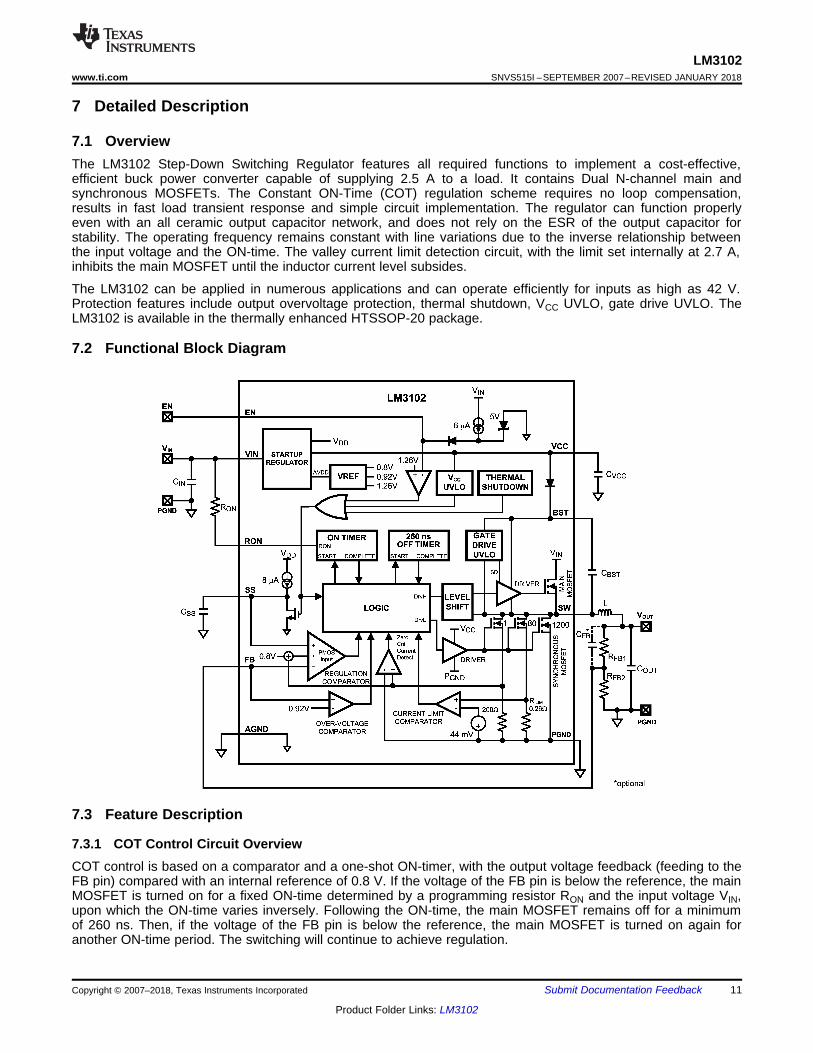
7.1 OverviewThe LM3102 Step-Down Switching Regulator features all required functions to implement a cost-effective,efficient buck power converter capable of supplying 2.5 A to a load. It contains Dual N-channel main andsynchronous MOSFETs. The Constant ON-Time (COT) regulation scheme requires no loop compensation,results in fast load transient response and simple circuit implementation. The regulator can function properlyeven with an all ceramic output capacitor network, and does not rely on the ESR of the output capacitor forstability. The operating frequency remains constant with line variations due to the inverse relationship betweenthe input voltage and the ON-time. The valley current limit detection circuit, with the limit set internally at 2.7 A,inhibits the main MOSFET until the inductor current level subsides.
The LM3102 can be applied in numerous applications and can operate efficiently for inputs as high as 42 V.Protection features include output overvoltage protection, thermal shutdown, VCC UVLO, gate drive UVLO. TheLM3102 is available in the thermally enhanced HTSSOP-20 package.
7.2 Functional Block Diagram
7.3 Feature Description
7.3.1 COT Control Circuit OverviewCOT control is based on a comparator and a one-shot ON-timer, with the output voltage feedback (feeding to theFB pin) compared with an internal reference of 0.8 V. If the voltage of the FB pin is below the reference, the mainMOSFET is turned on for a fixed ON-time determined by a programming resistor RON and the input voltage VIN,upon which the ON-time varies inversely. Following the ON-time, the main MOSFET remains off for a minimumof 260 ns. Then, if the voltage of the FB pin is below the reference, the main MOSFET is turned on again foranother ON-time period. The switching will continue to achieve regulation.
VOUT
1.3 x 10⁻¹⁰ x RONfSW =
(VIN ± VOUT) x RON2
VOUT (VIN - 1) x L x 1.18 x 10²⁰ x IOUTfSW =
12
LM3102SNVS515I –SEPTEMBER 2007–REVISED JANUARY 2018 www.ti.com
Product Folder Links: LM3102
Submit Documentation Feedback Copyright © 2007–2018, Texas Instruments Incorporated
Feature Description (continued)The regulator will operate in the discontinuous conduction mode (DCM) at a light load, and the continuousconduction mode (CCM) with a heavy load. In the DCM, the current through the inductor starts at zero andramps up to a peak during the ON-time, and then ramps back to zero before the end of the OFF-time. It remainszero and the load current is supplied entirely by the output capacitor. The next ON-time period starts when thevoltage at the FB pin falls below the internal reference. The operating frequency in the DCM is lower and varieslarger with the load current as compared with the CCM. Conversion efficiency is maintained because conductionloss and switching loss are reduced with the reduction in the load and the switching frequency, respectively. Theoperating frequency in the DCM can be calculated approximately as follows:
(1)
In the continuous conduction mode (CCM), the current flows through the inductor in the entire switching cycle,and never reaches zero during the OFF-time. The operating frequency remains relatively constant with load andline variations. The CCM operating frequency can be calculated approximately as follows:
(2)
The output voltage is set by two external resistors RFB1 and RFB2. The regulated output voltage isVOUT = 0.8V x (RFB1 + RFB2)/RFB2 (3)
7.3.2 Start-Up Regulator (VCC)A startup regulator is integrated within the LM3102. The input pin VIN can be connected directly to a line voltageup to 42 V. The VCC output regulates at 6 V, and is current limited to 65 mA. Upon power up, the regulatorsources current into an external capacitor CVCC, which is connected to the VCC pin. For stability, CVCC must be atleast 680 nF. When the voltage on the VCC pin is higher than the UVLO threshold of 3.75 V, the main MOSFETis enabled and the SS pin is released to allow the soft-start capacitor CSS to charge.
The minimum input voltage is determined by the dropout voltage of the regulator and the VCC UVLO fallingthreshold (≊3.7 V). If VIN is less than ≊4.0 V, the regulator shuts off and VCC goes to zero.
7.3.3 Regulation ComparatorThe feedback voltage at the FB pin is compared to a 0.8-V internal reference. In normal operation (the outputvoltage is regulated), an ON-time period is initiated when the voltage at the FB pin falls below 0.8 V. The mainMOSFET stays on for the ON-time, causing the output voltage and consequently the voltage of the FB pin to riseabove 0.8 V. After the ON-time period, the main MOSFET stays off until the voltage of the FB pin falls below 0.8V again. Bias current at the FB pin is nominally 5 nA.
7.3.4 Zero Coil Current DetectThe current of the synchronous MOSFET is monitored by a zero coil current detection circuit which inhibits thesynchronous MOSFET when its current reaches zero until the next ON-time. This circuit enables the DCMoperation, which improves the efficiency at a light load.
7.3.5 Overvoltage ComparatorThe voltage at the FB pin is compared to a 0.92-V internal reference. If the voltage rises above 0.92 V, the ON-time is immediately terminated. This condition is known as overvoltage protection (OVP). It can occur if the inputvoltage or the output load changes suddenly. Once the OVP is activated, the main MOSFET remains off until thevoltage at the FB pin falls below 0.92 V. The synchronous MOSFET will stay on to discharge the inductor untilthe inductor current reduces to zero, and then switch off.
ILR =(VIN - VOUT) x ton
L
13
LM3102www.ti.com SNVS515I –SEPTEMBER 2007–REVISED JANUARY 2018
Product Folder Links: LM3102
Submit Documentation FeedbackCopyright © 2007–2018, Texas Instruments Incorporated
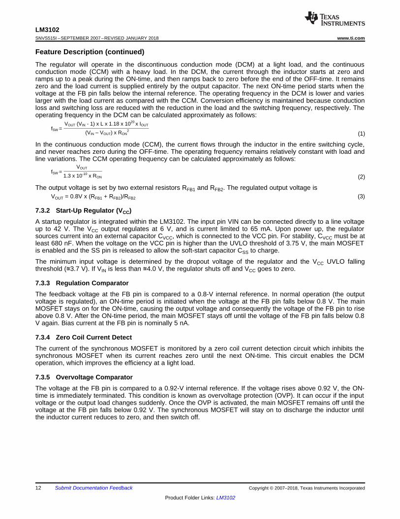
Feature Description (continued)7.3.6 Current LimitCurrent limit detection is carried out during the OFF-time by monitoring the re-circulating current through thesynchronous MOSFET. Referring to the Functional Block Diagram, when the main MOSFET is turned off, theinductor current flows through the load, the PGND pin and the internal synchronous MOSFET. If this currentexceeds 2.7 A, the current limit comparator toggles, and as a result disabling the start of the next ON-timeperiod. The next switching cycle starts when the re-circulating current falls back below 2.7 A (and the voltage atthe FB pin is below 0.8V). The inductor current is monitored during the ON-time of the synchronous MOSFET. Aslong as the inductor current exceeds 2.7 A, the main MOSFET will remain inhibited to achieve current limit. Theoperating frequency is lower during current limit due to a longer OFF-time.
Figure 20 illustrates an inductor current waveform. On average, the output current IOUT is the same as theinductor current IL, which is the average of the rippled inductor current. In case of current limit (the current limitportion of Figure 20), the next ON-time will not initiate until that the current drops below 2.7 A (assume thevoltage at the FB pin is lower than 0.8 V). During each ON-time the current ramps up an amount equal to:
(4)
During current limit, the LM3102 operates in a constant current mode with an average output current IOUT(CL)equal to 2.7 A + ILR / 2.
Figure 20. Inductor Current - Current Limit Operation
7.3.7 N-Channel MOSFET and DriverThe LM3102 integrates an N-channel main MOSFET and an associated floating high voltage main MOSFETgate driver. The gate drive circuit works in conjunction with an external bootstrap capacitor CBST and an internalhigh voltage diode. CBST connecting between the BST and SW pins powers the main MOSFET gate driver duringthe main MOSFET ON-time. During each OFF-time, the voltage of the SW pin falls to approximately –1 V, andCBST charges from VCC through the internal diode. The minimum OFF-time of 260 ns provides enough time forcharging CBST in each cycle.
7.3.8 Soft-StartThe soft-start feature allows the converter to gradually reach a steady-state operating point, thereby reducingstartup stresses and current surges. Upon turnon, after VCC reaches the undervoltage threshold, an 8-µA internalcurrent source charges up an external capacitor CSS connecting to the SS pin. The ramping voltage at the SS pin(and the non-inverting input of the regulation comparator as well) ramps up the output voltage VOUT in acontrolled manner.
VIN
1.3 x 10⁻¹⁰ x RONton =
14
LM3102SNVS515I –SEPTEMBER 2007–REVISED JANUARY 2018 www.ti.com
Product Folder Links: LM3102
Submit Documentation Feedback Copyright © 2007–2018, Texas Instruments Incorporated
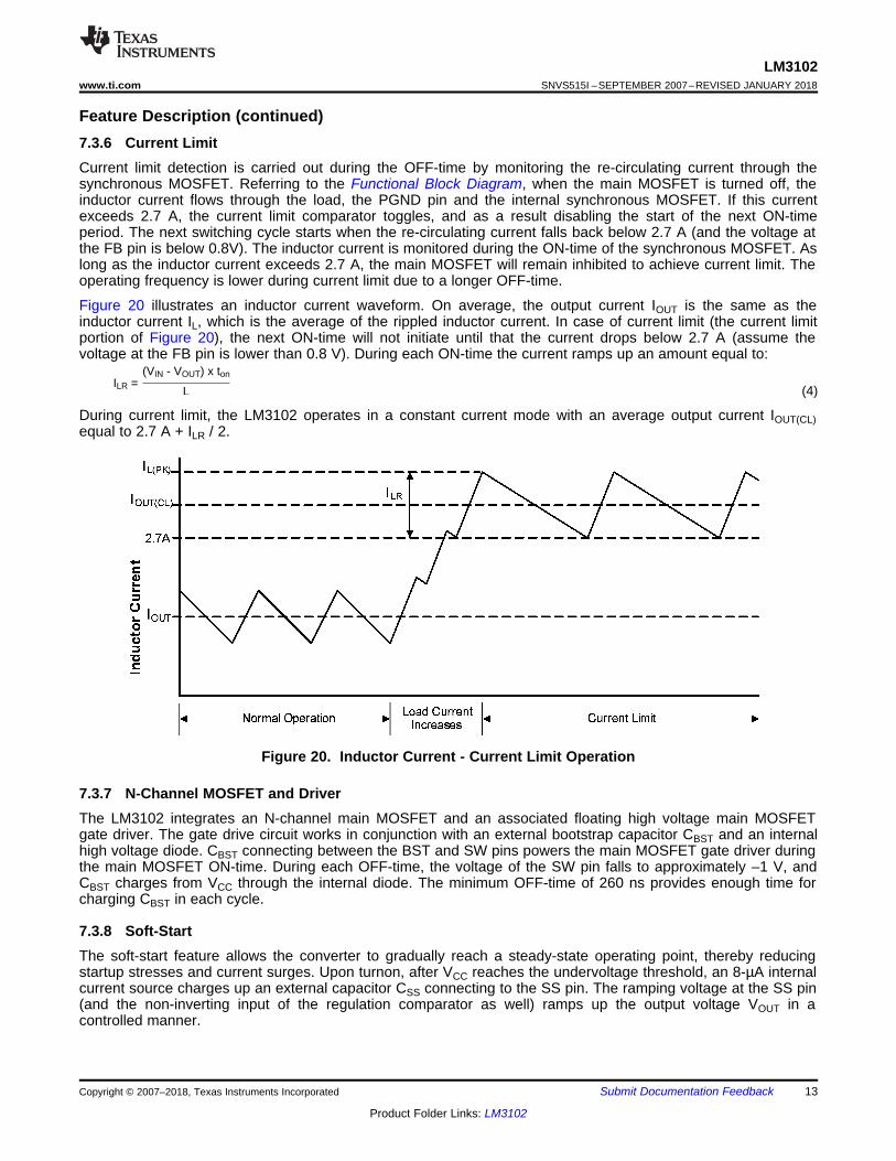
Feature Description (continued)An internal switch grounds the SS pin if any of the following three cases happens: (i) VCC is below the UVLOthreshold; (ii) a thermal shutdown occurs; or (iii) the EN pin is grounded. Alternatively, the output voltage can beshut off by connecting the SS pin to ground using an external switch. Releasing the switch allows the SS pin toramp up and the output voltage to return to normal. The shutdown configuration is shown in Figure 21.
Figure 21. Alternate Shutdown Implementation
7.3.9 Thermal ProtectionThe junction temperature of the LM3102 should not exceed the maximum limit. Thermal protection isimplemented by an internal Thermal Shutdown circuit, which activates (typically) at 165°C to make the controllerenter a low power reset state by disabling the main MOSFET, disabling the ON-timer, and grounding the SS pin.Thermal protection helps prevent catastrophic failures from accidental device overheating. When the junctiontemperature falls back below 145°C (typical hysteresis = 20°C), the SS pin is released and normal operationresumes.
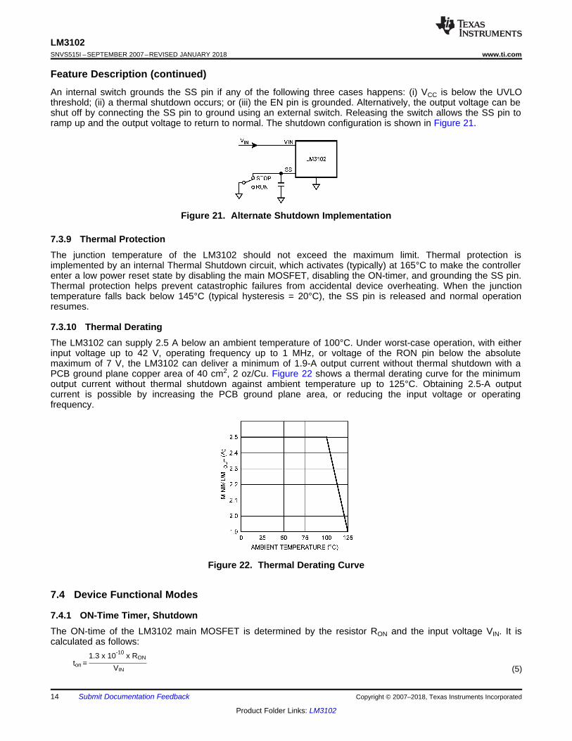
7.3.10 Thermal DeratingThe LM3102 can supply 2.5 A below an ambient temperature of 100°C. Under worst-case operation, with eitherinput voltage up to 42 V, operating frequency up to 1 MHz, or voltage of the RON pin below the absolutemaximum of 7 V, the LM3102 can deliver a minimum of 1.9-A output current without thermal shutdown with aPCB ground plane copper area of 40 cm2, 2 oz/Cu. Figure 22 shows a thermal derating curve for the minimumoutput current without thermal shutdown against ambient temperature up to 125°C. Obtaining 2.5-A outputcurrent is possible by increasing the PCB ground plane area, or reducing the input voltage or operatingfrequency.
Figure 22. Thermal Derating Curve
7.4 Device Functional Modes
7.4.1 ON-Time Timer, ShutdownThe ON-time of the LM3102 main MOSFET is determined by the resistor RON and the input voltage VIN. It iscalculated as follows:
(5)
fSW(MAX) =VOUT
VIN(MAX) x 150 ns
15
LM3102www.ti.com SNVS515I –SEPTEMBER 2007–REVISED JANUARY 2018
Product Folder Links: LM3102
Submit Documentation FeedbackCopyright © 2007–2018, Texas Instruments Incorporated
Device Functional Modes (continued)The inverse relationship of ton and VIN gives a nearly constant frequency as VIN is varied. RON should be selectedsuch that the ON-time at maximum VIN is greater than 150 ns. The ON-timer has a limiter to ensure a minimumof 150 ns for ton. This limits the maximum operating frequency, which is governed by Equation 6:
(6)
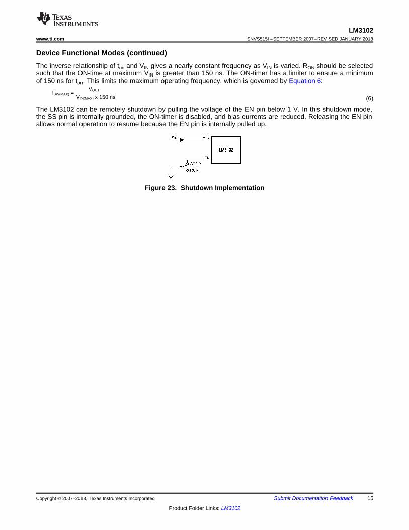
The LM3102 can be remotely shutdown by pulling the voltage of the EN pin below 1 V. In this shutdown mode,the SS pin is internally grounded, the ON-timer is disabled, and bias currents are reduced. Releasing the EN pinallows normal operation to resume because the EN pin is internally pulled up.
Figure 23. Shutdown Implementation
16
LM3102SNVS515I –SEPTEMBER 2007–REVISED JANUARY 2018 www.ti.com
Product Folder Links: LM3102
Submit Documentation Feedback Copyright © 2007–2018, Texas Instruments Incorporated
8 Application and Implementation
NOTEInformation in the following applications sections is not part of the TI componentspecification, and TI does not warrant its accuracy or completeness. TI’s customers areresponsible for determining suitability of components for their purposes. Customers shouldvalidate and test their design implementation to confirm system functionality.
8.1 Application InformationThe LM3102 is a step-down DC-to-DC controller. It is typically used to convert a higher DC voltage to a lower DCvoltage with a maximum output current of 2.5 A. The following design procedure can be used to selectcomponents for the LM3102. Alternately, the WEBENCH software may be used to generate complete designs.
When generating a design, the WEBENCH® software uses iterative design procedure and accessescomprehensive databases of components. For more details, go to www.ti.com.
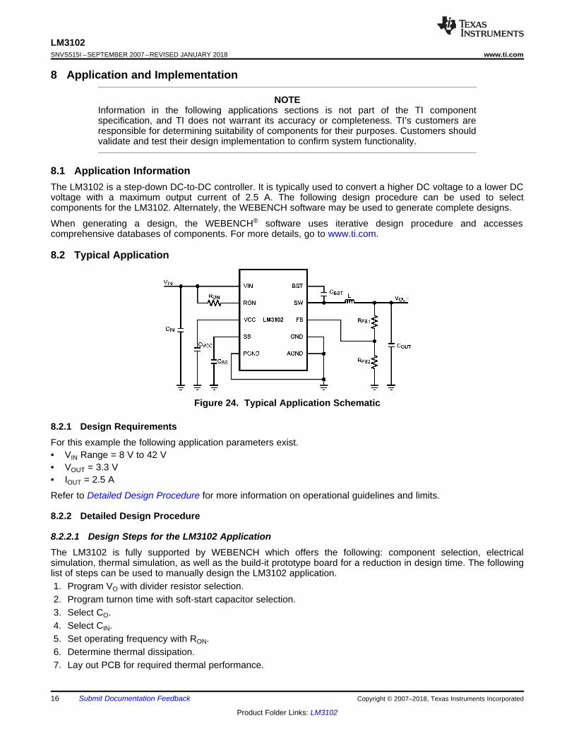
8.2 Typical Application
Figure 24. Typical Application Schematic
8.2.1 Design RequirementsFor this example the following application parameters exist.• VIN Range = 8 V to 42 V• VOUT = 3.3 V• IOUT = 2.5 A
Refer to Detailed Design Procedure for more information on operational guidelines and limits.
8.2.2 Detailed Design Procedure
8.2.2.1 Design Steps for the LM3102 ApplicationThe LM3102 is fully supported by WEBENCH which offers the following: component selection, electricalsimulation, thermal simulation, as well as the build-it prototype board for a reduction in design time. The followinglist of steps can be used to manually design the LM3102 application.1. Program VO with divider resistor selection.2. Program turnon time with soft-start capacitor selection.3. Select CO.4. Select CIN.5. Set operating frequency with RON.6. Determine thermal dissipation.7. Lay out PCB for required thermal performance.
L =ILR x fSW x VIN
VOUT x (VIN - VOUT)
1.3 x 10⁻¹⁰
VIN(MAX) x 150 nsRON t
17
LM3102www.ti.com SNVS515I –SEPTEMBER 2007–REVISED JANUARY 2018
Product Folder Links: LM3102
Submit Documentation FeedbackCopyright © 2007–2018, Texas Instruments Incorporated
Typical Application (continued)8.2.2.2 External ComponentsThe following guidelines can be used to select external components.
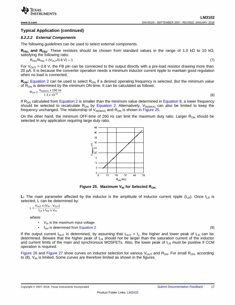
RFB1 and RFB2: These resistors should be chosen from standard values in the range of 1.0 kΩ to 10 kΩ,satisfying the following ratio:
RFB1/RFB2 = (VOUT/0.8 V) – 1 (7)
For VOUT = 0.8 V, the FB pin can be connected to the output directly with a pre-load resistor drawing more than20 µA. It is because the converter operation needs a minimum inductor current ripple to maintain good regulationwhen no load is connected.
RON: Equation 2 can be used to select RON if a desired operating frequency is selected. But the minimum valueof RON is determined by the minimum ON-time. It can be calculated as follows:
(8)
If RON calculated from Equation 2 is smaller than the minimum value determined in Equation 8, a lower frequencyshould be selected to recalculate RON by Equation 2. Alternatively, VIN(MAX) can also be limited to keep thefrequency unchanged. The relationship of VIN(MAX) and RON is shown in Figure 25.
On the other hand, the minimum OFF-time of 260 ns can limit the maximum duty ratio. Larger RON should beselected in any application requiring large duty ratio.
Figure 25. Maximum VIN for Selected RON
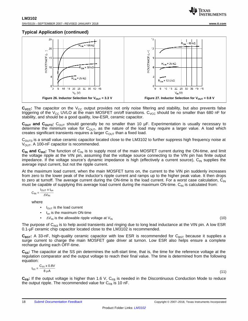
L: The main parameter affected by the inductor is the amplitude of inductor current ripple (ILR). Once ILR isselected, L can be determined by:
where• VIN is the maximum input voltage• fSW is determined from Equation 2 (9)
If the output current IOUT is determined, by assuming that IOUT = IL, the higher and lower peak of ILR can bedetermined. Beware that the higher peak of ILR should not be larger than the saturation current of the inductorand current limits of the main and synchronous MOSFETs. Also, the lower peak of ILR must be positive if CCMoperation is required.
Figure 26 and Figure 27 show curves on inductor selection for various VOUT and RON. For small RON, accordingto (8), VIN is limited. Some curves are therefore limited as shown in the figures.
tSS =8 PA
CSS x 0.8V
CIN ='VIN
IOUT x ton
18
LM3102SNVS515I –SEPTEMBER 2007–REVISED JANUARY 2018 www.ti.com
Product Folder Links: LM3102
Submit Documentation Feedback Copyright © 2007–2018, Texas Instruments Incorporated
Typical Application (continued)
Figure 26. Inductor Selection for VOUT = 3.3 V Figure 27. Inductor Selection for VOUT = 0.8 V
CVCC: The capacitor on the VCC output provides not only noise filtering and stability, but also prevents falsetriggering of the VCC UVLO at the main MOSFET on/off transitions. CVCC should be no smaller than 680 nF forstability, and should be a good quality, low-ESR, ceramic capacitor.
COUT and COUT3: COUT should generally be no smaller than 10 µF. Experimentation is usually necessary todetermine the minimum value for COUT, as the nature of the load may require a larger value. A load whichcreates significant transients requires a larger COUT than a fixed load.
COUT3 is a small value ceramic capacitor located close to the LM3102 to further suppress high frequency noise atVOUT. A 100-nF capacitor is recommended.
CIN and CIN3: The function of CIN is to supply most of the main MOSFET current during the ON-time, and limitthe voltage ripple at the VIN pin, assuming that the voltage source connecting to the VIN pin has finite outputimpedance. If the voltage source’s dynamic impedance is high (effectively a current source), CIN supplies theaverage input current, but not the ripple current.
At the maximum load current, when the main MOSFET turns on, the current to the VIN pin suddenly increasesfrom zero to the lower peak of the inductor’s ripple current and ramps up to the higher peak value. It then dropsto zero at turnoff. The average current during the ON-time is the load current. For a worst case calculation, CINmust be capable of supplying this average load current during the maximum ON-time. CIN is calculated from:
where• IOUT is the load current• ton is the maximum ON-time• ΔVIN is the allowable ripple voltage at VIN (10)
The purpose of CIN3 is to help avoid transients and ringing due to long lead inductance at the VIN pin. A low ESR0.1-µF ceramic chip capacitor located close to the LM3102 is recommended.
CBST: A 33-nF, high-quality ceramic capacitor with low ESR is recommended for CBST because it supplies asurge current to charge the main MOSFET gate driver at turnon. Low ESR also helps ensure a completerecharge during each OFF-time.
CSS: The capacitor at the SS pin determines the soft-start time, that is, the time for the reference voltage at theregulation comparator and the output voltage to reach their final value. The time is determined from the followingequation:
(11)
CFB: If the output voltage is higher than 1.6 V, CFB is needed in the Discontinuous Conduction Mode to reducethe output ripple. The recommended value for CFB is 10 nF.
19
LM3102www.ti.com SNVS515I –SEPTEMBER 2007–REVISED JANUARY 2018
Product Folder Links: LM3102
Submit Documentation FeedbackCopyright © 2007–2018, Texas Instruments Incorporated
Typical Application (continued)8.2.3 Application Curve
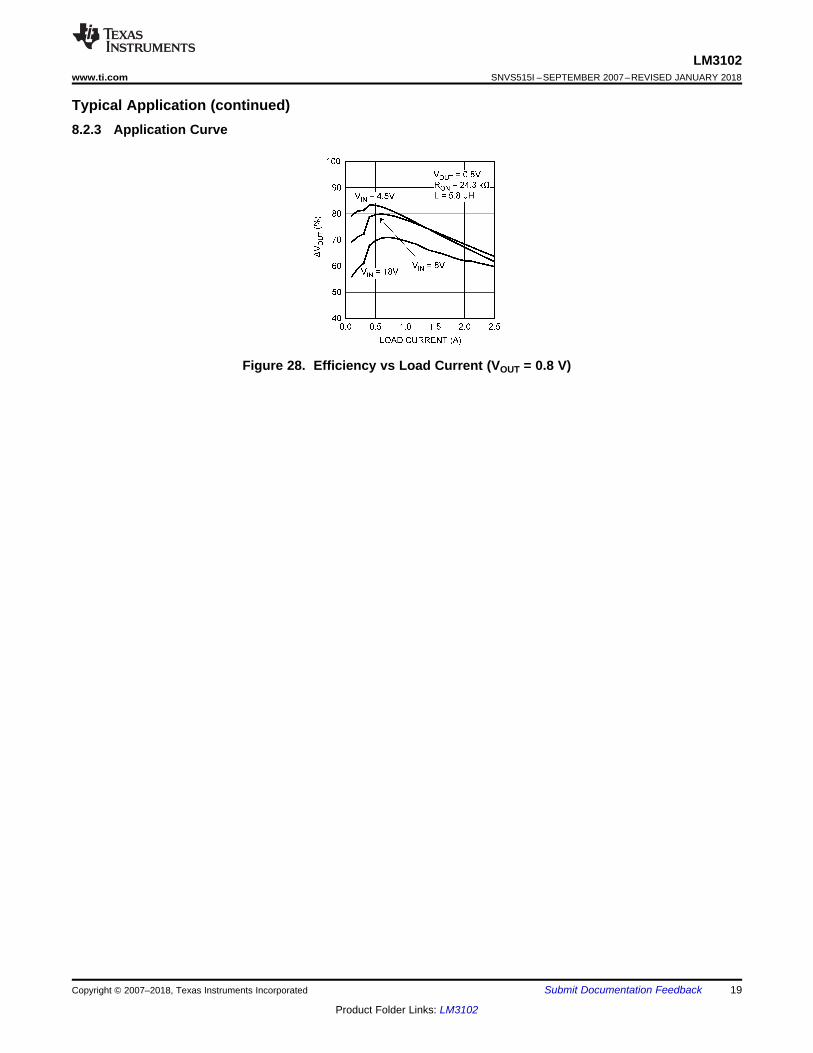
Figure 28. Efficiency vs Load Current (VOUT = 0.8 V)
20
LM3102SNVS515I –SEPTEMBER 2007–REVISED JANUARY 2018 www.ti.com
Product Folder Links: LM3102
Submit Documentation Feedback Copyright © 2007–2018, Texas Instruments Incorporated
8.3 System Examples
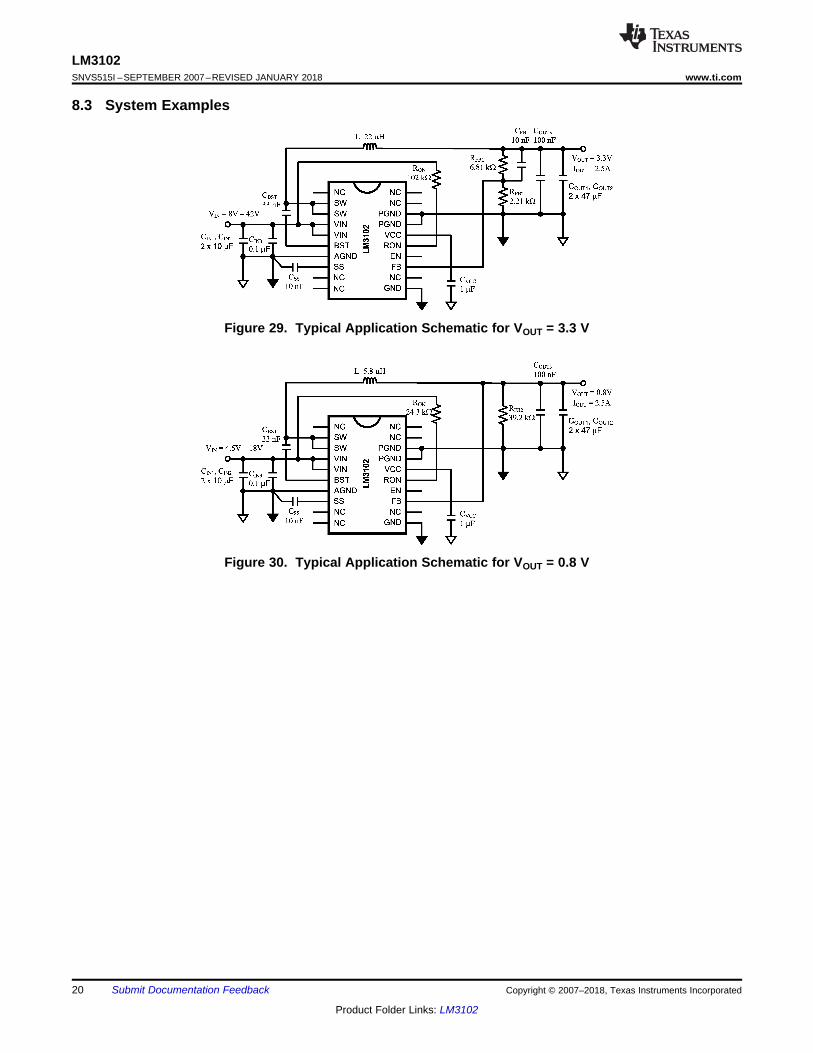
Figure 29. Typical Application Schematic for VOUT = 3.3 V
Figure 30. Typical Application Schematic for VOUT = 0.8 V
+-
L
COUTCIN LOADVSUPPLY
21
LM3102www.ti.com SNVS515I –SEPTEMBER 2007–REVISED JANUARY 2018
Product Folder Links: LM3102
Submit Documentation FeedbackCopyright © 2007–2018, Texas Instruments Incorporated
9 Power Supply RecommendationsThe LM3102 device is designed to operate from an input voltage supply range between 4.5 V and 42 V. Thisinput supply should be well regulated and able to withstand maximum input current and maintain a stablevoltage. The resistance of the input supply rail should be low enough that an input current transient does notcause a high enough drop at the LM3102 supply voltage that can cause a false UVLO fault triggering and systemreset. If the input supply is more than a few inches from the LM3102, additional bulk capacitance may berequired in addition to the ceramic bypass capacitors. The amount of bulk capacitance is not critical, but a 47-μFor 100-μF electrolytic capacitor is a typical choice.
10 Layout
10.1 Layout GuidelinesThe LM3102 regulation, overvoltage, and current limit comparators are very fast so they will respond to shortduration noise pulses. Layout is therefore critical for optimum performance. It must be as neat and compact aspossible, and all external components must be as close to their associated pins of the LM3102 as possible.
Refer to Layout Example, the loop formed by CIN, the main and synchronous MOSFET internal to the LM3102,and the PGND pin should be as small as possible. The connection from the PGND pin to CIN should be as shortand direct as possible. Vias should be added to connect the ground of CIN to a ground plane, located as close tothe capacitor as possible. The bootstrap capacitor CBST should be connected as close to the SW and BST pinsas possible, and the connecting traces should be thick. The feedback resistors and capacitor RFB1, RFB2, and CFBshould be close to the FB pin.
A long trace running from VOUT to RFB1 is generally acceptable because this is a low-impedance node. GroundRFB2 directly to the AGND pin (pin 7). The output capacitor COUT should be connected close to the load and tieddirectly to the ground plane. The inductor L should be connected close to the SW pin with as short a trace aspossible to reduce the potential for EMI (electromagnetic interference) generation.
If it is expected that the internal dissipation of the LM3102 will produce excessive junction temperature duringnormal operation, making good use of the PCB ground plane can help considerably to dissipate heat. Theexposed pad on the bottom of the LM3102 IC package can be soldered to the ground plane, which shouldextend out from beneath the LM3102 to help dissipate heat.
The exposed pad is internally connected to the LM3102 IC substrate. Additionally the use of thick traces, wherepossible, can help conduct heat away from the LM3102. Using numerous vias to connect the die attached pad tothe ground plane is a good practice. Judicious positioning of the PCB within the end product, along with the useof any available air flow (forced or natural convection) can help reduce the junction temperature.
10.2 Layout Example
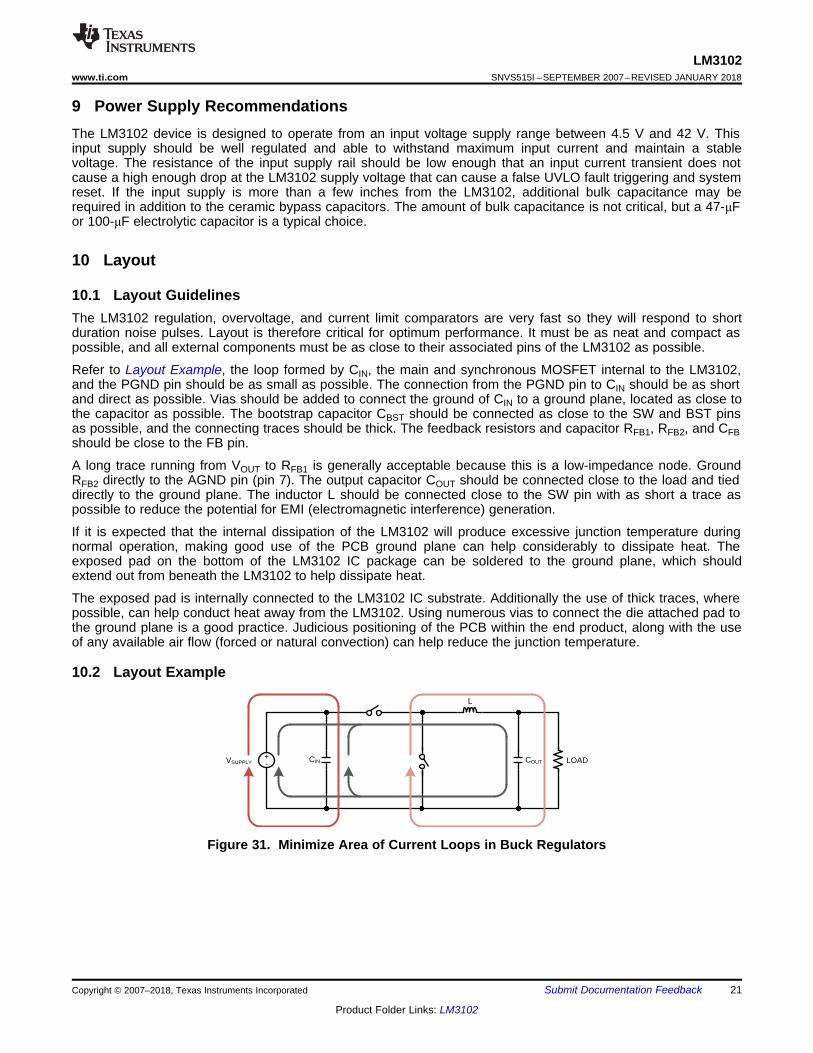
Figure 31. Minimize Area of Current Loops in Buck Regulators

NC
PGND
NC
SW
VIN
VIN
BST
AGND
SS
VCC
RON
EN
FB
SW NC
PGND
PAD (21)
1 20
2
3
4
5
6
8 13
19
18
17
16
15
14
Thermal Vias under DAP
NC
NC 10
9 NC
GND
12
11
CBOOT RON
PGND
L
RFBT
CFF
VOUT sense point is away from inductor and
past COUT
VOUT distribution point is away from inductor and past COUT
TO LOAD
Route VOUT sense trace away from SW and VIN nodes. Preferably shielded in an alternative layer
GND Plane
Add as much copper area as possible to enhance overall thermal performance
VIN
CIN
RFBB
Connect RON to VIN
COUT
VOUT
GND
SW
CVCC
CSS
7Refer Data sheet
for EN options
22
LM3102SNVS515I –SEPTEMBER 2007–REVISED JANUARY 2018 www.ti.com
Product Folder Links: LM3102
Submit Documentation Feedback Copyright © 2007–2018, Texas Instruments Incorporated
Layout Example (continued)
Figure 32. PCB Layout Example - Top View
23
LM3102www.ti.com SNVS515I –SEPTEMBER 2007–REVISED JANUARY 2018
Product Folder Links: LM3102
Submit Documentation FeedbackCopyright © 2007–2018, Texas Instruments Incorporated
11 Device and Documentation Support
11.1 Community ResourcesThe following links connect to TI community resources. Linked contents are provided "AS IS" by the respectivecontributors. They do not constitute TI specifications and do not necessarily reflect TI's views; see TI's Terms ofUse.
TI E2E™ Online Community TI's Engineer-to-Engineer (E2E) Community. Created to foster collaborationamong engineers. At e2e.ti.com, you can ask questions, share knowledge, explore ideas and helpsolve problems with fellow engineers.
Design Support TI's Design Support Quickly find helpful E2E forums along with design support tools andcontact information for technical support.
11.2 TrademarksE2E is a trademark of Texas Instruments.WEBENCH is a registered trademark of Texas Instruments.All other trademarks are the property of their respective owners.
11.3 Electrostatic Discharge CautionThese devices have limited built-in ESD protection. The leads should be shorted together or the device placed in conductive foamduring storage or handling to prevent electrostatic damage to the MOS gates.
11.4 GlossarySLYZ022 — TI Glossary.
This glossary lists and explains terms, acronyms, and definitions.
12 Mechanical, Packaging, and Orderable InformationThe following pages include mechanical, packaging, and orderable information. This information is the mostcurrent data available for the designated devices. This data is subject to change without notice and revision ofthis document. For browser-based versions of this data sheet, refer to the left-hand navigation.
PACKAGE OPTION ADDENDUM
www.ti.com 13-Oct-2017
Addendum-Page 1
PACKAGING INFORMATION
Orderable Device Status(1)
Package Type PackageDrawing
Pins PackageQty
Eco Plan(2)
Lead/Ball Finish(6)
MSL Peak Temp(3)
Op Temp (°C) Device Marking(4/5)
Samples
LM3102MH/NOPB ACTIVE HTSSOP PWP 20 73 Green (RoHS& no Sb/Br)
CU SN Level-1-260C-UNLIM -40 to 125 LM3102MH
LM3102MHX/NOPB ACTIVE HTSSOP PWP 20 2500 Green (RoHS& no Sb/Br)
CU SN Level-1-260C-UNLIM -40 to 125 LM3102MH
LM3102QMH/NOPB ACTIVE HTSSOP PWP 20 73 Green (RoHS& no Sb/Br)
CU SN Level-1-260C-UNLIM -40 to 125 LM3102QMH
LM3102QMHX/NOPB ACTIVE HTSSOP PWP 20 2500 Green (RoHS& no Sb/Br)
CU SN Level-1-260C-UNLIM -40 to 125 LM3102QMH
LM3102TL-1/NOPB ACTIVE DSBGA YPA 28 250 Green (RoHS& no Sb/Br)
SNAGCU Level-1-260C-UNLIM 3102
LM3102TLX-1/NOPB ACTIVE DSBGA YPA 28 1000 Green (RoHS& no Sb/Br)
SNAGCU Level-1-260C-UNLIM 3102
(1) The marketing status values are defined as follows:ACTIVE: Product device recommended for new designs.LIFEBUY: TI has announced that the device will be discontinued, and a lifetime-buy period is in effect.NRND: Not recommended for new designs. Device is in production to support existing customers, but TI does not recommend using this part in a new design.PREVIEW: Device has been announced but is not in production. Samples may or may not be available.OBSOLETE: TI has discontinued the production of the device.
(2) RoHS: TI defines "RoHS" to mean semiconductor products that are compliant with the current EU RoHS requirements for all 10 RoHS substances, including the requirement that RoHS substancedo not exceed 0.1% by weight in homogeneous materials. Where designed to be soldered at high temperatures, "RoHS" products are suitable for use in specified lead-free processes. TI mayreference these types of products as "Pb-Free".RoHS Exempt: TI defines "RoHS Exempt" to mean products that contain lead but are compliant with EU RoHS pursuant to a specific EU RoHS exemption.Green: TI defines "Green" to mean the content of Chlorine (Cl) and Bromine (Br) based flame retardants meet JS709B low halogen requirements of <=1000ppm threshold. Antimony trioxide basedflame retardants must also meet the <=1000ppm threshold requirement.
(3) MSL, Peak Temp. - The Moisture Sensitivity Level rating according to the JEDEC industry standard classifications, and peak solder temperature.
(4) There may be additional marking, which relates to the logo, the lot trace code information, or the environmental category on the device.
(5) Multiple Device Markings will be inside parentheses. Only one Device Marking contained in parentheses and separated by a "~" will appear on a device. If a line is indented then it is a continuationof the previous line and the two combined represent the entire Device Marking for that device.
PACKAGE OPTION ADDENDUM
www.ti.com 13-Oct-2017
Addendum-Page 2
(6) Lead/Ball Finish - Orderable Devices may have multiple material finish options. Finish options are separated by a vertical ruled line. Lead/Ball Finish values may wrap to two lines if the finishvalue exceeds the maximum column width.
Important Information and Disclaimer:The information provided on this page represents TI's knowledge and belief as of the date that it is provided. TI bases its knowledge and belief on informationprovided by third parties, and makes no representation or warranty as to the accuracy of such information. Efforts are underway to better integrate information from third parties. TI has taken andcontinues to take reasonable steps to provide representative and accurate information but may not have conducted destructive testing or chemical analysis on incoming materials and chemicals.TI and TI suppliers consider certain information to be proprietary, and thus CAS numbers and other limited information may not be available for release.
In no event shall TI's liability arising out of such information exceed the total purchase price of the TI part(s) at issue in this document sold by TI to Customer on an annual basis.
OTHER QUALIFIED VERSIONS OF LM3102, LM3102-Q1 :
• Catalog: LM3102
• Automotive: LM3102-Q1
NOTE: Qualified Version Definitions:
• Catalog - TI's standard catalog product
• Automotive - Q100 devices qualified for high-reliability automotive applications targeting zero defects
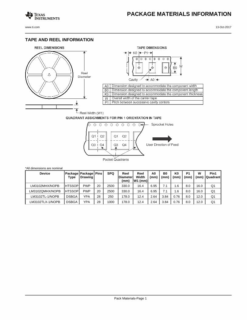
TAPE AND REEL INFORMATION
*All dimensions are nominal
Device PackageType
PackageDrawing
Pins SPQ ReelDiameter
(mm)
ReelWidth
W1 (mm)
A0(mm)
B0(mm)
K0(mm)
P1(mm)
W(mm)
Pin1Quadrant
LM3102MHX/NOPB HTSSOP PWP 20 2500 330.0 16.4 6.95 7.1 1.6 8.0 16.0 Q1
LM3102QMHX/NOPB HTSSOP PWP 20 2500 330.0 16.4 6.95 7.1 1.6 8.0 16.0 Q1
LM3102TL-1/NOPB DSBGA YPA 28 250 178.0 12.4 2.64 3.84 0.76 8.0 12.0 Q1
LM3102TLX-1/NOPB DSBGA YPA 28 1000 178.0 12.4 2.64 3.84 0.76 8.0 12.0 Q1
PACKAGE MATERIALS INFORMATION
www.ti.com 13-Oct-2017
Pack Materials-Page 1
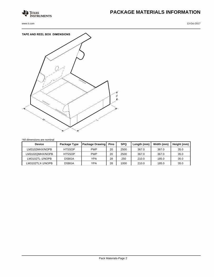
*All dimensions are nominal
Device Package Type Package Drawing Pins SPQ Length (mm) Width (mm) Height (mm)
LM3102MHX/NOPB HTSSOP PWP 20 2500 367.0 367.0 35.0
LM3102QMHX/NOPB HTSSOP PWP 20 2500 367.0 367.0 35.0
LM3102TL-1/NOPB DSBGA YPA 28 250 210.0 185.0 35.0
LM3102TLX-1/NOPB DSBGA YPA 28 1000 210.0 185.0 35.0
PACKAGE MATERIALS INFORMATION
www.ti.com 13-Oct-2017
Pack Materials-Page 2
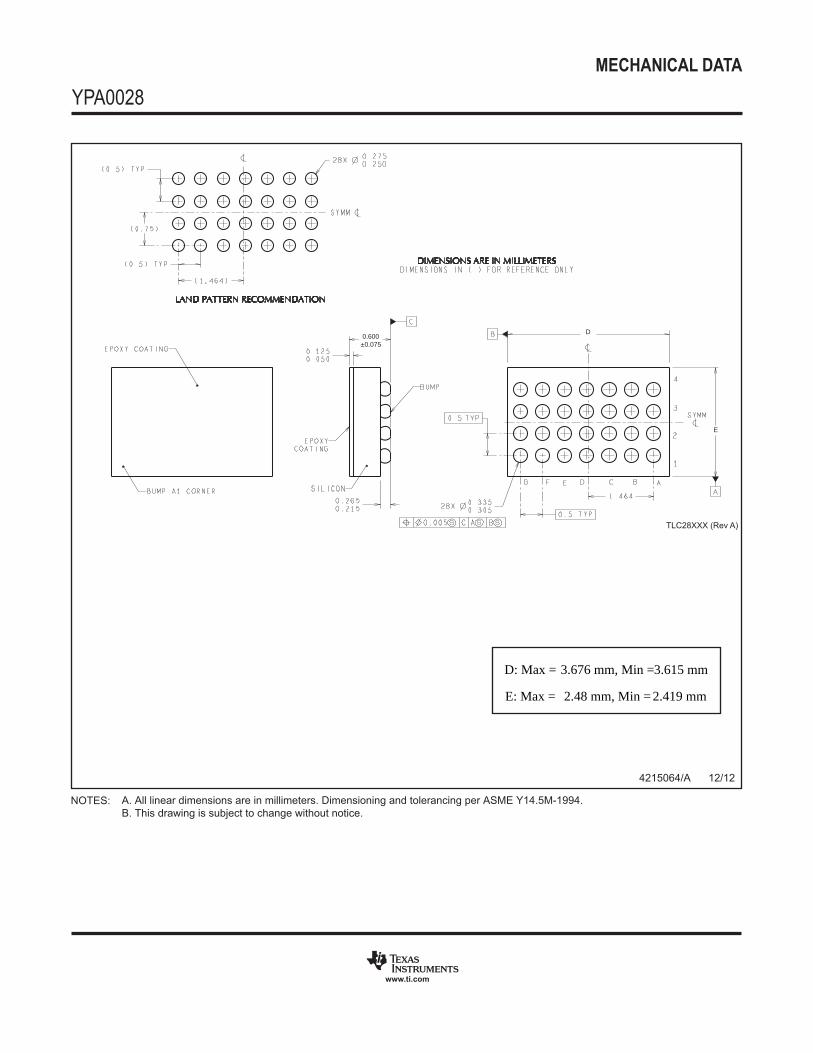
MECHANICAL DATA
YPA0028
www.ti.com
TLC28XXX (Rev A)
A. All linear dimensions are in millimeters. Dimensioning and tolerancing per ASME Y14.5M-1994. B. This drawing is subject to change without notice.
4215064/A 12/12
NOTES:
0.600±0.075
E
D
D: Max =
E: Max =
3.676 mm, Min =
2.48 mm, Min =
3.615 mm
2.419 mm
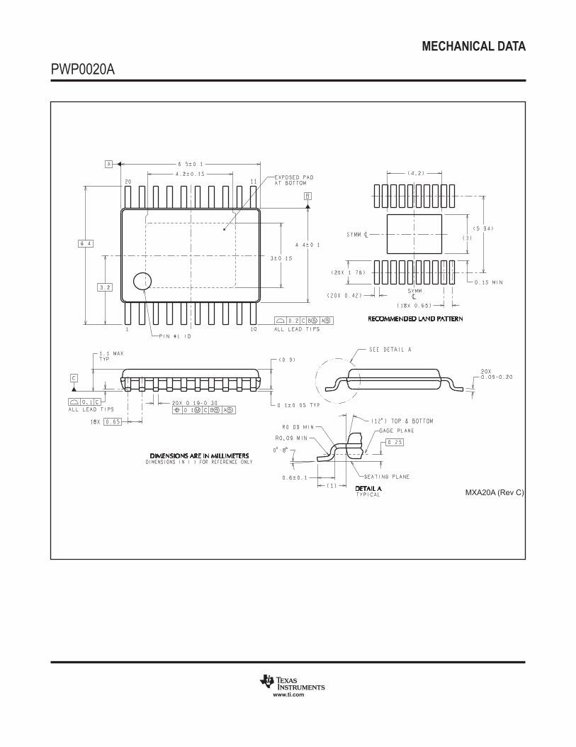
MECHANICAL DATA
PWP0020A
www.ti.com
MXA20A (Rev C)
IMPORTANT NOTICE
Texas Instruments Incorporated (TI) reserves the right to make corrections, enhancements, improvements and other changes to itssemiconductor products and services per JESD46, latest issue, and to discontinue any product or service per JESD48, latest issue. Buyersshould obtain the latest relevant information before placing orders and should verify that such information is current and complete.TI’s published terms of sale for semiconductor products (http://www.ti.com/sc/docs/stdterms.htm) apply to the sale of packaged integratedcircuit products that TI has qualified and released to market. Additional terms may apply to the use or sale of other types of TI products andservices.Reproduction of significant portions of TI information in TI data sheets is permissible only if reproduction is without alteration and isaccompanied by all associated warranties, conditions, limitations, and notices. TI is not responsible or liable for such reproduceddocumentation. Information of third parties may be subject to additional restrictions. Resale of TI products or services with statementsdifferent from or beyond the parameters stated by TI for that product or service voids all express and any implied warranties for theassociated TI product or service and is an unfair and deceptive business practice. TI is not responsible or liable for any such statements.Buyers and others who are developing systems that incorporate TI products (collectively, “Designers”) understand and agree that Designersremain responsible for using their independent analysis, evaluation and judgment in designing their applications and that Designers havefull and exclusive responsibility to assure the safety of Designers' applications and compliance of their applications (and of all TI productsused in or for Designers’ applications) with all applicable regulations, laws and other applicable requirements. Designer represents that, withrespect to their applications, Designer has all the necessary expertise to create and implement safeguards that (1) anticipate dangerousconsequences of failures, (2) monitor failures and their consequences, and (3) lessen the likelihood of failures that might cause harm andtake appropriate actions. Designer agrees that prior to using or distributing any applications that include TI products, Designer willthoroughly test such applications and the functionality of such TI products as used in such applications.TI’s provision of technical, application or other design advice, quality characterization, reliability data or other services or information,including, but not limited to, reference designs and materials relating to evaluation modules, (collectively, “TI Resources”) are intended toassist designers who are developing applications that incorporate TI products; by downloading, accessing or using TI Resources in anyway, Designer (individually or, if Designer is acting on behalf of a company, Designer’s company) agrees to use any particular TI Resourcesolely for this purpose and subject to the terms of this Notice.TI’s provision of TI Resources does not expand or otherwise alter TI’s applicable published warranties or warranty disclaimers for TIproducts, and no additional obligations or liabilities arise from TI providing such TI Resources. TI reserves the right to make corrections,enhancements, improvements and other changes to its TI Resources. TI has not conducted any testing other than that specificallydescribed in the published documentation for a particular TI Resource.Designer is authorized to use, copy and modify any individual TI Resource only in connection with the development of applications thatinclude the TI product(s) identified in such TI Resource. NO OTHER LICENSE, EXPRESS OR IMPLIED, BY ESTOPPEL OR OTHERWISETO ANY OTHER TI INTELLECTUAL PROPERTY RIGHT, AND NO LICENSE TO ANY TECHNOLOGY OR INTELLECTUAL PROPERTYRIGHT OF TI OR ANY THIRD PARTY IS GRANTED HEREIN, including but not limited to any patent right, copyright, mask work right, orother intellectual property right relating to any combination, machine, or process in which TI products or services are used. Informationregarding or referencing third-party products or services does not constitute a license to use such products or services, or a warranty orendorsement thereof. Use of TI Resources may require a license from a third party under the patents or other intellectual property of thethird party, or a license from TI under the patents or other intellectual property of TI.TI RESOURCES ARE PROVIDED “AS IS” AND WITH ALL FAULTS. TI DISCLAIMS ALL OTHER WARRANTIES ORREPRESENTATIONS, EXPRESS OR IMPLIED, REGARDING RESOURCES OR USE THEREOF, INCLUDING BUT NOT LIMITED TOACCURACY OR COMPLETENESS, TITLE, ANY EPIDEMIC FAILURE WARRANTY AND ANY IMPLIED WARRANTIES OFMERCHANTABILITY, FITNESS FOR A PARTICULAR PURPOSE, AND NON-INFRINGEMENT OF ANY THIRD PARTY INTELLECTUALPROPERTY RIGHTS. TI SHALL NOT BE LIABLE FOR AND SHALL NOT DEFEND OR INDEMNIFY DESIGNER AGAINST ANY CLAIM,INCLUDING BUT NOT LIMITED TO ANY INFRINGEMENT CLAIM THAT RELATES TO OR IS BASED ON ANY COMBINATION OFPRODUCTS EVEN IF DESCRIBED IN TI RESOURCES OR OTHERWISE. IN NO EVENT SHALL TI BE LIABLE FOR ANY ACTUAL,DIRECT, SPECIAL, COLLATERAL, INDIRECT, PUNITIVE, INCIDENTAL, CONSEQUENTIAL OR EXEMPLARY DAMAGES INCONNECTION WITH OR ARISING OUT OF TI RESOURCES OR USE THEREOF, AND REGARDLESS OF WHETHER TI HAS BEENADVISED OF THE POSSIBILITY OF SUCH DAMAGES.Unless TI has explicitly designated an individual product as meeting the requirements of a particular industry standard (e.g., ISO/TS 16949and ISO 26262), TI is not responsible for any failure to meet such industry standard requirements.Where TI specifically promotes products as facilitating functional safety or as compliant with industry functional safety standards, suchproducts are intended to help enable customers to design and create their own applications that meet applicable functional safety standardsand requirements. Using products in an application does not by itself establish any safety features in the application. Designers mustensure compliance with safety-related requirements and standards applicable to their applications. Designer may not use any TI products inlife-critical medical equipment unless authorized officers of the parties have executed a special contract specifically governing such use.Life-critical medical equipment is medical equipment where failure of such equipment would cause serious bodily injury or death (e.g., lifesupport, pacemakers, defibrillators, heart pumps, neurostimulators, and implantables). Such equipment includes, without limitation, allmedical devices identified by the U.S. Food and Drug Administration as Class III devices and equivalent classifications outside the U.S.TI may expressly designate certain products as completing a particular qualification (e.g., Q100, Military Grade, or Enhanced Product).Designers agree that it has the necessary expertise to select the product with the appropriate qualification designation for their applicationsand that proper product selection is at Designers’ own risk. Designers are solely responsible for compliance with all legal and regulatoryrequirements in connection with such selection.Designer will fully indemnify TI and its representatives against any damages, costs, losses, and/or liabilities arising out of Designer’s non-compliance with the terms and provisions of this Notice.
Mailing Address: Texas Instruments, Post Office Box 655303, Dallas, Texas 75265Copyright © 2018, Texas Instruments Incorporated