Embed Size (px)
Citation preview
LM723, LM723C
www.ti.com SNVS765C –JUNE 1999–REVISED APRIL 2013
LM723/LM723C Voltage RegulatorCheck for Samples: LM723, LM723C
1FEATURES DESCRIPTIONThe LM723/LM723C is a voltage regulator designed
2• 150 mA Output Current Without External Passprimarily for series regulator applications. By itself, itTransistorwill supply output currents up to 150 mA; but external
• Output Currents in Excess of 10A Possible by transistors can be added to provide any desired loadAdding External Transistors current. The circuit features extremely low standby
current drain, and provision is made for either linear• Input Voltage 40V Maxor foldback current limiting.• Output Voltage Adjustable from 2V to 37VThe LM723/LM723C is also useful in a wide range of• Can be Used as Either a Linear or a Switchingother applications such as a shunt regulator, aRegulatorcurrent regulator or a temperature controller.
The LM723C is identical to the LM723 except that theLM723C has its performance ensured over a 0°C to+70°C temperature range, instead of −55°C to+125°C.
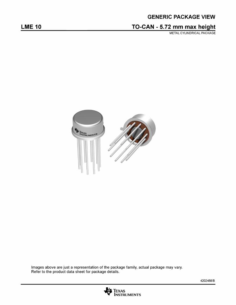
Connection Diagram
Note: Pin 5 connected to case.
Figure 1. Top View Figure 2. Top ViewCDIP Package or PDIP Package TO-100
See Package J or NFF0014A See Package LME
Figure 3. Top ViewSee Package NAJ0020A
1
Please be aware that an important notice concerning availability, standard warranty, and use in critical applications ofTexas Instruments semiconductor products and disclaimers thereto appears at the end of this data sheet.
2All trademarks are the property of their respective owners.
PRODUCTION DATA information is current as of publication date. Copyright © 1999–2013, Texas Instruments IncorporatedProducts conform to specifications per the terms of the TexasInstruments standard warranty. Production processing does notnecessarily include testing of all parameters.
LM723, LM723C
SNVS765C –JUNE 1999–REVISED APRIL 2013 www.ti.com
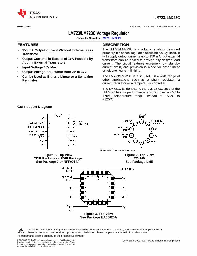
Equivalent Circuit*
*Pin numbers refer to metal can package.
Typical Application
for minimum temperature drift.
Typical Performance
Regulated Output Voltage 5V
Line Regulation (ΔVIN = 3V) 0.5mV
Load Regulation (ΔIL = 50 mA) 1.5mV
Figure 4. Basic Low Voltage Regulator (VOUT = 2 to 7 Volts)
2 Submit Documentation Feedback Copyright © 1999–2013, Texas Instruments Incorporated
Product Folder Links: LM723 LM723C
LM723, LM723C
www.ti.com SNVS765C –JUNE 1999–REVISED APRIL 2013
These devices have limited built-in ESD protection. The leads should be shorted together or the device placed in conductive foamduring storage or handling to prevent electrostatic damage to the MOS gates.
ABSOLUTE MAXIMUM RATINGS (1) (2)
Pulse Voltage from V+ to V− (50 ms) 50V
Continuous Voltage from V+ to V− 40V
Input-Output Voltage Differential 40V
Maximum Amplifier Input Voltage(Either Input) 8.5V
Maximum Amplifier Input Voltage(Differential) 5V
Current from VZ 25 mA
Current from VREF 15 mA
Internal Power DissipationMetal Can (3) 800 mW
CDIP (3) 900 mW
PDIP (3) 660 mW
Operating Temperature Range
LM723 −55°C to +150°C
LM723C 0°C to +70°C
Storage Temperature RangeMetal Can −65°C to +150°C
PDIP −55°C to +150°C
Lead Temperature (Soldering, 4 sec. max.)
Hermetic Package 300°C
Plastic Package 260°C
ESD Tolerance 1200V
(Human body model, 1.5 kΩ in series with 100 pF)
(1) “Absolute Maximum Ratings” indicate limits beyond which damage to the device may occur. Operating Ratings indicate conditions forwhich the device is functional, but do not ensure specific performance limits.
(2) A military RETS specification is available on request. At the time of printing, the LM723 RETS specification complied with the Min andMax limits in this table. The LM723E, H, and J may also be procured as a Standard Military Drawing.
(3) See derating curves for maximum power rating above 25°C.
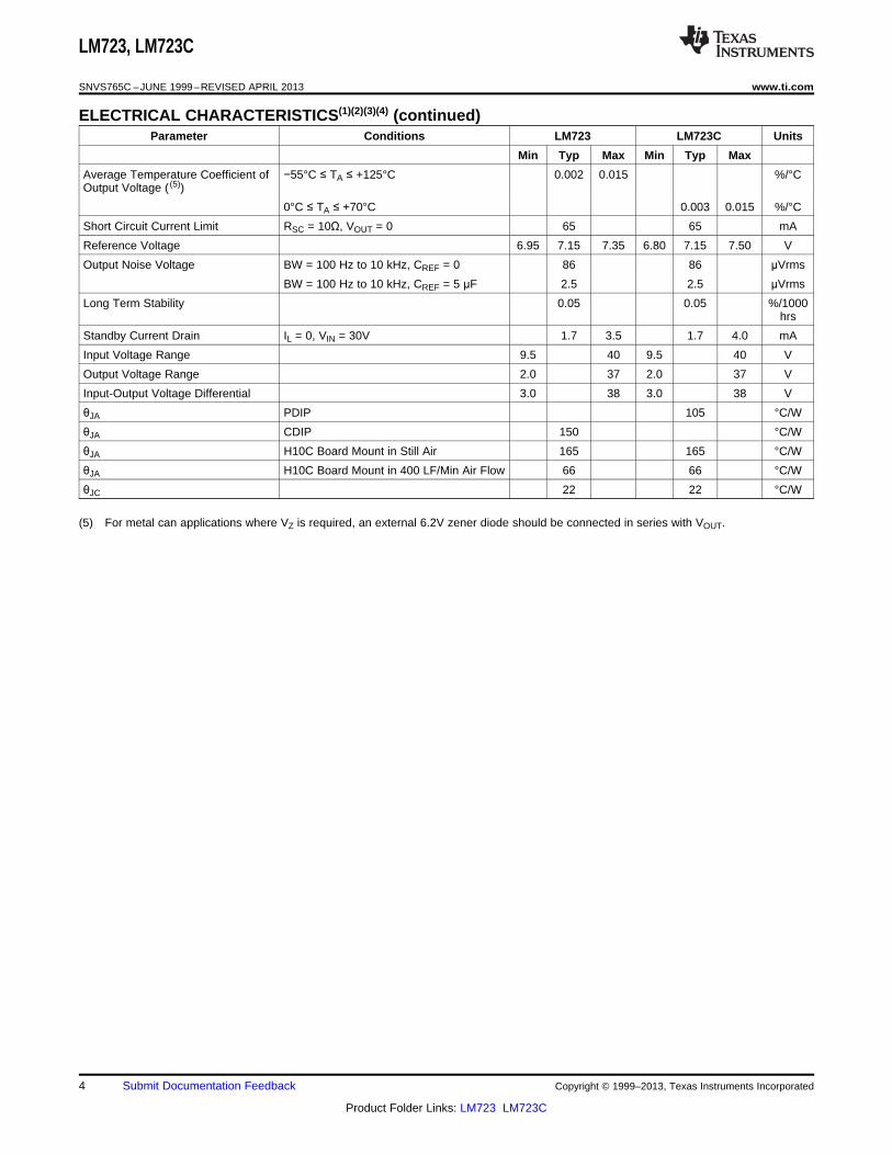
ELECTRICAL CHARACTERISTICS (1) (2) (3) (4)
Parameter Conditions LM723 LM723C Units
Min Typ Max Min Typ Max
Line Regulation VIN = 12V to VIN = 15V 0.01 0.1 0.01 0.1 % VOUT
−55°C ≤ TA ≤ +125°C 0.3 % VOUT
0°C ≤ TA ≤ +70°C 0.3 % VOUT
VIN = 12V to VIN = 40V 0.02 0.2 0.1 0.5 % VOUT
Load Regulation IL = 1 mA to IL = 50 mA 0.03 0.15 0.03 0.2 % VOUT
−55°C ≤ TA ≤ +125°C 0.6 % VOUT
0°C ≤ TA ≤ +70°C 0.6 % VOUT
Ripple Rejection f = 50 Hz to 10 kHz, CREF = 0 74 74 dB
f = 50 Hz to 10 kHz, CREF = 5 μF 86 86 dB
(1) Unless otherwise specified, TA = 25°C, VIN = V+ = VC = 12V, V− = 0, VOUT = 5V, IL = 1 mA, RSC = 0, C1 = 100 pF, CREF = 0 and dividerimpedance as seen by error amplifier ≤ 10 kΩ connected as shown in Figure 4. Line and load regulation specifications are given for thecondition of constant chip temperature. Temperature drifts must be taken into account separately for high dissipation conditions.
(2) A military RETS specification is available on request. At the time of printing, the LM723 RETS specification complied with the Min andMax limits in this table. The LM723E, H, and J may also be procured as a Standard Military Drawing.
(3) Specified by correlation to other tests.(4) L1 is 40 turns of No. 20 enameled copper wire wound on Ferroxcube P36/22-3B7 pot core or equivalent with 0.009 in. air gap.
Copyright © 1999–2013, Texas Instruments Incorporated Submit Documentation Feedback 3
Product Folder Links: LM723 LM723C
LM723, LM723C
SNVS765C –JUNE 1999–REVISED APRIL 2013 www.ti.com
ELECTRICAL CHARACTERISTICS(1)(2)(3)(4) (continued)Parameter Conditions LM723 LM723C Units
Min Typ Max Min Typ Max
Average Temperature Coefficient of −55°C ≤ TA ≤ +125°C 0.002 0.015 %/°COutput Voltage ( (5))
0°C ≤ TA ≤ +70°C 0.003 0.015 %/°C
Short Circuit Current Limit RSC = 10Ω, VOUT = 0 65 65 mA
Reference Voltage 6.95 7.15 7.35 6.80 7.15 7.50 V
Output Noise Voltage BW = 100 Hz to 10 kHz, CREF = 0 86 86 μVrms
BW = 100 Hz to 10 kHz, CREF = 5 μF 2.5 2.5 μVrms
Long Term Stability 0.05 0.05 %/1000hrs
Standby Current Drain IL = 0, VIN = 30V 1.7 3.5 1.7 4.0 mA
Input Voltage Range 9.5 40 9.5 40 V
Output Voltage Range 2.0 37 2.0 37 V
Input-Output Voltage Differential 3.0 38 3.0 38 V
θJA PDIP 105 °C/W
θJA CDIP 150 °C/W
θJA H10C Board Mount in Still Air 165 165 °C/W
θJA H10C Board Mount in 400 LF/Min Air Flow 66 66 °C/W
θJC 22 22 °C/W
(5) For metal can applications where VZ is required, an external 6.2V zener diode should be connected in series with VOUT.
4 Submit Documentation Feedback Copyright © 1999–2013, Texas Instruments Incorporated
Product Folder Links: LM723 LM723C
LM723, LM723C
www.ti.com SNVS765C –JUNE 1999–REVISED APRIL 2013
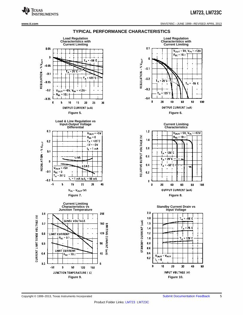
TYPICAL PERFORMANCE CHARACTERISTICS
Load Regulation Load RegulationCharacteristics with Characteristics with
Current Limiting Current Limiting
Figure 5. Figure 6.
Load & Line Regulation vsInput-Output Voltage Current Limiting
Differential Characteristics
Figure 7. Figure 8.
Current LimitingCharacteristics vs Standby Current Drain vs
Junction Temperature Input Voltage
Figure 9. Figure 10.
Copyright © 1999–2013, Texas Instruments Incorporated Submit Documentation Feedback 5
Product Folder Links: LM723 LM723C
LM723, LM723C
SNVS765C –JUNE 1999–REVISED APRIL 2013 www.ti.com
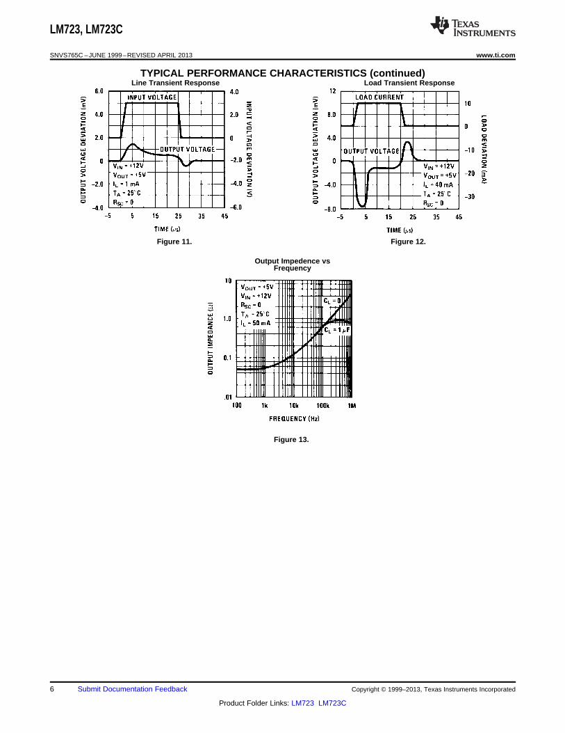
TYPICAL PERFORMANCE CHARACTERISTICS (continued)Line Transient Response Load Transient Response
Figure 11. Figure 12.
Output Impedence vsFrequency
Figure 13.
6 Submit Documentation Feedback Copyright © 1999–2013, Texas Instruments Incorporated
Product Folder Links: LM723 LM723C

LM723, LM723C
www.ti.com SNVS765C –JUNE 1999–REVISED APRIL 2013
MAXIMUM POWER RATINGS
Noisevs
Filter Capacitor LM723(CREF in Circuit of Figure 4) Power Dissipation vs
(Bandwidth 100 Hz to 10 kHz) Ambient Temperature
Figure 14. Figure 15.
LM723CPower Dissipation vsAmbient Temperature
Figure 16.
Copyright © 1999–2013, Texas Instruments Incorporated Submit Documentation Feedback 7
Product Folder Links: LM723 LM723C
LM723, LM723C
SNVS765C –JUNE 1999–REVISED APRIL 2013 www.ti.com
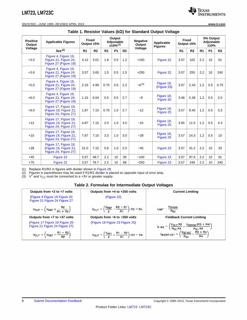
Table 1. Resistor Values (kΩ) for Standard Output Voltage
Output 5% OutputFixed FixedPositive NegativeApplicable Figures Adjustable AdjustableApplicableOutput ±5% Output ±5%Output Output±10% (1) ±10%FiguresVoltage VoltageSee (2) R1 R2 R1 P1 R2 R1 R2 R1 P1 R2
Figure 4, Figure 19,+3.0 Figure 21, Figure 24, 4.12 3.01 1.8 0.5 1.2 +100 Figure 22 3.57 102 2.2 10 91
Figure 27 (Figure 19)
Figure 4, Figure 19,+3.6 Figure 21, Figure 24, 3.57 3.65 1.5 0.5 1.5 +250 Figure 22 3.57 255 2.2 10 240
Figure 27 (Figure 19)
Figure 4, Figure 19, Figure 18,+5.0 Figure 21, Figure 24, 2.15 4.99 0.75 0.5 2.2 −6 (3) 3.57 2.43 1.2 0.5 0.75(Figure 25)Figure 27 (Figure 19)
Figure 4, Figure 19, Figure 18,+6.0 Figure 21, Figure 24, 1.15 6.04 0.5 0.5 2.7 −9 3.48 5.36 1.2 0.5 2.0Figure 25Figure 27 (Figure 19)
Figure 17, Figure 19, Figure 18,+9.0 (Figure 19, Figure 21, 1.87 7.15 0.75 1.0 2.7 −12 3.57 8.45 1.2 0.5 3.3Figure 25Figure 24, Figure 27)
Figure 17, Figure 19, Figure 18,+12 (Figure 19, Figure 21, 4.87 7.15 2.0 1.0 3.0 −15 3.65 11.5 1.2 0.5 4.3Figure 25Figure 24, Figure 27)
Figure 17, Figure 19, Figure 18,+15 (Figure 19, Figure 21, 7.87 7.15 3.3 1.0 3.0 −28 3.57 24.3 1.2 0.5 10Figure 25Figure 24, Figure 27)
Figure 17, Figure 19,+28 (Figure 19, Figure 21, 21.0 7.15 5.6 1.0 2.0 −45 Figure 23 3.57 41.2 2.2 10 33
Figure 24, Figure 27)
+45 Figure 22 3.57 48.7 2.2 10 39 −100 Figure 23 3.57 97.6 2.2 10 91
+75 Figure 22 3.57 78.7 2.2 10 68 −250 Figure 23 3.57 249 2.2 10 240
(1) Replace R1/R2 in figures with divider shown in Figure 28.(2) Figures in parentheses may be used if R1/R2 divider is placed on opposite input of error amp.(3) V+ and VCC must be connected to a +3V or greater supply.
Table 2. Formulae for Intermediate Output Voltages
Outputs from +2 to +7 volts Outputs from +4 to +250 volts Current Limiting
(Figure 4 Figure 19 Figure 20 (Figure 22)Figure 21 Figure 24 Figure 27
Outputs from +7 to +37 volts Outputs from −6 to −250 volts Foldback Current Limiting
(Figure 17 Figure 19 Figure 20 (Figure 18 Figure 23 Figure 25)Figure 21 Figure 24 Figure 27)
8 Submit Documentation Feedback Copyright © 1999–2013, Texas Instruments Incorporated
Product Folder Links: LM723 LM723C
LM723, LM723C
www.ti.com SNVS765C –JUNE 1999–REVISED APRIL 2013
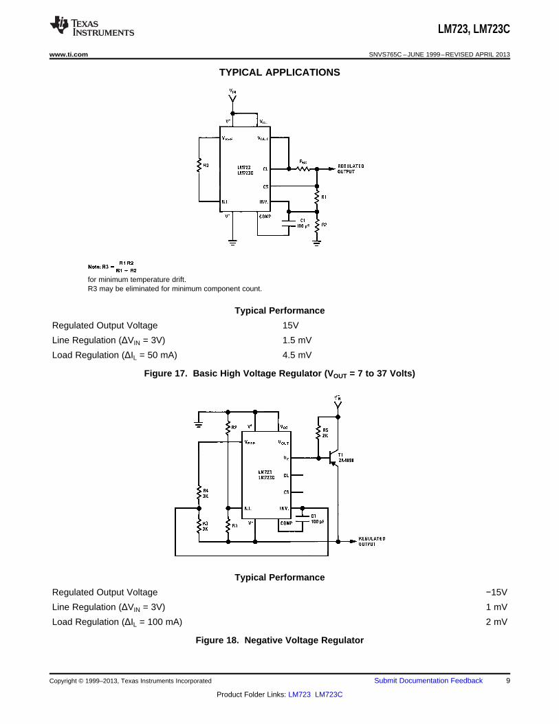
TYPICAL APPLICATIONS
for minimum temperature drift.R3 may be eliminated for minimum component count.
Typical Performance
Regulated Output Voltage 15V
Line Regulation (ΔVIN = 3V) 1.5 mV
Load Regulation (ΔIL = 50 mA) 4.5 mV
Figure 17. Basic High Voltage Regulator (VOUT = 7 to 37 Volts)
Typical Performance
Regulated Output Voltage −15V
Line Regulation (ΔVIN = 3V) 1 mV
Load Regulation (ΔIL = 100 mA) 2 mV
Figure 18. Negative Voltage Regulator
Copyright © 1999–2013, Texas Instruments Incorporated Submit Documentation Feedback 9
Product Folder Links: LM723 LM723C
LM723, LM723C
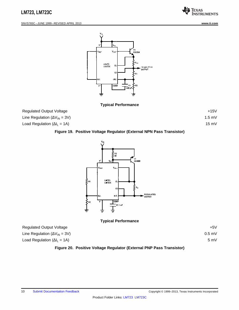
SNVS765C –JUNE 1999–REVISED APRIL 2013 www.ti.com
Typical Performance
Regulated Output Voltage +15V
Line Regulation (ΔVIN = 3V) 1.5 mV
Load Regulation (ΔIL = 1A) 15 mV
Figure 19. Positive Voltage Regulator (External NPN Pass Transistor)
Typical Performance
Regulated Output Voltage +5V
Line Regulation (ΔVIN = 3V) 0.5 mV
Load Regulation (ΔIL = 1A) 5 mV
Figure 20. Positive Voltage Regulator (External PNP Pass Transistor)
10 Submit Documentation Feedback Copyright © 1999–2013, Texas Instruments Incorporated
Product Folder Links: LM723 LM723C
LM723, LM723C
www.ti.com SNVS765C –JUNE 1999–REVISED APRIL 2013
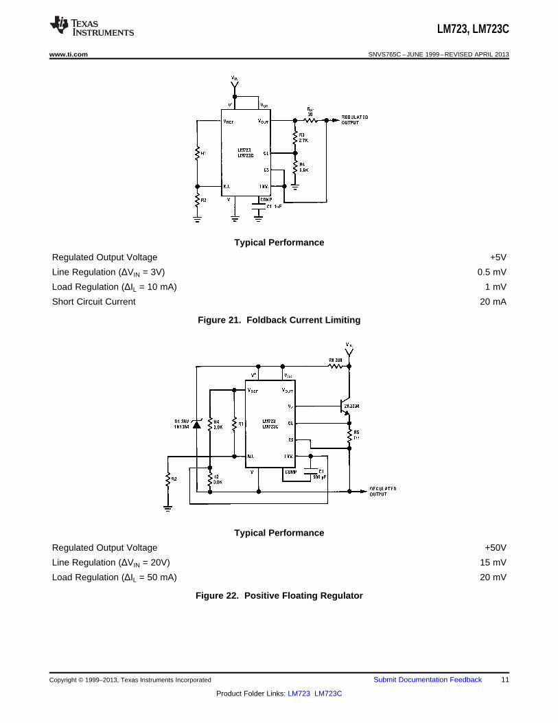
Typical Performance
Regulated Output Voltage +5V
Line Regulation (ΔVIN = 3V) 0.5 mV
Load Regulation (ΔIL = 10 mA) 1 mV
Short Circuit Current 20 mA
Figure 21. Foldback Current Limiting
Typical Performance
Regulated Output Voltage +50V
Line Regulation (ΔVIN = 20V) 15 mV
Load Regulation (ΔIL = 50 mA) 20 mV
Figure 22. Positive Floating Regulator
Copyright © 1999–2013, Texas Instruments Incorporated Submit Documentation Feedback 11
Product Folder Links: LM723 LM723C
LM723, LM723C
SNVS765C –JUNE 1999–REVISED APRIL 2013 www.ti.com
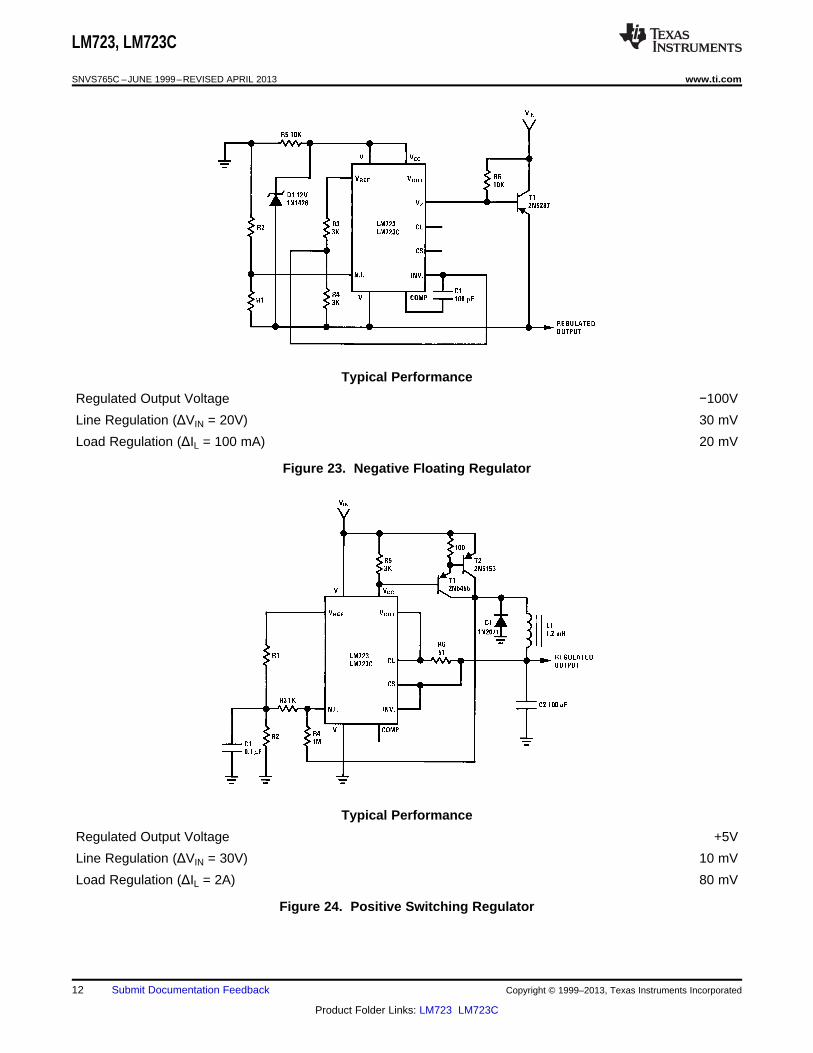
Typical Performance
Regulated Output Voltage −100V
Line Regulation (ΔVIN = 20V) 30 mV
Load Regulation (ΔIL = 100 mA) 20 mV
Figure 23. Negative Floating Regulator
Typical Performance
Regulated Output Voltage +5V
Line Regulation (ΔVIN = 30V) 10 mV
Load Regulation (ΔIL = 2A) 80 mV
Figure 24. Positive Switching Regulator
12 Submit Documentation Feedback Copyright © 1999–2013, Texas Instruments Incorporated
Product Folder Links: LM723 LM723C
LM723, LM723C
www.ti.com SNVS765C –JUNE 1999–REVISED APRIL 2013
Typical Performance
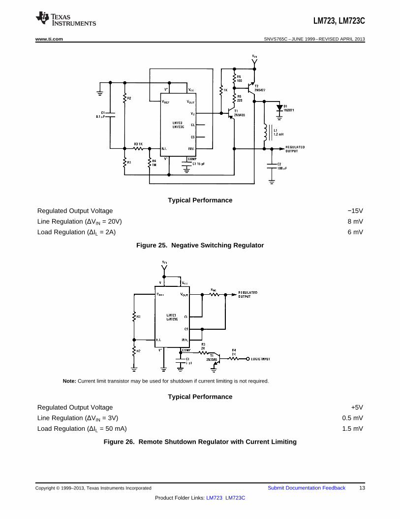
Regulated Output Voltage −15V
Line Regulation (ΔVIN = 20V) 8 mV
Load Regulation (ΔIL = 2A) 6 mV
Figure 25. Negative Switching Regulator
Note: Current limit transistor may be used for shutdown if current limiting is not required.
Typical Performance
Regulated Output Voltage +5V
Line Regulation (ΔVIN = 3V) 0.5 mV
Load Regulation (ΔIL = 50 mA) 1.5 mV
Figure 26. Remote Shutdown Regulator with Current Limiting
Copyright © 1999–2013, Texas Instruments Incorporated Submit Documentation Feedback 13
Product Folder Links: LM723 LM723C
LM723, LM723C
SNVS765C –JUNE 1999–REVISED APRIL 2013 www.ti.com
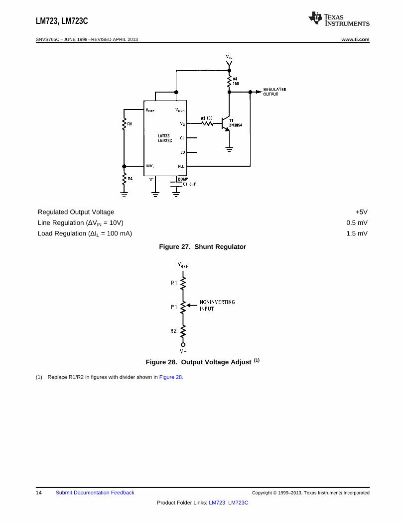
Regulated Output Voltage +5V
Line Regulation (ΔVIN = 10V) 0.5 mV
Load Regulation (ΔIL = 100 mA) 1.5 mV
Figure 27. Shunt Regulator
Figure 28. Output Voltage Adjust (1)
(1) Replace R1/R2 in figures with divider shown in Figure 28.
14 Submit Documentation Feedback Copyright © 1999–2013, Texas Instruments Incorporated
Product Folder Links: LM723 LM723C

LM723, LM723C
www.ti.com SNVS765C –JUNE 1999–REVISED APRIL 2013
Schematic Diagram
Copyright © 1999–2013, Texas Instruments Incorporated Submit Documentation Feedback 15
Product Folder Links: LM723 LM723C
LM723, LM723C
SNVS765C –JUNE 1999–REVISED APRIL 2013 www.ti.com
REVISION HISTORY
Changes from Revision B (April 2013) to Revision C Page
• Changed layout of National Data Sheet to TI format .......................................................................................................... 15
16 Submit Documentation Feedback Copyright © 1999–2013, Texas Instruments Incorporated
Product Folder Links: LM723 LM723C
PACKAGE OPTION ADDENDUM
www.ti.com 25-Aug-2017
Addendum-Page 1
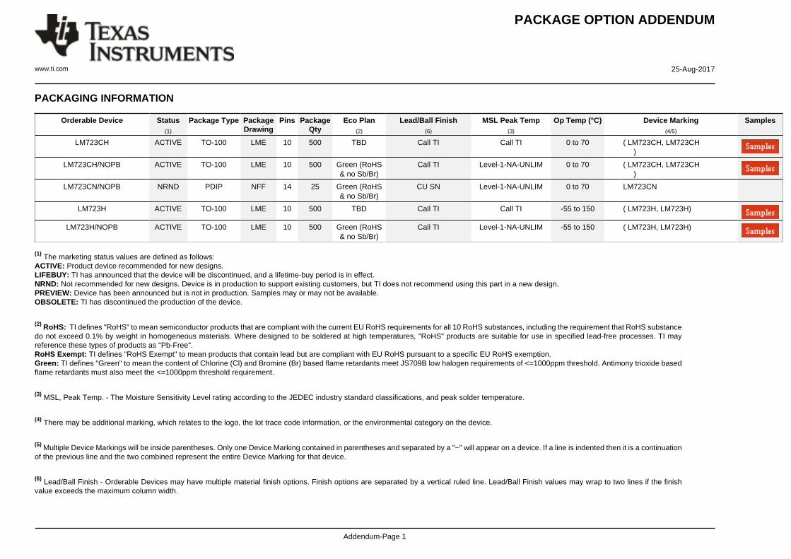
PACKAGING INFORMATION
Orderable Device Status(1)
Package Type PackageDrawing
Pins PackageQty
Eco Plan(2)
Lead/Ball Finish(6)
MSL Peak Temp(3)
Op Temp (°C) Device Marking(4/5)
Samples
LM723CH ACTIVE TO-100 LME 10 500 TBD Call TI Call TI 0 to 70 ( LM723CH, LM723CH )
LM723CH/NOPB ACTIVE TO-100 LME 10 500 Green (RoHS& no Sb/Br)
Call TI Level-1-NA-UNLIM 0 to 70 ( LM723CH, LM723CH )
LM723CN/NOPB NRND PDIP NFF 14 25 Green (RoHS& no Sb/Br)
CU SN Level-1-NA-UNLIM 0 to 70 LM723CN
LM723H ACTIVE TO-100 LME 10 500 TBD Call TI Call TI -55 to 150 ( LM723H, LM723H)
LM723H/NOPB ACTIVE TO-100 LME 10 500 Green (RoHS& no Sb/Br)
Call TI Level-1-NA-UNLIM -55 to 150 ( LM723H, LM723H)
(1) The marketing status values are defined as follows:ACTIVE: Product device recommended for new designs.LIFEBUY: TI has announced that the device will be discontinued, and a lifetime-buy period is in effect.NRND: Not recommended for new designs. Device is in production to support existing customers, but TI does not recommend using this part in a new design.PREVIEW: Device has been announced but is not in production. Samples may or may not be available.OBSOLETE: TI has discontinued the production of the device.
(2) RoHS: TI defines "RoHS" to mean semiconductor products that are compliant with the current EU RoHS requirements for all 10 RoHS substances, including the requirement that RoHS substancedo not exceed 0.1% by weight in homogeneous materials. Where designed to be soldered at high temperatures, "RoHS" products are suitable for use in specified lead-free processes. TI mayreference these types of products as "Pb-Free".RoHS Exempt: TI defines "RoHS Exempt" to mean products that contain lead but are compliant with EU RoHS pursuant to a specific EU RoHS exemption.Green: TI defines "Green" to mean the content of Chlorine (Cl) and Bromine (Br) based flame retardants meet JS709B low halogen requirements of <=1000ppm threshold. Antimony trioxide basedflame retardants must also meet the <=1000ppm threshold requirement.
(3) MSL, Peak Temp. - The Moisture Sensitivity Level rating according to the JEDEC industry standard classifications, and peak solder temperature.
(4) There may be additional marking, which relates to the logo, the lot trace code information, or the environmental category on the device.
(5) Multiple Device Markings will be inside parentheses. Only one Device Marking contained in parentheses and separated by a "~" will appear on a device. If a line is indented then it is a continuationof the previous line and the two combined represent the entire Device Marking for that device.
(6) Lead/Ball Finish - Orderable Devices may have multiple material finish options. Finish options are separated by a vertical ruled line. Lead/Ball Finish values may wrap to two lines if the finishvalue exceeds the maximum column width.
PACKAGE OPTION ADDENDUM
www.ti.com 25-Aug-2017
Addendum-Page 2
Important Information and Disclaimer:The information provided on this page represents TI's knowledge and belief as of the date that it is provided. TI bases its knowledge and belief on informationprovided by third parties, and makes no representation or warranty as to the accuracy of such information. Efforts are underway to better integrate information from third parties. TI has taken andcontinues to take reasonable steps to provide representative and accurate information but may not have conducted destructive testing or chemical analysis on incoming materials and chemicals.TI and TI suppliers consider certain information to be proprietary, and thus CAS numbers and other limited information may not be available for release.
In no event shall TI's liability arising out of such information exceed the total purchase price of the TI part(s) at issue in this document sold by TI to Customer on an annual basis.
www.ti.com
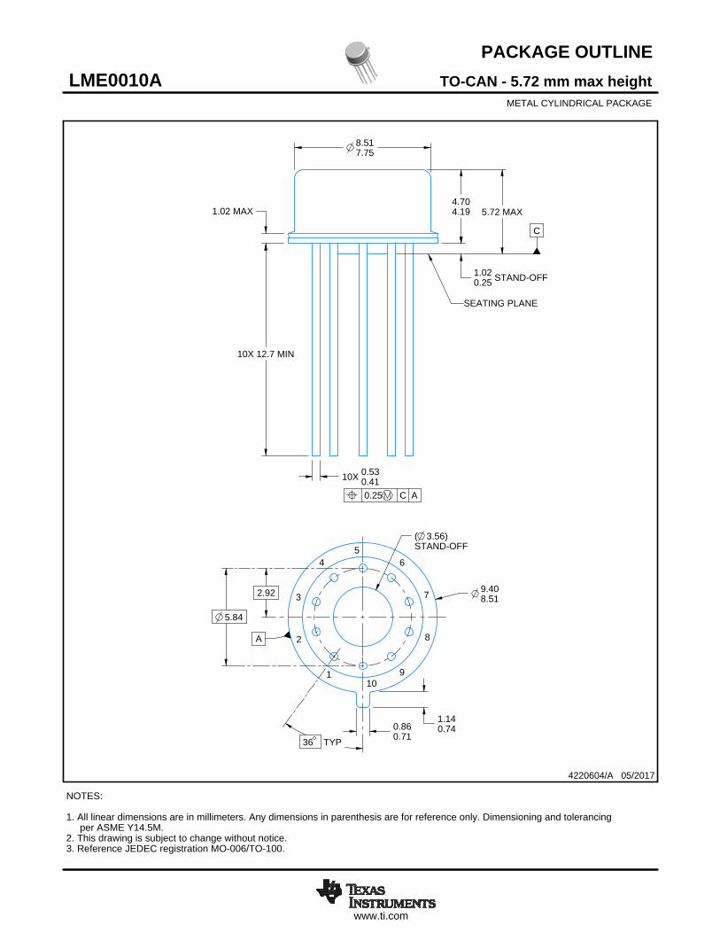
PACKAGE OUTLINE
C
A
9.408.51
( 3.56)STAND-OFF
0.860.71
5.84
2.92
8.517.75
5.72 MAX4.704.191.02 MAX
10X 12.7 MIN
10X 0.530.41
STAND-OFF1.020.25
1.140.74
36 TYP
TO-CAN - 5.72 mm max heightLME0010AMETAL CYLINDRICAL PACKAGE
4220604/A 05/2017
NOTES: 1. All linear dimensions are in millimeters. Any dimensions in parenthesis are for reference only. Dimensioning and tolerancing per ASME Y14.5M.2. This drawing is subject to change without notice.3. Reference JEDEC registration MO-006/TO-100.
0.25 C A
SEATING PLANE
1
2
3
45
6
7
10
8
9
SCALE 0.800
www.ti.com
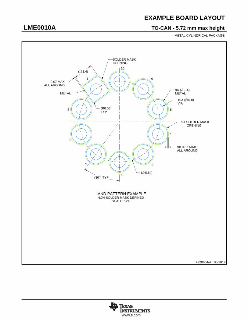
EXAMPLE BOARD LAYOUT
0.07 MAXALL AROUND
9X 0.07 MAXALL AROUND
( 5.84)
( 1.4)
9X ( 1.4)METAL
10X ( 0.8)VIA
(R0.05)TYP
(36 ) TYP
TO-CAN - 5.72 mm max heightLME0010AMETAL CYLINDRICAL PACKAGE
4220604/A 05/2017
LAND PATTERN EXAMPLENON-SOLDER MASK DEFINED
SCALE: 12X
9X SOLDER MASK OPENING
SOLDER MASKOPENING
METAL
1
2
3
4
5
6
7
10
8
9
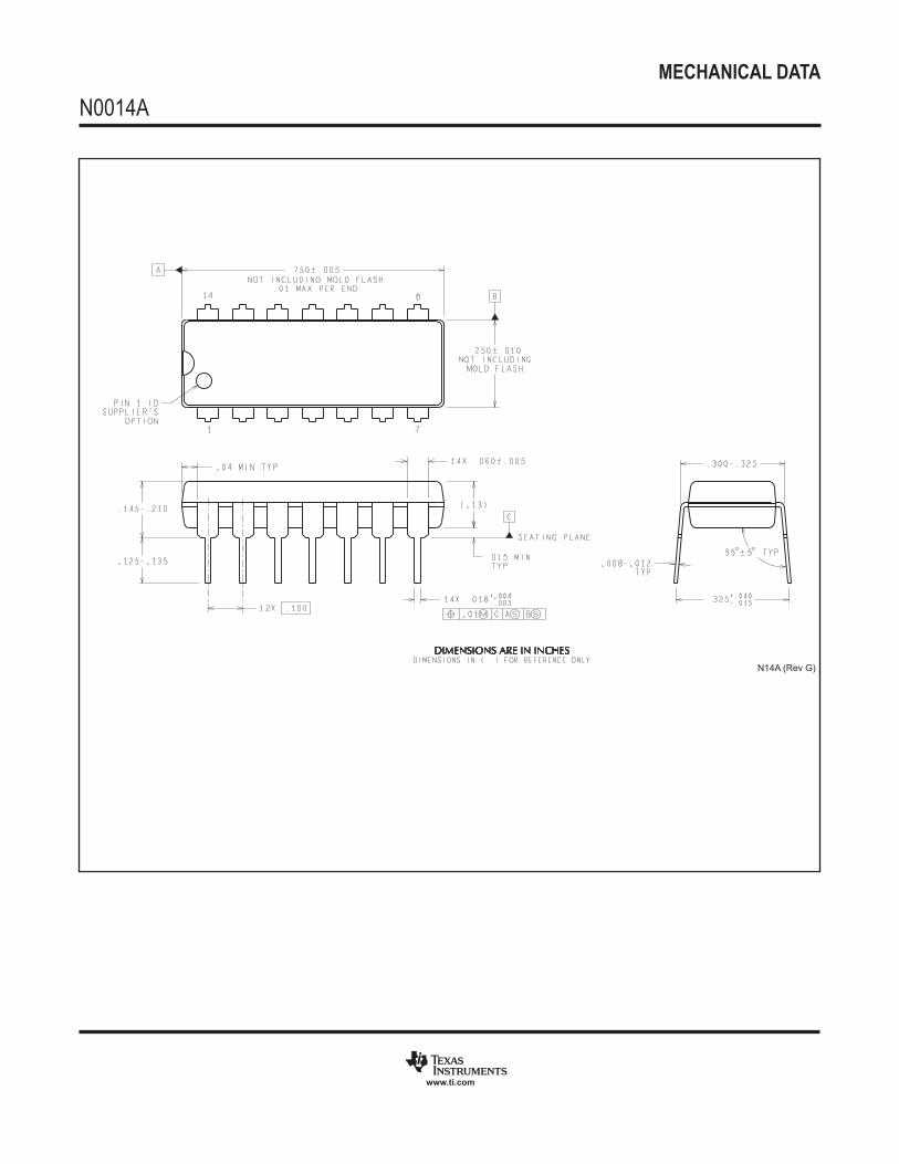
MECHANICAL DATA
N0014A
www.ti.com
N14A (Rev G)
IMPORTANT NOTICE
Texas Instruments Incorporated (TI) reserves the right to make corrections, enhancements, improvements and other changes to itssemiconductor products and services per JESD46, latest issue, and to discontinue any product or service per JESD48, latest issue. Buyersshould obtain the latest relevant information before placing orders and should verify that such information is current and complete.TI’s published terms of sale for semiconductor products (http://www.ti.com/sc/docs/stdterms.htm) apply to the sale of packaged integratedcircuit products that TI has qualified and released to market. Additional terms may apply to the use or sale of other types of TI products andservices.Reproduction of significant portions of TI information in TI data sheets is permissible only if reproduction is without alteration and isaccompanied by all associated warranties, conditions, limitations, and notices. TI is not responsible or liable for such reproduceddocumentation. Information of third parties may be subject to additional restrictions. Resale of TI products or services with statementsdifferent from or beyond the parameters stated by TI for that product or service voids all express and any implied warranties for theassociated TI product or service and is an unfair and deceptive business practice. TI is not responsible or liable for any such statements.Buyers and others who are developing systems that incorporate TI products (collectively, “Designers”) understand and agree that Designersremain responsible for using their independent analysis, evaluation and judgment in designing their applications and that Designers havefull and exclusive responsibility to assure the safety of Designers' applications and compliance of their applications (and of all TI productsused in or for Designers’ applications) with all applicable regulations, laws and other applicable requirements. Designer represents that, withrespect to their applications, Designer has all the necessary expertise to create and implement safeguards that (1) anticipate dangerousconsequences of failures, (2) monitor failures and their consequences, and (3) lessen the likelihood of failures that might cause harm andtake appropriate actions. Designer agrees that prior to using or distributing any applications that include TI products, Designer willthoroughly test such applications and the functionality of such TI products as used in such applications.TI’s provision of technical, application or other design advice, quality characterization, reliability data or other services or information,including, but not limited to, reference designs and materials relating to evaluation modules, (collectively, “TI Resources”) are intended toassist designers who are developing applications that incorporate TI products; by downloading, accessing or using TI Resources in anyway, Designer (individually or, if Designer is acting on behalf of a company, Designer’s company) agrees to use any particular TI Resourcesolely for this purpose and subject to the terms of this Notice.TI’s provision of TI Resources does not expand or otherwise alter TI’s applicable published warranties or warranty disclaimers for TIproducts, and no additional obligations or liabilities arise from TI providing such TI Resources. TI reserves the right to make corrections,enhancements, improvements and other changes to its TI Resources. TI has not conducted any testing other than that specificallydescribed in the published documentation for a particular TI Resource.Designer is authorized to use, copy and modify any individual TI Resource only in connection with the development of applications thatinclude the TI product(s) identified in such TI Resource. NO OTHER LICENSE, EXPRESS OR IMPLIED, BY ESTOPPEL OR OTHERWISETO ANY OTHER TI INTELLECTUAL PROPERTY RIGHT, AND NO LICENSE TO ANY TECHNOLOGY OR INTELLECTUAL PROPERTYRIGHT OF TI OR ANY THIRD PARTY IS GRANTED HEREIN, including but not limited to any patent right, copyright, mask work right, orother intellectual property right relating to any combination, machine, or process in which TI products or services are used. Informationregarding or referencing third-party products or services does not constitute a license to use such products or services, or a warranty orendorsement thereof. Use of TI Resources may require a license from a third party under the patents or other intellectual property of thethird party, or a license from TI under the patents or other intellectual property of TI.TI RESOURCES ARE PROVIDED “AS IS” AND WITH ALL FAULTS. TI DISCLAIMS ALL OTHER WARRANTIES ORREPRESENTATIONS, EXPRESS OR IMPLIED, REGARDING RESOURCES OR USE THEREOF, INCLUDING BUT NOT LIMITED TOACCURACY OR COMPLETENESS, TITLE, ANY EPIDEMIC FAILURE WARRANTY AND ANY IMPLIED WARRANTIES OFMERCHANTABILITY, FITNESS FOR A PARTICULAR PURPOSE, AND NON-INFRINGEMENT OF ANY THIRD PARTY INTELLECTUALPROPERTY RIGHTS. TI SHALL NOT BE LIABLE FOR AND SHALL NOT DEFEND OR INDEMNIFY DESIGNER AGAINST ANY CLAIM,INCLUDING BUT NOT LIMITED TO ANY INFRINGEMENT CLAIM THAT RELATES TO OR IS BASED ON ANY COMBINATION OFPRODUCTS EVEN IF DESCRIBED IN TI RESOURCES OR OTHERWISE. IN NO EVENT SHALL TI BE LIABLE FOR ANY ACTUAL,DIRECT, SPECIAL, COLLATERAL, INDIRECT, PUNITIVE, INCIDENTAL, CONSEQUENTIAL OR EXEMPLARY DAMAGES INCONNECTION WITH OR ARISING OUT OF TI RESOURCES OR USE THEREOF, AND REGARDLESS OF WHETHER TI HAS BEENADVISED OF THE POSSIBILITY OF SUCH DAMAGES.Unless TI has explicitly designated an individual product as meeting the requirements of a particular industry standard (e.g., ISO/TS 16949and ISO 26262), TI is not responsible for any failure to meet such industry standard requirements.Where TI specifically promotes products as facilitating functional safety or as compliant with industry functional safety standards, suchproducts are intended to help enable customers to design and create their own applications that meet applicable functional safety standardsand requirements. Using products in an application does not by itself establish any safety features in the application. Designers mustensure compliance with safety-related requirements and standards applicable to their applications. Designer may not use any TI products inlife-critical medical equipment unless authorized officers of the parties have executed a special contract specifically governing such use.Life-critical medical equipment is medical equipment where failure of such equipment would cause serious bodily injury or death (e.g., lifesupport, pacemakers, defibrillators, heart pumps, neurostimulators, and implantables). Such equipment includes, without limitation, allmedical devices identified by the U.S. Food and Drug Administration as Class III devices and equivalent classifications outside the U.S.TI may expressly designate certain products as completing a particular qualification (e.g., Q100, Military Grade, or Enhanced Product).Designers agree that it has the necessary expertise to select the product with the appropriate qualification designation for their applicationsand that proper product selection is at Designers’ own risk. Designers are solely responsible for compliance with all legal and regulatoryrequirements in connection with such selection.Designer will fully indemnify TI and its representatives against any damages, costs, losses, and/or liabilities arising out of Designer’s non-compliance with the terms and provisions of this Notice.
Mailing Address: Texas Instruments, Post Office Box 655303, Dallas, Texas 75265Copyright © 2017, Texas Instruments Incorporated