Embed Size (px)
Citation preview

Solder Joint Inspection& Process Defects
Bob Willis
Electronics Academy Webinar Presenter
Your Delegate Webinar Control Panel
Open and close your panelFull screen view
Submit text questionsduring or at the end
Welcome to the Vision EngineeringElectronics Academy Webinar whichwill start at 2.30pmUK Time

FREEElectronics Academy Webinar Series
The Electronics Academy Webinar Series takes an in‐depth look at the issuesaffecting PCB/SMT assembly and the challenges of achieving Zero DefectManufacture. Understand the common causes of solder joint failure and learn howto identify and rectify process defects – improving quality and reducing costs
Learn expert tips to identify quality issuesUnderstand the common causes of process failuresA convenient and quick way to update your skills
In the future have access to a video library of online training sessions
Vision Engineering Ltd is a global leading‐edge manufacturer ofunique ergonomic stereo microscopes and non‐contact measuringsystems
Since its formation in 1958, Vision Engineering has become one ofthe world's most innovative and dynamic microscopemanufacturers, with offices across Europe, Asia and NorthAmerica, as well as a fully trained global distribution network
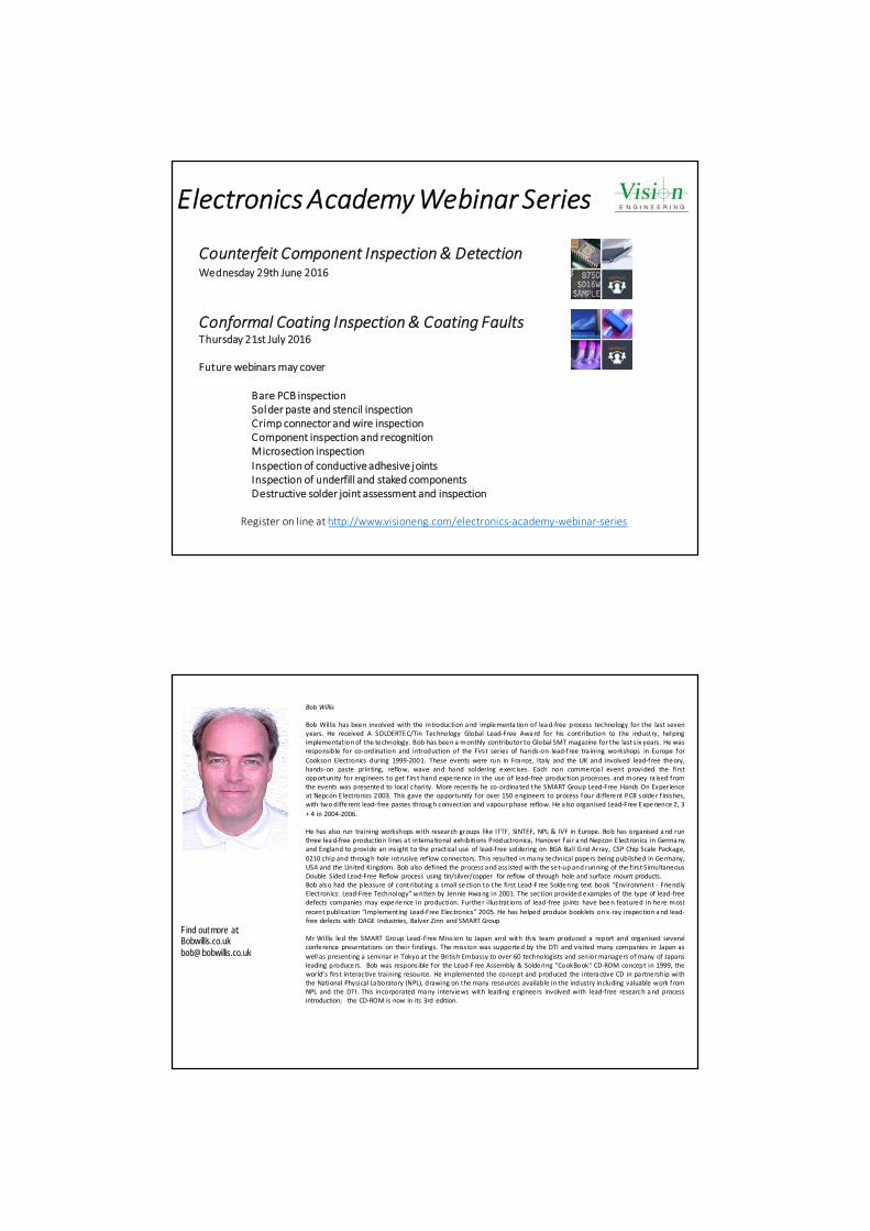
Electronics Academy Webinar Series
Counterfeit Component Inspection & DetectionWednesday 29th June 2016
Conformal Coating Inspection & Coating FaultsThursday 21st July 2016
Future webinars may cover
Bare PCB inspectionSolder paste and stencil inspectionCrimp connector and wire inspectionComponent inspection and recognitionMicrosection inspectionInspection of conductive adhesive jointsInspection of underfill and staked componentsDestructive solder joint assessment and inspection
Register on line at http://www.visioneng.com/electronics‐academy‐webinar‐series
Bob Willis
Bob Willis has been involved with the introduction and implementa tion of lead‐free process technology for the last sevenyears. He received A SOLDERTEC/Tin Technology Global Lead‐Free Award for his contribution to the industry, helpingimplementation of the technology. Bob has been a monthly contributor to Global SMT magazine for the last s ix years. He wasresponsible for co‐ordination and introduction of the Firs t series of hands‐on lead‐free tra ining workshops in Europe for
Cookson Electronics during 1999‐2001. These events were run in France, Italy and the UK and involved lead‐free theory,hands‐on paste printing, reflow, wave and hand soldering exercises. Each non commercia l event provided the firstopportunity for engineers to get f irs t hand experience in the use of lead‐free production processes and money ra ised fromthe events was presented to local charity. More recently he co‐ordina ted the SMART Group Lead‐Free Hands On Experienceat Nepcon E lectronics 2003. This gave the opportunity for over 150 engineers to process four different PCB solder f inishes,with two different lead‐free pastes through convection and vapour phase reflow. He a lso organised Lead‐Free Experience 2, 3
+ 4 in 2004‐2006.
He has also run training workshops with research groups like ITTF, SINTEF, NPL & IVF in Europe. Bob has organised and runthree lead‐free production lines a t interna tional exhibitions Productronica, Hanover Fair and Nepcon E lectronics in Germanyand England to provide an ins ight to the practical use of lead‐free soldering on BGA Ball Grid Array, CSP Chip Scale Package,
0210 chip and through hole intrusive ref low connectors. This resulted inmany technical papers being published in Germany,USA and the United Kingdom. Bob also defined the process and ass isted with the set‐up and running of the f irs t SimultaneousDouble Sided Lead‐Free Reflow process using tin/silver/copper for reflow of through hole and surface mount products.Bob also had the pleasure of contributing a small section to the first Lead‐F ree Soldering text book “Environment ‐ FriendlyElectronics: Lead‐Free Technology” written by Jennie Hwang in 2001. The section provided examples of the type of lead‐freedefects companies may experience in production. Further illus trations of lead‐free joints have been featured in here most
recent publication “Implementing Lead‐Free Electronics” 2005. He has helped produce booklets on x‐ray inspection and lead‐free defects with DAGE Industries, Balver Zinn and SMART Group
Mr Willis led the SMART Group Lead‐Free Miss ion to Japan and with this team produced a report and organised severalconference presentations on their f indings. The miss ion was supported by the DTI and vis ited many companies in Japan as
well as presenting a seminar in Tokyo at the British Embassy to over 60 technologists and seniormanagers of many of Japansleading producers. Bob was respons ible for the Lead‐F ree Assembly & Soldering "CookBook" CD‐ROM concept in 1999, theworld’s firs t interactive training resource. He implemented the concept and produced the interactive CD in partnership withthe National Physical Laboratory (NPL), drawing on the many resources available in the industry including valuable work fromNPL and the DTI. This incorporated many interviews with leading engineers involved with lead‐free research and processintroduction; the CD‐ROM is now in its 3rd edition.
Find out more at:[email protected]
Bob Willis currently operates a training and consultancy business based in England. Bob is a member of the SMART Technical Committee.Although a specialist for companies implementing Surface Mount Technology Mr Willis provides training and consultancy in most areas ofelectronic manufacture. He has worked with the GEC Technical Directorate as Surface Mount Co-Coordinator for both the Marconi and GECgroup of companies and prior to that he was Senior Process Control Engineer with Marconi Communication Systems, where he had workedsince his apprenticeship. Following his time with GEC he became Technical Director of an electronics contract manufacturing companywhere he formed a successful training and consultancy division.
As a process engineer, he was involved in all aspects of electronic production and assembly involved in setting up production processes andevaluating materials; this also involved obtaining company approval on a wide range of Marconi's processes and products including printedcircuit board manufacture. During the period with Marconi, experience was gained in methods and equipment for environmental testing ofcomponents, printed boards and assemblies with an interest developed in many areas of defect analysis. Over the last 15 years he hasbeen involved in all aspects of surface mounted assembly, both at production and quality level and during that time has been involved intraining staff and other engineers in many aspects of modern production.
Over the past few years Mr. Willis has travelled in the United States, Japan, China, New Zealand, Australia and the Far East looking atareas of electronics and lecturing on electronic assembly. Mr. Willis was presented with the Paul Eisler award by the IMF (Institute of MetalFinishing) for the best technical paper during their technical programmes. He has conducted SMT Training programs for Texas Instrumentsand is currently course leader for Reflow and Wave Soldering Workshops in the United Kingdom. Mr Willis is an IEE Registered Trainer andhas been responsible for training courses run by the PCIF originally one of Europe's largest printed circuit associations. Bob has conductedworkshops with all the major organisations and exhibition organisers World Wide and is known for being an entertaining presenter and theonly presenter to use unique process video clips during his workshops to demonstrate each point made. Bob has written two book which arefree to download on line, Design & Assembly with Pin In Hole Intrusive Reflow & Package On Package Design, Assembly andInspection
Mr. Willis was Chairman of the SMART Group, European Surface Mount Trade Association from 1990-94 and has been elected HonoraryLife President and currently holds the position of SMART Group Technical Director, he also works on BSI Standards Working Parties. He isa Fellow of the Insti tute Circuit Technology, an NVQ Assessor, Member of the Institute of Quality Assurance and Society of EnvironmentalTest Engineers. Bob Willis currently writes regular features for AMT Ireland, Asian Electronics Engineer and Circuits Assembly the USmagazine. He also is responsible for writing each of the SMART Group Charity Technology reports, which are sold in Europe and Americaby the SMTA to raise money for worthy causes. Bob ran the SMART Group PPM Monitoring Project in the United Kingdom supported by theDepartment of Trade and Industry. He was coordinator of the LEADOUT Project for SMART Group. LEADOUT was one of the largest EUfunded projects, currently he is coordinating European projects TestPEP, uBGA and ChipCheck
In September 2015 Bob voted the Best Speaker at SMTA International Conference in Chicago
Find out more at:[email protected]
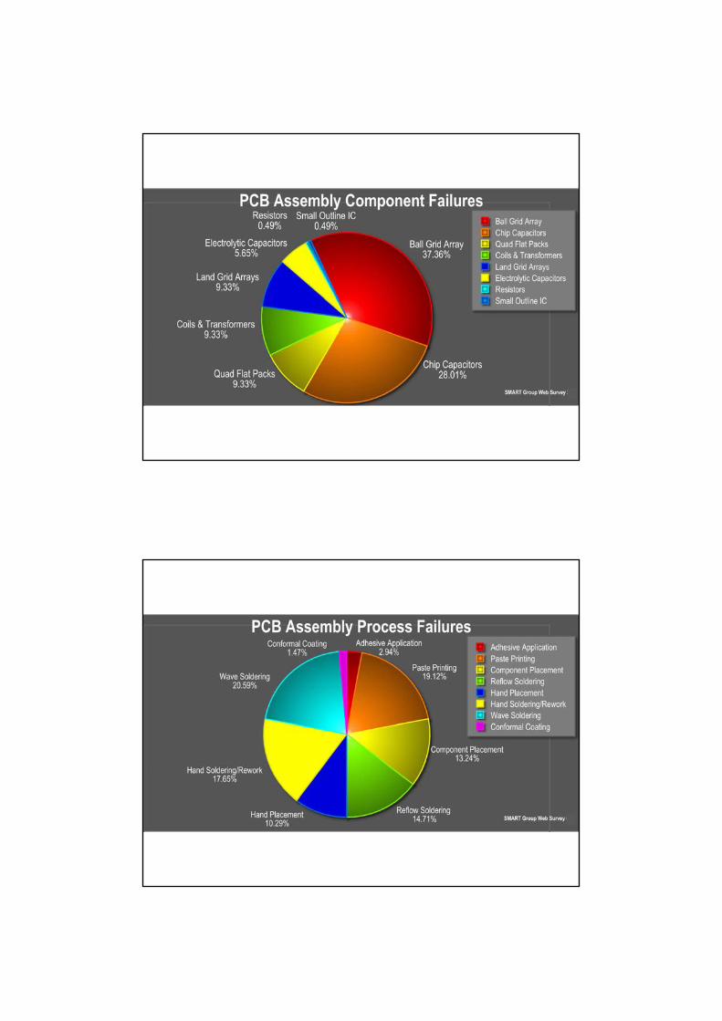
Printed Circuit Board Defects

International Inspection Standards
IPC 600 H IPC 610 E IPC 620 B
IPC J‐STD‐001 ‐ Requirements for Soldered Electrical and Electronic Assemblies
International Inspection Standards
Process Indicator

International Inspection Standards
IPC J‐STD‐001 ‐ Requirements for Soldered Electrical and Electronic Assemblies
IPC HDBK 001 & IPC 610
Other standards include:NASA, ESA & IEC
International Inspection Standards
IPC J‐STD‐001 ‐ Requirements for Soldered Electrical and Electronic Assemblies
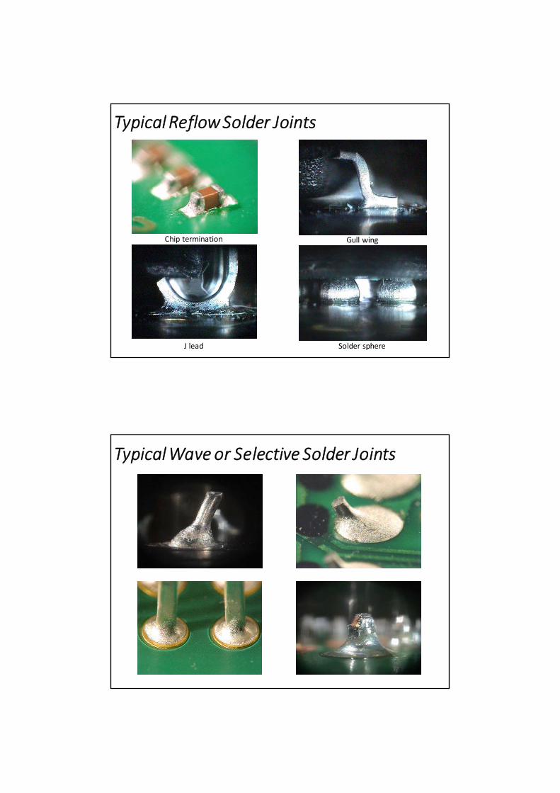
Typical Reflow Solder Joints
Chip termination Gull wing
J lead Solder sphere
Typical Wave or Selective Solder Joints
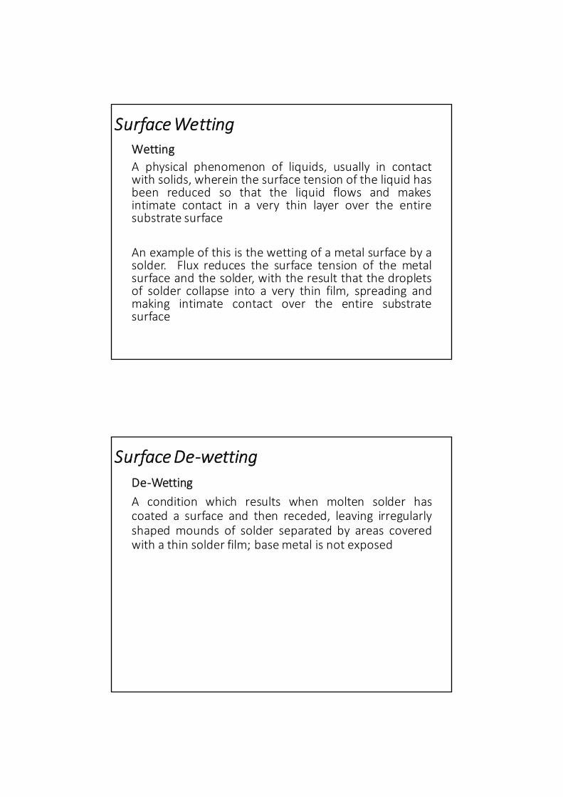
Surface WettingWetting
A physical phenomenon of liquids, usually in contactwith solids, wherein the surface tension of the liquid hasbeen reduced so that the liquid flows and makesintimate contact in a very thin layer over the entiresubstrate surface
An example of this is the wetting of a metal surface by asolder. Flux reduces the surface tension of the metalsurface and the solder, with the result that the dropletsof solder collapse into a very thin film, spreading andmaking intimate contact over the entire substratesurface
Surface De‐wetting
De‐Wetting
A condition which results when molten solder hascoated a surface and then receded, leaving irregularlyshaped mounds of solder separated by areas coveredwith a thin solder film; basemetal is not exposed
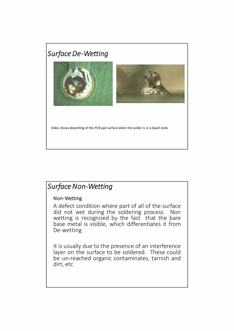
Surface De‐Wetting
Video shows dewetting of the PCB pad surface when the solder is in a liquid state
Surface Non‐Wetting
Non‐Wetting
A defect condition where part of all of the surfacedid not wet during the soldering process. Nonwetting is recognized by the fact that the barebase metal is visible, which differentiates it fromDe‐wetting
It is usually due to the presence of an interferencelayer on the surface to be soldered. These couldbe un‐reached organic contaminates, tarnish anddirt, etc
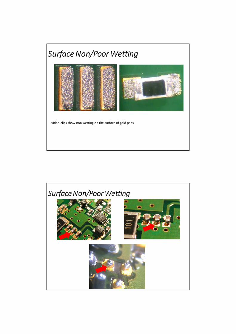
Surface Non/Poor Wetting
Video clips show non wetting on the surface of gold pads
Surface Non/Poor Wetting
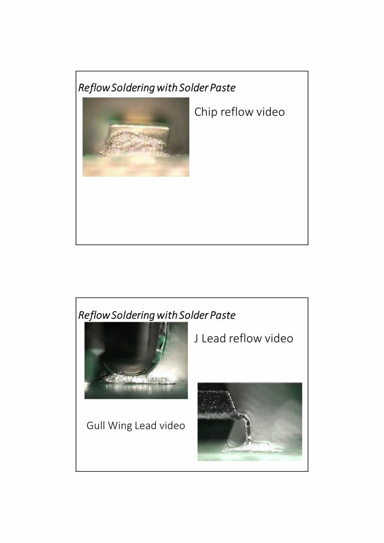
Reflow Soldering with Solder Paste
Chip reflow video
J Lead reflow video
Gull Wing Lead video
Reflow Soldering with Solder Paste
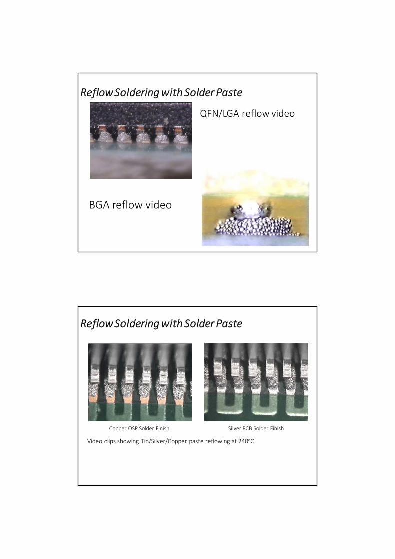
Reflow Soldering with Solder Paste
QFN/LGA reflow video
BGA reflow video
Video clips showing Tin/Silver/Copper paste reflowing at 240oC
Copper OSP Solder Finish Silver PCB Solder Finish
Reflow Soldering with Solder Paste
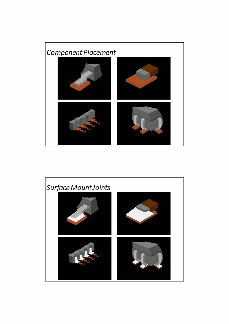
Component Placement
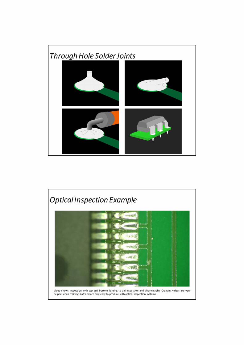
Surface Mount Joints
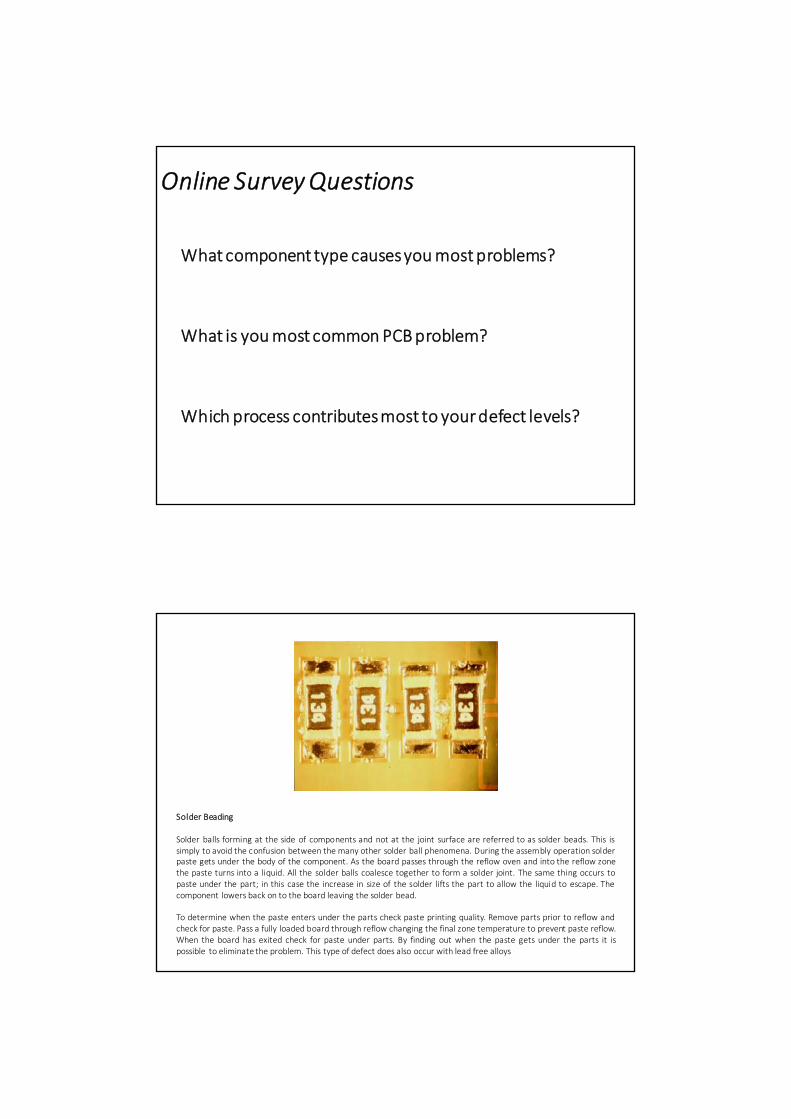
Through Hole Solder Joints
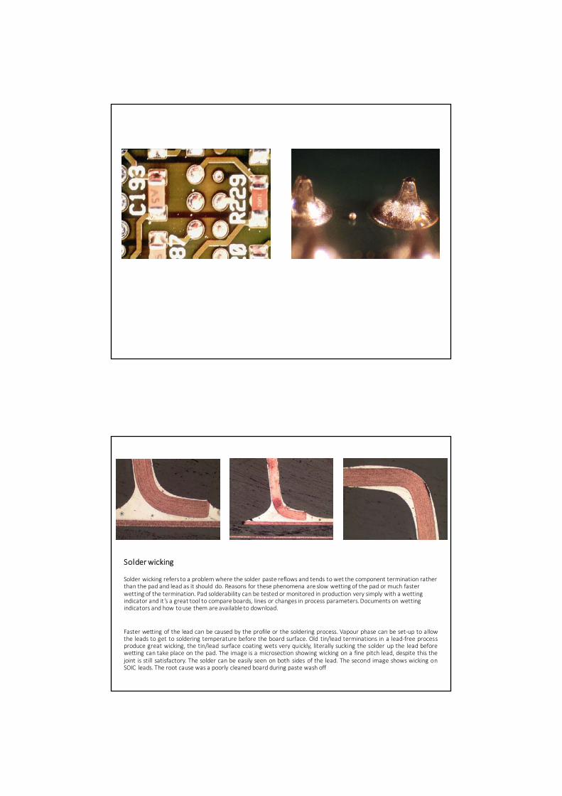
Optical Inspection Example
Video shows inspection with top and bottom lighting to aid inspection and photography. Creating videos are veryhelpful when training staff and arenow easy to produce with optical inspection systems
Online Survey Questions
What component type causes you most problems?
What is you most common PCB problem?
Which process contributes most to your defect levels?
Solder Beading
Solder balls forming at the side of components and not at the joint surface are referred to as solder beads. This issimply to avoid the confusion between the many other solder ball phenomena. During the assembly operation solderpaste gets under the body of the component. As the board passes through the reflow oven and into the reflow zonethe paste turns into a liquid. All the solder balls coalesce together to form a solder joint. The same thing occurs topaste under the part; in this case the increase in size of the solder lifts the part to allow the liquid to escape. Thecomponent lowers back on to the board leaving the solder bead.
To determine when the paste enters under the parts check paste printing quality. Remove parts prior to reflow andcheck for paste. Pass a fully loaded board through reflow changing the final zone temperature to prevent paste reflow.When the board has exited check for paste under parts. By finding out when the paste gets under the parts it ispossible to eliminate the problem. This type of defect does also occur with lead free alloys
Solder wicking
Solder wicking refers to a problem where the solder paste reflows and tends to wet the component termination rather than the pad and lead as it should do. Reasons for these phenomena are slow wetting of the pad or much faster wetting of the termination. Pad solderability can be tested or monitored in production very simply with a wetting indicator and it ’s a great tool to compare boards, lines or changes in process parameters. Documents on wetting indicators and how to use them are available to download.
Faster wetting of the lead can be caused by the profile or the soldering process. Vapour phase can be set‐up to allowthe leads to get to soldering temperature before the board surface. Old tin/lead terminations in a lead‐free processproduce great wicking, the tin/lead surface coating wets very quickly, literally sucking the solder up the lead beforewetting can take place on the pad. The image is a microsection showing wicking on a fine pitch lead, despite this thejoint is still satisfactory. The solder can be easily seen on both sides of the lead. The second image shows wicking onSOIC leads. The root cause was a poorly cleaned board during paste wash off
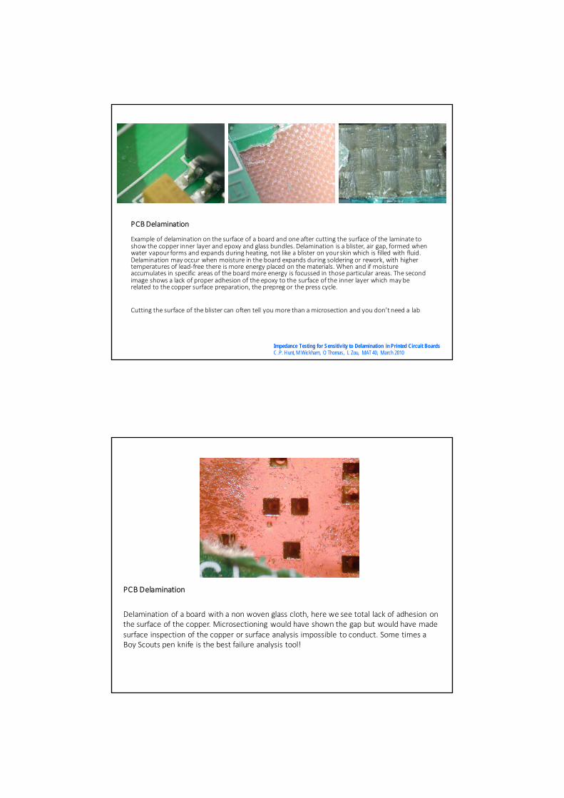
PCB Delamination
Example of delamination on the surface of a board and one after cutting the surface of the laminate to show the copper inner layer and epoxy and glass bundles. Delamination is a blister, air gap, formed when water vapour forms and expands during heating, not like a blister on your skin which is filled with fluid. Delamination may occur when moisture in the board expands during soldering or rework, with higher temperatures of lead‐free there is more energy placed on the materials. When and if moisture accumulates in specific areas of the board more energy is focussed in those particular areas. The second image shows a lack of proper adhesion of the epoxy to the surface of the inner layer which may be related to the copper surface preparation, the prepreg or the press cycle.
Cutting the surface of the blister can often tell you more than a microsection and you don’t need a lab
Impedance Testing for Sensitivity to Delamination in Printed Circuit BoardsC.P. Hunt, M Wickham, O Thomas, L Zou, MAT 40, March 2010
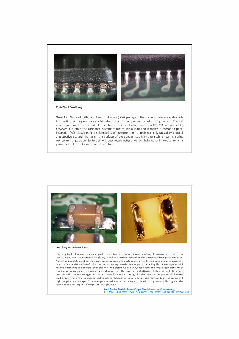
PCB Delamination
Delamination of a board with a non woven glass cloth, here we see total lack of adhesion on the surface of the copper. Microsectioning would have shown the gap but would have made surface inspection of the copper or surface analysis impossible to conduct. Some times a Boy Scouts pen knife is the best failure analysis tool!

Non Paste Coalescence
0201 chip component with lead‐free solder paste that has not fully reflowed in air. This is a common fault on small paste deposits whenpeople return to a traditional soak profile. Some solder pastes are farmore tolerant that others, the resulting solder joint is sound but theballs have not fully reflowed into the bulk of the solder joint.
This type of issue has been seen during 2003, 2004 on 0201 chip terminations and on 01005 chips in convection reflow but never invapour phase soldering due to the inert atmosphere during the soldering stages of the process. Basically the small solder paste deposit isexposed to a long period at elevated temperature during a lead‐free profile which reduces the performance of the flux in the paste. It isseen more with profiles that have a long pre‐heat like a traditional profile. A profile which does not have long dwell prior to reflow is lessaffected. Many paste suppliers have recommended the straight ramp profile but in the real world many users have not been able toachieve this with lead‐free on existing ovens. In most cases the actual joint is satisfactory and only the outer surface shows this effect;however, most people would not accept this type of process defect
Full copy of the Lead Free Experience Report http://www.bobwillis.co.uk/experience2006.pdf
Solder skip
Here is a solder skip mainly due to incorrect wave height as there is no evidence of solder on the pad or the termination. This may be a lead‐free joint but the principle behind the defect is the same. If there had been solder on the termination the process parameters may have been correct, problems with the pad solderability may have existed.
In the past skips have also been seen with different component suppliers and different lead forms on this type of capacitor. This type of component has the highest standoff for any components. When investigating skips look at the design, differences in component lead form and process issues like flux gassing and wave height.
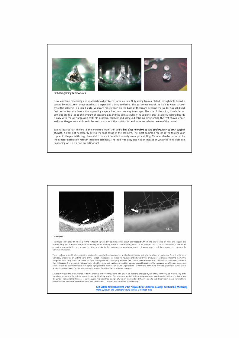
QFN/LGAWetting
Quad Flat No Lead (QFN) and Land Grid Array (LGA) packages often do not have solderable sideterminations or they are poorly solderable due to the component manufacturing process. There isnow requirement for the side terminations to be solderable based on IPC 610 requirements,however it is often the case that customers like to see a joint and it makes Automatic OpticalInspection (AOI) possible. Poor solderability of the edge termination is normally caused by a lack ofa protective coating like tin on the surface of the copper lead frame or resin smearing duringcomponent singulation. Solderability is best tested using a wetting balance or in production withpaste and a glass slide for reflow simulation
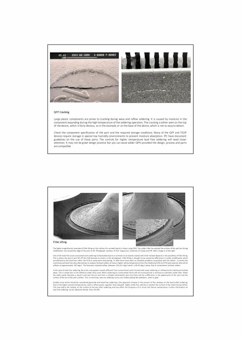
Leaching of terminations
If we step back a few years when companies first introduced surface mount, leaching of component terminationswas an issue. This was overcome by plating nickel as a barrier layer on to the silver/palladium paste end caps.Nickel has a much lower dissolution rate during soldering so leaching was virtually eliminated as a problem in theindustry. One additional benefit that the barrier plating provides is a longer solderability life. Some suppliers didnot implement the use of nickel over plating or the plating was so thin, these companies have seen problems oftermination loss at elevated temperatures. More recently this problem has led to joint failures in the field for oneuser. We will have to look again at the thickness of the nickel plating, plus the other barrier plating thicknessesused on zinc, iron and even copper lead frames to reduce intermetallic thicknesses forming during soldering andhigh temperature storage. Both examples lacked the barrier layer and failed during wave soldering and thesecond during testing for reflow process compatibility
Good Practice Guide to Reduce Copper Dissolution in Lead-Free Assembly,D. Di Maio, C. P. Hunt and B. Willis, Measurement Good Practice Guide No. 110, December 2008
PCB Outgassing & Blowholes
New lead‐free processing and materials: old problem, same causes. Outgassing from a plated through hole board iscaused by moisture in the printed board expanding during soldering. The gas comes out of the hole as water vapourwhile the solder is in a liquid state. Voids are mostly seen on the base of the board because the solder has solidifiedfirst on the top side hence the expanding vapour has only one way to escape. The size of the voids, blowholes orpinholes are related to the amount of escaping gas and the point at which the solder starts to solidify. Testing boardsis easy with the oil outgassing test: old problem, old test and same old solution. Conducting the test shows whereand how the gas escapes from holes and can show if the position is random or on selected areasof the barrel.
Baking boards can eliminate the moisture from the board but does wonders to the solderability of new surfacefinishes, it does not necessarily get to the root cause of the problem. The most common reason is the thickness ofcopper in the plated through hole which may not be able to evenly cover poor drilling. This can also be impacted bythe greater dissolution rates in lead‐free assembly. The lead‐free alloy also has an impact on what the joint looks likedepending on if it ’s a non eutectic or not
T in Whiskers
The images above show tin whiskers on the surface of a plated through hole printed circuit board coated with tin. The boards were produced and shipped to a
manufacturing site in Europe and when examined prior to assembly found to have whisker growth. Tin has become popula r on printed boards as one of the
alternative coating , tin has also become the finish of choice in the component manufacturing industry. However many people have shown concerns over the
formation of whiskers.
There has been a considerable amount of work and technical articles produced on whisker formation and potential for failure in electronics . There is still a lot of
work being undertaken around the world on this subject. The reason is we still do not have guaranteed whisker free products or the process where the chemis try is
being used is not being maintained correctly. If you follow guidelines on designing a whisker free process, use materials that should not form tin whiskers, somehow
they stil l appear. This problem is not specifically a lead‐free issue as it has been around for years as a possible problem. The increasing use of tin as a component
finish and printed boa rd alternative coating has highlighted the potential for failure. Organisations like NEMI and JEDEC have provided guidelines on what causes
whisker formation, ways of accelerating testing for whisker formation and preventative strategies
Current understanding is tin whiskers form due to stress formed in the plating. This causes tin filaments or single crystals of tin, commonly 2‐5 microns long to be
forced out from the surface of the plating during the life of the product. To reduce the possibility of formation engineers have looked at baking to reduce stress,
changing or increasing the thickness of barrier layers. This is the third example of whiskers examined on different products, each theoretically should have not have
occurred based on current recommendations and specifications. The other two are related to RF shielding
Test Method for Measurement of the Propensity for Conformal Coatings to Inhibit Tin WhiskeringMartin Wickham and Christopher Hunt, MAT28, December 2008
QFP Cracking
Large plastic components are prone to cracking during wave and reflow soldering. It is caused by moisture in thecomponent expanding during the high temperature of the soldering operation. The cracking is either seen on the topof the device, which is fairly obvious, as in the example,or on the base of the device, which is not so easy to detect.
Check the component specification of the part and the required storage conditions. Many of the QFP and TSOPdevices require storage in special low humidity environments to prevent moisture absorption. IPC have documentguidelines on the use of these parts. The controls for higher temperature lead free soldering will need closerattention. It may not be great design practice but you can wave solder QFPs provided the design, process and partsare compatible
Fillet Lifting
The highermagnification example of fil let lifting on the surface of a printed board is shown using SEM. The solder f illet has wetted the surface of the pad but duringsolidification has caused the edge of the joint to lift. Photograph courtesy of Prof. Suganuma, University of Osaka and ITRI. Bob’s image is on the right
One of the lead free issues associated with soldering tin/lead plated pa rts or printed circuit boards coated with thick tin/lead deposits is the possibil ity of fi llet lifting.This is where the pad or joint lift off the PCB laminate as shown in the photograph. Fillet lif ting is thought to be caused by differences in solder solidification whichare affected by the lead from either the PCB or component lead plating. To date there have been no reliability problems associated with this defect. Currently themost favoured lead free alloy alternatives to replace tin/lead solders all have a higher reflow temperature than the traditional 63% tin/37% lead eutectic alloywhichreflows at approximately 187 deg C. The favoured materials reflow between 210‐221 deg Cwhich is 30‐40 deg C above that of conventional tin/lead solders.
In the case of lead‐free soldering the joints may appear visually different from conventional joints formed with wave soldering or reflowedwith traditional tin/leadalloys. This is s imply due to the different solder alloy used. When soldering to a termination there will not necessarily be a continuous unbroken solder fille t. Whenthe solder paste becomes a liquid it wil l wet the pin and form a reliable intermetallic joint but there will be a difference in the appea rance of the joint and thesurface of the pin at the joint junction. This is commonly seen on soldering to any non fusible plating like palladium, silver or gold.
Another issue which should be considered generally with lead‐free soldering is the appa rent increase in the amount of flux residues on the boa rd after soldering.Due to the higher process temperatures used in reflow paste, suppliers have adopted higher solids flux vehicles to protect the surface of the metal during reflow.This may add to the residue on the surface of the pins after soldering and may affect the frequency of in circuit test fixture maintenance. Further information onlead free soldering can be obtained directly from the NPL.
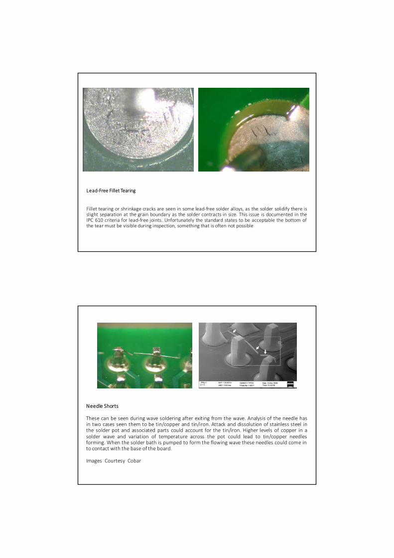
Lead‐Free Fillet Tearing
Fillet tearing or shrinkage cracks are seen in some lead‐free solder alloys, as the solder solidify there isslight separation at the grain boundary as the solder contracts in size. This issue is documented in theIPC 610 criteria for lead‐free joints. Unfortunately the standard states to be acceptable the bottom ofthe tear must be visible during inspection, something that is often not possible
Needle Shorts
These can be seen during wave soldering after exiting from the wave. Analysis of the needle hasin two cases seen them to be tin/copper and tin/iron. Attack and dissolution of stainless steel inthe solder pot and associated parts could account for the tin/iron. Higher levels of copper in asolder wave and variation of temperature across the pot could lead to tin/copper needlesforming. When the solder bath is pumped to form the flowing wave these needles could come into contact with the base of the board.
Images Courtesy Cobar
Poor Component Solderability
Example of poor solderability of SOT 23 terminations with lead‐free solder. This is a simple test forsolderability using a glass slide, the paste, stencil and reflow process used in production. It illustrates ifa process is contributing to soldering defects or just the components poor solderability. Clearly withthe components floating on the solder it is the parts that are the problem. A test procedure on simpletesting for solderability is available in IPC specification and as a poster set. The second image shows aprocess failure, the sample was aged and the result in production was a mirror of the test results inthis NPL solderability project
PPM Yields from LEADOUT Project

Electronics Academy Webinar Series
Counterfeit Component Inspection & DetectionWednesday 29th June 2016
Conformal Coating Inspection & Coating FaultsThursday 21st July 2016
Future webinars may cover
Bare PCB inspectionSolder paste and stencil inspectionCrimp connector and wire inspectionComponent inspection and recognitionMicrosection inspectionInspection of conductive adhesive jointsInspection of underfill and staked componentsDestructive solder joint assessment and inspection
Register on line at http://www.visioneng.com/electronics‐academy‐webinar‐series
Engineers Questions
If you have a process issue you would like us to consider in the webinar let us know?
Dewetting vs non‐wetting
We make SMT fasteners. We often have customer issues with poor solderability. We'd like to know how to ensure good solderability
Bad centring from MELF‐Diodes after reflow, with the result of short circuits to other components
How to effectively solder an MMA8452 16 pin QFN Package accelerometer onto a PCB. We are having lots of problems with this
What's the best way to remove solder balls underneath of parts?
QFNs and bottom terminated devices in general
Solder fill in termination cups
PCB and its components solder joints best practices, process, and validation for robust continuity and adhesion strength
Solder joint defects after reliability tests e.g . TC‐test. How to prevent
Proper QFN inspection with AOI
Problems with cold soldering on SMD parts QFN package
Cold soldering places, PCB surface with tin waves
Solder joint that looks good externally but causes test failure