Embed Size (px)
Citation preview

Solid State Device Fundamentals
ENS 345
Lecture Course
by
Alexander M. Zaitsev
Tel: 718 982 2812
Office 4N101b
College of Staten Island / CUNY Department of Engineering Science and Physics1
2. Crystals

College of Staten Island / CUNY Department of Engineering Science and Physics
Solid State Device Fundamentals
Solids
Crystal is a periodic atomic structure. This structure can be reproduced by translation of an elementary element which is known as unit cell. The least translation along one axis is known as lattice parameter.
2
Three types of solids, classified according to atomic arrangement
Crystalline Polyscrystalline Amorphous
2. Crystals

Department of Engineering Science and Physics
Solid State Device Fundamentals
Crystal lattice
The unit cell of a simple cubic lattice (a) along
with an image of 4 repeats in each direction (b).
Example of a complex
cubic lattice: Si crystal
lattice.
3College of Staten Island / CUNY
Different unit cells of cubic lattice:
primitive, body-centered, face-centered.
There are 7 types of crystal lattices (called Bravais lattices), shown below:
2. Crystals

College of Staten Island / CUNY Department of Engineering Science and Physics
Solid State Device Fundamentals
Crystallographic positions
Silicon crystal has so-called diamond type lattice. Each Si atom has 4 nearest neighbors
4
Crystallographic position is denoted by three numbers, which are coefficients of the position vector, e.g. ½ ½ ½ for the red atom in the example above.
2. Crystals

5College of Staten Island / CUNY Department of Engineering Science and Physics
Solid State Device Fundamentals
Crystallographic positions in Si crystal
5
What are the positions of the blue atoms in silicon unit cell?
Tetrahedron
2. Crystals

6College of Staten Island / CUNY Department of Engineering Science and Physics
Solid State Device Fundamentals
Crystallographic directions
6
Crystallographic direction is a direction between any two atoms of crystal lattice
[221]
Cubic lattice
Hexagonal lattice
2. Crystals

77College of Staten Island / CUNY Department of Engineering Science and Physics
Solid State Device Fundamentals
Crystallographic directions in Si crystal
7
What are the directions from red atom towards blue atoms in silicon unit cell?
2. Crystals

8College of Staten Island / CUNY Department of Engineering Science and Physics
Solid State Device Fundamentals
Crystallographic planes
Crystallographic planes are denoted by Miller indices.
3 5 3
1/3 1/5 1/3
5 3 5
(535)
2. Crystals

9College of Staten Island / CUNY Department of Engineering Science and Physics
Solid State Device Fundamentals
Crystallographic planes in Si crystal
What are the crystallographic planes comprising red atom and one of the blue atoms in silicon unit cell?
2. Crystals

10College of Staten Island / CUNY Department of Engineering Science and Physics
Solid State Device Fundamentals
Linear atomic density of crystallographic directions
Linear Atomic Density (LAD) of a crystallographic direction is measured by number of atoms per unit length along this direction.
The higher direction indices the lower linear density.
aLAD [100] = (0.5+0.5)/a
LAD [110] = (0.5+0.5)/ 2a
LAD [111] = (0.5+1+0.5)/ 3a
2. Crystals

11College of Staten Island / CUNY Department of Engineering Science and Physics
Solid State Device Fundamentals
Calculate LAD in silicon along [100], [110] and [111] directions.
LAD of crystallographic directions in Si crystal
2. Crystals

12College of Staten Island / CUNY Department of Engineering Science and Physics
Solid State Device Fundamentals
Atomic density of crystallographic planes
Atomic Density (AD) of crystallographic planes is measured by number of atoms per unit area.
The higher Miller indices the lower atomic density.
2. Crystals

13College of Staten Island / CUNY Department of Engineering Science and Physics
Solid State Device Fundamentals
Calculate AD in silicon for planes (100), (110)and (111) directions.
AD of crystallographic planes in Si crystal
2. Crystals
College of Staten Island / CUNY Department of Engineering Science and Physics
Solid State Device Fundamentals
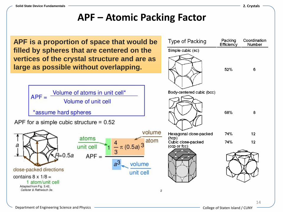
APF – Atomic Packing Factor
14
APF is a proportion of space that would be
filled by spheres that are centered on the
vertices of the crystal structure and are as
large as possible without overlapping.
2. Crystals

15College of Staten Island / CUNY Department of Engineering Science and Physics
Solid State Device Fundamentals
Show that APF of silicon is
APF of Si crystal lattice
2. Crystals

College of Staten Island / CUNY Department of Engineering Science and Physics
Solid State Device Fundamentals
Defects in crystals
29
0D defects (point defects)
1D defects (linear defects)
2D defects (planar defects)
3D defects(bulk defects)
2. Crystals